design and implementation of low-power digital signal ... · design and implementation of low-power...
TRANSCRIPT
www.ijsret.org
102 International Journal of Scientific Research Engineering & Technology (IJSRET), ISSN 2278 – 0882
Volume 4, Issue 2, February 2015
Design and Implementation of Low-Power Digital Signal
Processing using Approximate Adders
Shital Keskar, Prof T. S. Mote ENTC Department, Pune University, Pune, India
ABSTRACT Low power is an imperative requirement for portable
multimedia devices employing various signal processing
algorithms and architectures. In most multimedia
applications, human beings can gather useful
information from slightly erroneous outputs. Therefore,
we do not need to produce exactly correct numerical
outputs. Previous research in this context exploits error
resiliency primarily through voltage overscaling,
utilizing algorithmic and architectural techniques to
mitigate the resulting errors. In this paper, we propose
logic complexity reduction at the transistor level as an
alternative approach to take advantage of the relaxation
of numerical accuracy. We demonstrate this concept by
proposing various imprecise or approximate full adder
cells with reduced complexity at the transistor level, and
utilize them to design approximate multi-bit adders. In
addition to the inherent reduction in switched
capacitance, our techniques result in significantly shorter
critical paths, enabling voltage scaling.
Keyword—Approximate computing, low power, mirror
adder.
I. INTRODUCTION
Digital signal processing (DSP) blocks form the
backbone of various multimedia applications used in
portable devices. Most of these DSP blocks implement
image and video processing algorithms, where the
ultimate output is either an image or a video for human
consumption. Human beings have limited perceptual
abilities when interpreting an image or a video. This
allows the outputs of these algorithms to be numerically
approximate rather than accurate. This relaxation on
numerical exactness provides some freedom to carry out
imprecise or approximate computation. We can use this
freedom to come up with low-power designs at different
levels of design abstraction, namely, logic, architecture,
and algorithm.
The paradigm of approximate computing is specific to
select hardware implementations of DSP blocks. It is
shown in [1] that an embedded reduced instruction set
computing processor consumes 70% of the energy in
supplying data and instructions, and 6% of the energy
while performing arithmetic only. Therefore, using
approximate arithmetic in such a scenario will not
provide much energy benefit when considering the
complete processor. Programmable processors are
designed for general-purpose applications with no
application-specific specialization. Therefore, there may
not be many applications that will be able to tolerate
errors due to approximate computing. This also makes
general-purpose processors not suited for using
approximate building blocks. This issue has already been
discussed in [13]. Therefore, in this paper, we consider
application-specific integrated circuit implementations
of error-resilient applications like image and video
compression. We target the most computationally
intensive blocks in these applications and build them
using approximate hardware to show substantial
improvements in power consumption with little loss in
output quality.
Few works that focus on low-power design through
approximate computing at the algorithm and architecture
levels include algorithmic noise tolerance (ANT) [3]–
[6], significance driven computation (SDC) [7]–[9], and
nonuniform voltage overscaling (VOS) [10]. All these
techniques are based on the central concept of VOS,
coupled with additional circuitry for correcting or
limiting the resulting errors. In [11], a fast but
“inaccurate” adder is proposed. It is based on the idea
that on average, the length of the longest sequence of
propagate signals is approximately log n, where n is the
bitwidth of the two integers to be added. An error-
tolerant adder is proposed in [12] that operates by
splitting the input operands into accurate and inaccurate
parts. However, neither of these techniques target logic
complexity reduction. Power-efficient multiplier
architecture is proposed in [13] that uses a 2 × 2
inaccurate multiplier block resulting from Karnaugh map
simplification. This paper considers logic complexity
reduction using Karnaugh maps. Shin and Gupta [14]
and Phillips et al. [15] also proposed logic complexity
reduction by Karnaugh map simplification. Other works
that focus on logic complexity reduction at the gate level
are [16]–[19]. Other approaches use complexity
www.ijsret.org
103 International Journal of Scientific Research Engineering & Technology (IJSRET), ISSN 2278 – 0882
Volume 4, Issue 2, February 2015
reduction at the algorithm level to meet real-time energy
constraints [20], [21].
Previous works on logic complexity reduction have
focused on algorithm, logic, and gate levels. We propose
logic complexity reduction at the transistor level. We
apply this to addition at the bit level by simplifying the
mirror adder (MA) circuit. We develop imprecise but
simplified arithmetic units, which provide an extra layer
of power savings over conventional low-power design
techniques. This is attributed to the reduced logic
complexity of the proposed approximate arithmetic
units. Note that the approximate arithmetic units not
only have a reduced number of transistors, but care is
taken to ensure that the internal node capacitances are
greatly reduced. Complexity reduction leads to power
reduction in two different ways. First, an inherent
reduction in switched capacitance and leakage results
from having smaller hardware. Second, complexity
reduction frequently leads to shorter critical paths,
facilitating voltage reduction without any timing-
induced errors. In summary, our work significantly
differs from other works (SDC, ANT, and nonuniform
VOS) since we adopt a different approach for exploiting
error resiliency. Our aim is to target low-power design
using simplified and approximate logic implementations.
Since DSP blocks mainly consist of adders and
multipliers (which are, in turn, built using adders), we
propose several approximate adders, which can be used
effectively in such blocks.
A preliminary version of our work appeared in [22]. We
extend our paper in [22] by providing two more
simplified versions of the MA. Furthermore, we propose
a measure of the “quality” of a DSP block that uses
approximate adders. We also propose a methodology
that can be used to harness maximum power savings
using approximate adders, subject to a specific quality
constraint. Our contributions in this paper can be
summarized as follows.
1) We propose logic complexity reduction at the
transistor level as an alternative approach to approximate
computing for DSP applications.
2) We show how to simplify the logic complexity of a
conventional MA cell by reducing the number of
transistors and internal node capacitances. Keeping this
aim in mind, we propose five different simplified
versions of the MA, ensuring minimal errors in the full
adder (FA) truth table.
3) We utilize the simplified versions of the FA cell to
propose several imprecise or approximate multi-bit
adders that can be used as building blocks of DSP
systems. To maintain a reasonable output quality,
approximate FA cells used only in the least significant
bits (LSBs). We particularly focus on adder structures
that use FA cells as their basic building blocks.
4) VOS is a very popular technique to get large
improvements in power consumption. However, VOS
will lead to delay failures in the most significant bits
(MSBs). This might lead to large errors in corresponding
outputs and severely mess up the output quality of the
application. We use approximate FA cells only in the
LSBs, while the MSBs use accurate FA cells. Therefore,
at isofrequency, the errors introduced by VOS will be
much higher, when compared to proposed approximate
adders. Since truncation is a well-known technique to
facilitate voltage scaling,. In general, our approach may
be applied to any arithmetic circuit built with FAs.
II. APPROXIMATE ADDERS In this section, we discuss different methodologies for
designing approximate adders. Since the MA [23] is one
of the widely used economical implementations of an
FA [24], we use it as our basis for proposing different
approximations of an FA cell.
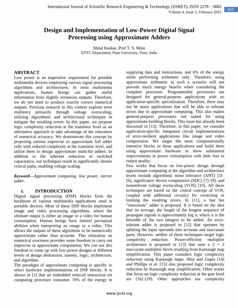
Fig. 1. Conventional MA.
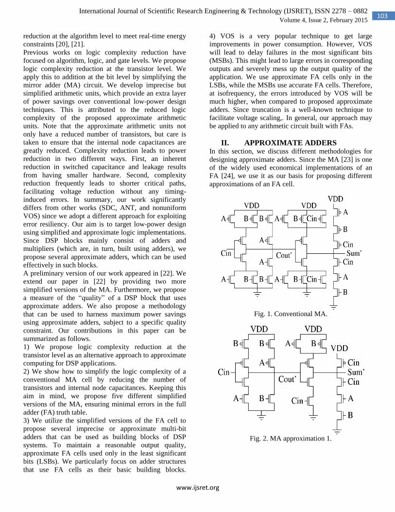
Fig. 2. MA approximation 1.
www.ijsret.org
104 International Journal of Scientific Research Engineering & Technology (IJSRET), ISSN 2278 – 0882
Volume 4, Issue 2, February 2015
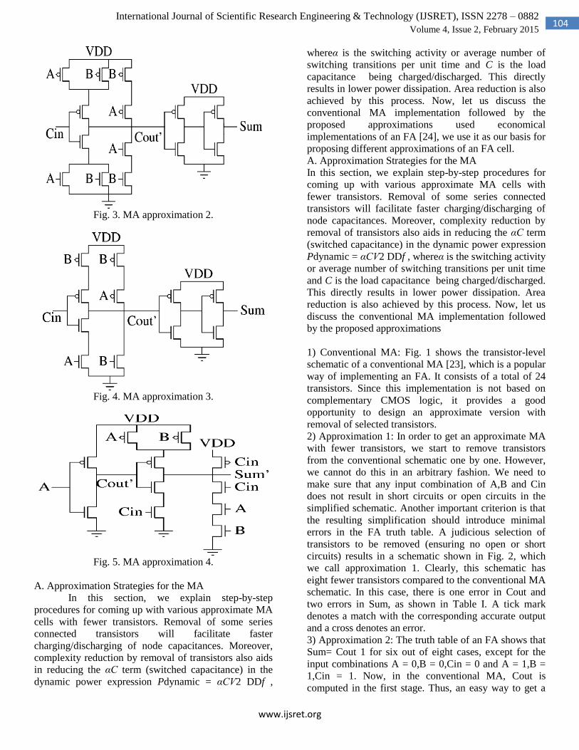
Fig. 3. MA approximation 2.
Fig. 4. MA approximation 3.
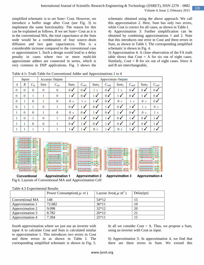
Fig. 5. MA approximation 4.
A. Approximation Strategies for the MA
In this section, we explain step-by-step
procedures for coming up with various approximate MA
cells with fewer transistors. Removal of some series
connected transistors will facilitate faster
charging/discharging of node capacitances. Moreover,
complexity reduction by removal of transistors also aids
in reducing the αC term (switched capacitance) in the
dynamic power expression Pdynamic = αCV2 DDf ,
whereα is the switching activity or average number of
switching transitions per unit time and C is the load
capacitance being charged/discharged. This directly
results in lower power dissipation. Area reduction is also
achieved by this process. Now, let us discuss the
conventional MA implementation followed by the
proposed approximations used economical
implementations of an FA [24], we use it as our basis for
proposing different approximations of an FA cell.
A. Approximation Strategies for the MA
In this section, we explain step-by-step procedures for
coming up with various approximate MA cells with
fewer transistors. Removal of some series connected
transistors will facilitate faster charging/discharging of
node capacitances. Moreover, complexity reduction by
removal of transistors also aids in reducing the αC term
(switched capacitance) in the dynamic power expression
Pdynamic = αCV2 DDf , whereα is the switching activity
or average number of switching transitions per unit time
and C is the load capacitance being charged/discharged.
This directly results in lower power dissipation. Area
reduction is also achieved by this process. Now, let us
discuss the conventional MA implementation followed
by the proposed approximations
1) Conventional MA: Fig. 1 shows the transistor-level
schematic of a conventional MA [23], which is a popular
way of implementing an FA. It consists of a total of 24
transistors. Since this implementation is not based on
complementary CMOS logic, it provides a good
opportunity to design an approximate version with
removal of selected transistors.
2) Approximation 1: In order to get an approximate MA
with fewer transistors, we start to remove transistors
from the conventional schematic one by one. However,
we cannot do this in an arbitrary fashion. We need to
make sure that any input combination of A,B and Cin
does not result in short circuits or open circuits in the
simplified schematic. Another important criterion is that
the resulting simplification should introduce minimal
errors in the FA truth table. A judicious selection of
transistors to be removed (ensuring no open or short
circuits) results in a schematic shown in Fig. 2, which
we call approximation 1. Clearly, this schematic has
eight fewer transistors compared to the conventional MA
schematic. In this case, there is one error in Cout and
two errors in Sum, as shown in Table I. A tick mark
denotes a match with the corresponding accurate output
and a cross denotes an error.
3) Approximation 2: The truth table of an FA shows that
Sum= Cout 1 for six out of eight cases, except for the
input combinations A = 0,B = 0,Cin = 0 and A = 1,B =
1,Cin = 1. Now, in the conventional MA, Cout is
computed in the first stage. Thus, an easy way to get a
www.ijsret.org
105 International Journal of Scientific Research Engineering & Technology (IJSRET), ISSN 2278 – 0882
Volume 4, Issue 2, February 2015
simplified schematic is to set Sum= Cout. However, we
introduce a buffer stage after Cout (see Fig. 3) to
implement the same functionality. The reason for this
can be explained as follows. If we set Sum= Cout as it is
in the conventional MA, the total capacitance at the Sum
node would be a combination of four source–drain
diffusion and two gate capacitances. This is a
considerable increase compared to the conventional case
or approximation 1. Such a design would lead to a delay
penalty in cases where two or more multi-bit
approximate adders are connected in series, which is
very common in DSP applications. Fig. 3 shows the
schematic obtained using the above approach. We call
this approximation 2. Here, Sum has only two errors,
while Cout is correct for all cases, as shown in Table I.
4) Approximation 3: Further simplification can be
obtained by combining approximations 1 and 2. Note
that this introduces one error in Cout and three errors in
Sum, as shown in Table I. The corresponding simplified
schematic is shown in Fig. 4.
5) Approximation 4: A close observation of the FA truth
table shows that Cout = A for six out of eight cases.
Similarly, Cout = B for six out of eight cases. Since A
and B are interchangeable,
Table 4.1: Truth Table for Conventional Adder and Approximations 1 to 4
Fig 6. Layouts of Conventional MA and Approximation Cell
Table 4.3 Experimental Results
Power Consumption( ) Layout Area( m2 ) Delay(ps)
Conventional MA 148 54*12 15
Approximation 1 72.682 36*11 10
Approximation 2 9.098 32*12 20
Approximation 3 8.782 26*12 21
Approximation 4 7.394 25*11 15
fourth approximation where we just use an inverter with
input A to calculate Cout and Sum is calculated similar
to approximation 1. This introduces two errors in Cout
and three errors in as shown in Table I. The
corresponding simplified schematic is shown in Fig. 5.
In all we consider Cout = A. Thus, we propose a Sum,
using an inverter with Cout as input.
6) Approximation 5: In approximation 4, we find that
there are three errors in Sum. We extend this
www.ijsret.org
106 International Journal of Scientific Research Engineering & Technology (IJSRET), ISSN 2278 – 0882
Volume 4, Issue 2, February 2015
approximation by allowing one more error, i.e., four
errors in Sum. We use the approximation Cout = A, as in
approximation 4. If we want to make Sum independent
of Cin, we have two choices, Sum= A and Sum= B.
Thus, we have two alternatives for approximation 5,
namely, Sum= A, Cout = A and Sum= B, Cout = A,
which are shown in Table II. The table shows which
entries match with and differ from the corresponding
accurate outputs (shown by tick marks and crosses). If
we observe choice 1, we find that both Sum and Cout
match with accurate outputs in only two out of eight
cases. In choice 2, Sum and Cout match with accurate
outputs in four out of eight cases. Therefore, to minimize
errors both in Sum and Cout, we go for choice 2 as
approximation 5. Our main thrust here is to ensure that
for a particular input combination (A,B and Cin),
ensuring correctness in Sum also makes Cout correct.
Now consider the addition of two 20-b integers a[19 : 0]
and b[19 : 0] using an RCA. Suppose we use
approximate FAs for 7 LSBs. Then, Cin[7] = Cout[6].
Note that Cout[6] is approximate. Applying this
approximation to our present example, we find that carry
propagation from bit 0 to bit 6 is entirely eliminated. In
addition, the circuitry needed to calculate Cout[0] to
Cout[5] is also saved. To limit the output capacitance at
Sum and Cout nodes, we implement approximation 5:
Sum= B, Cout = A using buffers.
Layouts of conventional MA and different
approximations in IBM 90-nm technology are shown in
Fig. 6. Layout area the conventional MA and different
approximations are compared in Table III.
Approximation 5 uses only buffers. The layout area of a
single buffer is 6.77 μm2.
Table 4.2. Choosing Approximation 5
B. Voltage Scaling Using Approximate Adders
Let us discuss how the proposed approximations
also help in reducing the overall propagation delay in a
typical design involving several adder levels. The input
capacitance of Cin in a conventional MA consists of six
gate capacitances (see Fig. 1). In approximation 1, this
value is reduced to five gate capacitances.
Approximation 4 has three such gate capacitances,
which further reduces to only two gate capacitances in
approximations 2 and 3. This result in faster charging/
discharging of Cout nodes during carry propagation.
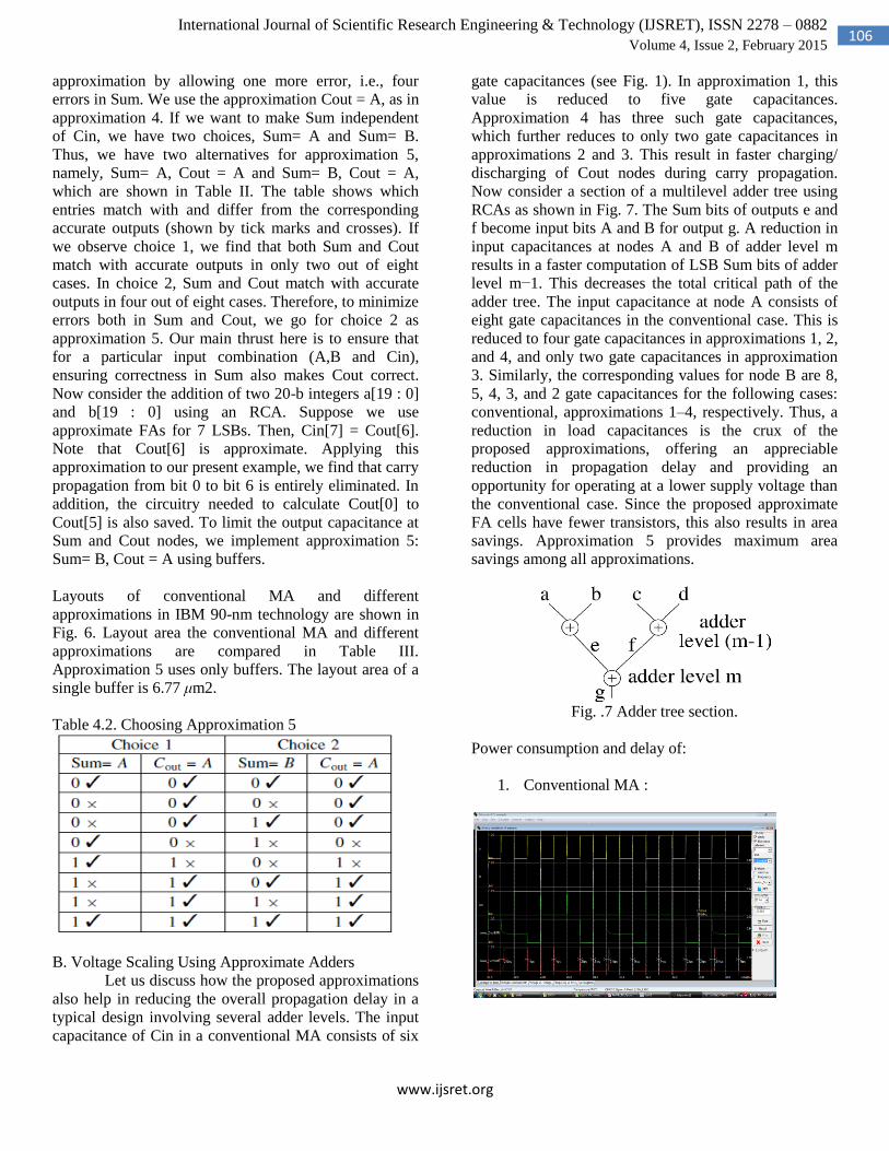
Now consider a section of a multilevel adder tree using
RCAs as shown in Fig. 7. The Sum bits of outputs e and
f become input bits A and B for output g. A reduction in
input capacitances at nodes A and B of adder level m
results in a faster computation of LSB Sum bits of adder
level m−1. This decreases the total critical path of the
adder tree. The input capacitance at node A consists of
eight gate capacitances in the conventional case. This is
reduced to four gate capacitances in approximations 1, 2,
and 4, and only two gate capacitances in approximation
3. Similarly, the corresponding values for node B are 8,
5, 4, 3, and 2 gate capacitances for the following cases:
conventional, approximations 1–4, respectively. Thus, a
reduction in load capacitances is the crux of the
proposed approximations, offering an appreciable
reduction in propagation delay and providing an
opportunity for operating at a lower supply voltage than
the conventional case. Since the proposed approximate
FA cells have fewer transistors, this also results in area
savings. Approximation 5 provides maximum area
savings among all approximations.
Fig. .7 Adder tree section.
Power consumption and delay of:
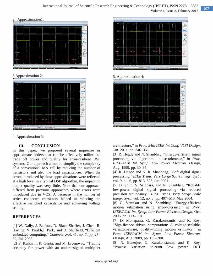
1. Conventional MA :
www.ijsret.org
107 International Journal of Scientific Research Engineering & Technology (IJSRET), ISSN 2278 – 0882
Volume 4, Issue 2, February 2015
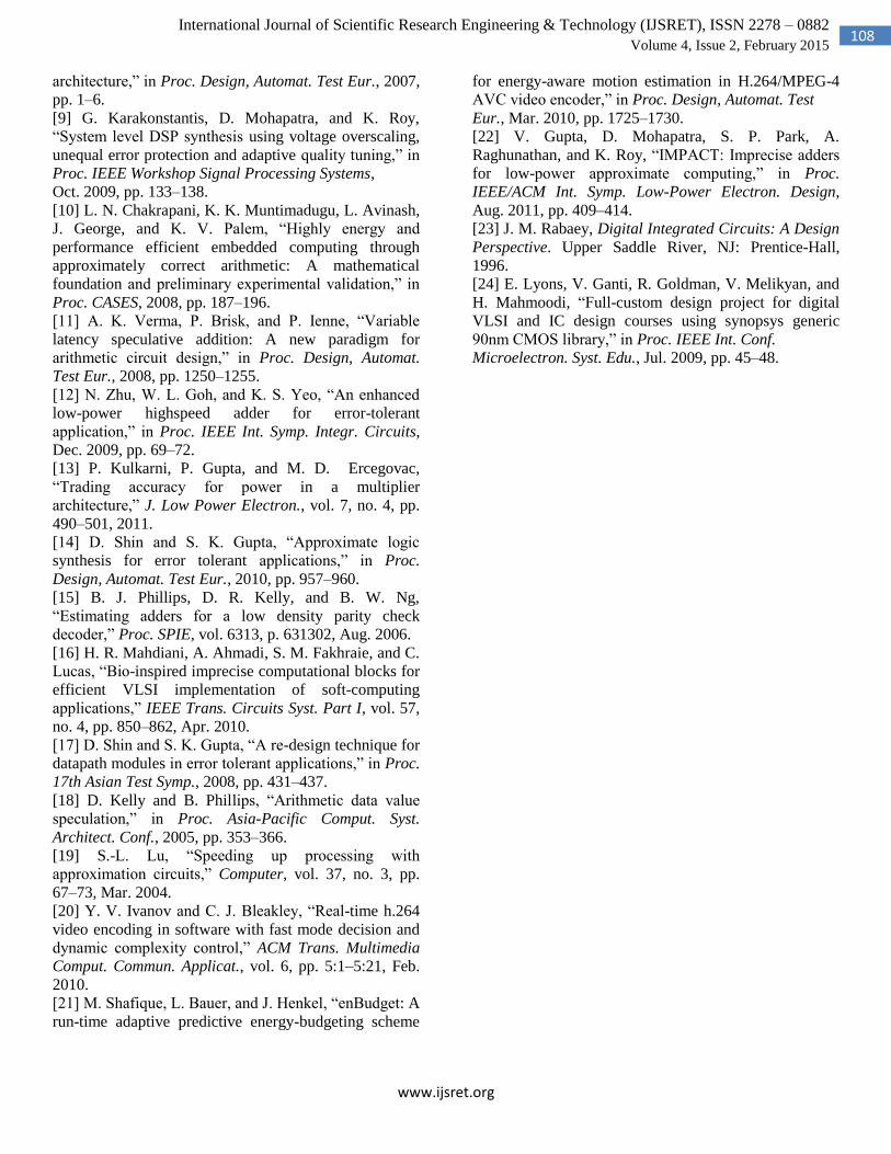
2. Approximation1:
3.Approximation 2:
4. Approximation 3:
5. Approximation 4:
III. CONCLUSION
In this paper, we proposed several imprecise or
approximate adders that can be effectively utilized to
trade off power and quality for error-resilient DSP
systems. Our approach aimed to simplify the complexity
of a conventional MA cell by reducing the number of
transistors and also the load capacitances. When the
errors introduced by these approximations were reflected
at a high level in a typical DSP algorithm, the impact on
output quality was very little. Note that our approach
differed from previous approaches where errors were
introduced due to VOS. A decrease in the number of
series connected transistors helped in reducing the
effective switched capacitance and achieving voltage
scaling.
REFERENCES
[1] W. Dally, J. Balfour, D. Black-Shaffer, J. Chen, R.
Harting, V. Parikh,J. Park, and D. Sheffield, “Efficient
embedded computing,” Computer,vol. 41, no. 7, pp. 27–
32, Jul. 2008.
[2] P. Kulkarni, P. Gupta, and M. Ercegovac, “Trading
accuracy for power with an underdesigned multiplier
architecture,” in Proc. 24th IEEE Int.Conf. VLSI Design,
Jan. 2011, pp. 346–351.
[3] R. Hegde and N. Shanbhag, “Energy-efficient signal
processing via algorithmic noise-tolerance,” in Proc.
IEEE/ACM Int. Symp. Low Power Electron. Design,
Aug. 1999, pp. 30–35.
[4] R. Hegde and N. R. Shanbhag, “Soft digital signal
processing,” IEEE Trans. Very Large Scale Integr. Syst.,
vol. 9, no. 6, pp. 813–823, Jun.2001.
[5] B. Shim, S. Sridhara, and N. Shanbhag, “Reliable
low-power digital signal processing via reduced
precision redundancy,” IEEE Trans. Very Large Scale
Integr. Syst., vol. 12, no. 5, pp. 497–510, May 2004.
[6] G. Varatkar and N. Shanbhag, “Energy-efficient
motion estimation using error-tolerance,” in Proc.
IEEE/ACM Int. Symp. Low Power Electron.Design, Oct.
2006, pp. 113–118.
[7] D. Mohapatra, G. Karakonstantis, and K. Roy,
“Significance driven computation: A voltage-scalable,
variation-aware, quality-tuning motion estimator,” in
Proc. IEEE/ACM Int. Symp. Low Power Electron.
Design, Aug. 2009, pp. 195–200.
[8] N. Banerjee, G. Karakonstantis, and K. Roy,
“Process variation tolerant low power DCT
www.ijsret.org
108 International Journal of Scientific Research Engineering & Technology (IJSRET), ISSN 2278 – 0882
Volume 4, Issue 2, February 2015
architecture,” in Proc. Design, Automat. Test Eur., 2007,
pp. 1–6.
[9] G. Karakonstantis, D. Mohapatra, and K. Roy,
“System level DSP synthesis using voltage overscaling,
unequal error protection and adaptive quality tuning,” in
Proc. IEEE Workshop Signal Processing Systems,
Oct. 2009, pp. 133–138.
[10] L. N. Chakrapani, K. K. Muntimadugu, L. Avinash,
J. George, and K. V. Palem, “Highly energy and
performance efficient embedded computing through
approximately correct arithmetic: A mathematical
foundation and preliminary experimental validation,” in
Proc. CASES, 2008, pp. 187–196.
[11] A. K. Verma, P. Brisk, and P. Ienne, “Variable
latency speculative addition: A new paradigm for
arithmetic circuit design,” in Proc. Design, Automat.
Test Eur., 2008, pp. 1250–1255.
[12] N. Zhu, W. L. Goh, and K. S. Yeo, “An enhanced
low-power highspeed adder for error-tolerant
application,” in Proc. IEEE Int. Symp. Integr. Circuits,
Dec. 2009, pp. 69–72.
[13] P. Kulkarni, P. Gupta, and M. D. Ercegovac,
“Trading accuracy for power in a multiplier
architecture,” J. Low Power Electron., vol. 7, no. 4, pp.
490–501, 2011.
[14] D. Shin and S. K. Gupta, “Approximate logic
synthesis for error tolerant applications,” in Proc.
Design, Automat. Test Eur., 2010, pp. 957–960.
[15] B. J. Phillips, D. R. Kelly, and B. W. Ng,
“Estimating adders for a low density parity check
decoder,” Proc. SPIE, vol. 6313, p. 631302, Aug. 2006.
[16] H. R. Mahdiani, A. Ahmadi, S. M. Fakhraie, and C.
Lucas, “Bio-inspired imprecise computational blocks for
efficient VLSI implementation of soft-computing
applications,” IEEE Trans. Circuits Syst. Part I, vol. 57,
no. 4, pp. 850–862, Apr. 2010.
[17] D. Shin and S. K. Gupta, “A re-design technique for
datapath modules in error tolerant applications,” in Proc.
17th Asian Test Symp., 2008, pp. 431–437.
[18] D. Kelly and B. Phillips, “Arithmetic data value
speculation,” in Proc. Asia-Pacific Comput. Syst.
Architect. Conf., 2005, pp. 353–366.
[19] S.-L. Lu, “Speeding up processing with
approximation circuits,” Computer, vol. 37, no. 3, pp.
67–73, Mar. 2004.
[20] Y. V. Ivanov and C. J. Bleakley, “Real-time h.264
video encoding in software with fast mode decision and
dynamic complexity control,” ACM Trans. Multimedia
Comput. Commun. Applicat., vol. 6, pp. 5:1–5:21, Feb.
2010.
[21] M. Shafique, L. Bauer, and J. Henkel, “enBudget: A
run-time adaptive predictive energy-budgeting scheme
for energy-aware motion estimation in H.264/MPEG-4
AVC video encoder,” in Proc. Design, Automat. Test
Eur., Mar. 2010, pp. 1725–1730.
[22] V. Gupta, D. Mohapatra, S. P. Park, A.
Raghunathan, and K. Roy, “IMPACT: Imprecise adders
for low-power approximate computing,” in Proc.
IEEE/ACM Int. Symp. Low-Power Electron. Design,
Aug. 2011, pp. 409–414.
[23] J. M. Rabaey, Digital Integrated Circuits: A Design
Perspective. Upper Saddle River, NJ: Prentice-Hall,
1996.
[24] E. Lyons, V. Ganti, R. Goldman, V. Melikyan, and
H. Mahmoodi, “Full-custom design project for digital
VLSI and IC design courses using synopsys generic
90nm CMOS library,” in Proc. IEEE Int. Conf.
Microelectron. Syst. Edu., Jul. 2009, pp. 45–48.