design and fabrication of nano-structured gradient index microlenses
TRANSCRIPT
Design and fabrication ofnano-structured gradient index
microlenses
F. Hudelist, R. Buczynski, A.J. Waddie, M.R. TaghizadehHeriot Watt University, School of Engineering and Physical Sciences,
Edinburgh, UK, EH14 4AS
Abstract: We present a novel fabrication technology for nano-structuredgraded index micro-optical components, based on the stack-and-drawmethod used for photonic crystal fibres. These discrete structures can bedescribed with an effective refractive index distribution. Furthermore wepresent spherical nano-structured microlenses with a flat facet fabricatedwith this method and designed using an algorithm based on the Maxwell-Garnett mixing formula. Finally we show theoretical verification by usingFDTD simulations for a nano-structured lens as well as experimental dataobtained in the microwave regime.
© 2009 Optical Society of America
OCIS codes: (220.3630) Lenses; (230.3990) Micro-optical devices; (260.2065) Effectivemedium theory
References and links1. C. Gomez-Reino, M. V. Perez, and C. Bao, Gradient-Index Optics - Fundamentals and Applications (Springer,
2002).2. L. Hao, S. Bangren, W. Jijiang, G. Lijun, and L. Aimei, “Fabrication of gradient refractive index ball lenses,”
Opt. Lasers Eng. 46, 252–256 (2007).3. M. Bass, Handbook of Optics, chap. 9 (McGraw-Hill Professional, 2000).4. A. Bjarklev, J. Broeng, and A. Bjarklev, Photonic Crystal Fibres (Kluwer Academic Publishers, 2003).5. H. Kurt, E. Colak, O. Cakmak, H. Caglayan, and E. Ozbay, “The focusing effect of graded index photonic
crystals,” Appl. Phys. Lett. 93, 171,108 (2008), http://link.aip.org/link/?APL/93/171108/1.6. A. Sihvola, Electromagnetic mixing formulas and applications (Institution of Electrical Engeneers, London, UK,
1999).7. L. Li, “New formulation of the Fourier modal method for crossed surface-relief gratings,” J. Opt. Soc. Am. A
14(10), 2758–2767 (1997).8. E. Popov and M. Neviere, “Maxwell equations in Fourier space: fast-converging formulation for diffraction by
arbitrary shaped, periodic, anisotropic media,” J. Opt. Soc. Am. A 18(11), 2886–2894 (2001).9. A. Taflove and S. Hagness, Computational Electrodynamics: The Finite-Difference Time-Domain Method
(Artech House, Norwood, MA, 2005).10. S. Kirkpatrick, C. Gelatt Jr, and M. Vecchi, “Optimization by Simulated Annealing,” Science 220, 671 (1983).11. E. Hecht, Optics, 4th ed. (Addison Wesley, 2002).12. D. Lorenc, M. Aranyosiova, R. Buczynski, R. Stepien, I. Bugar, A. Vincze, and D. Velic, “Nonlinear refractive
index of multicomponent glasses designed for fabrication of photonic crystal fibers,” Appl. Phys. B: Lasers Opt.pp. 531–538 (2008).
13. Z. Sacks, D. Kingsland, R. Lee, and J. Lee, “A Perfectly Matched anisotropic absorber for use as an absorbingboundary condition.” IEEE Trans. Antenn. Propag. 43, 1460–1463 (1995).
14. F. Luan, A. K. George, T. D. Hedley, G. J. Pearce, D. M. Bird, J. C. Knight, and P. S. J. Russell, “All-solidphotonic bandgap fiber,” Opt. Lett. 29, 2369–2371 (2004), http://ol.osa.org/abstract.cfm?URI=ol-29-20-2369.
15. X. Feng, T. Monro, P. Petropoulos, V. Finazzi, and D. Hewak, “Solid microstructured optical fiber,” Opt. Express11, 2225–2230 (2003), http://www.opticsexpress.org/abstract.cfm?URI=oe-11-18-2225.
#104698 - $15.00 USD Received 30 Nov 2008; revised 16 Jan 2009; accepted 6 Feb 2009; published 17 Feb 2009
(C) 2009 OSA 2 March 2009 / Vol. 17, No. 5 / OPTICS EXPRESS 3255
16. G. Bouwmans, L. Bigot, Y. Quiquempois, F. Lopez, L. Provino, and M. Douay, “Fabrication and characterizationof an all-solid 2D photonic bandgap fiber with a low-loss region (< 20 dB/km) around 1550 nm,” Opt. Express13(21), 8452–8459 (2005), http://www.opticsexpress.org/abstract.cfm?URI=oe-13-21-8452.
17. T. Huang, Z. Li, M. Li, D. Chetwynd, and C. Gosselin, “Conceptual design and dimensional synthesis of a novel2-DOF translational parallel robot for pick-and-place operations,” Journal of Mechanical Design 126, 449–455(2004).
18. J. Birch, G. Simonis, M. Afsar, R. Clarke, J. Dutta, H. Frost, X. Gerbaux, A. Hadni, W. Hall, R. Heidinger, W. Ho,C. Jones, F. Koniger, R. Moore, H. Matsuo, T. Nakano, W. Richter, K. Sakai, M. Stead, U. Stumper, R. Vigil,and T. Wells, “An intercomparison of measurement techniques for the determination of the dielectric propertiesof solids at near millimetre wavelengths,” IEEE T. Microw. Theory. 42, 956–965 (1994).
1. Introduction
Gradient index components are a class of micro optical elements which obtain their opticalfunctionality by changes of the refractive index without changing the surface profile. They aremost commonly used as gradient index (GRIN) lenses [1]. The typical approach to fabricateradial gradient index materials is based on ion exchange [2], or by forming the gradient byleaching or by stuffing in a sol-gel formed glass [3]. These technologies allow only monotonicrefractive index distributions with only very small contrasts.
Here we present a high volume fabrication technology for nano-structured dielectric elementswhich can be considered as gradient index materials with arbitrary index distributions withinthe limits of the refractive index constants of about Δn ≈ 0.3 and a maximum gradient of aboutΔn ≈ 0.3 per µm . They can be designed not only as microlenses but also as general arbitrarydiffractive and refractive elements.
The technology introduced in this paper is based on the fabrication method for photoniccrystal fibres (PCF), in particular all solid PCFs [4]. The optical functionality is achieved byassembling two materials in a binary subwavelength pattern which shows the behavior of acontinuous gradient index material. The obtained micro-optical components have a flat facetand a profile of the refractive index dependent on the material distribution. Possible applica-tions include microlenses and microlens arrays as well as general phase correctors. The featuresizes of the elements can range down to 100nm and less. Unlike conventional diffusion basedmethods for fabricating gradient index materials our approach allows us to obtain arbitrary non-monotonic refractive index profiles and it is also possible to create microlens arrays with 100%fill factor in one fabrication procedure.
The focusing effect of gradient index photonic crystals has recently been reported for 2Dphotonic crystals [5]. In this approach the focusing is related to the resonance between adjacentholes with varying distance between the holes. The approach taken in this paper differs from thisdescription: here we treat the pattern of a binary structure with very small features comparedto the wavelength as an effective medium. The focusing effect can then be explained by aneffective gradient index profile.
Dielectric structures with an unclustered distribution of the refractive index and feature sizessmall compared to the wavelength of the incident light can be treated as a continuous gradientindex material by applying the Maxwell-Garnett mixing formula.
2. Design of nano-structured gradient index micro-optical components
In this section we introduce a new description of arbitrary two dimensional dielectric structureswith out of plane illumination. We are considering non absorbing discrete dielectric structuresassembled from materials with different refractive indices and feature sizes that are small com-pared to the wavelength. Locally, on the wavelength scale, the materials are statistically dis-tributed which results in an effective refractive index that can be calculated by averaging therefractive index over a certain neighbourhood. On the whole structure the fill factor of each
#104698 - $15.00 USD Received 30 Nov 2008; revised 16 Jan 2009; accepted 6 Feb 2009; published 17 Feb 2009
(C) 2009 OSA 2 March 2009 / Vol. 17, No. 5 / OPTICS EXPRESS 3256
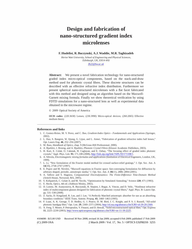
(a) (b) (c)
Fig. 1. Design of a nano-structures microlens: (a) the index pattern of the nano-structured lens;(b) the effective index distribution of (a) calculated with equation 1; (c) the ideal parabolic dis-tribution used for the reference lens.
material has a defined distribution to achieve the desired index profile. The analysis of thesestructures is based on the Maxwell Garnett mixing formula [6]. The optical properties of ma-terial compounds with small feature sizes compared to the wavelength can be treated as aneffective yield of the compound’s properties such as the fill factor of each material and theshape of the elements. In the case of a circular or hexagonal pixel shape the random mediummodel can be applied to calculate the effective permittivity:
εe f f =< ε > − f (ε1 − ε2)ε1− < ε >
3 < ε >(1)
where ε1 and ε2 are the permittivities of the two glasses, < ε >= ε2 + f (ε1−ε2) and f is the fillfactor of ε1. Due to the very similar permittivities of the glasses used in the presented fabrica-tion technology the difference between εe f f and < ε > is in the order of 10−4εe f f and thereforewe can assume εe f f =< ε > for our calculations. To obtain the effective permittivity distribu-tion from the pixelated binary pattern, the effective permittivity for each pixel is calculatedby averaging over a neighbourhood of about 1.5λ or less which results in a continuous indexdistribution that can be treated as a gradient index material.
A strict upper limit for the accuracy of this approximation cannot be made as it depends onseveral factors such as the pattern and the index contrast of the materials. We could howevershow this approximation to be accurate in most cases for pixel sizes of about λ/10 and smaller.The experimental results described in section 6 show focusing for an element with feature sizesof λ/5, however the focus is not diffraction limited. In this case a rigorous treatment such asthe Fourier modal method [7, 8] or the FDTD method [9] has to be applied to calculate the fieldpropagation accurately.
A good approach for the search of the required material distribution is simulated annealing[10], a Monte Carlo method similar to the direct binary search, with the advantage that localminima of the cost function are more likely to be avoided. The cost function gives an indicationof the quality of the pattern by calculating how well the current index distribution matchesthe target. We consider the standard deviation of the averaged index distribution to the desiredindex pattern as cost function:
c =1P
(P
∑p=1
(ne f f (p)−N(p))2
)1/2
(2)
#104698 - $15.00 USD Received 30 Nov 2008; revised 16 Jan 2009; accepted 6 Feb 2009; published 17 Feb 2009
(C) 2009 OSA 2 March 2009 / Vol. 17, No. 5 / OPTICS EXPRESS 3257
where ne f f (p) = ε2e f f is the effective index at point p, N(p) is the desired index value respec-
tively and P is the total number of rods of which the structure is assembled.The index profile of a radial GRIN lens is typically parabolic [11]:
n(r) = nmax(1−ar2/2) (3)
where nmax is the maximum refractive at the center of the lens, r is the diameter and a is aconstant. The pitch length of the GRIN lens is then given as p = 2πa−0.5.
The design process starts with a random material distribution for the pixels. In eachiteration step the material of one random pixel is changed and the new cost functioncNEW is calculated. The change is accepted if cNEW < cOLD and with a probability ofp = k · exp{−(cNEW − cOLD)/T (I)} if cNEW ≥ cOLD where k is a constant and T(I) is a pa-rameter that is decreased exponentially with the number of iteration steps.
Figure 1(a) shows the result for a design of a spherical microlens. The effective index dis-tribution calculated with equation 1 is very close to the desired parabolic index profile.
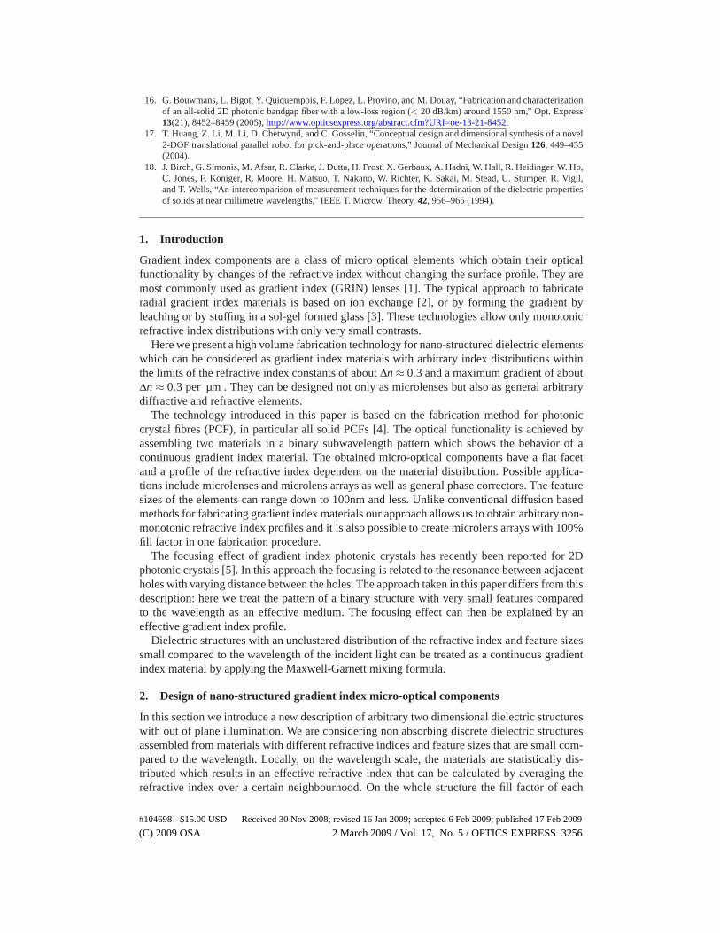
3. Verification of the Maxwell-Garnett approach using FDTD simulations
(a) The field distribution in the x-z-plane of the nano-structured lens for y=0
(b) Field distribution in the x-z-plane of an ideal gradient index lens with a parabolic refractiveindex distribution for y=0
Fig. 2. FDTD simulations comparing an ideal GRIN lens with the structured lens
To verify our concept of developing gradient index elements by mixing materials we performeda sequence of 3D FDTD simulations comparing the light propagation in an ideal gradient indexlens and in the nano-structured lens shown in Fig. 1(a). As refractive indices we used data fromthermally matched glasses that are used for the fabrication of such structures. The two glassesare NC21A, a borosilicate glass developed in house, and F2, a lead-silicate glass supplied bySCHOTT AG. For the exact optical properties refer to the paper by Lorenc et al [12]. The redareas in Fig. 1 represent F2 glass (nD = 1.60), the blue areas represent NC21A glass (nD = 1.51)respectively. The diameter of the lens is 10 µm with a feature size of 200 nm. The simulationswere performed with a plane wave illumination with λ = 1 µm , a spatial step size of 40nm,and a temporal step size of 6.67·10−17s. The computational space is terminated by the perfectlymatched layer boundary condition [13]. Figure 2(a) shows the light propagation inside the nano
#104698 - $15.00 USD Received 30 Nov 2008; revised 16 Jan 2009; accepted 6 Feb 2009; published 17 Feb 2009
(C) 2009 OSA 2 March 2009 / Vol. 17, No. 5 / OPTICS EXPRESS 3258
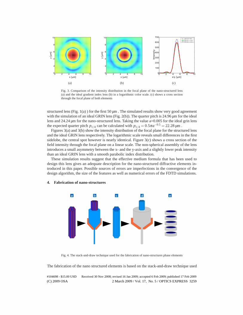
(a) (b) (c)
Fig. 3. Comparison of the intensity distribution in the focal plane of the nano-structured lens(a) and the ideal gradient index lens (b) in a logarithmic color scale. (c) shows a cross sectionthrough the focal plane of both elements
structured lens (Fig. 1(a) ) for the first 50 µm . The simulated results show very good agreementwith the simulation of an ideal GRIN lens (Fig. 2(b)). The quarter pitch is 24.96 µm for the ideallens and 24.24 µm for the nano-structured lens. Taking the value a=0.005 for the ideal grin lensthe expected quarter pitch p1/4 can be calculated with p1/4 = 0.5πa−0.5 = 22.28 µm .
Figures 3(a) and 3(b) show the intensity distribution of the focal plane for the structured lensand the ideal GRIN lens respectively. The logarithmic scale reveals small differences in the firstsidelobe, the central spot however is nearly identical. Figure 3(c) shows a cross section of thefield intensity through the focal plane on a linear scale. The non-spherical assembly of the lensintroduces a small asymmetry between the x- and the y-axis and a slightly lower peak intensitythan an ideal GRIN lens with a smooth parabolic index distribution.
These simulation results suggest that the effective medium formula that has been used todesign this lens gives an adequate description for the nano-structured diffractive elements in-troduced in this paper. Possible sources of errors are imperfections in the convergence of thedesign algorithm, the size of the features as well as numerical errors of the FDTD simulations.
4. Fabrication of nano-structures
Fig. 4. The stack-and-draw technique used for the fabrication of nano-structures phase elements
The fabrication of the nano structured elements is based on the stack-and-draw technique used
#104698 - $15.00 USD Received 30 Nov 2008; revised 16 Jan 2009; accepted 6 Feb 2009; published 17 Feb 2009
(C) 2009 OSA 2 March 2009 / Vol. 17, No. 5 / OPTICS EXPRESS 3259
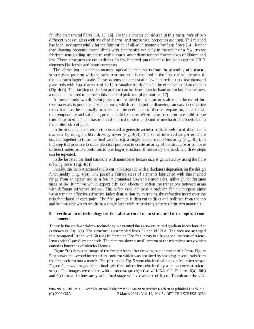
for photonic crystal fibres [14, 15, 16]. For the elements considered in this paper, rods of twodifferent types of glass with matched thermal and mechanical properties are used. This methodhas been used successfully for the fabrication of all-solid photonic bandgap fibres [14]. Ratherthan drawing photonic crystal fibres with feature size typically in the order of a few µm wefabricate non-guiding structures with a much larger diameter and feature sizes of 200nm andless. These structures are cut to discs of a few hundred µm thickness for use as optical GRINelements like lenses and beam correctors.
The fabrication of a nano structured optical element starts from the assembly of a macro-scopic glass preform with the same structure as it is required in the final optical element al-though much larger in scale. These patterns can consist of a few hundreds up to a few thousandglass rods with final diameter of λ/10 or smaller for designs in the effective medium domain(Fig. 4(a)). The stacking of the first preform can be done either by hand or, for larger structures,a robot can be used to perform this standard pick-and-place routine [17].
At present only two different glasses are included in the structures although the use of fur-ther materials is possible. The glass rods, which are of similar diameter, can vary in refractiveindex but must be thermally matched, i.e. the coefficient of thermal expansion, glass transi-tion temperature and softening point should be close. When these conditions are fulfilled thenano structured element has minimal internal tension and similar mechanical properties to amonolithic slab of glass.
In the next step, the preform is processed to generate an intermediate preform of about 2 mmdiameter by using the fibre drawing tower (Fig. 4(b)). The set of intermediate performs arestacked together to form the final pattern, e.g. a single lens or micro-lens array (Fig. 4(c)). Inthis step it is possible to stack identical preforms to create an array of the structure or combinedifferent intermediate preforms to one larger structure. If necessary the stack and draw stepscan be repeated.
In the last step the final structure with nanometer feature size is generated by using the fibredrawing tower (Fig. 4(d)).
Finally, the nano structured rod is cut into discs and with a thickness dependent on the designfunctionality (Fig. 4(e)). The possible feature sizes of elements fabricated with this methodrange from an upper end of a few micrometers down to nanometers, although for featuressizes below 10nm we would expect diffusion effects to soften the transitions between areaswith different refractive indices. This effect does not pose a problem for our purpose sincewe assume an effective refractive index distribution by averaging the refractive index over theneighbourhood of each point. The final product is then cut to disks and polished from the topand bottom side which results in a single layer with an arbitrary pattern of the two materials.
5. Verification of technology for the fabrication of nano-structured micro-optical com-ponents
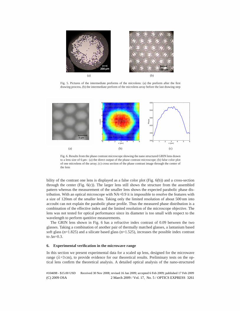
To verify the stack-and-draw technology we created the nano-structured gradient index lens thatis shown in Fig. 1(a). The structure is assembled from F2 and NC21A. The rods are arrangedin a hexagonal lattice with 50 rods in diameter. The final array is a hexagonal pattern of micro-lenses with 6 µm diameter each. The pictures show a small section of the microlens array whichcontains hundreds of identical lenses
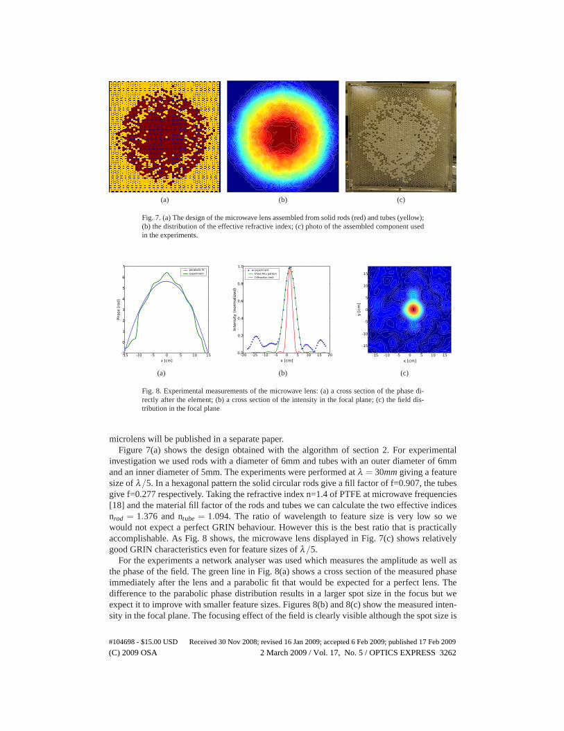
Figure 5(a) shows an image of the first preform after drawing to a diameter of 1.9mm. Figure5(b) shows the second intermediate preform which was obtained by stacking several rods fromthe first preform into a matrix. The pictures in Fig. 5 were obtained with an optical microscope.Figure 6 shows images of the final spherical micro-lens obtained by a phase contrast micro-scope. The images were taken with a microscope objective with NA=0.9. Pictures 6(a), 6(b)and 6(c) show the lens array at its final stage with a diameter of 6 µm . To enhance the visi-
#104698 - $15.00 USD Received 30 Nov 2008; revised 16 Jan 2009; accepted 6 Feb 2009; published 17 Feb 2009
(C) 2009 OSA 2 March 2009 / Vol. 17, No. 5 / OPTICS EXPRESS 3260
(a) (b)
Fig. 5. Pictures of the intermediate preforms of the microlens: (a) the preform after the firstdrawing process, (b) the intermediate preform of the microlens array before the last drawing step
(a) (b) (c)
Fig. 6. Results from the phase contrast microscope showing the nano structured GRIN lens drawnto a lens size of 6 µm : (a) the direct output of the phase contrast microscope; (b) false color plotof one microlens of the array; (c) cross section of the phase contrast image through the center ofthe lens
bility of the contrast one lens is displayed as a false color plot (Fig. 6(b)) and a cross-sectionthrough the center (Fig. 6(c)). The larger lens still shows the structure from the assembledpattern whereas the measurement of the smaller lens shows the expected parabolic phase dis-tribution. With an optical microscope with NA=0.9 it is impossible to resolve the features witha size of 120nm of the smaller lens. Taking only the limited resolution of about 500 nm intoaccoubt can not explain the parabolic phase profile. Thus the measured phase distribution is acombination of the effective index and the limited resolution of the microscope objective. Thelens was not tested for optical performance since its diameter is too small with respect to thewavelength to perform qantitive measurements.
The GRIN lens shown in Fig. 6 has a refractive index contrast of 0.09 between the twoglasses. Taking a combination of another pair of thermally matched glasses, a lantanium basedsoft glass (n=1.825) and a silicate based glass (n=1.525), increases the possible index contrastto Δn=0.3.
6. Experimental verification in the microwave range
In this section we present experimental data for a scaled up lens, designed for the microwaverange (λ=3 cm), to provide evidence for our theoretical results. Preliminary tests on the op-tical lens confirm the theoretical analysis. A detailed optical analysis of the nano-structured
#104698 - $15.00 USD Received 30 Nov 2008; revised 16 Jan 2009; accepted 6 Feb 2009; published 17 Feb 2009
(C) 2009 OSA 2 March 2009 / Vol. 17, No. 5 / OPTICS EXPRESS 3261
(a) (b) (c)
Fig. 7. (a) The design of the microwave lens assembled from solid rods (red) and tubes (yellow);(b) the distribution of the effective refractive index; (c) photo of the assembled component usedin the experiments.
-15 -10 -5 0 5 10 15
x [cm]
-1
0
1
2
3
4
5
6
7
Phase[rad]
parabolic fit
experiment
(a)
-20 -15 -10 -5 0 5 10 15 20
x [cm]
0.0
0.2
0.4
0.6
0.8
1.0
Intensity(norm
alized)
experiment
fitted Airy pattern
Diffraction limit
(b)
-15 -10 -5 0 5 10 15
x [cm]
-15
-10
-5
0
5
10
15
y[cm]
(c)
Fig. 8. Experimental measurements of the microwave lens: (a) a cross section of the phase di-rectly after the element; (b) a cross section of the intensity in the focal plane; (c) the field dis-tribution in the focal plane
microlens will be published in a separate paper.Figure 7(a) shows the design obtained with the algorithm of section 2. For experimental
investigation we used rods with a diameter of 6mm and tubes with an outer diameter of 6mmand an inner diameter of 5mm. The experiments were performed at λ = 30mm giving a featuresize of λ/5. In a hexagonal pattern the solid circular rods give a fill factor of f=0.907, the tubesgive f=0.277 respectively. Taking the refractive index n=1.4 of PTFE at microwave frequencies[18] and the material fill factor of the rods and tubes we can calculate the two effective indicesnrod = 1.376 and ntube = 1.094. The ratio of wavelength to feature size is very low so wewould not expect a perfect GRIN behaviour. However this is the best ratio that is practicallyaccomplishable. As Fig. 8 shows, the microwave lens displayed in Fig. 7(c) shows relativelygood GRIN characteristics even for feature sizes of λ/5.
For the experiments a network analyser was used which measures the amplitude as well asthe phase of the field. The green line in Fig. 8(a) shows a cross section of the measured phaseimmediately after the lens and a parabolic fit that would be expected for a perfect lens. Thedifference to the parabolic phase distribution results in a larger spot size in the focus but weexpect it to improve with smaller feature sizes. Figures 8(b) and 8(c) show the measured inten-sity in the focal plane. The focusing effect of the field is clearly visible although the spot size is
#104698 - $15.00 USD Received 30 Nov 2008; revised 16 Jan 2009; accepted 6 Feb 2009; published 17 Feb 2009
(C) 2009 OSA 2 March 2009 / Vol. 17, No. 5 / OPTICS EXPRESS 3262

about twice the diffraction limit. Reasons for this are the feature size which is over the generallyassumed limit of the mixing approximation and the amplitude profile of the microwave sourcewhich varied across the element.
7. Conclusion
We introduced a concept for the design and analysis of two dimensional nano-structured di-electric components by applying a formula based on the Maxwell-Garnett mixing formula. Weshowed evidence that these structures behave as gradient index materials by comparing FDTDsimulations of such a nano-structured lens with an ideal gradient index lens. We introduced afabrication technology to create these structures with a feature size of 200nm and below. Mi-croscopic pictures of several stages of the fabrication are shown. Finally we gave experimentalevidence by applying the method to a microwave lens. The investigated component showed thebehaviour of a spherical lens.
Acknowledgments
We gratefully acknowledge the UKEPSRC (Basic Technology grant No GR/S85764) for sup-porting this research. We thank Dariusz Pysz and Ryszard Stepien from the Institute of Elec-tronic Materials Technology, Warsaw for fabricating the nano-structured lens and Dr. J. S. Hongfor kindly offering his lab for microwave experiments. We also thank Dr. W. Saj for support withthe FDTD simulations.
#104698 - $15.00 USD Received 30 Nov 2008; revised 16 Jan 2009; accepted 6 Feb 2009; published 17 Feb 2009
(C) 2009 OSA 2 March 2009 / Vol. 17, No. 5 / OPTICS EXPRESS 3263