design and analysis of step-up resonant converter …ijsrcseit.com/paper/cseit183148.pdf · design...
TRANSCRIPT

CSEIT183148 | Received : 03 Jan 2018 | Accepted : 13 Jan 2018 | January-February-2018 [(3) 1 : 121-128]
International Journal of Scientific Research in Computer Science, Engineering and Information Technology
© 2018 IJSRCSEIT | Volume 3 | Issue 1 | ISSN : 2456-3307
306
Design and Analysis of Step-Up Resonant Converter for
Renewable Energy Systems Pasupulla Prasad1, P. Balamaddilety2
1Research Scholar, SVR Engineering College, Nandyal, Andhra Pradesh, India 2Assistant Professor, Department of of EEE, SVR Engineering College, Nandyal, Andhra Pradesh, India
ABSTRACT
The rapid development in large scale renewable energy sources and HVDC grid, it is necessary to connect the
renewable energy sources to HVDC grid with pure DC system. To achieve constant DC system with high
power high voltage DC-DC converters are the key equipments. To transmit electric energy DC-DC converters
are used. This paper presents resonant step-up converter which is well suitable for grid connection of
renewable energy sources. This proposed converter can achieve high voltage gain using a parallel LC resonant
tank. In this proposed converter zero voltage switching for turn-on and nearly zero current switching during
turn-off can be achieved for main switches. The voltage doublers circuit that used in this converter also
achieves zero voltage switching during turn-off period. In this proposed resonant step-up converter the voltage
stress across the main switch and diodes are very less compared to the other resonant converters. The operating
principle and selection of resonant converter parameters are discussed in this paper. The working principle of
the resonant step-up converter has been successfully verified by simulation results and experimental results.
Keywords : Zero-Voltage, Zero-Current, Renewable Energy Source (RES), Voltage Stress And Step-Up Voltage.
I. INTRODUCTION
Nowadays we are facing power cuts because of
lacking of proper energy sources. The generation of
power is mainly by the fossil fuel like coal and crude
oil etc. Today universe facing many problems caused
by global warming and pollution effect become the
important consideration for alternative energy.
Renewable resources are considered as a
technological option to get clean and safe energy.
Among them, solar energy system has received a
great attention as it appears to be one of the most
upcoming renewable energy sources. Recently, due
to its rapid development and reduction in cost, PV
system becomes an effective solution for the global
environmental problem.
Photo voltaic system cannot make as a constant
Direct Current source because its output power is
varied depending on the temperature, irradiation and
load changes. The generation of power at the PV
terminal is DC voltage and the generation is very low
in terms of few volts to thousand volts. The
generated power must be step up by using the
conventional converter and then again it has to be
converted to AC voltage. Here in conversion process
there are many be power loss problem. These power
losses should be minimized by using soft switching
technology and zero voltage switching, zero current
switching.
II. METHODS AND MATERIAL
1. Soft and Hard Switching

Volume 3, Issue 1, January-February-2018 | www.ijsrcseit.com | UGC Approved Journal [ Journal No : 64718 ]
122
In SCR the conduction losses account for significant
part of total losses. Now a day’s fast converter operate
at much higher switching frequency to reduce the
size and weight of filter components. As the
switching frequency is high the switching losses tend
to predominate causing the junction temperature to
rise. So to obtain loss less turn-on and turn-off we are
adopting the soft-switching techniques. The
converter consists of both controlled devices and
uncontrolled devices (diode). Both devices are
responsible for the conduction losses. The losses
corresponding to each can cause the temperature rise
of module.
Figure 1. Losses in semiconductor devices
2. Conduction Losses
The conduction losses are caused by the forward
voltage drop when semiconductor is ON. The fig 2
shows the conduction losses.
Figure 2.Typical characteristics of semiconductor
( ) (1)
3. Switching Losses
The switches designed in switching converters are
not for linear operation. It means switching time
intervals are short. The switch can undergo turn-on
and turn-off, losses occur during these switching
intervals.
Figure 3. Switching losses in semiconductor devices
4. Soft Switching
The converters have vast applications in industry.
The challenge faced by the designer is the size. So
the size of the switched converter should be reduced
without affecting the efficiency. This can be
achieved by high switching frequency. Because
Frequency and magnetic component is inversely
proportional. In high switching frequency the
switching losses are high. To reduce the losses at
higher frequency we are going for switched
resonance. From the above converter achieve lower
size, weight and cost.
Therefore, the cost of the auxiliary switch and its
gate drive circuit increases. Quasi-resonant
converters are a category of soft-switching
converters that do not use any auxiliary switch. In
this method, soft-switching condition is provided by
adding resonant elements to the main converter.
These converters are controlled by changing the
switching frequency.
Volume 3, Issue 1, January-February-2018 | www.ijsrcseit.com | UGC Approved Journal [ Journal No : 64718 ]
123
Figure 4.Zero voltage switching
Figure 5. Zero current switching
In the converter part inductor of switching converter
is the main to the size, weight and cost of converter.
In Switched resonator converters, soft-switching
converters that only use a small resonant inductor.
The main drawback of these converters is employing
more than one switch in their topologies. Where it
can increase the overall converter cost.
The zero voltage switching can be obtained during
the turn on process and nearly during the turn of
process. In proposed converter the voltage stress
across the switches is low compared to conventional
full bridge converter and single active bridge. Here
in proposed converter he voltage stress of upper leg
switches are at the input voltage and bottom leg
switches are at the value of half of output voltage.
5. Zero-voltage and Zero-current switching
To reduce the size of the transformer and filter
components we are going for higher switching
frequencies in the megahertz range, even tens of
megahertz. The use of high switching frequency
leads to cost reduction, size and weight of power
electronics converter. If we design for such high
switching frequencies then only the problem of
switching stress, switching losses and EMI can be
overcome. The switch stress can be reduced by
connecting simple dissipative snubber circuit in
series and parallel to the switches.
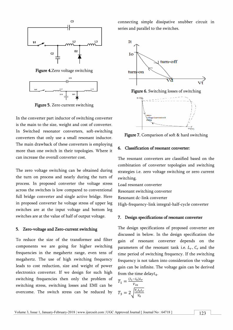
Figure 6. Switching losses of switching
Figure 7. Comparison of soft & hard switching
6. Classification of resonant converter:
The resonant converters are classified based on the
combination of converter topologies and switching
strategies i.e. zero voltage switching or zero current
switching.
Load resonant converter
Resonant switching converter
Resonant dc-link converter
High-frequency-link integral-half-cycle converter
7. Design specifications of resonant converter
The design specifications of proposed converter are
discussed in below. In the design specification the
gain of resonant converter depends on the
parameters of the resonant tank i.e. , and the
time period of switching frequency. If the switching
frequency is not taken into consideration the voltage
gain can be infinite. The voltage gain can be derived
from the time delay .
( )
√

Volume 3, Issue 1, January-February-2018 | www.ijsrcseit.com | UGC Approved Journal [ Journal No : 64718 ]
124
(
)
The voltage gain can be derived from the equation
and it will depend on the resonant frequency and
time period.
( )
Where resonant frequency is given as
√
From the above equation the value of resonant
inductor is given in below equation and resonant
capacitor valve is obtained from resonant inductor or
can be obtained from the voltage gain equation. The
duty ratio for the switches can be obtained from
resonant frequency and the minimum and maximum
values of duty ratio are given in below equation.
( )
( )
9. Operation of resonant step-up converter
The proposed resonant step-up converter consists of
full-bridge converter in which four switches are used,
LC parallel resonant tank and a voltage doubler
circuit and two input blocking diodes. In proposed
resonant step-up converter the high gain can be
obtained by resonant tank impedance. When the
resonant inductor and resonant capacitors are in
resonance then the maximum gain can be obtained.
The operation of proposed converter also depends on
the resonant frequency and switching frequency .
In proposed converter the switches Q1 and Q4 can
be turned-on and turned-off simultaneously. The
fallowing assumptions are made in order to simplify
the analysis:
The components that are used in the converter
operation are ideal i.e. all switches, diodes, inductor
and capacitors.
In proposed converter the output filter capacitors
that are used in operation are large enough to meet
the output voltage during the switching period.
The structure of proposed converter is shown in
below fig: 8. The operational modes are explained in
the fallowing stages.
Figure 8. Topological structure of the proposed
resonant step-up converter
Mode (1): During this mode of operation the
switches S1 and S4 are trigged using gate pulse. And
the current flows through the S1, resonant inductor
and S4 to complete the operation. The positive input
voltage is appeared across the LC parallel resonant
tank. In this mode the converter operates similar to
the boost converter and the resonant inductor acts
boost inductor as like boost converter. The below
fig:9 the mode 1 operation.
Figure 9. Mode-1 Operation
The current through the resonant inductor starts
linearly from the steady state value . In this mode
the load is powered by the output filter capacitors.
After the completion of this mode the resonant
converter is given as
In this mode the energy transferred is given as
(
)

Volume 3, Issue 1, January-February-2018 | www.ijsrcseit.com | UGC Approved Journal [ Journal No : 64718 ]
125
Mode (2): During this mode the switches
and are turned off at zero voltage and after that the
resonant inductor resonates with resonant
capacitor . The resonant capacitor voltage
decrease from input voltage and the resonant
inductor current increase from in resonant form.
For better understanding of the converter during this
mode consider parasitic output capacitors of
through , the junction capacitor of blocking diode
and the equivalent circuit after is shown in
below fig: 10.
Figure 10. Equivalent Circuit of Mode 2
From the above fig:10 the capacitors , and
are charged where as the rest of the capacitors are
discharged. To realise zero voltage switching for
and an additional capacitor is connected in
parallel with respect to and the value of the
capacitor is ten times the value of the capacitor .
The value of resonant capacitor is much larger
than parasitic capacitances; hence the voltage across
the switch and increase slowly. So the switches
S1 and S4 are turned off at almost zero voltage in this
mode.
When the voltage across the resonant capacitor
decrease to zero then the resonant inductor current
reaches to its maximum magnitude. After that
resonant capacitor voltage increase in negative
direction and declines in resonant form.
Figure 11. Equivalent Circuit of Mode 3
At time period and the voltage across
switch and reaches to input voltage as a
result the voltage across , fall to zero and it can
be turned on under ZVS condition.As the switches ,
are turned on but there is current flowing through
them because the gate pulse is not triggered. After
the resonant inductor is continues to resonate with
resonant capacitor and the voltage across keep
on increase in negative direction. The voltage across
the switch is continues to increase from to half
of the output voltage and the switch voltage across
is kept at the input voltage .
Figure 12. Mode-2 Operations
From the above fig: 12 the voltage stress across is
at input voltage and the voltage stress across is the
value of half of output voltage. During this mode no

Volume 3, Issue 1, January-February-2018 | www.ijsrcseit.com | UGC Approved Journal [ Journal No : 64718 ]
126
power transfer from input source to load and whole
energy is stored in LC resonant tank. The fallowing
equations represent the flow of power.
(
)
( )
[( ) ] [( ) ]
( ) [( ) ] [( ) ]
Where
√
Mode (3): In this mode the triggering pulse is given
to the switches and . The inductor current
decrease in negative direction. The resonant
capacitor voltage increase in positive direction.
The switch voltages in this mode is given as across
the switch is input voltage and voltage across the
switch is the half of the output voltage. Therefore
the voltage stresses across the switches are input
voltage and half of output voltage.
Figure 13. Mode-3 Operations
The fig: 13 show the mode of operation. The voltage
across the output capacitors are the half of the output
voltages. The voltage doubler circuit doubles the
voltage of .
Mode (4): In this mode of operation the switch
and are turned off by zero voltage switching
condition. The inductor is resonant with the
capacitor and the stored energy is delivered to the
load. In this mode the current flows through the
and to the load capacitors.
The voltage across the output capacitors are not equal
i.e. because the average current flowing
into will be higher than the average current
flowing through the and vice versa. The capacitor
and share the same power hence decrease
and increases and finally they will share the same
output voltage.
Figure 14. Mode-4 operation
From the above fig it is clear that the power flow to
the load is fed by the stored energy in the LC
resonant tank.
III. RESULTS AND DISCUSSION
Experimental Results
The hardware components specification and its
rating given in the Table: and these specifications are
the maximum ratings of the component and the
storage components inductor and capacitor are the
critical values of converter. These specifications and
components are given based on the design of
converter.
Gate Drive Circuit
Fig: 15 shows the circuit diagram of gate drive circuit
for switches used in proposed converter. MOSFETs
are voltage-controlled devices and very high input
impedance. The gate draws a very small leakage
current, in the order of nanoamperes. The turn on
time of an MOSFET depends on the charging time of
input or gate capacitance.
The gating circuit is an integral part of a power
converter that consist of power semi-conductor
devices. The output of a converter depends on how
the gating circuit drives the switching devices is a

Volume 3, Issue 1, January-February-2018 | www.ijsrcseit.com | UGC Approved Journal [ Journal No : 64718 ]
127
direct function of switching. Therefore, the
characteristics of the gating circuit are key elements
in achieving the desired output and the control
requirements of any power converter.
The design of a gating circuit requires knowledge of
gate characteristics and needs of device such as
thyristors, bipolar transistors, and MOSFETs. Because
power electronics are increasingly used in
applications that require gate drive circuits with
advance control, high speed, high efficiency, and
compactness, gate driver integrated circuits are
becoming commercially available.
Figure 15. Gate driver circuit for switches
The hardware implementation of gate drive circuit
shown in Fig:15 and circuit uses to boost the supply
voltage for turning on the MOSEFET using PIC kit
and connected directly to the gate terminal of the
switch as shown in Fig: 4.6.
Figure 16. Hardware implementation of gate driver
circuit
The below fig:16 show the experimental set up of a
resonant step-up converter. In the diagram testing of
a circuit by the PIC micro controller for the
generation of pulse to trigger the main switches.
Figure 17. Hardware implementation of proposed
converter
The fig:17 represent the input voltage and output
voltage waveforms. In this waveform when the input
voltage is given to converter and the gain obtained is
eight times greater than the input voltage. The pulse
is given to the switches with the 30% duty ratio so
that the control of the circuit is easy.
Figure 18. Input and Output voltage of converter
Figure 19. Input voltage and current of converter

Volume 3, Issue 1, January-February-2018 | www.ijsrcseit.com | UGC Approved Journal [ Journal No : 64718 ]
128
Figure 20. resonant inductor current of the converter
IV. CONCLUSION
A novel step-up resonant converter is suggested in
this paper, which can achieve high voltage gain
through the parallel LC resonant tank and it is well
suitable for high-power high-voltage applications.
The converter uses the resonant inductor to deliver
power as that of boost converter. The resonant
inductor charges from the input and discharges at the
output. To achieve zero voltage switching during
turn-on, turn-off for the active switches and zero
current switching for rectifier diode the resonant
capacitor is employed. From the analysis the
converter can operate at any gain (>2) with proper
control of active switch. The maximum switching
frequency of the converter can be achieved from the
parameters of resonant tank. And it also determines
the range of switching frequency and current ratings
of active switches and diodes. The proposed resonant
converter is operated at constant switching
frequency. The operation principle and selection of
resonant parameters can be verified by simulation
and experimental results.
V. REFERENCES
[1]. CIGER B4-52 working group, HVDC grid
feasibility study. Melbourne, vic. Australia : int.
council large electer.syst2011.
[2]. A.S.Abdel-khalik, A.M.massoud A.A elserougi,
and s.ahmed, "optimum power transmission
based droop control deasignfor multi – terminal
HVDC of offshore wind farms ", IEEE trans.
Power system.vol 28, no.3, pp. 3401-3409, aug
2013.
[3]. Jovic "Bidirectional, high power DC
Transformer", IEEE Trans.Power Del.VOL.24,
no.4, pp.2276-2283, oct 2009.
[4]. C.Zhan, A.Bullock, C.Smith and A.Crane,
"Power collection and transmission systems" Eur
Patent apple.EP2341594A1, 2011.
[5]. C Mayer "key components for future offshore
DC grids", Ph.D.Dissertation, RWTH Aachen
Uni..Asachen, Germany pp 9-12-2007.
[6]. K.Stephen " Moduler DC/DC converter for DC
distribution and collection networks" Ph.D
dissertation.EPFL Lausanne, Switzerland .pp.81-
94-2012.