dc-dc converter control circuits - st.com · dc-dc converter control circuits datasheet -production...
TRANSCRIPT
This is information on a product in full production.
April 2013 DocID5257 Rev 11 1/23
23
MC34063AB, MC34063AC, MC34063EB, MC34063EC
DC-DC converter control circuits
Datasheet - production data
Features
Output switch current in excess of 1.5 A
2 % reference accuracy
Low quiescent current: 2.5 mA (typ.)
Operating from 3 V to 40 V
Frequency operation to 100 kHz
Active current limiting
Description
The MC34063A/E series is a monolithic control circuit which delivers the main functions for DC-DC voltage converting.
The device contains an internal temperature compensated reference, comparator, duty cycle controlled oscillator with an active current limit circuit, driver and high current output switch. Output voltage is adjustable through two external resistors with a 2% reference accuracy.
Employing a minimum number of external components, the MC34063A/E device series is designed for step-down, step-up and voltage-inverting applications.
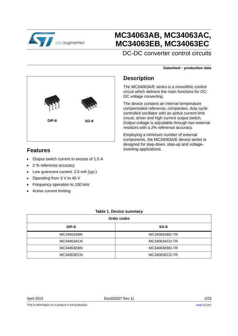
SO-8DIP-8
Table 1. Device summary
Order codes
DIP-8 SO-8
MC34063ABN MC34063ABD-TR
MC34063ACN MC34063ACD-TR
MC34063EBN MC34063EBD-TR
MC34063ECN MC34063ECD-TR
www.st.com
Contents MC34063AB, MC34063AC, MC34063EB, MC34063EC
2/23 DocID5257 Rev 11
Contents
1 Diagram . . . . . . . . . . . . . . . . . . . . . . . . . . . . . . . . . . . . . . . . . . . . . . . . . . . 3
2 Pin configuration . . . . . . . . . . . . . . . . . . . . . . . . . . . . . . . . . . . . . . . . . . . . 4
3 Maximum ratings . . . . . . . . . . . . . . . . . . . . . . . . . . . . . . . . . . . . . . . . . . . . 5
4 Electrical characteristics . . . . . . . . . . . . . . . . . . . . . . . . . . . . . . . . . . . . . 6
5 Typical performance characteristics . . . . . . . . . . . . . . . . . . . . . . . . . . . . 8
6 Typical application circuit . . . . . . . . . . . . . . . . . . . . . . . . . . . . . . . . . . . 10
7 Package mechanical data . . . . . . . . . . . . . . . . . . . . . . . . . . . . . . . . . . . . 18
8 Revision history . . . . . . . . . . . . . . . . . . . . . . . . . . . . . . . . . . . . . . . . . . . 22
DocID5257 Rev 11 3/23
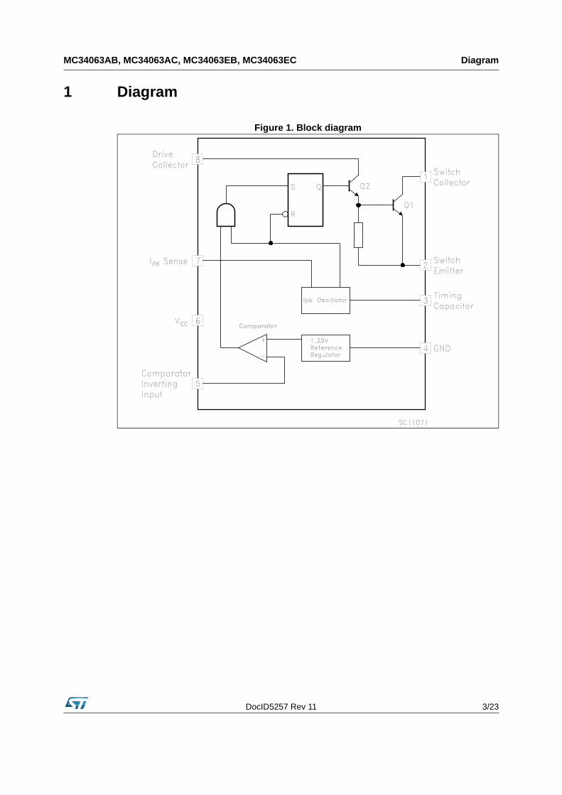
MC34063AB, MC34063AC, MC34063EB, MC34063EC Diagram
1 Diagram
Figure 1. Block diagram
Pin configuration MC34063AB, MC34063AC, MC34063EB, MC34063EC
4/23 DocID5257 Rev 11
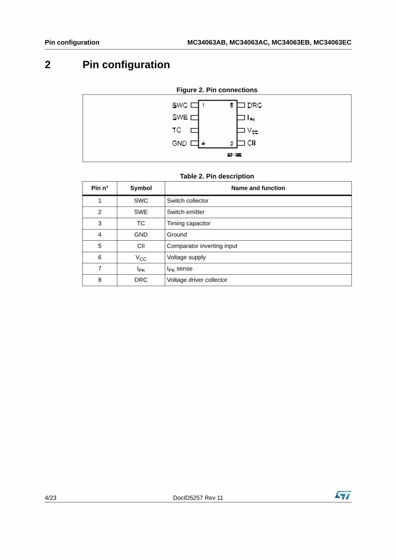
2 Pin configuration
Figure 2. Pin connections
Table 2. Pin description
Pin n° Symbol Name and function
1 SWC Switch collector
2 SWE Switch emitter
3 TC Timing capacitor
4 GND Ground
5 CII Comparator inverting input
6 VCC Voltage supply
7 IPK IPK sense
8 DRC Voltage driver collector
DocID5257 Rev 11 5/23
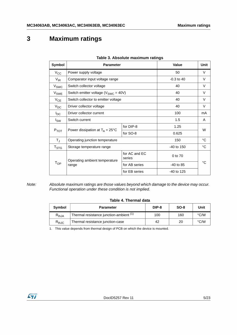
MC34063AB, MC34063AC, MC34063EB, MC34063EC Maximum ratings
3 Maximum ratings
Note: Absolute maximum ratings are those values beyond which damage to the device may occur. Functional operation under these condition is not implied.
Table 3. Absolute maximum ratings
Symbol Parameter Value Unit
VCC Power supply voltage 50 V
VIR Comparator input voltage range -0.3 to 40 V
VSWC Switch collector voltage 40 V
VSWE Switch emitter voltage (VSWC = 40V) 40 V
VCE Switch collector to emitter voltage 40 V
VDC Driver collector voltage 40 V
IDC Driver collector current 100 mA
ISW Switch current 1.5 A
PTOT Power dissipation at TA = 25°Cfor DIP-8 1.25
Wfor SO-8 0.625
TJ Operating junction temperature 150 °C
TSTG Storage temperature range -40 to 150 °C
TOPOperating ambient temperature range
for AC and EC series
0 to 70
°Cfor AB series -40 to 85
for EB series -40 to 125
Table 4. Thermal data
Symbol Parameter DIP-8 SO-8 Unit
RthJA Thermal resistance junction-ambient (1)
1. This value depends from thermal design of PCB on which the device is mounted.
100 160 °C/W
RthJC Thermal resistance junction-case 42 20 °C/W

Electrical characteristics MC34063AB, MC34063AC, MC34063EB, MC34063EC
6/23 DocID5257 Rev 11
4 Electrical characteristics
Refer to the test circuits, VCC = 5 V, TA = TLOW to THIGH, unless otherwise specified. (a)
a. TLOW = 0 °C, THIGH = 70 °C (AC and EC series); TLOW = -40 °C, THIGH = 85 °C (AB series); TLOW = -40 °C, THIGH = 125 °C (EB series)
Table 5. Oscillator
Symbol Parameter Test conditions Min. Typ. Max. Unit
fOSC Frequency VPIN5 = 0V, CT = 1 nF, TA = 25°C 24 33 42 kHz
ICHG Charge current VCC = 5 to 40V, TA = 25°C 24 33 42 µA
IDISCHG Discharge current VCC = 5 to 40V, TA = 25°C 140 200 260 µA
IDISCHG/ICHGDischarge to charge current ratio
PIN 7 = VCC, TA = 25°C 5.2 6.2 7.5 µA
VIPK(sense) Current limit sense voltage ICHG = IDISCHG, TA = 25°C 250 300 350 mV
Table 6. Output switch
Symbol Parameter Test conditions Min. Typ. Max. Unit
VCE(sat)Saturation voltage, Darlington connection
ISW = 1 A, PIN 1, 8 connected 1 1.3 V
VCE(sat) Saturation voltageISW = 1 A, RPIN8 = 82 to VCCForced ~ 20
0.45 0.7 V
hFE DC current gain ISW = 1 A,VCE = 5 V, TA = 25°C 50 120
IC(off) Collector off-state current VCE = 40 V 0.01 100 µA
Table 7. Comparator
Symbol Parameter Test conditions Min. Typ. Max. Unit
VTH Threshold voltageTA = 25°C 1.225 1.25 1.275
VTA = TLOW to THIGH 1.21 1.29
ReglineThreshold voltage line regulation
VCC = 3 to 40 V 1 5 mV
IIB Input bias current VIN = 0 V -5 -400 nA
DocID5257 Rev 11 7/23
MC34063AB, MC34063AC, MC34063EB, MC34063EC Electrical characteristics
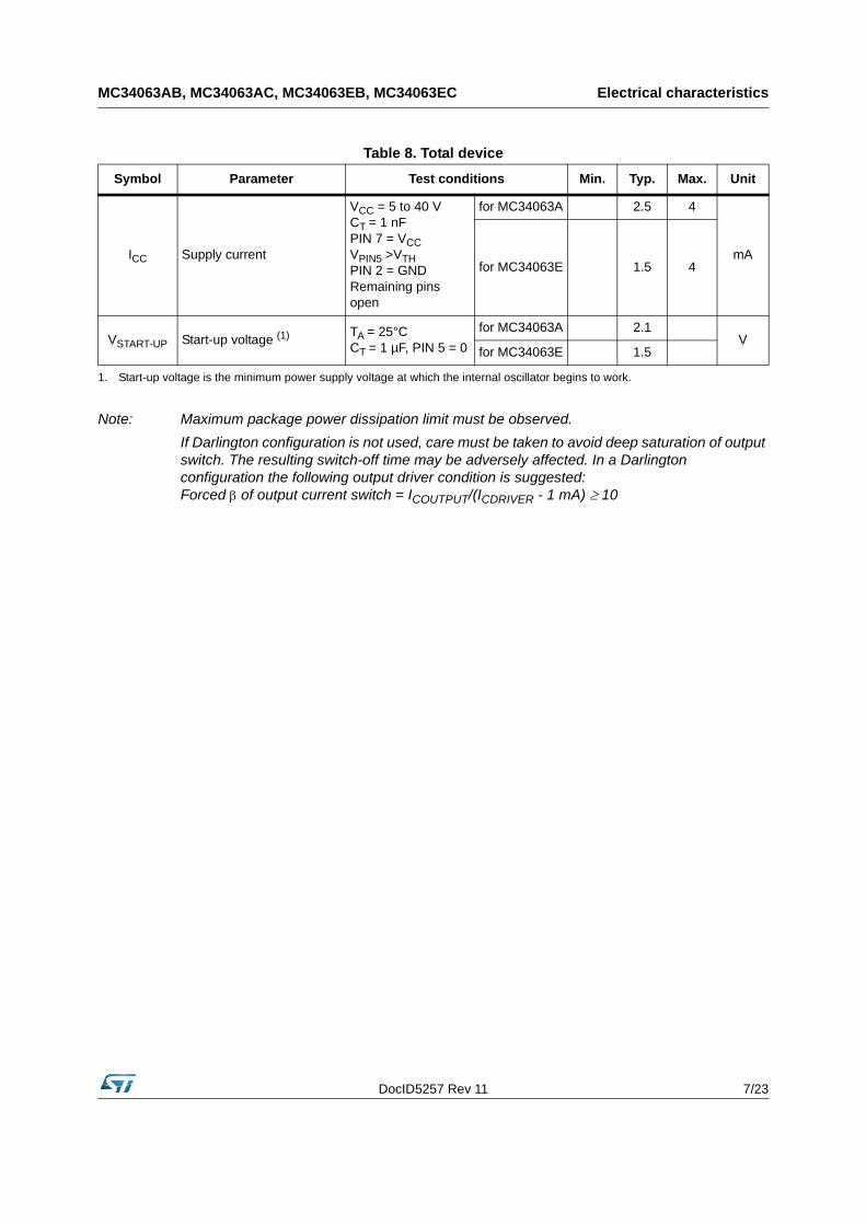
Note: Maximum package power dissipation limit must be observed.
If Darlington configuration is not used, care must be taken to avoid deep saturation of output switch. The resulting switch-off time may be adversely affected. In a Darlington configuration the following output driver condition is suggested:Forced of output current switch = ICOUTPUT/(ICDRIVER - 1 mA) 10
Table 8. Total device
Symbol Parameter Test conditions Min. Typ. Max. Unit
ICC Supply current
VCC = 5 to 40 VCT = 1 nFPIN 7 = VCCVPIN5 >VTHPIN 2 = GNDRemaining pins open
for MC34063A 2.5 4
mA1.5 4for MC34063E
VSTART-UP Start-up voltage (1) TA = 25°CCT = 1 µF, PIN 5 = 0
for MC34063A 2.1V
for MC34063E 1.5
1. Start-up voltage is the minimum power supply voltage at which the internal oscillator begins to work.
Typical performance characteristics MC34063AB, MC34063AC, MC34063EB, MC34063EC
8/23 DocID5257 Rev 11
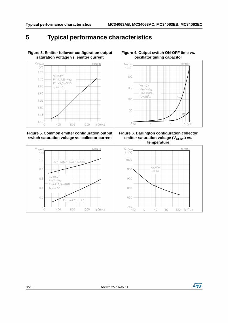
5 Typical performance characteristics
Figure 3. Emitter follower configuration output saturation voltage vs. emitter current
Figure 4. Output switch ON-OFF time vs. oscillator timing capacitor
Figure 5. Common emitter configuration output switch saturation voltage vs. collector current
Figure 6. Darlington configuration collector emitter saturation voltage (VCEsat) vs.
temperature
DocID5257 Rev 11 9/23
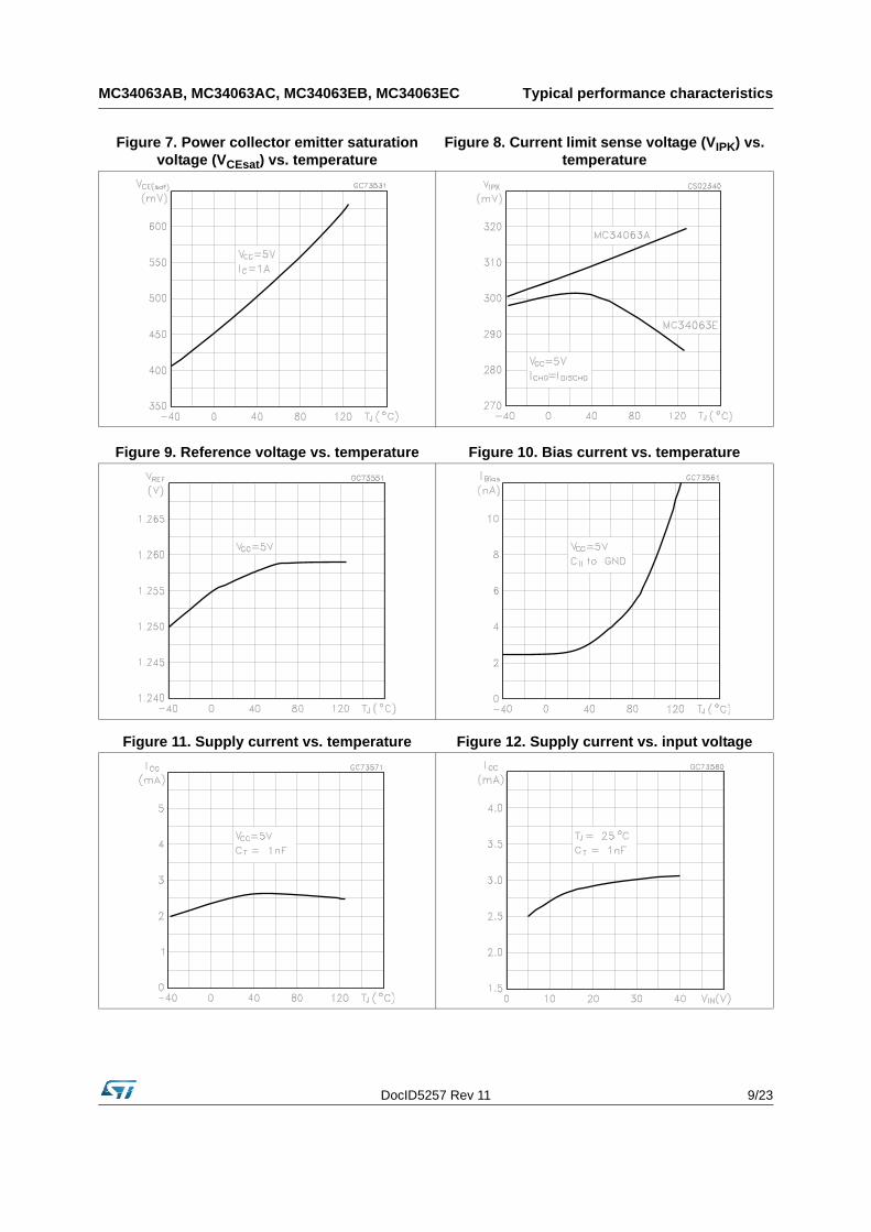
MC34063AB, MC34063AC, MC34063EB, MC34063EC Typical performance characteristics
Figure 7. Power collector emitter saturation voltage (VCEsat) vs. temperature
Figure 8. Current limit sense voltage (VIPK) vs. temperature
Figure 9. Reference voltage vs. temperature Figure 10. Bias current vs. temperature
Figure 11. Supply current vs. temperature Figure 12. Supply current vs. input voltage
Typical application circuit MC34063AB, MC34063AC, MC34063EB, MC34063EC
10/23 DocID5257 Rev 11
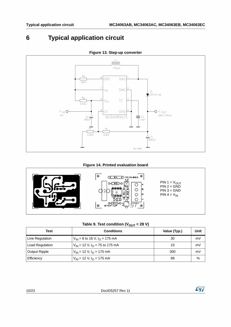
6 Typical application circuit
Figure 13. Step-up converter
Figure 14. Printed evaluation board
PIN 1 = VOUTPIN 2 = GNDPIN 3 = GNDPIN 4 = VIN
Table 9. Test condition (VOUT = 28 V)
Test Conditions Value (Typ.) Unit
Line Regulation VIN = 8 to 16 V, IO = 175 mA 30 mV
Load Regulation VIN = 12 V, IO = 75 to 175 mA 10 mV
Output Ripple VIN = 12 V, IO = 175 mA 300 mV
Efficiency VIN = 12 V, IO = 175 mA 89 %
DocID5257 Rev 11 11/23
MC34063AB, MC34063AC, MC34063EB, MC34063EC Typical application circuit
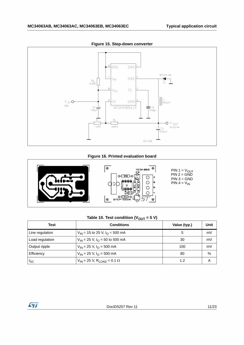
Figure 15. Step-down converter
Figure 16. Printed evaluation board
PIN 1 = VOUTPIN 2 = GNDPIN 3 = GNDPIN 4 = VIN
Table 10. Test condition (VOUT = 5 V)
Test Conditions Value (typ.) Unit
Line regulation VIN = 15 to 25 V, IO = 500 mA 5 mV
Load regulation VIN = 25 V, IO = 50 to 500 mA 30 mV
Output ripple VIN = 25 V, IO = 500 mA 100 mV
Efficiency VIN = 25 V, IO = 500 mA 80 %
ISC VIN = 25 V, RLOAD = 0.1 1.2 A
Typical application circuit MC34063AB, MC34063AC, MC34063EB, MC34063EC
12/23 DocID5257 Rev 11
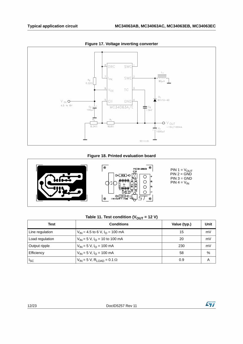
Figure 17. Voltage inverting converter
Figure 18. Printed evaluation board
PIN 1 = VOUTPIN 2 = GNDPIN 3 = GNDPIN 4 = VIN
Table 11. Test condition (VOUT = 12 V)
Test Conditions Value (typ.) Unit
Line regulation VIN = 4.5 to 6 V, IO = 100 mA 15 mV
Load regulation VIN = 5 V, IO = 10 to 100 mA 20 mV
Output ripple VIN = 5 V, IO = 100 mA 230 mV
Efficiency VIN = 5 V, IO = 100 mA 58 %
ISC VIN = 5 V, RLOAD = 0.1 0.9 A
DocID5257 Rev 11 13/23
MC34063AB, MC34063AC, MC34063EB, MC34063EC Typical application circuit
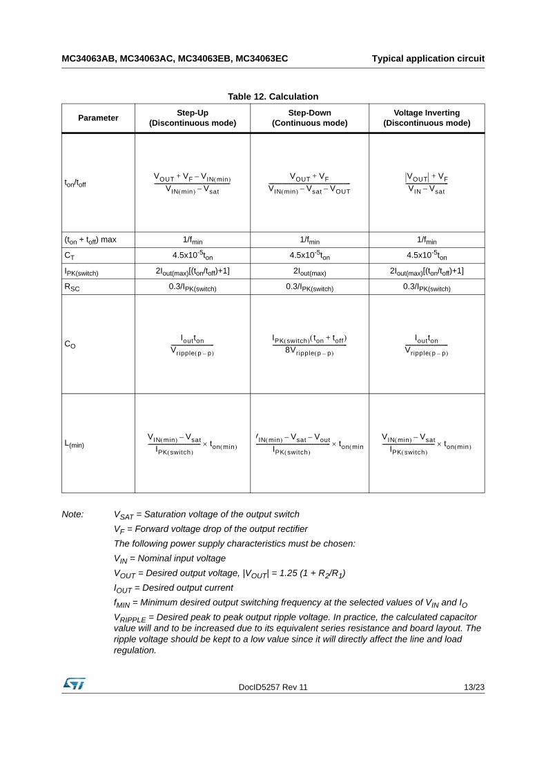
Note: VSAT = Saturation voltage of the output switch
VF = Forward voltage drop of the output rectifier
The following power supply characteristics must be chosen:
VIN = Nominal input voltage
VOUT = Desired output voltage, |VOUT| = 1.25 (1 + R2/R1)
IOUT = Desired output current
fMIN = Minimum desired output switching frequency at the selected values of VIN and IOVRIPPLE = Desired peak to peak output ripple voltage. In practice, the calculated capacitor value will and to be increased due to its equivalent series resistance and board layout. The ripple voltage should be kept to a low value since it will directly affect the line and load regulation.
Table 12. Calculation
ParameterStep-Up
(Discontinuous mode)Step-Down
(Continuous mode)Voltage Inverting
(Discontinuous mode)
ton/toff
(ton + toff) max 1/fmin 1/fmin 1/fmin
CT 4.5x10⁻⁵ton 4.5x10⁻⁵ton 4.5x10⁻⁵ton
IPK(switch) 2Iout(max)[(ton/toff)+1] 2Iout(max) 2Iout(max)[(ton/toff)+1]
RSC 0.3/IPK(switch) 0.3/IPK(switch) 0.3/IPK(switch)
CO
L(min)
VOUT VF VIN min –+
VIN min Vsat–-------------------------------------------------------
VOUT VF+
VIN min Vsat– VOUT–-----------------------------------------------------------
VOUT VF+
VIN Vsat–-------------------------------
Ioutton
Vripple p p– -------------------------------
IPK switch ton toff+ 8Vripple p p–
------------------------------------------------------Ioutton
Vripple p p– -------------------------------
VIN min Vsat–
IPK switch -------------------------------------- ton min
VIN min Vsat– Vout–
IPK switch ------------------------------------------------------- ton min
VIN min Vsat–
IPK switch -------------------------------------- ton min
Typical application circuit MC34063AB, MC34063AC, MC34063EB, MC34063EC
14/23 DocID5257 Rev 11
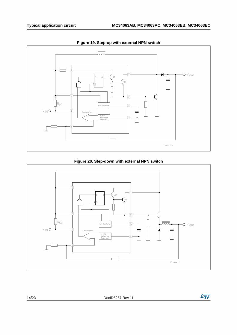
Figure 19. Step-up with external NPN switch
Figure 20. Step-down with external NPN switch
DocID5257 Rev 11 15/23
MC34063AB, MC34063AC, MC34063EB, MC34063EC Typical application circuit
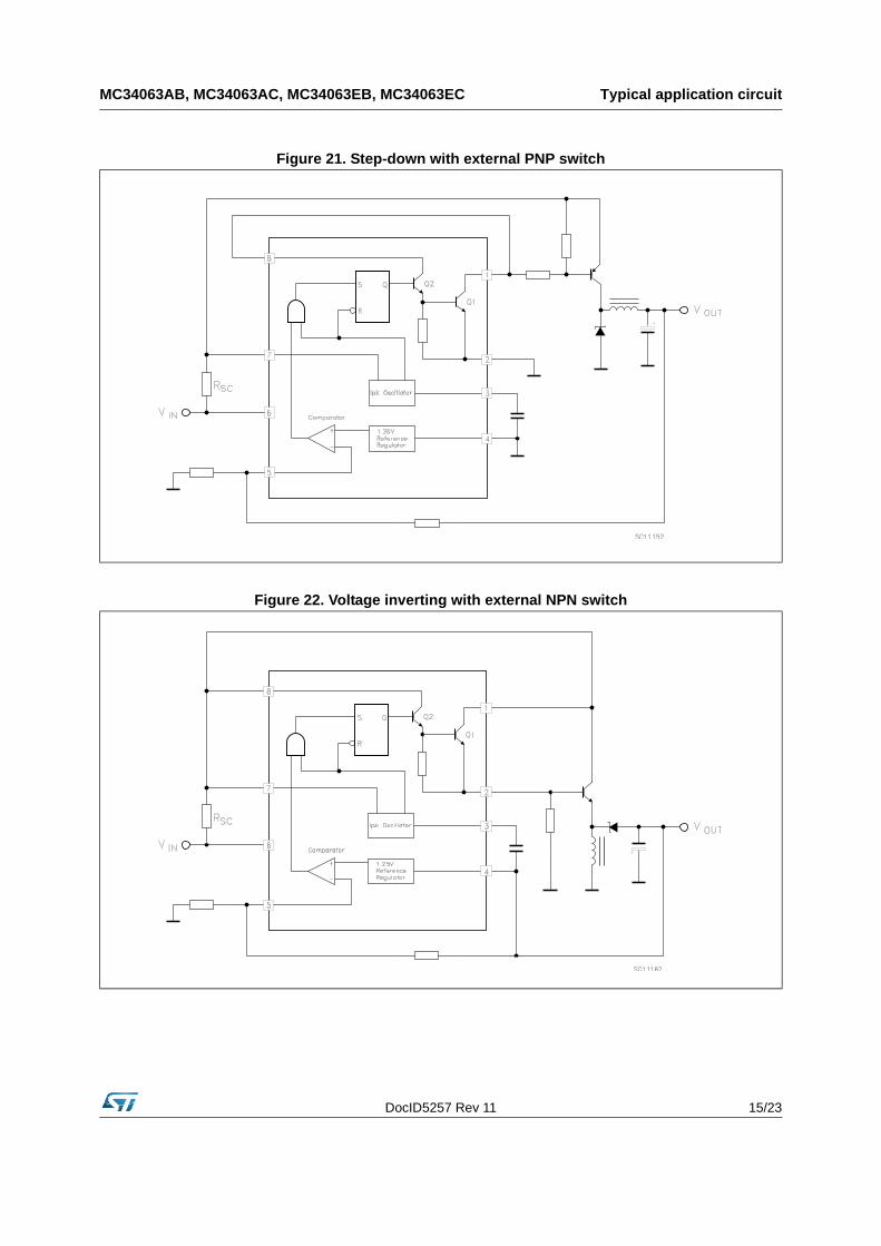
Figure 21. Step-down with external PNP switch
Figure 22. Voltage inverting with external NPN switch
Typical application circuit MC34063AB, MC34063AC, MC34063EB, MC34063EC
16/23 DocID5257 Rev 11
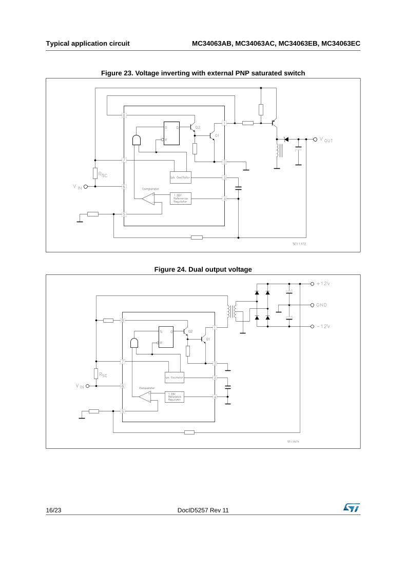
Figure 23. Voltage inverting with external PNP saturated switch
Figure 24. Dual output voltage
DocID5257 Rev 11 17/23
MC34063AB, MC34063AC, MC34063EB, MC34063EC Typical application circuit
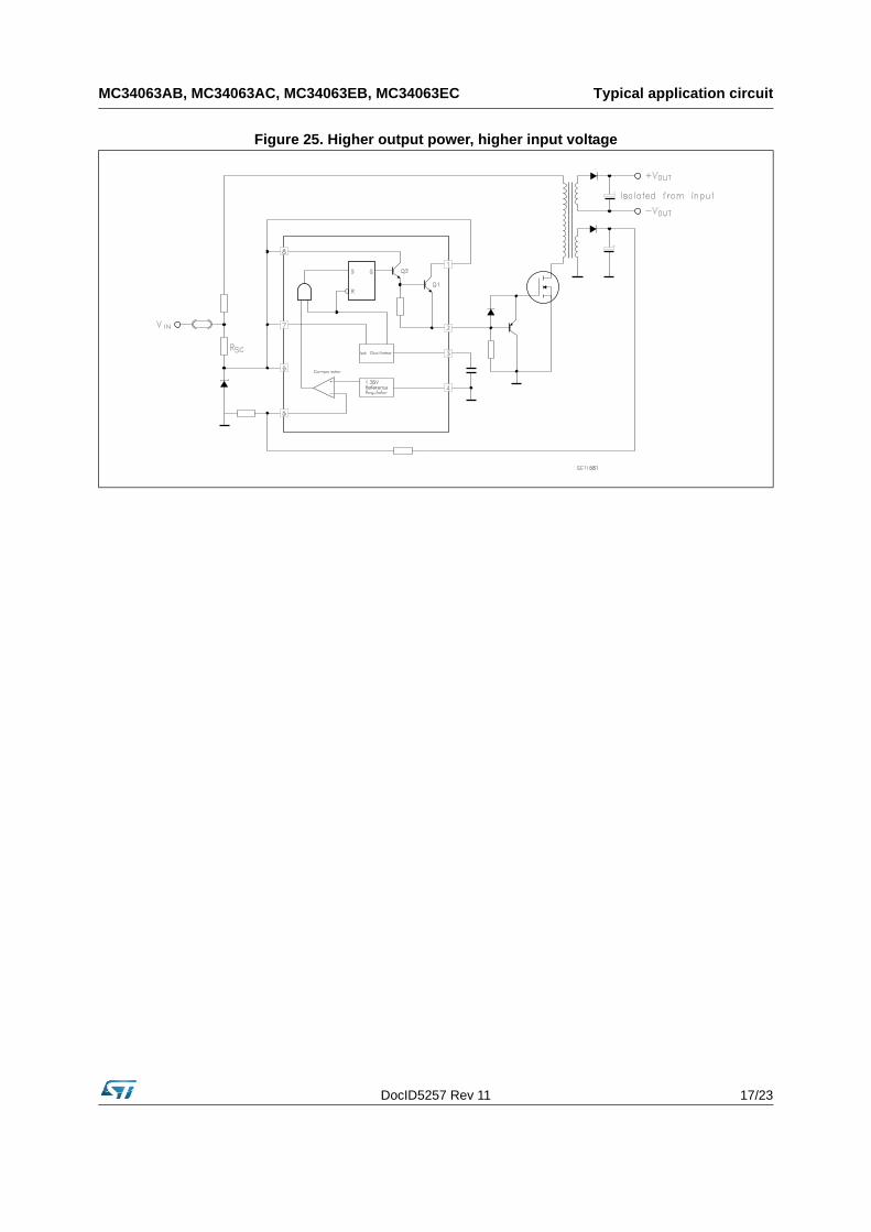
Figure 25. Higher output power, higher input voltage
Package mechanical data MC34063AB, MC34063AC, MC34063EB, MC34063EC
18/23 DocID5257 Rev 11
7 Package mechanical data
In order to meet environmental requirements, ST offers these devices in different grades of ECOPACK® packages, depending on their level of environmental compliance. ECOPACK® specifications, grade definitions and product status are available at: www.st.com. ECOPACK® is an ST trademark.
DocID5257 Rev 11 19/23
MC34063AB, MC34063AC, MC34063EB, MC34063EC Package mechanical data
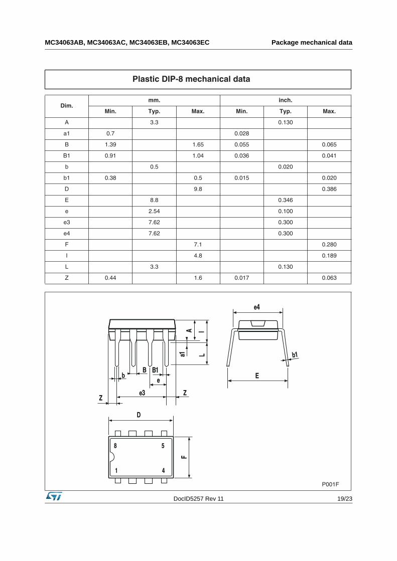
Dim.mm. inch.
Min. Typ. Max. Min. Typ. Max.
A 3.3 0.130
a1 0.7 0.028
B 1.39 1.65 0.055 0.065
B1 0.91 1.04 0.036 0.041
b 0.5 0.020
b1 0.38 0.5 0.015 0.020
D 9.8 0.386
E 8.8 0.346
e 2.54 0.100
e3 7.62 0.300
e4 7.62 0.300
F 7.1 0.280
I 4.8 0.189
L 3.3 0.130
Z 0.44 1.6 0.017 0.063
Plastic DIP-8 mechanical data
P001F
Package mechanical data MC34063AB, MC34063AC, MC34063EB, MC34063EC
20/23 DocID5257 Rev 11
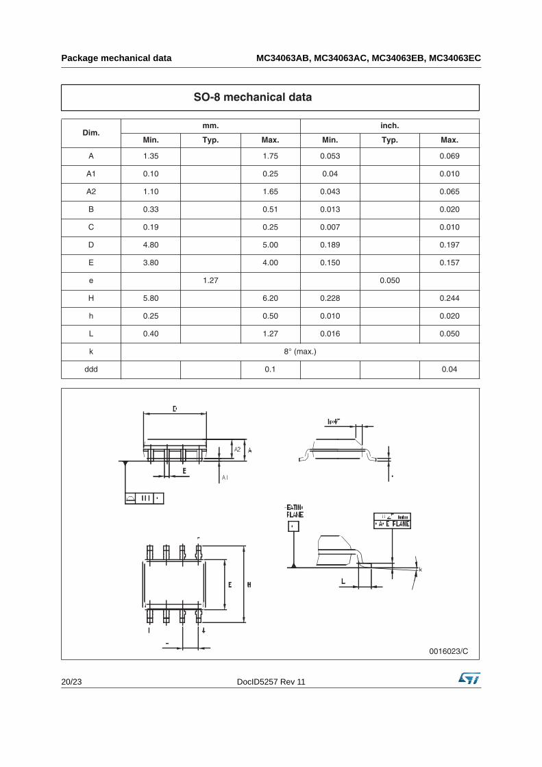
Dim.mm. inch.
Min. Typ. Max. Min. Typ. Max.
A 1.35 1.75 0.053 0.069
A1 0.10 0.25 0.04 0.010
A2 1.10 1.65 0.043 0.065
B 0.33 0.51 0.013 0.020
C 0.19 0.25 0.007 0.010
D 4.80 5.00 0.189 0.197
E 3.80 4.00 0.150 0.157
e 1.27 0.050
H 5.80 6.20 0.228 0.244
h 0.25 0.50 0.010 0.020
L 0.40 1.27 0.016 0.050
k 8° (max.)
ddd 0.1 0.04
SO-8 mechanical data
0016023/C
DocID5257 Rev 11 21/23
MC34063AB, MC34063AC, MC34063EB, MC34063EC Package mechanical data
Dim.mm. inch.
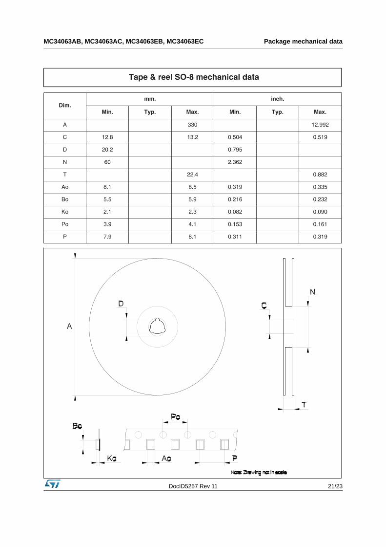
Min. Typ. Max. Min. Typ. Max.
A 330 12.992
C 12.8 13.2 0.504 0.519
D 20.2 0.795
N 60 2.362
T 22.4 0.882
Ao 8.1 8.5 0.319 0.335
Bo 5.5 5.9 0.216 0.232
Ko 2.1 2.3 0.082 0.090
Po 3.9 4.1 0.153 0.161
P 7.9 8.1 0.311 0.319
Tape & reel SO-8 mechanical data
Revision history MC34063AB, MC34063AC, MC34063EB, MC34063EC
22/23 DocID5257 Rev 11
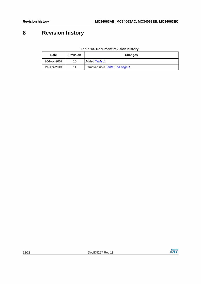
8 Revision history
Table 13. Document revision history
Date Revision Changes
20-Nov-2007 10 Added Table 1.
24-Apr-2013 11 Removed note Table 1 on page 1.
DocID5257 Rev 11 23/23
MC34063AB, MC34063AC, MC34063EB, MC34063EC
Please Read Carefully:
Information in this document is provided solely in connection with ST products. STMicroelectronics NV and its subsidiaries (“ST”) reserve theright to make changes, corrections, modifications or improvements, to this document, and the products and services described herein at anytime, without notice.
All ST products are sold pursuant to ST’s terms and conditions of sale.
Purchasers are solely responsible for the choice, selection and use of the ST products and services described herein, and ST assumes noliability whatsoever relating to the choice, selection or use of the ST products and services described herein.
No license, express or implied, by estoppel or otherwise, to any intellectual property rights is granted under this document. If any part of thisdocument refers to any third party products or services it shall not be deemed a license grant by ST for the use of such third party productsor services, or any intellectual property contained therein or considered as a warranty covering the use in any manner whatsoever of suchthird party products or services or any intellectual property contained therein.
UNLESS OTHERWISE SET FORTH IN ST’S TERMS AND CONDITIONS OF SALE ST DISCLAIMS ANY EXPRESS OR IMPLIEDWARRANTY WITH RESPECT TO THE USE AND/OR SALE OF ST PRODUCTS INCLUDING WITHOUT LIMITATION IMPLIEDWARRANTIES OF MERCHANTABILITY, FITNESS FOR A PARTICULAR PURPOSE (AND THEIR EQUIVALENTS UNDER THE LAWSOF ANY JURISDICTION), OR INFRINGEMENT OF ANY PATENT, COPYRIGHT OR OTHER INTELLECTUAL PROPERTY RIGHT.
ST PRODUCTS ARE NOT AUTHORIZED FOR USE IN WEAPONS. NOR ARE ST PRODUCTS DESIGNED OR AUTHORIZED FOR USEIN: (A) SAFETY CRITICAL APPLICATIONS SUCH AS LIFE SUPPORTING, ACTIVE IMPLANTED DEVICES OR SYSTEMS WITHPRODUCT FUNCTIONAL SAFETY REQUIREMENTS; (B) AERONAUTIC APPLICATIONS; (C) AUTOMOTIVE APPLICATIONS ORENVIRONMENTS, AND/OR (D) AEROSPACE APPLICATIONS OR ENVIRONMENTS. WHERE ST PRODUCTS ARE NOT DESIGNEDFOR SUCH USE, THE PURCHASER SHALL USE PRODUCTS AT PURCHASER’S SOLE RISK, EVEN IF ST HAS BEEN INFORMED INWRITING OF SUCH USAGE, UNLESS A PRODUCT IS EXPRESSLY DESIGNATED BY ST AS BEING INTENDED FOR “AUTOMOTIVE,AUTOMOTIVE SAFETY OR MEDICAL” INDUSTRY DOMAINS ACCORDING TO ST PRODUCT DESIGN SPECIFICATIONS.PRODUCTS FORMALLY ESCC, QML OR JAN QUALIFIED ARE DEEMED SUITABLE FOR USE IN AEROSPACE BY THECORRESPONDING GOVERNMENTAL AGENCY.
Resale of ST products with provisions different from the statements and/or technical features set forth in this document shall immediately voidany warranty granted by ST for the ST product or service described herein and shall not create or extend in any manner whatsoever, anyliability of ST.
ST and the ST logo are trademarks or registered trademarks of ST in various countries.Information in this document supersedes and replaces all information previously supplied.
The ST logo is a registered trademark of STMicroelectronics. All other names are the property of their respective owners.
© 2013 STMicroelectronics - All rights reserved
STMicroelectronics group of companies
Australia - Belgium - Brazil - Canada - China - Czech Republic - Finland - France - Germany - Hong Kong - India - Israel - Italy - Japan - Malaysia - Malta - Morocco - Philippines - Singapore - Spain - Sweden - Switzerland - United Kingdom - United States of America
www.st.com