date auo date - beyondinfinite.com lcd datasheet by beyondinfinite.com author: beyondinfinite.com...
TRANSCRIPT
Copyright AU Optronics, Inc. December, 2008 All Rights Reserved. T260XW02 VP - Spec. Ver0.3 0/29 No Reproduction and Redistribution Allowed
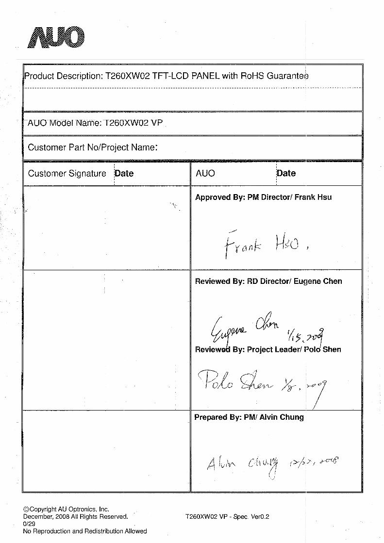
Product Description: T260XW02 TFT-LCD PANEL with RoHS Guarantee
AUO Model Name: T260XW02 VP
Customer Part No/Project Name:
Customer Signature Date AUO Date
Approved By: PM Director/ Frank Hsu
Reviewed By: RD Director/ Eugene Chen
Reviewed By: Project Leader/ Polo Shen
Prepared By: PM/ Alvin Chung
Copyright AU Optronics, Inc. December, 2008 All Rights Reserved. T260XW02 VP - Spec. Ver0.3 1/29 No Reproduction and Redistribution Allowed
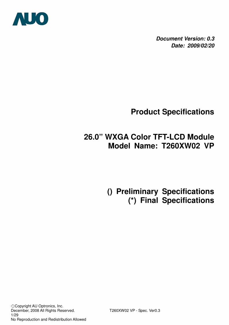
Document Version: 0.3
Date: 2009/02/20
Product Specifications
26.0” WXGA Color TFT-LCD Module Model Name: T260XW02 VP
() Preliminary Specifications (*) Final Specifications
Copyright AU Optronics, Inc. December, 2008 All Rights Reserved. T260XW02 VP - Spec. Ver0.3 2/29 No Reproduction and Redistribution Allowed
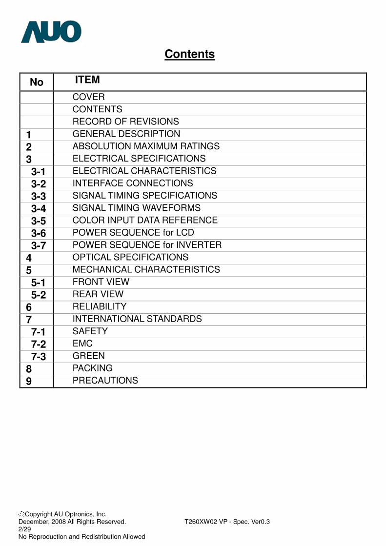
Contents
No ITEM
COVER
CONTENTS
RECORD OF REVISIONS
1 GENERAL DESCRIPTION
2 ABSOLUTION MAXIMUM RATINGS
3 ELECTRICAL SPECIFICATIONS
3-1 ELECTRICAL CHARACTERISTICS
3-2 INTERFACE CONNECTIONS
3-3 SIGNAL TIMING SPECIFICATIONS
3-4 SIGNAL TIMING WAVEFORMS
3-5 COLOR INPUT DATA REFERENCE
3-6 POWER SEQUENCE for LCD
3-7 POWER SEQUENCE for INVERTER
4 OPTICAL SPECIFICATIONS
5 MECHANICAL CHARACTERISTICS
5-1 FRONT VIEW
5-2 REAR VIEW
6 RELIABILITY
7 INTERNATIONAL STANDARDS
7-1 SAFETY
7-2 EMC
7-3 GREEN
8 PACKING
9 PRECAUTIONS
Copyright AU Optronics, Inc. December, 2008 All Rights Reserved. T260XW02 VP - Spec. Ver0.3 3/29 No Reproduction and Redistribution Allowed
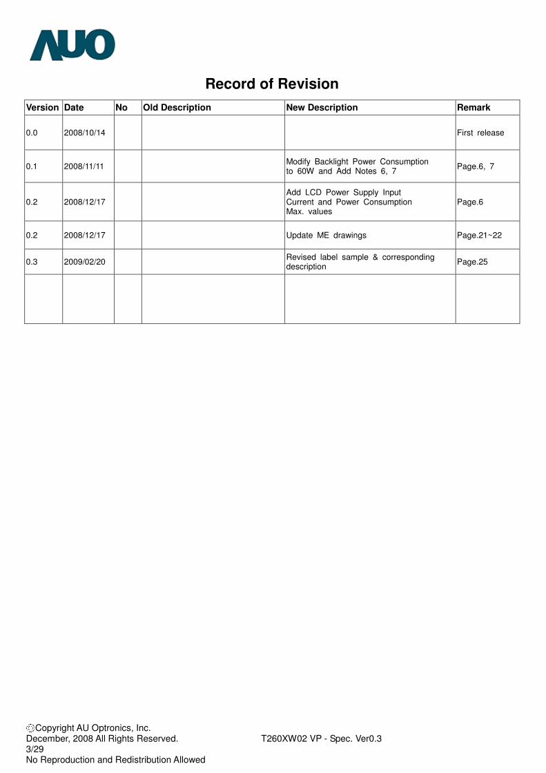
Record of Revision
Version Date No Old Description New Description Remark
0.0 2008/10/14 First release
0.1 2008/11/11 Modify Backlight Power Consumption to 60W and Add Notes 6, 7
Page.6, 7
0.2 2008/12/17 Add LCD Power Supply Input Current and Power Consumption Max. values
Page.6
0.2 2008/12/17 Update ME drawings Page.21~22
0.3 2009/02/20 Revised label sample & corresponding description
Page.25
Copyright AU Optronics, Inc. December, 2008 All Rights Reserved. T260XW02 VP - Spec. Ver0.3 4/29 No Reproduction and Redistribution Allowed
1. General Description
This specification applies to the 26.0 inch Color TFT-LCD Module T260XW02 VP. This LCD module
has a TFT active matrix type liquid crystal panel 1366x768 pixels, and diagonal size of 26.0 inch.
This module supports 1366x768 XGA-WIDE mode (Non-interlace).
Each pixel is divided into Red, Green and Blue sub-pixels or dots which are arranged in vertical
stripes. Gray scale or the brightness of the sub-pixel color is determined with a 8-bit gray scale
signal for each dot.
The T260XW02 VP has been designed to apply the 8-bit 1 channel LVDS interface method. It is
intended to support displays where high brightness, wide viewing angle, high color saturation, and
high color depth are very important. The T260XW02 VP model is RoHS verified which can be
distinguished on panel label.
* General Information
Items Specification Unit Note Active Screen Size 26.0 inches
Display Area 575.769 (H) x 323.712(V) mm
Outline Dimension 626.0 (H) x 373.0 (V) x 45.0(D) mm With inverter
Driver Element a-Si TFT active matrix
Display Colors 16.7M Colors
Number of Pixels 1366 x 768 Pixel
Pixel Pitch 0.4215 mm
Pixel Arrangement RGB vertical stripe
Display Mode Normally Black
Surface Treatment AG, Haze=11%, 3H
Copyright AU Optronics, Inc. December, 2008 All Rights Reserved. T260XW02 VP - Spec. Ver0.3 5/29 No Reproduction and Redistribution Allowed
2. Absolute Maximum Ratings
The following are maximum values which, if exceeded, may cause faulty operation or damage to the unit.
Item Symbol Min Max Unit Conditions Logic/LCD Drive Voltage VCC -0.3 13.2 [Volt] Note 1
Input Voltage of Signal Vin -0.3 3.6 [Volt] Note 1
BLU Input Voltage VDDB -0.3 27.0 [Volt] Note 1
BLU Brightness Control Voltage VDIM -0.3 6.0 [Volt] Note 1
Operating Temperature TOP 0 +50 [oC] Note 2
Operating Humidity HOP 10 90 [%RH] Note 2
Storage Temperature TST -20 +60 [oC] Note 2
Storage Humidity HST 10 90 [%RH] Note 2
Panel Surface Temperature PST 65 [oC] Note 3
Note 1: Duration = 1 sec
Note 2: Maximum Wet-Bulb should be 39 and No condensation.
The relative humidity must not exceed 90% non-condensing at temperatures of 40 or less. At temperatures greater
than 40 , the wet bulb temperature must not exceed 39 .
Note 3: Surface temperature is measured at 50 Dry condition.
Copyright AU Optronics, Inc. December, 2008 All Rights Reserved. T260XW02 VP - Spec. Ver0.3 6/29 No Reproduction and Redistribution Allowed
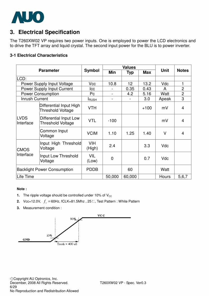
3. Electrical Specification
The T260XW02 VP requires two power inputs. One is employed to power the LCD electronics and to drive the TFT array and liquid crystal. The second input power for the BLU is to power inverter.
3-1 Electrical Characteristics
Values Parameter Symbol Min Typ Max Unit Notes
LCD: Power Supply Input Voltage Vcc 10.8 12 13.2 Vdc 1 Power Supply Input Current Icc - 0.35 0.43 A 2 Power Consumption Pc - 4.2 5.16 Watt 2 Inrush Current IRUSH - - 3.0 Apeak 3
Differential Input High Threshold Voltage
VTH +100 mV 4
Differential Input Low Threshold Voltage
VTL -100 mV 4 LVDS Interface
Common Input Voltage
VCIM 1.10 1.25 1.40 V 4
Input High Threshold Voltage
VIH (High)
2.4 3.3 Vdc CMOS Interface Input Low Threshold
Voltage VIL
(Low) 0 0.7 Vdc
Backlight Power Consumption PDDB 60 Watt
Life Time 50,000 60,000 Hours 5,6,7
Note :
1. The ripple voltage should be controlled under 10% of VCC
2. Vcc=12.0V, =vf 60Hz, fCLK=81.5Mhz , 25 , Test Pattern : White Pattern
3. Measurement condition :
Copyright AU Optronics, Inc. December, 2008 All Rights Reserved. T260XW02 VP - Spec. Ver0.3 7/29 No Reproduction and Redistribution Allowed
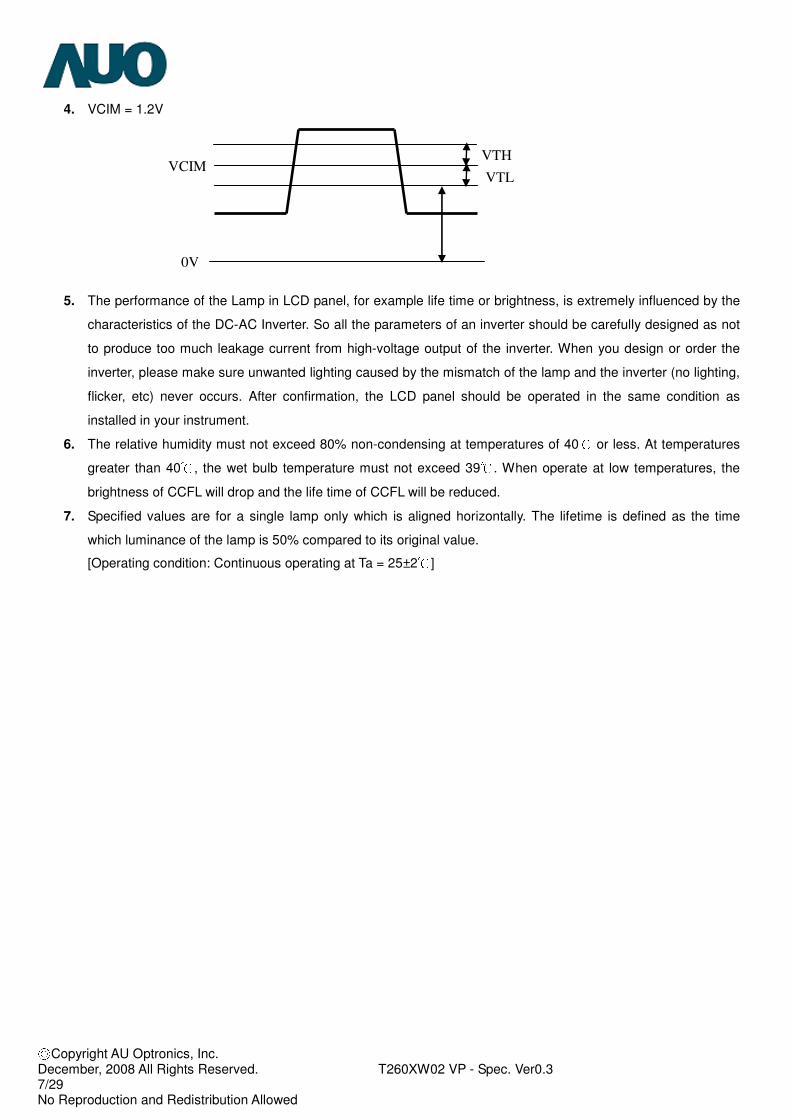
4. VCIM = 1.2V
5. The performance of the Lamp in LCD panel, for example life time or brightness, is extremely influenced by the
characteristics of the DC-AC Inverter. So all the parameters of an inverter should be carefully designed as not
to produce too much leakage current from high-voltage output of the inverter. When you design or order the
inverter, please make sure unwanted lighting caused by the mismatch of the lamp and the inverter (no lighting,
flicker, etc) never occurs. After confirmation, the LCD panel should be operated in the same condition as
installed in your instrument.
6. The relative humidity must not exceed 80% non-condensing at temperatures of 40 or less. At temperatures
greater than 40 , the wet bulb temperature must not exceed 39 . When operate at low temperatures, the
brightness of CCFL will drop and the life time of CCFL will be reduced.
7. Specified values are for a single lamp only which is aligned horizontally. The lifetime is defined as the time
which luminance of the lamp is 50% compared to its original value.
[Operating condition: Continuous operating at Ta = 25±2 ]
VCIM VTL
0V
VTH
Copyright AU Optronics, Inc. December, 2008 All Rights Reserved. T260XW02 VP - Spec. Ver0.3 8/29 No Reproduction and Redistribution Allowed
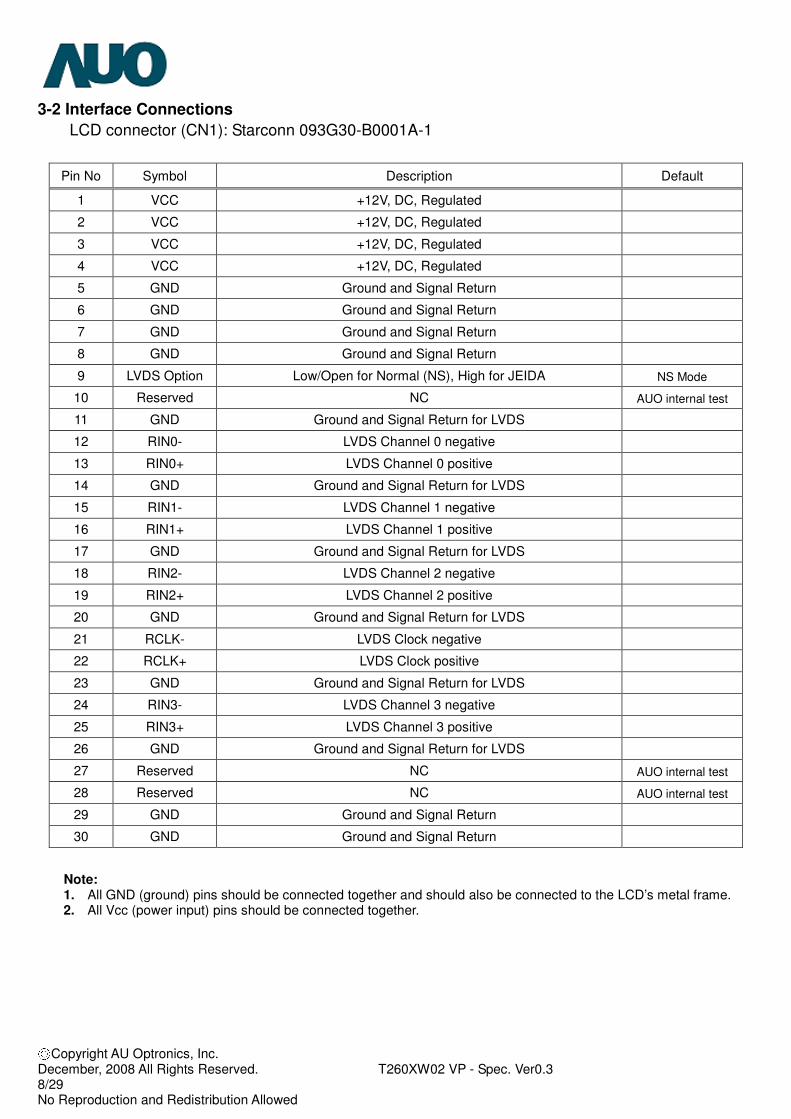
3-2 Interface Connections
LCD connector (CN1): Starconn 093G30-B0001A-1
Note: 1. All GND (ground) pins should be connected together and should also be connected to the LCD’s metal frame. 2. All Vcc (power input) pins should be connected together.
Pin No Symbol Description Default
1 VCC +12V, DC, Regulated
2 VCC +12V, DC, Regulated
3 VCC +12V, DC, Regulated
4 VCC +12V, DC, Regulated
5 GND Ground and Signal Return
6 GND Ground and Signal Return
7 GND Ground and Signal Return
8 GND Ground and Signal Return
9 LVDS Option Low/Open for Normal (NS), High for JEIDA NS Mode
10 Reserved NC AUO internal test
11 GND Ground and Signal Return for LVDS
12 RIN0- LVDS Channel 0 negative
13 RIN0+ LVDS Channel 0 positive
14 GND Ground and Signal Return for LVDS
15 RIN1- LVDS Channel 1 negative
16 RIN1+ LVDS Channel 1 positive
17 GND Ground and Signal Return for LVDS
18 RIN2- LVDS Channel 2 negative
19 RIN2+ LVDS Channel 2 positive
20 GND Ground and Signal Return for LVDS
21 RCLK- LVDS Clock negative
22 RCLK+ LVDS Clock positive
23 GND Ground and Signal Return for LVDS
24 RIN3- LVDS Channel 3 negative
25 RIN3+ LVDS Channel 3 positive
26 GND Ground and Signal Return for LVDS
27 Reserved NC AUO internal test
28 Reserved NC AUO internal test
29 GND Ground and Signal Return
30 GND Ground and Signal Return
Copyright AU Optronics, Inc. December, 2008 All Rights Reserved. T260XW02 VP - Spec. Ver0.3 9/29 No Reproduction and Redistribution Allowed
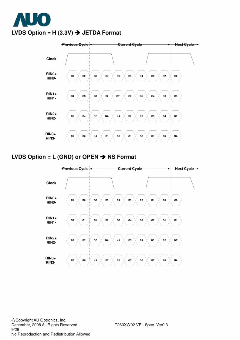
LVDS Option = H (3.3V) JETDA Format
B4NA DEDEB4B5 B6B7NA B5
R2R7 G2G2R2R3 R4R5R6 R3
G3B2 B3B3G3G4 G5G6 G4
Previous Cycle Current Cycle Next Cycle
Clock
RIN0+RIN0-
RIN1+RIN1-
RIN2+RIN2-
R0B1 NANAR0R1 G0G1B0 R1RIN3+RIN3-
G7
LVDS Option = L (GND) or OPEN NS Format
B2NA DEDEB2B3 B4B5NA
R0R5 G0G0R0R1 R2R3R4 R1
G1B0 B1B1G1G2 G3G4G5 G2
Previous Cycle Current Cycle Next Cycle
Clock
RIN0+RIN0-
RIN1+RIN1-
RIN2+RIN2-
R6B7 NANAR6R7 G6G7B6 R7RIN3+RIN3-
B3
Copyright AU Optronics, Inc. December, 2008 All Rights Reserved. T260XW02 VP - Spec. Ver0.3 10/29 No Reproduction and Redistribution Allowed
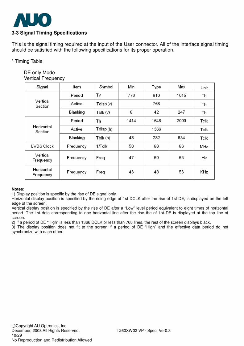
3-3 Signal Timing Specifications This is the signal timing required at the input of the User connector. All of the interface signal timing should be satisfied with the following specifications for its proper operation. * Timing Table
DE only Mode Vertical Frequency
Notes: 1) Display position is specific by the rise of DE signal only. Horizontal display position is specified by the rising edge of 1st DCLK after the rise of 1st DE, is displayed on the left edge of the screen. Vertical display position is specified by the rise of DE after a “Low” level period equivalent to eight times of horizontal period. The 1st data corresponding to one horizontal line after the rise the of 1st DE is displayed at the top line of screen. 2) If a period of DE “High” is less than 1366 DCLK or less than 768 lines, the rest of the screen displays black. 3) The display position does not fit to the screen if a period of DE “High” and the effective data period do not synchronize with each other.
Copyright AU Optronics, Inc. December, 2008 All Rights Reserved. T260XW02 VP - Spec. Ver0.3 11/29 No Reproduction and Redistribution Allowed
3-4 Signal Timing Waveforms
Th
Tdisp(v)
Tv
DE
RG
BD
ata768Line
Invalid Data
Invalid Data
1Line
2Line
3Line
768Line
4Line
Tclk
CLK
DE
RG
B D
ataPixel
1366Invalid D
ataP
ixel1
Pixel2
Pixel3
Pixel4
Pixel5
Pixel6
Pixel
1366Invalid D
ataPixel1
Pixel2
Th
Tdisp(h)
Copyright AU Optronics, Inc. December, 2008 All Rights Reserved. T260XW02 VP - Spec. Ver0.3 12/29 No Reproduction and Redistribution Allowed
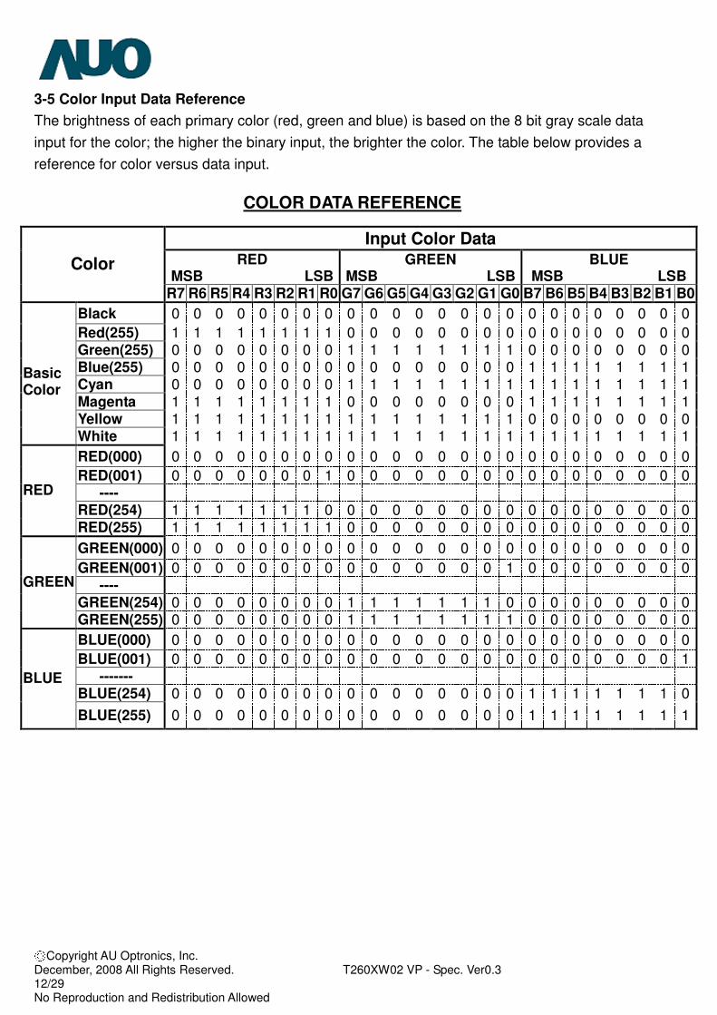
3-5 Color Input Data Reference
The brightness of each primary color (red, green and blue) is based on the 8 bit gray scale data
input for the color; the higher the binary input, the brighter the color. The table below provides a
reference for color versus data input.
COLOR DATA REFERENCE
Input Color Data RED
MSB LSB GREEN
MSB LSB BLUE
MSB LSB Color
R7 R6 R5 R4 R3 R2 R1 R0 G7 G6 G5 G4 G3 G2 G1 G0 B7 B6 B5 B4 B3 B2 B1 B0
Black 0 0 0 0 0 0 0 0 0 0 0 0 0 0 0 0 0 0 0 0 0 0 0 0
Red(255) 1 1 1 1 1 1 1 1 0 0 0 0 0 0 0 0 0 0 0 0 0 0 0 0 Green(255) 0 0 0 0 0 0 0 0 1 1 1 1 1 1 1 1 0 0 0 0 0 0 0 0 Blue(255) 0 0 0 0 0 0 0 0 0 0 0 0 0 0 0 0 1 1 1 1 1 1 1 1 Cyan 0 0 0 0 0 0 0 0 1 1 1 1 1 1 1 1 1 1 1 1 1 1 1 1 Magenta 1 1 1 1 1 1 1 1 0 0 0 0 0 0 0 0 1 1 1 1 1 1 1 1 Yellow 1 1 1 1 1 1 1 1 1 1 1 1 1 1 1 1 0 0 0 0 0 0 0 0
Basic Color
White 1 1 1 1 1 1 1 1 1 1 1 1 1 1 1 1 1 1 1 1 1 1 1 1
RED(000) 0 0 0 0 0 0 0 0 0 0 0 0 0 0 0 0 0 0 0 0 0 0 0 0
RED(001) 0 0 0 0 0 0 0 1 0 0 0 0 0 0 0 0 0 0 0 0 0 0 0 0 ---- RED(254) 1 1 1 1 1 1 1 0 0 0 0 0 0 0 0 0 0 0 0 0 0 0 0 0
RED
RED(255) 1 1 1 1 1 1 1 1 0 0 0 0 0 0 0 0 0 0 0 0 0 0 0 0
GREEN(000) 0 0 0 0 0 0 0 0 0 0 0 0 0 0 0 0 0 0 0 0 0 0 0 0
GREEN(001) 0 0 0 0 0 0 0 0 0 0 0 0 0 0 0 1 0 0 0 0 0 0 0 0 ---- GREEN(254) 0 0 0 0 0 0 0 0 1 1 1 1 1 1 1 0 0 0 0 0 0 0 0 0
GREEN
GREEN(255) 0 0 0 0 0 0 0 0 1 1 1 1 1 1 1 1 0 0 0 0 0 0 0 0
BLUE(000) 0 0 0 0 0 0 0 0 0 0 0 0 0 0 0 0 0 0 0 0 0 0 0 0
BLUE(001) 0 0 0 0 0 0 0 0 0 0 0 0 0 0 0 0 0 0 0 0 0 0 0 1 ------- BLUE(254) 0 0 0 0 0 0 0 0 0 0 0 0 0 0 0 0 1 1 1 1 1 1 1 0
BLUE
BLUE(255) 0 0 0 0 0 0 0 0 0 0 0 0 0 0 0 0 1 1 1 1 1 1 1 1
Copyright AU Optronics, Inc. December, 2008 All Rights Reserved. T260XW02 VP - Spec. Ver0.3 13/29 No Reproduction and Redistribution Allowed
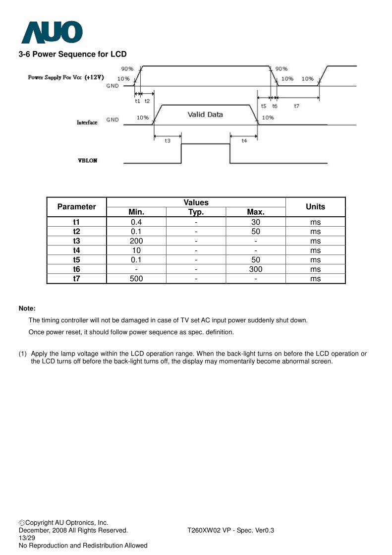
3-6 Power Sequence for LCD
Values Parameter
Min. Typ. Max. Units
t1 0.4 - 30 ms t2 0.1 - 50 ms t3 200 - - ms t4 10 - - ms t5 0.1 - 50 ms t6 - - 300 ms t7 500 - - ms
Note:
The timing controller will not be damaged in case of TV set AC input power suddenly shut down.
Once power reset, it should follow power sequence as spec. definition.
(1) Apply the lamp voltage within the LCD operation range. When the back-light turns on before the LCD operation or the LCD turns off before the back-light turns off, the display may momentarily become abnormal screen.
Copyright AU Optronics, Inc. December, 2008 All Rights Reserved. T260XW02 VP - Spec. Ver0.3 14/29 No Reproduction and Redistribution Allowed
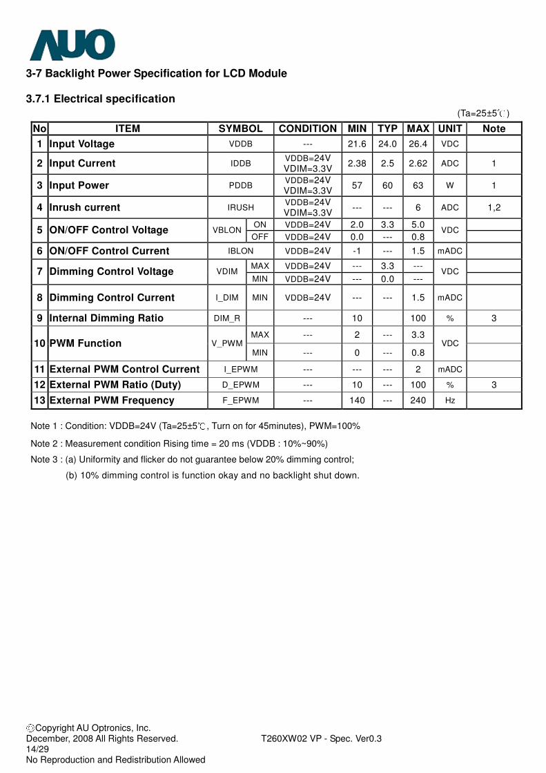
3-7 Backlight Power Specification for LCD Module 3.7.1 Electrical specification (Ta=25±5 )
No ITEM SYMBOL CONDITION MIN TYP MAX UNIT Note
1 Input Voltage VDDB --- 21.6 24.0 26.4 VDC
2 Input Current IDDB VDDB=24V VDIM=3.3V
2.38 2.5 2.62 ADC 1
3 Input Power PDDB VDDB=24V VDIM=3.3V
57 60 63 W 1
4 Inrush current IRUSH VDDB=24V VDIM=3.3V
--- --- 6 ADC 1,2
ON VDDB=24V 2.0 3.3 5.0 5 ON/OFF Control Voltage VBLON
OFF VDDB=24V 0.0 --- 0.8 VDC
6 ON/OFF Control Current IBLON VDDB=24V -1 --- 1.5 mADC
MAX VDDB=24V --- 3.3 --- 7 Dimming Control Voltage VDIM
MIN VDDB=24V --- 0.0 --- VDC
8 Dimming Control Current I_DIM MIN VDDB=24V --- --- 1.5 mADC
9 Internal Dimming Ratio DIM_R --- 10 100 % 3
MAX --- 2 --- 3.3 10 PWM Function V_PWM
MIN --- 0 --- 0.8 VDC
11 External PWM Control Current I_EPWM --- --- --- 2 mADC
12 External PWM Ratio (Duty) D_EPWM --- 10 --- 100 % 3
13 External PWM Frequency F_EPWM --- 140 --- 240 Hz
Note 1 : Condition: VDDB=24V (Ta=25±5 , Turn on for 45minutes), PWM=100%
Note 2 : Measurement condition Rising time = 20 ms (VDDB : 10%~90%)
Note 3 : (a) Uniformity and flicker do not guarantee below 20% dimming control;
(b) 10% dimming control is function okay and no backlight shut down.
Copyright AU Optronics, Inc. December, 2008 All Rights Reserved. T260XW02 VP - Spec. Ver0.3 15/29 No Reproduction and Redistribution Allowed
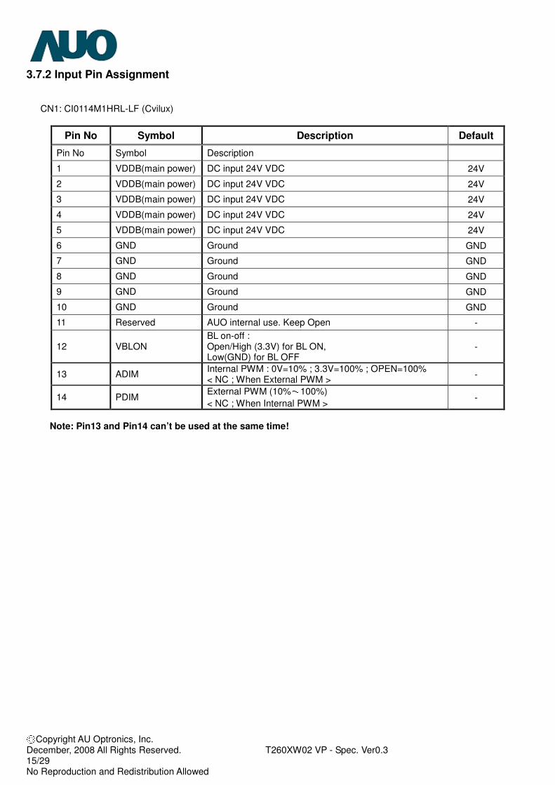
3.7.2 Input Pin Assignment
CN1: CI0114M1HRL-LF (Cvilux)
Note: Pin13 and Pin14 can’t be used at the same time!
Pin No Symbol Description Default
Pin No Symbol Description
1 VDDB(main power) DC input 24V VDC 24V
2 VDDB(main power) DC input 24V VDC 24V
3 VDDB(main power) DC input 24V VDC 24V
4 VDDB(main power) DC input 24V VDC 24V
5 VDDB(main power) DC input 24V VDC 24V
6 GND Ground GND
7 GND Ground GND
8 GND Ground GND
9 GND Ground GND
10 GND Ground GND
11 Reserved AUO internal use. Keep Open -
12 VBLON BL on-off : Open/High (3.3V) for BL ON, Low(GND) for BL OFF
-
13 ADIM Internal PWM : 0V=10% ; 3.3V=100% ; OPEN=100% < NC ; When External PWM >
-
14 PDIM External PWM (10% 100%)
< NC ; When Internal PWM > -
Copyright AU Optronics, Inc. December, 2008 All Rights Reserved. T260XW02 VP - Spec. Ver0.3 16/29 No Reproduction and Redistribution Allowed
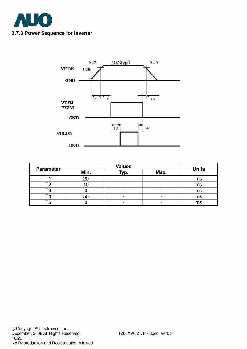
3.7.3 Power Sequence for Inverter
Values Parameter
Min. Typ. Max. Units
T1 20 - - ms T2 10 - - ms T3 0 - - ms T4 50 - - ms T5 0 - - ms
Copyright AU Optronics, Inc. December, 2008 All Rights Reserved. T260XW02 VP - Spec. Ver0.3 17/29 No Reproduction and Redistribution Allowed
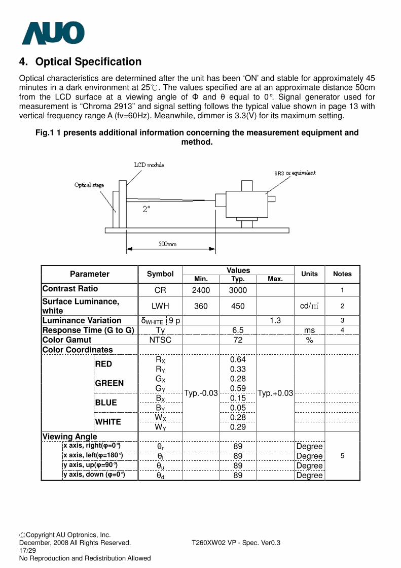
4. Optical Specification
Optical characteristics are determined after the unit has been ‘ON’ and stable for approximately 45 minutes in a dark environment at 25!. The values specified are at an approximate distance 50cm from the LCD surface at a viewing angle of Φ and θ equal to 0°. Signal generator used for measurement is “Chroma 2913” and signal setting follows the typical value shown in page 13 with vertical frequency range A (fv=60Hz). Meanwhile, dimmer is 3.3(V) for its maximum setting.
Fig.1 1 presents additional information concerning the measurement equipment and method.
Values Parameter Symbol Min. Typ. Max.
Units Notes
Contrast Ratio CR 2400 3000 1
Surface Luminance, white
LWH 360 450 cd/! 2
Luminance Variation δWHITE 9 p 1.3 3
Response Time (G to G) Tγ 6.5 ms 4
Color Gamut NTSC 72 %
Color Coordinates
RX 0.64 RED
RY 0.33
GX 0.28 GREEN
GY 0.59
BX 0.15 BLUE
BY 0.05
WX 0.28
WHITE WY
Typ.-0.03
0.29
Typ.+0.03
Viewing Angle x axis, right(φ=0°) θr 89 Degree x axis, left(φ=180°) θl 89 Degree y axis, up(φ=90°) θu 89 Degree
y axis, down (φ=0°) θd 89 Degree
5
Copyright AU Optronics, Inc. December, 2008 All Rights Reserved. T260XW02 VP - Spec. Ver0.3 18/29 No Reproduction and Redistribution Allowed
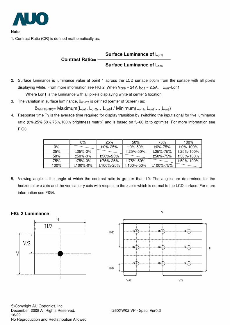
Note:
1. Contrast Ratio (CR) is defined mathematically as:
Surface Luminance of Lon5 Contrast Ratio=
Surface Luminance of Loff5
2. Surface luminance is luminance value at point 1 across the LCD surface 50cm from the surface with all pixels
displaying white. From more information see FIG 2. When VDDB = 24V, IDDB = 2.5A. LWH=Lon1
Where Lon1 is the luminance with all pixels displaying white at center 5 location.
3. The variation in surface luminance, δWHITE is defined (center of Screen) as:
δWHITE(9P)= Maximum(Lon1, Lon2,…Lon9) / Minimum(Lon1, Lon2,…,Lon9)
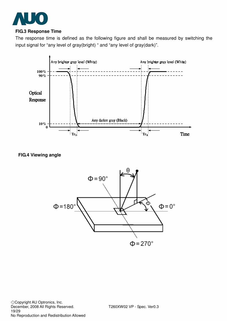
4. Response time Tγ is the average time required for display transition by switching the input signal for five luminance
ratio (0%,25%,50%,75%,100% brightness matrix) and is based on fv=60Hz to optimize. For more information see
FIG3.
0% 25% 50% 75% 100% 0% t:0%-25% t:0%-50% t:0%-75% t:0%-100% 25% t:25%-0% t:25%-50% t:25%-75% t:25%-100% 50% t:50%-0% t:50%-25% t:50%-75% t:50%-100% 75% t:75%-0% t:75%-25% t:75%-50% t:50%-100% 100% t:100%-0% t:100%-25% t:100%-50% t:100%-75%
5. Viewing angle is the angle at which the contrast ratio is greater than 10. The angles are determined for the
horizontal or x axis and the vertical or y axis with respect to the z axis which is normal to the LCD surface. For more
information see FIG4.
FIG. 2 Luminance
1 2 3
4 5 6
7 8 9
H
V
H/6
H/2
V/2 V/6
Copyright AU Optronics, Inc. December, 2008 All Rights Reserved. T260XW02 VP - Spec. Ver0.3 19/29 No Reproduction and Redistribution Allowed
FIG.3 Response Time
The response time is defined as the following figure and shall be measured by switching the
input signal for “any level of gray(bright) “ and “any level of gray(dark)”.
FIG.4 Viewing angle
TrD
!!!! """"!!!! ####$$$$
!"#$!"#$!"#$!"#$ TrR
10%
%&'"()*+%&'"()*+%&'"()*+%&'"()*+
,$-&./-$,$-&./-$,$-&./-$,$-&./-$
100%
90%
0
Copyright AU Optronics, Inc. December, 2008 All Rights Reserved. T260XW02 VP - Spec. Ver0.3 20/29 No Reproduction and Redistribution Allowed
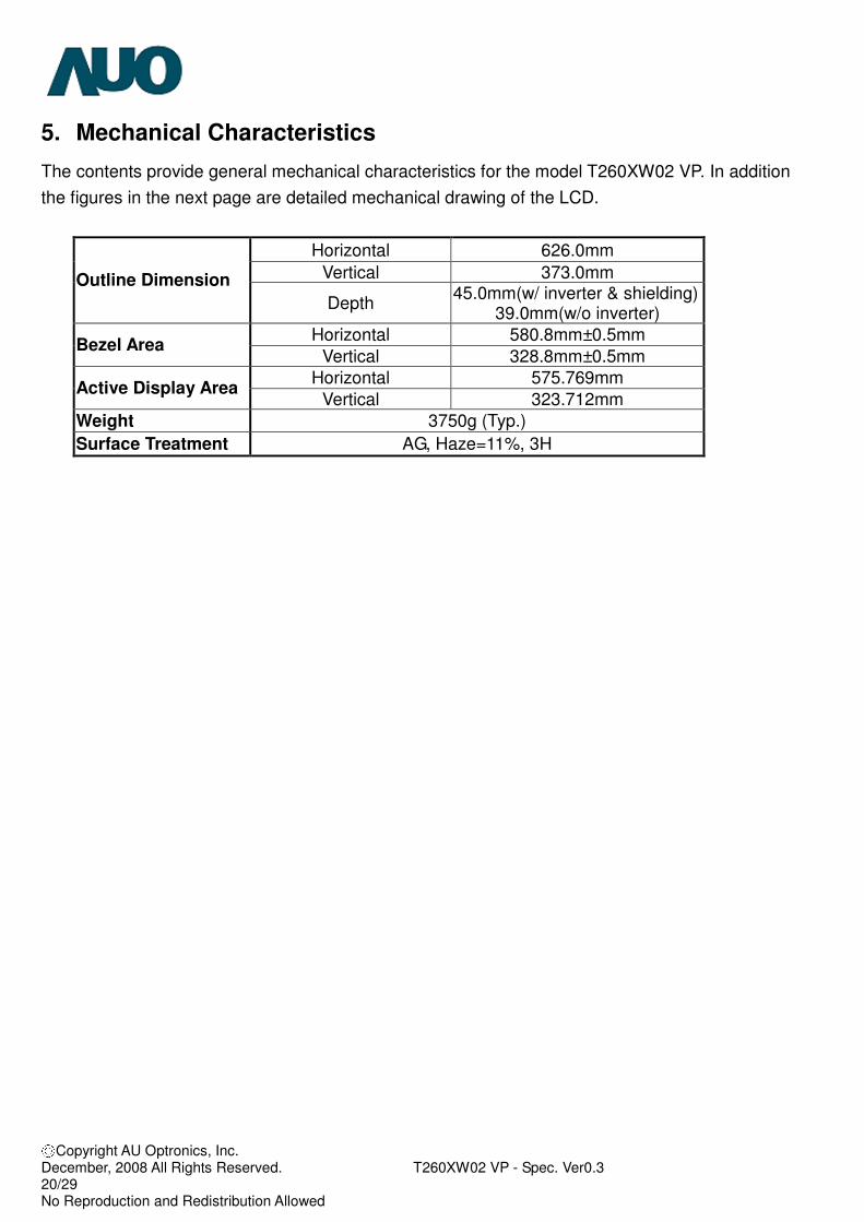
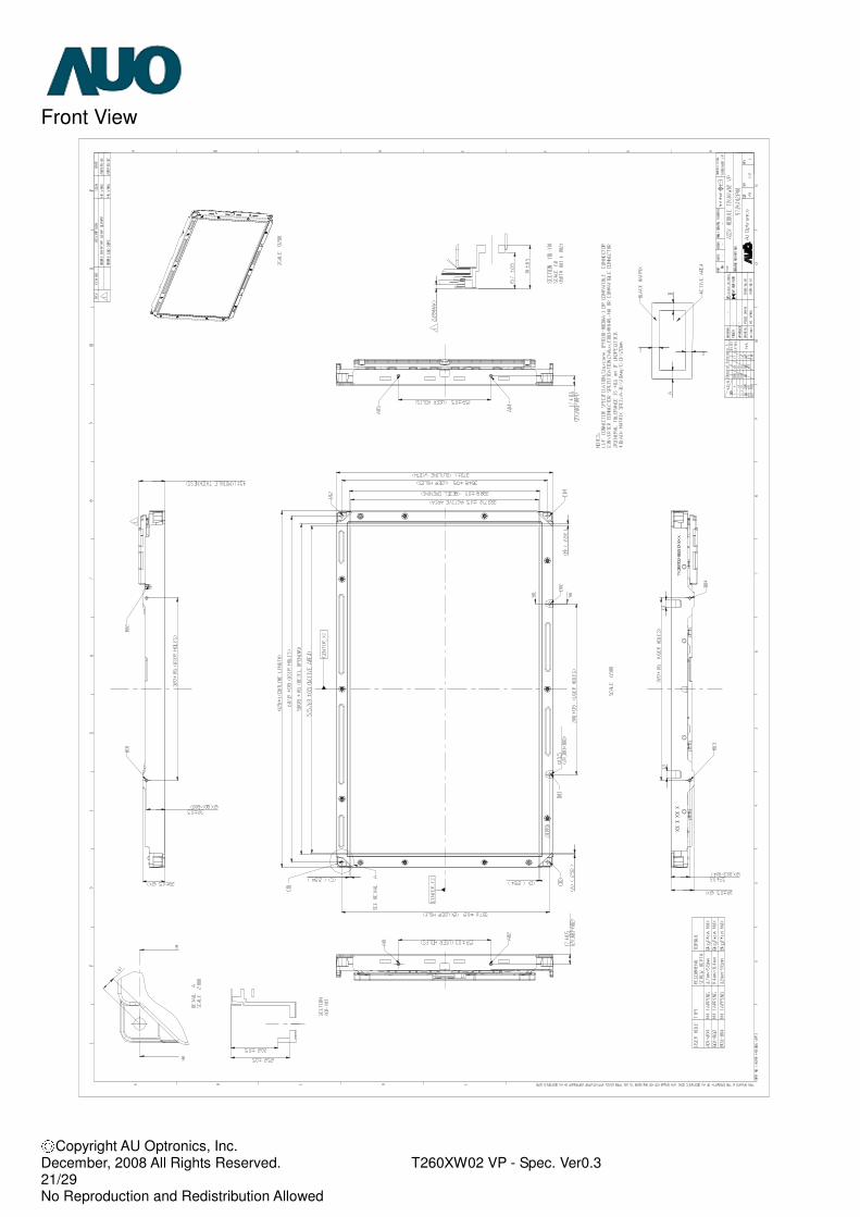
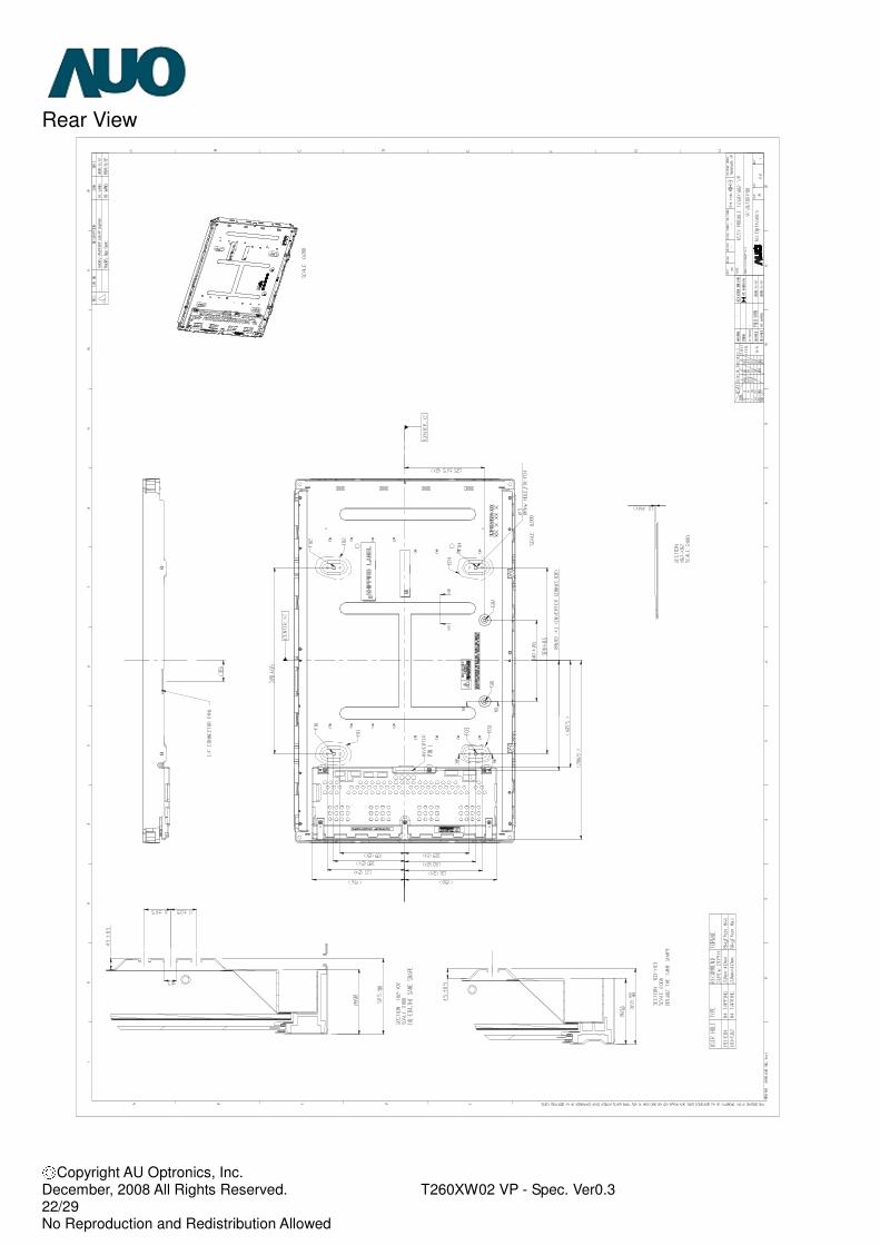
5. Mechanical Characteristics
The contents provide general mechanical characteristics for the model T260XW02 VP. In addition
the figures in the next page are detailed mechanical drawing of the LCD.
Horizontal 626.0mm Vertical 373.0mm Outline Dimension
Depth 45.0mm(w/ inverter & shielding)
39.0mm(w/o inverter) Horizontal 580.8mm±0.5mm
Bezel Area Vertical 328.8mm±0.5mm
Horizontal 575.769mm Active Display Area
Vertical 323.712mm Weight 3750g (Typ.)
Surface Treatment AG, Haze=11%, 3H
Copyright AU Optronics, Inc. December, 2008 All Rights Reserved. T260XW02 VP - Spec. Ver0.3 21/29 No Reproduction and Redistribution Allowed
Front View
Copyright AU Optronics, Inc. December, 2008 All Rights Reserved. T260XW02 VP - Spec. Ver0.3 22/29 No Reproduction and Redistribution Allowed
Rear View
Copyright AU Optronics, Inc. December, 2008 All Rights Reserved. T260XW02 VP - Spec. Ver0.3 23/29 No Reproduction and Redistribution Allowed
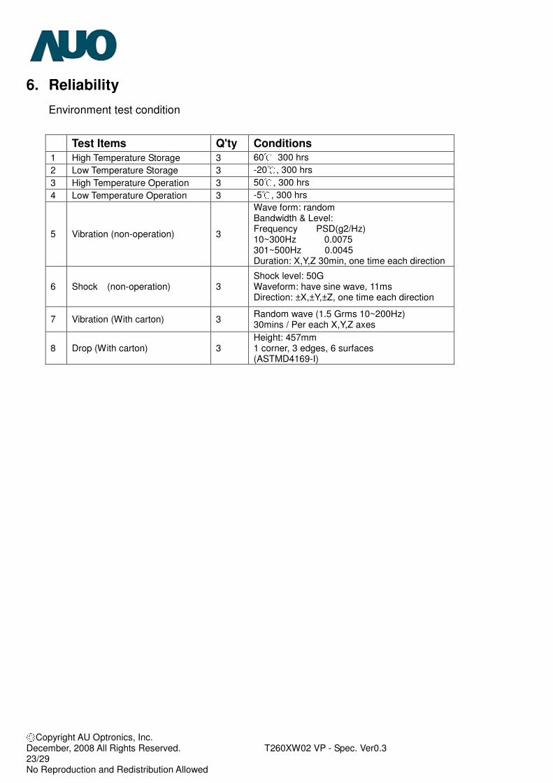
6. Reliability
Environment test condition
Test Items Q'ty Conditions 1 High Temperature Storage 3 60 300 hrs
2 Low Temperature Storage 3 -20 , 300 hrs
3 High Temperature Operation 3 50 , 300 hrs
4 Low Temperature Operation 3 -5 , 300 hrs
5 Vibration (non-operation) 3
Wave form: random Bandwidth & Level: Frequency PSD(g2/Hz) 10~300Hz 0.0075 301~500Hz 0.0045 Duration: X,Y,Z 30min, one time each direction
6 Shock (non-operation) 3 Shock level: 50G Waveform: have sine wave, 11ms Direction: ±X,±Y,±Z, one time each direction
7 Vibration (With carton) 3 Random wave (1.5 Grms 10~200Hz) 30mins / Per each X,Y,Z axes
8 Drop (With carton) 3 Height: 457mm 1 corner, 3 edges, 6 surfaces (ASTMD4169-I)
Copyright AU Optronics, Inc. December, 2008 All Rights Reserved. T260XW02 VP - Spec. Ver0.3 24/29 No Reproduction and Redistribution Allowed
7. International Standard
7-1 Safety
(1) UL1950 Third Edition, Underwriters Laboratories, Inc. Jan. 28, 1995
Standard for Safety of Information Technology Equipment Including electrical Business
Equipment.
(2) CAN/CSA C22.2 No. 950-95 Third Edition, Canadian Standards Association, Jan. 28, 1995
Standard for Safety of Information Technology Equipment Including Electrical Business
Equipment.
(3) EN60950: 1992+A2: 1993+A2: 1993+C3: 1995+A4: 1997+A11: 1997
IEC 950: 1991+A1: 1992+A2: 1993+C3: 1995+A4:1996
European Committee for Electro technical Standardization (CENELEC)
EUROPEAN STANDARD for Safety of Information Technology Equipment Including Electrical
Business Equipment.
(4) EN 60065:2002; IEC 60065:2001
7-2 EMC
a) ANSI C63.4 “Methods of Measurement of Radio-Noise Emissions from Low-Voltage
Electrical and Electrical Equipment in the Range of 9kHz to 40GHz. “American National
standards Institute(ANSI), 1992.
b) C.I.S.P.R “Limits and Methods of Measurement of Radio Interface Characteristics of
Information Technology Equipment.” International Special committee on Radio Interference.
c) EN 55022 “Limits and Methods of Measurement of Radio Interface Characteristics of
Information Technology Equipment.” European Committee for Electro technical
Standardization. (CENELEC), 1998.
7-3 Green
Green Mark Description:
a) For Pb Free products, AUO will add for identification.
b) For RoHS compatible products, AUO will add for identification.
Note.
The Green Mark will be present only when the green documents have been ready by AUO Internal Green Team. (The
definition of green design follows the AUO green design checklist.)
Copyright AU Optronics, Inc. December, 2008 All Rights Reserved. T260XW02 VP - Spec. Ver0.3 25/29 No Reproduction and Redistribution Allowed
8. Packing
Label sample
838A0584AHZ – ZS0200
838A0584AHZZ: Panel Unique ID
ZS0200: AUO internal use
Manufactured 09/02
2009 week 02
AM89018
AUO internal use
Carton Label
Carton Size 722(L) mm*325(W) mm*469(H) mm
AU Optronics XXXXG Made in China (S1)
Manufactured 09/02 AM89018 Model NO: T260XW02 VP
*838A0584AHZZ – ZS0200*
CARTON NO:
CUSTOMER NO:
Made in Taiwan
MODEL NO: T260XW02 VX
*PM100-01A1600001*
QTY: 4
PART NO: 97.26T02.XXX
AU Optronics 5
Copyright AU Optronics, Inc. December, 2008 All Rights Reserved. T260XW02 VP - Spec. Ver0.3 26/29 No Reproduction and Redistribution Allowed
!"#$%&'()*+$%
,)$-.'/%$+0%
1"#$%&'()*+2345%678%
,)$-.'/%0'"%
&'()*+%
!"#$%2%1%#790'/!!!!
,)$-.'/%(':/%
Copyright AU Optronics, Inc. December, 2008 All Rights Reserved. T260XW02 VP - Spec. Ver0.3 27/29 No Reproduction and Redistribution Allowed
Pallet and Shipment information
Specification Item
Qty. Dimension Weight (kg) Packing Remark
1 Packing BOX 5pcs/box 722(L)mm*325(W)mm*469(H)mm 25
2 Pallet 1 980(L)mm*740(W)mm*138(H)mm 13
3 Boxes per Pallet 6 boxes/pallet
4 Panels per Pallet 30pcs/pallet
Pallet after packing 30 980(L)mm*740(W)mm*1076(H)mm
163
Label
Pallet
PET band
Corner protector
Copyright AU Optronics, Inc. December, 2008 All Rights Reserved. T260XW02 VP - Spec. Ver0.3 28/29 No Reproduction and Redistribution Allowed
9. PRECAUTIONS
Please pay attention to the followings when you use this TFT LCD module.
9-1 MOUNTING PRECAUTIONS
(1) You must mount a module using holes arranged in four corners or four sides. (2) You should consider the mounting structure so that uneven force (ex. Twisted stress) is not applied to module. And the case on which a module is mounted should have sufficient strength so that external force is not transmitted directly to the module. (3) Please attach the surface transparent protective plate to the surface in order to protect the polarizer. Transparent protective plate should have sufficient strength in order to the resist external force. (4) You should adopt radiation structure to satisfy the temperature specification. (5) Acetic acid type and chlorine type materials for the cover case are not desirable because the former generates corrosive gas of attacking the polarizer at high temperature and the latter causes circuit break by electro-chemical reaction. (6) Do not touch, push or rub the exposed polarizers with glass, tweezers or anything harder than HB pencil lead. And please do not rub with dust clothes with chemical treatment. Do not touch the surface of polarizer for bare hand or greasy cloth. (Some cosmetics are detrimental to the polarizer.) (7) When the surface becomes dusty, please wipe gently with absorbent cotton or other soft materials like chamois soaks with petroleum benzene. Normal-hexane is recommended for cleaning the adhesives used to attach front/ rear polarizers. Do not use acetone, toluene and alcohol because they cause chemical damage to the polarizer. (8) Wipe off saliva or water drops as soon as possible. Their long time contact with polarizer causes deformations and color fading. (9) Do not open the case because inside circuits do not have sufficient strength.
9-2 OPERATING PRECAUTIONS
(1) The device listed in the product specification sheets was designed and manufactured for
TV application
(2) The spike noise causes the mis-operation of circuits. It should be lower than following
voltage: V=±200mV(Over and under shoot voltage)
(3) Response time depends on the temperature. (In lower temperature, it becomes longer.)
(4) Brightness depends on the temperature. (In lower temperature, it becomes lower.) And in
lower temperature, response time (required time that brightness is stable after turned on)
becomes longer.
(5) Be careful for condensation at sudden temperature change. Condensation makes damage
to polarizer or electrical contacted parts. And after fading condensation, smear or spot will
occur.
(6) When fixed patterns are displayed for a long time, remnant image is likely to occur.
(7) Module has high frequency circuits. Sufficient suppression to the electromagnetic
interference shall be done by system manufacturers. Grounding and shielding methods may
Copyright AU Optronics, Inc. December, 2008 All Rights Reserved. T260XW02 VP - Spec. Ver0.3 29/29 No Reproduction and Redistribution Allowed
be important to minimize the interface.
9-3 ELECTROSTATIC DISCHARGE CONTROL
Since a module is composed of electronic circuits, it is not strong to electrostatic discharge. Make
certain that treatment persons are connected to ground through wrist band etc. And don’t touch
interface pin directly.
9-4 PRECAUTIONS FOR STRONG LIGHT EXPOSURE
Strong light exposure causes degradation of polarizer and color filter.
9-5 STORAGE
When storing modules as spares for a long time, the following precautions are necessary.
(1) Store them in a dark place. Do not expose the module to sunlight or fluorescent light.
Keep the temperature between 5! and 35! at normal humidity.
(2) The polarizer surface should not come in contact with any other object. It is recommended
that they be stored in the container in which they were shipped.
9-6 HANDLING PRECAUTIONS FOR PROTECTION FILM
(1) The protection film is attached to the bezel with a small masking tape. When the protection
film is peeled off, static electricity is generated between the film and polarizer. This should be
peeled off slowly and carefully by people who are electrically grounded and with well
ion-blown equipment or in such a condition, etc.
(2) When the module with protection film attached is stored for a long time, sometimes there
remains a very small amount of flue still on the Bezel after the protection film is peeled off.
(3) You can remove the glue easily. When the glue remains on the Bezel or its vestige is
recognized, please wipe them off with absorbent cotton waste or other soft material like
chamois soaked with normal-hexane.