cx plus - modbus · technical documentation cx plus modbus rev. 02 2018-07 6 1.2 safety notes and...
TRANSCRIPT
Technical Documentation CX plus Modbus
Rev. 02
2018-07
Beluk GmbH Taubenstrasse 1 86956 Schongau Germany
Tel.: +49/(0)8861/2332-0 Fax: +49/(0)8861/2332-22 E-Mail: [email protected] Web: http://www.beluk.de
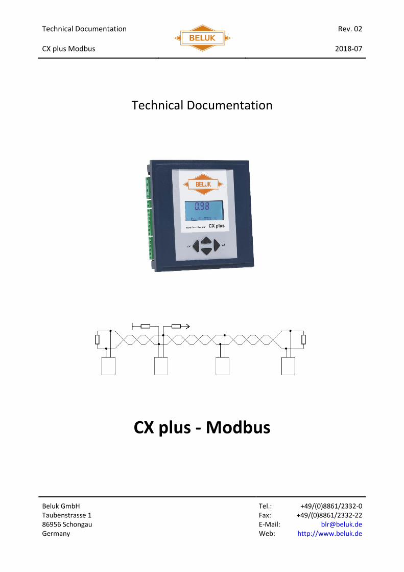
Technical Documentation
CX plus - Modbus

Technical Documentation CX plus Modbus
Rev. 02
2018-07
2
Revision list
Date Name Revision Comment
25.09.17 ChP 01 First edition
04.07.18 SO 02 Adaption to Firmware 1.1

Technical Documentation CX plus Modbus
Rev. 02
2018-07
3
Table of contents
1 SAFETY NOTES ........................................................................................................................... 5
1.1 Symbols................................................................................................................................................ 5
1.2 Safety notes and further information ........................................................................................... 6
2 OVERVIEW ................................................................................................................................... 7
3 MODBUS/RS485 .......................................................................................................................... 7
3.1 Physical level - RS485 (defined in EIA485/ISO8482) ................................................................ 8
3.1.1 2-wire and 4-wire bus ................................................................................................................... 8
3.1.2 3-pole plug connection ................................................................................................................. 9
3.1.3 Wire termination ............................................................................................................................ 9
3.1.4 Bias voltage (line biasing) ........................................................................................................... 9
3.1.5 Communication indicator ........................................................................................................... 10
3.2 The Modbus protocol ...................................................................................................................... 11
3.2.1 Modbus description .................................................................................................................... 11
3.2.2 Serial data format and data frame............................................................................................ 11
3.2.3 Serial transmission types ........................................................................................................... 12
3.2.4 Function codes ............................................................................................................................ 12
3.2.5 Exception codes .......................................................................................................................... 13
3.2.6 Master-slave protocol ................................................................................................................. 14
3.2.7 Address space............................................................................................................................. 14
3.2.8 Modbus addressing .................................................................................................................... 15
4 MODBUS SETTINGS OF THE REACTIVE POWER CONTROLLER CX PLUS ..................... 16
4.1 Reactive power controller CX plus - Modbus setup ............................................................... 16
4.2 Important RS485 BUS connection parameters ........................................................................ 16
5 ADDRESSES AND REGISTERS ............................................................................................... 17
5.1 Measurement values ....................................................................................................................... 17
5.1.1 Modbus addresses of the measurement values .................................................................... 17
5.1.2 Modbus addresses of the measurement values (continuation) ........................................... 18
5.2 Device settings (USER PARAMETERS) ..................................................................................... 19
5.2.1 User parameter flags 1 .............................................................................................................. 21
5.3 Stage database ................................................................................................................................. 23
5.3.1 Stage type settings ..................................................................................................................... 23
5.3.2 Bits stage type settings 6-stage controller .............................................................................. 25
5.3.3 Bits stage type settings 12-stage controller ............................................................................ 26
5.3.4 Manual switching of stages via MODBUS .............................................................................. 26
5.3.5 Stage data .................................................................................................................................... 27
5.3.6 Stage date of the 6-stage controller ......................................................................................... 28

Technical Documentation CX plus Modbus
Rev. 02
2018-07
4
5.3.7 Stage data of the 6-stage controller (continuation) ............................................................... 29
5.3.8 Stage data of the 12-stage controller ...................................................................................... 30
5.3.9 Stage data of the 12-stage controller (continuation) ............................................................. 31
5.4 States of the switching outputs ................................................................................................... 32
5.4.1 States of the switching outputs of the 6-stage controller ...................................................... 32
5.4.2 States of the switching outputs of the 12-stage controller .................................................... 33
5.5 Extended operating hour counter of the stages in seconds ................................................ 34
5.5.1 Stage running time 12-stage controller ................................................................................... 35
5.6 Alarm status ...................................................................................................................................... 36
Alarm memory ............................................................................................................................................. 37
5.7 Device identification ....................................................................................................................... 39
5.8 Permanent storage of the device settings ................................................................................ 40
6 TROUBLESHOOTING ................................................................................................................ 41
7 ANNEX – ASCII TABLE ............................................................................................................. 45
8 NOTES ........................................................................................................................................ 46

Technical Documentation CX plus Modbus
Rev. 02
2018-07
5
1 Safety notes
Read these safety notes and instructions attentively and carefully first. Familiarise yourself with the device prior to installation, commissioning and operation! The following symbols are used in the manual and on the device label on the back of the device in order to indicate dangers and problems or to give specific instructions.
1.1 Symbols
! DANGER
DANGER indicates a dangerous situation which, if not avoided, may cause death or sever injuries.
! WARNING
WARNING indicates a dangerous situation which, if not avoided, may cause death or severe injuries.
! CAUTION
CAUTION indicates circumstances which may damage or destroy the device in case of non-observance, but do not cause injuries.
☝NOTE The note symbol indicates further information in order to describe special technical features in a more detailed way.

Technical Documentation CX plus Modbus
Rev. 02
2018-07
6
1.2 Safety notes and further information
! DANGER
During the installation of the reactive power controller CX plus, there is a risk of electric shock. For this reason, installation, commissioning and maintenance may exclusively be performed by a skilled electrician with the necessary qualification. A skilled electrician is a person who has the ability, experience and knowledge necessary for the construction, installation and operation of electrical equipment and systems and who is trained in the detection and prevention of potential hazards.
During installation, the relevant regulations for the installation of switchgear and for the prevention of accidents must be observed and complied with. Devices with damaged or open housing or open terminals may not be connected to the mains and must be disconnected immediately.
The current transformer must be short-circuited prior to disconnecting the current measurement path at the device resp. at the current transformer. Otherwise there may be a life-threatening voltage level at the connections of the current measurement path resp. of the transformer. In the long run, the transformer will be destroyed by the high voltage.
! WARNING
Before you change the parameter settings at the device, read this reference manual of the reactive power controller CX plus attentively and carefully in order to familiarise yourself with the individual device settings and the associated impacts.
! WARNING
Never change device settings via Modbus, if you do not know the consequences of the change beforehand or if someone is currently working at the system!
! WARNING
Never manually switch on or off compensation stages via Modbus, if you are not sure, what the switching operation will cause or if someone is currently working at the system!
! WARNING
Please observe, that the changes are immediately effective in the device after the writing process of the value!
! WARNING
Do not try to write addresses (resp. registers) via Modbus, which are not defined in this manual or are explicitly identified for writing!

Technical Documentation CX plus Modbus
Rev. 02
2018-07
7
! WARNING
When writing values, always observe the permissible setting range! Never write non-defined bits in bitmasks with a Boolean "1"!
! CAUTION
Modifications at the device settings made via Modbus are only saved in the “volatile memory” (RAM). All modifications at the device settings made via Modbus will be lost after a device restart (Reset)!
In order to prevent this, the device settings must be saved in the “non-volatile memory (FLASH)”.
The saving in the “non-volatile memory (FLASH)” must be activated explicitly. Information about this may be found in Paragraph 5.9 (Permanent storage of the device settings).
! CAUTION
Unnecessary writing activities in the FLASH memory will reduce its service life and thus the service life of the reactive power controller CX plus!
Consequently, frequent writing activities in the FLASH memory shall be avoided. Therefore, do not save the device settings in the “non-volatile memory (FLASH)” until you have made all settings!
2 Overview
The Modbus communication interface of the reactive power controller CX plus offers the possibility to read measurement values via a bus connection from remote computer systems in order to use these for further processing.
The present manual describes the data transmission using the Modbus protocol, which defines methods of data transport and addressing, but is not generally determined for a specific transmission medium (physical transmission level).
The reactive power controller CX plus uses the industrial standard RS485 for data transmission. This bus system additionally offers the possibility to operate several devices via the same BUS cable.
A multitude of commercial devices and programmable logic controllers (PLC) are compatible with the Modbus protocol as communication medium, which enables the user to realise a bus system with little effort.
3 MODBUS/RS485
The communication protocol Modbus RTU basically consists of two levels:
The industrial standard RS485 is used as underlying data transmission medium. This controls the physical transmission of the data byte between the bus participants and is recognised by high-quality levels, the Modbus application protocol.
The Modbus application protocol uses the underlying RS485 protocol for data transmission. It defines commands (so-called “Function Codes”, FC), addresses and data structures.

Technical Documentation CX plus Modbus
Rev. 02
2018-07
8
☝NOTE Further information on the MODBUS protocol can be found at www.Modbus.org. The currently valid bus specifications are also available here.
3.1 Physical level - RS485 (defined in EIA485/ISO8482)
3.1.1 2-wire and 4-wire bus
The communication standard RS485 uses two wires for data transport D(+) and D(-). The two symmetrical data wires always work with a differential voltage level of at least ± 200 mV. This results in a total of two possibilities presented by the two logical levels “low” and “high”. Due to this differential transmission technology, the standard RS485 is particularly resistant to electromagnetic interferences and wire lengths of more than 1000 metres may be reached.
The reactive power controller CX plus is compatible with the following transmission rates (baud rates, see Paragraph 3.2.3): 1200; 2400; 4800; 19200; 38400; 57600 and 115200 baud. All parity variations (even, odd and none) are compatible.
Differences between the variations of the communication standards RS485:
2-wire RS485: This type uses two wires for the communication, so that the same wire pair must be used for both data directions. Therefore, it is necessary to switch between sending and reception process at each device (half-duplex mode).
4-wire RS485: In this case, a wire pair each is used for both data directions. Switching is only necessary for the senders of the slave devices. Due to the Modbus protocol, however, it is also only possible to use the half-duplex mode in this case. Thus, it is not possible to increase the transmission capacity.
☝NOTE The reactive power controller CX plus is exclusively compatible with the 2-wire mode!
Both types require another wire each, which must be connected between all bus devices: The common ground signal GND.
! CAUTION
The shield of the cable must not be connected for this purpose!
The cable shield shall be connected with the ground potential in order to reduce interferences from the outside.
The standard RS485 is compatible with several devices at one bus wire (usually up to 32 participants). For this purpose, all signals of the devices must be connected in parallel. Usually, this are the data wires D(+) and D(-) as well as the signal ground (GND or GROUND).
A bus wire with all connected participants is called a bus segment. The data may be exchanged between several segments by means of the so-called “repeaters”.

Technical Documentation CX plus Modbus
Rev. 02
2018-07
9
3.1.2 3-pole plug connection
Figure 1: Connector plug with symbolic marking of the Modbus communication interface of the reactive power controller CX plus
A 3-pole plug connector is provided for the connection of the Modbus interface. The symbolism in the adjacent figure illustrates the terminal assignment.
For commissioning, the data wires + with D(+) and - with D(-), as well as the signal ground (centre port) must be connected with the signal ground of the respective bus wire.
3.1.3 Wire termination
The termination of the bus wire by a resistor is strictly necessary for a properly functioning bus system, in order to prevent interferences. For this reason, the bus wire ends must be equipped with a resistor. The value of the resistor must be adequate for the cable impedance and is generally selected with 120 Ω. Connect the termination resistor with the data wires at each end of a bus segment.
☝NOTE A bus segment may only be terminated at the two ends! If a device terminates the bus segment between beginning and end of the segment, all other devices downstream of this device until the segment end are not accessible anymore, unless the master device is connected to the segment beginning!
Some devices, particularly bus converters, have integrated termination resistors. Therefore, check the operating instructions of all used bus devices. If these devices are connected within the BUS segment, their termination resistors must be switched off. In case it is not possible to switch off these integrated resistors, the respective devices must be placed at the ends of the bus! Consequently, it is only possible to use two devices with fix termination resistors!
3.1.4 Bias voltage (line biasing)
If no data are transmitted via the bus wire, the data wires are in an undefined state without bias voltage. Due to the installed termination resistor, both data wires would have almost the same voltage. Furthermore, external influences may lead to interferences of the signal level. For this reason, a bias voltage of the bus wires is necessary in order to prevent this case.
The resistors must be in the range of 450 Ω…650 Ω. A so-called pull-up-resistor is connected between the data wire + resp. D(+) and +5 V and a pull-down-resistor is connected with the contact – resp. D(-) and 0 V. These resistors are required once per bus segment, the position of the installation is freely selectable. However, we recommend a position in the middle of the bus wire. Please check, if there are already integrated bias resistors by means of the operating instructions of the used bus devices!
The 3-pole plug connection used in this case requires the bias voltage via an external power supply unit of the remote station.

Technical Documentation CX plus Modbus
Rev. 02
2018-07
10
☝NOTE Caution: Different manufacturers use the connection designation A and B. An equation of the connection designation to (A = +) and (B = -) is not always true. This must be checked case by case.
3.1.5 Communication indicator
Figure 2: Communication indicator (LED) of the Modbus communication interface of the reactive power controller CX plus
The yellow light-emitting diode at the back of the device indicates the activity of the data transmission. This only lights (flashes) when the device communicates with the master device.

Technical Documentation CX plus Modbus
Rev. 02
2018-07
11
3.2 The Modbus protocol
3.2.1 Modbus description
The communication protocol Modbus RTU uses the RS485 interface as subordinate physical level and implements the control mechanism for the data transmission. Consequently, it is arranged at level 2 ("Link Layer") of the OSI1 layer model for data exchange.
3.2.2 Serial data format and data frame
The data are transmitted in a fixed data frame because the individual datasets are separated from each other and the bus system remains inactive for 3.5 characters. "Protocol Data Units" (PDUs) organise the entire data, which are transmitted serially from the subordinate physical data level via the bus system.
PDU
FC data
1 byte n bytes
Figure 3: Schematic illustration of a "Protocol Data Unit" - PDU
PDU consist of two parts:
The "Function Code" (FC) gives a command which defines the task of the slave device connected downstream.
The data block consists of the respective data for a "Function Code" (FC). A FC can include pure data as well as register addresses for the data access of the slave.
The PDU defines an individual data unit, which shall reach a specific bus device in order to perform a certain function there. The transmission differs depending on the used physical level. In order to control the transmission, the PDU is equipped with further data blocks. This extension is the "Application Data Unit" (ADU) for the communication standard RS485.
ADU
slave # FC data CRC
1 byte 1 byte n bytes 2 bytes
Figure 4: Schematic illustration of an "Application Data Unit" - ADU
1 Abbreviation OSI: Open System Interconnection.

Technical Documentation CX plus Modbus
Rev. 02
2018-07
12
When using the ADU for the transmission via RS485, this includes two further data blocks:
The first field specifies the target for the data set, the so-called "Slave number" (="Slave address").
Additionally, the transmission is secured via the CRC216 checksum.
3.2.3 Serial transmission types
The protocol defines two different coding systems for the structure of the data packet: RTU and ASCII3 coding.
☝NOTE The reactive power controller CX plus always uses the RTU coding. The ASCII coding is not implemented and is only mentioned here for the sake of completeness.
"Remote Terminal Unit" (RTU)
In case of this transmission mode, each 8-bits data byte includes two 4-bits hexadecimal numbers, which are transmitted as a complete byte. In this way, a maximum transmission density is achieved. The following information are transmitted with each data byte:
1 start bit
8 data bits, "Least Significant Bit" first (little Endian)
1 parity bit (if it is set)
1 stop bit for the parity "even" or "odd". 2 stop bits for the case that the parity is "none" in order to compensate a missing parity bit.
3.2.4 Function codes
As already mentioned, the data packet includes "Function Codes", which specify the commands of the bus master to the bus slaves. The slave executes the command (if possible) and then answers with the same function code as acknowledgement of receipt. The valid range for function codes is determined between 1 and 127, but only a part of this is used. We refer to the Modbus specifications for detailed information. If it is not possible for the slave to execute the command, an exception code is sent. The function code of an exception code includes the function code of the received command which caused errors. The slave modifies this command in a way, that the MSB4 (=most significant bit) is set in order to communicate an error to the master. The content of the data set describes the error in more detail.
2 Abbreviation CRC: Cyclic Redundancy Check.
3 Abbreviation ASCII: American Standard Code for Information Interchange.
4 Abbreviation MSB: Most Significant Bit.

Technical Documentation CX plus Modbus
Rev. 02
2018-07
13
The reactive power controller CX plus is compatible with the following function codes:
Function Code Description
Decimal Hexadecimal
03 0x03 Read holding register
04 0x04 Read input register
06 0x06 Write single register
08 0x08 Diagnostic functions
16 0x10 Write multiple registers
Table 1: Compatible function codes of the reactive power controller CX plus
3.2.5 Exception codes
If a slave cannot execute a command of the master, it answers with an "Exception Code". The exception code includes the function code of the received command, which caused the error (cf. Paragraph 3.2.4).
The complete list can be looked at in the Modbus specification. At this point, only the list with the exception codes used by the reactive power controller CX plus is mentioned, as the master software handles the most exception errors automatically. If the programming of the Modbus master stack takes place automatically, the complete specifications are necessary, in which the complete list of the exception codes is included.
The reactive power controller CX plus uses the following exception codes:
Exception Code Description
Decimal Hexadecimal
01 0x01 Illegal Function Code
02 0x02 Illegal Data Address
03 0x03 Illegal Data Address
04 0x04 Slave Device Failure
06 0x06 Slave Device Busy
Table 2: Used exception codes of the reactive power controller CX plus

Technical Documentation CX plus Modbus
Rev. 02
2018-07
14
3.2.6 Master-slave protocol
The master-slave protocol is used for communication. Only the Modbus master device can initialise a data exchange, the data exchange begins by transmitting a data set with the respective function code to the slave. Subsequently, the slave will execute this command.
☝NOTE The Modbus specification requires exactly one master device. All other devices must be declared as slaves.
The unicast mode is used as common mode for communication under Modbus RTU. In this case, an individual slave is addressed in the data packet of the master. The valid address range is between 1 and 247. The slave executes the command and answers by sending a data packet as acknowledgement back to the master device.
The master device does not receive an answer to its request in every case. In the multicast mode, all slaves in the bus system are addressed in parallel. All slaves execute the same command, however, without transmitting an answer. The master device initialises a multicast data exchange by using a "0" as slave address.
3.2.7 Address space
The data of the reactive power controller CX plus are organised and made accessible by means of addresses. Each address provides the access to a data word = a register. The length of a data word is always 16 bits.
The reactive power controller CX plus does not distinguish the addresses between the function codes. A single large address space is available and each valid function code can be used in order to access the data of a specific address. Nevertheless, the data may only be used reasonably if these are interpreted correctly.
The data may be assigned to the following types:
UINT16: 16 bits integer value without sign
SINT16: 16 bits integer value with sign
UINT32: 32 bits integer value without sign
SINT32: 32 bits integer value with sign
FLOAT (REAL): 32 bits floating point value, as defined in the IEEE standard 754.
As the data are organised in 16 bits-wide words (= registers), several successive addresses must be read for longer data fields. For this case, the base address is indicated in the respective tables. In order to read data with the format FLOAT (=REAL) (32 bits) with the base address 12, for example, two 16 bits words (= 2 registers) of the addresses 12 and 13 must be read. These two values must be interlinked adequately in order to receive the desired result with 32 bits. The most SCADA and PLC software packages manage this procedure automatically.
☝NOTE 32 bits values must always be read or written successively (2 words = 2 registers). It is not possible to read or write only one register (16 bits) of a 32 bits value resp. between two 32 bits values!
Technical Documentation CX plus Modbus
Rev. 02
2018-07
15
☝NOTE Little Endian (Intel) coding of the data. 32 bits values are always transmitted as follows:
Double word:
LOW word (LSB) | HIGH word (MSB)
Several 32 bits values, the values are ranked:
1st double word | 2nd double word | nth double word
3.2.8 Modbus addressing
There are different addressing modes:
Address:
The MODBUS address always begins with 0 and goes up to 65535. The address may be used with each function code.
☝NOTE In order to determine the correct addressing mode, please read the operating instructions of the used software or of the SCADA system!
Register:
Some SCADA systems work with registers instead of addresses.
Registers always begin with 1 and end with 65536.
☝NOTE Even though addresses are mentioned in some PC software (e.g. Modbus Poll) and SCADA systems (e.g. Netbiter WS100 & WS200), it is the register what is expected in reality. In this case, a 1 must always be added to the address! Register = address + 1
Address with function code
Some SCADA systems add an offset to the address for the determination of the function code. In this case, a 1 is also often added to the Modbus address register. For example, the address 40001 would mean “read Modbus address 0 with function code 03hex”, 30012 would mean “read MODBUS address 11 with function code 04hex”.
☝NOTE Registers are often incorrectly called addresses (e.g. Modbus Poll, Netbiter WS100 & WS200)! In reality, however, the address is transmitted in the data packet!

Technical Documentation CX plus Modbus
Rev. 02
2018-07
16
4 Modbus settings of the reactive power controller CX plus
4.1 Reactive power controller CX plus - Modbus setup
☝NOTE Menu 700 is only available in the "SETUP" settings, if the used device is compatible with the communication protocol Modbus RTU (option -MB).
The Modbus setup menu (700) provides the user the following setting options:
701 BAUD RATE: Selection of the baud rate. The valid range is between 1.2k (1,200) and 115k (115,200).
o Factory setting: 19.2k (19,200)
702 PARITY: Selection of the parity as well as of the stop bits between 8E1 (Even, 1 stop bit), 8O1 (Odd, 1 stop bit) or 8N2 (None, 2 stop bits).
o Factory setting: 8E1 (Even, 1 stop bit)
703 ADDRESS: Selection of the Modbus slave address (slave ID). The valid range is between 1 and 247.
o Factory setting: 1
☝NOTE Settings for baud rate and parity must be identical for all bus participants! The SLAVE address of a device, however, may only exist once in the bus system!
4.2 Important RS485 BUS connection parameters
Parameter Reactive power controller CX plus
Max. number of slaves without repeater.
32 slaves
Max. length bus wire 1000m (3300ft) at 115k Baud
Max. length of stubs (tap-offs) 20m (66ft) for 1 tap-off
40m (131ft) divided by the number of tap-offs
Bus bias voltage A pull-up resistor 450…650Ω at +5V DC
A pull-down resistor 450…650Ω at 0V
Wire termination Termination resistor each 120Ω at both ends of the bus
Table 3: RS485 connection parameters
Technical Documentation CX plus Modbus
Rev. 02
2018-07
17
5 Addresses and registers
☝NOTE The reactive power controller CX plus answers to the reading of a non-defined address resp. a non-defined register with the hexadecimal value 0x8000 for each read register in the data field.
5.1 Measurement values
The available measurement values begin with the address 500 with intervals of 2 data words (registers). All values may be read with the function codes 03hex and 04 hex.
☝NOTE 32 bits values must always be read successively (2 words = 2 registers). It is not possible to read only one register (16 bits) of a 32 bits value or to read between two 32 bits values!
5.1.1 Modbus addresses of the measurement values
Address Register Value Number words
Data type Write access
Unit
500 501 Voltage ULL 2 Float --- V
502 503 Voltage ULN 2 Float --- V
504 505 Current (including QOffset) 2 Float --- A
506 507 Frequency 2 Float --- Hz
508 509 Active power P (sum) 2 Float --- W
510 511 Reactive power Q (sum) 2 Float --- var
512 513 Apparent power S (sum) 2 Float --- VA
514 515 Missing reactive power ΔQ
for control target 2 Float --- var
516 517 Cos φ 2 Float --- ---
518 519 Power factor (P/S) 2 Float --- ---
520 521 Average power factor 2 Float --- ---
522 523 tan φ 2 Float --- ---
524 525 Ambient temperature 2 Float --- °C
526 527 Temperature maximum 2 Float --- °C
Table 4: Measurement values of the reactive power controller CX plus (1)

Technical Documentation CX plus Modbus
Rev. 02
2018-07
18
5.1.2 Modbus addresses of the measurement values (continuation)
Address Register Value Number words
Data type Write access
Unit
528 529 THD U 2 Float --- %
530 531 THD I 2 Float --- %
532 533 U 3. overtone 2 Float --- %
534 535 U 5. overtone 2 Float --- %
536 537 U 7. overtone 2 Float --- %
538 539 U 9. overtone 2 Float --- %
540 541 U 11. overtone 2 Float --- %
542 543 U 13. overtone 2 Float --- %
544 545 U 15. overtone 2 Float --- %
546 547 U 17. overtone 2 Float --- %
548 549 U 19. overtone 2 Float --- %
550 551 I 3. overtone 2 Float --- %
552 553 I 5. overtone 2 Float --- %
554 555 I 7. overtone 2 Float --- %
556 557 I 9. overtone 2 Float --- %
558 559 I 11. overtone 2 Float --- %
560 561 I 13. overtone 2 Float --- %
562 563 I 15. overtone 2 Float --- %
564 565 I 17. overtone 2 Float --- %
566 567 I 19. overtone 2 Float --- %
568 569 Operating hours controller 2 Uint32 --- h
570 571 ULLmax 2 Float --- V
572 573 THD Umax 2 Float --- %
574 575 Current (excluding QOffset) 2 Float --- A
Table 5: Measurement values of the reactive power controller CX plus (2)

Technical Documentation CX plus Modbus
Rev. 02
2018-07
19
5.2 Device settings (USER PARAMETERS)
Device settings (user parameters) can be read via MODBUS with the function codes 03hex and 04hex and written with the function codes 06hex and 10hex. The device settings are available as of address 100 in the UINT16, SINT16, UINT32 or SINT32 format. Table 5 shows the available device settings with corresponding address and the valid setting range.
! WARNING
Never change device settings via Modbus, if you do not know the consequences of the change beforehand or if someone is currently working at the system!
! CAUTION
Modifications at the device settings are only saved in the "volatile memory (RAM)"! All modifications at the device settings made via Modbus will be lost after a device restart! In order to prevent this, the device settings must be saved in the "non-volatile memory" (FLASH). The saving in the "non-volatile memory (FLASH)" must be activated explicitly! Information about this may be found in Paragraph 5.9.
☝NOTE With function code 06hex, it is only possible to write addresses resp. registers of the data type UINT16 and SINT16!
☝NOTE The reactive power controller CX plus answers to the reading of a non-defined address resp. a non-defined register with the hexadecimal value 0x8000 for each read register in the data field.
☝NOTE 32 bits values must always be read or written successively (2 words = 2 registers). It is not possible to read or write only one register (16 bits) of a 32 bits value resp. between two 32 bits values!
☝NOTE Please observe the setting range of the user settings. If a value from outside the valid value range is written, the reactive power controller CX plus answers with the exception code 3! The incorrect value is not accepted!

Technical Documentation CX plus Modbus
Rev. 02
2018-07
20
Table 6: Device settings of the reactive power controller CX plus
Address Register Value Number words
Data type Write access
Setting range
100 101 User parameter flags 1 1 UINT16 YES Bitmask
101 102 User parameter flags 2 1 UINT16 YES Bitmask
102 103 Voltage transformer factor (PT) 1 UINT16 YES 10…3,500 (1.0…350.0)
103 104 Current transformer factor (CT) 2 UINT32 YES 10…96,000 (1…9,600)
105 106 Unominal (ULL) 2 UINT32 YES 1,000…2,420,000
(100.0…242,000.0)
107 108 Voltage range 1 UINT16 YES 0…1,000 (0…100%)
108 109 Phase correction angle (phase offset) 1 UINT16 YES 0…345 in 15° stages
109 110 Sensitivity control 1 UINT16 YES 550…1,000 (55…100%)
110 111 Target cos ϕ 1 1 UINT16 YES 70…130
(0.7ind…0.7cap)
111 112 Target cos ϕ 2 1 UINT16 YES 70…130
(0.7ind…0.7cap)
112 113 Discharge time 1 UINT16 YES 10…12,000 (1…1,200s)
113 114 Switching time 1 UINT16 YES 10…65,000 (1…6,500s)
114 115 Time delay during stage exchange 1 UINT16 YES 10…65,000 (1…6,500s)
115 116 Asymmetry factor 1 SINT16 YES -127…127
without 0 and -1
116 117 Max. switching cycles 2 UINT32 YES 1…500,000
118 119 Max. operating hours 1 UINT16 YES 1…65,500 (h)
119 120 Max. THD-U value 1 UINT16 YES 30…200 (3…20%)
120 121 Time delay THD U alarm 1 UINT16 YES 10…2.550 (1…255s)
121 122 Temperature limit 1 (fan relay) 1 UINT16 YES 30…[temp2-50]
(3°C…[temp2-5])
122 123 Temperature limit 2 (temperature alarm) 1 UINT16 YES [temp1+50]…600
([temp1+5] …60°C)
123 124 Reactive power offset 2 SINT32 YES -9,900,000… 9,900,000 (var)
125 126 Temperature offset 1 SINT16 YES -10…10 (°C)
126 127 Max. THD-I value 1 UINT16 YES 10…2000 (1…200%)
127 128 Max. operating hours stages 1 UINT16 YES 1…65,500 (h)
128 129 I-High-Alarm delay time 1 UINT16 YES 100…300 (10…30s)
129 130 Alarm step off sequence time 1 UINT16 YES 10…2.550 (1…255s)

Technical Documentation CX plus Modbus
Rev. 02
2018-07
21
5.2.1 User parameter flags 1
Bit 0 (0) – Connection voltage L-N (1) – Connection voltage L-L
Bit 1 If bit 1&2 are set to zero, the frequency measurement AUTO is active. If bit 1&2 are set to one, frequency FIX 50 Hz is active..
(1) – Frequency FIX 50 Hz
Bit 2 (1) – Frequency FIX 60 Hz
Bit 3 X
Bit 4 (0) Faulty step recognition OFF (1) Faulty step recognition ON
Bit 5 (0) – No switching to target cos ϕ 2, if EXPORT appears on the display
(1) – Switching to target cos ϕ 2, if EXPORT appears on the display
Bit 6 (0) – Stage exchange OFF (1) – Stage exchange ON
Bit 7 (0) – Stage identification OFF (1) – Stage identification ON
Bit 8 (0) – NO BLOCKING of faulty stages (1) – BLOCKING of faulty stages
Bit 9 (0) – STOP or HOLD of the control (1) – START of the control
Bit 10 (0) – STOP of the control (1) – HOLD of the control if Bit 9 = 0
Bit 11 (0) – BEST-FIT algorithm (1) – LIFO algorithm
Bit 12 (0) – BEST-FIT algorithm (1) – PROGRESSIVE algorithm
Bit 13 (0) – NO action, if Q is capacitive (1) – Switch off capacitive STAGES, if Q is capacitive
Bit 14 X
Bit 15 (0) I-Low-Alarm OFF (1) I-Low-Alarm ON
Table 7: User parameter flags (1)
X = Reserved
☝NOTE
Reserved bits must be written with a Boolean "0", otherwise the reactive power controller CX plus will answer with the exception code 3! An incorrect bitmask is not accepted!
Bit 9 & Bit 10: Only one out of these two bits is tolerated to be activated at the same time. If both bits are activated at once, the power factor controller will answer with the exception code 3 (illegal data value).
☝NOTE Flags 1 – Bit 11 & Bit 12: Only one out of these two bits is tolerated to be activated at the same time. If both bits are activated at once, the power factor controller will answer with the exception code 3 (illegal data value).
Address Register Value Number words
Data type Write access
Setting range
100 101 User parameter flags 1 1 UINT16 YES Bitmask
User parameter flags 1
B
it 1
5
Bit
0

Technical Documentation CX plus Modbus
Rev. 02
2018-07
22
Flags 2 – Bit 10 & Bit 12: Only one out of these two bits is tolerated to be activated at the same time. If both bits are activated at once, the power factor controller will answer with the exception code 3 (illegal data value).
User parameter flags 2
Table 8: User parameter flags (2)
X = Reserved
☝NOTE Reserved bits must be written with a Boolean "0", otherwise the reactive power controller CX plus will answer with the exception code 3! An incorrect bitmask is not accepted!
Bit 14 & Bit 15: Only one out of these two bits is tolerated to be activated at the same time. If both bits are activated at once, the power factor controller will answer with the exception code 3 (illegal data value).
Address Register Value Number words
Data type Write access
Setting range
101 102 User parameter flags 2 1 UINT16 YES Bitmask
Bitmask of the stage types
B
it 1
5
Bit
0
Bit 0 (0) – AUTO resetting of the alarms (1) – MANUAL resetting of the alarms
Bit 1 (0) – NO SWITCH-OFF of the stages in case of THD U-, THD I- and TEMP2- alarm
(1) – SWITCH-OFF of the stages in case of THD U-, THD I- and TEMP2- alarm
Bit 2 (0) – No stopping of the control at I< 5mA (1) – Stopping of the control at I< 5mA
Bit 3 (0) – Service alarm ON (1) – Service alarm OFF
Bit 4 (0) – Control alarm OFF (1) – Control alarm ON
Bit 5 (0) – Faulty stage alarm OFF (1) – Faulty stage alarm ON
Bit 6 (0) – Power loss stages alarm OFF (1) – Power loss stages alarm ON
Bit 7 (0) – Alarm signalling by backlighting OFF (1) – Alarm signalling by backlighting ON
Bit 8 (0) – DI-Alarm steps OFF X (1) – DI-Alarm steps ON
Bit 9 (0) – DI active in case of NEGATIVE flank (1) – DI active in case of POSITIVE flank
Bit 10 (0) – BEST-FIT algorithm (1) – COMBI-FILTER algorithm
Bit 11 (0) – Normal function of the fan relay (1) – Fan relay as additional stage output
Bit 12 (0) – BEST-FIT algorithm (1) – FIFO algorithm
Bit 13 Switching distribution stages (0) – according to switching cycles of the stages
Switching distribution stages (1) – according to running time of the stages
Bit 14 (0) – I-low alarm / DI-function cannot be suppressed by digital input
(1) – I-low alarm / DI-function can be suppressed by digital input
Bit 15 (0) – Bit 14 & Bit 15= 0 : Switch to Target-COSPHI2 (1) – DI-Function: DI-Alarm
Technical Documentation CX plus Modbus
Rev. 02
2018-07
23
5.3 Stage database
The information on the individual stages are stored in the stage database. The stage type settings and the stage data of each stage may be read via Modbus with the function codes 03hex and 04 hex.
☝NOTE The reactive power controller CX plus answers to the reading of a non-defined address resp. a non-defined register with the hexadecimal value 0x8000 for each read register in the data field.
5.3.1 Stage type settings
Stage type settings are provided as of address 200 as binary bitmask in UINT16 format. The least significant bit (bit 0) represents stage output 1, the other stage outputs follow with increasing bit significance. If the fan relay is used as additional stage (SETUP / 406 = YES), this stage will be represented by bit 12.
The function "fan relay as additional stage output" must be activated in SETUP menu 406 (YES), so that the settings for the additional stage are taken into account.
☝NOTE It is only possible to write the bitmasks of the stage type settings except for the mask "faulty stages" with the function codes 06hex and 10 hex.
! WARNING
Never change stage type settings via Modbus, if you do not know the consequences of the change beforehand or if someone is currently working at the system!
! CAUTION
Modifications at the stage type masks via MODBUS are immediately stored in the "non-volatile memory (FLASH)". Thus, the entered stage type settings are not temporary and will be used again by the reactive power controller CX plus after a device restart!
☝NOTE If several stages are set to the stage type "FON" at the same time, the set discharge time will run out for each individual stage first! Afterwards, these stages are switched on successively with the set switching time! The "FON" stage which was defined first is switched on immediately without observing the switching time!
☝NOTE If several stages are set to the stage type "FOFF" at the same time, these stages will be switched off immediately without delay

Technical Documentation CX plus Modbus
Rev. 02
2018-07
24
Stage types:
AUTO = if corresponding bits are set to “0” in the FIX OFF stage mask and the FIX ON stage mask.
FOFF = if corresponding bits are set to “1” in the FIX OFF stage mask and “0” in the FIX ON stage mask.
FON = if corresponding bits are set to “1” in the FIX OFF stage mask and the FIX ON stage mask.
FAULTY = if corresponding bits are set to “1” in the stage mask “Faulty stages”.
Address Register Value Number words
Data type Write access
Setting range
200 201 Stage mask – auto / fix OFF 1 UINT16 YES Bitmask
201 202 Stage mask – fix ON 1 UINT16 YES Bitmask
202 203 Stage outputs – faulty stages 1 UINT16 --- Bitmask
Bitmask of the stage types
B
it 1
5
Bit
0

Technical Documentation CX plus Modbus
Rev. 02
2018-07
25
5.3.2 Bits stage type settings 6-stage controller
Table 9: Bitmask of the stage type setting of the 6-stage controller CX plus
X = Reserved / not occupied in the 6-stage controller
☝NOTE Stage type settings for the additional stage are only taken into account, if the function "fan relay as additional stage output" is activated in the SETUP menu 406 (YES)!
Bit 0 (0) – Stage type for stage 1 not activated (1) – Stage type for stage 1 activated
Bit 1 (0) – Stage type for stage 2 not activated (1) – Stage type for stage 2 activated
Bit 2 (0) – Stage type for stage 3 not activated (1) – Stage type for stage 3 activated
Bit 3 (0) – Stage type for stage 4 not activated (1) – Stage type for stage 4 activated
Bit 4 (0) – Stage type for stage 5 not activated (1) – Stage type for stage 5 activated
Bit 5 (0) – Stage type for stage 6 not activated (1) – Stage type for stage 6 activated
Bit 6 X
Bit 7 X
Bit 8 X
Bit 9 X
Bit 10 X
Bit 11 X
Bit 12 (0) – Stage type for additional stage 7 not activated (1) – Stage type for additional stage 7 activated
Bit 13 X
Bit 14 X
Bit 15 X

Technical Documentation CX plus Modbus
Rev. 02
2018-07
26
5.3.3 Bits stage type settings 12-stage controller
Table 10: Bitmask of the stage type setting of the 12-stage controller CX plus
X = Reserved
☝NOTE The stage type settings for the additional stage are only taken into account, if the function "fan relay as additional stage output" is activated in the SETUP menu 406 (YES)!
5.3.4 Manual switching of stages via MODBUS
! WARNING
As you purposefully intervene in the control, you should use this function only with extreme care!
Manual switching operations of the compensation stages are not permitted, unless you are absolutely sure that no one is working at the system!
! CAUTION
Modifications at the stage type masks via MODBUS are immediately stored in the "non-volatile memory (FLASH)". Thus, the entered stage type settings are not temporary and will be used again by the reactive power controller CX plus after a device restart!
Bit 0 (0) – Stage type for stage 1 not activated (1) – Stage type for stage 1 activated
Bit 1 (0) – Stage type for stage 2 not activated (1) – Stage type for stage 2 activated
Bit 2 (0) – Stage type for stage 3 not activated (1) – Stage type for stage 3 activated
Bit 3 (0) – Stage type for stage 4 not activated (1) – Stage type for stage 4 activated
Bit 4 (0) – Stage type for stage 5 not activated (1) – Stage type for stage 5 activated
Bit 5 (0) – Stage type for stage 6 not activated (1) – Stage type for stage 6 activated
Bit 6 (0) – Stage type for stage 7 not activated (1) – Stage type for stage 7 activated
Bit 7 (0) – Stage type for stage 8 not activated (1) – Stage type for stage 8 activated
Bit 8 (0) – Stage type for stage 9 not activated (1) – Stage type for stage 9 activated
Bit 9 (0) – Stage type for stage 10 not activated (1) – Stage type for stage 10 activated
Bit 10 (0) – Stage type for stage 11 not activated (1) – Stage type for stage 11 activated
Bit 11 (0) – Stage type for stage 12 not activated (1) – Stage type for stage 12 activated
Bit 12 (0) – Stage type for additional stage 13 not activated (1) – Stage type for additional stage 13 activated
Bit 13 X
Bit 14 X
Bit 15 X

Technical Documentation CX plus Modbus
Rev. 02
2018-07
27
! CAUTION
By manually switching the stages via Modbus, the stage types are switched to "FOFF" resp. "FON". Please ensure after the completion of the manual switching operations, that the stage types are set back to the stage type "AUTO". "FOFF" and "FON" stages would otherwise be ignored by the control!
☝NOTE If several stages are set to the stage type "FON" at the same time, the set discharge time will run out for each individual stage first! Afterwards, these stages are switched on successively with the set switching time! The "FON" stage which was defined first is switched on immediately without observing the switching time!
☝NOTE If several stages are set to the stage type "FOFF" at the same time, these stages will be switched off immediately without delay!
In order to manually switch on and off individual stages via MODBUS, the stage type of these stages must first be set to “FOFF”. This is realised by setting the respective bit in the FIX OFF stage type mask (address 200 / register 201).
! CAUTION
If these stages were switched on by the control, these will be switched off as a consequence!
To switch stages manually, the respective bits in the FIX ON stage type mask (address 201 / register 202) must be set to “1” or “0”. Here, “1” switches the respective stage on (stage type "FON") and “0” switches the respective stage off ( stage type "FOFF").
☝NOTE If the stages are used again by the control, the respective bits in the FIX OFF stage type mask (address 200 / register 201) must be set to “0” stage type "AUTO"!
5.3.5 Stage data
The stage data are available as of address 208 in the UINT16, UINT32 and SINT32 format.
The stage data are listed in the following tables separately for the 6- and the 12-stage controller. The values for the stage sizes refer to the nominal voltage.
☝NOTE 32 bits values must always be read successively (2 words = 2 registers). It is not possible to read only one register (16 bits) of a 32 bits value or to read between two 32 bits values!

Technical Documentation CX plus Modbus
Rev. 02
2018-07
28
5.3.6 Stage date of the 6-stage controller
Table 11: Stage data of the 6-stage reactive power controller CX plus (1)
X = Not occupied in the 6-stage controller
☝NOTE The stage data for the additional stage are only in use if the function "fan relay as additional stage output" is activated in the SETUP menu 406 (YES)!
Address Register Value Number words
Data type Write access
Unit
208 209 Current stage size stage 1 2 SINT32 --- var
210 211 Current stage size stage 2 2 SINT32 --- var
212 213 Current stage size stage 3 2 SINT32 --- var
214 215 Current stage size stage 4 2 SINT32 --- var
216 217 Current stage size stage 5 2 SINT32 --- var
218 219 Current stage size stage 6 2 SINT32 --- var
220 221 X
222 223 X
224 225 X
226 227 X
228 229 X
230 231 X
232 233 Current stage size additional stage 7 2 SINT32 --- var
234 235 Original stage size stage 1 2 SINT32 --- var
236 237 Original stage size stage 2 2 SINT32 --- var
238 239 Original stage size stage 3 2 SINT32 --- var
240 241 Original stage size stage 4 2 SINT32 --- var
242 243 Original stage size stage 5 2 SINT32 --- var
244 245 Original stage size stage 6 2 SINT32 --- var
246 247 X
248 249 X
250 251 X
252 253 X
254 255 X
256 257 X
258 259 Original stage size additional stage 7 2 SINT32 --- var

Technical Documentation CX plus Modbus
Rev. 02
2018-07
29
5.3.7 Stage data of the 6-stage controller (continuation)
Table 12: Stage data of the 6-stage reactive power controller CX plus (2)
X = Not occupied in the 6-stage controller
☝NOTE The stage data for the additional stage are only in use if the function "fan relay as additional stage output" is activated in the SETUP menu 406 (YES)!
Address Register Value Number words
Data type Write access
Unit
260 261 Switching cycles stage 1 2 UINT32 --- ---
262 263 Switching cycles stage 2 2 UINT32 --- ---
264 265 Switching cycles stage 3 2 UINT32 --- ---
266 267 Switching cycles stage 4 2 UINT32 --- ---
268 269 Switching cycles stage 5 2 UINT32 --- ---
270 271 Switching cycles stage 6 2 UINT32 --- ---
272 273 X
274 275 X
276 277 X
278 279 X
280 281 X
282 283 X
284 285 Switching cycles additional stage 7 2 UINT32 --- ---
286 287 Stage running time in hours stage 1 1 UINT16 --- h
287 288 Stage running time in hours stage 2 1 UINT16 --- h
288 289 Stage running time in hours stage 3 1 UINT16 --- h
289 290 Stage running time in hours stage 4 1 UINT16 --- h
290 291 Stage running time in hours stage 5 1 UINT16 --- h
291 292 Stage running time in hours stage 6 1 UINT16 --- h
292 293 X
293 294 X
294 295 X
295 296 X
296 297 X
297 298 X
298 299 Stage running time in hours additional stage 7 1 UINT16 --- h

Technical Documentation CX plus Modbus
Rev. 02
2018-07
30
5.3.8 Stage data of the 12-stage controller
Table 13: Stage data of the 12-stage reactive power controller CX plus (1)
☝NOTE The stage data for the additional stage are only in use if the function "fan relay as additional stage output" is activated in the SETUP menu 406 (YES)!
Address Register Value Number words
Data type Write access
Unit
208 209 Current stage size stage 1 2 SINT32 --- var
210 211 Current stage size stage 2 2 SINT32 --- var
212 213 Current stage size stage 3 2 SINT32 --- var
214 215 Current stage size stage 4 2 SINT32 --- var
216 217 Current stage size stage 5 2 SINT32 --- var
218 219 Current stage size stage 6 2 SINT32 --- var
220 221 Current stage size stage 7 2 SINT32 --- var
222 223 Current stage size stage 8 2 SINT32 --- var
224 225 Current stage size stage 9 2 SINT32 --- var
226 227 Current stage size stage 10 2 SINT32 --- var
228 229 Current stage size stage 11 2 SINT32 --- var
230 231 Current stage size stage 12 2 SINT32 --- var
232 233 Current stage size additional stage 13 2 SINT32 --- var
234 235 Original stage size stage 1 2 SINT32 --- var
236 237 Original stage size stage 2 2 SINT32 --- var
238 239 Original stage size stage 3 2 SINT32 --- var
240 241 Original stage size stage 4 2 SINT32 --- var
242 243 Original stage size stage 5 2 SINT32 --- var
244 245 Original stage size stage 6 2 SINT32 --- var
246 247 Original stage size stage 7 2 SINT32 --- var
248 249 Original stage size stage 8 2 SINT32 --- var
250 251 Original stage size stage 9 2 SINT32 --- var
252 253 Original stage size stage 10 2 SINT32 --- var
254 255 Original stage size stage 11 2 SINT32 --- var
256 257 Original stage size stage 12 2 SINT32 --- var
258 259 Original stage size additional stage 13 2 SINT32 --- var

Technical Documentation CX plus Modbus
Rev. 02
2018-07
31
5.3.9 Stage data of the 12-stage controller (continuation)
Table 14: Stage data of the 12-stage reactive power controller CX plus (2)
☝NOTE The stage data for the additional stage are only in use if the function "fan relay as additional stage output" is activated in the SETUP menu 406 (YES)!
Address Register Value Number words
Data type Write access
Unit
260 261 Switching cycles stage 1 2 UINT32 --- ---
262 263 Switching cycles stage 2 2 UINT32 --- ---
264 265 Switching cycles stage 3 2 UINT32 --- ---
266 267 Switching cycles stage 4 2 UINT32 --- ---
268 269 Switching cycles stage 5 2 UINT32 --- ---
270 271 Switching cycles stage 6 2 UINT32 --- ---
272 273 Switching cycles stage 7 2 UINT32 --- ---
274 275 Switching cycles stage 8 2 UINT32 --- ---
276 277 Switching cycles stage 9 2 UINT32 --- ---
278 279 Switching cycles stage 10 2 UINT32 --- ---
280 281 Switching cycles stage 11 2 UINT32 --- ---
282 283 Switching cycles stage 12 2 UINT32 --- ---
284 285 Switching cycles additional stage 13 2 UINT32 --- ---
286 287 Stage running time in hours stage 1 1 UINT16 --- h
287 288 Stage running time in hours stage 2 1 UINT16 --- h
288 289 Stage running time in hours stage 3 1 UINT16 --- h
289 290 Stage running time in hours stage 4 1 UINT16 --- h
290 291 Stage running time in hours stage 5 1 UINT16 --- h
291 292 Stage running time in hours stage 6 1 UINT16 --- h
292 293 Stage running time in hours stage 7 1 UINT16 --- h
293 294 Stage running time in hours stage 8 1 UINT16 --- h
294 295 Stage running time in hours stage 9 1 UINT16 --- h
295 296 Stage running time in hours stage 10 1 UINT16 --- h
296 297 Stage running time in hours stage 11 1 UINT16 --- h
297 298 Stage running time in hours stage 12 1 UINT16 --- h
298 299 Stage running time in hours additional stage 13 1 UINT16 --- h

Technical Documentation CX plus Modbus
Rev. 02
2018-07
32
5.4 States of the switching outputs
The states of the switching outputs are available at address 300 as binary bitmasks in the format UINT16 and may be read via Modbus RTU with the function codes 03hex and 04 hex.
The least significant bit (bit 0) represents stage output 1, the other stage outputs follow with increasing bit significance. The fan relay resp. the additional stage output is represented by bit 12, and the alarm relay is represented by bit 13.
☝NOTE The reactive power controller CX plus answers to the reading of a non-defined address resp. a non-defined register with the hexadecimal value 0x8000 for each read register in the data field!
5.4.1 States of the switching outputs of the 6-stage controller
Table 15: States of the switching outputs of the 6-stage controller CX plus
X = Reserved / not occupied in the 6-stage controller
Address Register Value Number words
Data type Write access
Unit
300 301 Bitmask switching outputs 1 UINT16 --- ---
Bitmask output relay
B
it 1
5
Bit
0
Bit 0 (0) – Stage 1 not active (1) – Stage 1 active
Bit 1 (0) – Stage 2 not active (1) – Stage 2 active
Bit 2 (0) – Stage 3 not active (1) – Stage 3 active
Bit 3 (0) – Stage 4 not active (1) – Stage 4 active
Bit 4 (0) – Stage 5 not active (1) – Stage 5 active
Bit 5 (0) – Stage 6 not active (1) – Stage 6 active
Bit 6 X
Bit 7 X
Bit 8 X
Bit 9 X
Bit 10 X
Bit 11 X
Bit 12 (0) – Fan relay / additional stage output 7 not active (1) – Fan relay / additional stage output 7 active
Bit 13 (0) – Alarm relay active (1) – Alarm relay not active
Bit 14 X
Bit 15 X

Technical Documentation CX plus Modbus
Rev. 02
2018-07
33
☝NOTE If the function "fan relay as additional stage output" is activated in the SETUP menu 406 (YES), bit 12 represents the additional stage output. Otherwise, the state of the fan control function will be signalled.
5.4.2 States of the switching outputs of the 12-stage controller
Table 16: States of the switching outputs of the 12-stage controller CX plus
X = Reserved
☝NOTE If the function "fan relay as additional stage output" is activated in the SETUP menu 406 (YES), bit 12 represents the additional stage output. Otherwise, the state of the fan control function will be signalled.
Bit 0 (0) – Stage 1 not active (1) – Stage 1 active
Bit 1 (0) – Stage 2 not active (1) – Stage 2 active
Bit 2 (0) – Stage 3 not active (1) – Stage 3 active
Bit 3 (0) – Stage 4 not active (1) – Stage 4 active
Bit 4 (0) – Stage 5 not active (1) – Stage 5 active
Bit 5 (0) – Stage 6 not active (1) – Stage 6 active
Bit 6 (0) – Stage 7 not active (1) – Stage 7 active
Bit 7 (0) – Stage 8 not active (1) – Stage 8 active
Bit 8 (0) – Stage 9 not active (1) – Stage 9 active
Bit 9 (0) – Stage 10 not active (1) – Stage 10 active
Bit 10 (0) – Stage 11 not active (1) – Stage 11 active
Bit 11 (0) – Stage 12 not active (1) – Stage 12 active
Bit 12 (0) – Fan relay / additional stage output 13 not active (1) – Fan relay / additional stage output 13 active
Bit 13 (0) – Alarm relay active (1) – Alarm relay not active
Bit 14 X
Bit 15 X

Technical Documentation CX plus Modbus
Rev. 02
2018-07
34
5.5 Extended operating hour counter of the stages in seconds
In the address range 600 to 612, the stage running time is provided in seconds (extended operating hour counter of the stages). After 3600 seconds = 1 hour, the counter is reset to zero and starts again from zero. The operating hour counter of the stages (address range 286 to 298) is increased by 1 for each respective stage in the stage database.
☝NOTE The operating hours display of a stage in the stage information menu and the SETUP menu 405 is composed of both counters. The operating hours are displayed as decimal number: 3.50 h corresponds to three and a half hours and not 3 hours and 50 minutes!
☝NOTE The running time for a stage connected at the fan relay is only measured if the function "fan relay as additional stage output" is activated in the SETUP menu 406 (YES)!
The stage running time in seconds of the individual stages may be read via Modbus with the function codes 03hex and 04 hex.
☝NOTE The reactive power controller CX plus answers to the reading of a non-defined address resp. a non-defined register with the hexadecimal value 0x8000 for each read register in the data field.
Table 17: Stage running time of the 6-stage controller CX plus
X = Not occupied in the 6-stage controller
Address Register Value Number words
Data type Write access
Values range
600 601 Stage running time in seconds stage 1 1 UINT16 --- 0…3599s
601 602 Stage running time in seconds stage 2 1 UINT16 --- 0…3599s
602 603 Stage running time in seconds stage 3 1 UINT16 --- 0…3599s
603 604 Stage running time in seconds stage 4 1 UINT16 --- 0…3599s
604 605 Stage running time in seconds stage 5 1 UINT16 --- 0…3599s
605 606 Stage running time in seconds stage 6 1 UINT16 --- 0…3599s
606 607 X
607 608 X
608 609 X
609 610 X
610 611 X
611 612 X
612 613 Stage running time in seconds additional stage 7 1 UINT16 --- 0…3599s

Technical Documentation CX plus Modbus
Rev. 02
2018-07
35
5.5.1 Stage running time 12-stage controller
Table 18: Stage running time of the 12-stage controller CX plus
Address Register Value Number words
Data type Write access
Values range
600 601 Stage running time in seconds stage 1 1 UINT16 --- 0…3599s
601 602 Stage running time in seconds stage 2 1 UINT16 --- 0…3599s
602 603 Stage running time in seconds stage 3 1 UINT16 --- 0…3599s
603 604 Stage running time in seconds stage 4 1 UINT16 --- 0…3599s
604 605 Stage running time in seconds stage 5 1 UINT16 --- 0…3599s
605 606 Stage running time in seconds stage 6 1 UINT16 --- 0…3599s
606 607 Stage running time in seconds stage 7 1 UINT16 --- 0…3599s
607 608 Stage running time in seconds stage 8 1 UINT16 --- 0…3599s
608 609 Stage running time in seconds stage 9 1 UINT16 --- 0…3599s
609 610 Stage running time in seconds stage 10 1 UINT16 --- 0…3599s
610 611 Stage running time in seconds stage 11 1 UINT16 --- 0…3599s
611 612 Stage running time in seconds stage 12 1 UINT16 --- 0…3599s
612 613 Stage running time in seconds additional stage 13 1 UINT16 --- 0…3599s

Technical Documentation CX plus Modbus
Rev. 02
2018-07
36
5.6 Alarm status
The alarm status of the controller is provided under the address 701 as binary bitmask in the UINT16 format and can be read via MODBUS with the function codes 03hex and 04 hex. The assignment of the individual alarms takes place via the bitmask illustrated below. The alarm is active when the corresponding bit is = 1.
Table 19: Alarm status messages of the reactive power controller CX plus
X = Reserved
Address Register Value Number words
Data type Write access
Unit
701 702 Alarm status 1 UINT16 --- Flags
Alarm bitmask
B
it 1
5
Bit
0
Bit0 (0) – “Alarm Max. Operation Hours Stages (OPHS)” NOT active
(1) – “Alarm Max. Operation Hours Stages (OPHS)” active
Bit1 (0) – “THD-I Alarm” NOT active (1) – “THD-I Alarm” active
Bit2 (0) – “Alarm Max. Switching Cycles Stages (OPC)” NOT active
(1) – “Alarm Max. Switching Cycles Stages (OPC)” active
Bit3 (0) – “Alarm Max. Operation Hours PFC (OPH)” NOT active (1) – “Alarm Max. Operation Hours PFC (OPH)” active
Bit4 (0) – “Alarm Temp. 2 limit (thi)” NOT active (1) – “Alarm Temp. 2 limit (thi)” active
Bit5 (0) – “Temp. 1 limit (FAN)” NOT active (1) – “Temp. 1 limit (FAN)” active
Bit6 (0) – “Stage Power Lost Alarm” NOT active (1) – “Stage Power Lost Alarm” active
Bit7 (0) – “Faulty Stage Alarm” NOT active (1) – “Faulty Stage Alarm” active
Bit8 (0) – “THD-U Alarm” NOT active (1) – “THD-U Alarm” active
Bit9 (0) – “Control (PFC) Alarm” NOT active (1) – “Control (PFC) Alarm” active
Bit10 (0) – “Over Current (I-hi) Alarm” NOT active (1) – “Over Current (I-hi) Alarm” active
Bit11 (0) – “Under Current (I-Low) Alarm” NOT active (1) – “Under Current (I-Low) Alarm” active
Bit12 (0) – “Voltage (U) Alarm” NOT active (1) – “Voltage (U) Alarm” active
Bit13 (0) – Digital-Input-Alarm NOT active X (1) – Digital-Input-Alarm active X
Bit14 X
Bit15 (0) – SYSTEM-Alarm NOT active X (1) – SYSTEM-Alarm active X

Technical Documentation CX plus Modbus
Rev. 02
2018-07
37
5.7 Alarm memory
The alarm memory with 10 storage places is provided as of address 800 as binary bitmask in the UINT16 format.
The masks of the alarm memory may be read via MODBUS with the function codes 03hex and 04 hex.
☝NOTE
The reactive power controller CX plus answers to the reading of a non-defined address resp. a non-defined register with the hexadecimal value 0x8000 for each read register in the data field.
Table 20: Alarm memory of the reactive power controller CX plus
Address Register Value Number words
Data type Write access
Unit
800 801 Alarm 1
(latest alarm) 1 UINT16 --- Bitmask
801 802 Alarm 2 1 UINT16 --- Bitmask
802 803 Alarm 3 1 UINT16 --- Bitmask
803 804 Alarm 4 1 UINT16 --- Bitmask
804 805 Alarm 5 1 UINT16 --- Bitmask
805 806 Alarm 6 1 UINT16 --- Bitmask
806 807 Alarm 7 1 UINT16 --- Bitmask
807 808 Alarm 8 1 UINT16 --- Bitmask
808 809 Alarm 9 1 UINT16 --- Bitmask
809 810 Alarm 10
(oldest alarm) 1 UINT16 --- Bitmask

Technical Documentation CX plus Modbus
Rev. 02
2018-07
38
The assignment of the saved alarms takes place via the bitmask illustrated below. The bit set to "1" represents the saved alarm.
Table 21: Bit assignment alarms of the reactive power controller CX plus
X = Reserved
Alarm bitmask
Bit
15
Bit
0
Bit 0 (1) – “Alarm Max. Operation Hours Stages (OPHS)”
Bit 1 (1) – “THD-I Alarm”
Bit 2 (1) – “Alarm Max. Switching Cycles Stages (OPC)”
Bit 3 (1) – “Alarm Max. Operation Hours PFC (OPH)”
Bit 4 (1) – “Alarm Temp. 2 limit (thi)”
Bit 5 X
Bit 6 (1) – “Stage Power Lost Alarm”
Bit 7 (1) – “Faulty Stage Alarm”
Bit 8 (1) – “THD-U Alarm”
Bit 9 (1) – “Control-Alarm (PFC)”
Bit 10 (1) – “Over Current-Alarm (I-hi)”
Bit 11 (1) – “Under Current-Alarm (I-Low)”
Bit 12 (1) – “Voltage-Alarm (U)”
Bit 13 (1) – Digital-Input-Alarm
Bit 14 X
Bit 15 (1) – SYSTEM-Alarm

Technical Documentation CX plus Modbus
Rev. 02
2018-07
39
5.8 Device identification
The device identification is available as of address 400 as UINT16 value and can be read with the function codes 03hex and 04 hex.
☝NOTE The reactive power controller CX plus answers to the reading of a non-defined address resp. a non-defined register with the hexadecimal value 0x8000 for each read register in the data field.
The data of the individual addresses are each encoded with 2 ASCII characters. The structure of the device identification is illustrated in the following table by means of an example.
Table 22: Device identification of the reactive power controller CX plus
Address Register Value Number words
Data type Write access
Data
(HEX)
Data
(ASCII)
400 401
Software version
1 UINT16 --- 0x30, 0x31 01
401 402 1 UINT16 --- 0x2E, 0x30 .0
402 403 1 UINT16 --- 0x30, 0x2E 0.
403 404 1 UINT16 --- 0x30, 0x30 00
404 405 Serial number part 1:
Date code week 1 UINT16 --- 0x32, 0x31 21
405 406 Serial number part 2:
Date code year 1 UINT16 --- 0x31, 0x37 17
406 407
Serial number part 3:
Consecutive number
1 UINT16 --- 0x31, 0x30 10
407 408 1 UINT16 --- 0x30, 0x33 03
408 409 1 UINT16 --- 0x30, 0x38 08
409 410 1 UINT16 --- 0x31, 0x35 15
410 411
Hardware version
1 UINT16 --- 0x30, 0x31 01
411 412 1 UINT16 --- 0x2E, 0x30 .0
412 413 1 UINT16 --- 0x30, 0x2E 0.
413 414 1 UINT16 --- 0x30, 0x30 00

Technical Documentation CX plus Modbus
Rev. 02
2018-07
40
5.9 Permanent storage of the device settings
If the device settings made via MODBUS shall be stored permanently by the reactive power controller CX plus, the storage of the settings in the "non-volatile memory (FLASH)" must be activated explicitly.
Address Register Value Number words
Data type Write access
Unit
4095 4096 Storage of the device settings in the FLASH 1 UINT16 YES ---
By writing the code "29864" to the address 4095 (register 4096) via the function code 10hex, the storage action, saving the device settings in the "non-volatile memory (FLASH)", is activated. The respective settings are available again after a device restart.
! CAUTION
Unnecessary writing activities into the FLASH memory will reduce its service life and thus the service life of the reactive power controller CX plus (approx. 100,000 writing cycles)!
Consequently, frequent writing activities in the FLASH memory shall be avoided. Therefore, do not save the device settings in the “non-volatile memory (FLASH)” until you have made all settings!
☝NOTE The function code 06hex cannot be used in the present case!
By reading the address 4095 (resp. register 4096) with the function codes 03hex and 04hex, the status of the writing activity can be requested.
0 = No active writing activity/writing activity not completed successfully.
1 = A writing activity is active and has not yet been completed.

Technical Documentation CX plus Modbus
Rev. 02
2018-07
41
6 Troubleshooting
In case no communication may be set up between programming device and reactive power controller, the error must be searched between reactive power controller CX plus and PC resp. SCADA system or specific customer software!
Possible causes:
1. Are the communication settings (baud rate, parity and stop bits) set correctly in the Modbus settings of the reactive power controller CX plus? Change the configuration, if necessary.
☝NOTE All participants of the Modbus communication structure must have the same communication parameters!
2. Is the SLAVE address (SLAVE ID) of the reactive power controller CX plus set correctly? The setting may have to be adjusted.
☝NOTE The slave address (slave ID) may only be assigned once in the Modbus communication structure!
3. Does the Modbus master device (PC software resp. SCADA system) use the same slave address set in the configuration of the reactive power controller CX plus? If this is not the case, these must be adjusted.
4. If the cable of the bus connection shows any damages, this must be replaced.
5. Defective clamping and plug connection must be replaced.
6. The pin assignment of the 3-pole RS485 connection (+, -, GND) must correspond to the terminal assignment in Figure 1: Connector plug with symbolic marking of the Modbus communication interface of the reactive power controller CX plus.
7. Is it possible, that the data wires have been connected at the pins + and – of the 3-pole RS485 terminal of the reactive power controller CX plus in mixed-up order? + must be connected with D(+) and – with D(-) of the RS485 bus system. If necessary, the connection of the data wires of the reactive power controller CX plus must be corrected.
8. Is the assignment of the data wires D(+) (resp. A) and D(-) (resp. B) generally mixed-up in the bus system?
☝NOTE In case of some devices, the data conductor "A" cannot be equated with "D(+)" and the data conductor "B" cannot be equated with "D(-)" or, otherwise, the logic of the bus system is mixed-up! Correct the connection of the data wires in this case.
9. Was the shield of the BUS wire used as GND wire?
☝NOTE The shield of the bus wires must not be used as GND wire! The ground signal must be wired separately!

Technical Documentation CX plus Modbus
Rev. 02
2018-07
42
10. Was the bus wire correctly terminated with termination resistors? If need be, termination resistors must be retrofitted resp. their position corrected.
☝NOTE The bus system may only be terminated at the first and the last participant! Some devices have integral termination resistors.
If possible, integral termination resistors should be switched off or these devices should be placed at the beginning and at the end of the bus line.
11. In case of long bus wires an active supply of the bus line may be necessary by an external power supply unit via bias resistors, because the voltage levels on the data wires may show undefined conditions.
☝NOTE The reactive power controller CX plus cannot supply the bus system actively!
12. Provided that the bus system is supplied actively, the bias resistors must be connected correctly. Please check the proper functioning of the power supply unit as well as the key figures of the installed resistors.
13. In case a RS485/RS232 converter is used for the connection of the reactive power controller CX plus, the communication settings at the converter must be checked and correspond to the settings of the other bus participants. If necessary, check the data sheet of the converter.
14. If several PC applications access the same serial interface of the PC at the same time (multiple occupancy), to which the RS485/RS232 converter is connected, the multiple occupancy shall be removed and another free serial interface shall be used for the converter.
☝NOTE Only one application may access a serial interface at the same time!

Technical Documentation CX plus Modbus
Rev. 02
2018-07
43
The communication between PC and reactive power controller CX plus is set up, but there are frequent communication errors (timeouts).
Possible causes:
1. The transmission rate (baud rate) is set too high. The next lower baud rate must be selected and set in all bus participants.
2. The common ground signal (GND) is missing in the bus structure. Check if all bus participants are connected via the common ground signal (GND). If not, the common ground signal must be retrofitted.
☝NOTE The shield of the bus wires must not be used as GND wire! (common ground signal)! The ground signal must be wired separately!
3. There are undefined voltage levels on the data wires of the bus wire, because the active supply (bias voltage) is missing. Check if an active supply is available or if a bus participant is able to actively supply the bus system. If necessary, the active supply of the bus wires must be retrofitted via an external power supply unit and additional bias resistors.
The communication is set up, but the software causes problems on the PC or the SCADA system, please check the following points:
1. Settings slave address, baud rate, parity and stop bits in the software.
2. If correct measurement values are read, the Modbus address resp. the registers must be checked and set correctly.
☝NOTE Even though Modbus addresses are mentioned in some SCADA systems, it is the registers which are expected in reality. In this case, a 1 must always be added to the address!
Register = address + 1.
In order to determine the correct addressing mode, please read the manual of the software resp. of the SCADA system.
3. Provided that the data cannot be interpreted correctly, the used data format must be checked for the affected address resp. the register and set correctly, if necessary.
☝NOTE The reactive power controller CX plus uses the Little Endian (Intel) coding of the data. This shall be observed for the interpretation of 32 bits values:
LOW word (LSB) | HIGH word (MSB)
Particularly in case of the Netbiter WS100 and WS200 devices, the data type with the prefix SWAPPED shall always be used as data type for UINT32, SINT32 and FLOAT!
4. If the reactive power controller CX plus answers with the exception code 03 = Illegal Data Value during the reading process of a 32 bits value, check if only 1 word of the 32 bits value is read resp.

Technical Documentation CX plus Modbus
Rev. 02
2018-07
44
written or if it is read resp. written between two 32 bits values. The number of registers may probably have to be changed to 2 words or the address (or the registers) have to be corrected in a way, that the 32 bits value is read resp. written completely.
5. In case the reactive power controller CX plus returns the value 0x8000 during the reading process of one or several address(es) resp. register(s), the address (resp. register) for the returned value is not defined. The entered address resp. register or the number of words to be read must be checked and corrected, if necessary.
6. If the reactive power controller CX plus answers with the exception code 03 = Illegal Data Value in the course of a writing process, please check if the value to be written is within the valid value range, if undefined bits of the bitmasks are set to a Boolean "0", or if the target address resp. register may be written. In this case, the value to be written, the bitmask or the target address resp. the register shall be corrected.
☝NOTE Non-defined bits of the bitmasks must be written with a Boolean "0"!

Technical Documentation CX plus Modbus
Rev. 02
2018-07
45
7 Annex – ASCII table
Source: https://de.wikipedia.org/wiki/American_Standard_Code_for_Information_Interchange
Dec Hex ASCII
0 0x00 NUL
1 0x01 SOH
2 0x02 STX
3 0x03 ETX
4 0x04 EOT
5 0x05 ENQ
6 0x06 ACK
7 0x07 BEL
8 0x08 BS
9 0x09 HT
10 0x0A LF
11 0x0B VT
12 0x0C FF
13 0x0D CR
14 0x0E SO
15 0x0F SI
16 0x10 DLE
17 0x11 DC1
18 0x12 DC2
19 0x13 DC3
20 0x14 DC4
21 0x15 NAK
22 0x16 SYN
23 0x17 ETB
24 0x18 CAN
25 0x19 EM
26 0x1A SUB
27 0x1B ESC
28 0x1C FS
29 0x1D GS
30 0x1E RS
31 0x1F US
Dec Hex ASCII
32 0x20 SP
33 0x21 !
34 0x22 "
35 0x23 #
36 0x24 $
37 0x25 %
38 0x26 &
39 0x27 '
40 0x28 (
41 0x29 )
42 0x2A *
43 0x2B +
44 0x2C ,
45 0x2D -
46 0x2E .
47 0x2F /
48 0x30 0
49 0x31 1
50 0x32 2
51 0x33 3
52 0x34 4
53 0x35 5
54 0x36 6
55 0x37 7
56 0x38 8
57 0x39 9
58 0x3A :
59 0x3B ;
60 0x3C <
61 0x3D =
62 0x3E >
63 0x3F ?
Dec Hex ASCII
64 0x40 @
65 0x41 A
66 0x42 B
67 0x43 C
68 0x44 D
69 0x45 E
70 0x46 F
71 0x47 G
72 0x48 H
73 0x49 I
74 0x4A J
75 0x4B K
76 0x4C L
77 0x4D M
78 0x4E N
79 0x4F O
80 0x50 P
81 0x51 Q
82 0x52 R
83 0x53 S
84 0x54 T
85 0x55 U
86 0x56 V
87 0x57 W
88 0x58 X
89 0x59 Y
90 0x5A Z
91 0x5B [
92 0x5C \
93 0x5D ]
94 0x5E ^
95 0x5F _
Dec Hex ASCII
96 0x60 `
97 0x61 a
98 0x62 b
99 0x63 c
100 0x64 d
101 0x65 e
102 0x66 f
103 0x67 g
104 0x68 h
105 0x69 i
106 0x6A j
107 0x6B k
108 0x6C l
109 0x6D m
110 0x6E n
111 0x6F o
112 0x70 p
113 0x71 q
114 0x72 r
115 0x73 s
116 0x74 t
117 0x75 u
118 0x76 v
119 0x77 w
120 0x78 x
121 0x79 y
122 0x7A z
123 0x7B {
124 0x7C |
125 0x7D }
126 0x7E ~
127 0x7F DEL

Technical Documentation CX plus Modbus
Rev. 02
2018-07
46
8 Notes