cupl programmer’s reference guide
TRANSCRIPT

CUPL Programmer’s Reference Guide
Copyright c©1983, 1997 by Logical Devices, Inc.(LDI)
All rights reserved. No part of this publication may be reproduced, stored in a retrieval system, or transmit-ted, in any form or by any means – electronic, mechanical, photocopying, recording, or otherwise – withoutthe written permission of LDI.
Logical Devices, Inc. provides this manual “as is” without warranty of any kind, either expressed or implied,including, but not limited to, the implied warranties of merchantability and fitness for a particular purpose.LDI may make improvements and/or changes in the product(s) and/or program(s) described in this manualwithout notice.
Although LDI has gone to great effort to verify the integrity of the information herein, this publication couldcontain technical inaccuracies or typographical errors. Changes are periodically made to the informationherein. These changes will be incorporated in new editions of this publication.
TRADEMARKS
CUPL, CUPL TotalDesigner, PLPartition, ONCUPL, are trademarks of Logical Devices, Inc. All otherbrand and product names are trademarks of their respective owners.
Logical Devices, Inc.1221 S Clarkson St. Suite 200Denver, CO 80210Technical Support Telephone: (303) 722-6868
CUPL Programmer’s Reference Guide i Rev. 10/23/12

Notes on This Document
This document is a conversion of the online documentation that accompanies the Atmel WinCUPL 5.0distribution. It was produced by the University of Southern California Department of Electrical Engineeringto assist students enrolled in the EE 459Lx (Embedded Systems Design Laboratory) class. The originaldocument is copyrighted by Logical Devices, Inc. (see title page)
The original online documentation was in “.HLP” format and could be browsed on a Windows system.The documentation file, “CUPLREF.HLP”, was converted to Rich Text Format (.RTF) by the program“helpdeco” from the “helpdc21.zip” distribution from www.simtel.net. The helpdeco program also convertedmost of the figures into either “.WMF” or “.BMP” graphics. The RTF file was read into Adobe Framemaker6.0 and (very laboriously) reformatted into something that looked reasonable. In some cases the numberingof the sections has been changed slightly since the original HLP layout seemed a bit odd in places. AfterAdobe made it obvious that Framemaker’s days were numbered, the document was reformatted again inLaTeX 2e.
Most of the figures were converted from WMF and BMP format into Encapsulated Postscript (.EPS) byCanvas 7SE. Many of them didn’t look too good so they were redrawn in Canvas 7SE, or later in CanvasX. It was found that many of the figures referenced in this document were missing from the HLP file anduntil they can be located or reproduced, blank spaces have been left in the document. In some cases betterversions of the figures were found in the Atmel document DOC0737.PDF which is a short version of some ofthe same topics covered in this document. Those figures were extracted from that PDF file and convertedby Canvas 7SE into EPS format. Most of the recovered figures were eventually redrawn in Adobe Illustratorafter Canvas was withdrawn from the Mac market.
Every effort has been made to accurately reproduce the contents of the HLP file. However this documentshould not be viewed as any sort of definitive reference on the CUPL distribution from Atmel. Please referto the original online documentation for the most accurate information.
Allan G. WeberUniversity of Southern CaliforniaDepartment of Electrical Engineering - SystemsLos Angeles, CA [email protected](Notes dated 10/22/12)
CUPL Programmer’s Reference Guide ii Rev. 10/23/12

Contents
1 CUPL Language Reference 1
1.1 Language Elements . . . . . . . . . . . . . . . . . . . . . . . . . . . . . . . . . . . . . . . . . . 1
1.1.1 Variables . . . . . . . . . . . . . . . . . . . . . . . . . . . . . . . . . . . . . . . . . . . 1
1.1.2 Indexed Variables . . . . . . . . . . . . . . . . . . . . . . . . . . . . . . . . . . . . . . 2
1.1.3 Reserved Words and Symbols . . . . . . . . . . . . . . . . . . . . . . . . . . . . . . . . 2
1.1.4 Numbers . . . . . . . . . . . . . . . . . . . . . . . . . . . . . . . . . . . . . . . . . . . 3
1.1.5 Comments . . . . . . . . . . . . . . . . . . . . . . . . . . . . . . . . . . . . . . . . . . . 4
1.1.6 List Notation . . . . . . . . . . . . . . . . . . . . . . . . . . . . . . . . . . . . . . . . . 4
1.1.7 Template File . . . . . . . . . . . . . . . . . . . . . . . . . . . . . . . . . . . . . . . . . 5
1.1.8 Header Information . . . . . . . . . . . . . . . . . . . . . . . . . . . . . . . . . . . . . 7
1.1.9 Pin Declaration Statements . . . . . . . . . . . . . . . . . . . . . . . . . . . . . . . . . 7
1.1.10 Node Declaration Statements . . . . . . . . . . . . . . . . . . . . . . . . . . . . . . . . 11
1.1.11 Bit Field Declaration Statements . . . . . . . . . . . . . . . . . . . . . . . . . . . . . . 13
1.1.12 MIN Declaration Statements . . . . . . . . . . . . . . . . . . . . . . . . . . . . . . . . 14
1.1.13 FUSE Statement . . . . . . . . . . . . . . . . . . . . . . . . . . . . . . . . . . . . . . . 14
1.1.14 Preprocessor Commands . . . . . . . . . . . . . . . . . . . . . . . . . . . . . . . . . . . 15
1.2 Language Syntax . . . . . . . . . . . . . . . . . . . . . . . . . . . . . . . . . . . . . . . . . . . 22
1.2.1 Logical Operators . . . . . . . . . . . . . . . . . . . . . . . . . . . . . . . . . . . . . . 22
1.2.2 Arithmetic Operators . . . . . . . . . . . . . . . . . . . . . . . . . . . . . . . . . . . . 22
1.2.3 Arithmetic Function . . . . . . . . . . . . . . . . . . . . . . . . . . . . . . . . . . . . . 23
iii

1.2.4 Extensions . . . . . . . . . . . . . . . . . . . . . . . . . . . . . . . . . . . . . . . . . . 23
1.2.5 Feedback Extensions Usage . . . . . . . . . . . . . . . . . . . . . . . . . . . . . . . . . 26
1.2.6 Multiplexer Extension Usage . . . . . . . . . . . . . . . . . . . . . . . . . . . . . . . . 27
1.2.7 Extension Usage . . . . . . . . . . . . . . . . . . . . . . . . . . . . . . . . . . . . . . . 28
1.2.8 Logic Expressions . . . . . . . . . . . . . . . . . . . . . . . . . . . . . . . . . . . . . . 43
1.2.9 Logic Equations . . . . . . . . . . . . . . . . . . . . . . . . . . . . . . . . . . . . . . . 44
1.2.10 Set Operations . . . . . . . . . . . . . . . . . . . . . . . . . . . . . . . . . . . . . . . . 46
1.2.11 Equality Operations . . . . . . . . . . . . . . . . . . . . . . . . . . . . . . . . . . . . . 47
1.2.12 Indexed Variables, Bit Fields and Equality . . . . . . . . . . . . . . . . . . . . . . . . 49
1.2.13 Range Operations . . . . . . . . . . . . . . . . . . . . . . . . . . . . . . . . . . . . . . 51
1.2.14 Truth Tables . . . . . . . . . . . . . . . . . . . . . . . . . . . . . . . . . . . . . . . . . 55
1.3 State-Machines . . . . . . . . . . . . . . . . . . . . . . . . . . . . . . . . . . . . . . . . . . . . 56
1.3.1 State-Machine Model . . . . . . . . . . . . . . . . . . . . . . . . . . . . . . . . . . . . 56
1.3.2 State Machine Syntax . . . . . . . . . . . . . . . . . . . . . . . . . . . . . . . . . . . . 58
1.3.3 Condition Syntax . . . . . . . . . . . . . . . . . . . . . . . . . . . . . . . . . . . . . . . 70
1.3.4 User-Defined Functions . . . . . . . . . . . . . . . . . . . . . . . . . . . . . . . . . . . 71
1.4 Input Files . . . . . . . . . . . . . . . . . . . . . . . . . . . . . . . . . . . . . . . . . . . . . . 73
2 Simulator Reference 74
2.1 Input . . . . . . . . . . . . . . . . . . . . . . . . . . . . . . . . . . . . . . . . . . . . . . . . . . 74
2.2 Output . . . . . . . . . . . . . . . . . . . . . . . . . . . . . . . . . . . . . . . . . . . . . . . . 75
2.3 Virtual Simulation . . . . . . . . . . . . . . . . . . . . . . . . . . . . . . . . . . . . . . . . . . 75
2.4 Header Information . . . . . . . . . . . . . . . . . . . . . . . . . . . . . . . . . . . . . . . . . . 76
2.5 Comments . . . . . . . . . . . . . . . . . . . . . . . . . . . . . . . . . . . . . . . . . . . . . . . 76
2.6 Statements . . . . . . . . . . . . . . . . . . . . . . . . . . . . . . . . . . . . . . . . . . . . . . 76
2.6.1 ORDER Statement . . . . . . . . . . . . . . . . . . . . . . . . . . . . . . . . . . . . . . 76
2.6.2 BASE Statement . . . . . . . . . . . . . . . . . . . . . . . . . . . . . . . . . . . . . . . 78
2.6.3 VECTORS Statement . . . . . . . . . . . . . . . . . . . . . . . . . . . . . . . . . . . . 79
CUPL Programmer’s Reference Guide iv Rev. 10/23/12

2.7 Simulator Directives . . . . . . . . . . . . . . . . . . . . . . . . . . . . . . . . . . . . . . . . . 85
2.7.1 $MSG . . . . . . . . . . . . . . . . . . . . . . . . . . . . . . . . . . . . . . . . . . . . . 85
2.7.2 $REPEAT . . . . . . . . . . . . . . . . . . . . . . . . . . . . . . . . . . . . . . . . . . 86
2.7.3 $TRACE . . . . . . . . . . . . . . . . . . . . . . . . . . . . . . . . . . . . . . . . . . . 86
2.7.4 $EXIT . . . . . . . . . . . . . . . . . . . . . . . . . . . . . . . . . . . . . . . . . . . . . 88
2.7.5 $SIMOFF . . . . . . . . . . . . . . . . . . . . . . . . . . . . . . . . . . . . . . . . . . . 88
2.7.6 $SIMON . . . . . . . . . . . . . . . . . . . . . . . . . . . . . . . . . . . . . . . . . . . . 88
2.8 Fault Simulation . . . . . . . . . . . . . . . . . . . . . . . . . . . . . . . . . . . . . . . . . . . 88
2.9 Additional Statements . . . . . . . . . . . . . . . . . . . . . . . . . . . . . . . . . . . . . . . . 89
2.9.1 Variable Declaration (VAR) . . . . . . . . . . . . . . . . . . . . . . . . . . . . . . . . . 89
2.9.2 Assignment Statement ($SET) . . . . . . . . . . . . . . . . . . . . . . . . . . . . . . . 89
2.9.3 Arithmetic and Logic Operations ($COMP) . . . . . . . . . . . . . . . . . . . . . . . . 90
2.9.4 Generate Test Vector ($OUT) . . . . . . . . . . . . . . . . . . . . . . . . . . . . . . . . 91
2.9.5 Conditional Simulation ($IF, $ELSE, $ENDIF) . . . . . . . . . . . . . . . . . . . . . . 91
2.9.6 Looping Constructs . . . . . . . . . . . . . . . . . . . . . . . . . . . . . . . . . . . . . 92
2.9.7 $MACRO and $CALL Statements . . . . . . . . . . . . . . . . . . . . . . . . . . . . . 93
3 Design Examples 98
3.1 Sample Design Session . . . . . . . . . . . . . . . . . . . . . . . . . . . . . . . . . . . . . . . . 98
3.1.1 Step 1: Examining the Design Task . . . . . . . . . . . . . . . . . . . . . . . . . . . . 98
3.1.2 Step 2: Creating a CUPL Source File . . . . . . . . . . . . . . . . . . . . . . . . . . . 100
3.1.3 Step 3: Formulating the Equations . . . . . . . . . . . . . . . . . . . . . . . . . . . . . 100
3.1.4 Step 4: Choosing a Target Device . . . . . . . . . . . . . . . . . . . . . . . . . . . . . 104
3.1.5 Step 5: Making the Pin Assignments . . . . . . . . . . . . . . . . . . . . . . . . . . . . 105
3.1.6 Step 6: Running CUPL . . . . . . . . . . . . . . . . . . . . . . . . . . . . . . . . . . . 106
3.1.7 Step 7: Creating a CSIM Source File . . . . . . . . . . . . . . . . . . . . . . . . . . . . 112
3.1.8 Step 8: Running CSIM . . . . . . . . . . . . . . . . . . . . . . . . . . . . . . . . . . . 115
3.2 Sample PLD Files . . . . . . . . . . . . . . . . . . . . . . . . . . . . . . . . . . . . . . . . . . 118
CUPL Programmer’s Reference Guide v Rev. 10/23/12

3.2.1 Example 1: Simple Gates . . . . . . . . . . . . . . . . . . . . . . . . . . . . . . . . . . 119
3.2.2 Example 2: Converting a TTL Design to PLDs . . . . . . . . . . . . . . . . . . . . . . 121
3.2.3 Example 3: Two-Bit Counter . . . . . . . . . . . . . . . . . . . . . . . . . . . . . . . . 123
3.2.4 Example 4: Decade Up/Down Counter . . . . . . . . . . . . . . . . . . . . . . . . . . . 125
3.2.5 Example 5: Seven-Segment Display Decoder . . . . . . . . . . . . . . . . . . . . . . . . 130
3.2.6 Example 6: 4-Bit Counter With Load and Reset . . . . . . . . . . . . . . . . . . . . . 132
CUPL Programmer’s Reference Guide vi Rev. 10/23/12

Chapter 1
CUPL Language Reference
This chapter explains CUPL language elements and CUPL language syntax.
1.1 Language Elements
This section describes the elements that comprise the CUPL logic description language.
1.1.1 Variables
Variables are strings of alphanumeric characters that specify device pins, internal nodes, constants, inputsignals, output signals, intermediate signals, or sets of signals. This section explains the rules for creatingvariables.
Variables can start with a numeric digit, alphabet character, or underscore, but must contain at least onealphabet character.
Variables are case sensitive; that is, they distinguish between uppercase and lowercase letters.
Do not use spaces within a variable name. Use the underscore character to separate words.
Variables can contain up to 31 characters. Longer variables are truncated to 31 characters.
Variables cannot contain any of the CUPL reserved symbols (see Table 1.2 on page 3).
Variables cannot be the same as a CUPL reserved keyword (see Table 1.1 on page 3).
Examples of some valid variable names are:
a0
A0
8250 _ENABLE
Real_time_clock_interrupt
_address
1

Note how the use of the underscore in the above examples makes the variable names easier to read. Also,note the difference between uppercase and lowercase variable names. The variable A0 is not the same as a0.
Examples of some invalid variable names are:
99 does not contain an alpha characterI/O enable contains a special character (/)out 6a contains a space; the system reads it as two separate variablestbl-2 contains a dash; the system reads it as two variables.
1.1.2 Indexed Variables
Variable names can be used to represent a group of address lines, data lines, or other sequentially numbereditems. For example, the following variable names could be assigned to the eight LO-order address lines of amicroprocessor:
A0 A1 A2 A3 A4 A5 A6 A7
Variable names that end in a number, as shown above, are referred to as indexed variables
.Note: It is best to start indexed variables from zero (0) e.g. Use X0..4 instead of X1..5.
The index numbers are always decimal numbers between 0 and 31. When used in bit field operations (seeSec. 1.1.11, Bit Field Declaration Statements) the variable with index number 0 is always the lowest orderbit.
.Note: Variables ending in numbers greater than 31 are not indexed variables.
Examples of some valid indexed variable names are as follows:
a23
D07
D7
counter_bit_3
Note the difference between index variables with leading zeroes; the variable D07 is not the same as D7.
Examples of some invalid indexed variable names are as follows:
D0F index number is not decimala36 index number out of range
These are valid variable names, but they are not considered indexed.
1.1.3 Reserved Words and Symbols
CUPL uses certain character strings with predefined meanings called keywords. These keywords cannot beused as names in CUPL. Table 1.1 lists these keywords.
CUPL also reserves certain symbols for its use that cannot be used in variable names. Table 1.2 lists thesereserved symbols.
CUPL Programmer’s Reference Guide 2 Rev. 10/23/12

APPEND FUNCTION PARTNO
ASSEMBLY FUSE PIN
ASSY GROUP PINNNODE
COMPANY IF PRESENT
CONDITION JUMP REV
DATE LOC REVISION
DEFAULT LOCATION SEQUENCE
DESIGNER MACRO SEQUENCED
DEVICE MIN SEQUENCEJK
ELSE NAME SEQUENCERS
FIELD NODE SEQUENCET
FLD OUT TABLE
FORMAT
Table 1.1: CUPL Reserved Keywords
& # ( ) -
+ [ ] /
: . .. /* */
; , ! ’ =
@ $ ^
Table 1.2: CUPL Reserved Symbols
1.1.4 Numbers
All operations involving numbers in the CUPL compiler are done with 32-bit accuracy. Therefore, thenumbers may have a value from 0 to 232 − 1. Numbers may be represented in any one of the four commonbases: binary, octal, decimal, or hexadecimal. The default base for all numbers used in the source file ishexadecimal, except for device pin numbers and indexed variables, which are always decimal. Numbers fora different base may be used by preceding them with a prefix listed in Table 1.3. Once a base change hasoccurred, that new base is the default base.
The base letter is enclosed in single quotes and can be either uppercase or lowercase. Some examples of validnumber specifications are listed in Table 1.4.
Binary, octal, and hexadecimal numbers can have don’t-care ) and numerical values. Some examples of validnumber specifications with don’t-care values are listed in Table 1.5.
Base Name Base PrefixBinary 2 ’b’
Octal 8 ’o’
Decimal 10 ’d’
Hexadecimal 16 ’h’
Table 1.3: Number Base Prefixes
CUPL Programmer’s Reference Guide 3 Rev. 10/23/12

Number Base Decimal Value’b’0 Binary 0’B’1101 Binary 13’O’663 Octal 435’D’92 Decimal 92’h’BA Hexadecimal 186’O’[300..477] Octal (range) 192..314
Table 1.4: Sample Base Conversions
Number Base’b’1X11 Binary’O’0X6 Octal’H’[3FXX..7FFF] Hexadecimal (range)
Table 1.5: Sample Don’t Care Numbers
1.1.5 Comments
Comments are an important part of the logic description file. They improve the readability of the codeand document the intentions, but do not significantly affect the compile time, as they are removed by thepreprocessor before any syntax checking is done. Use the symbols /* and */ to enclose comments; theprogram ignores everything between these symbols.
Comments may span multiple lines and are not terminated by the end of a line. Comments cannot be nested.Some examples of valid comments are shown in Figure 1.1.
1.1.6 List Notation
Shorthand notations are an important feature of the CUPL language.
The most frequently used shorthand notation is the list. It is commonly used in pin and node declarations,
/*******************************************/
/* This is one way to create a title or */
/* an information block */
/*******************************************/
/*
This is another way to create an information block
*/
out1=in1 # in2; /* A Simple OR Function */
out2=in1 & in2; /* A Simple AND Function */
out3=in1 $ in2; /* A Simple XOR Function */
Figure 1.1: Sample Comments
CUPL Programmer’s Reference Guide 4 Rev. 10/23/12

bit field declarations, logic equations, and set operations. The list format is as follows:
[variable , variable , ... variable]
where
[ ] are brackets used to delimit items in the list as a set of variables.
Two examples of the list notation are as follows:
[UP, DOWN , LEFT , RIGHT]
[A0, A1, A2, A3, A4, A5, A6, A7]
When all the variable names are sequentially numbered, either from lowest to highest or vice versa, thefollowing format may be used:
[variablem ..n]
where
m is the first index number in the list of variables.
n is the last number in the list of variables; n can be written without the variable name.
For example, the second line from the example above could be written as follows:
[A0..7]
Index numbers are assumed to be decimal and contiguous. Any leading zeros in the variable index areremoved from the variable name that is created. For example:
[A00 ..07]
is shorthand for:
[A0, A1, A2, A3, A4, A5, A6, A7]
not for:
[A00 , A01 , A02 , A03 , A04 , A05 , A06 , A07]
The two forms for the list notation may be mixed in any combination. For example, the following two listnotations are equivalent:
[A0..2, A3, A4, A5..7]
[A0, A1, A2, A3, A4, A5, A6, A7]
1.1.7 Template File
When a logic description source file is created using the CUPL language, certain information must be entered,such as header information, pin declarations, and logic equations. For assistance, CUPL provides a templatefile that contains the proper structure for the source file.
Figure 1.2 shows the contents of the template file.
CUPL Programmer’s Reference Guide 5 Rev. 10/23/12

Name XXXXX;
Partno XXXXX;
Date XX/XX/XX;
Revision XX;
Designer XXXXX;
Company XXXXX;
Assembly XXXXX;
Location XXXXX;
/***************************************************************/
/* Allowable Target Device Types: */
/***************************************************************/
/** Inputs **/
Pin = ; /* */
Pin = ; /* */
Pin = ; /* */
Pin = ; /* */
Pin = ; /* */
Pin = ; /* */
Pin = ; /* */
Pin = ; /* */
Pin = ; /* */
Pin = ; /* */
Pin = ; /* */
Pin = ; /* */
Pin = ; /* */
Pin = ; /* */
/** Outputs **/
Pin = ; /* */
Pin = ; /* */
Pin = ; /* */
Pin = ; /* */
Pin = ; /* */
Pin = ; /* */
Pin = ; /* */
Pin = ; /* */
/** Declarations and Intermediate Variable Definitions **/
/** Logic Equations **/
Figure 1.2: Template File
CUPL Programmer’s Reference Guide 6 Rev. 10/23/12

The template file provides the following sections:
Header Information - Keywords followed by XXXs that are replaced with text to identify the file forarchival and revision purposes.
Title Block - Comment symbols that enclose space for describing the function of the design and allowabletarget devices.
Pin Declaration - Keywords and operators in the proper format for input and output pin declarations andcomment space to describe the pin assignments. After pin declarations are made, remove any lines.Otherwise, a syntax error will occur during compilation.
/* Inputs */ and /* Outputs */ - comments that provide groupings for readability only. Assign anypin type in any order, no matter how it is used in the logic description file.
Declaration and Intermediate Variable - Space for making declarations, such as bit field declarations(see Sec. 1.1.11, Bit Field Declaration Statements and Sec. 1.1.10, Node Declaration Statements) andfor writing intermediate equations (see Sec. 1.2.9, Logic Equations).
Logic Equation - Space for writing logic equations describing the function of the device (see Sec. 1.2.9,Logic Equations).
1.1.8 Header Information
The header information section of the source file identifies the file for revision and archival purposes. Normallyplace it at the beginning of the file. CUPL provides 10 keywords to use in header information statements.Begin each statement with a keyword which can be followed by any valid ASCII characters, including spacesand special characters. End each statement with a semicolon. Table 6 lists the CUPL header keywords andthe information to provide with each keyword.
The template file provides all the header keywords except DEVICE and FORMAT. An example of properCUPL header information is as follows:
Name WAITGEN ;
Partno 9000183 ;
Revision 02 ;
Date 1/11/89 ;
Designer Osann ;
Company Logical Devices , Inc. ;
Assembly PC Memory Board ;
Location U106 ;
Device F155;
Format ij ;
If any header information is omitted, CUPL issues a warning message, but continues with compilation.
1.1.9 Pin Declaration Statements
Pin declaration statements declare the pin numbers and assign them symbolic variable names. The formatfor a pin declaration is as follows:
PIN pin_n =[!] var ;
CUPL Programmer’s Reference Guide 7 Rev. 10/23/12

Keyword InformationNAME Normally use the source logic description filename. Use only char-
acter strings that are valid for the operating system. The namespecified here determines the name for any JEDEC, ASCII - hex,or HL download files. The NAME field accommodates filenamesup to 32 characters long. When using systems such as DOS whichallow filenames of only eight characters, the filename will be trun-cated.
PARTNO Specify a company’s proprietary part number (usually issued bymanufacturing) for a particular PLD design. The part numberis not the type of target PLD. For GAL devices, the first eightcharacters are encoded using seven-bit ASCII in the User SignatureFuses of the devices’ fuse map.
REVISION Begin with 01 when first creating a file and increment each time afile is altered. REV can be used for an abbreviation.
DATE Change to the current date each time a source file is altered.DESIGNER Specify the designer’s name.COMPANY Specify the company’s name for proper documentation practice and
because specifications may be sent to semiconductor manufacturersfor high volume PLD orders.
ASSEMBLY Give the assembly name or number of the PC board on which thePLD will be used. The abbreviation ASSY can be used.
LOCATION Indicate the PC board reference or coordinate where the PLD islocated. The abbreviation LOC can be used.
DEVICE Set the default device type for the compilation. A device typespecified on the command line overrides all device types set in thesource file. For multi-device source files, DEVICE must be usedwith each section if the device types are different.
FORMAT Set a download output format override for the current logic de-scription section. The valid values to use for the output formatare: h produce ASCII-hex output i produce Signetics HL outputj produce JEDEC output FORMAT overrides any option flag onthe command line. It is useful in multi-device source files wheredifferent parts have incompatible output formats. More than oneformat value at a time may be specified to produce more than onetype of output. The format value must be a lowercase letter.
Table 1.6: Header Information Keywords
CUPL Programmer’s Reference Guide 8 Rev. 10/23/12
where
PIN is a keyword to declare the pin numbers and assign them variable names.
pin n is a decimal pin number or a list of pin numbers grouped using the list notation; that is,
[pin_n 1, pin_n 2 ... pin_nn]
! is an optional exclamation point to define the polarity of the input or output signal.
= is the assignment operator.
var is a single variable name or a list of variables grouped using the list notation; that is,
[var , var ... var]
; is a semicolon to mark the end of the pin declaration statement.
The template file provides a section for entering the pin variables individually or in groups using the listnotation.
The concept of polarity can often be a confusing one. In any PLD design, the designer is primarily concernedwith whether a signal is true or false. The designer should not have to care whether this means that thesignal is high or low. For a variety of reasons a board design may require a signal to be considered truewhen it is logic level 0 (low) and false when it is logic 1 (high). This signal is considered active-low sinceit is activated when it is low. This might also be called low-true. If a signal is changed from active-high toactive low then the polarity has been changed.
For this reason, CUPL allows you to declare signal polarity in the pin definition and then you do not have tobe concerned with it again. When writing equations in CUPL syntax, the designer should not be concernedwith the polarity of the signal. The pin declarations declare a translation that will handle the signal polarity.
Suppose that we wanted the following function.
Y = A & B;
What this statement means is that Y will be true when A is true and B is true. We can implement this ina P22V10 device very easily.
Pin 2 = A;
Pin 3 = B;
Pin 16 = Y;
Y = A & B;
When the device is plugged into a circuit, if a logic 1 is asserted at pins 2 and 3 then the signal at pin 16will be high. Let us assume that for some reason we wanted the inputs to read logic 0 as true. We couldmodify the design to behave this way.
Pin 2 = !A;
Pin 3 = !B;
Pin 16 = Y;
Y = A & B;
Now even though the ! symbol was placed in the pin declaration to indicate the inverted polarity, theequation still reads “Y is true when A is true and B is true”. All that has been changed is the translationof true=0 and false=1. So at the design level nothing has changed but in the pin declarations we now map0 to true and 1 to false.
CUPL Programmer’s Reference Guide 9 Rev. 10/23/12

Board layer. Think 1’sand 0’s (voltage levels)Pin declarations layer.Think about whether 1means true or 1 means falseDesign layer.Think TRUE/FALSE
Figure 1.3: Relationship Between Pin Declaration and Signal Polarity.
Figure Missing
Figure 1.4: Active-HI Pin Declaration for Inverting Buffer
This promotes the designer to separate the design into layers so as to minimize confusion related to polarity.It is important also that CUPL will modify the feedback signal so that the true/false layer is maintained.
Use the exclamation point (!) to define the polarity of an input or output signal. If an input signal isactive-level LO (that is, the asserted TTL signal voltage level is 0 volts), put an exclamation point beforethe variable name in the pin declaration. The exclamation point informs the compiler to choose the invertedsense of the signal when it is listed as active in the logic equations. The virtual device is an exception tothis rule, however. When using the virtual device, CUPL ignores the polarity in the pin declaration. In thiscase, the equation itself must be negated.
Similarly, if an output signal is active-level LO, define the variable with an exclamation point in the pindeclaration and write the logic equation in a logically true form. Use of the exclamation point permitsdeclaring pins without regard to the limitations of the type of target device. With the virtual device, theequation itself must be inverted, since the compiler ignores the polarity in the pin declaration.
If a pin declaration specifying an active-level HI output is compiled for a target device (such as a PAL16L8)that has only inverting outputs, CUPL automatically performs s Theorem on the logic equation to fit thefunction into the device.
Consider the following example. The logic description file is written for a PAL16L8 device. All output pinsare declared as active-HI. The following equation has been written to specify an OR function:
c = a # b ;
However, because the PAL16L8 contains a fixed inverting buffer on the output pins, CUPL must performDeMorganization to fit the logic to the device. CUPL generates the following product term in the documen-tation file (see Documentation File Formats in Appendix C):
c => ! a & ! b
Figure 1.4 shows the process described above.
CUPL Programmer’s Reference Guide 10 Rev. 10/23/12

If a design has excessive product terms, CUPL displays an error message and the compilation stops. Thedocumentation file (filename.DOC) lists the number of product terms required to implement the logic functionand the number of product terms the device physically has for the particular output pin.
Some examples of valid pin declarations are:
pin 1 = clock; /* Register Clock */
pin 2 = !enable; /* Enable I/O Port */
pin [3,4] = ![stop ,go]; /* Control Signals */
pin [5..7] = [a0 ..2]; /* Address Bits 0-2 */
The last two lines in the example above are shorthand notations for the following:
pin 3 = !stop; /* Control Signal */
pin 4 = !go; /* Control Signal */
pin 5 = a0; /* Address Bit 0 */
pin 6 = a1; /* Address Bit 1 */
pin 7 = a2; /* Address Bit 2 */
For the virtual device, the pin numbers may be left out. This provides a way to do a design withoutregard for any device related restrictions. The designer can then examine the results and thereby determinethe requirements for implementation. The target device can then be chosen. The following are valid pindeclarations when using the virtual device.
pin = !stop; /* Control Signal */
pin = !go; /* Control Signal */
pin = a0; /* Address Bit 0 */
pin = a1; /* Address Bit 1 */
pin = a2; /* Address Bit 2 */
The input, output, or bi-directional nature of a device pin is not specified in the pin declaration. Thecompiler infers the nature of a pin from the way the pin variable name is used in the logic specification. Ifthe logic specification and the physical characteristics of the target device are incompatible, CUPL displaysan error message denoting the improper use of the pin.
1.1.10 Node Declaration Statements
Some devices contain functions that are not available on external pins, but logic equations must be written forthese capabilities. For example, the 82S105 contains both buried state registers (flip-flops) and a mechanismfor inverting any transition term through a complement array. Before writing equations for these flip-flops(or complement arrays), they must be assigned variable names. Since there are no pins associated with thesefunctions, the PIN keyword cannot be used. Use the NODE keyword to declare variable names for buriedfunctions.
The format for node declarations is as follows:
NODE [!] var ;
where
NODE is a keyword to declare a variable name for a buried function.
! is an optional exclamation point to define the polarity of the internal signal.
CUPL Programmer’s Reference Guide 11 Rev. 10/23/12

var is a single variable name or list of variables grouped using the list notation.
; is a semicolon to mark the end of the statement.
Place node declarations in the “Declarations and Intermediate Variables Definitions” section of the sourcefile provided by the template file.
Most internal nodes are active-level HI; therefore, the exclamation point should not be used to define thepolarity of an internal signal as active-level LO. Using the exclamation point almost always causes thecompiler to generate a significantly greater number of product terms. An exception is the complement arraynode, which, by definition, is an active-level LO signal.
Although no pin numbers are given in the declaration statement, CUPL assigns the variable name to aninternal pseudo-pin number. These numbers begin with lowest possible number and are sequentially definedeven if a node was assigned with the PINNODE statement. The assignment is automatic and determinedby usage (flip-flop, complement array, and so on), so variable order is not a concern. However, once a nodevariable is declared, a logic equation must be created for the variable, or a compilation error results.
CUPL uses the node declaration to distinguish between a logic equation for a buried function and anintermediate expression.
Examples of the use of the NODE keyword are:
NODE [State0 ..5]; /* Internal State Bit */
NODE !Invert; /* For Complement Array */
An alternative for assigning buried functions instead of allowing CUPL to automatically assign them viathe NODE keyword, is to use the PINNODE keyword. The PINNODE keyword is used for explicitlydefining buried nodes by assigning a node number to a symbolic variable name. This is similar to the waythe pin declaration statements work. The format for a pinnode declaration is as follows:
PINNODE node_n = [!] var;
where
PINNODE is a keyword to declare the node numbers and assign them variable names.
node n is a decimal node number or a list of node numbers grouped using the list notation; that is,
[node\_n1 ,node\_n2 ... node_nn]
! is an optional exclamation point to define the polarity of the internal signal.
= is the assignment operator.
var is a single variable name or list of variables grouped using the list notation; that is,
[var ,var ... var]
; is a semicolon used to mark the end of the statement.
Place pinnode declarations in the “Declarations and Intermediate Variables Definitions” section of the sourcefile provided by the template file.
As with node declarations, most internal nodes are active-level HI; therefore, the exclamation point shouldnot be used to define the polarity of an internal signal as active level LO. Using the exclamation point almostalways causes the compiler to generate a significantly greater number of product terms. An exception is thecomplement array node, which by definition is an active-level LO signal.
CUPL Programmer’s Reference Guide 12 Rev. 10/23/12

A list of node numbers for all devices containing internal nodes is included in Appendix D. Please referencethese node numbers for pinnode declarations.
Examples of the use of the PINNODE keyword are:
PINNODE [29..34] = [State0 ..5]; /* Internal State Bits */
PINNODE 35 = !Invert; /* Complement Array */
PINNODE 25 = Buried; /* Buried register part */
/* of an I/O macrocell */
/* with multiple */
/* feedback paths */
1.1.11 Bit Field Declaration Statements
A bit field declaration assigns a single variable name to a group of bits. The format is as follows:
FIELD var = [var , var , ... var] ;
where
FIELD is a keyword.
var is any valid variable name.
[var, var, ... var ] is a list of variable names in list notation.
= is the assignment operator.
; is a semicolon used to mark the end of the statement.
.Note: The square brackets do not indicate optional items. They are used to delimit items in the list.
Place bit field declarations in the “Declarations and Intermediate Variable Definitions” section of the sourcefile provided by the template file.
After assigning a variable name to a group of bits, the name can be used in an expression; the operationspecified in the expression is applied to each bit in the group. See Sec. 1.2.10, Set Operations, for a descriptionof the operations allowed for FIELD statements. The example below shows two ways to reference the eightaddress input bits (A0 through A7) of an I/O decoder as the single variable named ADDRESS.
FIELD ADDRESS = [A7,A6,A5,A4,A3,A2,A1,A0] ;
or
FIELD ADDRESS = [A7..0] ;
When a FIELD statement is used, the compiler generates a single 32-bit field internally. This is used torepresent the variables in the bit field. Each bit represents one member of the bit field. The bit numberwhich represents a member of a bit field is the same as the index number if indexed variables are used. Thismeans that A0 will always occupy bit 0 in the bitfield. This also means that the order of appearance ofindexed variables in a bit field has no significance. A bit field declared as [A0..7] is exactly the same as abit field declared as [A7..0]. Because of this mechanism, different indexed variables should not be includedin the same bit field. A bit field containing A2 and B2 will assign both of these variables to the same bitposition. This will result in the generation of erroneous equations.
CUPL Programmer’s Reference Guide 13 Rev. 10/23/12

Also, bit fields should never contain both indexed and non-indexed variables. This will almost certainlyresult in erroneous generation of equations.
.Note: Do not mix indexed and non-indexed variables in a field statement. The compiler may produceunexpected results.
1.1.12 MIN Declaration Statements
The MIN declaration statement overrides, for specified variables, the minimization level specified on thecommand line when running CUPL. The format is as follows:
MIN var [.ext] = level ;
where
MIN is a keyword to override the command line minimization level.
var is a single variable declared in the file or a list of variables grouped using the list notation;that is,
[var , var , ... var]
.ext is an optional extension that identifies the function of the variable.
level is an integer between 0 and 4.
; is a semicolon to mark the end of the statement.
The levels 0 to 4 correspond to the option flags on the command line, -m0 through -m4.
The MIN declaration permits specifying different levels for different outputs in the same design, such asno reduction for outputs requiring redundant or contained product terms (to avoid asynchronous hazardconditions), and maximum reduction for a state machine application.
The following are examples of valid MIN declarations.
MIN async_out = 0; /* no reduction */
MIN [outa , outb] = 2; /* level 2 reduction */
MIN count.d = 4; /* level 4 reduction */
Note that the last declaration in the example above uses the .d extension to specify that the registeredoutput variable is the one to be reduced.
1.1.13 FUSE Statement
The FUSE statement provides for special cases where it is necessary to blow TURBO or MISER bits. Thisstatement should be used with utmost care, as it can lead to unpredictable results if used incorrectly.
FUSE (fusenumber , x)
where fusenumber is the fuse number corresponding to the MISER Bit or TURBO Bit that must be blown,and x is either 0 or 1. Specify 0 if the bit must not be blown. Specify 1 to blow the bit. Use this statementwith extreme caution.
CUPL Programmer’s Reference Guide 14 Rev. 10/23/12

$DEFINE $IFDEF $UNDEF
$ELSE $IFNDEF $REPEAT
$ENDIF $INCLUDE $REPEND
$MACRO $MEND
Table 1.7: Preprocessor Commands
In this example, fuse 101 is a MISER Bit or TURBO Bit. This blows fuse number 101.
FUSE (101 ,1)
DO NOT ATTEMPT TO USE THIS STATEMENT TO BLOW ARBITRARY FUSES!
The fuse statement was designed to blow MISER bits and TURBO Bits only. The exact fuse number for theTURBO or MISER Bit must be specified. Every time this statement is used, CUPL will generate a warning.This is a reminder to double check that the fuse number specified is correct. If a wrong fuse number isspecified, disastrous results can occur. Be very careful using this statement. If the FUSE statement is usedin a design and strange results occur, check the fuse number specified and make sure that it is a MISER orTURBO Bit.
1.1.14 Preprocessor Commands
The preprocessor portion of CUPL operates on the source file before it is passed to the parser and othersections of the compiler. The preprocessor commands add file inclusion, conditional compilation, and stringsubstitution capabilities to the source processing features of CUPL. Table 1.7 lists the available preprocessorcommands. Each command is described in detail in this section.
The dollar sign ($) is the first character in all preprocessor commands and must be used in column one ofthe line. Any combination of uppercase or lowercase letters may be used to type these commands.
$DEFINE
This command replaces a character string by another specified operator, number, or symbol. The format isas follows:
$DEFINE argument1 argument2
where
argument1 is a variable name or special ASCII character.
argument2 is a valid operator, a number, or a variable name.
“Argument1” is replaced by “argument2” at all locations in the source specification after the $DEFINEcommand is given (or until the preprocessor encounters an $UNDEF command). The replacement is aliteral string substitution made on the input file before being processed by the CUPL compiler. Note thatno semicolon or equal sign is used for this command.
The $DEFINE command allows numbers or constants to be replaced with symbolic names, for example:
CUPL Programmer’s Reference Guide 15 Rev. 10/23/12

$DEFINE ON b’1
$DEFINE OFF b’0
$DEFINE PORTC h’3F0
The $DEFINE command also allows creation of a personal set of logical operators. For example, thefollowing define an alternate set of operators for logic specification:
$DEFINE { /* Alternate Start Comment
$DEFINE } */ Alternate End Comment
$DEFINE / ! Alternate Negation
$DEFINE * & Alternate AND
$DEFINE + # Alternate OR
$DEFINE :+: $ Alternate XOR
.Note: The above definitions are contained in the PALASM.OPR file included with the CUPL softwarepackage. This file may be included in the source file (see $INCLUDE command) to allow logic equationsusing the PALASM set of logical operator symbols, as well as the standard CUPL operator symbols.
$UNDEF
This command reverses a $DEFINE command. The format is as follows:
$UNDEF argument
where
argument is an argument previously used in a $DEFINE command.
Before redefining a character string or symbol defined with the $DEFINE command, use the $UNDEFcommand to undo the previous definition.
$INCLUDE
This command includes a specified file in the source to be processed by CUPL. The format is as follows:
$INCLUDE filename
where
filename is the name of a file in the current directory.
File inclusion allows standardizing a portion of a commonly used specification. It is also useful for keepinga separate parameter file that defines constants that are commonly used in many source specifications. Thefiles that are included may also contain $INCLUDE commands, allowing for “nested” include files. Thenamed file is included at the location of the $INCLUDE command.
For example, the following command includes the PALASM.OPR file in a source file.
$INCLUDE PALASM.OPR
CUPL Programmer’s Reference Guide 16 Rev. 10/23/12
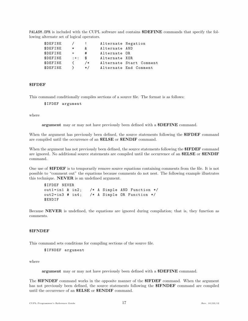
PALASM.OPR is included with the CUPL software and contains $DEFINE commands that specify the fol-lowing alternate set of logical operators.
$DEFINE / ! Alternate Negation
$DEFINE * & Alternate AND
$DEFINE + # Alternate OR
$DEFINE :+: $ Alternate XOR
$DEFINE { /* Alternate Start Comment
$DEFINE } */ Alternate End Comment
$IFDEF
This command conditionally compiles sections of a source file. The format is as follows:
$IFDEF argument
where
argument may or may not have previously been defined with a $DEFINE command.
When the argument has previously been defined, the source statements following the $IFDEF commandare compiled until the occurrence of an $ELSE or $ENDIF command.
When the argument has not previously been defined, the source statements following the $IFDEF commandare ignored. No additional source statements are compiled until the occurrence of an $ELSE or $ENDIFcommand.
One use of $IFDEF is to temporarily remove source equations containing comments from the file. It is notpossible to “comment out” the equations because comments do not nest. The following example illustratesthis technique. NEVER is an undefined argument.
$IFDEF NEVER
out1=in1 & in2; /* A Simple AND Function */
out2=in3 # in4; /* A Simple OR Function */
$ENDIF
Because NEVER is undefined, the equations are ignored during compilation; that is, they function ascomments.
$IFNDEF
This command sets conditions for compiling sections of the source file.
$IFNDEF argument
where
argument may or may not have previously been defined with a $DEFINE command.
The $IFNDEF command works in the opposite manner of the $IFDEF command. When the argumenthas not previously been defined, the source statements following the $IFNDEF command are compileduntil the occurrence of an $ELSE or $ENDIF command.
CUPL Programmer’s Reference Guide 17 Rev. 10/23/12

If the argument has previously been defined, the source statements following the $IFNDEF command areignored. No additional source statements are compiled until the occurrence of an $ELSE or $ENDIFcommand.
One use of $IFNDEF is to create a single source file containing two mutually exclusive sets of equations.Using an $IFNDEF and $ENDIF command to set off one of the sets of equations, quick toggling is possiblebetween the two sets of equations by defining or not defining the argument specified in the $IFNDEFcommand.
For example, some devices contain common output enable pins that directly control all the tri-state buffers,whereas other devices contain single product terms to enable each tri-state buffer individually. In thefollowing example, the argument, COMMON OE has not been defined, so the equations that follow arecompiled. Any equations following $ENDIF are not compiled.
$IFNDEF COMMON_OE
pin 11 = !enable; /* input pin for OE */
[q3,q2,q1,q0].oe = enable; /* assign tri -state */
/* equation for 4 */
/* outputs */
$ENDIF
If the device has common output enables, no equations are required to describe it. Therefore, in the aboveexample, for a device with common output enables, define COMMON OE so the compiler skips theequations between $IFNDEF and $ENDIF.
$ENDIF
This command ends a conditional compilation started with the $IFDEF or $IFNDEF commands. Theformat is as follows:
$ENDIF
The statements following the $ENDIF command are compiled in the same way as the statements precedingthe $IFDEF or $IFNDEF commands. Conditional compilation may be nested, and for each level of nestingof the $IFDEF or $IFNDEF command, an associated $ENDIF must be used.
The following example illustrates the use of $ENDIF with multiple levels of nesting.
$IFDEF prototype_1
pin 1 = set; /* Set on pin 1 */
pin 2 = reset; /* Reset on pin 2 */
$IFDEF prototype_2
pin 3 = enable; /* Enable on pin 3 */
pin 4 = disable; /* Disable on pin 4 */
$ENDIF
pin 5 = run; /* Run on pin 5 */
pin 6 = halt; /* Halt on pin 6 */
$ENDIF
CUPL Programmer’s Reference Guide 18 Rev. 10/23/12

$ELSE
This command reverses the state of conditional compilation as defined with $IFDEF or $IFNDEF. Theformat is as follows:
$ELSE
If the tested condition of the $IFDEF or $IFNDEF commands is true (that is, the statements followingthe command are compiled), then any source statements between an $ELSE and $ENDIF command areignored.
If the tested condition is false, then any source statements between the $IFDEF or $IFNDEF and $ELSEcommand are ignored, and statements following $ELSE are compiled.
For example, many times the production printed circuit board uses a different pinout than does the wire-wrap prototype. In the following example, since Prototype has been defined, the source statements following$IFDEF are compiled and the statements following $ELSE are ignored.
$DEFINE Prototype X /* define Prototype */
$IFDEF Prototype
pin 1 = memreq; /* memory request on */
/* pin 1 of prototype */
pin 2 = ioreq; /* I/O request on*/
/* pin 2 of prototype */
$ELSE
pin 1 = ioreq; /* I/O request on*/
/* pin 1 of PCB*/
pin 2 = memreq; /* memory request on */
/* pin 2 of PCB*/
$ENDIF
To compile the statements following $ELSE, remove the definition of Prototype.
$REPEAT
This command is similar to the FOR statement in C language and DO statements in FORTRAN language.It allows the user to duplicate repeat body by index. The format is as follows:
$REPEAT index=[number1 ,number2 ,... numbern]
repeat body
$REPEND
where n can be any number in the range 0 to 1023
In preprocessing, the repeat body will be duplicated from number1 to numbern. The index number can bewritten in short form as [number1..numbern] if the number is consecutive. The repeat body can be anyCUPL statement. Arithmetic operations can be performed in the repeat body. The arithmetic expressionmust be enclosed by braces { }.
For example, design a three to eight decoder.
FIELD sel = [in2 ..0]
$REPEAT i = [0..7]
CUPL Programmer’s Reference Guide 19 Rev. 10/23/12

!out{i} = sel:’h’{i} & enable;
$REPEND
Where index variable i goes from 0 to 7, so the statement “out{i} = sel:’h’{i} &enable;” will be repeatedduring preprocessing and create the following statements:
FIELD sel = [in2 ..0];
!out0 = sel:’h’0 & enable;
!out1 = sel:’h’1 & enable;
!out2 = sel:’h’2 & enable;
!out3 = sel:’h’3 & enable;
!out4 = sel:’h’4 & enable;
!out5 = sel:’h’5 & enable;
!out6 = sel:’h’6 & enable;
!out7 = sel:’h’7 & enable;
The following example shows how the arithmetic operation addition (+) and modulus (%) are used in therepeat body.
/* Design a five bit counter with a control signal advance.
If advance is high , counter is increased by one .*/
FIELD count[out4 ..0]
SEQUENCE count {
$REPEAT i = [0..31]
PRESENT S{i}
IF advance & !reset NEXT
S{(i+1)%(32)};
IF reset NEXT S{0};
DEFAULT NEXT S{i};
$REPEND
}
$REPEND
This command ends a repeat body that was started with $REPEAT. The format is as follows:
$REPEND
The statements following the $REPEND command are compiled in the same way as the statements pre-ceding the $REPEAT command. For each $REPEAT command, an associated $REPEND commandmust be used.
$MACRO
This command creates user-defined macros. The format is as follows:
$MACRO name argument1 argument2 ... argumentn
macro function body
$MEND
CUPL Programmer’s Reference Guide 20 Rev. 10/23/12

The macro function body will not be compiled until the macro name is called. The function is called bystating function name and passing the parameters to the function.
Like the $REPEAT command, the arithmetic operation can be used inside the macro function body andmust be enclosed in braces.
The following example illustrates how to use the $MACRO command.
Use the $MACRO command to define a decoder function with an arbitrary number of bits. This exampleplaces the macro definition and call in the same file.
$MACRO decoder bits MY_X MY_Y MY_enable;
FIELD select = [MY_Y{bits -1}..0];
$REPEAT i = [0..{2**( bits -1)}]
!MY_X{i} = select:’h’{i} & MY_enable;
$REPEND
$MEND
.../* Other statements */
decoder(3, out , in , enable ); /* macro function call*/
Calling function decoder will create the following statements by macro expansion.
FIELD sel = [in2 ..0];
!out0 = sel:’h’0 & enable;
!out1 = sel:’h’1 & enable;
!out2 = sel:’h’2 & enable;
!out3 = sel:’h’3 & enable;
!out4 = sel:’h’4 & enable;
!out5 = sel:’h’5 & enable;
!out6 = sel:’h’6 & enable;
!out7 = sel:’h’7 & enable;
When macros are called, the keyword NC is used to represent no connection. Because NC is a keyword, theletters NC should not be used as a variable elsewhere in CUPL.
A macro expansion file can be created by using the “-e” flag when compiling the PLD file. CUPL will createan expanded macro file with the same name as the PLD file, with the extension “.mx”.
The macro definition can be stored in a separate file with a “.m” extension. Using the $INCLUDEcommand, specify the file. All the macro functions in that file will then be accessible. The following exampleshows the macro definition and calling statement stored in different files.
The macro definition of decoder is stored in the file “macrolib.m”
$INCLUDE macrolib.m /* specify the macro library */
.../* other statements */
decoder(4, out , in enable );
.../* other statements */
More examples can be found in the example files provided on diskette.
CUPL Programmer’s Reference Guide 21 Rev. 10/23/12

Operator Example Description Precedence! !A NOT 1& A & B AND 2# A # B OR 3$ A $ B XOR 4
Table 1.8: Precedence of Logical Operators
Operator Example Description Precedence** 2**3 Exponentiation 1* 2*i Multiplication 2/ 4/2 Division 2% 9%8 Modulus 2+ 2+4 Addition 3- 4-i Subtraction 3
Table 1.9: Precedence of Arithmetic Operators
$MEND
This command ends a macro function body started with $MACRO. The format is as follows:
$MEND
The statements following the $MEND command are compiled in the same way as the statements precedingthe $MACRO command. For each $MACRO command, an associated $MEND command.must be used.
1.2 Language Syntax
This section describes the CUPL language syntax. It explains how to use logic equations, truth tables, statemachine syntax, condition syntax and user-defined functions to create a PLD design.
1.2.1 Logical Operators
CUPL supports the four standard logical operators used for boolean expressions. Table 1.8 lists theseoperators and their order of precedence, from highest to lowest.
The truth tables in Figure 1.5 list the Boolean Logic rules for each operator.
1.2.2 Arithmetic Operators
CUPL supports six standard arithmetic operators used for arithmetic expressions. The arithmetic expressionscan only be used in the $REPEAT and $MACRO commands. Arithmetic expressions must appear inbraces { }. Table 1.9 lists these operators and their order of precedence, from highest to lowest.
CUPL Programmer’s Reference Guide 22 Rev. 10/23/12

NOT : ones complement !
0 11 0
A !A
AND &
0 0 00 1 01 0 01 1 1
A B A & B
OR #
0 0 00 1 11 0 11 1 1
A B A # B
XOR : exclusive OR $
0 0 00 1 11 0 11 1 0
A B A $ B
Figure 1.5: Truth Tables
Function Base
LOG2 Binary
LOG8 Octal
LOG16 Hexadecimal
LOG Decimal
Table 1.10: Arithmetic Function
1.2.3 Arithmetic Function
CUPL supports one arithmetic function used for arithmetic expressions. The arithmetic expressions canonly be used in the $REPEAT and $MACRO commands. Table 1.10 lists the function.
The LOG function returns an integer value. For example:
LOG2 (32) = 5 <==> 2**5 = 32
LOG2 (33) = ceil (5.0444) = 6 <==> 2**6 = 64
Ceil(x) returns the smallest integer not less than x.
1.2.4 Extensions
Extensions can be added to variable names to indicate specific functions associated with the major nodesinside a programmable device, including such capabilities as flip-flop description and programmable three-state enables. Table 1.11 lists the extensions that are supported by CUPL and on which side of the equalsign (=) they are used. The compiler checks the usage of the extension to determine whether it is valid forthe specified device and whether its usage conflicts with some other extension used.
CUPL Programmer’s Reference Guide 23 Rev. 10/23/12

Extension Used Side Description.AP L Asynchronous preset of flip-flop.AR L Asynchronous reset of flip-flop.APMUX L Asynchronous preset multiplexer selection.ARMUX L Asynchronous reset multiplexer selection.BYP L Programmable register bypass.CA L Complement array.CE L CE input of enabled D-CE type flip-flop.CK L Programmable clock of flip-flop.CKMUX L Clock multiplexer selection.D L D nput of D-type flip-flop.DFB R D registered feedback path selection.DQ R Q output of D-type flip-flop.IMUX L Input multiplexer selection of two pins.INT R Internal feedback path for registered macrocell.IO R Pin feedback path selection.IOAR L Asynchronous reset for pin feedback register.IOAP L Asynchronous preset for pin feedback register.IOCK L Clock for pin feedback register.IOD R Pin feedback path through D register.IOL R Pin feedback path through latch.IOSP L Synchronous preset for pin feedback register.IOSR L Synchronous reset for pin feedback register.J L J input of JK-type output flip-flop.K L K input of JK-type output flip-flop.L L D input of transparent latch.LE L Programmable latch enable.LEMUX L Latch enable multiplexer selection.LFB R Latched feedback path selection.LQ R Q output of transparent input latch.OBS L Programmable observability of buried nodes.OE L Programmable output enable.OEMUX L Tri-state multiplexer selection.PR L Programmable preload.R L R input of SR-type output flip-flop.S L S input of SR-type output flip-flop.SP L Synchronous preset of flip-flop.SR L Synchronous reset of flip-flop.T L T input of toggle output flip-flop.TEC L Technology-dependent fuse selection.TFB R T registered feedback path selection.T1 L T1 input of 2-T flip-flop.T2 L T2 input of 2-T flip-flop
Table 1.11: Extensions
CUPL Programmer’s Reference Guide 24 Rev. 10/23/12

Each extension provides access to a specific function. For example, to specify an equation for output enable(on a device that has the capability) use the .OE extension. The equation will look as follows:
PIN 2 = A;
PIN 3 = B;
PIN 4 = C;
PIN 15 = VARNAME;
VARNAME.OE = A&B;
Note that the compiler supports only the flip-flop capabilities that are physically implemented in the device.For example, the compiler does not attempt to emulate a JK-type flip-flop in a device that only has D-typeregisters. Any attempt to use capabilities not present in a device will cause the compiler to report an error.
For those devices containing bi-directional I/O pins with programmable output enables, CUPL automaticallygenerates the output enable expression according to the usage of the pin. If the variable name is used onthe left side of an equation, the pin is assumed to be an output and is assigned binary value 1; that is, theoutput enable expression is defaulted to the following:
PIN_NAME.OE=’b’1; /* Tri -state buffer */
/* Always ON */
Those pins that are used only as inputs (that is, the variable name appears only on the right side of anequation) are assigned binary value 0; the output enable expression is defaulted to the following:
PIN_NAME.OE = ’b’0; /* Tri -state buffer
Always OFF */
When the I/O pin is to be used as both an input and output, any new output enable expression that theuser specifies overrides the default to enable the tri-state buffer at the desired time.
When using a JK or SR-type flip-flop, an equation must be written for both the J and K (or S and R) inputs.If the design does not require an equation for one of the inputs, use the following construct to turn off theinput:
COUNT0.J=’b’0 ; /* J input not used */
Control functions such as asynchronous resets and presets are commonly connected to a group (or all) ofthe registers in a device. When an equation is written for one of these control functions, it is actually beingwritten for all of the registers in the group. For documentation purposes, CUPL checks for the presenceof such an equation for each register in the group and generates a warning message for any member of thegroup that does not have an identical equation. If all the control functions for a given group are defined withdifferent equations, the compiler will generate an error since it cannot decide which equation is the correctone. Remember that this is a device specific issue and it is a good idea to understand the capability of thedevice being used.
Figure 1.6 shows the use of extensions. Note that this figure does not represent an actual circuit, but showshow to use extensions to write equations for different functions in a circuit.
The figure shows an equation with a .D extension that has been written for the output to specify it as aregistered output. Note that when feedback (OUT_VAR) is used in an equation, it does not have an extension.
.Note: The DQ extension is used for input pins only
Additional equations can be written to specify other types of controls and control points. For example, anequation for the output enable can be written as follows:
CUPL Programmer’s Reference Guide 25 Rev. 10/23/12

FUSEARRAY
OUT_VAR.OE
OUT_VAR.SP
OUT_VAR.D
OUT_VAR.CK
OUT_VAR.AR
OUT_VAR
OUT_VAR (default feedback)
OUT_VAR.IO (alternate feedback)
SP
AR
D Q
Q
n
IN_VAR1
IN_VAR2
IN_VAR3D Q
IN_VAR3.DQ
OUT_VAR.D = IN_VAR1 & OUT_VAR # !IN_VAR2 & IN_VAR3.DQ # !IN_VAR1 & OUT_VAR.IO
Figure 1.6: Circuit Illustrating Extensions
Figure 1.7: Programmable Feedback
OUT_VAR.OE = IN_VAR1 # IN_VAR2
1.2.5 Feedback Extensions Usage
Certain devices can program the feedback path. For example, the EP300 contains a multiplexer for eachoutput that allows the feedback path to be selected as internal, registered, or pin feedback.
Figure 1.7 shows the EP300 programmable feedback capability.
CUPL automatically chooses a default feedback path according to the usage of the output. For example, ifthe output is used as a registered output, then the default feedback path will be registered, as in Figure 1.6.This default can be overridden by adding an extension to the feedback variables. For example, by addingthe .IO extension to the feedback variables of a registered output, CUPL will select the pin feedback path.
Figure 1.8 shows a registered output with pin feedback.
CUPL Programmer’s Reference Guide 26 Rev. 10/23/12

Figure 1.8: Programmable Pin (I/O) Feedback
Figure 1.9: Programmable Registered Feedback
Figure 1.9 shows a combinatorial output with registered feedback.
Figure 1.10 shows a combinatorial output with internal feedback.
1.2.6 Multiplexer Extension Usage
Certain devices allow selection between programmable and common control functions. For example, for eachoutput, the P29MA16 contains multiplexers for selecting between common and product term clocks andoutput enables.
Figure 1.11 shows the P29MA16 programmable clock and output enable capability.
If expressions are written for the .OE and .CK extensions, the multiplexer outputs are selected as product
Figure 1.10: Programmable Internal Feedback
CUPL Programmer’s Reference Guide 27 Rev. 10/23/12

Figure 1.11: Output with Output Enable and Clock Multiplexers
Figure 1.12: Output with Output Enable and Clock Multiplexers Selected
term output enable and clock, respectively. Otherwise, if expressions are written for the .OEMUX and .CKMUX
extensions, the multiplexer outputs are selected as common output enable and clock, respectively.
Expressions written for the .OEMUX and .CKMUX extensions can have only one variable and be operated ononly by the negation operator, !. This is because their inputs are not from the fuse array, but from a commonsource, such as a clock pin. This is in contrast with expressions written for the .OE and .CK extensions,which take their inputs from the fuse array.
Figure 1.12 shows a registered output with the output enable multiplexer output selected as Vcc, outputenable always enabled, and the clock multiplexer output selected as the common clock pin inverted, negative-edge clock.
Expressions for the .OE and .OEMUX extensions are mutually exclusive; that is, only one may be written foreach output. Likewise, expressions for the .CK and .CKMUX extensions are mutually exclusive.
1.2.7 Extension Usage
This section contains diagrams and explanations for all the variable extensions.
CUPL Programmer’s Reference Guide 28 Rev. 10/23/12
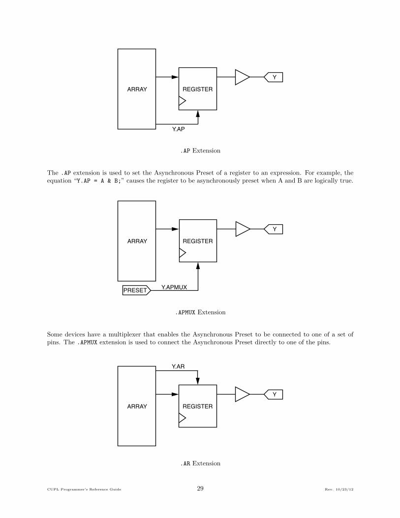
ARRAY
Y
REGISTER
Y.AP
.AP Extension
The .AP extension is used to set the Asynchronous Preset of a register to an expression. For example, theequation “Y.AP = A & B;” causes the register to be asynchronously preset when A and B are logically true.
ARRAY
Y
PRESET
REGISTER
Y.APMUX
.APMUX Extension
Some devices have a multiplexer that enables the Asynchronous Preset to be connected to one of a set ofpins. The .APMUX extension is used to connect the Asynchronous Preset directly to one of the pins.
ARRAY
Y
REGISTER
Y.AR
.AR Extension
CUPL Programmer’s Reference Guide 29 Rev. 10/23/12

The .AR extension is used to define the expression for Asynchronous Reset for a register. This is used indevices that have one or more product terms connected to the Asynchronous Reset of the register.
ARRAY
Y
RESET
REGISTER
Y.ARMUX
.ARMUX Extension
In devices that have a multiplexer for connecting the Asynchronous Reset of a register directly to one ormore pins, the .ARMUX extension is used to make the connection. It is possible that a device may have thecapability to have Asynchronous Reset connected either to a pin or to a product term. In this case, the .AR
extension is used to select the product term connection, whereas, the .ARMUX extension is used to connectthe pin.
ARRAY
Y.CA
Y
.CA Extension
The .CA extension is used in a few special cases where devices have complementa array nodes. Devices thathave this capability are the F501 and F502.(See Appendix B)
CUPL Programmer’s Reference Guide 30 Rev. 10/23/12

ARRAY
YD-CE
REGISTER
Y.D
Y.CE
D
CE
.CE Extension
The .CE extension is used for D-CE registers. It serves to specify the input to the CE of the register. Indevices that have D-CE registers, and the CE terms are not used, they must be set to binary 1 so that theregisters behave the same as D registers. Failure to enable the CE terms will result in D registers that neverchange state.
ARRAY
YREGISTER
Y.CK
.CK Extension
The .CK extension is used to select a product term driven clock. Some devices have the capability to connectthe clock for a register to one or more pins or to a product term. The .CK extension will select the productterm. To connect the clock to a pin directly, use the .CKMUX extension.
ARRAY
Y
CLK
REGISTER
Y.CKMUX
.CKMUX Extension
CUPL Programmer’s Reference Guide 31 Rev. 10/23/12

The .CKMUX extension is used to connect the clock input of a register to one of a set of pins. This is neededbecause some devices have a multiplexer for connecting the clock to one of a set of pins. This does not meanthat the clock may be connected to any pin. Typically, the multiplexer will allow the clock to be connectedto one of two pins. Some devices have a multiplexer for connecting to one of four pins.
ARRAY
YD
REGISTER
Y.D
.D Extension
The .D extension is used to specify the D input to a D register. The use of the .D register actually causesthe compiler to configure programmable macrocells as D registers. For outputs that have only D registeredoutput, the .D extension must be used. If the .D extension is used for an output that does not have true Dregisters, the compiler will generate an error.
ARRAY
YD
REGISTER
Y.DFB
.DFB Extension
The .DFB extension is used in special cases where a programmable output macrocell is configured as com-binatorial but the D register still remains connected to the output. The .DFB extension provides a meansto use the feedback from the register. Under normal conditions, when an output is configured as registered,the feedback from the register is selected by not specifying an extension.
CUPL Programmer’s Reference Guide 32 Rev. 10/23/12

ARRAY
AD
REGISTER
A.DQ
.DQ Extension
The .DQ extension is used to specify an input D register. Use of the .DQ extension actually configures theinput as registered. The .DQ extension is not used to specify Q output from an output D register.
ARRAY
Y
REGISTER
Y.IMUX
Z
REGISTER
!Y.IMUX
.IMUX Extension
The .IMUX extension is an advanced extension which is used to select a feedback path. This is used in devicesthat have pin feedback from two I/O pins connected to a multiplexer. Only one of the pins may use thefeedback path.
CUPL Programmer’s Reference Guide 33 Rev. 10/23/12

ARRAY
Y
Z
REGISTER
Y.INT
Y
Z.INT
Z.IOZ
.INT Extension
The .INT extension is used for selecting an internal feedback path. This could be used for combinatorial orregistered output. The .INT extension provides combinatorial feedback.
ARRAY
Y
REGISTER
YY.IO
.IO Extension
The .IO extension is used to select pin feedback when the macrocell is configured as registered.
CUPL Programmer’s Reference Guide 34 Rev. 10/23/12

ARRAY
YMACRO
CELLMACRO
CELL
Y.IOAP
REGISTER
.IOAP Extension
The .IOAP extension is used to specify the expression for Asynchronous Preset in cases where there isregistered pin feedback from an output macrocell.
ARRAY
YMACRO
CELLMACRO
CELL
Y.IOAR
REGISTER
.IOAR Extension
The .IOAR extension is used to specify the expression for Asynchronous Reset.in cases where there is regis-tered pin feedback from an output macrocell.
CUPL Programmer’s Reference Guide 35 Rev. 10/23/12

ARRAY
YMACRO
CELLMACRO
CELL
CLK
REGISTER
Y.IOCK
.IOCK Extension
The .IOCK extension is used to specify a clock expression for a registered pin feedback that is connected toan output macrocell.
ARRAY
YMACRO
CELL
REGISTERD
Y.IOD
.IOD Extension
CUPL Programmer’s Reference Guide 36 Rev. 10/23/12

The .IOD extension is used to specify feedback from a register that is connected to an output macrocell bythe pin feedback path.
ARRAY
YMACRO
CELL
LATCH
L
Y.IOL
.IOL Extension
The .IOL extension is used to specify feedback from a buried latch that is connected to an output macrocellby the pin feedback path.
ARRAY
YMACRO
CELLMACRO
CELL
Y.IOSP
REGISTER
.IOSP Extension
CUPL Programmer’s Reference Guide 37 Rev. 10/23/12

The .IOSP extension is used to specify the expression for Synchronous Preset in cases where there is registeredpin feedback from an output macrocell.
ARRAY
YMACRO
CELLMACRO
CELL
Y.IOSR
REGISTER
.IOSR Extension
The .IOSR extension is used to specify the expression for Synchronous Reset in cases where there is registeredpin feedback from an output macrocell.
ARRAY
YJ-K
REGISTER
Y.J
Y.K
J
K
.J and .K Extension
The .J and .K extensions are used to specify J and K input to a JK register. The use of the .J and the.K extensions actually cause the compiler to configure the output as JK, if the macrocell is programmable.Equations for both J and K must be specified. If one of the inputs is not used, it must be set to binary 0 todisable it.
CUPL Programmer’s Reference Guide 38 Rev. 10/23/12

ARRAY
Y
LATCH
LY.L
.L Extension
The .L extension is used to specify input into a Latch. In devices with programmable macrocells, the use ofthe .L extension causes the compiler to configure the macrocell as a latched output.
ARRAY
YL-LE
REGISTER
Y.L
Y.LE
L
LE
.LE Extension
The .LE extension is used to specify the latch enable equation for a latch. The .LE extension causes aproduct term to be connected to the latch enable.
ARRAY
Y
ENABLE
LATCH
Y.LEMUX
.LEMUX Extension
The .LEMUX extension is used to specify a pin connection for the latch enable.
CUPL Programmer’s Reference Guide 39 Rev. 10/23/12

ARRAY
Y
Y.LFB
LATCH
.LFB Extension
The .LFB extension is used in special cases where a programmable output macrocell is configured as combi-natorial but the latch still remains connected to the output. The .LFB extension provides a means to use thefeedback from the latch. Under normal conditions, when an output is configured as latched, the feedbackfrom the latch is selected by using no extension.
ARRAY
AL
LATCH
A.LQ
.LQ Extension
The .LQ extension is used to specify an input latch. Use of the .LQ extension actually configures the inputas latched. The .LQ extension is not used to specify Q output from an output latch.
ARRAY
Y
Y.OE
MACROCELL
.OE Extension
The .OE extension is used to specify a product term driven output enable signal.
CUPL Programmer’s Reference Guide 40 Rev. 10/23/12

ARRAYY
Y.OEMUX
YMACRO
CELL
ENA
Y.OE
.OEMUX Extension
The .OEMUX extension is used to connect the output enable to one of a set of pins. This is needed becausesome devices have a multiplexer for connecting the output enable to one of a set of pins. This does not meanthat the output enable may be connected to any pin. Typically, the multiplexer will allow the output enableto be connected to one of two pins. Some devices have a multiplexer for connecting to one of four pins.
ARRAY
YS-R
REGISTER
Y.S
Y.R
S
R
.S and .R Extension
The .S and .R extensions are used to specify S and R input to a SR register. The use of the .S and the.R extensions actually cause the compiler to configure the output as SR, if the macrocell is programmable.Equations for both S and R must be specified. If one of the inputs is not used, it must be set to binary 0 todisable it.
ARRAY
Y
REGISTER
Y.SP
CUPL Programmer’s Reference Guide 41 Rev. 10/23/12

.SP Extension
The .SP extension is used to set the Synchronous Preset of a register to an expression. For example, theequation “Y.SP = A & B;” causes the register to be synchronously preset when A and B are logically true.
ARRAY
Y
REGISTER
Y.SR
.SR Extension
The .SR extension is used to define the expression for Synchronous Reset for a register. This is used indevices that have one or more product terms connected to the Synchronous Reset of the register.
ARRAY
YT
REGISTER
Y.T
.T Extension
The .T extension specifies the T input for a T register. The use of the T extension itself causes the compilerto configure the macrocell as a T register. Special consideration should be given to devices with T registersand programmable polarity before the register. Since T registers toggle when the incoming signal is true,the behavior will be changed when the polarity is changed since the incoming signal is now inverted beforereaching the register. It is best to declare pins that will use T registers as active high always.
CUPL Programmer’s Reference Guide 42 Rev. 10/23/12

Commutative Property: A & B = B & A
A # B = B # A
Associative Property: A & (B & C) = (A & B) & C
A # (B # C) = (A # B) # C
Distributive Property: A & (B # C) = (A & B) # (A & C)
A # (B & C) = (A # B) & (A # C)
Absorptive Property: A & (A # B) = A
A # (A & B) = A
DeMorgan’s Theorem: !(A & B & C) = !A # !B # !C
!(A # B # C) = !A & !B & !C
XOR Identity: A $ B = (!A & B) # (A & !B)
!(A $ B) = A $ !B = !A $ B= (!A & !B) # (A& B)
Theorems: A & 0 = 0 A & 1 = A
A # 0 = A A # 1 = 1
A & A = A A & !A = 0
A # A = A A # !A = 1
Table 1.12: Logic Evaluation Rules
ARRAY
YT
REGISTER
Y.TFB
.TFB Extension
The .TFB extension is used in special cases where a programmable output macrocell is configured as com-binatorial but the T register still remains connected to the output. The .TFB extension provides a meansto use the feedback from the register. Under normal conditions, when an output is configured as registered,the feedback from the register is selected by using no extension.
1.2.8 Logic Expressions
Table 1.12 lists the rules that the CUPL compiler uses for evaluating logic expressions. These basic rulesare listed for reference purposes only.
Expressions are combinations of variables and operators that produce a single result when evaluated. Anexpression may be composed of any number of sub-expressions.
Expressions are evaluated according to the precedence of the particular operators involved. When operatorswith the same precedence appear in an expression, evaluation order is taken from left to right. Parenthesesmay be used to change the order of evaluation; the expression within the innermost set of parentheses isevaluated first.
CUPL Programmer’s Reference Guide 43 Rev. 10/23/12

Expression Result CommentsA # B & C A #
B & C
(A # B) & C A & C Parentheses change order#
B & C
!A & B !A & B
!(A & B) !A # !B DeMorgan’s TheoremA # B & C # D A #
D #
B & C
A # B & (C # D) A # Parentheses change orderB & C
#
B & D
Table 1.13: Sample Expressions
In Table 1.13, note how the order of evaluation and use of parentheses affect the value of the expression.
1.2.9 Logic Equations
Logic equations are the building blocks of the CUPL language. The form for logic equations is as follows:
[!] var [.ext] = exp ;
where
var is a single variable or a list of indexed or non-indexed variables defined according to therules for the list notation (see Sec. 1.1.6, List Notation). When a variable list is used, theexpression is assigned to each variable in the list.
.ext is an optional extension to assign a function to the major nodes inside a programmabledevice (see Table 1.11).
exp is an expression; that is, a combination of variables and operators (see “Expressions” in thischapter).
= is the assignment operator; it assigns the value of an expression to a variable or set ofvariables.
! is the complement operator.
The complement operator can be used to express the logic equation in negative true logic. The operatordirectly precedes the variable name (no spaces) and denotes that the expression on the right side is to becomplemented before it is assigned to the variable name. Use of the complement operator on the left side isprovided solely as a convenience. The equation may just as easily be written by complementing the entireexpression on the right side.
Older logic design software that did not provide the automatic DeMorgan capability (output polarity assignedaccording to the pin variable declaration) required the use of the complement operator when using deviceswith inverting buffers.
Place logic equations in the “Logic Equation” section of the source file provided by the template file.
CUPL Programmer’s Reference Guide 44 Rev. 10/23/12

Logic equations are not limited solely to pin (or node) variables, but may be written for any arbitraryvariable name. A variable defined in this manner is an intermediate variable. An intermediate variable namecan be used in other expressions to generate logic equations or additional intermediate variables. Writinglogic equations in this “top down” manner yields a logic description file that is generally easier to read andcomprehend.
Place intermediate variables in the “Declarations and Intermediate Variable Definitions” section of the sourcefile.
The following are some examples of logic equations:
SEL_0=A15 & !A14; /* A simple , decoded output pin */
Q0.D=Q1 & Q2 & Q3; /* Output pin w/ D flip -flop */
Q1.J = Q2 # Q3; /* Output pin w/ JK flip -flop */
Q1.K = Q2 & !Q3;
MREQ=READ # WRITE; /* Intermediate Variable */
SEL_1=MREQ & A15; /* Output intermediate var */
[D0..3] = ’h’FF; /* Data bits assigned to constant */
[D0..3]. oe = read; /* Data bits assigned to variable */
APPEND Statements
In standard logic equations, normally only one expression is assigned to a variable. The APPEND statementenables multiple expressions to be assigned to a single variable. The format is as follows.
APPEND [!] var[.ext] = expr ;
where
! is the complement operator to optionally define the polarity of the variable.
var is a single variable or a list of indexed or non-indexed variables in standard list format.
.ext is an optional extension that defines the function of the variable.
= is the assignment operator.
expr is a valid expression.
; is a semicolon to mark the end of the statement.
The expression that results from multiple APPEND statements is the logical OR of all the APPEND state-ments. If an expression has not already been assigned to the variable, the first APPEND statement is treatedas the first assignment.
The following example shows several APPEND statements.
APPEND Y = A0 & A1 ;
APPEND Y = B0 & B1 ;
APPEND Y = C0 & C1 ;
The three statements above are equivalent to the following equation.
Y = (A0 & A1) # (B0 & B1) # (C0 & C1) ;
CUPL Programmer’s Reference Guide 45 Rev. 10/23/12

The APPEND statement is useful in adding additional terms (such as reset) to state-machine variablesor constructing user-defined functions (see Sec 1.3.2, State Machine Syntax and Sec. 1.3.4, User-DefinedFunctions).
1.2.10 Set Operations
All operations that are performed on a single bit of information, for example, an input pin, a register, oran output pin, may be applied to multiple bits of information grouped into sets. Set operations can beperformed between a set and a variable or expression, or between two sets.
The result of an operation between a set and a single variable (or expression) is a new set in which theoperation is performed between each element of the set and the variable (or expression). For example
[D0, D1, D2, D3] & read
evaluates to:
[D0 & read , D1 & read , D2 & read , D3 & read]
When an operation is performed on two sets, the sets must be the same size (that is, contain the samenumber of elements). The result of an operation between two sets is a new set in which the operation isperformed between elements of each set.
For example
[A0, A1, A2, A3] & [B0, B1, B2, B3]
evaluates to:
[A0 & B0, A1 & B1, A2 & B2, A3 & B3]
Bit field statements (see Sec. 1.1.11, Bit Field Declaration Statements) may be used to group variables intoa set that can be referenced by a single variable name. For example, group the two sets of variables in theabove operation as follows:
FIELD a_inputs = [A0, A1, A2 A3] ;
FIELD b_inputs = [B0, B1, B2, B3] ;
Then perform a set operation between the two sets, for example, an AND operation, as follows:
a_inputs & b_inputs
When numbers are used in set operations, they are treated as sets of binary digits. A single octal numberrepresents a set of three binary digits, and a single decimal or hexadecimal number represents a set of fourbinary digits. Table 1.14 lists the representation of numbers as sets.
Numbers may be effectively used as “bit masks” in logic equations using sets. An example of this applicationis the following 4-bit counter.
field count = [Q3, Q2, Q1, Q0];
count.d = ’b’ 0001 & (!Q0)
# ’b’ 0010 & (Q1 $ Q0)
# ’b’ 0100 & (Q2 $ Q1 & Q0)
# ’b’ 1000 & (Q3 $ Q2 & Q1 & Q0);
CUPL Programmer’s Reference Guide 46 Rev. 10/23/12

Octal Equivalent Decimal Equivalent Hexadecimal Equivalent
Number Binary Set Number Binary Set Number Binary Set
’O’X [X, X, X] ’H’X [X,X,X,X]
’O’0 [0, 0, 0] ’D’0 [0,0,0,0] ’H’0 [0,0,0,0]
’O’1 [0, 0, 1] ’D’1 [0,0,0,1] ’H’1 [0,0,0,1]
’O’2 [0, 1, 0] ’D’2 [0,0,1,0] ’H’2 [0,0,1,0]
’O’3 [0, 1, 1] ’D’3 [0,0,1,1] ’H’3 [0,0,1,1]
’O’4 [1, 0, 0] ’D’4 [0,1,0,0] ’H’4 [0,1,0,0]
’O’5 [1, 0, 1] ’D’5 [0,1,0,1] ’H’5 [0,1,0,1]
’O’6 [1, 1, 0] ’D’6 [0,1,1,0] ’H’6 [0,1,1,0]
’O’7 [1, 1, 1] ’D’7 [0,1,1,1] ’H’7 [0,1,1,1]
’D’8 [1,0,0,0] ’H’8 [1,0,0,0]
’D’9 [1,0,0,1] ’H’9 [1,0,0,1]
’H’A [1,0,1,0]
’H’B [1,0,1,1]
’H’C [1,1,0,0]
’H’D [1,1,0,1]
’H’E [1,1,1,0]
’H’F [1,1,1,1]
Table 1.14: Equivalent Binary Sets
The equivalent logic equations written without set notation are as follows:
Q0.d = !Q0;
Q1.d = Q1 $ Q0;
Q2.d = Q2 $ Q1 & Q0;
Q3.d = Q3 $ Q2 & Q1 & Q0;
1.2.11 Equality Operations
Unlike other set operations, the equality operation evaluates to a single Boolean expression. It checks forbit equality between a set of variables and a constant. The format for the equality operation is as follows:
1. [var , var , ... var]: constant ;
2. bit_field_var:constant ;
where
[var, var, ... var ] is a list of variables in shorthand notation.
constant is a number (hexadecimal by default).
bit field var is a variable defined using a bit field statement.
: is the equality operator.
; is a semicolon used to mark the statement end.
.Note: Square brackets do not indicate optional items, but delimit variables in a list.
Format1 is used between a list of variables and a constant value. Format 2 is used between a bit field variableand a constant value.
CUPL Programmer’s Reference Guide 47 Rev. 10/23/12

The bit positions of the constant number are checked against the corresponding positions in the set. Wherethe bit position is a binary 1, the set element is unchanged. Where the bit position is a binary 0, the setelement is negated. Where the bit position is a binary X, the set element is removed. The resulting elementsare then ANDed together to create a single expression. In the following example, hexadecimal D (binary1101) is checked against A3, A2, A1, and A0.
select = [A3..0]:’h’D ;
The set elements A3, A2, and A0 remain unchanged because the corresponding bit position is one or true.Set element A1 is negated because its corresponding bit position is zero or false. Therefore, the aboveexpression is equivalent to the following expression:
select = A3 & A2 & !A1 & A0 ;
In the following example, binary 1X0X is checked against A3, A2, A1, A0.
select = [A3..0]:’b’1X0X ;
The set element A3 remains unchanged because the corresponding bit position is one or true. Set element A1is negated because its corresponding bit position is zero or false. Set elements A2 and A0 are removed fromthe expression because the corresponding bit positions are “don’t-cared.” Therefore, the above expression isequivalent to the following equation:
select = A3 & !A1 ;
In addition to address decoding, the equality operator can be used to specify a counter or state machine.For example, a 4-bit counter can be specified using the following notation:
FIELD count = [Q0..3];
Q0.J = count:0 # count:2 # count:4 # count:6
# count :8 # count:A # count:C # count:E ;
Q0.K = count:1 # count:3 # count:5 # count:7
# count :9 # count:B # count:D # count:F ;
Q1.J = count:1 # count:5 # count:9 # count:D ;
Q1.K = count:3 # count:7 # count:B # count:F ;
Q2.J = count:3 # count:B ;
Q2.K = count:7 # count:F ;
Q3.J = count:7 ;
Q3.K = count:F ;
The equality operator can also be used with a set of variables that are to be operated upon identically. Thefollowing syntax can be used as a time-saving convenience:
[var , var , ... , var]:op
which is equivalent to:
var op var op ... var
where
op is the &, # or $ operator (or its equivalent if an alternate set of operators has been defined).
var is any variable name.
For example, the following three expressions
CUPL Programmer’s Reference Guide 48 Rev. 10/23/12

[A3,A2,A1,A0]:&
[B3,B2,B1,B0]:#
[C3,C2,C1,C0]:$
are equivalent respectively to:
A3 & A2 & A1 & A0
B3 # B2 # B1 # B0
C3 $ C2 $ C1 $ C0
The equality operation can be used with an equivalent binary set to create a function table description ofthe output values. For example, in the following Binary-to-BCD code converter, output values are assignedby using the equality operation to define the inputs, and equivalent binary sets to group the output.
FIELD input = [in3 ..0] ;
FIELD output = [out4 ..0] ;
/* in3 ..0 -> out4 ..0*/
$DEFINE L ’b’0
$DEFINE H ’b’1
output = input :0 & [L, L, L, L, L]
# input :1 & [L, L, L, L, H]
# input :2 & [L, L, L, H, L]
# input :3 & [L, L, L, H, H]
# input :4 & [L, L, H, L, L]
# input :5 & [L, L, H, L, H]
# input :6 & [L, L, H, H, L]
# input :7 & [L, L, H, H, H]
# input :8 & [L, H, L, L, L]
# input :9 & [L, H, L, L, H]
# input:A & [H, L, L, L, L]
# input:B & [H, L, L, L, H]
# input:C & [H, L, L, H, L]
# input:D & [H, L, L, H, H]
# input:E & [H, L, H, L, L]
# input:F & [H, L, H, L, H];
$UNDEF L
$UNDEF H
1.2.12 Indexed Variables, Bit Fields and Equality
Indexed variables, field statements and the range function operate with each other in tight union. Thissection will attempt to illustrate this relationship.
As discussed earlier in this chapter, indexed variables can be used as an easy way to declare multiple variableswith few actual lines of code.
For example
Pin [2..4] = [AD0 ..2];
expands to:
CUPL Programmer’s Reference Guide 49 Rev. 10/23/12

Pin 2 = AD0;
Pin 3 = AD1;
Pin 4 = AD2;
The FIELD statement is used to group a set of related signals into one element. It works by using a 32 bitfield where each bit in the field represents one of the members of the field. If there are less than 32 membersthen the extra bits are ignored. For example:
Pin 2 = VAR_A;
Pin 3 = VAR_B;
Pin 4 = VAR_C;
Pin 15 = ROM_SEL;
FIELD ADDR = [VAR_A ,VAR_B ,VAR_C ];
The following figure shows how the variables VAR_A, VAR_B and VAR_C map into the bit field.
3 3 2 2 2 2 2 2 2 2 2 2 1 1 1 1 1 1 1 1 1 11 0 9 8 7 6 5 4 3 2 1 0 9 8 7 6 5 4 3 2 1 0 9 8 7 6 5 4 3 2 1 0
These bits are ignoredVAR_C
VAR_B
VAR_A
Figure 1.13: Bit field mapping of member variables
Now suppose that we had an output as follows:
ROM_SEL = ADDR :3;
The contents of the bit field for this equation would be as follows:
"XXXXXXXXXXXXXXXXXXXXXXXXXXXXX011"
This would result in the following equations:
ROM_SEL = !VAR_A & VAR_B & VAR_C;
When using indexed variables, the internal representation changes slightly. The index number of the variabledetermines its position in the bit field. Therefore, VAR0 always resides in bit position 0 regardless of thedeclaration of the field. The two following declarations both have the identical internal representation.
field ADDR = [VAR0 , VAR1 , VAR2];
field ADDR = [VAR2 , VAR1 , VAR0];
3 3 2 2 2 2 2 2 2 2 2 2 1 1 1 1 1 1 1 1 1 11 0 9 8 7 6 5 4 3 2 1 0 9 8 7 6 5 4 3 2 1 0 9 8 7 6 5 4 3 2 1 0
These bits are ignoredVAR_0
VAR_1
VAR_2
Figure 1.14: Bit field representation with indexed variables
Now suppose that we had an output as follows:
CUPL Programmer’s Reference Guide 50 Rev. 10/23/12

ROM_SEL = ADDR :3;
The contents of the bit field for this equation would be as follows:
"XXXXXXXXXXXXXXXXXXXXXXXXXXXXX011"
This would result in the following equations:
ROM_SEL = !VAR2 & VAR1 & VAR0;
If we take a set of variables that use a higher index we can see that the way indexed variables are handledmay affect the output differently than we expect. If the variables used are VAR17, VAR18 and VAR19 then thebit map changes accordingly. The equivalence with 3 now does not work because 3 only maps into bits 0, 1and 2. What needs to be done is to add zeroes to move the desired equivalence up to the desired range.
Now suppose that we had an output as follows:
FIELD ADDR = [VAR18 , VAR17 , VAR16 ];
ROM_SEL = ADDR :3;
The variables would map into the bit field ADDR as follows:
Figure Missing
Figure 1.15: Bit field representation with indexed variables not starting at 0
If we attempt to apply an equivalence of three to this bit field, the bits will not match correctly.
The following line shows how the constant three maps onto the bit field.
"XXXXXXXXXXXXXXXXXXXXXXXXXXXXX011"
Notice that the significant bits in the above equivalence does not map over the bits representing the variables.What needs to be done to make this correct is to append enough zeroes to the end of the constant so thatit represents what we truly want.
ROM_SEL = ADDR :30000;
This will now produce the correct results since the bit map from this constant is as follows:
"XXXXXXXXXXXXX0110000000000000000"
ROM_SEL = !VAR18 & VAR17 & VAR16;
1.2.13 Range Operations
The range operation is similar to the equality operation except that the constant field is a range of valuesinstead of a single value. The check for bit equality is made for each constant value in the range. The formatfor the range operation is as follows:
CUPL Programmer’s Reference Guide 51 Rev. 10/23/12

1. [var , var , ... var ]:[ constant_lo .. constant_hi] ;
2. bit_field_var :[ constant_lo .. constant_hi] ;
where:
[var, var, ... var ] is a list of variables in shorthand notation.
bit field var is a variable that has been defined using a bit field statement.
: is the equality operator.
; is a semicolon used to end the statement.
[constant lo constant hi ] are numbers (hexadecimal by default) that define the range operation.
.Note: Square brackets do not indicate optional items, but delimit items in a list.
Format 1 specifies the range operation between a list of variables and a range of constant values. Format 2specifies a range operation between a bit field variable and a range of constant values.
All numbers greater than or equal to constant_lo and less than or equal to constant_hi are used to createANDed expressions as in the equality operation. The sub-expressions are then ORed together to create thefinal evaluated expression. For example, the RANGE notation can be used to look for a decoded hex valuebetween 1100 and 1111 on an address bus containing A3, A2, A1, and A0. First, define the address bus, asfollows:
FIELD address = [A3..A0]
Then write the RANGE equation:
select = address :[C..F] ;
This is equivalent to the following equation:
select = address:C # address:D
# address:E # address:F ;
This equation expands to:
select = A3 & A2 & !A1 & !A0
# A3 & A2 & !A1 & A0
# A3 & A2 & A1 & !A0
# A3 & A2 & A1 & A0 ;
The logic minimization capabilities within CUPL reduce the previous equation into a single product termequivalent. The range minimization works as follows. First, lines one and two are combined and lines threeand four are combined to produce the following equation:
select = A3 & A2 & !A1 & (!A0 # A0)
# A3 & A2 & A1 & (!A0 # A0) ;
Since the expression (!A0 # A0) is always true, it can be removed from the equation, and the equationreduces to:
select = A3 & A2 & !A1
# A3 & A2 & A1 ;
CUPL Programmer’s Reference Guide 52 Rev. 10/23/12

By the same process, the equation reduces to the following:
select = A3 & A2 & (!A1 # A1) ;
Since the expression (!A1 # A1) is always true, removing it reduces the equation to the single product term:
select = A3 & A2 ;
When either the equality or range operations are used with indexed variables, the CONSTANT field mustcontain the same number of significant bit locations as the highest index number in the variable list. Indexpositions not in the pin list or field declaration are DON’T CAREd in the operation.
In the following example, pin assignments are made, an address bus is declared, and a decoded output isasserted over the hexadecimal memory address range 8000 through BFFF.
PIN [1..4] = [A15 ..12] ;
FIELD address = [A15 ..12] ;
chip_select = address :[8000.. BFFF] ;
Although the variables A15, A14, A13, and A12 are the only address inputs to the device, a full 16-bitaddress is used in the range expression. The most significant bit, A15, determines that the field is a 16-bitfield. The lower order address bits (A0 through A11) are effectively DON’T CAREd in the equation, becausethe variable index numbers are used to determine bit position. Even though the lower order bits are notpresent in the device, the constant value is written as though they did exist, generating a more meaningfulexpression in terms of documentation.
Consider, for example, the following application that decodes a microprocessor address for an I/O port:
PIN [3..6] = [A7 ..10] ;
FIELD ioaddr = [A7 ..10]; /* order of field
declaration is not
important when using
indexed variables */
io_port = ioaddr :[400..6 FF] ;
Since the most significant bit is A10, an 11-bit constant field is required (although three hex digits form a12-bit address, the bit position for A11 is ignored).
Address bits A0 through A6 are DON’T CAREd in the expression. Without the bit position justification,the range equation would be written as
io_port = ioaddr :[8..D] ;
This expression doesn’t clearly document the actual I/O address range that is desired.
The original equation without the range operation could be written as follows:
io_port = A10 & !A9 & !A8 & !A7
# A10 & !A9 & !A8 & A7
# A10 & !A9 & A8 & !A7
# A10 & !A9 & A8 & A7
# A10 & A9 & !A8 & !A7
# A10 & A9 & !A8 & A7 ;
CUPL reduces this equation to the following:
CUPL Programmer’s Reference Guide 53 Rev. 10/23/12

1 1 1 1 1 1 5 4 3 2 1 0 9 8 7 6 5 4 3 2 1 0 ---------------------------------
constant_hi 1 1 0 1 1 1 1 1 1 1 1 1 1 1 1 1constant_lo 1 0 1 0 0 0 0 0 0 0 0 0 0 0 0 0
Bit position
End of DON’T CARE
Figure 1.16: Range Function Algorithm
1 1 1 1 1 1 5 4 3 2 1 0 9 8 7 6 5 4 3 2 1 0 ---------------------------------
constant_hi 1 1 0 X X X X X X X X X X X X Xconstant_lo 1 0 1 X X X X X X X X X X X X X
Bit position
Figure 1.17: Range Function Results
io_port = A10 & !A9 # A10 & A9 & !A8 ;
.Note: Careless use of the range feature may result in the generation of huge numbers of product terms,particularly when fields are composed of variables with large index numbers. The algorithm for the range doesa bit-by-bit comparison of the two constant values given in the range operation, starting with index variable0 (whether it exists in the field or not). If the value of the bit position for constant_lo is less than thatfor constant_hi, the variable for that bit position is not used in the generation of the ANDed expressions.When the value of the bit position for constant_lo is equal to or greater than that for constant_hi, anANDed expression is created for all constant values between this new value and the original constant_hivalue.
For example, consider the following logic equation that uses the range function on a 16-bit address field.
field address = [A15 ..12] ;
board_select = address :[A000..DFFF] ;
Figure 1.16 shows how the CUPL algorithm treats this equation.
The algorithm ignores all bit positions lower than position 13, because for these positions constant_lo isless than constant_hi. Figure 1.17 shows the result.
The following two product terms are generated as a result of the range function in Figure 1.17.
A15 & A14 & !A13
A15 & !A14 & A13
The following equation is another example using the range function.
board_select = address :[A000..D000] ;
CUPL Programmer’s Reference Guide 54 Rev. 10/23/12
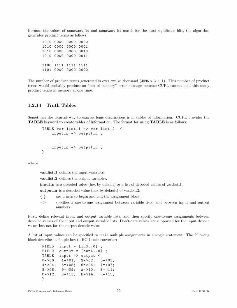
Because the values of constant_lo and constant_hi match for the least significant bits, the algorithmgenerates product terms as follows:
1010 0000 0000 0000
1010 0000 0000 0001
1010 0000 0000 0010
1010 0000 0000 0011
.
1100 1111 1111 1111
1101 0000 0000 0000
The number of product terms generated is over twelve thousand (4096 x 3 + 1). This number of productterms would probably produce an “out of memory” error message because CUPL cannot hold this manyproduct terms in memory at one time.
1.2.14 Truth Tables
Sometimes the clearest way to express logic descriptions is in tables of information. CUPL provides theTABLE keyword to create tables of information. The format for using TABLE is as follows:
TABLE var_list_1 => var_list_2 {
input_n => output_n ;
.
.
input_n => output_n ;
}
where
var list 1 defines the input variables.
var list 2 defines the output variables.
input n is a decoded value (hex by default) or a list of decoded values of var list 1.
output n is a decoded value (hex by default) of var list 2.
{ } are braces to begin and end the assignment block.
=> specifies a one-to-one assignment between variable lists, and between input and outputnumbers.
First, define relevant input and output variable lists, and then specify one-to-one assignments betweendecoded values of the input and output variable lists. Don’t-care values are supported for the input decodevalue, but not for the output decode value.
A list of input values can be specified to make multiple assignments in a single statement. The followingblock describes a simple hex-to-BCD code converter:
FIELD input = [in3 ..0] ;
FIELD output = [out4 ..0] ;
TABLE input => output {
0=>00; 1=>01; 2=>02; 3=>03;
4=>04; 5=>05; 6=>06; 7=>07;
8=>08; 9=>09; A=>10; B=>11;
C=>12; D=>13; E=>14; F=>15;
}
CUPL Programmer’s Reference Guide 55 Rev. 10/23/12

COMBINATORIALLOGIC STORAGE
REGISTERS
Non-Registered Outputs
Registered Outputs
State Bits
Inputs
Figure 1.18: State Machine Model
The following example illustrates the use of a list of input numbers to do address decoding for various-sizedRAM, ROM, and I/O devices. The address range is decoded according to the rules (in terms of indexedvariable usage) for the range operation (see Sec. 1.2.13, Range Operations).
PIN [1..4] = [a12 ..15] ; /* Upper 4 address */
PIN 12 = !RAM_sel ; /* 8K x 8 RAM */
PIN 13 = !ROM_sel ; /* 32K x 8 ROM */
PIN 14 = !timer_sel ; /* 8253 Timer */
FIELD address = [a15 ..12] ;
FIELD decodes = [RAM_sel ,ROM_sel ,timer_sel] ;
TABLE address => decodes {
[1000..2 FFF] => ’b’100; /* select RAM */
[5000.. CFFF] => ’b ’010; /* select ROM */
F000 => ’b ’001; /* select timer */
}
1.3 State-Machines
This section describes the CUPL state machine syntax, providing a brief overview of its use, a definition ofa state machine, and explaining in detail the CUPL state machine syntax.
The state-machine approach used with the CUPL compiler-based PLD language permits bypassing the gateand equation level stage in logic design and to move directly from a system-level description to a PLDimplementation. Additionally, unlike assembler-based approaches, the state-machine approach allows cleardocumentation of design, for future users.
1.3.1 State-Machine Model
A synchronous state machine is a logic circuit with flip-flops. Because its output can be fed back to its ownor some other flip-flop’s input, a flip-flop’s input value may depend on both its own output and that of otherflip-flops; consequently, its final output value depends on its own previous values, as well as those of otherflip-flops.
The CUPL state-machine model, as shown in Figure 1.18, uses six components: inputs, combinatorial logic,storage registers, state bits, registered outputs, and non-registered outputs.
The following definitions refer to the timing diagram in Figure 1.18.
CUPL Programmer’s Reference Guide 56 Rev. 10/23/12

TCO
CLOCK
TCO
T + TCO pd
T + TCO pd
Tpd
STATE BIT
REGISTERED OUTPUT
NON-REGISTERED OUTPUT(Depends only on state)
INPUT
NON-REGISTERED OUTPUT(Depends on state and input)
Figure 1.19: State MachineTiming Diagram
Inputs - are signals entering the device that originate in some other device.
Combinatorial Logic - is any combination of logic gates (usually AND-OR) that produces an outputsignal that is valid Tpd (propagation delay time) nsec after any of the signals that drive these gateschanges. Tpd is the delay between the initiation of an input or feedback event and the occurrence of anon-registered output.
State Bits - are storage register outputs that are fed back to drive the combinatorial logic. They containthe present-state information.
Storage Registers - are any flip-flop elements that receive their inputs from the state machine’s combi-natorial logic. Some registers are used for state bits: others are used for registered outputs. Theregistered output is valid Tco (clock to out time) nsec after the clock pulse occurs. Tco is the time delaybetween the initiation of a clock signal and the occurrence of a valid flip-flop output.
Figure 1.19 shows the timing relationships between the state machine components.
For the system to operate properly, the PLD’s requirements for setup and hold times must be met. For mostPLDs, the setup time (Tsu) usually includes both the propagation delay of the combinatorial logic and theactual setup time of the flip-flops. Tsu is the time it takes for the result of either feedback or an input eventto appear at the input to a flip-flop. A subsequent clock input cannot be applied until this result becomesvalid at the flip-flop’s input. The flip-flops can be either D, D-CE, J- K, S-R, or T types.
Non-registered Outputs - are outputs that come directly from the combinatorial logic gates. They maybe functions of the state bits and the input signals (and have asynchronous timing), or they may be purelydependent on the current state-bit values, in which case they become valid Tco + Tpd nsec after an activeclock edge occurs.
Registered Outputs - are outputs that come from the storage registers but are not included in the actualstate-bit field (that is, a bit field composed of all the state bits). State- machine theory requires that thesetting or resetting of these registered outputs depends on the transition from a present state to a next state.This allows a registered output to be either set or reset in a given state depending upon how the machinecame to be in that state. Thus, a registered output can assume a hold operation mode. In the hold mode,the registered output will remain at its last value as long as the current state transition does not specify anoperation on that registered output.
CUPL Programmer’s Reference Guide 57 Rev. 10/23/12

.Note: This hold mode of operation is available only for devices which use D-CE, J-K or S-R typeflip-flops.
1.3.2 State Machine Syntax
To implement the state machine model, CUPL supplies a syntax that allows the describing of any functionin the state machine.
The SEQUENCE keyword identifies the outputs of a state machine and is followed by statements thatdefine the function of the state machine. The format for the SEQUENCE syntax is as follows:
SEQUENCE state_var_list {
PRESENT state_n0 statements ;
.
.
.
PRESENT state_nn statements ;
}
where
state var list is a list of the state bit variables used in the state machine block. The variable listcan be represented by a field variable.
state n is the state number and is a decoded value of the state variable list and must be uniquefor each PRESENT statement.
statements are any of the conditional, next, or output statements described in the following sub-sections of this section.
; is a semicolon used to mark the end of a statement.
{ } are braces to mark the beginning and end of the state machine description.
Symbolic names defined with the $DEFINE command may be used to represent state numbers.
The SEQUENCE keyword causes the storage registers and registered output types generated to be thedefault type for the target device. For example, by using the SEQUENCE keyword in a design with aP16R8 target device, the state storage registers and registered outputs will be generated as D-type flip-flops.
The storage registers for certain devices can be programmed as more than one type. In the case of theF159 (Signetics PLS159), they can be either D or J-K type flip-flops. By default, using the SEQUENCEstatement with a design for the F159 will cause the state storage registers and registered outputs to begenerated as J-K type flip-flops. To override this default, the SEQUENCED keyword would be used inplace of the SEQUENCE keyword. This would cause the state registers and registered outputs to begenerated as D-type flip-flops.
Along with the SEQUENCE and SEQUENCED keywords are the SEQUENCEJK, SEQUENCERS,and SEQUENCET keywords. Respectively, they cause the state registers and registered outputs to begenerated as J-K, S-R, and T-type flip-flops.
The subsections that follow describe the types of statements that can be written in the state-machine syntax.Statements use the IF, NEXT, OUT and DEFAULT keywords.
CUPL Programmer’s Reference Guide 58 Rev. 10/23/12

Figure Missing
Figure 1.20: Unconditional NEXT Statement Diagram
Unconditional NEXT Statement
This statement describes the transition from the present state to a specified next state. The format is:
PRESENT state_n
NEXT state_n ;
where
state n is a decoded value of the state bit variables that are the output of the state machine.
A symbolic name can be assigned with the $DEFINE command to represent state n.
Because the statement is unconditional (that is, it describes the transition to a specific next state), therecan be only one NEXT statement for each PRESENT statement.
The following example specifies the transition from binary state 01 to binary state 10.
PRESENT ’b’01
NEXT ’b’10 ;
Figure 1.20 shows the transition described in the example above.
For the transition described in the example and figure above, CUPL generates the following equations,depending on the type of flip-flop that is specified:
D-Type Flip-Flop
APPEND Q1.D = !Q1 & Q0;
APPEND Q0.D = ’b’0; /* implicitly resets */
J-K-Type Flip-Flop
APPEND Q1.J = !Q1 & Q0;
APPEND Q1.K = ’b’0;
APPEND Q0.J = ’b’0;
APPEND Q0.K = !Q1 & Q0;
S-R-Type Flip-Flop
APPEND Q1.S = !Q1 & Q0;
APPEND Q1.R = ’b’0;
APPEND Q0.S = ’b’0;
APPEND Q0.R = !Q1 & Q0;
CUPL Programmer’s Reference Guide 59 Rev. 10/23/12

D-CE-Type Flip-Flop
APPEND Q1.D = !Q1 & Q0;
APPEND Q1.CE = !Q1 & Q0;
APPEND Q0.D = ’b’0;
APPEND Q0.CE = !Q1 & Q0;
T-Type Flip-Flop
APPEND Q1.T = !Q1 & Q0;
APPEND Q0.T = !Q1 & Q0;
See Sec. 1.2.9, APPEND Statements, for a description of the APPEND command.
Conditional NEXT Statement
This statement describes the transition from the present state to a next state if the conditions in a specifiedinput expression are met. The format is as follows.
PRESENT state_n
IF expr NEXT state_n;
.
.
.
IF expr NEXT state_n;
[DEFAULT NEXT state_n ;]
where
state n is a decoded value of the state bit variables that are the output of the state machine.
expr is any valid expression (see Sec. 1.2.8, Logic Expressions).
; is a semicolon used to mark the end of a statement.
.Note: The square brackets indicate optional items.
.Note: The value for each state number must be unique.
More than one conditional statement can be specified for each PRESENT statement.
The DEFAULT statement is optional. It describes the transition from the present state to a next stateif none of the conditions in the specified conditional statements are met. In other words, it describes thecondition that is the complement of the sum of all the conditional statements.
.Note: Be careful when using the DEFAULT statement. Because it is the complement of all theconditional statements, the DEFAULT statement can generate an expression complex enough to greatlyslow CUPL operation. In most applications, one or two conditional statements can be specified instead ofthe DEFAULT statement.
The following is an example of two conditional NEXT statements without a DEFAULT statement.
PRESENT ’b’01
CUPL Programmer’s Reference Guide 60 Rev. 10/23/12

Figure Missing
Figure 1.21: Conditional NEXT Statement Diagram
IF INA NEXT ’b’10;
IF !INA NEXT ’b’11;
Figure 1.21 shows the transitions described by the above example.
For the transitions described in the above example and figure, CUPL generates the following equations,depending on the type of flip-flop that is specified:
D-Type Flip-Flop
APPEND Q1.D = !Q1 & Q0;
APPEND Q0.D = !Q1 & Q0 & !INA;
D-CE-Type Flip-Flop
APPEND Q1.D = !Q1 & Q0;
APPEND Q1.CE = !Q1 & Q0;
APPEND Q0.D = !Q1 & Q0 & !INA;
APPEND Q0.CE = !Q1 & Q0 & INA;
J-K-Type Flip-Flop
APPEND Q1.J = !Q1 & Q0;
APPEND Q1.K = ’b’0;
APPEND Q0.J = ’b’0;
APPEND Q0.K = !Q1 & Q0 & INA;
S-R-Type Flip-Flop
APPEND Q1.S = !Q1 & Q0;
APPEND Q1.R = ’b’0;
APPEND Q0.S = ’b’0;
APPEND Q0.R = !Q1 & Q0 & INA;
T-Type Flip-Flop
APPEND Q1.T = !Q1 & Q0;
APPEND Q0.T = !Q1 & Q0 & INA;
The following is an example of two conditional statements with a DEFAULT statement.
PRESENT ’b’01
IF INA & INB NEXT ’b’10’;
CUPL Programmer’s Reference Guide 61 Rev. 10/23/12

Figure Missing
Figure 1.22: Conditional NEXT Statement with Default Diagram
IF INA & !INB NEXT ’b’11;
DEFAULT NEXT ’b’00;
Figure 1.22 shows the transitions described by the above example. Note the equation generated by theDEFAULT statement.
For the transitions described in the above example and figure, CUPL generates the following equations,depending on the type of flip-flop that is specified.
D-Type Flip-Flop
APPEND Q1.D = !Q1 & Q0 & INA;
APPEND Q0.D = !Q1 & Q0 & INA & !INB;
D-CE-Type Flip-Flop
APPEND Q1.D = !Q1 & Q0 & INA;
APPEND Q1.CE = !Q1 & Q0 & INA;
APPEND Q0.D = ’b’0;
APPEND Q0.CE = !Q1 & Q0 & !INA
# !Q1 & Q0 & INA & INB;
J-K-Type Flip-Flop
APPEND Q1.J = !Q1 & Q0 & INA;
APPEND Q1.K = ’b’0;
APPEND Q0.J = ’b’0;
APPEND Q0.K = !Q1 & Q0 & INA & INB
# !Q1 & Q0 & !INA;
S-R-Type Flip-Flop
APPEND Q1.S = !Q1 & Q0 & INA;
APPEND Q1.R = ’b’0;
APPEND Q0.S = ’b’0;
APPEND Q0.R = !Q1 & Q0 & INA & INB
# !Q1 & Q0 & !INA;
T-Type Flip-Flop
APPEND Q1.T = !Q1 & Q0 & INA;
APPEND Q0.T = !Q1 & Q0 & !INA
# !Q1 & Q0 & INA & INB;
CUPL Programmer’s Reference Guide 62 Rev. 10/23/12

Unconditional Synchronous Output Statement
This statement describes a transition from the present state to a next state, specifies a variable for theregistered (synchronous) outputs associated with the transition, and defines whether the variable is logicallyasserted. The format is as follows:
PRESENT state_n
NEXT state_n OUT [!] var ... OUT [!] var;
where
state n is a decoded value (default hex) of the state bit variables that are the output of the statemachine.
var is a variable name declared in the pin declarations. It is not a variable from the SEQUENCEstate var list.
! is the complement operator; use it to logically negate the variable, or omit it to logicallyassert the variable.
; is a semicolon used to mark the end of a statement.
.Note: The square brackets indicate optional items.
The PIN declaration statement (see Sec. 1.1.9, Pin Declaration Statements) determines whether the variable,when asserted, is active-HI or active-LO. For example, if the variable has the negation symbol (!var) in thepin declaration, when it is asserted in the OUT statement, its value is active-LO.
.Note: Use the negation mode only for D-CE, J-K, T or S-R type flip-flops; D-type flip-flops implicitlyreset when assertion is not specified.
The following is an example of an unconditional synchronous output statement.
PRESENT ’b’01
NEXT ’b’10 OUT Y OUT !Z ;
Figure 1.23 shows the transition and output variable definition described in the example above.
Figure Missing
Figure 1.23: Unconditional Synchronous Output Diagram
For the synchronous output definitions in the example and figure above, CUPL generates the followingequations, depending on the type of flip-flop that is specified.
D-Type Flip-Flop
APPEND Y.D = !Q1 & Q0;
(not defined for Z output)
CUPL Programmer’s Reference Guide 63 Rev. 10/23/12

D-CE Type Flip-Flop
APPEND Y.D = !Q1 & Q0;
APPEND Y.CE = !Q1 & Q0;
APPEND Z.D = ’b’0;
APPEND Z.CE = !Q1 & Q0;
J-K-Type Flip-Flop
APPEND Y.J = !Q1 & Q0;
APPEND Y.K = ’b’0;
APPEND Z.J = ’b’0;
APPEND Z.K = !Q1 & Q0;
S-R-Type Flip-Flop
APPEND Y.S = !Q1 & Q0;
APPEND Y.R = ’b’0;
APPEND Z.S = ’b’0;
APPEND Z.R = !Q1 & Q0;
T-Type Flip-Flop
APPEND Y.T = !Q1 & Q0;
APPEND Z.T = !Q1 & Q0;
Conditional Synchronous Output Statement
This statement describes a transition from the present state to a next state, specifies a variable for theregistered (synchronous) outputs associated with the transition, and defines whether the variable is logicallyasserted if the conditions specified in an input expression are met. The format is as follows:
PRESENT state_n
IF expr NEXT state_n OUT [!] var ... OUT [!] var;
.
.
IF expr NEXT state_n OUT [!] var ... OUT [!] var;
[[ DEFAULT] NEXT state_n OUT [!] var;]
where
state n is a decoded value (default hex) of the state bit variables that are the output of the statemachine.
var is a variable name declared in the pin declarations. It is not a variable from the SEQUENCEstate variable list.
! is the complement operator; use it to logically negate the variable, or omit it to logicallyassert the variable.
; is a semicolon used to mark the end of a statement.
expr is any valid expression.
.Note: The square brackets indicate optional items.
CUPL Programmer’s Reference Guide 64 Rev. 10/23/12

The PIN declaration statement (see Sec. 1.1.9, Pin Declaration Statements) determines whether the variable,when asserted, is active-HI or active-LO. For example, if the variable has the negation symbol (!var) in thepin declaration, when it is asserted in the OUT statement, its value is active-LO.
.Note: Use the negation mode only for J-K or S-R-type flip-flops; D-type flip-flops implicitly reset whenassertion is not specified.
The DEFAULT statement is optional. It describes the transition from the present state to a next state,and defines the output variable, if none of the conditions in the specified conditional statements are met. Inother words, it describes the condition that is the complement of the sum of all the conditional statements.
.Note: Be careful when using the DEFAULT statement. Because it is the complement of all theconditional statements, the DEFAULT statement can generate an expression complex enough to greatlyslow CUPL operation. In most applications, one or two conditional statements can be specified instead ofthe DEFAULT statement.
The following is an example of conditional synchronous output statements without a DEFAULT statement.
PRESENT ’b’01
IF INA NEXT ’b’10 OUT Y;
IF !INA NEXT ’b’11 OUT Z;
Figure 1.24 shows the transitions and outputs defined by the statements in the example above.
Figure Missing
Figure 1.24: Conditional Synchronous Output Diagram
For the synchronous output definitions in the example and figure above, CUPL generates the followingequations, depending on the type of flip-flop specified:
D-Type Flip-Flop
APPEND Y.D = !Q1 & Q0 & INA;
APPEND Z.D = !Q1 & Q0 & !INA;
D-CE-Type Flip-Flop
APPEND Y.D = !Q1 & Q0 & INA;
APPEND Y.CE = !Q1 & Q0 & INA;
APPEND Z.D = !Q1 & Q0 & !INA;
APPEND Z.CE = !Q1 & Q0 & !INA;
J-K-Type Flip-Flop
APPEND Y.J = !Q1 & Q0 & INA;
APPEND Y.K = ’b’0;
APPEND Z.J = !Q1 & Q0 & !INA;
CUPL Programmer’s Reference Guide 65 Rev. 10/23/12

APPEND Z.K = ’b’0;
S-R-Type Flip Flop
APPEND Y.S = !Q1 & Q0 & INA;
APPEND Y.R = ’b’0;
APPEND Z.S = !Q1 & Q0 & !INA;
APPEND Z.R = ’b’0;
T-Type Flip-Flop
APPEND Y.T = !Q1 & Q0 & INA;
APPEND Z.T = !Q1 & Q0 & !INA;
The following is an example of conditional output statements with a DEFAULT statement.
PRESENT ’b’01
IF INA & INB NEXT ’b’10;
IF INA & !INB NEXT ’b’11;
DEFAULT NEXT ’b’00 OUT Y
OUT !Z;
Figure 1.25 shows the transitions described by the above example. Note the equation generated by theDEFAULT statement.
Figure Missing
Figure 1.25: Conditional Synchronous Output with Default Diagram
For the transitions described in the above example and figure, CUPL generates the following equations,depending on the type of flip-flop that is specified.
D-Type Flip-Flop
APPEND Y.D = !Q1 & Q0 & !INA;
(not defined for Z output)
D-CE-Type Flip-Flop
APPEND Y.D = !Q1 & Q0 & !INA;
APPEND Y.CE = !Q1 & Q0 & !INA;
APPEND Z.D = ’b’0;
APPEND Z.CE = !Q1 & Q0 & INA;
J-K-Type Flip-Flop
APPEND Y.J = !Q1 & Q0 & !INA;
APPEND Y.K = ’b’0;
CUPL Programmer’s Reference Guide 66 Rev. 10/23/12

APPEND Z.J = ’b’0;
APPEND Z.K = !Q1 & Q0 & !INA;
S-R-Type Flip-Flop
APPEND Y.S = !Q1 & Q0 & !INA;
APPEND Y.R = ’b’0;
APPEND Z.S = ’b’0;
APPEND Z.R = !Q1 & Q0 & !INA;
T-Type Flip-Flop
APPEND Y.T = !Q1 & Q0 & !INA
APPEND Z.T = !Q1 & Q0 & INA;
Unconditional Asynchronous Output Statement
This statement specifies variables for the non-registered (asynchronous) outputs associated with a givenpresent state, and defines when the variable is logically asserted. The format is as follows:
PRESENT state_n
OUT var ... OUT var ;
where:
state n is a decoded value (default hex) of the state bit variables that are the output of the statemachine.
var is a variable name declared in the pin declarations. It is not a variable from the SE-QUENCE state var list.
; is a semicolon used to mark the end of a statement.
The PIN declaration statement (see Sec. 1.1.9, Pin Declaration Statements) determines whether the variable,when asserted, is active-HI or active-LO. For example, if the variable has the negation symbol (!var) in thepin declaration, when it is asserted in the OUT statement, its value is active-LO.
Negating the variable (with the complement operator) is not a valid format for this statement.
Only one output statement can be written for each present state. However, multiple variables can be definedusing more than one OUT keyword.
The following is an example of an unconditional asynchronous output statement.
PRESENT ’b’01
OUT Y OUT Z;
Figure 1.26 shows the outputs defined by the statements in the example above.
For the asynchronous output definitions in the example and figure above, CUPL generates the followingequations:
APPEND Y = !Q1 & Q0;
APPEND Z = !Q1 & Q0;
CUPL Programmer’s Reference Guide 67 Rev. 10/23/12

Figure Missing
Figure 1.26: Unconditional Asynchronous Output Diagram
Conditional Asynchronous Output Statement
This statement specifies variables for the non-registered (asynchronous) outputs associated with a givenpresent state, and defines when the variables are logically asserted, if the conditions in an input expressionare met. The format is as follows:
PRESENT state_n
IF expr OUT var ... OUT var;
.
.
IF expr OUT var ... OUT var;
[DEFAULT OUT var ... OUT var;]
where
state n is a decoded value (default hex) of the state bit variables that are the output of the statemachine.
var is a variable name declared in the pin declarations. It is not a variable from the SEQUENCEstatement.
expr is any valid expression.
; is a semicolon used to mark the end of a statement.
.Note: The square brackets indicate optional items.
The PIN declaration statement determines whether the variable, when asserted, is active-HI or active-LO.For example, if the variable has the negation symbol (!var) in the pin declaration, when it is asserted in theOUT statement, its value is active-LO.
Negating the variable (with the complement operator) is not a valid format for this statement. Multipleoutput statements can be written for each present state, and define multiple variables using the OUTkeyword.
The DEFAULT statement is optional. It defines the output variable if none of the conditions in the specifiedconditional statements are met. In other words, it describes the condition that is the complement of thesum of all the conditional statements.
.Note: Be careful when using the DEFAULT statement. Because it is the complement of all theconditional statements, the DEFAULT statement can generate an expression complex enough to greatlyslow CUPL operation. In most applications, one or two conditional statements can be specified instead ofthe DEFAULT statement.
CUPL Programmer’s Reference Guide 68 Rev. 10/23/12

The following is an example of conditional asynchronous output statements without a default statement.
PRESENT ’b’01
IF INA OUT Y;
IF !INA OUT Z;
Figure 1.27 shows the outputs defined by the statements in the above example.
Figure Missing
Figure 1.27: Conditional Asynchronous Output Diagram
For the asynchronous output definitions in the example and figure above, CUPL generates the followingequations:
APPEND Y = !Q1 & Q0 & INA;
APPEND Z = !Q1 & Q0 & !INA;
The following is an example of conditional asynchronous output statements with a DEFAULT statement.
PRESENT ’b’01
IF INA & INB OUT X;
IF INA & !INB OUT Y;
DEFAULT OUT Z;
Figure 1.28 shows the transitions described by the above example. Note the equation generated by theDEFAULT statement.
Figure Missing
Figure 1.28: Conditional Asynchronous Output with Default Diagram
For the transitions described in the above example and figure, CUPL generates the following equations,depending on the type of flip-flop that is specified.
APPEND X = !Q1 & Q0 & INA & !INB;
APPEND Y = !Q1 & Q0 & INA & INB;
APPEND Z = !Q1 & Q0 & !INA;
Sample State-Machine Syntax File
This section provides an example of a simple two-bit counter implemented with state-machine syntax.
CUPL Programmer’s Reference Guide 69 Rev. 10/23/12

Figure 1.29 shows a diagram of the counter operation.
Figure Missing
Figure 1.29: Simple 2-Bit Counter Diagram
The $DEFINE command assigns symbolic names to the states of the counter, and the SEQUENCE state-ment defines the transitions between states.
$DEFINE S0 0 /* assign symbolic names */
$DEFINE S1 1 /* to states */
$DEFINE S2 2
$DEFINE S3 3
FIELD count = [Q1, Q0];
/* assign field variable to statebits */
SEQUENCE count {
PRESENT S0 NEXT S1 ;
PRESENT S1 NEXT S2 ;
PRESENT S2 NEXT S3 ;
PRESENT S3 NEXT S0 ;
}
See the example, Decade Up/Down Counter, in Chapter U5 for another illustration of a state machineimplementation.
1.3.3 Condition Syntax
The CONDITION syntax provides a higher-level approach to specifying logic functions than does writingstandard Boolean logic equations for combinatorial logic. The format is as follows:
CONDITION {
IF expr0 OUT var ;
.
.
IF exprn OUT var ;
DEFAULT OUT var ;
}
where
expr is any valid expression.
var is a variable name declared in the pin declaration. It can also be a list of indexed ornon-indexed variables in list notation.
; is a semicolon used to mark the end of a statement.
CUPL Programmer’s Reference Guide 70 Rev. 10/23/12

The CONDITION syntax is equivalent to the asynchronous conditional output statements of the statemachine syntax, except that there is no reference to any particular state. The variable is logically assertedwhenever the expression or DEFAULT condition is met.
The variable cannot be logically negated in this format.
.Note: Be careful when using the DEFAULT statement. Because it is the complement of all theconditional statements, the DEFAULT statement can generate an expression complex enough to greatlyslow CUPL operation. In most applications, one or two conditional statements may be specified instead ofthe DEFAULT statement.
The following is an example of a 2 to 4 line decoder for the CONDITION syntax. The two data inputs, Aand B, select one of four decoded outputs, Y0 through Y3, whenever the ENABLE signal is asserted. TheNO MATCH output is asserted if none of the other four outputs are true.
PIN [1,2] = [A,B] ; /* Data Inputs */
PIN 3 = !enable ; /* Enable Input */
PIN [12..15] = [Y0..3] ; /* Decoded Outputs */
PIN 14 = no_match ; /* Match Output */
CONDITION {
IF enable & !B & !A out Y0 ;
IF enable & !B & A out Y1 ;
IF enable & B & !A out Y2 ;
IF enable & B & A out Y3 ;
}
The DEFAULT expression of the above example is equivalent to the following logic equation
no_match = !( enable & !B & !A)
# enable & !B & A
# enable & B & !A
# enable & B & A ;
which reduces to the following:
no_match = !enable ;
1.3.4 User-Defined Functions
The FUNCTION keyword permits the creating of personal keywords by encapsulating some logic as afunction and giving it a name. This name can then be used in a logic equation to represent the function.The format for user-defined functions is as follows:
FUNCTION name ([parameter0 ,.... , parametern ])
{ body }
where
name is any group of valid symbols used to reference the function. Do not use any of the CUPLreserved keywords.
parameter is an optional variable used to reference variables when the function is used in a logicequation. It cannot be an expression.
CUPL Programmer’s Reference Guide 71 Rev. 10/23/12

body is any combination of logic equations, truth tables, state-machine syntax, condition syntax,or user function.
( ) are parentheses used to enclose the parameter list.
{ } are braces used to enclose the body of the function.
.Note: The square brackets indicate optional items.
The statements in the body may assign an expression to the function, or may be unrelated equations.
When using optional parameters, the number of parameters in the function definition and in the referencemust be identical. The parameters defined in the body of the function are substituted for the parametersreferenced in the logic equation.
For example, the following defines an exclusive OR function:
FUNCTION xor(in1 , in2) {
/* in1 and in2 are parameters */
xor = in1 & in2 # !in1 & in2 ;
}
An xor can be used in an equation with the inputs A and B passed as parameters, as follows:
Y = xor(A,B) ;
The result is the following logic equation assignment for the output variable Y:
Y = A & !B # !A & B ;
When a function variable is referenced in an expression, the compiler takes the following action:
1. A special function invocation variable is assigned for the function name and its arguments. Thisvariable name is not user accessible.
2. The rest of the expression is evaluated.
3. The function body, with the invocation parameters substituted, is evaluated.
4. The function invocation variable is assigned an expression according to the body of the function. If noassignment is made in the body statements, the function invocation variable is assigned the value of’h’0.
.Note: Functions must be defined before they may be referenced. Functions are not recursive; that is, afunction body may not include a reference of the function being defined.
The following example shows a user-defined function to construct state-machine-type transitions for non-registered devices without internal feedback (such as PROMs).
FUNCTION TRANSITION(present_state ,
next_state ,
input_conditions ) {
APPEND state_out = state_in:present_state &
input_condition &
next_state;
}
CUPL Programmer’s Reference Guide 72 Rev. 10/23/12

The function defined in the example above is used in the following example to implement a simple up/downcounter as a series of TRANSITION function references:
PIN [10 ,11] = [Qin0 ..1]; /* Registered PROM */
/* output feed back externally on input pins*/
PIN [12 ,13] = [count0 ..1] ; /* Count Control */
PIN [1,2] = [Q0..1] ; /* PROM Outputs */
FIELD state_in = [Qin0 ..1] ;
FIELD state_out = [Q0..1] ;
count_up = !count1 & !count0 ; /* count up */
count_dn = !count1 & count0 ; /* count down */
hold_cnt = count1; /* hold count */
$DEFINE STATE0 ’b’00
$DEFINE STATE1 ’b’01
$DEFINE STATE2 ’b’10
$DEFINE STATE3 ’b’11
/* (transition function definition made here) */
TRANSITION(STATE0 , STATE1 , count_up) ;
TRANSITION(STATE1 , STATE2 , count_up) ;
TRANSITION(STATE2 , STATE3 , count_up) ;
TRANSITION(STATE3 , STATE0 , count_up) ;
TRANSITION(STATE0 , STATE3 , count_dn) ;
TRANSITION(STATE1 , STATE0 , count_dn) ;
TRANSITION(STATE2 , STATE1 , count_dn) ;
TRANSITION(STATE3 , STATE2 , count_dn) ;
TRANSITION(STATE0 , STATE0 , hold_cnt) ;
TRANSITION(STATE1 , STATE1 , hold_cnt) ;
TRANSITION(STATE2 , STATE2 , hold_cnt) ;
TRANSITION(STATE3 , STATE3 , hold_cnt) ;
1.4 Input Files
A logic description source file (filename.PLD) is the input to CUPL. This file describes the logical function-ality to assign to a specified target device.
The source file is created using a standard text editor. There are a wide variety of text editors available andthe choice depends entirely upon personal preference. The only requirement is that it be able to produce astandard text file.
CUPL Programmer’s Reference Guide 73 Rev. 10/23/12

Chapter 2
Simulator Reference
This chapter explains how to use CSIM program to create test vectors for the programmable logic deviceunder design. Test vectors specify the expected functional operation of a PLD by defining the outputs as afunction of the inputs. Test vectors are used both for simulation of the device logic before programming andfor functional testing of the device once it has been programmed. CSIM can generate JEDEC-compatibledownloadable test vectors.
2.1 Input
A test specification source file (filename.SI) is the input to CSIM. It contains a functional description ofthe requirements of the device in the circuit.
The source file may be created using a standard text editor like DOS EDLIN or WordStar in non-documentmode.
The input pin stimuli and output pin test values entered in the source file are compared to the actual valuescalculated from the logic equations in the CUPL source file. These calculated values are contained in theabsolute file (filename.ABS), which is created during CUPL operation when the -a flag on the commandline is specified. The absolute file must be created during CUPL operation before running CSIM.
CSIM must also be able to access the device library file, CUPL.DL, which contains a description of each ofthe target devices supported in the current version of CSIM.
The library describes the physical characteristics of each device, including internal architecture, number ofpins, and type of registers available, and the logical characteristics, including registered and non-registeredpins, feedback capabilities, register power-on state and register control features.
Reference the target device using device mnemonics. Each mnemonic is composed of a device family prefixand industry-standard part number suffix. Table 2.1 lists the device mnemonic prefixes.
For example, the device mnemonic for a PAL10L8 is P10L8; for an 82S100 the device mnemonic is F100.For bipolar PROMs, the suffix is the array size. For example, the device mnemonic for a 1024 x 8 bipolarPROM is RA10P8, since there are 10 address input pins and 8 data output pins.
74

Prefix Device FamilyEP Erasable Programmable Logic Device (EPLD)G Generic Array Logic (GAL)F Field Programmable Logic Array (FPLA)F Field Programmable Gate Array (FPGA)F Field Programmable Logic Sequencer (FPLS)F Field Programmable Sequence Generator (FPSG)P Programmable Logic Array (PAL)P Programmable Logic Device (PLD)P Programmable Electrically Erasable Logic (PEEL)PLD Pseudo Logical DeviceRA Bipolar Programmable Read-Only Memory (PROM)
Table 2.1: CSIM Device Mnemonic Prefixes
2.2 Output
The simulator output is the following two files: a simulation listing file and an optional JEDEC downloadablefuse link file.
A simulation listing file (filename.SO) contains the results of the simulation. It has the same filename asthe input test specification file.
All header information is displayed in the listing file with any header errors marked appropriately. Eachcomplete vector is assigned a number. Any output tests that failed are flagged with the actual (simulator-determined) output value displayed. Each variable in error is listed along with the expected (user-supplied)value. Any invalid or unexpected test values are listed along with an appropriate error message.
The simulator output listing can also be output to the screen (using the -v option on the command line).
An optional JEDEC downloadable fuse link file (filename.JED) contains structured test vectors. CSIMappends the test vectors to an existing filename.JED created during CUPL operation.
.Note: CSIM does not support multi-device files as does CUPL. CSIM only simulates the first deviceof a multi-device file.
2.3 Virtual Simulation
Virtual simulation allows you to create a design without a target device and simulate it. It is possible,therefore, to get a working design before deciding what architecture it will be targeted to. This will beespecially useful for designs that will be eventually partitioned.
Usage of the virtual simulator is transparent. When you simulate any design, CSIM will examine whatthe device is and simulate the design accordingly. You do not need to learn any new commands or syntax.Just use the VIRTUAL device mnemonic when compiling and simulating to take advantage of the Virtualsimulator.
Virtual simuation is also used to simulate FPGA designs. When a full architectural simulation is not possibledue to the proprietary nature of the device internals or the level of complexity of the internal logic resources,
CUPL Programmer’s Reference Guide 75 Rev. 10/23/12

PARTNO NAMEREVISION DATEDESIGNER COMPANYASSEMBLY LOCATIONDEVICE FORMAT
Table 2.2: CSIM Header Keywords
Virtual simulation is the next best alternative for your design verification phase.
2.4 Header Information
Header information which is entered must be identical to the information in the corresponding CUPL logicdescription file. If any header information is different, a warning message appears, stating that the status ofthe logic equations could be inconsistent with the current test vectors in the test specification file. Table 2.2lists the keywords used for header information (see Sec. 1.1.8, Header Information):
When creating a test specification file, begin by copying the contents of the corresponding CUPL source fileto the test specification file, to assure proper header information. Then delete everything except the headerinformation from the test specification file.
2.5 Comments
Comments can be placed anywhere within the test specification file. Comments can be used to explainthe contents of the specification file or the function of certain test vectors. A comment begins with a slash-asterisk (/*) and ends with an asterisk-slash (*/). Comments can span multiple lines and are not terminatedby the end of a line. However, comments cannot be nested.
2.6 Statements
CSIM provides the keywords, ORDER, BASE, and VECTORS to write statements in the source filethat determine the simulation output and how it is displayed. The following sections describe how to writestatements with the CUPL keywords.
2.6.1 ORDER Statement
Use the ORDER keyword to list the variables to be used in the simulation table, and to define how they aredisplayed. Typically, the variable names are the same as those in the corresponding CUPL logic descriptionfile.
Place a colon after ORDER, separate each variable in the list with a comma, and terminate the list witha semicolon. The following is an example of an ORDER statement:
ORDER: inputA , inputB , output ;
CUPL Programmer’s Reference Guide 76 Rev. 10/23/12

Only those variables that are actually used in the simulation must be listed.
The polarity of the variable name can be different than was declared in the CUPL logic description file,allowing simulation of active-LO outputs with an active-HI simulation vector. The variable names can beentered in any order; CSIM automatically creates the proper order and polarity of the resulting vector tomatch the requirements of the JEDEC download format for the device.
When indexed variables are used in the ORDER statement, they can be expressed in list notation format.However, since the ORDER statement is already in list form, square brackets are not needed to delimit theORDER set. The following is an example of two equivalent ORDER statements; the first statement listsall the variables, and the second is written in list form.
ORDER: A0 , A1 , A2, A3, SELECT , !OUT0 , !OUT1;
ORDER: A0..3, SELECT , !OUT0 ..1 ;
In list notation format, the polarity of the first indexed variable (!OUT0 in the above example) determinesthe polarity for the entire list.
Bit fields that are declared in the CUPL logic description file can be referenced by their single variablename. Bit fields can also be declared in the test specification file for CSIM, using FIELD declarationstatements (see Bit Field Declaration Statements in Chapter 2). The FIELD statement must appear beforethe ORDER statement.
The ORDER statement can be used to specify the format of the vector results in the simulator listing file(or on the screen if screen output is specified.) By default, variable values are displayed without spacesbetween columns. For example, the following ORDER statement
ORDER: clock , input , output ;
generates the following display in the output file (using sample values):
0001: C0H
0002: C1L
Spaces can be inserted between columns by using the % symbol and a decimal value between 1 and 80. Forexample, the following ORDER statement
ORDER: clock , %2, input , %2, output ;
generates the following display in the output file:
0001: C 0 H
0002: C 1 L
.Note: The ORDER statement must be terminated by a semicolon.
Text can be inserted into the output file by putting a character string, enclosed by double quotes (” ”,) intothe ORDER statement. (Do not place text in the ORDER statement if waveform output will be used.)For example, the following ORDER statement
ORDER: "Clock is ", clock ,
" and input is ", input ,
" output goes ", output ;
produces the following result in the output file:
CUPL Programmer’s Reference Guide 77 Rev. 10/23/12

0001: Clock is C and input is 0 output goes H
0002: Clock is C and input is 1 output goes L
2.6.2 BASE Statement
In most cases, each variable in the ORDER statement (except for FIELD variables) has a correspondingsingle character test value that appears in the test vector table of the output file. Multiple test vector valuescan be represented with quoted numbers. Use single quotes for input values and double quotes for outputvalues. Enter a BASE statement to specify how each quoted number is expanded. The format for the BASEstatement is:
BASE: name;
where name is either octal, decimal or hex. Follow BASE with a colon.
.Note: The base statement must be terminated by a semicolon.
The default base for quoted test values is hexadecimal. The BASE statement must appear in the file beforethe ORDER statement.
If the base is decimal or hexadecimal, quoted numbers expand to four digits; if the base is octal, they expandto three digits. For example, a test vector entered as ’7’ is interpreted as follows:
1 1 1 Base is octal
or
0 1 1 1 Base is decimal
or
0 1 1 1 Base is hex
More than one hexadecimal or octal digit may be entered between quotes. For example, ’563’ expands tothe following:
1 0 1 1 1 0 0 1 1 Base is octal
or
0 1 0 1 0 1 1 0 0 0 1 1 Base is decimal
or
0 1 0 1 0 1 1 0 0 0 1 1 Base is hex
Quoted values may also be used with all other test values. For example, if the base is set to octal
"XX" expands to X X X X X X
"LL" expands to L L L L L L
"45" expands to H L L H L H
CUPL Programmer’s Reference Guide 78 Rev. 10/23/12

Test Value Description0 Drive input LO (0 volts) (negate active-HI input)1 Drive input HI (+5 volts) (assert active-HI input)C Drive (clock) input LO, HI, LOK Drive (clock) input HI, LO, HIL Test output LO (0 volts) (active-HI output negated)H Test output HI (+5 volts) (active-HI output asserted)Z Test output for high impedanceX Input HI or LO, output HI or LO.
Note: Not all device programmers treat X on inputs the same;some put it to 0, some allow input to be pulled to 1, and someleave it at the previous value.
N Output not testedP Preload internal registers (value is applied to !Q output)* Outputs only -simulator determines test value and substitutes in
vector’ ’ Enclose input values to be expanded to a specified BASE (octal,
decimal, or hex). Valid values are 0-F and X." " Enclose output values to be expanded to a specified BASE (octal,
decimal, or hex.) Valid values are 0-F, H, L, Z, and X.
Table 2.3: Test Vector Values
.Note: Quoted values cannot contain *.
Test values for FIELD variables can be expressed either individually (for example, 001, HHLL) or with quotedvalues (for example, ’1’, "C"). When quoted values are used, the value is automatically expanded to thenumber of variables in the field. For example, for the following address field
FIELD address = [A0..5] ;
A test value of
A A A A A A
5 4 3 2 1 0
------------------
1 1 1 0 0 1
could be written using single test values, or ’39’ using quoted test values.
2.6.3 VECTORS Statement
Use the VECTORS keyword to prefix the test vector table. Following the keyword, include test vectorsmade up of single test values or quoted test values (see Sec. 2.6.2, Base Statement). Each vector must becontained on a single line. No semicolons follow the vector. Table 2.3 lists allowable test vector values.
The following is an example of a test vector table:
VECTORS:
0 0 1 1 1 ’F’ Z "H" /* test outputs HI */
0 1 1 0 0 ’0’ Z "L" /* test outputs LO */
CUPL Programmer’s Reference Guide 79 Rev. 10/23/12

NOT : ones complement !
0 11 0X X
A !A
AND &
0 0 L0 1 L0 X L1 0 L1 1 H1 X XX X X
A B A & B
OR #
0 0 L0 1 H0 X X1 0 H1 1 H1 X HX X X
A B A # B
XOR : exclusive OR $
0 0 L0 1 H0 X X1 0 H1 1 L1 X XX X X
A B A $ B
Figure 2.1: Vector Truth Tables
Unlike many other simulators, CSIM treats the DON’T-CARE (state X) as any other value. State X is notassumed to be 0 on input and N on the output. The X state allows specific determination of which inputsaffect the output value, according to the rules listed in the truth tables in Table 2.1.
Preload
Use the P test value on the clock pin of a registered device to preload internal registers of a state machine orcounter design to a known state, if the device does not have a dedicated TTL-level preload pin. The deviceprogrammer uses a supervoltage to actually load the registers. All input pins to the device are ignored andhence should be defined as X. The values that appear for registered variables are loaded into the !Q outputof the register. These values (0 or 1) are absolute levels and are not affected by output polarity nor invertingbuffers. The following is an example of a preload sequence for an active-LO output variable in a device withan inverting buffer between the register Q output and device pin:
ORDER: clock , input1 , input2 , !output ;
VECTORS:
P X X 1 /* reset flip -flop */
/* !Q goes to 1 */
/* Q goes to 0 */
0 X X H /* output is HI due to */
/* inverting buffer */
CUPL Programmer’s Reference Guide 80 Rev. 10/23/12

Figure Missing
Figure 2.2: Circuit with Feedback
.Note: CSIM can simulate and preload test vectors even for devices that do not have preload capability.However, not all PLDs are capable of preload using a supervoltage. Some devices have dedicated preloadpins to use for this purpose. CSIM does not verify whether the device under simulation is actually capable ofpreload because parts from different manufacturers exhibit different characteristics. Before using the preloadcapability, determine whether the device being tested is physically capable of supervoltage preloading.
Clocks
Most synchronous devices (devices containing registers with a common clock tied to an output pin) use anactive-HI (positive edge triggered) clock. To assure proper CSIM operation for these devices, always usea C test value (not a 1 or 0) on the clock pin. For synchronous devices with an active-LO (negative edgetriggered) clock, use the K test value on the clock pin.
Asynchronous Vectors
When writing test vectors for a circuit with asynchronous feedback, changing two test values at once cancreate a spike condition that produces anomalous results. (See Figure 2.2. It shows the diagram for a circuitwith three inputs [A, B, and C] and an output at Y that feeds back.)
The equation for the output at Y is as follows:
Y = A & B & C # C & Y
The vectors below show an expected low output at Y based on the specified input values.
A B C Y
0001 0 0 0 L
0002 0 1 1 L
0003 1 0 1 L
Because one of the inputs is 0 in each of the vectors, the AND gate defined by A, B, and C produces a lowoutput. The low value feeding back from the Y output keeps the other AND gate low also. Therefore, theOR gate (driven by the output of the two AND gates) and consequently the output at Y remain low for thespecified test vectors.
However, when the programmer operates on the test vectors, it applies values serially, beginning with thefirst pin. Because two test values change between vectors, the programmer creates intermediate results(labeled “a” below).
CUPL Programmer’s Reference Guide 81 Rev. 10/23/12

ARRAY
Y
A
B
MACROCELL
Figure 2.3: I/O Pin Simulation
A B C Y
0001 0 0 0 L
0001a 0 1 0 L
0002 0 1 1 L
0002a 1 1 1 H
0003 1 0 1 H
The intermediate result, [0002a], produces a high value for the output at Y. This high value feeds back andcombines with the “1” value specified for input C in vector [0003] to produce a high output for the ANDgate and consequently for the OR gate and for the output at Y. This high value conflicts with the expectedlow value specified in the third test vector, and the result is a spike condition.
By taking care to always change only one value between test vectors, the spike condition described abovecan be avoided. Also, in the source specification file, it is possible to specify a TRACE value of 1, 2, or 3(rather than the default value of 0) that instructs CSIM to display intermediate results in the output file(see “TRACE” in the following section, Simulator Directives).
I/O Pin simulation
When writing test vectors for a design that has input/output capability and a controllable output enable(OE), the test vector value placed at the I/O pin will depend on the value of the output enable. If the outputenable is active, the I/O pin needs an output test value (L, H, *,...). If the output enable becomes inactive,a Hi-Z (Z) will appear on the I/O pin. At this time, input test values (0, 1, ...) can be placed on the I/Opin allowing that pin to behave as an input pin. When the output enable is activated again, the test valuesfor that pin will reflect the output of the macrocell.
The following equations express the boolean equation representation of Figure 2.3:
Y = B;
Y.OE = A;
When A is TRUE, the output of the macrocell (B) will appear at the pin (Y). When A is FALSE, the outputenable will be deactivated and a Hi-Z will appear at the pin (Y). After the output enable is deactivated,input values can be placed on the pin. Here is an example of what the simulation file will look like:
Order: A, %1, B, %3, Y;
CUPL Programmer’s Reference Guide 82 Rev. 10/23/12

Vectors:
1 0 L /* OE is ON */
1 1 H
0 0 Z /* OE is OFF */
0 0 1 /* a valid input value can be placed on pin Y */
1 0 L /* OE is ON again */
Multiple ORDER statements
CSIM allows several ORDER statements to be defined in a single SI file. For example, if the file TEST.SI
has the following contents:
Name test;
Partno XXXXX;
Date XX/XX/XX;
Revision XX;
Designer XXXXX;
Company XXXXX;
Assembly XXXXX;
Location XXXXX;
Device g16v8;
Order: A, %1, B, %1, X, %1, Y;
Vectors:
0 0 H L
0 1 H H
1 0 H H
1 1 L L
0 X H X
X 0 H X
1 X X X
X 1 X X
Order: A, B, X;
Vectors:
0 0 H
0 1 H
1 0 H
1 1 L
0 X H
X 0 H
1 X X
X 1 X
The file TEST.SO will look like this:
CSIM: CUPL Simulation Program
Version 4.2a Serial# ...
Copyright (c) 1983, 1991 Logical Devices , Inc.
CREATED Wed Dec 04 02:14:12 1991
LISTING FOR SIMULATION FILE: test.si
1: Name test;
2: Partno XXXXX;
CUPL Programmer’s Reference Guide 83 Rev. 10/23/12

3: Date XX/XX/XX;
4: Revision XX;
5: Designer XXXXX;
6: Company XXXXX;
7: Assembly XXXXX;
8: Location XXXXX;
9: Device g16v8;
10:
11: Order: A, %1, B, %1, X, %1, Y;
12:
================
A B X Y
================
0001: 0 0 H L
0002: 0 1 H H
0003: 1 0 H H
0004: 1 1 L L
0005: 0 X H X
0006: X 0 H X
0007: 1 X X X
0008: X 1 X X
25: Order: A, B, X; 26:
============
ABX
============
0010: 00H
0011: 01H
0012: 10H
0013: 11L
0014: 0XH
0015: X0H
0016: 1XX
0017: X1X
Random Input Generation
A new test vector value is now supported:
R - it can appear wherever a 0 or a 1 can appear. When encountering such a value, CSIMgenerates a random value ( that is 0 or 1) for the corresponding signal in that test vector.
.Note: R can only be used to generate random input values
In the SI file:
$repeat 10;
C 0 RRR 1RRRRRRR ********
In the SO file:
0035: C 0 000 10001011 HLLLHLHH
CUPL Programmer’s Reference Guide 84 Rev. 10/23/12

0036: C 0 000 11100111 HHHLLHHH
0037: C 0 110 10111101 HHHHLHHL
0038: C 0 111 11000100 HLLLHLLH
0039: C 0 101 10001011 LHLHHHLL
0040: C 0 101 10000110 LLHHLHLL
0041: C 0 010 10000001 LHHLLLLL
0042: C 0 000 10010000 HLLHLLLL
0043: C 0 001 11110100 LHHHHLHL
0044: C 0 001 10011110 LHLLHHHH
2.7 Simulator Directives
CSIM provides six directives that can be placed on any row of the file after the VECTOR statement. Alldirective names begin with a dollar sign and each directive statement must end with a semicolon. Table 2.4lists the CSIM directives.
$MSG $REPEAT $TRACE
$SIMOFF $SIMON $EXIT
Table 2.4: CSIM Directives
2.7.1 $MSG
Use the $MSG directive to place documentation messages or formatting information into the simulatoroutput file. For example, a header for the simulator function table, listing the variable names, may becreated. The format is as follows:
$MSG "any text string" ;
In the output table, the text string appears without the double quotes.
Blank lines can be inserted into the output, for example, between vectors, by using the following format:
$MSG "" ;
The $MSG directive can be also used to place markers in the simulator output file. The markers will bedisplayed on the screen at display waveform time (if the “w” flag was set). To mark a vector, place thefollowing statement on the line preceding the vector to be marked:
$MSG "mark"
2.7.2 $REPEAT
The $REPEAT directive causes a vector to be repeated a specified number of times. Its format is:
$REPEAT n ;
where
CUPL Programmer’s Reference Guide 85 Rev. 10/23/12

n is a decimal value between 1 and 9999.
The vector following the $REPEAT directive is repeated the specified number of times.
The $REPEAT directive is particularly useful for testing counters and state transitions. Use the asterisk(*) to represent output test values supplied by CSIM. The following example shows a a 2-bit counter froma CUPL source file, and a VECTORS statement using the $REPEAT directive to test it.
From CUPL:
Q0.d = !Q0 ;
Q1.d = !Q1 & Q0 # Q1 & !Q0 ;
In CSIM:
ORDER: clock , input , Q1, Q0 ;
VECTORS:
0 0 X X /* power -on condition */
P X 1 1 /* reset the flip -flops */
0 0 H H
$REPEAT 4 ; /* clock 4 times */
C 0 * *
The above file generates the following test vectors:
0 0 X X
P X 1 1
0 0 H H
C 0 L L
C 0 L H
C 0 H L
C 0 H H
CSIM supplies four sets of vector values.
2.7.3 $TRACE
Use the $TRACE directive to set the amount of information that CSIM prints for the vectors duringsimulation. The format is
$TRACE n ;
where
n is a decimal value between 0 and 4.
Trace level 0 (the default) turns off any additional information and only the resulting test vectors areprinted.
When non-registered feedback is used in a design, the value for the output feeding back is unknown forthe first evaluation pass of the vector. If the new feedback value changes any output value, the vector isevaluated again. All outputs must be identical for two passes before the vector is determined to be stable.
CUPL Programmer’s Reference Guide 86 Rev. 10/23/12

Trace level 1 prints the intermediate results for any vector that requires more than one evaluation pass tobecome stable. Any vector that requires more than twenty evaluation passes is considered unstable.
Trace level 2 identifies three phases of simulation for designs using registers. The first phase is “Before theClock,” where intermediate vectors using non-registered feedback are resolved. The second phase is “At theClock,” where the values of the registers are given immediately after the clock. The third phase is “Afterthe Clock,” where the outputs utilizing feedback are resolved as in trace level 1.
Trace level 3 provides the highest level of display information possible from CSIM. Each simulation phase of“Before Clock,” “At Clock,” and “After Clock” is printed and the individual product term for each variableis listed. The output value for the AND gate is listed along with the value of the inputs to the AND array.
Trace level 4 provides the ability to watch the logical value before the output buffer. Using $TRACE 4, CSIMonly reports the true output pin values, and assigns a “?” to inputs and buried nodes. For combinatorialoutput, trace level 4 displays the results of the OR term. For registered outputs, trace level 4 shows the Qoutput of the register.
The following example uses a p22v10:
pin 1 = CLK;
pin 2 = IN2;
pin 3 = IN3;
....
pin 14 = OUT14;
pin 15 = OUT15;
....
OUT 14.D = IN2;
OUT 14.AR = IN3;
OUT 14.OE = IN4;
....
The following shows the simulation result file:
order CLK , IN2 , IN3 , IN4 , . OUT14 , OUT15 . ;
****** before output buffer ******
???? .. LL ...
0001:0011 .. HH ...
.....
****** before output buffer ******
???? HH...
0004 C100 ...ZZ
.....
Figure 2.4 shows the virtual observation points when using trace level 4 with either a combinatorial config-uration or a register configuration.
2.7.4 $EXIT
Use the $EXIT directive to abort the simulation at any point. Test vectors appearing after the $EXITdirective are ignored. This directive is useful in debugging registered designs in which a false transition inone vector causes an error in every vector thereafter.
CUPL Programmer’s Reference Guide 87 Rev. 10/23/12
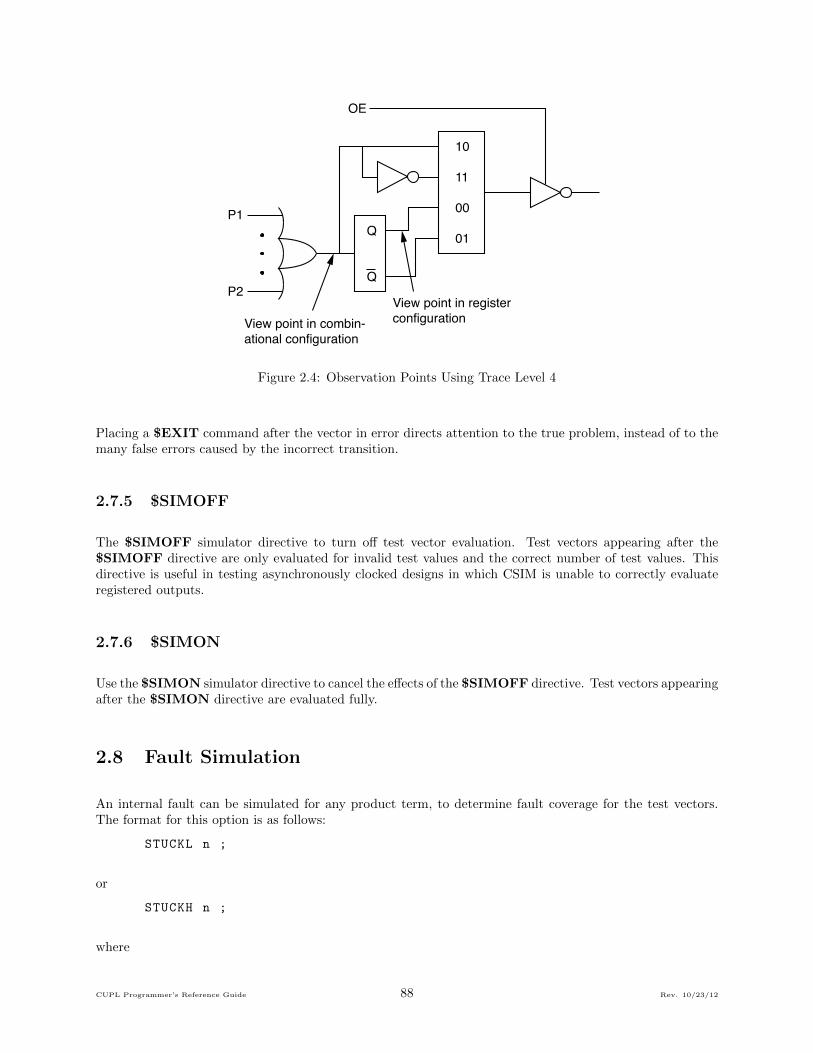
10
11
00
01Q
Q
OE
P1
P2View point in registerconfiguration View point in combin-
ational configuration
Figure 2.4: Observation Points Using Trace Level 4
Placing a $EXIT command after the vector in error directs attention to the true problem, instead of to themany false errors caused by the incorrect transition.
2.7.5 $SIMOFF
The $SIMOFF simulator directive to turn off test vector evaluation. Test vectors appearing after the$SIMOFF directive are only evaluated for invalid test values and the correct number of test values. Thisdirective is useful in testing asynchronously clocked designs in which CSIM is unable to correctly evaluateregistered outputs.
2.7.6 $SIMON
Use the $SIMON simulator directive to cancel the effects of the $SIMOFF directive. Test vectors appearingafter the $SIMON directive are evaluated fully.
2.8 Fault Simulation
An internal fault can be simulated for any product term, to determine fault coverage for the test vectors.The format for this option is as follows:
STUCKL n ;
or
STUCKH n ;
where
CUPL Programmer’s Reference Guide 88 Rev. 10/23/12

n is the JEDEC fuse number for the first fuse in the product term.
The documentation file (filename.DOC) fuse map lists the fuse numbers for the first fuse in each productterm in the device.
Format 1 forces the product term to be stuck-at-0.
Format 2 forces the product term to be stuck-at-1. The STUCK command must be placed between theORDER and VECTORS statements.
2.9 Additional Statements
2.9.1 Variable Declaration (VAR)
Syntax: VAR <var_name> = <var_list>;
<var name> - string of up to 20 characters that can be letters,digits or (underscore), but cannotend with a digit.
<var list> - a list of symbols from the order statement (single, grouped or fields), previously definedvariables, separated by commas.
<var list> = [!]<field> — [!]<group> — [!]<var> [..[!]<var> — ,<var list>]
Action: It groups all the entities contained in <var list> under one generic name for further references. Itis similar to the FIELD statement, except this statement cannot appear before the ORDER statement. Itis used between the ORDER statement and the VECTORS statement.
Example:
VAR Z = Q7..4;
.Note: All the following commands can be placed only in the test vectors section of the SI file, after theVECTORS keyword.
2.9.2 Assignment Statement ($SET)
Syntax: $SET <variable> = <constant>;
<variable> = <single sym> — <field> — <defined variable>
<constant> = <quoted val> — <tv string>
<quoted val> = numbers enclosed in single/double quotes representing inputs/outputs. They willbe expanded according to the base in effect and should not contain “don’t care” values.
<tv string> = string of test vector values. The number of values must be equivalent to the numberof bits in the variable that they are assigned to.
Action: It assigns a constant value to a symbol, field or variable. It takes effect immediately, but affectsonly the user values of the variable; the last simulation results are unchanged. Can appear anywhere in thetest vector section.
CUPL Programmer’s Reference Guide 89 Rev. 10/23/12

Operator Function Precedence! NOT 1& AND 2# OR 3$ XOR 4
Table 2.5: Logic Operators
Operator Function Precedence* multiplication 1/ division 1+ addition 2- subtraction 2
Table 2.6: Arithmetic Operators
Example:
$set input = ’3F’; /* single quotes for inputs */
$set output = "80"; /* double quotes for outputs */
$set Z = HHHH; /* test vector values for */
/* a 4-bit output variable */
2.9.3 Arithmetic and Logic Operations ($COMP)
Syntax: $COMP <variable> = <expression>;
<variable> = <single sym> — <field> — <defined variable>
<expression> = any logic or arithmetic expression in which the operands can be variables (likeabove) or constants.
The allowed constants are decimal numbers (unquoted). Parentheses are permitted.
The logical and arithmetic operators can be mixed freely in an expression. Normally the logical operatorshave a higher precedence, however, this rule can be overridden by using parentheses.
Action: It evaluates the expression and assigns the result to the variable. The current values of the operands(user values) are used in evaluating the expression. Takes effect immediately, but affects only the user valuesof the variable; the last simulation results are unchanged. Can appear anywhere in the test vector section.
Examples:
$COMP A = (!B + C) * A + 1;
$COMP X = (Z / 2) # MASK;
2.9.4 Generate Test Vector ($OUT)
Syntax: $OUT;
CUPL Programmer’s Reference Guide 90 Rev. 10/23/12

Action: Triggers the simulation for the current values of the symbols and generates a test vector. It is usefulwhen used after the $SET and $COMP command because it allows the previously assigned values to takeeffect in vector evaluation.
Example:
The following set of commands in the SI file:
ORDER: _CLOCK , %3, _OE , %3, shift , %1, input , %2, output;
VECTORS:
0 0 ’X’ XXXXXXXX LLLLLLLL /* power -on reset state */
$set _CLOCK = C;
$set shift = ’0’;
$set input = ’80’;
$set output = "80";
$out;
This will produce this result in the SO file:
0001: 0 0 XXX XXXXXXXX LLLLLLLL
0002: C 0 000 10000000 HLLLLLLL
2.9.5 Conditional Simulation ($IF, $ELSE, $ENDIF)
Syntax:
$IF <condition > :
<block_1 >
[ $ELSE :
<block_2 > ]
$ENDIF;
<condition> = <var list> <logic operators> <constant>
logic operators : = equal
# not equal
> greater than
< less than
>= greater than or equal to
<= less than or equal to
<constant> = <quoted val> — <tv string>
<block 1>,<block 2> = any sequence of statements, including test vectors
The $ELSE branch is optional.
Action: The condition is evaluated using the current simulation value of the variable. If the result is true,<block 1> is executed; otherwise, if $ELSE is present, <block 2> is executed. $ENDIF marks the end ofthe $IF statement.
CUPL Programmer’s Reference Guide 91 Rev. 10/23/12

2.9.6 Looping Constructs
$FOR statement
Syntax:
$FOR <count > = <n1 >..<n2 > :
<block >
$ENDF;
<count> = the counter of the FOR loop; it takes values between <n1> and <n2>
<n1>,<n2> = limits for <count> values; should be positive decimal numbers.
<block> = any sequence of statements, including test vectors
Action: Step 1. <count> is initialized with the first value, <n1>.
Step 2. execute <block>. qui Step 3. if <count> = <n2> STOP;
otherwise <count> is incremented by 1 (if <n1> less than <n2>) or decremented by 1 (if <n1> greaterthan <n2>) then repeat steps 2 and 3.
$WHILE Statement
Syntax:
$WHILE <condition > :
<block >
$ENDW;
<condition> = same as IF condition
<block> = any sequence of statements
Action: Step 1: Evaluate condition; if false then STOP else continue with step 2.
Step 2: Execute <block>.
Step 3: Continue with step 1.
$DO..$UNTIL Statement
Syntax:
$DO:
<block >
$UNTIL <condition > ;
<condition> = same as IF condition
<block> = any sequence of statements
CUPL Programmer’s Reference Guide 92 Rev. 10/23/12

Action:Step 1: Execute <block>.
Step 2: Evaluate condition; if true then STOP,
else continue with step 1.
.Note: IF and repetitive statements can be nested; however, the maximum number of nested statementsis 10.
2.9.7 $MACRO and $CALL Statements
Macro Definition
Syntax:
$MACRO name(<arg_list >);
<macro_body >
$MEND;
where
name = the macro name
<arg list> = symbolic names, separated by commas
<macro body> = any sequence of statements, except $MACRO (including macro calls )
Argument names can appear in the macro body wherever a variable name or a constant is allowed. Theycannot substitute operators, special characters or reserved words.
Macro Call
Syntax: $CALL name(<act_arg_list>);
name = the name of a previously defined macro
<act arg list> = actual arguments list
The actual arguments can be variable names, constants or even macro arguments, if the CALL statement isplaced within a macro body.
Action: It executes the statements that form the invoked macro body by replacing any occurrence of a macroargument with the corresponding actual argument.
.Note: In order to successfully complete a macro call, check if the actual arguments fit the syntax of themacro body, that is they won’t cause a syntax error by replacing the corresponding formal argument.
Example:
$MACRO m1(a,b,c); /* Macro definition */
$set shift = a;
$set shift = b;
CUPL Programmer’s Reference Guide 93 Rev. 10/23/12

$set output = c;
$MEND;
$CALL m1(’0’,’80’,********); /* Macro call */
The following statements will be executed:
$set shift = ’0’;
$set shift = ’80’;
$set output = ********;
The following is full example of how these statements work and how they can help the user simulate hisdesign without entering a lot of test vectors.
These two SI files produce the same output:
1. Old way:
Name Barrel22;
Partno CA0006;
Date 05/11/89;
Revision 02;
Designer Kahl;
Company Logical Devices , Inc.;
Assembly None;
Location None;
Device g20v8a;
ORDER: _CLOCK , %3, _OE , %3, shift , %1, input , %2, output;
VECTORS:
0 0 ’X’ XXXXXXXX HHHHHHHH /* power -on reset state */
C 0 ’0’ 10000000 HLLLLLLL /* shift 0 */
C 0 ’1’ 10000000 LHLLLLLL /* shift 1 */
C 0 ’2’ 10000000 LLHLLLLL /* shift 2 */
C 0 ’3’ 10000000 LLLHLLLL /* shift 3 */
C 0 ’4’ 10000000 LLLLHLLL /* shift 4 */
C 0 ’5’ 10000000 LLLLLHLL /* shift 5 */
C 0 ’6’ 10000000 LLLLLLHL /* shift 6 */
C 0 ’7’ 10000000 LLLLLLLH /* shift 7 */
C 0 ’0’ 01111111 LHHHHHHH /* shift 0 */
C 0 ’1’ 01111111 HLHHHHHH /* shift 1 */
C 0 ’2’ 01111111 HHLHHHHH /* shift 2 */
C 0 ’3’ 01111111 HHHLHHHH /* shift 3 */
C 0 ’4’ 01111111 HHHHLHHH /* shift 4 */
C 0 ’5’ 01111111 HHHHHLHH /* shift 5 */
C 0 ’6’ 01111111 HHHHHHLH /* shift 6 */
C 0 ’7’ 01111111 HHHHHHHL /* shift 7 */
2. New way:
ORDER: _CLOCK , %3, _OE , %3, shift , %1, input , %2, output;
VECTORS:
0 0 ’X’ XXXXXXXX LLLLLLLL /* power -on reset state */
$set _CLOCK = C;
CUPL Programmer’s Reference Guide 94 Rev. 10/23/12

$set shift = ’0’;
$set input = ’80’;
$set output = "80";
$for i = 1..16 :
$out;
$if shift = ’7’:
$set shift = ’0’;
$set input = ’7f’;
$set output = "7f";
$else:
$comp shift = shift + 1;
$comp output = output / 2;
$if input = ’7f’:
$comp output = output # 128;
$endif;
$endif;
$endf;
or, using macros:
ORDER: _CLOCK , %3, _OE , %3, shift , %1, input , %2, output;
VECTORS:
$macro m1(x,y,z);
$set shift = x;
$set input = y;
$set output = z;
$mend;
$macro m2(a,b,c,d);
$call m1(a,b,c);
$for i = 1..8 :
$out; $comp shift = shift + 1;
$comp output = output / 2 + d;
$endf;
$mend;
0 0 ’X’ XXXXXXXX LLLLLLLL /* power -on reset state */
$set _CLOCK = C;
$call m2(’0’,’80’,"80", 0);
$call m2(’0’,’7f’,"7f", 128);
3. The Output:
CSIM: CUPL Simulation Program Version
4.2a Serial# ...
Copyright (c) 1983, 1991 Logical Devices , Inc.
CREATED Wed Dec 04 03:00:11 1991
LISTING FOR SIMULATION FILE: barrel22.si
1: Name Barrel22;
2: Partno CA0006;
3: Date 05/11/89;
4: Revision 02;
5: Designer Kahl;
6: Company Logical Devices , Inc.;
7: Assembly None;
CUPL Programmer’s Reference Guide 95 Rev. 10/23/12

8: Location None;
9: Device g20v8a;
10:
11: FIELD input = [D7 ,D6 ,D5 ,D4 ,D3 ,D2 ,D1 ,D0];
12: FIELD output = [Q7 ,Q6 ,Q5 ,Q4 ,Q3 ,Q2 ,Q1 ,Q0];
13: FIELD shift = [S2 ,S1 ,S0];
14:
15: ORDER: _CLOCK , %3, _OE , %3, shift , %1, input , %2, output;
16:
17: var X = Q7;
18: var Y = Q7..4;
19:
=======================================
_
C
L
O _
C O shi
K E ft input output
=======================================
0001: 0 0 XXX XXXXXXXX LLLLLLLL
0002: C 0 000 10000000 HLLLLLLL
0003: C 0 001 10000000 LHLLLLLL
0004: C 0 010 10000000 LLHLLLLL
0005: C 0 011 10000000 LLLHLLLL
0006: C 0 100 10000000 LLLLHLLL
0007: C 0 101 10000000 LLLLLHLL
0008: C 0 110 10000000 LLLLLLHL
0009: C 0 111 10000000 LLLLLLLH
0010: C 0 000 01111111 LHHHHHHH
0011: C 0 001 01111111 HLHHHHHH
0012: C 0 010 01111111 HHLHHHHH
0013: C 0 011 01111111 HHHLHHHH
0014: C 0 100 01111111 HHHHLHHH
0015: C 0 101 01111111 HHHHHLHH
0016: C 0 110 01111111 HHHHHHLH
0017: C 0 111 01111111 HHHHHHHL
There is one thing the user must keep in mind when creating a simulation input file using the new syntax:
If one or more $SET or $COMP commands are placed right before some conditional statement (IF, WHILE,UNTIL) without any intermediate $OUT statement, the values set by those commands (user values) willnot affect the condition value, as the condition is evaluated using the last simulation values of the variablesinvolved.
For example, let’s assume that we want to generate the following simulation output:
ORDER: _CLOCK ,clr ,dir ,!_OE ,%2,count ,%1,carry;
var mode = clr ,dir;
VECTORS:
C 100 LLLL L /* synchronous clear to state 0 */
C 000 LLLH L /* count up to state 1 */
C 000 LLHL L /* count up to state 2 */
C 000 LLHH L /* count up to state 3 */
CUPL Programmer’s Reference Guide 96 Rev. 10/23/12

C 000 LHLL L /* count up to state 4 */
C 000 LHLH L /* count up to state 5 */
C 000 LHHL L /* count up to state 6 */
C 000 LHHH L /* count up to state 7 */
C 000 HLLL L /* count up to state 8 */
C 000 HLLH H /* count up to state 9 - carry */
The following sequence will generate a wrong output:
ORDER: _CLOCK ,clr ,dir ,!_OE ,%2,count ,%1,carry;
var mode = clr ,dir;
VECTORS:
C 100 LLLL L $set mode = ’0’;
$for i=1..9 :
$comp count = count + 1;
$if count ="9":
$set carry = H;
$endif;
$out;
$endf;
that is:
0001: C 100 LLLL L
0002: C 000 LLLH L
0003: C 000 LLHL L
0004: C 000 LLHH L
0005: C 000 LHLL L
0006: C 000 LHLH L
0007: C 000 LHHL L
0008: C 000 LHHH L
0009: C 000 HLLL L
0010: C 000 HLLH H
^
[0019sa] user expected (L) for carry
This is because the value for count used in the evaluation of the IF condition for vector 10 was the currentsimulation value (that is the one displayed in vector 9) and not the one set by $COMP command.
The correct sequence is:
C 100 LLLL L
$set mode = ’0’;
$for i=1..9 :
$if count ="8":
$set carry = H;
$endif;
$comp count = count + 1;
$out;
$endf;
Simulation Input (Correct)
CUPL Programmer’s Reference Guide 97 Rev. 10/23/12

Chapter 3
Design Examples
This chapter provides examples of using CUPL and CSIM. It is divided into two parts.
Section 3.1 provides step-by-step instructions through a sample design session. Section 3.2 describes someof the designs that can be implemented with the logic description files provided with the CUPL package.
3.1 Sample Design Session
This part provides step-by-step instructions through a sample design session using CUPL and CSIM. Thesteps in the process are:
1. Examining the Design Task
2. Creating the CUPL Source File
3. Formulating the Equations
4. Choosing a Target Device
5. Making the Pin Assignments
6. Running CUPL
7. Creating the CSIM Source File
8. Running CSIM
3.1.1 Step 1: Examining the Design Task
The system in this programmable logic device (PLD) design example is microprocessor-based, with the CPUinterfacing with ROM and RAM. Figure 3.1 shows a diagram of the system.
A PLD provides a flexible interface between the CPU and peripherals by performing address decoding andtiming control functions. As the diagram shows, a ROM (or PROM) is used for system control and twostatic RAMs are used for scratch pad and auxiliary memory functions.
98

Figure Missing
Figure 3.1: Microprocessor-Based System
Figure Missing
Figure 3.2: Memory Map
In this sample session, a PLD will be designed that decodes the CPU’s address using a memory map, andcreates chip select signals for the ROM and RAM chips based upon CPU address and CPU data strobes.
The memory map in Figure 3.2 shows where the ROM and two RAM chips reside in the CPU’s addressingspace.
Addresses are marked and shown in hexadecimal in the memory map. Use this memory map when designingthe logic for the PLD.
Because the ROM chip is slow, the PLD must be designed to perform a wait state generation that adds atleast one CPU clock period to the ROM access.
The worm arrows on the timing diagram in Figure 3.3 show signals affected or created by other signals.
A description of the operation of the timing diagram follows. The numbers in parentheses indicate the risingedge of the CLOCK signal.
A wait state sequence starts with the CPU address becoming valid prior to the memory read strobe. Onlythe !MEMR signal needs to be considered, because the wait state is generated only for the ROM.
When the !MEMR strobe is active for an address corresponding to the ROM, the !ROM CS signal is
Figure Missing
Figure 3.3: Wait State Generator Timing Diagram
CUPL Programmer’s Reference Guide 99 Rev. 10/23/12

asserted and turns on the three-state buffer, driving the CPU READY signal LO, (indicating not ready,or wait). The next rising edge of the CPU clock (1) after !ROM CS becomes active and sets the WAIT1signal. After one CPU clock period passes, the WAIT2 signal is asserted (2); the wait state period (oneCPU clock) is completed, causing the CPU READY signal to be driven HI, which causes the CPU tocontinue its read cycle and remove the !MEMR strobe at the appropriate time. The !ROM CS signal isnegated, disabling the three-state buffer driving the ready signal and, at the next rising edge of the CPUclock (3), causing WAIT1 and WAIT2 to be reset. The wait state generator is now prepared for the nextCPU access time.
3.1.2 Step 2: Creating a CUPL Source File
In this step, a logic description file will be created to describe the design for the PLD. The logic descriptionfile serves as input to CUPL, which compiles the design for downloading to a device programmer. Tomake it easy to set up the required format for the logic description file, CUPL provides a template file,TMPL.PLD, that can be copied into the file being used. First, choose a name for the file that reflects the usebeing designed for the PLD. Since this is a sample session, use the name SAMPLE.PLD. Copy TMPL.PLD toSAMPLE.PLD, by typing:
copy tmpl.pld sample.pld
.Note: To move more quickly through this design example, it is not necessary to actually create and editthe SAMPLE.PLD file. The CUPL package provides a sample file, WAITGEN.PLD, that can be used instead.
A completed SAMPLE.PLD file is shown in Figure 3.4 to explain the different sections of the file. This isfollowed by step-by step instructions for creating SAMPLE.PLD.
Use a text editor in non-document mode to open SAMPLE.PLD. Figure 3.5 shows the template informationthat has been copied into the file.
The file can be edited, in order to enter specific header and title information, specify the input and outputpins, and write the intermediate and logic equations.
In the header section, replace the XXXs with specific information referring to the company and the PLDbeing designed. Since this is a sample design, use the information provided (as shown in Figure 3.6) or anyother desired information.
Below the header section is a title block with comment symbols (/* and */). In the title block, type ininformation describing the design, as shown in Figure 3.6.
3.1.3 Step 3: Formulating the Equations
To make it easier to enter the specific equations for address decoding and wait state generation, first en-ter equations for intermediate variables. Intermediate variables are arbitrary names; that is, they do notrepresent specific pins. Enter the intermediate equations in the space provided in the SAMPLE.PLD file for“Declarations and Intermediate Variable Definitions.”
The first intermediate equation to enter is a bit field declaration to define the address bus. Use the nameMEMADR (memory address) to represent the address, and type the equation as follows:
FIELD MEMADR = [A15 ..11] ;
CUPL Programmer’s Reference Guide 100 Rev. 10/23/12

Name Adder;
Partno CA0016;
Date 10/08/85;
Rev 01;
Designer Smith;
Company Technology Inc;
Assembly None;
Location None;
Device p16l8;
/***************************************************************/
/* */
/* Four bit adder using the CUPL function statement. */
/* */
/* 4-bit asynchronous adder implemented as a ripple -carry */
/* through four adder -slice circuits. Each adder -slice */
/* takes a pair of 1-bit numbers (Xi, Yi) and the carry from */
/* a previous slice (Cin) and produces their 1-bit sum (Zi) */
/* and carry (Cout). Each adder -slice circuit is defined */
/* using the CUPL function adder_slice (), which returns */
/* the product directly and the carry as Cout. */
/***************************************************************/
/* Allowable Target Device Types : PAL16L8 */
/***************************************************************/
/** Inputs **/
Pin [1..4] = [X1..4]; /* First 4-bit number */
Pin [5..8] = [Y1..4]; /* Second 4-bit number */
/** Outputs **/
Pin [12..15] = [Z1 ..4]; /* 4-bit sum */
Pin [16..18] = [C1 ..3]; /* Intermediate carry vaules */
Pin 19 = Carry; /* Carry for 4-bit sum */
/* Adder -slice circuit - add 2, 1-bit , numbers with carry */
function adder_slice(X, Y, Cin , Cout) {
Cout = Cin & X /* Compute carry */
# Cin & Y
# X & Y;
adder_slice = Cin $ (X $ Y); /* Compute sum */
}
/* Perform 4, 1-bit , additions and keep the final carry */
Z1 = adder_slice(X1, Y1, ’h’0, C1); /* Initial carry = ’h’0 */
Z2 = adder_slice(X2, Y2, C1, C2);
Z3 = adder_slice(X3, Y3, C2, C3);
Z4 = adder_slice(X1, Y4, C3, Carry ); /* Final carry value */
Figure 3.4: Source File Example
CUPL Programmer’s Reference Guide 101 Rev. 10/23/12

TEMPLATE FILE
Name XXXXX;
Partno XXXXX;
Date XX/XX/XX;
Revision XX;
Designer XXXXX;
Company XXXXX;
Assembly XXXXX;
Location XXXXX;
/***********************************************************/
/* */
/* */
/* */
/***********************************************************/
/* Allowable Target Device */
/***********************************************************/
/** Inputs **/
Pin = ; /* */
Pin = ; /* */
Pin = ; /* */
Pin = ; /* */
Pin = ; /* */
Pin = ; /* */
Pin = ; /* */
Pin = ; /* */
Pin = ; /* */
Pin = ; /* */
Pin = ; /* */
Pin = ; /* */
Pin = ; /* */
Pin = ; /* */
/** Outputs **/
Pin = ; /* */
Pin = ; /* */
Pin = ; /* */
Pin = ; /* */
Pin = ; /* */
Pin = ; /* */
Pin = ; /* */
Pin = ; /* */
/** Declarations and Intermediate Variable Definitions **/
Figure 3.5: SAMPLE.PLD Template Information
CUPL Programmer’s Reference Guide 102 Rev. 10/23/12

SAMPLE.PLD
Name Sample;
Partno P9000183;
Date 07/16/87;
Revision 02;
Designer Osann;
Company ATI;
Assembly PC Memory;
Location U106;
/******************************************************/
/* This device generates chip select signals for one */
/* 8Kx8 ROM and two 2Kx8 static RAMs. It also drives */
/* the system READY line to insert a wait -state of at */
/* least one cpu clock for ROM accesses */
/******************************************************/
Figure 3.6: SAMPLE.PLD Header and Title Block
In the system diagram in Figure 3.1, notice that the chip select signals for the static RAMs are not dependentsolely upon address but must be asserted for either the MEMW or MEMR data strobes.
To simplify the equations for the static RAM chip select signals, create a signal called MEMREQ (memoryrequest). Type the following:
MEMREQ = MEMW # MEMR ;
Whenever MEMREQ is used in other equations, CUPL substitutes MEMW # MEMR when it compiles.
Notice in the timing diagram in Figure 3.3 that the decoding of the address corresponding to the ROMcombines with the !MEMR strobe to produce the ROM chip select (ROM CS), and to initiate the waitstate sequence.
Create an intermediate variable, called SELECT ROM, representing the combination of the !MEMRstrobe and the specific address decoding for the ROM’s address space, by typing the following:
SELECT_ROM = MEMR & MEMADR :[0000..1 FFF] ;
After entering the above intermediate equations, the specific equations for address decoding and wait stategeneration may be entered.
If the signal ROM CS, which feeds back into the array, is being used to initiate the wait state timing, anadditional pass delay is incurred through the PLD. Because the clock rate is relatively slow (4-8 MHz), inthis example the additional delay is not a problem. However, at higher clock rates it is better to recreatethe same logic (using the SELECT ROM intermediate) in the registered logic equations.
Create the ROM chip select (ROM CS) using the intermediate variable SELECT ROM, by typing:
ROM_CS = SELECT_ROM ;
The chip-selects for the two RAMs, RAM CS0 and RAM CS1, are dependent on MEMREQ and theaddress bus being within the hexadecimal boundaries taken from the memory map. Use the CUPL rangeoperation with the lower and upper boundaries of the desired address range to decode these signals. Typethe following:
CUPL Programmer’s Reference Guide 103 Rev. 10/23/12

RAM_CS0 = MEMREQ & MEMADR : [2000..27 FF];
RAM_CS1 = MEMREQ & MEMADR : [2800..2 FFF];
Next, create the equations that relate to the wait state timing and generation. First, as shown in the timingdiagram (Figure 3.3), a signal called WAIT1 is required that responds to the selection of the ROM chip bybeing set at the next rising edge of the CPU clock. According to the rules for a D-type flip-flop, the logiclevel at the D input is transferred to the Q output after the clock. Enter the equation for this signal, whereWAIT.D represents the signal at the D input of the flip-flop within the PLD, by typing the following:
WAIT.D = SELECT_ROM & !RESET ;
Notice that in the equation for WAIT1.D, the !RESET signal has been ANDed with the rest of theequation to perform a synchronous reset when the RESET signal is asserted.
Next, create the signal WAIT2 at the next clock edge following the one that causes WAIT1 to set, bymaking the equation for WAIT2.D dependent on the signal WAIT1. Since WAIT2.D must reset atthe next clock edge following the removal of the CPU’s access of the ROM, AND the variable, and thenSELECT ROM into this equation by typing the following:
WAIT2.D = SELECT_ROM & WAIT1 ;
This creates the signal SELECT ROM in accordance with the timing diagram (Figure 3.3) to indicate thatthe three-state buffer should be turned on while the ROM is being decoded and the MEMR data strobe isactive. Therefore, enter the equation for the three-state output by typing the following:
READY.OE = SELECT_ROM ;
While this equation determines when the three-state buffer actually drives its output and leaves the highimpedance state, it does not determine which logic level the signal is driven to. The equation for READYdetermines the logic level to which the signal is driven; the signal should remain inactive at READY untilthe completion of a wait state period equal to one full CPU clock cycle. As this condition does not occuruntil WAIT2 becomes set, type the equation for READY as follows:
READY = WAIT2 ;
3.1.4 Step 4: Choosing a Target Device
After the equations are completed, the next step is to identify a compatible, commercially available PLD.Points to consider when choosing a target device are:
• The number of input pins required.
• The relative number of registered and non-registered output pins.
• Three-state output control (if required).
• The number of product terms required to implement the logic function for each equation.
The PLD package diagram in Figure 3.7 shows pin assignments configured to match up with a device similarto a PAL16R4 or an 82S155 IFL.
In the pin configuration in Figure 3.7 the three chip select signals are assigned to I/O type pins that shouldalways be in the output drive mode. The READY pin, attached to the READY signal on the CPU bus,
CUPL Programmer’s Reference Guide 104 Rev. 10/23/12

Figure Missing
Figure 3.7: Sample Pin Configuration
is used in a controllable three-state mode. The two flip-flops that are needed to implement the wait stategenerator have been assigned to output pins that are internally connected to registers.
One of the registered outputs could be used to drive the READY signal directly, since the logical functionof READY is the same as that of the signal WAIT2. However, use of the dedicated three-state outputenable signal connected to pin 11 of the target device would be required. Since pin 11 controls the threestate outputs of all four pins connected to internal registers, this defeats the ability to use the other tworegistered output pins for any purpose other than wait state generation.
It is better to keep options open by not using the dedicated three-state control, since it is difficult to predictall the changes that might be made during the evolution of a design. Therefore, pin 11 is tied to ground,which always enables the three-state outputs coming from the registers.
The PAL16R4 has at least seven product terms available on all outputs, which is an adequate number forthis application. The IFL 82S155, which is a second source for this socket position, has a total of thirty-twoproduct terms available for all outputs combined, which is also an adequate number for this application.
The PAL16R4 devices have only D-type flip-flops, whereas the 82S155 devices may be configured for eitherD or JK types. CUPL automatically chooses a D-type flip flop configuration because the equations enteredfor WAIT1 and WAIT2 in step 3 specified the .D extension.
3.1.5 Step 5: Making the Pin Assignments
Match the pin assignments to the pins in Figure 3.7 for a PAL16R4 or 82S155 device. First, in SAMPLE.PLD
in the comment space labeled “Allowable Target Device Types,” type:
pal16r4 , 82s155
To ensure consistent documentation when making the pin assignments, be certain that the signal polarities(signal levels) assigned are the same as those in the logic schematic.
Make the pin assignments as shown in Figure 3.8.
After making all the pin assignments, delete the extra “pin = ;” lines provided by the template file.
Figure 3.9 shows the completed logic description file, SAMPLE.PLD.
CUPL Programmer’s Reference Guide 105 Rev. 10/23/12

SAMPLE PIN ASSIGNMENTS
/** Inputs **/
Pin 1 = cpu_clk ; /* CPU clock */
Pin [2..6] = [a15 ..11] ; /* CPU Address Bus */
Pin [7,8] = ![memw ,memr] ; /* Memory Data Strobes */
Pin 9 = reset ; /* System Reset */
Pin 11 = !oe ; /* Output Enable */
/** Outputs **/
Pin 19 = !rom_cs ; /* ROM Chip select */
Pin 18 = ready ; /* CPU Ready signal */
Pin 15 = wait1 ; /* Start wait state */
Pin 14 = wait2 ; /* End wait state */
Pin [13 ,12] = ![ ram_cs1 ..0] ; /* RAM Chip selects */
Figure 3.8: SAMPLE.PLD Pin Assignments
3.1.6 Step 6: Running CUPL
When running CUPL, specify the target PLD, the source logic description file, and option flags to enablespecific output files. In this step, compile the logic description file SAMPLE.PLD for the target device PAL16R4,and create the following output files:
SAMPLE.ABS (-a flag) - This is the absolute file for later use by CSIM, the CUPL simulator (This file isneeded for step 7). It contains a condensed representation of the logical function to be programmed into adevice. CSIM compares this representation to test vectors in a user-created input file to determine whetherthe response vectors in the input file are a correct response to the stimulus vectors.
SAMPLE.DOC (-x, and -f flags) - This is the documentation file. It provides fully expanded product terms forboth intermediate and output pin variables, and a fuse plot and chip diagram.
SAMPLE.LST (-l flag) - This is the list file. It is a recreation of the description file, except line numbers havebeen added and any error messages generated during compilation are appended at the end of the file.
SAMPLE.JED (-j flag) - This is a JEDEC file for downloading to a device programmer. It contains a fusepattern but no test vectors.
.Note: The SAMPLE.JED filename is determined by the NAME field in the header information sectionof the logic description file. When only one device is described in the file, be certain to use the same name(in this case, SAMPLE) as the filename.
To begin to compile and create the files described above, type the following command line:
cupl -jaxfl p16r4 sample
.Note: If SAMPLE.PLD has not been created, type WAITGEN instead of SAMPLE to specify the samplefile, WAITGEN.PLD, provided by CUPL. The filename for all output files created by CUPL is WAITGENinstead of SAMPLE.
The following messages appear on the screen, indicating how much time each CUPL module takes forcompletion. The actual time will vary depending on the system being used.
CUPL: Universal Compiler for Programmable Logic
Version 4.XX Serial # XX -XXX -XXXX
Copyright (C) 1983, 1990 Logical Devices , Inc.
CUPL Programmer’s Reference Guide 106 Rev. 10/23/12

SAMPLE.PLD
Name Sample;
Partno P9000183;
Date 07/16/87;
Revision 02;
Designer Osann;
Company ATI;
Assembly PC Memory;
Location U106;
/******************************************************/
/* This device generates chip select signals for one */
/* 8Kx8 ROM and two 2Kx8 static RAMs. It also drives */
/* the system READY line to insert a wait -state of at */
/* least one cpu clock for ROM accesses */
/******************************************************/
/******************************************************/
/** Allowable Target Device Types : PAL16R4 , 82S155 **/
/******************************************************/
/** Inputs **/
Pin 1 = cpu_clk ; /* CPU clock */
Pin [2..6] = [a15 ..11] ; /* CPU Address Bus */
Pin [7,8] = ![memw ,memr] ; /* Memory Data Strobes (active low )*/
Pin 9 = reset ; /* System Reset */
Pin 11 = !oe ; /* Output Enable (active low) */
/** Outputs **/
Pin 19 = !rom_cs ; /* ROM chip select (active low) */
Pin 18 = ready ; /* CPU ready */
Pin 15 = wait1 ; /* Wait state 1 */
Pin 14 = wait2 ; /* Wait state 2 */
Pin [13 ,12] = ![ ram_cs1 ..0] ; /* RAM chip select (active low) */
/** Declarations and Intermediate Variable Definitions */
Field memadr = [a15 ..11] ; /* Give the address bus */
/* the Name "memadr" */
memreq = memw # memr ; /* Create the intermediate */
/* variable "memreq" */
select_rom = memr & memadr :[0000..1 FFF] ; /* = rom_cs */
/** Logic Equations **/
rom_cs = select_rom;
ram_cs0 = memreq & memadr :[2000..27 FF] ;
ram_cs1 = memreq & memadr :[2800..2 FFF] ;
/* read as: when select_rom is true and reset is false */
wait1.d = select_rom & !reset ;
/* read as: when when select_rom is true and wait1 is true */
/* Synchronous Reset */
wait2.d = select_rom & wait1 ; /* wait1 delayed */
ready.oe = select_rom ; /* Turn Buffer off */
ready = wait2 ; /* end wait */
Figure 3.9: SAMPLE.PLD File
CUPL Programmer’s Reference Guide 107 Rev. 10/23/12
cuplx
time: 2 secs
cupla
time: 2 secs
cuplb
time: 2 secs
cuplm
time: 1 secs
cuplc
time: 5 secs
total time: 12 secs
When the prompt appears, compilation is complete. SAMPLE.LST and SAMPLE.DOC are ASCII files, so it ispossible to display them on the screen, open them with a text editing program, or print a hard copy of theircontents.
The list file, SAMPLE.LST, is essentially a recreation of the source file with line numbers inserted and anyerror messages attached to the end. The line numbers facilitate the quick locating of error sources, if anyare detected by CUPL.
The following shows the contents of SAMPLE.LST.
SAMPLE.LST
CUPL Version 4.XX Serial # XX -XXX -XXXX
Copyright (C) 1983 ,1990 Logical Devices , Inc.
CREATED Thur Jan 14 08:42:12 1990
LISTING FOR LOGIC DESCRIPTION FILE: sample.pld;
1:Name Sample;
2: Partno P9000183;
3:Date 07/16/87;
4: Revision 02;
5: Designer Osann;
6: Company ATI;
7: Assembly PC Memory;
8: Location U106;
9:
10:/******************************************************/
11:/* This device generates chip select signals for one */
12:/* 8Kx8 ROM and two 2Kx8 static RAMs. It also drives */
13:/* the system READY line to insert a wait -state of at */
14:/* least one cpu clock for ROM accesses */
15:/******************************************************/
16:/******************************************************/
17:/** Allowable Target Device Types : PAL16R4 , 82S155 **/
18:/******************************************************/
19:/** Inputs **/
20:
21: Pin 1 = cpu_clk ; /* CPU clock */
22: Pin [2..6] = [a15 ..11] ; /* CPU Address Bus */
23: Pin [7,8] = ![memw ,memr] ; /* Memory Data Strobes */
24: Pin 9 = reset ; /* System Reset */
25: Pin 11 = !oe ; /* Output Enable */
26:
27:/** Outputs **/
28:
29: Pin 19 = !rom_cs ; /* */
30: Pin 18 = ready ; /* */
31: Pin 15 = wait1 ; /* */
32: Pin 14 = wait2 ; /* */
33: Pin [13 ,12] = ![ ram_cs1 ..0] ; /* */
CUPL Programmer’s Reference Guide 108 Rev. 10/23/12

34:
35:/** Declarations and Intermediate Variable Definitions */
36:
37: Field memadr = [a15 ..11] ; /* Give the address bus */
38: /* the Name "memadr" */
39:
40: memreq = memw # memr ; /* Create the intermediate */
41: /* variable "memreq" */
42:
43: select_rom = memr & memadr :[0000..1 FFF] ; /* = rom_cs */
44:
45:/** Logic Equations **/
46:
47: rom_cs = select_rom;
48: ram_cs0 = memreq & memadr :[2000..27 FF] ;
49: ram_cs1 = memreq & memadr :[2800..2 FFF] ;
50: wait1.d = select_rom & !reset ;
51: /* Synchronous Reset */
52: wait2.d = select_rom & wait1 ; /* wait1 delayed */
53: ready.oe = select_rom ; /* Turn Buffer off */
54: ready = wait2 ; /* end wait */
Jedec Fuse Checksum (4D50)
Jedec Transmit Checksum (E88F)
The following shows the documentation file, SAMPLE.DOC, created by CUPL.
SAMPLE.DOC
****************************************************************
Sample
****************************************************************
CUPL 4.XX Serial# XX-XXX -XXXX
Device p16r4 Library DLIB -d-26-11
Created Mon Aug 20 10:48:32 1990
Name Sample;
Partno P9000183;
Date 04/1/90;
Revision 02;
Designer Osann;
Company ATI;
Assembly PC Memory;
Location U106;
================================================================
Expanded Product Terms
================================================================
wait1.d =>
!memr
# a15
# a14
# a13
# reset
select_rom =>
!a13 & !a14 & !a15 & memr
wait2.d =>
!memr
# a15
# a14
# a13
!wait
memadr =>
a15 ,a14 ,a13 ,a12 ,a11
ready =>
CUPL Programmer’s Reference Guide 109 Rev. 10/23/12

!wait2
ready.oe =>
!a13 & !a14 & !a15 & memr
rom_cs =>
!a13 & !a14 & !a15 & memr
memreq =>
memw
# memr
ram_cs0 =>
!a11 & !a12 & !a13 & !a14 & !a15 & memw
# !a11 & !a12 & !a13 & !a14 & !a15 & memr
ram_cs1 =>
a11 & !a12 & a13 & !a14 & !a15 & memw
# a11 & !a12 & a13 & !a14 & !a15 % memr
rom_cs.oe =>
1
ram_cs0.oe =>
1
ram_cs1.oe =>
1
=================================================================
Symbol Table
================================================================
Pin Variable Pterms Max Min
Pol Nam Ext Pin Type Used Pterms Level
--- ----- --- --- ---- ------ ------ ------
wait1 15 V - - -
wait1 d 15 X 5 8 1
all 6 V - - -
select_rom 0 I 1 - -
wait2 14 V - - -
wait2 d 14 X 5 8 1
a12 5 V - - -
a13 4 V - - -
a14 3 V - - -
a15 2 V - - -
! oe 11 V - - -
! memr 8 V - - -
memadr 0 F - - -
ready 18 V 1 7 1
ready oe 18 X 1 1 1
! memw 7 V - - -
cpu_clk 1 V - - -
! rom_cs 19 V 1 7 1
reset 9 V - - -
memreq 0 I 2 - -
! ram_cs0 12 V 2 7 1
! ram_cs1 13 V 2 7 1
rom_cs oe 19 D 1 1 0
ram_cs0 oe 12 D 1 1 0
ram_cs1 oe 13 D 1 1 0
LEGEND F : field D : default M : extended node
N : node I : Intermediate variable T : function
V : variable X : extended variable U : undefined
================================================================
Fuse Plot
================================================================
CUPL Programmer’s Reference Guide 110 Rev. 10/23/12

Pin #19
0000 --------------------------------
0032 -x---x---x---------------x------
0064 xxxxxxxxxxxxxxxxxxxxxxxxxxxxxxxx
0096 xxxxxxxxxxxxxxxxxxxxxxxxxxxxxxxx
0128 xxxxxxxxxxxxxxxxxxxxxxxxxxxxxxxx
0160 xxxxxxxxxxxxxxxxxxxxxxxxxxxxxxxx
0192 xxxxxxxxxxxxxxxxxxxxxxxxxxxxxxxx
0224 xxxxxxxxxxxxxxxxxxxxxxxxxxxxxxxx
Pin #18
0256 -x---x---x---------------x------
0288 -----------------------x--------
0320 xxxxxxxxxxxxxxxxxxxxxxxxxxxxxxxx
0352 xxxxxxxxxxxxxxxxxxxxxxxxxxxxxxxx
0384 xxxxxxxxxxxxxxxxxxxxxxxxxxxxxxxx
0416 xxxxxxxxxxxxxxxxxxxxxxxxxxxxxxxx
0448 xxxxxxxxxxxxxxxxxxxxxxxxxxxxxxxx
0480 xxxxxxxxxxxxxxxxxxxxxxxxxxxxxxxx
Pin #17
0512 xxxxxxxxxxxxxxxxxxxxxxxxxxxxxxxx
0544 xxxxxxxxxxxxxxxxxxxxxxxxxxxxxxxx
0578 xxxxxxxxxxxxxxxxxxxxxxxxxxxxxxxx
0608 xxxxxxxxxxxxxxxxxxxxxxxxxxxxxxxx
0640 xxxxxxxxxxxxxxxxxxxxxxxxxxxxxxxx
0672 xxxxxxxxxxxxxxxxxxxxxxxxxxxxxxxx
0704 xxxxxxxxxxxxxxxxxxxxxxxxxxxxxxxx
0738 xxxxxxxxxxxxxxxxxxxxxxxxxxxxxxxx
Pin #16
0768 xxxxxxxxxxxxxxxxxxxxxxxxxxxxxxxx
0800 xxxxxxxxxxxxxxxxxxxxxxxxxxxxxxxx
0832 xxxxxxxxxxxxxxxxxxxxxxxxxxxxxxxx
0864 xxxxxxxxxxxxxxxxxxxxxxxxxxxxxxxx
0896 xxxxxxxxxxxxxxxxxxxxxxxxxxxxxxxx
0928 xxxxxxxxxxxxxxxxxxxxxxxxxxxxxxxx
0960 xxxxxxxxxxxxxxxxxxxxxxxxxxxxxxxx
0992 xxxxxxxxxxxxxxxxxxxxxxxxxxxxxxxx
Pin #15
1024 ------------------------x-------
1056 x-------------------------------
1088 ----x---------------------------
1120 --------x-----------------------
1152 ----------------------------x---
1184 xxxxxxxxxxxxxxxxxxxxxxxxxxxxxxxx
1216 xxxxxxxxxxxxxxxxxxxxxxxxxxxxxxxx
1248 xxxxxxxxxxxxxxxxxxxxxxxxxxxxxxxx
Pin #14
1280 ------------------------x-------
1312 x-------------------------------
1344 ----x---------------------------
1378 --------x-----------------------
1408 -------------------x------------
1440 xxxxxxxxxxxxxxxxxxxxxxxxxxxxxxxx
1472 xxxxxxxxxxxxxxxxxxxxxxxxxxxxxxxx
1504 xxxxxxxxxxxxxxxxxxxxxxxxxxxxxxxx
Pin #13
1536 --------------------------------
1568 -x---x--x----x--x----x----------
1600 -x---x--x----x--x--------x------
1632 xxxxxxxxxxxxxxxxxxxxxxxxxxxxxxxx
1664 xxxxxxxxxxxxxxxxxxxxxxxxxxxxxxxx
1696 xxxxxxxxxxxxxxxxxxxxxxxxxxxxxxxx
1728 xxxxxxxxxxxxxxxxxxxxxxxxxxxxxxxx
CUPL Programmer’s Reference Guide 111 Rev. 10/23/12

1760 xxxxxxxxxxxxxxxxxxxxxxxxxxxxxxxx
Pin #12
1792 --------------------------------
1824 -x---x--x----x---x---x----------
1856 -x---x--x----x---x-------x------
1888 xxxxxxxxxxxxxxxxxxxxxxxxxxxxxxxx
1920 xxxxxxxxxxxxxxxxxxxxxxxxxxxxxxxx
1952 xxxxxxxxxxxxxxxxxxxxxxxxxxxxxxxx
1984 xxxxxxxxxxxxxxxxxxxxxxxxxxxxxxxx
2016 xxxxxxxxxxxxxxxxxxxxxxxxxxxxxxxx
===============================================================
Chip Diagram
===============================================================
--------------
| WAITGEN |
cpu_clk x---| 1 20 |---x VCC
| |
a15 x---| 2 19 |---x !rom_cs
| |
a14 x---| 3 18 |---x ready
| |
a13 x---| 4 17 |---x
| |
a12 x---| 5 16 |---x
| |
a11 x---| 6 15 |---x wait1
| |
!memw x---| 7 14 |---x wait2
| |
!memr x---| 8 13 |---x !ram_csl
| |
reset x---| 9 12 |---x !ram_cs0
| |
GND x---|10 11 |---x !oe
| |
--------------
The expanded product terms for WAIT1.D and WAIT2.D show five product terms, because the fixedinverting output buffer (active-LO architecture) in the PAL16R4 causes CUPL to perform DeMorgan’sTheorem on equations when an output variable has been declared as active-HI in the pin list for thisparticular device.
3.1.7 Step 7: Creating a CSIM Source File
In this step, a simulation will be performed to verify the compiled design for the PAL16R4 device. Performingthis step before downloading to a logic programmer decreases the probability of programming a device withincorrect logic.
Create a source specification file, SAMPLE.SI, containing test vectors for input to CSIM. CSIM comparesthe test vector inputs and expected outputs to the actual values contained in the SAMPLE.ABS file that wascreated during CUPL operation, and flags any discrepancies.
The following listing shows the contents of a sample source specification file (SAMPLE.SI).
Name Sample;
Partno P9000183;
Date 07/16/87;
Revision 02;
Designer Osann;
CUPL Programmer’s Reference Guide 112 Rev. 10/23/12

Company ATI;
Assembly PC Memory;
Location U106;
/******************************************************/
/* This device generates chip select signals for one */
/* 8Kx8 ROM and two 2Kx8 static RAMs. It also drives */
/* the system READY line to insert a wait -state of at */
/* least one cpu clock for ROM accesses */
/******************************************************/
ORDER:
cpu_clk , %2, a15 , %2, a14 , %2,
a13 , %2, a12 , %2, a11 , %2,
!memw , %2, !memr , %2, reset , %2, !oe,
%4, !ram_cs1 , %2, !ram_cs0 , %2, !rom_cs , %2,
wait1 , %2, wait2 , %2, ready;
VECTORS:
/* 123456 - leave six blanks to allow for numbers in .SO file */
$msg " ! ! ";
$msg " c r r ! ";
$msg " p a a r ";
$msg " u ! ! r m m o w w r";
$msg " _ m m e _ _ m a a e";
$msg " c a a a a a e e s ! c c _ i i a";
$msg " l 1 1 1 1 1 m m e o s s c t t d";
$msg " k 5 4 3 2 1 w r t e 1 0 s 1 2 y";
$msg " ____________________________ ________________ ";
$msg " Power On Reset ";
O X X X X X 1 1 1 0 H H H * * Z
$msg " Reset Flip Flops ";
C X X X X X 1 1 0 0 H H H L L Z
$msg " Write RAM0 ";
0 0 0 1 0 0 0 1 0 0 H L H L L Z
$msg " Read RAM0 ";
0 0 0 1 0 0 1 0 0 0 H L H L L Z
$msg " Write RAM1 ";
0 0 0 1 0 1 0 1 0 0 L H H L L Z
$msg " Read RAM1 ";
0 0 0 1 0 1 1 0 0 0 L H H L L Z
$msg " Begin ROM read ";
0 0 0 0 0 0 1 0 0 0 H H L L L L
$msg " Two clocks for wait state , Then drive READY High ";
$repeat2;
C 0 0 0 0 0 1 0 0 0 H H L * * *
$msg " End ROM Read ";
0 0 0 0 0 0 1 1 0 0 H H H H H Z
$msg " End ROM Read ";
C 0 0 0 0 0 1 1 0 0 H H H L L Z
The source specification file contains three major parts: header information and title block, an ORDERstatement, and a VECTORS statement.
SAMPLE.SI must have the same header information as SAMPLE.PLD to ensure that the proper files, includingcurrent revision level, are being compared against each other. Therefore, first copy SAMPLE.PLD to SAMPLE.SI
and then use a text editor to delete everything in SAMPLE.SI, except the header and title block. The followingshows the result.
Name Sample;
Partno P9000183;
Date 07/16/87;
Revision 02;
Designer Osann;
Company ATI;
Assembly PC Memory;
CUPL Programmer’s Reference Guide 113 Rev. 10/23/12

Location U106;
/******************************************************/
/* This device generates chip select signals for one */
/* 8Kx8 ROM and two 2Kx8 static RAMs. It also drives */
/* the system READY line to insert a wait -state of at */
/* least one cpu clock for ROM accesses */
/******************************************************
In the ORDER statement, list the input and output variables from SAMPLE.PLD to be included in testvectors. List the variables in the order in which they will be used in test variables; that is, put the clockvariable, CPU CLK, first, followed by the other input variables. Put the output variables to the right.Separate variables with commas. Use the % symbol to insert spaces between the variables; put two spacesbetween each variable, and four spaces between the last input variable in the list, !OE, and the first outputvariable, !RAM CS1. Type the ORDER statement as follows:
ORDER:
CPU_CLK , %2, A15 , %2, A14 , %2,
A13 , %2,A12 , %2, ALL , %2,
!MEMW , %2, !MEMR , %2, RESET , %2, !OE,
%4, !RAM_CS1 , %2, !RAM_CSO , %2, !ROM_CS , %2
WAIT1 , %2, READY;
Following the ORDER statement, enter a VECTORS statement that creates a function table containingeleven test vectors (see SAMPLE.SI listing). First, to make the vectors easier to enter and understand, use the$MSG command to create a heading for the function table. List the variable names in vertical columns inthe same order and with the same spacing as specified in the ORDER statement, by typing the VECTORStable header information below.
/* 123456 - leave six blanks to allow for numbers in .SO file */
$msg " ! ! ";
$msg " c r r ! ";
$msg " p a a r ";
$msg " u ! ! r m m o w w r";
$msg " _ m m e _ _ m a a e";
$msg " c a a a a a e e s ! c c _ i i a";
$msg " l 1 1 1 1 1 m m e o s s c t t d";
$msg " k 5 4 3 2 1 w r t e 1 0 s 1 2 y";
$msg " ____________________________ ________________ ";
Now enter the test vectors. Create the vectors by assigning a value to each of the input variables and anexpected value to each of the output variables. Refer to Table 4-4 in Chapter 4, “Using CSIM”, for allowablevalues to use for test vectors. Use the $MSG directive to describe the device function tested by the function.The ORDER statement above specifies the spacing when creating the test vectors. For example, create thefirst vector, Power On Reset, by typing:
$msg " Power On Reset ";
0 X X X X X 1 1 1 0 H H H * * Z
Note that the output value (*) has been used for WAIT1 and WAIT2 to instruct CSIM to calculate thepower-on state of the registers, since some devices power-on to X and some to H or L. Using the asteriskgives a more universal simulation file.
Type in the rest of the test vectors, as shown below.
$msg " Power On Reset ";
O X X X X X 1 1 1 0 H H H * * Z
$msg " Reset Flip Flops ";
C X X X X X 1 1 0 0 H H H L L Z
$msg " Write RAM0 ";
CUPL Programmer’s Reference Guide 114 Rev. 10/23/12

0 0 0 1 0 0 0 1 0 0 H L H L L Z
$msg " Read RAM0 ";
0 0 0 1 0 0 1 0 0 0 H L H L L Z
$msg " Write RAM1 ";
0 0 0 1 0 1 0 1 0 0 L H H L L Z
$msg " Read RAM1 ";
0 0 0 1 0 1 1 0 0 0 L H H L L Z
$msg " Begin ROM read ";
0 0 0 0 0 0 1 0 0 0 H H L L L L
$msg " Two clocks for wait state , Then drive READY High ";
$repeat2;
C 0 0 0 0 0 1 0 0 0 H H L * * *
$msg " End ROM Read ";
0 0 0 0 0 0 1 1 0 0 H H H H H Z
$msg " End ROM Read ";
C 0 0 0 0 0 1 1 0 0 H H H L L Z
The $REPEAT directive in the test vectors causes the eighth vector to be repeated twice. The asterisksin the eighth vector for WAIT1, WAIT2, and READY tell CSIM to compute the output based on theinputs and place the results in the output file.
The value of the clock variable, CPU CLK, is 0 in some vectors and C in others. A value of 0 causes noclocking to occur. A value of C causes CSIM to examine the input values in the vector and also look backto the previous vector for any registered outputs that would be fed back internally prior to the clock. Then,after a clock is applied, CSIM computes the appropriate expected outputs for registered and non-registeredvariables.
After putting in the VECTORS statement, save the file. The next step is to run CSIM to perform thesimulation.
3.1.8 Step 8: Running CSIM
When CSIM is run, it creates SAMPLE.SO, which contains the result of the simulation. Specify the -l flag tolist any errors that might be generated.
To run CSIM, type: csim -1 p16r4 sample
.Note: If WAITGEN.PLD was used to run CUPL in step 6, specify WAITGEN instead of SAMPLE whenrunning CSIM.
CSIM displays the amount of time to perform the simulation, as follows:
CSIM: CUPL Simulation Program
Version 4.XX Serial # XX -XXX -XXXX
Copyright (C) 1983, 1990 Logical Devices , Inc.
csima
time: 4 secs
total time: 4 secs
When the prompt reappears, the simulation is complete. SAMPLE.SO is an ASCII file, so it is possible todisplay it on the screen, print a hardcopy of it, or open it with a text editor.
The following shows the contents of SAMPLE.SO.
SAMPLE.SO
CUPL Programmer’s Reference Guide 115 Rev. 10/23/12

CSIM: CUPL Simulation Program
Version 4.XX Serial # XX -XXX -XXXX
copyright (c) 1983 ,1990 Logical Devices , Inc.
CREATED Thur Aug 20 09:34:16 1990
1: Name Sample;
2: Partno P9000183;
3: Date 07/16/87;
4: Revision 02;
5: Designer Osann;
6: Company ATI;
7: Assembly PC Memory;
8: Location U106;
9:
10: /******************************************************/
11: /* This device generates chip select signals for one */
12: /* 8Kx8 ROM and two 2Kx8 static RAMs. It also drives */
13: /* the system READY line to insert a wait -state of at */
14: /* least one cpu clock for ROM accesses */
15: /******************************************************/
16:
17: ORDER:
18: cpu_clk , %2, a15 , %2, a14 , %2,
19: a13 , %2, a12 , %2, a11 , %2,
20: !memw , %2, !memr , %2, reset , %2, !oe ,
21: %4, !ram_cs1 , %2, !ram_cs0 , %2, !rom_cs , %2,
22: wait1 , %2, wait2 , %2, ready;
23:
=================================================================
Simulation Results
=================================================================
! !
c r r !
p a a r
u ! ! r m m o w w r
_ m m e _ _ m a a e
c a a a a a e e s ! c c _ i i a
l 1 1 1 1 1 m m e o s s c t t d
k 5 4 3 2 1 w r t e 1 0 s 1 2 y
____________________________ ________________
Power On Reset
0001: O X X X X X 1 1 1 0 H H H X X Z
Reset Flip Flops
0002: C X X X X X 1 1 0 0 H H H L L Z
Write RAM0
0003: 0 0 0 1 0 0 0 1 0 0 H L H L L Z
Read RAM0
0004: 0 0 0 1 0 0 1 0 0 0 H L H L L Z
Write RAM1
0005: 0 0 0 1 0 1 0 1 0 0 L H H L L Z
Read RAM1
0006: 0 0 0 1 0 1 1 0 0 0 L H H L L Z
Begin ROM read
0007: 0 0 0 0 0 0 1 0 0 0 H H L L L L
Two clocks for wait state , Then drive READY High
0008: C 0 0 0 0 0 1 0 0 0 H H L H L L
0009: C 0 0 0 0 0 1 0 0 0 H H L H H H
End ROM Read
0010: 0 0 0 0 0 0 1 1 0 0 H H H H H Z
End ROM Read
0011: C 0 0 0 0 0 1 1 0 0 H H H L L Z
Compare SAMPLE.SO to the SAMPLE.SI file shown previously. Note that vectors 8 and 9 were created as aresult of the $REPEAT directive, and that CSIM has replaced the asterisks from SAMPLE.SI with theappropriate logic levels (H and L) for the WAIT1, WAIT2 and READY signals.
CUPL Programmer’s Reference Guide 116 Rev. 10/23/12

Now that a successful simulation has been completed, test vectors can be added to the JEDEC file createdwhile running CUPL (in step 6). Run the simulation again with the -j option flag, by typing:
csim -j p16r4 sample
If WAITGEN.SI was used to perform the simulation, specify it here instead of SAMPLE.SI.
The following shows the contents of SAMPLE.JED, which now contains both programming and testing infor-mation.
SAMPLE.JED
CUPL 4.XX Serial# XX -XXX -XXXX
Device p16r4 Library DLIB -d-26 -11
Created Thur Aug 20 09:52:02 1990
Name Sample
Partno P9000183
Revision 02
Date 12/16/89
Designer Osann
Company ATI
Assembly PC Memory;
Location U106;
*QP20
*QF2048
*G0
*F0
*L00000 11111111111111111111111111111111
*L00032 10111011101111111111111110111111
*L00256 10111011101111111111111110111111
*L00288 11111111111111111111111011111111
*L01024 11111111111111111111111101111111
*L01056 01111111111111111111111111111111
*L01088 11110111111111111111111111111111
*L01120 11111111011111111111111111111111
*L01152 11111111111111111111111111110111
*L01280 11111111111111111111111101111111
*L01312 01111111111111111111111111111111
*L01344 11110111111111111111111111111111
*L01376 11111111011111111111111111111111
*L01408 11111111111111111110111111111111
*L01536 11111111111111111111111111111111
*L01568 10111011011110110111101111111111
*L01600 10111011011110110111111110111111
*L01792 11111111111111111111111111111111
*L01824 10111011011110111011101111111111
*L01856 10111011011110111011111110111111
*C4D50
*V0001 0XXXXX111N0HHXXXXZHN
*V0002 CXXXXX110N0HHLLXXZHN
*V0003 000100010 N0LHLLXXZHN
*V0004 000100100 N0LHLLXXZHN
*V0005 000101010 N0HLLLXXZHN
*V0006 000101100 N0HLLLXXZHN
*V0007 000000100 N0HHLLXXLLN
*V0008 C00000100N0HHLHXXLLN
*V0009 C00000100N0HHHHXXHLN
*V0010 000000110 N0HHHHXXZHN
*V0011 C00000110N1HHLLXXZHN
*3152
CUPL Programmer’s Reference Guide 117 Rev. 10/23/12
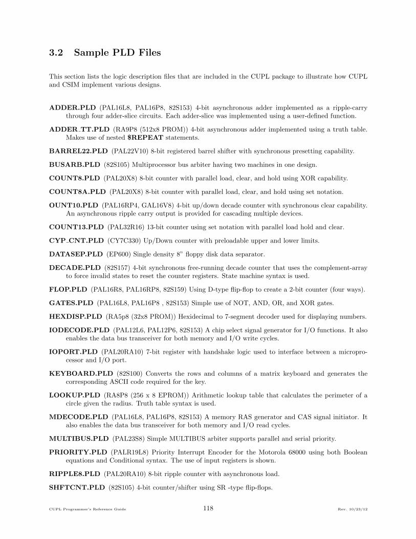
3.2 Sample PLD Files
This section lists the logic description files that are included in the CUPL package to illustrate how CUPLand CSIM implement various designs.
ADDER.PLD (PAL16L8, PAL16P8, 82S153) 4-bit asynchronous adder implemented as a ripple-carrythrough four adder-slice circuits. Each adder-slice was implemented using a user-defined function.
ADDER TT.PLD (RA9P8 (512x8 PROM)) 4-bit asynchronous adder implemented using a truth table.Makes use of nested $REPEAT statements.
BARREL22.PLD (PAL22V10) 8-bit registered barrel shifter with synchronous presetting capability.
BUSARB.PLD (82S105) Multiprocessor bus arbiter having two machines in one design.
COUNT8.PLD (PAL20X8) 8-bit counter with parallel load, clear, and hold using XOR capability.
COUNT8A.PLD (PAL20X8) 8-bit counter with parallel load, clear, and hold using set notation.
OUNT10.PLD (PAL16RP4, GAL16V8) 4-bit up/down decade counter with synchronous clear capability.An asynchronous ripple carry output is provided for cascading multiple devices.
COUNT13.PLD (PAL32R16) 13-bit counter using set notation with parallel load hold and clear.
CYP CNT.PLD (CY7C330) Up/Down counter with preloadable upper and lower limits.
DATASEP.PLD (EP600) Single density 8” floppy disk data separator.
DECADE.PLD (82S157) 4-bit synchronous free-running decade counter that uses the complement-arrayto force invalid states to reset the counter registers. State machine syntax is used.
FLOP.PLD (PAL16R8, PAL16RP8, 82S159) Using D-type flip-flop to create a 2-bit counter (four ways).
GATES.PLD (PAL16L8, PAL16P8 , 82S153) Simple use of NOT, AND, OR, and XOR gates.
HEXDISP.PLD (RA5p8 (32x8 PROM)) Hexidecimal to 7-segment decoder used for displaying numbers.
IODECODE.PLD (PAL12L6, PAL12P6, 82S153) A chip select signal generator for I/O functions. It alsoenables the data bus transceiver for both memory and I/O write cycles.
IOPORT.PLD (PAL20RA10) 7-bit register with handshake logic used to interface between a micropro-cessor and I/O port.
KEYBOARD.PLD (82S100) Converts the rows and columns of a matrix keyboard and generates thecorresponding ASCII code required for the key.
LOOKUP.PLD (RA8P8 (256 x 8 EPROM)) Arithmetic lookup table that calculates the perimeter of acircle given the radius. Truth table syntax is used.
MDECODE.PLD (PAL16L8, PAL16P8, 82S153) A memory RAS generator and CAS signal initiator. Italso enables the data bus transceiver for both memory and I/O read cycles.
MULTIBUS.PLD (PAL23S8) Simple MULTIBUS arbiter supports parallel and serial priority.
PRIORITY.PLD (PALR19L8) Priority Interrupt Encoder for the Motorola 68000 using both Booleanequations and Conditional syntax. The use of input registers is shown.
RIPPLE8.PLD (PAL20RA10) 8-bit ripple counter with asynchronous load.
SHFTCNT.PLD (82S105) 4-bit counter/shifter using SR -type flip-flops.
CUPL Programmer’s Reference Guide 118 Rev. 10/23/12

Figure Missing
Figure 3.10: Design with Simple Gates
SHFTCNT4.PLD (82S159) 4-bit counter/shifter using JK-type flip-flops.
SHFTCNT6.PLD (82S167) 4-bit counter/shifter using SR-type flip-flops.
STEPPER.PLD (PALT19R6) Memory mapped stepper motor controller interfaced to the 8048 single chipmicroprocessor.
TCOUNTER.PLD (EP600) 16-bit up/down counter with built-in shift register using toggle flip-flops.
TTL.PLD (PAL16L8) Multiple TTL chip representation using $Macros from the $Include file.
Any of these logic description files can be viewed or printed out, or they can be input to CUPL to generatedocumentation or download files. A corresponding test specification file (filename.SI) is also provided foreach logic description file, so that CSIM can be run to verify the designs.
The following examples describe key points of the following designs (the logic description file for each designis shown in parentheses):
• Simple gates (GATES.PLD)
• TTL conversion (WGTTL.PLD)
• Two-bit counter (FLOPS.PLD)
• Decade up/down counter using state-machine syntax (COUNT10.PLD)
• Seven-segment display decoder (HEXISP.PLD)
3.2.1 Example 1: Simple Gates
This example describes a design containing simple gates. Figure 3.10 shows the design.
The outputs are labeled to reflect the function of their gate; for example, the AND gate has an outputlabeled AND.
The following shows the CUPL source file (GATES.PLD provided in the CUPL package) that describes thedesign.
Name Gates;
Partno CA0001;
Date 07/16/87;
Designer G Woolheiser;
Company ATI;
Location San Jose , CA.;
Assembly Example;
CUPL Programmer’s Reference Guide 119 Rev. 10/23/12

/******************************************************/
/* */
/* This is an example to demonstrate how CUPL */
/* compiles simple gates . */
/* */
/******************************************************/
/* Target Devices: P16L8 , P16P8 , EP300 , and 82S153 */
/******************************************************/
/* Inputs: define inputs to build simple gates */
Pin 1 = a;
Pin 2 = b;
/* Outputs: define outputs as active HI levels
For PAL16L8 and PAL16LD8 , De Morgan ’s Theorem is
applied to invert all outputs due to fixed
inverting buffer in the device. */
Pin 12 = inva;
Pin 13 = invb;
Pin 14 = and;
Pin 15 = nand;
Pin 16 = or;
Pin 17 = nor;
Pin 18 = xor;
Pin 19 = xnor;
/* Logic: examples of simple gates expressed in CUPL */
inva = !a; /* inverters */
invb = !b;
and = a & b; /* and gate */
nand = !(a & b); /* nand gate */
or = a # b; /* or gate */
xor = a $ b; /* xor gate */
nor = !(a # b) /* nor gate */
xnor = !(a $ b); /* exclusive nor gate */
The first part of the file provides archival information and a description of the intended function of thedesign, including compatible PLDs.
Pin declarations are made corresponding to the inputs and outputs in the design diagram.
In the “Logic” section of the file, equations describe each of the gates in the design.
For the PAL16L8 and PAL16LD8 devices, which contain fixed inverting buffers, CUPL applies DeMorgan’sTheorem to invert all outputs because they were all declared active-HI in the pin list. For example, duringcompilation, CUPL converts the following equation for an OR gate, on an output pin that has been declaredas active high:
or = a # b ;
to the following single expanded product term (as shown in the documentation file):
or => !a & !b
CUPL Programmer’s Reference Guide 120 Rev. 10/23/12

Figure Missing
Figure 3.11: TTL Gate Representations and Boolean Equations
Figure Missing
Figure 3.12: TTL Schematic
3.2.2 Example 2: Converting a TTL Design to PLDs
This example shows how to use a PLD to replace existing TTL circuitry. The conversion requires translatingthe gates of a TTL logic design into equivalent Boolean logic equations, which can then be compiled byCUPL and assigned to a PLD.
Figure 3.11 shows the TTL gate representations used in designing logic systems and the correspondingBoolean equation for each gate.
The basic conversion rules shown in Figure 3.11 are sufficient to write equations for each gate within asystem of TTL gates when converting the logic to a PLD equivalent. CUPL uses an expression substitutionprocess to build larger equations from the smaller expressions representing each gate in the TTL schematic.Expression substitution permits approaching a schematic one gate at a time.
Figure 3.12 shows the schematic for the TTL logic that is converted in Example 1.
The TTL logic shown in Figure 3.12 performs the same address decoding and wait state generation as theWAITGEN.PLD file contained in the CUPL distribution package. The SAMPLE.PLD file created in the sampledesign session (see Part A of this chapter) is identical to WAITGEN.PLD.The PLD equivalent of this TTLcircuit replaces five to six packages with one device.The first step in the conversion process is to determinefrom the TTL schematic the logic that is to be placed in the PLD.
Figure 3.13 shows a PLD diagram equivalent to the TTL schematic with a box around the logic, and PLDpin number assignments.
Note that the outputs of the internal gates (those that do not connect to the PLD output pins) are arbitrarilylabeled with the variable names, A-H, to aid in entering equations in the logic description file. The logicdescription file used to convert this design is named WGTTL.PLD because it performs wait state generationand is based on a TTL design.
The following shows the contents of WGTTL.PLD.
Name Sample;
CUPL Programmer’s Reference Guide 121 Rev. 10/23/12

Figure Missing
Figure 3.13: PLD Equivalent Diagram
Partno P9000183;
Date 07/16/87;
Revision 02;
Designer Osann;
Company ATI;
Assembly PC Memory;
Location U106;
/********************************************************/
/* This device generates chip select signals for one */
/* 8Kx8 ROM and two 2Kx8 static RAMs. It also drives */
/* the system READY line to insert a wait -state of at */
/* least one cpu clock for ROM accesses */
/********************************************************/
/** Inputs **/
PIN 1 = cpu_clk ; /* CPU clock */
PIN [2..6] = [a15 ..11] ; /* CPU Address Bus */
PIN [7 8] = ![memw ,memr] ; /* Memory Data Strobes */
PIN 9 = reset ; /* System Reset */
PIN 11 = !oe ; /* Output enable */
/** Outputs **/
PIN 19 = !rom_cs ; /* ROM Chip Select */
PIN 18 = ready ; /* CPU ready signal */
PIN 15 = wait1 ; /* Start wait state */
PIN 14 = wait2 ; /* End wait state */
PIN [13 ,12] = ![ ram_cs1 ..0] ; /* RAM chip selects */
/** Declarations and Intermediate Variable Definitions **/
a = !(! memw) # !(! memr) ;
b = !a15 & !a14 ;
c = !a13 ;
d = !a12 & !a11 ;
e = !a11 ;
f = !a12 & !oe ;
g = !(! rom_cs # reset) ;
h = !(! memr) ;
/** Logic Equations **/
!rom_cs = !(h & b & c);
!ram_cs0 = !(a & b & a13 & d) ;
!ram_cs1 = !(a & b & a13 & f) ;
wait1.d = g ;
wait2.d = wait1 & g ;
ready.oe = !(!(h & b & c)) ;
ready = wait2 ;
The header information is identical to that in WAITGEN.PLD (and SAMPLE.PLD; see Part A), because the
CUPL Programmer’s Reference Guide 122 Rev. 10/23/12

functionality is the same.
The pin assignments match the schematic in Figure 3.13.
The logic equations for the internal gates are placed in the section of the file for “Declarations and Interme-diate Variable Definitions.” The equations in this section use the output variable names, A-H, assigned inthe schematic in Figure 3.13. For example, the AND gate LS02 is described by the following equation:
d = !a12 & !a11 ;
The equations in this section can be simplified. For example, the double negations can be eliminated in thefollowing equation:
a = !(! memw) # !(! memr) ;
by entering:
a = memw # memr ;
The section of the file “Logic Equations” contains equations that describe the output signals of the PLD.These equations are written in terms of the intermediate equations that describe the outputs of the internalgates. For example, the AND gate, LS10, has !ROM CS as its output signal, and the signals H, B and Cas inputs. Therefore, enter the following equation to describe LS10:
!rom_cs = !(h & b & c) ;
WGTTL.PLD to WAITGEN.PLD are not exactly alike, because the internal gates have been defined differently.When compiled, however, they perform the same function. This can be verified by simulating each logicdescription in turn with an identical simulation source file (WGTTL.SI and WAITGEN.SI provided in the CUPLpackage).
When converting a TTL design to a PLD, some slight changes in functionality are required. The asynchronousreset capability found on TTL flip-flops like the LS74 is not found in many of the commonly available PLDs.However, the same reset capability can be achieved by including a RESET variable in all product terms toensure a synchronous reset at the clock.
Therefore, WGTTL.PLD incorporates !RESET into the equation for G, which is used in the equations forboth WAIT1 (wait1.d = g;) and WAIT2 (wait2.d = wait1.d & g). Although the functional nature ofthe synchronous reset does differ in timing from that of the asynchronous reset, the synchronous reset issufficient for proper function of the device.
The simple methodology described in Example 2 allows the conversion of many TTL designs, especiallythose consisting of simple gates, to a PLD equivalent, regardless of the number of gate delays of TTL (logic)in the original design. In most cases, the only difference between the TTL design and the PLD is the totalpropagation delay through the circuit.
3.2.3 Example 3: Two-Bit Counter
This example demonstrates the implementation of a two-bit counter for a D-type flip-flop.
Figure 3.14 shows the timing diagram for the counter.
As indicated by the arrows, the registers are clocked on the rising edge of the clock signal.
CUPL Programmer’s Reference Guide 123 Rev. 10/23/12

Figure Missing
Figure 3.14: Two-Bit Counter Timing Diagram
The following shows the CUPL source file (FLOPS.PLD, provided in the CUPL package) to describe thetwo-bit counter design.
Name Flops;
Partno CA0002;
Revision 02;
Date 07/16/87;
Designer G. Woolheiser;
Company ATI;
Location None;
Assembly None;
/************************************************************/
/* */
/* This example demonstrates the use of D-type flip -flop */
/* to implement a two bit counter using the following */
/* timing diagram. */
/* ___ ___ ___ ___ ___ */
/* clock |___| |___| |___| |___| |___| */
/* _____ ________ ________ */
/* q0 /// |_______| |_______| |__ */
/* _____ ________________ */
/* q1 /// |_______________| |__ */
/* */
/* */
/* _________ */
/* reset |___________________________________ */
/* */
/************************************************************/
/* Target Devices: PAL16R8 , PAL16RP8 , GAL16V8 */
/************************************************************/
Pin 1 = clock;
Pin 2 = reset;
/* Outputs: define outputs and output active levels */
Pin 17 = q0;
Pin 16 = q1;
/* Logic: two bit counter using expanded exclusive
ors with d-type flip -flop */
qo.d = !reset & (!q0 & !q1
# !q0 & q1);
q1.d = !reset & (!q0 & q1
# q0 & !q1);
/* ANDed !reset defines a synchronous register reset */
The first part of the file provides archival information and a description of the intended function of thedesign, including compatible PLDs.
Pin declarations are made corresponding to the inputs and outputs in the design diagram.
CUPL Programmer’s Reference Guide 124 Rev. 10/23/12
Figure Missing
Figure 3.15: Up/Down Counter Diagram
In the “Logic” section of the file, equations are written to implement the counter. The equation for q0 iswritten to define when q0 asserts; that is, it defines the situation immediately before the rising clock edge.
The !reset term is used in the equations for both q0 and q1 to initialize the circuit, providing a synchronousreset. At power-on, the registers can be either high or low, as indicated by the DON’T CARE slashes in thetiming diagram (see Figure 3.14); the reset signal is initially asserted. By ANDing !reset into the equationfor each variable, the conditions are not met at power-on, so the registers do not set. Because the resetsignal returns LO (false) after the power-on process is complete, !reset is then true and does not affect thevalue of the registers at any other point in the circuit.
The .d extension in the equations specifies a D-type flip-flop. However, when an output is used as feedback,the .d extension is dropped. For example, if q0 is fed back to q1, an equation could be written as:
q1.d = q0 & !reset ;
not as:
q1.d = q0.d & !reset ;
or:
q1.d = q0.dq & !reset ;
3.2.4 Example 4: Decade Up/Down Counter
This example describes a four-bit up/down decade counter with a synchronous clear capacity. The counteralso provides an asynchronous ripple carry output for cascading multiple devices. The source file to implementthe counter uses CUPL state machine syntax.
Figure 3.15 shows the counter design and its state.
The input signal dir determines the direction of the count. When dir is high, the count goes down one oneach clock; when dir is low, the count goes up one on each clock. The clr signal performs a synchronousreset.
The following shows the CUPL source file (COUNT10.PLD, provided in the CUPL package) that implementsthe design.
Name Count10;
Partno CA0018;
Revision 02;
Date 07/16/87;
Designer Kahl;
CUPL Programmer’s Reference Guide 125 Rev. 10/23/12

Company ATI;
Location None;
Assembly None;
Device p16rp4;
/***********************************************************/
/* */
/* Decade Counter */
/* This is a 4-bit up/down decade counter with */
/* synchronous clear capability. An asynchronous */
/* ripple carry output is provided for cascading */
/* multiple devices. CUPL state machine syntax */
/* is used */
/***********************************************************/
/* Allowable Target Device Types: PAL16RP4 , GAL16V8 , EP300 */
/************************************************************/
/** Inputs **/
Pin 1 = clk; /* counter clock */
Pin 2 = clr; /* counter clear input */
Pin 3 = dir; /* counter direction input */
Pin 11 = !oe; /* Register output enable */
/* Outputs */
Pin [14..17] = [Q3 ..0]; /* counter outputs */
Pin 18 = carry; /* ripple carry out */
/* Declarations and Intermediate Variable Definitions */
field count = [Q3 ..0]; /* declare counter bit field */
$define S0 ’b’0000
$define S1 ’b’0001
$define S2 ’b’0010
$define S3 ’b’0011
$define S4 ’b’0100
$define S5 ’b’0101
$define S6 ’b’0110
$define S7 ’b’0111
$define S8 ’b’1000
$define S9 ’b’1001
field node = [clr ,dir]; /* declare filed node control */
up = mode :0; /* define count up mode */
down = mode :1; /* define count down mode */
clear = mode :2..3]; /* define count clear mode */
/* Logic Equations */
sequence count { /* free running counter */
present S0 if up next S1;
if down next S9;
if clear next S0;
present S1 if up next S2;
if down next S0;
if clear next S0;
present S2 if up next S3;
if down next S1;
if clear next S0;
present S3 if up next S4;
if down next S2;
if clear next S0;
present S4 if up next S5;
if down next S3;
if clear next S0;
present S5 if up next S6;
if down next S4;
if clear next S0;
present S6 if up next S7;
if down next S5;
if clear next S0;
CUPL Programmer’s Reference Guide 126 Rev. 10/23/12
present S7 if up next S8;
if down next S6;
if clear next S0;
present S8 if up next S9;
if down next S7;
if clear next S0;
present S9 if up next S0;
if down next S8;
if clear next S0;
out carry; /* assert carry output */
The first part of the file provides archival information and a description of the intended function of thedesign, including compatible PLDs.
Pin declarations are made corresponding to the inputs and outputs in the design diagram.
The “Declarations and Intermediate Variable Definitions” section contains declarations that simplifythe notation.
The name “count” is assigned to the output variables Q3, Q2, Q1, and Q0.
The $DEFINE command is used to assign names to ten binary states representing the state machine output.The state name can then be used in the logic equations to represent the corresponding binary number.
The FIELD keyword is used to combine the clr and dir inputs into a set called mode. Mode is definedby the following equations:
up = mode :0;
down = mode :1;
clear = mode [2..3];
Mode represents the inputs clr and dir, so the three equations above are equivalent to the followingequations:
up = !clr & !dir ;
down = !clr & dir ;
clear = (clr & !dir) # (clr & dir) ;
The three modes are defined as follows:
up - Both the dir and clr inputs are not asserted.
down - The dir input is asserted and clr is not asserted.
clear - The clr input is asserted and dir is either asserted or not asserted.
The “Logic Equations” section contains the state machine syntax that specifies the states in the counter.In the first line, the SEQUENCE keyword identifies count (that is, Q3, Q2, Q1, and Q0) as the outputsto which the state values apply.
Conditional statements have been written to specify the transition from each possible present state to a nextstate, for each of the three modes. For example, when the present state is S4, if the mode is up, the countergoes to S5; if the mode is down the counter goes to S3; or if the mode is clear, the counter goes to S0. Asexample 4 shows, one advantage of the state machine syntax is that it clearly documents the operation ofthe design.
In Example 4, state 0 (binary value 0000) is defined, because it is the result of the clr signal. It is rec-ommended that all designs have a valid 0000 defined to avoid being stuck at state 0. For example, in this
CUPL Programmer’s Reference Guide 127 Rev. 10/23/12

design, if a state that hasn’t been defined occurs at power-on, such as hexadecimal A-F, none of the condi-tions described in the equations is met, so the state goes to state 0 (hex value 0000). If 0000 has not beendefined as a valid state, the counter stays at state 0.
The following shows how this example could have been written as a virtual design. It is the same file, butit has been modified where necessary to show the difference between a virtual design and a device specificdesign.
Name Count10;
Partno CA0018;
Revision 02;
Date 07/16/87;
Designer Kahl;
Company ATI;
Location None;
Assembly None;
Device VIRTUAL;
/***********************************************************/
/* */
/* Decade Counter */
/* This is a 4-bit up/down decade counter with */
/* synchronous clear capability. An asynchronous */
/* ripple carry output is provided for cascading */
/* multiple devices. CUPL state machine syntax */
/* is used */
/***********************************************************/
/* Allowable Target Device Types: PAL16RP4 , GAL16V8 , EP300 */
/************************************************************/
/** Inputs **/
Pin = clk; /* counter clock */
Pin = clr; /* counter clear input */
Pin = dir; /* counter direction input */
Pin = !oe; /* Register output enable */
/* Outputs */
Pin = [Q3..0]; /* counter outputs */
Pin = carry; /* ripple carry out */
/* Declarations and Intermediate Variable Definitions */
field count = [Q3 ..0]; /* declare counter bit field */
$define S0 ’b’0000
$define S1 ’b’0001
$define S2 ’b’0010
$define S3 ’b’0011
$define S4 ’b’0100
$define S5 ’b’0101
$define S6 ’b’0110
$define S7 ’b’0111
$define S8 ’b’1000
$define S9 ’b’1001
field node = [clr ,dir]; /* declare filed node control */
up = mode :0; /* define count up mode */
down = mode :1; /* define count down mode */
clear = mode :2..3]; /* define count clear mode */
/* Logic Equations */
sequence count { /* free running counter */
present S0 if up next S1;
if down next S9;
if clear next S0;
present S1 if up next S2;
if down next S0;
if clear next S0;
CUPL Programmer’s Reference Guide 128 Rev. 10/23/12

present S2 if up next S3;
if down next S1;
if clear next S0;
present S3 if up next S4;
if down next S2;
if clear next S0;
present S4 if up next S5;
if down next S3;
if clear next S0;
present S5 if up next S6;
if down next S4;
if clear next S0;
present S6 if up next S7;
if down next S5;
if clear next S0;
present S7 if up next S8;
if down next S6;
if clear next S0;
present S8 if up next S9;
if down next S7;
if clear next S0;
present S9 if up next S0;
if down next S8;
if clear next S0;
out carry; /* assert carry output */
It is possible to use some of the features of the CUPL preprocessor to considerably shorten this PLD file.The following will show how this same file could be written with a $REPEAT structure which reduces thefile size considerably.
Name Count10;
Partno CA0018;
Revision 02;
Date 07/16/87;
Designer Kahl;
Company ATI;
Location None;
Assembly None;
Device VIRTUAL;
/***********************************************************/
/* */
/* Decade Counter */
/* This is a 4-bit up/down decade counter with */
/* synchronous clear capability. An asynchronous */
/* ripple carry output is provided for cascading */
/* multiple devices. CUPL state machine syntax */
/* is used */
/***********************************************************/
/* Allowable Target Device Types: PAL16RP4 , GAL16V8 , EP300 */
/***********************************************************/
/** Inputs **/
Pin = clk; /* counter clock */
Pin = clr; /* counter clear input */
Pin = dir; /* counter direction input */
Pin = !oe; /* Register output enable */
/* Outputs */
Pin = [Q3..0]; /* counter outputs */
Pin = carry; /* ripple carry out */
/* Declarations and Intermediate Variable Definitions */
field count = [Q3 ..0]; /* declare counter bit field */
CUPL Programmer’s Reference Guide 129 Rev. 10/23/12
Figure Missing
Figure 3.16: Seven-Segment Display Decoder
field node = [clr ,dir]; /* declare filed node control */
up = mode :0; /* define count up mode */
down = mode :1; /* define count down mode */
clear = mode :2..3]; /* define count clear mode */
/* state machine description */
sequence count {
present 0
if up & !clear next 1;
if down & !clear next 9;
if clear next 0;
$REPEAT i=[1..9]
present i
if up & !clear next {(i+1)%10};
if down & !clear next {(i -1)%10}
if clear next 0;
$REPEND
In this variation, we removed the $DEFINE statements because we use the raw numbers instead. Themost significant change is that we used a $REPEAT loop to define most of the states instead of definingeach state individually. It is possible to do this because all the states are identical except for the next statethat each goes to. Notice that we define state 0 by itself and then all the other states are defined in one$REPEAT loop.The $REPEAT loop expands upon compilation to give a definition for each state. Noticethat the statement indicating the next state is given as a calculation from the repeat variable ’i’. In theloop, ’i’ represents the number of the current state. The next state is therefore ’i+1’. This will work for allstates except the last state. In the last state, the state machine must go back to state 0. To accomplish this,the formula to calculate the next state is given as ‘(i+1)%10’. This means ’i+1’ ‘modulo 10. The number10 represents the number of states. Therefore, when in state 9 the next state is calculated as 9+1 = 10 thenmodulo 10 which gives 0. A similar condition occurs in calculating the previous state except that we subtract1 instead of adding it. You might have noticed that we defined state 0 separately. This was done becausethe $REPEAT variables can only handle positive numbers. If we had defined state 0 in the $REPEATloop this would result in evaluating to next state -1 and the compiler would produce an unexpected result.
3.2.5 Example 5: Seven-Segment Display Decoder
This example shows a hexadecimal-to-seven-segment decoder for driving common-anode LEDs. The designincorporates both a ripple-blanking input to inhibit the display of leading zeroes, and a ripple-blankingoutput for easy cascading of digits.
Figure 3.16 shows the segment display decoder.
The segments in the display, labeled a-g, correspond to the outputs in the diagram.
CUPL Programmer’s Reference Guide 130 Rev. 10/23/12

The following shows the source file (HEXDISP.PLD, provided with the CUPL package).
Name Hexdisp;
Partno CA0007;
Revision 02;
Date 07/16/87;
Designer T. Kahl;
Company ATI;
Location None;
Assembly None;
/**************************************************************/
/* */
/* a */
/* This is a hexadecimal -to-seven -segment ----- */
/* decoder capable of driving common -anode | | */
/* LEDs. It incorporates both a ripple - f| |b */
/* blanking input (to inhibit displaying | g | */
/* leading zeroes) and a ripple blanking output ----- */
/* to allow for easy cascading of digits | | */
/* e| |c */
/* | | */
/* ----- */
/* d */
/* */
/**************************************************************/
/* Allowable Target Device Types: 32 x 8 PROM (82 S123 or */
/* equivalent */
/**************************************************************/
/** Input group (Note this is only a comment) **/
pin [10..13] = [D0 ..3]; /* data input lines to display */
pin 14 = !rbi; /* ripple blanking input */
/** Output Group ( Note this is only a comment ) **/
pin [7..1] = ![a,b,c,d,e,f,g]; /* Segment output lines */
pin 9 = !rbo; /* Ripple Blanking output */
/** Declarations and Intermediate Variable Definitions */
field data = [D3..0]; /* hexadecimal input field */
field segment =[a,b,c,d,e,f,g]; /* Display segment field */
$define ON ’b’1 /* segment lit when logically"ON" */
$define OFF ’b’0 /* segment dark when logically "OFF" */
The first part of the file provides archival information and a description of the intended function of thedesign, including compatible PLDs.
Pin declarations are made corresponding to the inputs and outputs in the design diagram.
In the “Declarations and Intermediate Variables” section, field assignments are made to group the input pinsinto a set named data and the output pins into a set named segment. ON and OFF are defined respectivelyas binary 1 and binary 0.
/** Logic Equations **/
/* a b c d e f g */
segment =
/* 0 */ [ ON, ON, ON, ON , ON, ON, OFF] & data:0 & !rbi
/* 1 */ # [OFF , ON , ON, OFF , OFF , OFF , OFF] & data:1
/* 2 */ # [ ON , ON, OFF , ON, ON, OFF , ON] & data:2
/* 3 */ # [ ON , ON, ON, ON, OFF , OFF , ON] & data:3
/* 4 */ # [OFF , ON , ON, OFF , OFF , ON , ON] & data:4
/* 5 */ # [ ON , OFF , ON, ON, OFF , ON, ON] & data:5
/* 6 */ # [ ON , OFF , ON, ON, ON, ON, ON] & data:6
/* 7 */ # [ ON , ON, ON, OFF , OFF , OFF , ON] & data:7
/* 8 */ # [ ON , ON, ON, ON, ON , ON , OFF] & data:8
CUPL Programmer’s Reference Guide 131 Rev. 10/23/12

/* 9 */ # [ ON , ON, ON, ON, OFF , ON, ON] & data:9
/* A */ # [ ON , ON, ON, OFF , ON, ON, ON] & data:A
/* B */ # [OFF , OFF , ON , ON , ON, ON, ON] & data:B
/* C */ # [ ON , OFF , OFF , ON , ON, ON, OFF] & data:C
/* D */ # [OFF , ON , ON, ON, ON, OFF , ON] & data:D
/* E */ # [ ON , OFF , OFF , ON , ON, ON, ON] & data:E
/* F */ # [ ON , OFF , OFF , OFF , ON , ON , ON] & data:F;
rbo = rbi & data :0;
The logic equations are set up as a function table to describe the segments that are lit up by each inputpattern. Comments create a header for the function table, listing the output segments across the top andthe input numbers vertically down the side.
Each line of the table describes a decoded hex value and the segments of the display that the hex value turnson or off. For example, the line for an input value of 4 is written as follows:
[OFF , ON, ON, OFF , OFF , ON, ON] & data:4
The function table format expresses the intent of the design more clearly than equations; that is, the exampleabove shows that an input value of 4 turns segment a off, segment b on, segment c on, and so on.
3.2.6 Example 6: 4-Bit Counter With Load and Reset
This example will present a counter that can be loaded and reset. The design is done using the VIRTUALdevice but it could easily be implemented in almost any PLD that has four or more registers.
Name Counter;
Partno FL1201;
Revision 01;
Date 08/26/91;
Designer RGT;
Company LDI;
Location None;
Assembly None;
Device VIRTUAL;
/*******************************************/
/* 4-bit counter */
/*******************************************/
/** inputs **/
PIN = clk; /* clock signal for registers */
PIN = load ;/* load signal */
PIN = !ClrFlag;
PIN = [LoadPin0 ..3]; /* pins from which to load data */
/** outputs **/
PIN = [CountPin0 ..3];
/* intermediate variables and fields */
field STATE_BITS = [Count0 ..3];
field LOAD_BUS = [LoadPin0 ..3];
/** state machine definition **/
SequenceD STATE_BITS {
/* build a repeated loop for the states */
$REPEAT i = [0..15]
Present ’h’{i}
/* go to state 0 if clear signal is true */
/* if the load signal is false go to the *
* next state. Note that the next state *
CUPL Programmer’s Reference Guide 132 Rev. 10/23/12

* is (current state + 1) modulo 16. *
* This causes the counter to wrap back *
* to 0 when in the last state */
If !load Next ’h’{(i+1)%16};
If !load & ClrFlag Next ’b’0;
$REPEND
/* Add the load capability by using the *
* APPEND statement. This has the effect of *
* adding more inputs to the OR gate for *
* this output. This equation states that if *
* the load signal is true then the counter *
* registers are loaded with data from the *
* load pins. This is why ’load ’ was used in *
* the equations for the ’IF’ statements in *
* the state definitions. */
APPEND STATE_BITS.d = load & LOAD_BUS;
Since this is a virtual design, pin numbering can be ignored. The signals to be used are declared withoutany pin numbers.
When the load signal is asserted, the values at the load pins are fed into the state bit registers. When the‘Clear’ signal is asserted, the state machine is forced to state 0.
The $REPEAT loop is defined as [0 ..15]. Inside the loop, the present state is defined as ’h’{i}. Thiscauses the numbers to be evaluated as hex numbers. The expansion that results from this is a state machinewith 16 states ranging from 0 to F in hexadecimal. If the ’h’ was left off, the states would have beenexpanded as 0 to 15 in decimal. The compiler would have interpreted these as hex anyway and states A-Fwould not have been defined. Additionally, State 10 in hex cannot exist with this number of statebits sincethat would require 5 statebits but all that we have is 4.
Notice that all the IF statements are anded with “!load”. This was done because we want to give loadingthe highest possible priority. Also this removes any possible conflict that could occur if load and some othersignal were asserted at the same time.
The next state is calculated as (present state + 1) modulo 16. This causes the counter to wrap back to thezero state when it is in the last state. We use modulo 16 because this is the number of states in the statemachine.
The last part of this design involves adding the load capability to our design. For this we use the APPENDstatement. The append statement causes the expression given to be ORed to the variable specified. Thisentire state machine eventually becomes a set of equations for each of the state bits. Our intent is to addanother condition where the registers are loaded with the value from a set of input pins. Remember thatwe used ‘!load’ in all the IF statements. That was to make sure that the equations generated by those IFstatements, would not conflict with the APPEND statement.
Equations Before APPEND
CountPin0.d = !load & ???.....
# !load & ???.....;
Equations After APPEND
CountPin0.d = !load & ???.....
# !load & ???.....
# load & LoadPin0;
CUPL Programmer’s Reference Guide 133 Rev. 10/23/12

As an exercise, try to add up/down capability to this example. Also, try implementing it into an actualdevice.
CUPL Programmer’s Reference Guide 134 Rev. 10/23/12