cu wire bonding bruker nano surfaces contourgt 3d · pdf fileassisting the transition to cu...
TRANSCRIPT
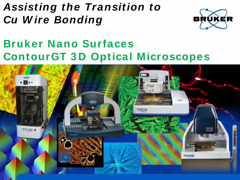
Assisting the Transition to Cu Wire Bonding Bruker Nano Surfaces ContourGT 3D Optical Microscopes
Outline Transition to Cu Wire Bonding
• Drivers to Cu Wirebonding Adoption
– Overview – Cost driver – Improved reliability
/mechanical stability – Electrical and thermal
properties
• Cu Wirebonding Challenges
– Material challenges – Precise control for force and
ultrasonic nergy – Current monitoring methods
• Bruker ContourGT 3D Microscope Solution
– Fastest time to 3D data – Automated/streamlined
computations – Benefits to Cu wire bonder
setup (force/current/flow, etc.) – Benefits as process monitoring
tool
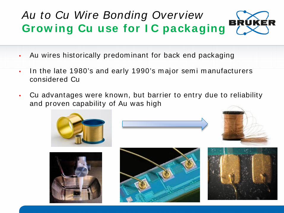
Au to Cu Wire Bonding Overview Growing Cu use for IC packaging
• Au wires historically predominant for back end packaging
• In the late 1980’s and early 1990’s major semi manufacturers considered Cu
• Cu advantages were known, but barrier to entry due to reliability and proven capability of Au was high
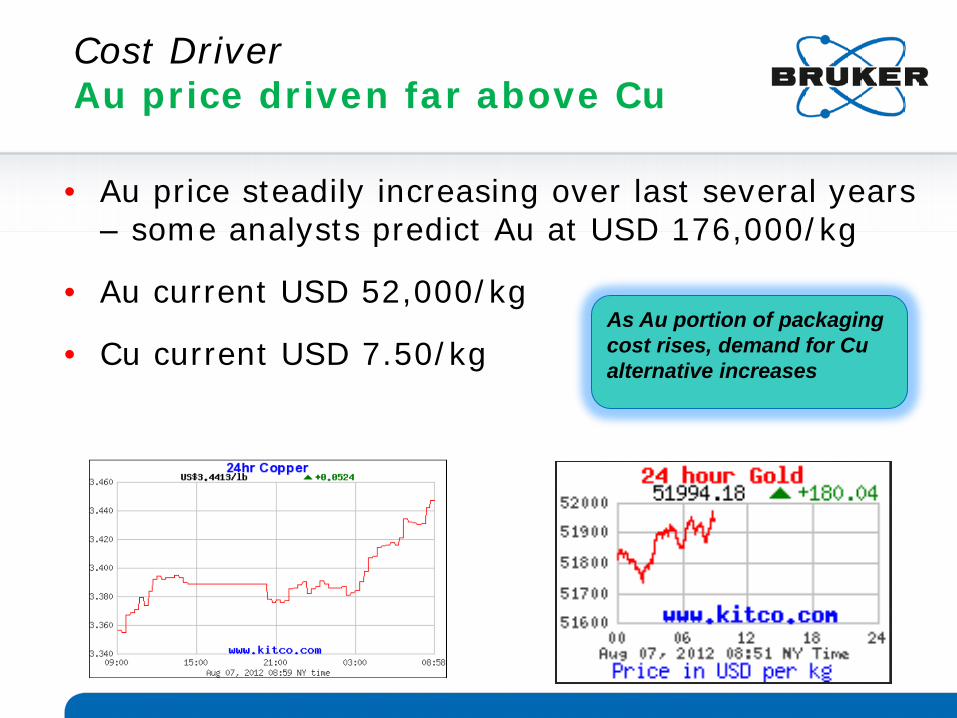
Cost Driver Au price driven far above Cu
• Au price steadily increasing over last several years – some analysts predict Au at USD 176,000/kg
• Au current USD 52,000/kg
• Cu current USD 7.50/kg As Au portion of packaging cost rises, demand for Cu alternative increases
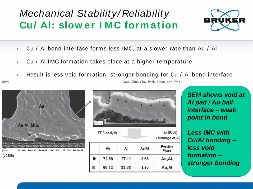
Mechanical Stability/Reliability Cu/Al: slower IMC formation
• Cu / Al bond interface forms less IMC, at a slower rate than Au / Al
• Cu / Al IMC formation takes place at a higher temperature
• Result is less void formation, stronger bonding for Cu / Al bond interface
SEM shows void at Al pad / Au ball interface – weak point in bond Less IMC with Cu/Al bonding – less void formation – stronger bonding
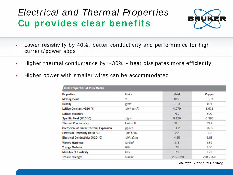
Electrical and Thermal Properties Cu provides clear benefits
• Lower resistivity by 40%, better conductivity and performance for high current/power apps
• Higher thermal conductance by ~30% - heat dissipates more efficiently
• Higher power with smaller wires can be accommodated
Source: Heraeus Catalog
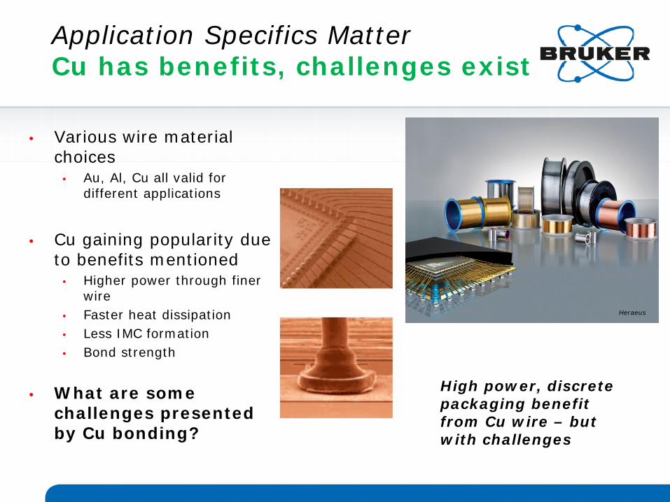
Application Specifics Matter Cu has benefits, challenges exist
• Various wire material choices
• Au, Al, Cu all valid for different applications
• Cu gaining popularity due
to benefits mentioned • Higher power through finer
wire • Faster heat dissipation • Less IMC formation • Bond strength
• What are some challenges presented by Cu bonding?
Heraeus
High power, discrete packaging benefit from Cu wire – but with challenges
Challenges to Cu Wire Bonding Hardness of FAB
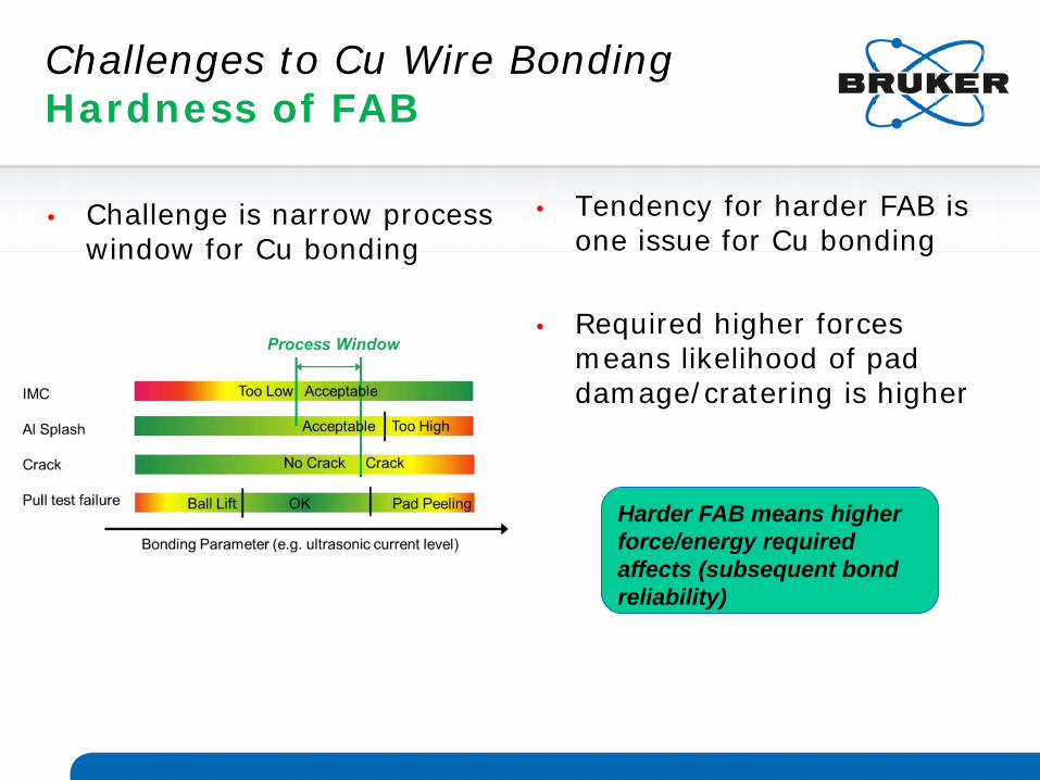
• Challenge is narrow process window for Cu bonding
• Tendency for harder FAB is one issue for Cu bonding
• Required higher forces means likelihood of pad damage/cratering is higher
Harder FAB means higher force/energy required affects (subsequent bond reliability)
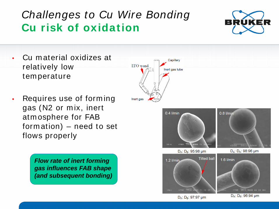
• Cu material oxidizes at relatively low temperature
• Requires use of forming gas (N2 or mix, inert atmosphere for FAB formation) – need to set flows properly
Challenges to Cu Wire Bonding Cu risk of oxidation
Flow rate of inert forming gas influences FAB shape (and subsequent bonding)
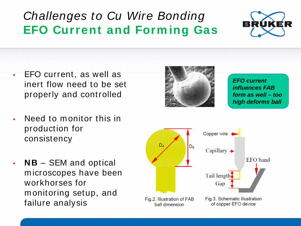
• EFO current, as well as
inert flow need to be set properly and controlled
• Need to monitor this in production for consistency
• NB – SEM and optical microscopes have been workhorses for monitoring setup, and failure analysis
Challenges to Cu Wire Bonding EFO Current and Forming Gas
EFO current influences FAB form as well – too high deforms ball
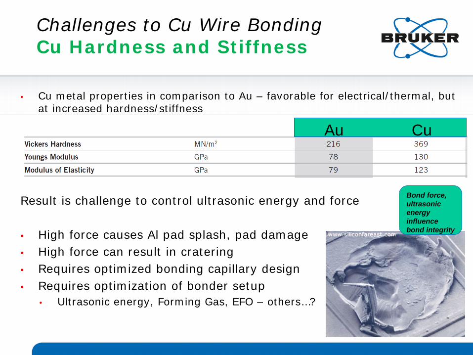
• Cu metal properties in comparison to Au – favorable for electrical/thermal, but at increased hardness/stiffness
Result is challenge to control ultrasonic energy and force
• High force causes Al pad splash, pad damage • High force can result in cratering • Requires optimized bonding capillary design • Requires optimization of bonder setup
• Ultrasonic energy, Forming Gas, EFO – others…?
Challenges to Cu Wire Bonding Cu Hardness and Stiffness
Au Cu
Bond force, ultrasonic energy influence bond integrity
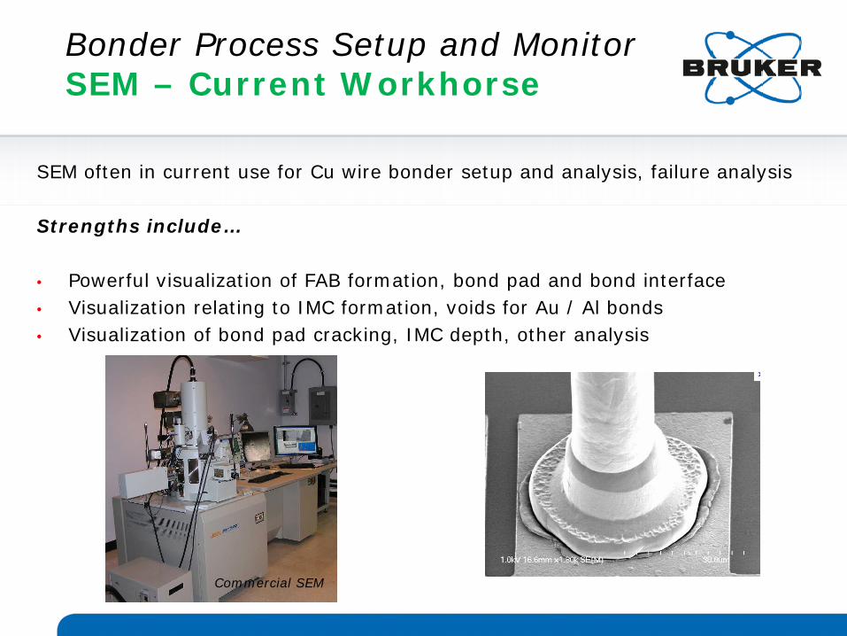
SEM often in current use for Cu wire bonder setup and analysis, failure analysis Strengths include… • Powerful visualization of FAB formation, bond pad and bond interface • Visualization relating to IMC formation, voids for Au / Al bonds • Visualization of bond pad cracking, IMC depth, other analysis
Commercial SEM
Bonder Process Setup and Monitor SEM – Current Workhorse
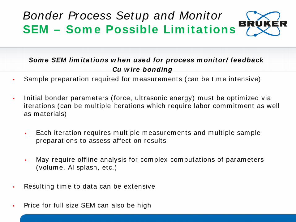
Some SEM limitations when used for process monitor/feedback Cu wire bonding • Sample preparation required for measurements (can be time intensive)
• Initial bonder parameters (force, ultrasonic energy) must be optimized via
iterations (can be multiple iterations which require labor commitment as well as materials) • Each iteration requires multiple measurements and multiple sample
preparations to assess affect on results • May require offline analysis for complex computations of parameters
(volume, Al splash, etc.)
• Resulting time to data can be extensive
• Price for full size SEM can also be high
Bonder Process Setup and Monitor SEM – Some Possible Limitations
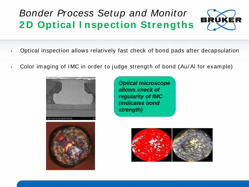
• Optical inspection allows relatively fast check of bond pads after decapsulation
• Color imaging of IMC in order to judge strength of bond (Au/Al for example)
Bonder Process Setup and Monitor 2D Optical Inspection Strengths
Optical microscope allows check of regularity of IMC (indicates bond strength)
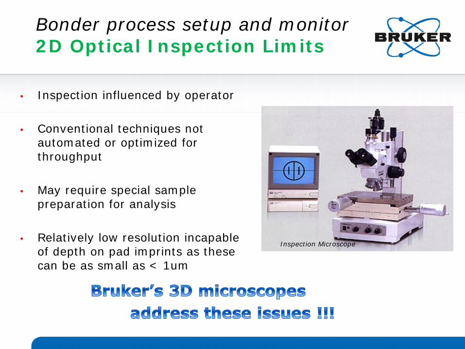
• Inspection influenced by operator
• Conventional techniques not automated or optimized for throughput
• May require special sample preparation for analysis
• Relatively low resolution incapable of depth on pad imprints as these can be as small as < 1um
Bonder process setup and monitor 2D Optical Inspection Limits
Inspection Microscope
Bruker 3D Optical Microscope Checklist of Advantages
• Fast
• Excellent vertical resolution
• Minimized sample prep for imprint/cavity depth study
• Accurate and gage capable metrology instrument lends to process monitoring
• Operator Interface For Streamlined, Simplified Use
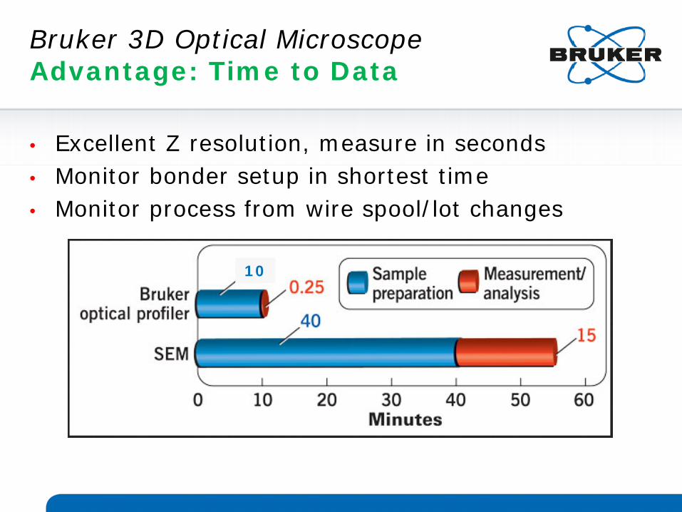
Bruker 3D Optical Microscope Advantage: Time to Data
• Excellent Z resolution, measure in seconds • Monitor bonder setup in shortest time • Monitor process from wire spool/lot changes
10
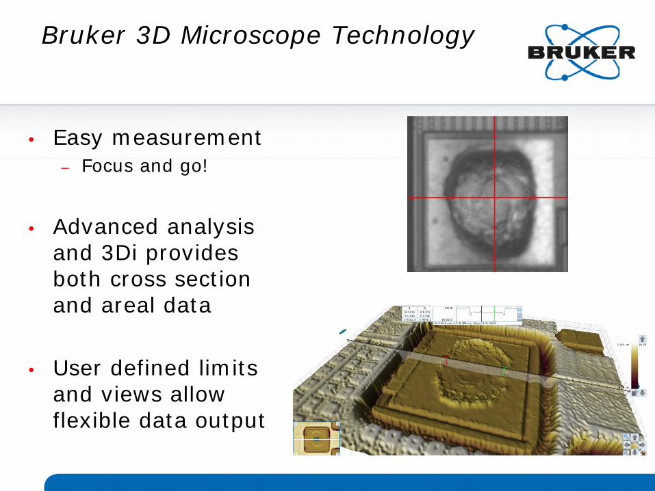
Bruker 3D Microscope Technology
• Easy measurement – Focus and go!
• Advanced analysis
and 3Di provides both cross section and areal data
• User defined limits and views allow flexible data output
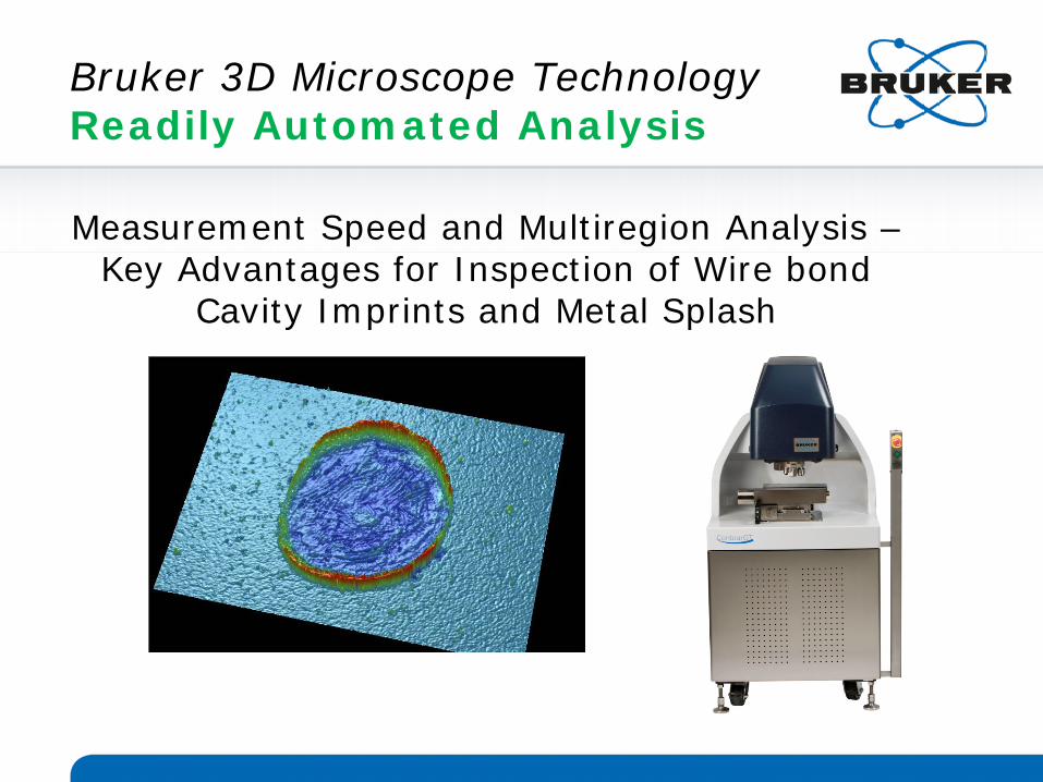
Measurement Speed and Multiregion Analysis – Key Advantages for Inspection of Wire bond
Cavity Imprints and Metal Splash
Bruker 3D Microscope Technology Readily Automated Analysis
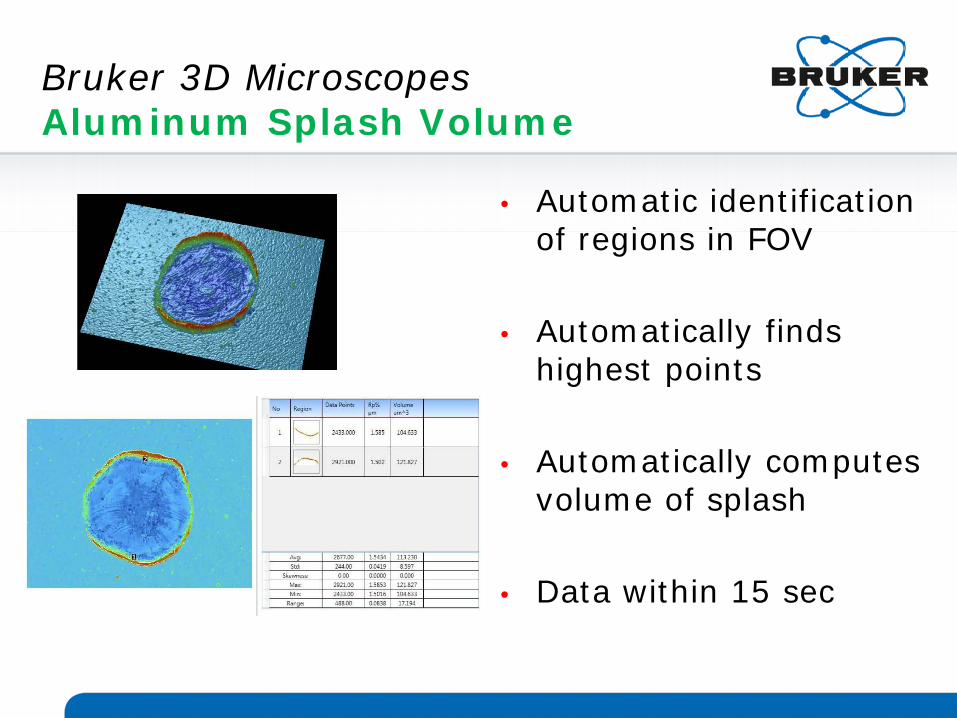
Bruker 3D Microscopes Aluminum Splash Volume
• Automatic identification of regions in FOV
• Automatically finds highest points
• Automatically computes volume of splash
• Data within 15 sec
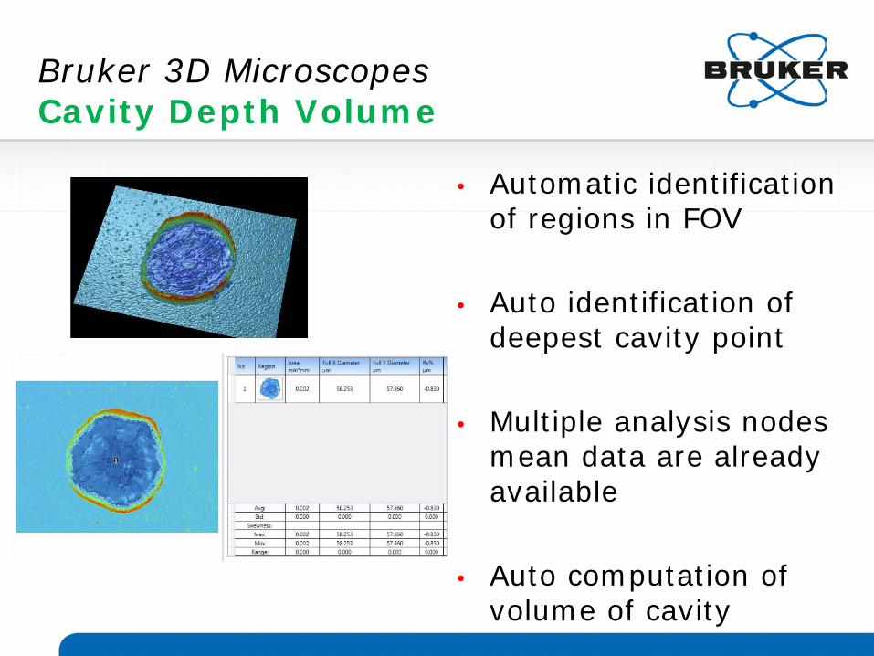
Bruker 3D Microscopes Cavity Depth Volume
• Automatic identification of regions in FOV
• Auto identification of deepest cavity point
• Multiple analysis nodes mean data are already available
• Auto computation of volume of cavity
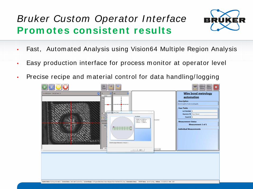
Bruker Custom Operator Interface Promotes consistent results
• Fast, Automated Analysis using Vision64 Multiple Region Analysis
• Easy production interface for process monitor at operator level
• Precise recipe and material control for data handling/logging
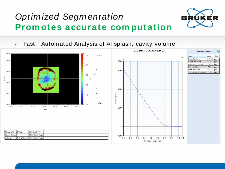
Optimized Segmentation Promotes accurate computation
• Fast, Automated Analysis of Al splash, cavity volume
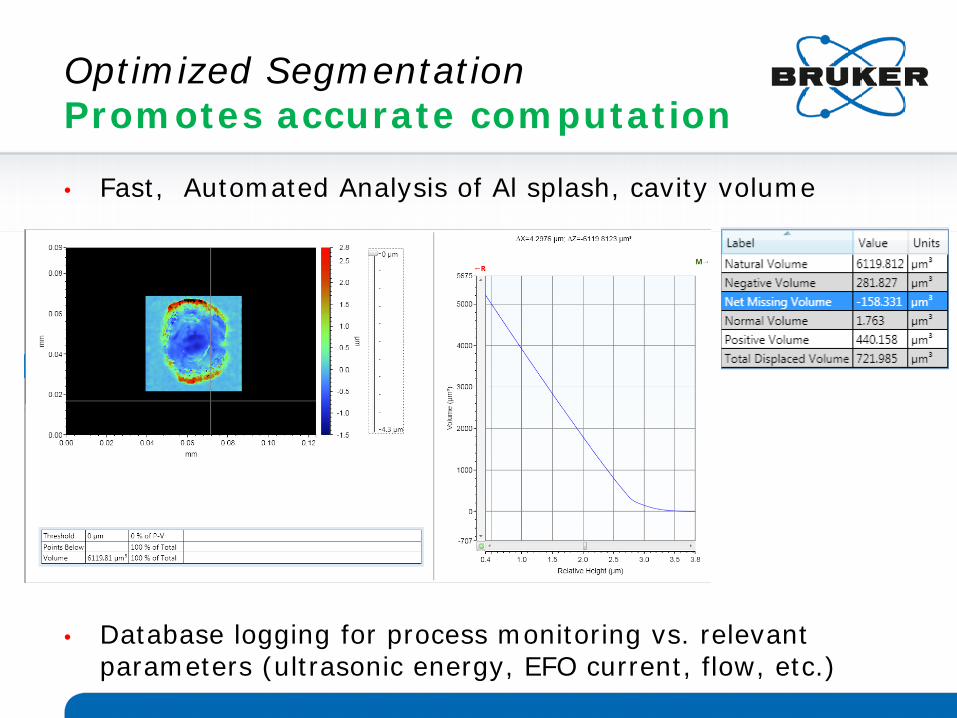
Optimized Segmentation Promotes accurate computation
• Fast, Automated Analysis of Al splash, cavity volume
• Database logging for process monitoring vs. relevant parameters (ultrasonic energy, EFO current, flow, etc.)
Summary of Benefits Fast, Accurate Metrology
• Bruker 3D Microscopes offer fastest time to data for monitoring of imprints/bond depth/Al splash
• Close to line, accurate data readily available vs. other inspection and monitor methods
• Automation for multiple point inspections with Bruker tools is simple and easy to define
• Gage-capable tool means minimum iterations for setup and also reliable monitoring of bonding platforms

Summary of Benefits Versatile Metrology for Customer Solutions
THANK YOU!!!
Questions??
THANK YOU!!!
[email protected] +1 520 741 1044 x 1061 [email protected] Matt Novak, Ph.D. Market Applications Development Manager Bruker NSD, SOM www.bruker-axs.com