coreaxi v3.2 handbook - actel.com slave 0 if axi slave 15 if axi master0 if axi master1 if ... the...
TRANSCRIPT

CoreAXI v3.2 Handbook
CoreAXI v3.2 Handbook 1
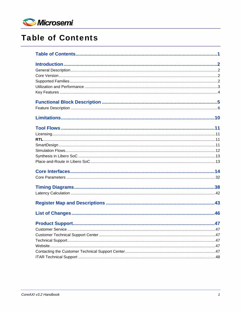
Table of Contents
Table of Contents ........................................................................................................... 1
Introduction .................................................................................................................... 2 General Description ....................................................................................................................................... 2 Core Version .................................................................................................................................................. 2 Supported Families ........................................................................................................................................ 2 Utilization and Performance .......................................................................................................................... 3 Key Features ................................................................................................................................................. 4
Functional Block Description ....................................................................................... 5 Feature Description ....................................................................................................................................... 6
Limitations .................................................................................................................... 10
Tool Flows .................................................................................................................... 11 Licensing ...................................................................................................................................................... 11 RTL .............................................................................................................................................................. 11 SmartDesign ................................................................................................................................................ 11 Simulation Flows.......................................................................................................................................... 12 Synthesis in Libero SoC .............................................................................................................................. 13 Place-and-Route in Libero SoC ................................................................................................................... 13
Core Interfaces ............................................................................................................. 14 Core Parameters ......................................................................................................................................... 32
Timing Diagrams .......................................................................................................... 38 Latency Calculation ..................................................................................................................................... 42
Register Map and Descriptions .................................................................................. 43
List of Changes ............................................................................................................ 46
Product Support ........................................................................................................... 47 Customer Service ........................................................................................................................................ 47 Customer Technical Support Center ........................................................................................................... 47 Technical Support ........................................................................................................................................ 47 Website ........................................................................................................................................................ 47 Contacting the Customer Technical Support Center ................................................................................... 47 ITAR Technical Support .............................................................................................................................. 48

CoreAXI v3.2 Handbook 2
Introduction
General Description The CoreAXI v3.2 is a multi-master multiple-slave AXI3 bus interconnect.
CoreAXI
AXI Slave 0 IF
AXI Slave 15 IF
AXI Master0 IF
AXI Master1 IF
AXI Master2 IF
AXI Master3 IF
AXI Slave 16 IF
:
:
Figure 1 CoreAXI Block Diagram
The CoreAXI supports up to four AXI master interfaces and 16 AXI slave interfaces. The number of AXI master and slaves to be connected is programmable through parameter configuration. Each slave gets a maximum of 256 MB of address space. Alternatively, a huge slave of 2 GB can also be configured if larger slave region is required. Also, the slaves can be combined to form much bigger slave region. The AXI protocol defines five independent channels: Write address channel, Read address channel, Write data channel, Write response channel, and Read data channel. Refer to the AMBA3 AXI specification document for more details.
Core Version This Handbook applies to CoreAXI version 3.2.
Supported Families • RTG4™ • SmartFusion®2 • IGLOO®2
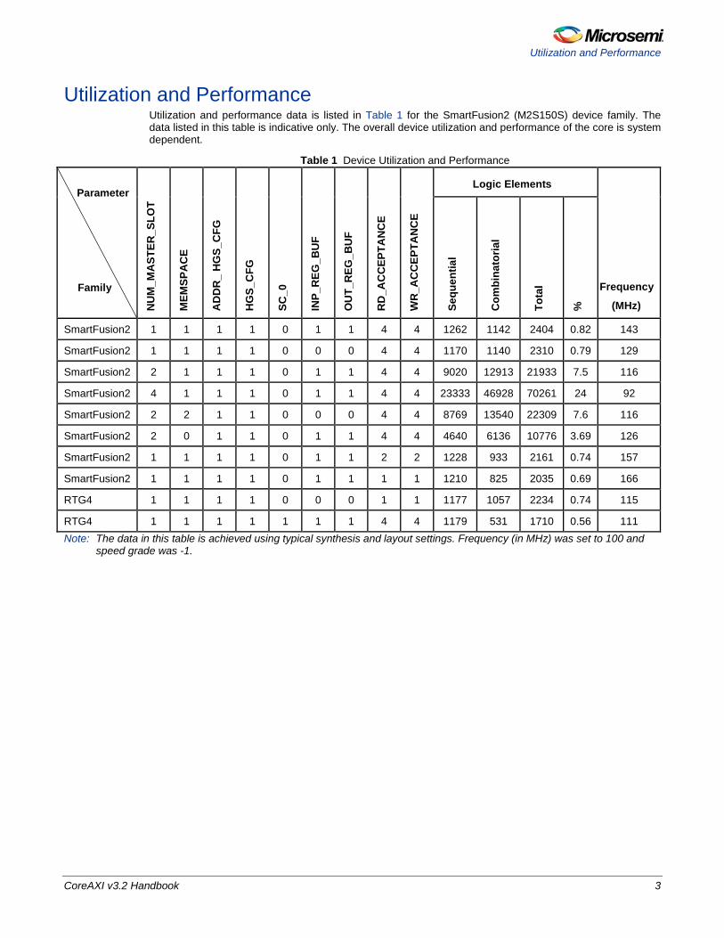
Utilization and Performance
CoreAXI v3.2 Handbook 3
Utilization and Performance Utilization and performance data is listed in Table 1 for the SmartFusion2 (M2S150S) device family. The data listed in this table is indicative only. The overall device utilization and performance of the core is system dependent.
Table 1 Device Utilization and Performance
Parameter
Family
NU
M_M
AST
ER_S
LOT
MEM
SPA
CE
AD
DR
_ H
GS_
CFG
HG
S_C
FG
SC_0
INP_
REG
_BU
F
OU
T_R
EG_B
UF
RD
_AC
CEP
TAN
CE
WR
_AC
CEP
TAN
CE
Logic Elements
Frequency
(MHz) Sequ
entia
l
Com
bina
toria
l
Tota
l
%
SmartFusion2 1 1 1 1 0 1 1 4 4 1262 1142 2404 0.82 143
SmartFusion2 1 1 1 1 0 0 0 4 4 1170 1140 2310 0.79 129
SmartFusion2 2 1 1 1 0 1 1 4 4 9020 12913 21933 7.5 116
SmartFusion2 4 1 1 1 0 1 1 4 4 23333 46928 70261 24 92
SmartFusion2 2 2 1 1 0 0 0 4 4 8769 13540 22309 7.6 116
SmartFusion2 2 0 1 1 0 1 1 4 4 4640 6136 10776 3.69 126
SmartFusion2 1 1 1 1 0 1 1 2 2 1228 933 2161 0.74 157
SmartFusion2 1 1 1 1 0 1 1 1 1 1210 825 2035 0.69 166
RTG4 1 1 1 1 0 0 0 1 1 1177 1057 2234 0.74 115
RTG4 1 1 1 1 1 1 1 4 4 1179 531 1710 0.56 111 Note: The data in this table is achieved using typical synthesis and layout settings. Frequency (in MHz) was set to 100 and
speed grade was -1.

CoreAXI v3.2 Handbook
4 CoreAXI v3.2 Handbook
Key Features Following are the key features of CoreAXI v3.2:
• Multi-master AXI interconnect with support up to four AXI masters • All masters support connectivity to all 16 slaves • Supports 17th slave when huge slave or combined region is in use • Provides 256 bytes to 256 MB of address space for each slave (Huge slave occupies 2 GB address space) • Supports allocation of slave slots to a combined region slave interface • AXI interface address width of 32-bits and data bus width of 64-/128-/256-bits • Supports increment and wrap type bursts • Round-robin arbitration scheme • FEED_THROUGH mode for single slave and single master configuration • Configurable register pipelining at the input and output stage • Supports Outstanding write transactions:
− Support for ID fields to provide additional information on the ordering requirements during write transactions. Transaction ordering rules must be followed.
− Configurable Write transaction acceptance limits. Supports maximum of four multiple outstanding write transactions
− Supports write response re-ordering. • The following v2.0 features are retained in v3.2:
− Support for ID fields to provide additional information on the ordering requirements during read transactions
− Provides only four valid ID values in multi-master scenario − Support for Out-of-Order completion for read transaction. Transaction ordering rules must be followed. − Support maximum of four multiple outstanding read transactions to the same slave
The following features are not supported in v3.2: • Write data interleaving and write data Out-of-Order • Transaction with same ARID value to different slaves • Low-power interface of the AXI bus • Fixed priority arbitration scheme • Atomic locked transaction

CoreAXI v3.2 Handbook 5
Functional Block Description
The CoreAXI consists of three major functional blocks, master logic, interconnect and arbitration logic, and slave logic. A basic block diagram of the design for CoreAXI with single master and single slave configuration is shown in Figure 2. Each master can communicate with each slave connected to CoreAXI. Any master can request the access to any slave by providing transaction details on Write address channel or Read address channel. If no other master is accessing requested slave, requesting master will get access to the requested slave. If there is any other master requesting same slave, the arbiter decides which master gets the access to the slave. It is allowed that one master requests a slave for write transaction and other master requests same slave for read transaction. Following are the three major functional blocks of CoreAXI:
• Master Stage Logic • Interconnect Logic • Slave Stage Logic
Figure 2 shows a basic diagram of the design for CoreAXI with single master and single slave configuration.
Figure 2 . CoreAXI Design Diagram

CoreAXI v3.2 Handbook
6 CoreAXI v3.2 Handbook
Master Stage Logic The master stage connects to the master interface of the AXI bus. There are four masters which can be connected and can be enabled or disabled through parameter configuration. The master stage logic contains address decoder logic to determine the target slave. This is done by decoding the upper order 4 MSB-bits. The remaining lower-order bits are used to address locations within the connected slave device. Each slave has maximum of 256 MB of address space. In case of huge slave, one 2 GB slave is available plus other eight slave slots can be configured to maximum address space of 256 MB. Also, any number of slave slots can be combined to form a bigger combined slave region in a non-huge Slave mode (that is, MEMSPACE != 0). The master stage contains logic to handle read outstanding transactions. The core handles maximum of four (based on RD_ACCEPTANCE parameter) outstanding read addresses. The pending read transactions supports out-of-order and interleaved read data completion of the transactions. It is allowed that the master can send multiple overlapping read requests to the same slave. The master stage provides write outstanding transactions. The core handles maximum of four (based on WR_ACCEPTANCE parameter) outstanding write addresses. The master stage also associates an ID field unique to the master with each write or read transaction issued. Refer to the ID Handling section on page 6 for more details.
Interconnect Logic The interconnect logic routes the address and write data from the master to the addressed slave. It also routes the read data and write response signals from the addressed slave back to the appropriate master. It consists of the following sub-modules:
• Write address channel • Write data channel • Write response channel • Read address channel • Read data channel
The read and write address channel contains the per slave arbiter module. It implements the round-robin arbitration scheme.
Slave Stage Logic The slave stage connects to the slave interface of the AXI bus. There are in total 16 slaves which can be connected, and enabled or disabled through parameter configuration. Additionally 17th slave slot is available in case of huge slave or combined slave region. The master can have communication with each slave connected to CoreAXI. It can request access to any slave by providing transaction details on write address channel or read address channel.
Feature Description
ID Handling The ID signals from the master-to-slave devices (AWID, WID, and ARID) and back again (BID and RID) determine the source of the transaction. It also determines that how the response and data from the slave device is routed back to the corresponding master across interconnect. The parameter ID_WIDTH is fixed to 4 bits. The AXI interconnect replaces top two MSB bits of the incoming original ID signal from the master with 2-bit unique master ID (that is, BASE_ID_WIDTH representing the master as shown in Table 3). It is then passed onto the downstream slave interface as shown in Figure 3. Only two bits are available for the master for ID. Thus, the master can generate only four ID values in total. For example: If incoming AWID[3:0] = 4’b1010 from master 1, then the interconnect replaces the top two MSB bits with the master unique ID(2’b01). Hence, AWID[3:0] on the slave interface = 4’b0110. In the write response path, the BID[3:0] received on the slave interface = 4’b0110. The interconnect removes the master unique ID appended on the two MSB bits during the forward path (that is, AWID) and replaces with the original two MSB bits received on AWID. Thus, BID[3:0] on the master interface = 4’b1010. Figure 3 represents the ID field as propagated by the AXI master interface and as seen on the AXI slave.

Feature Description
CoreAXI v3.2 Handbook 7
AWID [3:0]coming from
Master
AXI Interconnect
Master BaseID (2-bits)
AWID [1:0]coming
from Master
AXI Master DUT AXI Slave
Figure 3 ID Handling Logic
Table 2 Master Unique ID BASE_ID_WIDTH MASTER # 00 Master 0 01 Master 1 10 Master 2 11 Master 3
Ordering Restrictions The transaction ordering is listed as follows:
• Transaction with different AWID to same slave has no ordering restriction • Transaction with different AWID to different slave has no ordering restriction • Transaction data sequences with same AWID to same slave must complete in the same order that the
master issued the addresses • Transaction with different ARID to same slave has no ordering restriction • Transaction with different ARID to different slave has no ordering restriction • Transaction with same ARID to same slave has ordering restriction. Slave must handle the ordering of
transactions • There are no ordering restrictions between read and write transactions with the same AWID or ARID • Data from read transactions with different ARID values have no ordering restrictions and the slave can
interleave the read data Note: Re-ordering of data transfers within a burst is not possible.

CoreAXI v3.2 Handbook
8 CoreAXI v3.2 Handbook
Multiple Outstanding Transactions The ability to issue multiple outstanding addresses means that masters can issue transaction addresses without waiting for earlier transactions to complete. This feature can improve system performance because it enables parallel processing of transactions. The core supports maximum of four multiple overlapped write and read transactions per master to the same slave. Single slave cyclic dependency scheme is employed and hence outstanding read transactions to different slaves with same ID are not supported. The single slave scheme is used to avoid deadlock condition which may arise due to read data reordering/interleaving. It has minimal timing impact and adds minimal logic to the interconnect design. For outstanding read transactions received above the acceptance limit, the AXI interconnect stalls it. The parameter RD_ACCEPTANCE limits the number of outstanding read transactions that the AXI interconnect can handle per master. It is recommended not to perform outstanding write transactions to different slave with same ID. If same ID is used to address different slaves, deadlock condition may arise due to different slaves sending write response out of order. The interconnect is responsible to re-order the write responses in the order of the addresses issued. For outstanding write transactions received above the acceptance limit, the AXI interconnect stalls it by lowering the AWREADY. The parameter WR_ACCEPTANCE limits the number of outstanding write transactions that the AXI interconnect can handle per master.
Feed Through The FEED_THROUGH configurable mode when enabled establishes a direct connection between a single master and a single slave with no latency and consuming no logic. This mode helps to connect one master to one slave. The FIC is having a mirrored master; it cannot be connected in Libero directly with any other slave device. So, the CoreAXI in FEED_THROUGH mode serves this very purpose. This mode does not support multiple outstanding feature.
Figure 4 Feed-Through Mode

Feature Description
CoreAXI v3.2 Handbook 9
Register Pipelining The inputs are registered using the input buffer register (that is, INP_REG_BUF) parameter. Similarly, the outputs are also registered using the output buffer register (that is, OUT_REG_BUF) parameter. This feature is provided mainly to improve the system timing though there is additional latency involved.
Figure 5 Input – Output Register Buffering
Memory Space Configuration Huge Slave Interface When MEMSPACE = 0, it selects the huge slave of 2 GB and the remaining 2 GB divided into eight slave slots. The remaining eight slave slots can be configured between 256 bytes to 256 MB range using the HGS_CFG configuration parameter. Refer to Figure 15 and Figure 16. If it is configured into 256 MB each, then eight slots consume total of 8*256MB = 2 GB address space. An additional slave slot 16 is available for connection of the huge slave configuration. Only one 2 GB slave is possible and the remaining eight slave slots cannot be combined to form another 2 GB slave or cannot be used to form combine region. This is because when 2 GB slave slot option is chosen, the 17th slave slot will be enabled to use (which is otherwise defunct). The remaining 8 slots cannot be combined as there are only 17 slots available. Normal Slave Interface When MEMSPACE > 0, the core provides a memory space that is evenly distributed into 16 slots. The number of address bits of relevance decreases as the address space reduces. Refer to Figure 14. Combined Slave Interface When MEMSPACE > 0 and SC_n = 1, for all the memory space configuration where the total memory space is divided into 16 slots, one or more slave slots can be combined together to form a combined region as shown in Figure 17. When some slots have been allocated to this combined region, an additional slave slot 16 is available for connection. If a slave slot is assigned to the combined region then its corresponding interface is not available for connection separately. Combining slave slots provides a means to access a region larger than the size of a slot possible through a single slave interface. If slots are combined then they do not necessarily have to be contiguous in the memory space.

CoreAXI v3.2 Handbook 10
Limitations
Transaction with same ARID value to different slaves has ordering restriction. In such scenario, interconnect must re-order it in the order that the master issued the addresses. This feature is not supported as it requires the AXI interconnect to buffer the read data for all the outstanding reads from the addressed slaves and subsequently reorder it with respect to the corresponding read addresses issued by the master. It requires fabric resources for the control logic, RAMs for buffering read data, etc. Also, it causes additional latency in the data path due to the buffering of read data which in turn affects the performance adversely. CoreAXI interconnect implements single slave cyclic dependency scheme to avoid potential deadlock conditions. In this scheme, CoreAXI accepts or stalls a transaction based on the following rules:
• A master can initiate transaction to any slave if the master has no outstanding transactions. • If the master has outstanding transactions then a master can initiate a transaction to the same slave as the
current outstanding transaction. CoreAXI does not support locked transactions. Locked transactions are not commonly used, and a significant increase in the complexity of the interconnect is required to support such transactions. The AXI4 specification removes support for locked transactions. CoreAXI expects AWREADY before WREADY, slaves connected to CoreAXI must acknowledge acceptance of write addresses by asserting AWREADY before acknowledging acceptance of the related write data by asserting WREADY.

CoreAXI v3.2 Handbook 11
Tool Flows
Licensing CoreAXI requires a register transfer level (RTL) license to be used and instantiated.
RTL Only Verilog RTL source code is provided for the core and testbenches.
SmartDesign CoreAXI is preinstalled in the SmartDesign IP Deployment design environment. An example instantiated view is shown in Figure 6. The core can be configured using the configuration GUI within the SmartDesign, as shown in Figure 7. For more information on using SmartDesign to instantiate and generate cores, refer to the Using DirectCore in Libero®
SoC User Guide.
Figure 6 . SmartDesign CoreAXI Instance View

CoreAXI v3.2 Handbook
12 CoreAXI v3.2 Handbook
Figure 7 . SmartDesign CoreAXI Configuration Window
Simulation Flows The User Testbench for CoreAXI is included in all releases. To run simulations, select the User Testbench flow within SmartDesign and click Save and Generate on the Generate pane. The User Testbench is selected through the Core Testbench Configuration GUI. When SmartDesign generates the Libero SoC project, it installs the user testbench files.

Synthesis in Libero SoC
CoreAXI v3.2 Handbook 13
To run the User Testbench, set the design root to the CoreAXI instantiation in the Libero SoC design hierarchy pane and click the Simulation icon in the Libero SoC design flow window. This invokes ModelSim® and automatically run the simulation.
User Testbench An example User Testbench is included with CoreAXI.
AXI Master Model
AXI SlaveModelCoreAXI DUT
Write/Read TasksTestBench
Figure 8 . User Testbench
Figure 8 shows the user test bench instantiating a Microsemi® DirectCore CoreAXI DUT, the AXI Master model, and an AXI Slave model. The AXI master model drives the Write and Read transactions to the DUT. The AXI slave model sends the corresponding response and determines whether or not the transaction is successful.
Synthesis in Libero SoC Click the Synthesis icon in Libero SoC. The Synthesis window displays the Synplicity® project. Set Synplicity to use the Verilog 2001 standard if Verilog is being used. To run Synthesis, select the Run icon.
Place-and-Route in Libero SoC Click the Layout icon in the Libero SoC to invoke Designer. CoreAXI requires no special place-and-route settings.

CoreAXI v3.2 Handbook 14
Core Interfaces
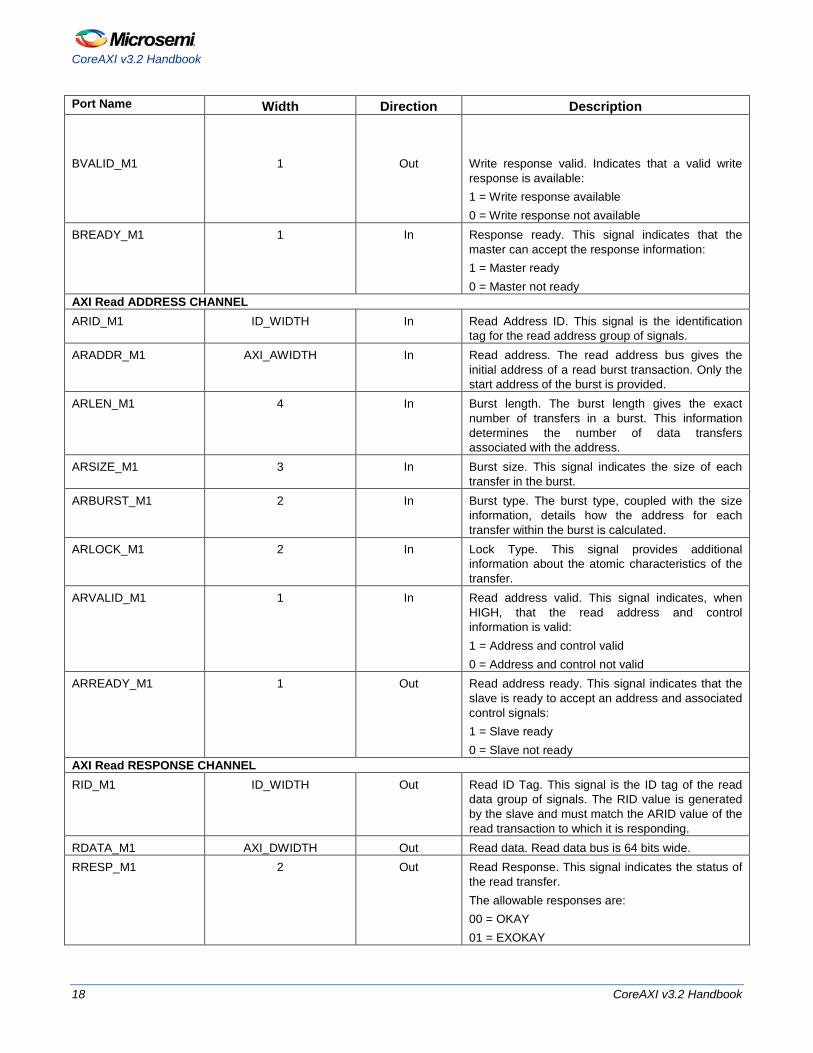
I/O Signal descriptions for CoreAXI are defined in Table 3.
Table 3 I/O Signals Port Name Width Direction Description Global Signal Ports ACLK 1 In AXI clock. All the AXI signals inside the block are
clocked on the rising edge. ARESETN 1 In AXI reset signal. The signal is active low.
Asynchronous assertion and synchronous de-assertion. This is used to reset all the AXI registers in the Block.
AXI Master 0 Interface Ports AXI Write ADDRESS CHANNEL AWID_M0 ID_WIDTH In Write Address ID. This Signal is the Identification
tag for the write address group of signals. AWADDR_M0 AXI_AWIDTH In Write address. The write address bus gives the
address of the first transfer in a write burst. The associated control signals are used to determine the addresses of the remaining transfers in the burst.
AWLEN_M0 4 In Burst length. The burst length gives the exact number of transfers in a burst. This information determines the number of data transfers associated with the address.
AWSIZE_M0 3 In Burst size. This signal indicates the size of each transfer in the burst.
AWBURST_M0 2 In Burst type. The burst type, coupled with the size information, details how the address for each transfer within the burst is calculated.
AWLOCK_M0 2 In Lock type. This signal provides additional information about the atomic characteristics of the transfer.
AWVALID_M0 1 In Write address valid. This signal indicates that valid write address and control information are available: 1 = Address and control available 0 = Address and control not available
AWREADY_M0 1 Out Write address ready. This signal indicates that the slave is ready to accept an address and associated control signals: 1 = Slave ready 0 = Slave not ready
AXI Write DATA CHANNEL WID_M0 ID_WIDTH In Write Data ID tag. This is the Identification tag for
the write data transfer. The WID must match the AWID value of the write transaction.
WDATA_M0 AXI_DWIDTH In Write data bus is 64 bits wide.

Place-and-Route in Libero SoC
CoreAXI v3.2 Handbook 15
Port Name Width Direction Description WSTRB_M0
8
In
Write strobes. This signal indicates which byte lanes to update in memory. There is one write strobe for each eight bits of the write data bus. WSTRB[n] corresponds to WDATA [(8 × n) + 7 :( 8 × n)].
WLAST_M0 1 In Write last. This signal indicates the last transfer in a write burst.
WVALID_M0 1 In Write valid. Indicates that valid write data and strobes are available: 1 = Write data and strobes available 0 = Write data and strobes unavailable
WREADY_M0 1 Out Write ready. This indicates that the slave can accept the write data: 1 = Slave ready 0 = Slave not ready
AXI Write RESPONSE CHANNEL BID_M0 ID_WIDTH Out Response ID. This is the Identification tag for the
write response. The BID must match the AWID value of the write transaction to which the slave is responding.
BRESP_M0 2 Out Write response. This signal indicates the status of the write transaction. The allowable responses are: 00 = OKAY 01 = EXOKAY 10 = SLVERR DECERR is not supported.
BVALID_M0 1 Out Write response valid. Indicates that a valid write response is available: 1 = Write response available 0 = Write response not available
BREADY_M0 1 In Response ready. This signal indicates that the master can accept the response information: 1 = Master ready 0 = Master not ready
AXI Read ADDRESS CHANNEL ARID_M0 ID_WIDTH In Read Address ID. This signal is the identification
tag for the read address group of signals. ARADDR_M0 AXI_AWIDTH In Read address. The read address bus gives the
initial address of a read burst transaction. Only the start address of the burst is provided.
ARLEN_M0 4 In Burst length. The burst length gives the exact number of transfers in a burst. This information determines the number of data transfers associated with the address.
ARSIZE_M0 3 In Burst size. This signal indicates the size of each transfer in the burst.
ARBURST_M0 2 In Burst type. The burst type, coupled with the size information, details how the address for each

CoreAXI v3.2 Handbook
16 CoreAXI v3.2 Handbook
Port Name Width Direction Description transfer within the burst is calculated.
ARLOCK_M0 2 In Lock Type. This signal provides additional information about the atomic characteristics of the transfer.
ARVALID_M0 1 In Read address valid. This signal indicates, when HIGH, that the read address and control information is valid: 1 = Address and control valid 0 = Address and control not valid
ARREADY_M0 1 Out Read address ready. This signal indicates that the slave is ready to accept an address and associated control signals: 1 = Slave ready 0 = Slave not ready
AXI Read RESPONSE CHANNEL RID_M0 ID_WIDTH Out Read ID Tag. This signal is the ID tag of the read
data group of signals. The RID value is generated by the slave and must match the ARID value of the read transaction to which it is responding.
RDATA_M0 AXI_DWIDTH Out Read data. Read data bus is 64 bits wide. RRESP_M0 2 Out Read Response. This signal indicates the status of
the read transfer. The allowable responses are: 00 = OKAY 01 = EXOKAY 10 = SLVERR DECERR is not supported.
RLAST_M0 1 Out Read Last. This signal indicates the last transfer in a read burst.
RVALID_M0 1 Out Read Valid. This signal indicates that the required read data is available and the read transfer can complete: 1 = Read data available 0 = Read data not available
RREADY_M0 1 In Read ready. This signal indicates that the master can accept the read data and response information: 1 = Master ready 0 = Master not ready
AXI Master 1 Interface Ports AXI Write ADDRESS CHANNEL AWID_M1 ID_WIDTH In Write Address ID. This Signal is the Identification
tag for the write address group of signals. AWADDR_M1 AXI_AWIDTH In Write address. The write address bus gives the
address of the first transfer in a write burst. The associated control signals are used to determine the addresses of the remaining transfers in the burst.
AWLEN_M1 4 In Burst length. The burst length gives the exact number of transfers in a burst. This information

Place-and-Route in Libero SoC
CoreAXI v3.2 Handbook 17
Port Name Width Direction Description determines the number of data transfers associated with the address.
AWSIZE_M1 3 In Burst size. This signal indicates the size of each transfer in the burst.
AWBURST_M1 2 In Burst type. The burst type, coupled with the size information, details how the address for each transfer within the burst is calculated.
AWLOCK_M1 2 In Lock type. This signal provides additional information about the atomic characteristics of the transfer.
AWVALID_M1 1 In Write address valid. This signal indicates that valid write address and control information are available: 1 = Address and control available 0 = Address and control not available
AWREADY_M1 1 Out Write address ready. This signal indicates that the slave is ready to accept an address and associated control signals: 1 = Slave ready 0 = Slave not ready
AXI Write DATA CHANNEL WID_M1 ID_WIDTH In Write Data ID tag. This is the Identification tag for
the write data transfer. The WID must match the AWID value of the write transaction.
WDATA_M1 AXI_DWIDTH In Write data bus is 64 bits wide. WSTRB_M1 8 In Write strobes. This signal indicates which byte
lanes to update in memory. There is one write strobe for each eight bits of the write data bus. WSTRB[n] corresponds to WDATA [(8 × n) + 7 :( 8 × n)].
WLAST_M1 1 In Write last. This signal indicates the last transfer in a write burst.
WVALID_M1 1 In Write valid. Indicates that valid write data and strobes are available: 1 = Write data and strobes available 0 = Write data and strobes unavailable
WREADY_M1 1 Out Write ready. This indicates that the slave can accept the write data: 1 = Slave ready 0 = Slave not ready
AXI Write RESPONSE CHANNEL BID_M1 ID_WIDTH Out Response ID. This is the Identification tag for the
write response. The BID must match the AWID value of the write transaction to which the slave is responding.
BRESP_M1 2 Out Write response. This signal indicates the status of the write transaction. The allowable responses are: 00 = OKAY 01 = EXOKAY 10 = SLVERR DECERR is not supported.
CoreAXI v3.2 Handbook
18 CoreAXI v3.2 Handbook
Port Name Width Direction Description BVALID_M1
1
Out
Write response valid. Indicates that a valid write response is available: 1 = Write response available 0 = Write response not available
BREADY_M1 1 In Response ready. This signal indicates that the master can accept the response information: 1 = Master ready 0 = Master not ready
AXI Read ADDRESS CHANNEL ARID_M1 ID_WIDTH In Read Address ID. This signal is the identification
tag for the read address group of signals. ARADDR_M1 AXI_AWIDTH In Read address. The read address bus gives the
initial address of a read burst transaction. Only the start address of the burst is provided.
ARLEN_M1 4 In Burst length. The burst length gives the exact number of transfers in a burst. This information determines the number of data transfers associated with the address.
ARSIZE_M1 3 In Burst size. This signal indicates the size of each transfer in the burst.
ARBURST_M1 2 In Burst type. The burst type, coupled with the size information, details how the address for each transfer within the burst is calculated.
ARLOCK_M1 2 In Lock Type. This signal provides additional information about the atomic characteristics of the transfer.
ARVALID_M1 1 In Read address valid. This signal indicates, when HIGH, that the read address and control information is valid: 1 = Address and control valid 0 = Address and control not valid
ARREADY_M1 1 Out Read address ready. This signal indicates that the slave is ready to accept an address and associated control signals: 1 = Slave ready 0 = Slave not ready
AXI Read RESPONSE CHANNEL RID_M1 ID_WIDTH Out Read ID Tag. This signal is the ID tag of the read
data group of signals. The RID value is generated by the slave and must match the ARID value of the read transaction to which it is responding.
RDATA_M1 AXI_DWIDTH Out Read data. Read data bus is 64 bits wide. RRESP_M1 2 Out Read Response. This signal indicates the status of
the read transfer. The allowable responses are: 00 = OKAY 01 = EXOKAY

Place-and-Route in Libero SoC
CoreAXI v3.2 Handbook 19
Port Name Width Direction Description 10 = SLVERR DECERR is not supported.
RLAST_M1 1 Out Read Last. This signal indicates the last transfer in a read burst.
RVALID_M1 1 Out Read Valid. This signal indicates that the required read data is available and the read transfer can complete: 1 = Read data available 0 = Read data not available
RREADY_M1 1 In Read ready. This signal indicates that the master can accept the read data and response information: 1 = Master ready 0 = Master not ready
AXI Master 2 Interface Ports AXI Write ADDRESS CHANNEL AWID_M2 ID_WIDTH In Write Address ID. This Signal is the Identification
tag for the write address group of signals. AWADDR_M2 AXI_AWIDTH In Write address. The write address bus gives the
address of the first transfer in a write burst. The associated control signals are used to determine the addresses of the remaining transfers in the burst.
AWLEN_M2 4 In Burst length. The burst length gives the exact number of transfers in a burst. This information determines the number of data transfers associated with the address.
AWSIZE_M2 3 In Burst size. This signal indicates the size of each transfer in the burst.
AWBURST_M2 2 In Burst type. The burst type, coupled with the size information, details how the address for each transfer within the burst is calculated.
AWLOCK_M2 2 In Lock type. This signal provides additional information about the atomic characteristics of the transfer.
AWVALID_M2 1 In Write address valid. This signal indicates that valid write address and control information are available: 1 = Address and control available 0 = Address and control not available
AWREADY_M2 1 Out Write address ready. This signal indicates that the slave is ready to accept an address and associated control signals: 1 = Slave ready 0 = Slave not ready
AXI Write DATA CHANNEL WID_M2 ID_WIDTH In Write Data ID tag. This is the Identification tag for
the write data transfer. The WID must match the AWID value of the write transaction.
WDATA_M2 AXI_DWIDTH In Write data bus is 64 bits wide. WSTRB_M2 8 In Write strobes. This signal indicates which byte

CoreAXI v3.2 Handbook
20 CoreAXI v3.2 Handbook
Port Name Width Direction Description lanes to update in memory. There is one write strobe for each eight bits of the write data bus. WSTRB[n] corresponds to WDATA [(8 × n) + 7 :( 8 × n)].
WLAST_M2 1 In Write last. This signal indicates the last transfer in a write burst.
WVALID_M2 1 In Write valid. Indicates that valid write data and strobes are available: 1 = Write data and strobes available 0 = Write data and strobes unavailable
WREADY_M2 1 Out Write ready. This indicates that the slave can accept the write data: 1 = Slave ready 0 = Slave not ready
AXI Write RESPONSE CHANNEL BID_M2 ID_WIDTH Out Response ID. This is the Identification tag for the
write response. The BID must match the AWID value of the write transaction to which the slave is responding.
BRESP_M2 2 Out Write response. This signal indicates the status of the write transaction. The allowable responses are: 00 = OKAY 01 = EXOKAY 10 = SLVERR DECERR is not supported.
BVALID_M2 1 Out Write response valid. Indicates that a valid write response is available: 1 = Write response available 0 = Write response not available
BREADY_M2 1 In Response ready. This signal indicates that the master can accept the response information: 1 = Master ready 0 = Master not ready
AXI Read ADDRESS CHANNEL ARID_M2 ID_WIDTH In Read Address ID. This signal is the identification
tag for the read address group of signals. ARADDR_M2 AXI_AWIDTH In Read address. The read address bus gives the
initial address of a read burst transaction. Only the start address of the burst is provided.
ARLEN_M2 4 In Burst length. The burst length gives the exact number of transfers in a burst. This information determines the number of data transfers associated with the address.
ARSIZE_M2 3 In Burst size. This signal indicates the size of each transfer in the burst.
ARBURST_M2 2 In Burst type. The burst type, coupled with the size information, details how the address for each transfer within the burst is calculated.
ARLOCK_M2 2 In Lock Type. This signal provides additional information about the atomic characteristics of the

Place-and-Route in Libero SoC
CoreAXI v3.2 Handbook 21
Port Name Width Direction Description transfer.
ARVALID_M2 1 In Read address valid. This signal indicates, when HIGH, that the read address and control information is valid: 1 = Address and control valid 0 = Address and control not valid
ARREADY_M2 1 Out Read address ready. This signal indicates that the slave is ready to accept an address and associated control signals: 1 = Slave ready 0 = Slave not ready
AXI Read RESPONSE CHANNEL RID_M2 ID_WIDTH Out Read ID Tag. This signal is the ID tag of the read
data group of signals. The RID value is generated by the slave and must match the ARID value of the read transaction to which it is responding.
RDATA_M2 AXI_DWIDTH Out Read data. Read data bus is 64 bits wide. RRESP_M2 2 Out Read Response. This signal indicates the status of
the read transfer. The allowable responses are: 00 = OKAY 01 = EXOKAY 10 = SLVERR DECERR is not supported.
RLAST_M2 1 Out Read Last. This signal indicates the last transfer in a read burst.
RVALID_M2 1 Out Read Valid. This signal indicates that the required read data is available and the read transfer can complete: 1 = Read data available 0 = Read data not available
RREADY_M2 1 In Read ready. This signal indicates that the master can accept the read data and response information: 1 = Master ready 0 = Master not ready
AXI Master 3 Interface Ports AXI Write ADDRESS CHANNEL AWID_M3 ID_WIDTH In Write Address ID. This Signal is the Identification
tag for the write address group of signals. AWADDR_M3 AXI_AWIDTH In Write address. The write address bus gives the
address of the first transfer in a write burst. The associated control signals are used to determine the addresses of the remaining transfers in the burst.
AWLEN_M3 4 In Burst length. The burst length gives the exact number of transfers in a burst. This information determines the number of data transfers associated with the address.
AWSIZE_M3 3 In Burst size. This signal indicates the size of each

CoreAXI v3.2 Handbook
22 CoreAXI v3.2 Handbook
Port Name Width Direction Description transfer in the burst.
AWBURST_M3 2 In Burst type. The burst type, coupled with the size information, details how the address for each transfer within the burst is calculated.
AWLOCK_M3 2 In Lock type. This signal provides additional information about the atomic characteristics of the transfer.
AWVALID_M3 1 In Write address valid. This signal indicates that valid write address and control information are available: 1 = Address and control available 0 = Address and control not available
AWREADY_M3 1 Out Write address ready. This signal indicates that the slave is ready to accept an address and associated control signals: 1 = Slave ready 0 = Slave not ready
AXI Write DATA CHANNEL WID_M3 ID_WIDTH In Write Data ID tag. This is the Identification tag for
the write data transfer. The WID must match the AWID value of the write transaction.
WDATA_M3 AXI_DWIDTH In Write data bus is 64 bits wide. WSTRB_M3 8 In Write strobes. This signal indicates which byte
lanes to update in memory. There is one write strobe for each eight bits of the write data bus. WSTRB[n] corresponds to WDATA [(8 × n) + 7 :( 8 × n)].
WLAST_M3 1 In Write last. This signal indicates the last transfer in a write burst.
WVALID_M3 1 In Write valid. Indicates that valid write data and strobes are available: 1 = Write data and strobes available 0 = Write data and strobes unavailable
WREADY_M3 1 Out Write ready. This indicates that the slave can accept the write data: 1 = Slave ready 0 = Slave not ready
AXI Write RESPONSE CHANNEL BID_M3 ID_WIDTH Out Response ID. This is the Identification tag for the
write response. The BID must match the AWID value of the write transaction to which the slave is responding.
BRESP_M3 2 Out Write response. This signal indicates the status of the write transaction. The allowable responses are: 00 = OKAY 01 = EXOKAY 10 = SLVERR DECERR is not supported.
BVALID_M3 1 Out Write response valid. Indicates that a valid write

Place-and-Route in Libero SoC
CoreAXI v3.2 Handbook 23
Port Name Width Direction Description response is available: 1 = Write response available 0 = Write response not available
BREADY_M3 1 In Response ready. This signal indicates that the master can accept the response information: 1 = Master ready 0 = Master not ready
AXI Read ADDRESS CHANNEL ARID_M3 ID_WIDTH In Read Address ID. This signal is the identification
tag for the read address group of signals. ARADDR_M3 AXI_AWIDTH In Read address. The read address bus gives the
initial address of a read burst transaction. Only the start address of the burst is provided.
ARLEN_M3 4 In Burst length. The burst length gives the exact number of transfers in a burst. This information determines the number of data transfers associated with the address.
ARSIZE_M3 3 In Burst size. This signal indicates the size of each transfer in the burst.
ARBURST_M3 2 In Burst type. The burst type, coupled with the size information, details how the address for each transfer within the burst is calculated.
ARLOCK_M3 2 In Lock Type. This signal provides additional information about the atomic characteristics of the transfer.
ARVALID_M3 1 In Read address valid. This signal indicates, when HIGH, that the read address and control information is valid: 1 = Address and control valid 0 = Address and control not valid
ARREADY_M3 1 Out Read address ready. This signal indicates that the slave is ready to accept an address and associated control signals: 1 = Slave ready 0 = Slave not ready
AXI Read RESPONSE CHANNEL RID_M3 ID_WIDTH Out Read ID Tag. This signal is the ID tag of the read
data group of signals. The RID value is generated by the slave and must match the ARID value of the read transaction to which it is responding.
RDATA_M3 AXI_DWIDTH Out Read data. Read data bus is 64 bits wide. RRESP_M3 2 Out Read Response. This signal indicates the status of
the read transfer. The allowable responses are: 00 = OKAY 01 = EXOKAY 10 = SLVERR DECERR is not supported.
RLAST_M3 1 Out Read Last. This signal indicates the last transfer in

CoreAXI v3.2 Handbook
24 CoreAXI v3.2 Handbook
Port Name Width Direction Description a read burst.
RVALID_M3 1 Out Read Valid. This signal indicates that the required read data is available and the read transfer can complete: 1 = Read data available 0 = Read data not available
RREADY_M3
1
In
Read ready. This signal indicates that the master can accept the read data and response information: 1= Master ready 0 = Master not ready
AXI Slave 0 Interface Ports AXI Write ADDRESS CHANNEL AWID_S0 ID_WIDTH + 2 Out Write Address ID. This Signal is the Identification
tag for the write address group of signals. AWADDR_S0 AXI_AWIDTH Out Write address. The write address bus gives the
address of the first transfer in a write burst. The associated control signals are used to determine the addresses of the remaining transfers in the burst.
AWLEN_S0 4 Out Burst length. The burst length gives the exact number of transfers in a burst. This information determines the number of data transfers associated with the address.
AWSIZE_S0 3 Out Burst size. This signal indicates the size of each transfer in the burst.
AWBURST_S0 2 Out Burst type. The burst type, coupled with the size information, details how the address for each transfer within the burst is calculated.
AWLOCK_S0 2 Out Lock type. This signal provides additional information about the atomic characteristics of the transfer.
AWVALID_S0 1 Out Write address valid. This signal indicates that valid write address and control information are available: 1 = Address and control available 0 = Address and control not available
AWREADY_S0 1 In Write address ready. This signal indicates that the slave is ready to accept an address and associated control signals: 1 = Slave ready 0 = Slave not ready
AXI Write DATA CHANNEL WID_S0 ID_WIDTH + 2 Out Write Data ID tag. This is the Identification tag for
the write data transfer. The WID must match the AWID value of the write transaction.
WDATA_S0 AXI_DWIDTH Out Write data bus is 64 bits wide. WSTRB_S0 8 Out Write strobes. This signal indicates which byte

Place-and-Route in Libero SoC
CoreAXI v3.2 Handbook 25
Port Name Width Direction Description lanes to update in memory. There is one write strobe for each eight bits of the write data bus. WSTRB[n] corresponds to WDATA [(8 × n) + 7 :( 8 × n)].
WLAST_S0 1 Out Write last. This signal indicates the last transfer in a write burst.
WVALID_S0 1 Out Write valid. Indicates that valid write data and strobes are available: 1 = Write data and strobes available 0 = Write data and strobes unavailable
WREADY_S0
1
In
Write ready. This indicates that the slave can accept the write data: 1 = Slave ready 0 = Slave not ready
AXI Write RESPONSE CHANNEL BID_S0 ID_WIDTH + 2 In Response ID. This is the Identification tag for the
write response. The BID must match the AWID value of the write transaction to which the slave is responding.
BRESP_S0 2 In Write response. This signal indicates the status of the write transaction. The allowable responses are: 00 = OKAY 01 = EXOKAY 10 = SLVERR DECERR is not supported.
BVALID_S0 1 In Write response valid. Indicates that a valid write response is available: 1 = Write response available 0 = Write response not available
BREADY_S0 1 Out Response ready. This signal indicates that the master can accept the response information: 1 = Master ready 0 = Master not ready
AXI Read ADDRESS CHANNEL ARID_S0 ID_WIDTH + 2 Out Read Address ID. This signal is the identification
tag for the read address group of signals. ARADDR_S0 AXI_AWIDTH Out Read address. The read address bus gives the
initial address of a read burst transaction. Only the start address of the burst is provided.
ARLEN_S0 4 Out Burst length. The burst length gives the exact number of transfers in a burst. This information determines the number of data transfers associated with the address.
ARSIZE_S0 3 Out Burst size. This signal indicates the size of each transfer in the burst.
ARBURST_S0 2 Out Burst type. The burst type, coupled with the size information, details how the address for each transfer within the burst is calculated.

CoreAXI v3.2 Handbook
26 CoreAXI v3.2 Handbook
Port Name Width Direction Description ARLOCK_S0 2 Out Lock Type. This signal provides additional
information about the atomic characteristics of the transfer.
ARVALID_S0 1 Out Read address valid. This signal indicates, when HIGH, that the read address and control information is valid: 1 = Address and control valid 0 = Address and control not valid
ARREADY_S0 1 In Read address ready. This signal indicates that the slave is ready to accept an address and associated control signals: 1 = Slave ready 0 = Slave not ready
AXI Read RESPONSE CHANNEL RID_S0 ID_WIDTH + 2 In Read ID Tag. This signal is the ID tag of the read
data group of signals. The RID value is generated by the slave and must match the ARID value of the read transaction to which it is responding.
RDATA_S0 AXI_DWIDTH In Read data. Read data bus is 64 bits wide. RRESP_S0 2 In Read Response. This signal indicates the status of
the read transfer. The allowable responses are: 00 = OKAY 01 = EXOKAY 10 = SLVERR DECERR is not supported.
RLAST_S0 1 In Read Last. This signal indicates the last transfer in a read burst.
RVALID_S0 1 In Read Valid. This signal indicates that the required read data is available and the read transfer can complete: 1 = Read data available 0 = Read data not available
RREADY_S0 1 Out Read ready. This signal indicates that the master can accept the read data and response information: 1 = Master ready 0 = Master not ready
AXI Slave 15 Interface Ports AXI Write ADDRESS CHANNEL AWID_S15 ID_WIDTH + 2 Out Write Address ID. This Signal is the Identification
tag for the write address group of signals. AWADDR_S15 AXI_AWIDTH Out Write address. The write address bus gives the
address of the first transfer in a write burst. The associated control signals are used to determine the addresses of the remaining transfers in the burst.
AWLEN_S15 4 Out Burst length. The burst length gives the exact number of transfers in a burst. This information determines the number of data transfers

Place-and-Route in Libero SoC
CoreAXI v3.2 Handbook 27
Port Name Width Direction Description associated with the address.
AWSIZE_S15 3 Out Burst size. This signal indicates the size of each transfer in the burst.
AWBURST_S15 2 Out Burst type. The burst type, coupled with the size information, details how the address for each transfer within the burst is calculated.
AWLOCK_S15 2 Out Lock type. This signal provides additional information about the atomic characteristics of the transfer.
AWVALID_S15 1 Out Write address valid. This signal indicates that valid write address and control information are available: 1 = Address and control available 0 = Address and control not available
AWREADY_S15
1
In
Write address ready. This signal indicates that the slave is ready to accept an address and associated control signals: 1 = Slave ready 0 = Slave not ready
AXI Write DATA CHANNEL WID_S15 ID_WIDTH + 2 Out Write Data ID tag. This is the Identification tag for
the write data transfer. The WID must match the AWID value of the write transaction.
WDATA_S15 AXI_DWIDTH Out Write data bus is 64 bits wide. WSTRB_S15 8 Out Write strobes. This signal indicates which byte
lanes to update in memory. There is one write strobe for each eight bits of the write data bus. WSTRB[n] corresponds to WDATA [(8 × n) + 7 :( 8 × n)].
WLAST_S15 1 Out Write last. This signal indicates the last transfer in a write burst.
WVALID_S15 1 Out Write valid. Indicates that valid write data and strobes are available: 1 = Write data and strobes available 0 = Write data and strobes unavailable
WREADY_S15 1 In Write ready. This indicates that the slave can accept the write data: 1 = Slave ready 0 = Slave not ready
AXI Write RESPONSE CHANNEL BID_S15 ID_WIDTH + 2 In Response ID. This is the Identification tag for the
write response. The BID must match the AWID value of the write transaction to which the slave is responding.
BRESP_S15 2 In Write response. This signal indicates the status of the write transaction. The allowable responses are: 00 = OKAY 01 = EXOKAY 10 = SLVERR

CoreAXI v3.2 Handbook
28 CoreAXI v3.2 Handbook
Port Name Width Direction Description DECERR is not supported.
BVALID_S15 1 In Write response valid. Indicates that a valid write response is available: 1 = Write response available 0 = Write response not available
BREADY_S15 1 Out Response ready. This signal indicates that the master can accept the response information: 1 = Master ready 0 = Master not ready
AXI Read ADDRESS CHANNEL ARID_S15 ID_WIDTH + 2 Out Read Address ID. This signal is the identification
tag for the read address group of signals. ARADDR_S15 AXI_AWIDTH Out Read address. The read address bus gives the
initial address of a read burst transaction. Only the start address of the burst is provided.
ARLEN_S15 4 Out Burst length. The burst length gives the exact number of transfers in a burst. This information determines the number of data transfers associated with the address.
ARSIZE_S15 3 Out Burst size. This signal indicates the size of each transfer in the burst.
ARBURST_S15 2 Out Burst type. The burst type, coupled with the size information, details how the address for each transfer within the burst is calculated.
ARLOCK_S15 2 Out Lock Type. This signal provides additional information about the atomic characteristics of the transfer.
ARVALID_S15 1 Out Read address valid. This signal indicates, when HIGH, that the read address and control information is valid: 1 = Address and control valid 0 = Address and control not valid
ARREADY_S15 1 In Read address ready. This signal indicates that the slave is ready to accept an address and associated control signals: 1 = Slave ready 0 = Slave not ready
AXI Read RESPONSE CHANNEL RID_S15 ID_WIDTH + 2 In Read ID Tag. This signal is the ID tag of the read
data group of signals. The RID value is generated by the slave and must match the ARID value of the read transaction to which it is responding.
RDATA_S15 AXI_DWIDTH In Read data. Read data bus is 64 bits wide. RRESP_S15 2 In Read Response. This signal indicates the status of
the read transfer. The allowable responses are: 00 = OKAY 01 = EXOKAY 10 = SLVERR

Place-and-Route in Libero SoC
CoreAXI v3.2 Handbook 29
Port Name Width Direction Description DECERR is not supported.
RLAST_S15 1 In Read Last. This signal indicates the last transfer in a read burst.
RVALID_S15 1 In Read Valid. This signal indicates that the required read data is available and the read transfer can complete: 1 = Read data available 0 = Read data not available
RREADY_S15 1 Out Read ready. This signal indicates that the master can accept the read data and response information: 1 = Master ready 0 = Master not ready
AXI Slave 16 Interface Ports (Valid only if huge slot or combined region is used) AXI Write ADDRESS CHANNEL AWID_S16
ID_WIDTH + 2
Out
Write Address ID. This Signal is the Identification tag for the write address group of signals.
AWADDR_S16 AXI_AWIDTH Out Write address. The write address bus gives the address of the first transfer in a write burst. The associated control signals are used to determine the addresses of the remaining transfers in the burst.
AWLEN_S16 4 Out Burst length. The burst length gives the exact number of transfers in a burst. This information determines the number of data transfers associated with the address.
AWSIZE_S16 3 Out Burst size. This signal indicates the size of each transfer in the burst.
AWBURST_S16 2 Out Burst type. The burst type, coupled with the size information, details how the address for each transfer within the burst is calculated.
AWLOCK_S16 2 Out Lock type. This signal provides additional information about the atomic characteristics of the transfer.
AWVALID_S16 1 Out Write address valid. This signal indicates that valid write address and control information are available: 1 = Address and control available 0 = Address and control not available
AWREADY_S16 1 In Write address ready. This signal indicates that the slave is ready to accept an address and associated control signals: 1 = Slave ready 0 = Slave not ready
AXI Write DATA CHANNEL WID_S16 ID_WIDTH + 2 Out Write Data ID tag. This is the Identification tag for
the write data transfer. The WID must match the AWID value of the write transaction.
WDATA_S16 AXI_DWIDTH Out Write data bus is 64 bits wide.

CoreAXI v3.2 Handbook
30 CoreAXI v3.2 Handbook
Port Name Width Direction Description WSTRB_S16 8 Out Write strobes. This signal indicates which byte
lanes to update in memory. There is one write strobe for each eight bits of the write data bus. WSTRB[n] corresponds to WDATA [(8 × n) + 7 :( 8 × n)].
WLAST_S16 1 Out Write last. This signal indicates the last transfer in a write burst.
WVALID_S16 1 Out Write valid. Indicates that valid write data and strobes are available: 1 = Write data and strobes available 0 = Write data and strobes unavailable
WREADY_S16 1 In Write ready. This indicates that the slave can accept the write data: 1 = Slave ready 0 = Slave not ready
AXI Write RESPONSE CHANNEL BID_S16
ID_WIDTH + 2
In
Response ID. This is the Identification tag for the write response. The BID must match the AWID value of the write transaction to which the slave is responding.
BRESP_S16 2 In Write response. This signal indicates the status of the write transaction. The allowable responses are: 00 = OKAY 01 = EXOKAY 10 = SLVERR DECERR is not supported.
BVALID_S16 1 In Write response valid. Indicates that a valid write response is available: 1 = Write response available 0 = Write response not available
BREADY_S16 1 Out Response ready. This signal indicates that the master can accept the response information. 1 = Master ready 0 = Master not ready
AXI Read ADDRESS CHANNEL ARID_S16 ID_WIDTH + 2 Out Read Address ID. This signal is the identification
tag for the read address group of signals. ARADDR_S16 AXI_AWIDTH Out Read address. The read address bus gives the
initial address of a read burst transaction. Only the start address of the burst is provided.
ARLEN_S16 4 Out Burst length. The burst length gives the exact number of transfers in a burst. This information determines the number of data transfers associated with the address.
ARSIZE_S16 3 Out Burst size. This signal indicates the size of each transfer in the burst.
ARBURST_S16 2 Out Burst type. The burst type, coupled with the size

Place-and-Route in Libero SoC
CoreAXI v3.2 Handbook 31
Port Name Width Direction Description information, details how the address for each transfer within the burst is calculated.
ARLOCK_S16 2 Out Lock Type. This signal provides additional information about the atomic characteristics of the transfer.
ARVALID_S16 1 Out Read address valid. This signal indicates, when HIGH, that the read address and control information is valid: 1 = Address and control valid 0 = Address and control not valid
ARREADY_S16 1 In Read address ready. This signal indicates that the slave is ready to accept an address and associated control signals: 1 = Slave ready 0 = Slave not ready
AXI Read RESPONSE CHANNEL RID_S16 ID_WIDTH + 2 In Read ID Tag. This signal is the ID tag of the read
data group of signals. The RID value is generated by the slave and must match the ARID value of the read transaction to which it is responding.
RDATA_S16 AXI_DWIDTH In Read data. Read data bus is 64 bits wide. RRESP_S16 2 In Read Response. This signal indicates the status of
the read transfer. The allowable responses are: 00 = OKAY 01 = EXOKAY 10 = SLVERR DECERR is not supported.
RLAST_S16 1 In Read Last. This signal indicates the last transfer in a read burst.
RVALID_S16 1 In Read Valid. This signal indicates that the required read data is available and the read transfer can complete: 1 = Read data available 0 = Read data not available
RREADY_S16 1 Out Read ready. This signal indicates that the master can accept the read data and response information: 1= Master ready 0 = Master not ready

CoreAXI v3.2 Handbook
32 CoreAXI v3.2 Handbook
Core Parameters There are a number of configurable options that apply to CoreAXI as shown in Table 4. If a configuration other than the default is required, use the configuration dialog box in SmartDesign to select appropriate values for the configurable options.
Table 4 CoreAXI Configuration Options Name Valid Range Default Description
FAMILY 19, 24, 25 19 Must be set to the required FPGA family: 19= SmartFusion2 24= IGLOO2 25= RTG4
AXI_AWIDTH 32 32 A 32-bit System AXI address bus. AXI_DWIDTH 64,128, 256 64 Write/Read data bus on AXI side. NUM_MASTER_SLOT 1-4 1 Select number of master slots to be
connected. ID_WIDTH 4 4 Width of ID field for all AXI channels.
Note: ID_WIDTH is fixed to four.
MEMSPACE 0-6 1 0= 1 huge slave slot of 2 GB and the other 2 GB addressable space is apportioned into remaining 8 slave slots of either 4 KB, 64 KB, 1 MB, 16 MB or 256 MB using HGS_CFG 1= 4 GB addressable space apportioned into 16 slave slots each of 256 MB 2= 256 MB addressable space apportioned into 16 slave slots each of 16 MB 3= 16 MB addressable space apportioned into 16 slave slots each of 1MB 4= 1 MB addressable space apportioned into 16 slave slots each of 64 KB 5= 64 KB addressable space apportioned into 16 slave slots each of 4 KB 6= 4 KB addressable space apportioned into 16 slave slots each of 256 bytes
HGS_CFG 1-6 1 1 = 2 GB addressable space apportioned into 8 slave slots each of 256MB 2 = 256 MB addressable space apportioned into 8 slave slots each of 16 MB 3 = 16 MB addressable space apportioned into 8 slave slots each of 1 MB 4 = 1 MB addressable space apportioned into 8 slave slots each of 64 KB 5 = 64 KB addressable space apportioned into 8 slave slots each of 4 KB 6 = 4 KB addressable space apportioned into 8 slave slots each of 256 Bytes Note: This is relevant only when

Core Parameters
CoreAXI v3.2 Handbook 33
Name Valid Range Default Description
MEMSPACE = 0.
ADDR_HGS_CFG 0-1 1 0 = AXI address [31] tied low, huge slave address range is 0x00000000 to 0x7FFFFFFF 1 = AXI address [31] tied high, huge slave address range is 0x80000000 to 0xFFFFFFFF Note: This is relevant only when
MEMSPACE = 0.
SC_0 0 or 1 0 This parameter is relevant only when MEMSPACE > 0. It is used to assign slave slot 0 to the combined region. 0 = Slave slot 0 is not assigned to the combined region. Slave interface 0 is available for connection, if enabled. 1 = Slave slot 0 is assigned to the combined region. Slave interface 16 is available for connection, if enabled but slave interface 0 is not available for connection.
SC_1 0 or 1 0 This parameter is relevant only when MEMSPACE > 0. It is used to assign slave slot 1 to the combined region. 0 = Slave slot 1 is not assigned to the combined region. Slave interface 1 is available for connection, if enabled. 1 = Slave slot 1 is assigned to the combined region. Slave interface 16 is available for connection, if enabled but slave interface 1 is not available for connection.
... ... ... SC_15 0 or 1 0 This parameter is relevant only when
MEMSPACE > 0. It is used to assign slave slot 15 to the combined region. 0 = Slave slot 15 is not assigned to the combined region. Slave interface 15 is available for connection, if enabled. 1 = Slave slot 15 is assigned to the combined region. Slave interface 16 is available for connection, if enabled but slave interface 15 is not available for connection.
MASTER0SLAVE0ENABLE 0 or 1 1 Enables or disables slave0 for master 0 0 = Disable slave0 for master 0 1 = Enable slave0 for master 0 When ADDR_HGS_CFG = 0 and

CoreAXI v3.2 Handbook
34 CoreAXI v3.2 Handbook
Name Valid Range Default Description
MEMSPACE=0, MASTER0SLAVE0ENABLE is not relevant and slave0 is not available for connection.
MASTER0SLAVE1ENABLE 0 or 1 0 Enables or disables slave 1 for master 0 0 = Disable slave1 for master 0 1 = Enable slave1 for master 0 When ADDR_HGS_CFG = 0 and MEMSPACE=0, MASTER0SLAVE1ENABLE is not relevant and slave1 is not available for connection.
... … ... MASTER0SLAVE15ENABLE 0 or 1 0 Enables or disables slave15 for master 0
0 = Disable slave15 for master 0 1 = Enable slave15 for master 0 When ADDR_HGS_CFG = 1 and MEMSPACE=0, MASTER0SLAVE15ENABLE is not relevant and slave15 is not available for connection.
MASTER0SLAVE16ENABLE 0 or 1 0 Enables or disables slave16 for master 0 0 = Disable slave16 for master 0 1 = Enable slave16 for master 0 When ADDR_HGS_CFG = 1 and MEMSPACE=0, MASTER0SLAVE16ENABLE is not relevant and slave16 is not available for connection.
MASTER1SLAVE0ENABLE 0 or 1 0 Enables or disables slave0 for master 1 0 = Disable slave0 for master 1 1 = Enable slave0 for master 1 When ADDR_HGS_CFG = 0 and MEMSPACE=0, MASTER1SLAVE0ENABLE is not relevant and slave0 is not available for connection.
MASTER1SLAVE1ENABLE 0 or 1 0 Enables or disables slave 1 for master 1 0 = Disable slave1 for master 1 1 = Enable slave1 for master 1 When ADDR_HGS_CFG = 0 and MEMSPACE=0, MASTER1SLAVE1ENABLE is not relevant and slave1 is not available for connection.
MASTER1SLAVE15ENABLE 0 or 1 0 Enables or disables slave15 for master 1 0 = Disable slave15 for master 1 1 = Enable slave15 for master 1 When ADDR_HGS_CFG = 1 and MEMSPACE=0,

Core Parameters
CoreAXI v3.2 Handbook 35
Name Valid Range Default Description
MASTER1SLAVE15ENABLE is not relevant and slave15 is not available for connection.
MASTER1SLAVE16ENABLE 0 or 1 0 Enables or disables slave16 for master 1 0 = Disable slave16 for master 1 1 = Enable slave16 for master 1 When ADDR_HGS_CFG = 1 and MEMSPACE=0, MASTER1SLAVE16ENABLE is not relevant and slave16 is not available for connection.
MASTER2SLAVE0ENABLE 0 or 1 0 Enables or disables slave0 for master 2 0 = Disable slave0 for master 2 1 = Enable slave0 for master 2 When ADDR_HGS_CFG = 0 and MEMSPACE=0, MASTER2SLAVE0ENABLE is not relevant and slave0 is not available for connection.
MASTER2SLAVE1ENABLE 0 or 1 0 Enables or disables slave 1 for master 2 0 = Disable slave1 for master 2 1 = Enable slave1 for master 2 When ADDR_HGS_CFG = 0 and MEMSPACE=0, MASTER2SLAVE1ENABLE is not relevant and slave1 is not available for connection.
MASTER2SLAVE15ENABLE
0 or 1
0
Enables or disables slave15 for master 2 0 = Disable slave15 for master 2 1 = Enable slave15 for master 2 When ADDR_HGS_CFG = 1 and MEMSPACE=0, MASTER2SLAVE15ENABLE is not relevant and slave15 is not available for connection.
MASTER2SLAVE16ENABLE 0 or 1 0 Enables or disables slave16 for master 2 0 = Disable slave16 for master 2 1 = Enable slave16 for master 2 When ADDR_HGS_CFG = 1 and MEMSPACE=0, MASTER2SLAVE16ENABLE is not relevant and slave16 is not available for connection.
MASTER3SLAVE0ENABLE 0 or 1 0 Enables or disables slave0 for master 3 0 = Disable slave0 for master 3 1 = Enable slave0 for master 3

CoreAXI v3.2 Handbook
36 CoreAXI v3.2 Handbook
Name Valid Range Default Description
When ADDR_HGS_CFG = 0 and MEMSPACE=0, MASTER3SLAVE0ENABLE is not relevant and slave0 is not available for connection.
MASTER3SLAVE1ENABLE 0 or 1 0 Enables or disables slave 1 for master 3 0 = Disable slave1 for master 3 1 = Enable slave1 for master 3 When ADDR_HGS_CFG = 0 and MEMSPACE=0, MASTER3SLAVE1ENABLE is not relevant and slave1 is not available for connection.
MASTER3SLAVE15ENABLE 0 or 1 0 Enables or disables slave15 for master 3 0 = Disable slave15 for master 3 1 = Enable slave15 for master 3 When ADDR_HGS_CFG = 1 and MEMSPACE=0, MASTER3SLAVE15ENABLE is not relevant and slave15 is not available for connection.
MASTER3SLAVE16ENABLE 0 or 1 0 Enables or disables slave16 for master 3 0 = Disable slave16 for master 3 1 = Enable slave16 for master 3 When ADDR_HGS_CFG = 1 and MEMSPACE=0, MASTER3SLAVE16ENABLE is not relevant and slave16 is not available for connection.
FEED_THROUGH 0 or 1 0 Selects the feed-through mode when only single master and single slave is used. 0 = Disable feed-through 1 = Enable feed-through
INP_REG_BUF 0 or 1 1 Enables or disables register pipelining at the input of the master stage of the AXI interconnect core. 0 = Disable register pipelining 1 = Enable register pipelining Note: INP_REG_BUF and
OUT_BUF_REG must be configured to either 0 or 1.
OUT_REG_BUF 0 or 1 1 Enables or disables register pipelining at the output of the stage of the AXI interconnect core. 0 = Disable register pipelining 1 = Enable register pipelining Note: INP_REG_BUF and
OUT_BUF_REG must be configured to either 0 or 1.

Core Parameters
CoreAXI v3.2 Handbook 37
Name Valid Range Default Description
RD_ACCEPTANCE 1-4 4 Number of outstanding read transactions per master that the AXI interconnect can accept.
WR_ACCEPTANCE 1-4 4 Number of outstanding write transactions per master that AXI interconnect can accept.

CoreAXI v3.2 Handbook
38 CoreAXI v3.2 Handbook
Timing Diagrams
The following timing diagrams show timings corresponding to the AXI channel between the master interface and slave interface (that is, when the register pipelining is enabled). Both the INP_REG_BUF and OUT_REG_BUF parameters are set to active. Figure 9 shows the timing diagram of the Write Address Channel.
ACLK
AWADDR_M0
AWVALID_M0
AWADDR_S0
AWVALID_S0
AWREADY_S0
AWREADY_M0
A0
A0
AWID_M0 ID0
AWID_S0 ID0
Figure 9 Timing Diagram of the Write Address Channel
Note: The CoreAXI master and slave interface also drives a set of control signals showing the length and type of burst, but these signals are omitted from the figure for clarity.

Core Parameters
CoreAXI v3.2 Handbook 39
Figure 10 shows the timing diagram of the Write Data Channel.
ACLK
WLAST_S0
WVALID_S0
WREADY_S0
WSTRB_S0
ID0
D0
STRB0
ID0
WDATA_S0
WID_S0
WLAST_M0
WVALID_M0
WREADY_M0
WSTRB_M0
WDATA_M0
WID_M0
D0
STRB0
Figure 10 Timing Diagram of the Write Data Channel

CoreAXI v3.2 Handbook
40 CoreAXI v3.2 Handbook
Figure 11 shows the timing diagram of the Write Response Channel.
ACLK
BVALID_S0
BREADY_S0
ID0
RESP0
RESP0
BRESP_S0
BID_S0
BVALID_M0
BREADY_M0
BRESP_M0
BID_M0 ID0
Figure 11 Timing Diagram of the Write Response Channel

Core Parameters
CoreAXI v3.2 Handbook 41
Figure 12 shows the timing diagram of the Read Address Channel.
ACLK
ARADDR_M0
ARVALID_M0
ARADDR_S0
ARVALID_S0
ARREADY_S0
ARREADY_M0
A0
A0
ARID_M0 ID0
ARID_S0 ID0
Figure 12 Timing Diagram of the Read Address Channel
Note: The CoreAXI master and slave interface also drives a set of control signals showing the length and type of burst, but these signals are omitted from the figure for clarity.

CoreAXI v3.2 Handbook
42 CoreAXI v3.2 Handbook
Figure 13 shows the timing diagram of the Read Data Channel.
ACLK
RLAST_S0
RREADY_S0
RVALID_S0
RRESP_S0
ID0
D0
RESP0
RESP0
RDATA_S0
RID_S0
RLAST_M0
RREADY_M0
RVALID_M0
RRESP_M0
RDATA_M0
RID_M0
D0
ID0
Figure 13 Timing Diagram of the Read Data Channel
Latency Calculation The core supports register pipelining at the input and output of the core by enabling the parameters INP_REG_BUF and OUT_REG_BUF respectively. The core can be configured accordingly. The following calculations provide the latency in terms of number of clock cycles: Read Transaction Latency (Trd) = Read Address cycles + (# of cycles for read data * burst length) = 8 + (6 * 16) = 104 cycles. Write Transaction Latency (Twr) = Write Address cycles + (# of cycles for read data * burst length) + Write response = 10 + (8 * 16) + 8 = 146 cycles.

CoreAXI v3.2 Handbook 43
Register Map and Descriptions
Figure 14 represents the register map for AXI_AWIDTH = 32. Each slave has 256 MB of address space.
Figure 14 . Memory Map when Memory Space is Set to 16 Slots of 256 MB and Huge Slave Slot is Disabled
Figure 15 . Memory Map when Memory space is Set to 8 Slots of 256 MB and 1 Huge Slot of 2 GB Beginning at Address 0x80000000

CoreAXI v3.2 Handbook
44 CoreAXI v3.2 Handbook
Example 1: Configuration MEMSPACE = 0; ADDR_HGS_CFG = 1; HGS_CFG = 1. This configuration constitutes of upper 2GB address region starting from 0x80000000 to 0xFFFFFFFF and lower 2GB divided into 8 slave slot interfaces. Since, the huge slave region selected is upper 2GB address space; the slot interfaces 8 to 15 are unavailable for normal operation. Any transaction with Bit [31] = 1 is routed by the core on slave slot interface 16. Transactions to lower address range of 0x00000000 – 0x7FFFFFFF are routed to the intended lower slave slot interface. The intended slave address decoding is done based on the parameter HGS_CFG. Here, HGS_CFG = 1 hence, the 8 lower slave slot interfaces are each of 256MB. Bits [31:28] are used for address decoding for the lower 2GB slave address region.
Note: For addressing lower 8 slave slots the Bit [31] must always be ‘0’ to indicate that the intended transaction is meant for non-huge slave region.
Example 2: Configuration MEMSPACE = 0; ADDR_HGS_CFG = 0; HGS_CFG = 2. This configuration constitutes of lower 2GB address region starting from 0x00000000 to 0x7FFFFFFF and upper 2GB is divided into 8 slave slot interfaces. Since, the huge slave region selected is lower 2 GB address space; the slot interfaces 0 to 7 are unavailable for normal operation. Any transaction with Bit [31] = 0 is routed by the core on slave slot interface 16. Transactions to upper address range of 0x80000000 to 0xFFFFFFFF are routed to the intended upper slave slot interface. The intended slave address decoding is done based on the parameter HGS_CFG. Here, HGS_CFG = 2 hence, the 8 upper slave slot interfaces are each of 16MB. Bits [27:24] are used for address decoding for the upper 2 GB slave address region.
Figure 16 . Memory Map when Memory Space is Set to 8 Slots of 16 MB and 1 Huge Slot of 2 GB, Beginning at Address 0x00000000 to 0x7FFFFFFF

Latency Calculation
CoreAXI v3.2 Handbook 45
Figure 17 shows an example of memory map when slot combining is used. In this example, an CoreAXI master can access slaves based at addresses 0x00000000, 0xA0000000, 0xB0000000 and 0xC0000000 through individual slave interfaces of CoreAXI. In this example, slave slot 4 and slot 6 is combined region and hence any access by the master with an address in the ranges 0x40000000 - 0x4FFFFFFF and 0x60000000 - 0x6FFFFFFF results in accessing the slave interface slot 16 of CoreAXI.
Figure 17 . Memory Map when Memory Space is Set to 8 Slots of 256 MB and 1 Huge Slot of 2 GB Beginning at Address 0x80000000
CoreAXI v3.2 Handbook 46
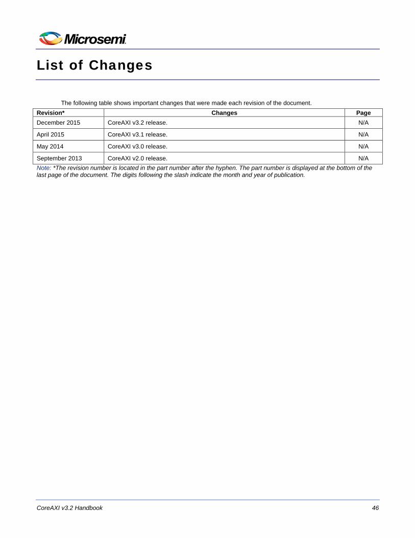
List of Changes
The following table shows important changes that were made each revision of the document. Revision* Changes Page December 2015 CoreAXI v3.2 release. N/A
April 2015 CoreAXI v3.1 release. N/A
May 2014 CoreAXI v3.0 release. N/A
September 2013 CoreAXI v2.0 release. N/A Note: *The revision number is located in the part number after the hyphen. The part number is displayed at the bottom of the last page of the document. The digits following the slash indicate the month and year of publication.

CoreAXI v3.2 Handbook 47
Product Support
Microsemi SoC Products Group backs its products with various support services, including Customer Service, Customer Technical Support Center, a website, electronic mail, and worldwide sales offices. This appendix contains information about contacting Microsemi SoC Products Group and using these support services.
Customer Service Contact Customer Service for non-technical product support, such as product pricing, product upgrades, update information, order status, and authorization.
From North America, call 800.262.1060 From the rest of the world, call 650.318.4460 Fax, from anywhere in the world 650. 318.8044
Customer Technical Support Center Microsemi SoC Products Group staffs its Customer Technical Support Center with highly skilled engineers who can help answer your hardware, software, and design questions about Microsemi SoC Products. The Customer Technical Support Center spends a great deal of time creating application notes, answers to common design cycle questions, documentation of known issues and various FAQs. So, before you contact us, please visit our online resources. It is very likely we have already answered your questions.
Technical Support For Microsemi SoC Products Support, visit http://www.microsemi.com/products/fpga-soc/design-support/fpga-soc-support.
Website You can browse a variety of technical and non-technical information on the Microsemi SoC Products Group home page, at http://www.microsemi.com/soc/.
Contacting the Customer Technical Support Center Highly skilled engineers staff the Technical Support Center. The Technical Support Center can be contacted by email or through the Microsemi SoC Products Group website.
Email You can communicate your technical questions to our email address and receive answers back by email, fax, or phone. Also, if you have design problems, you can email your design files to receive assistance. We constantly monitor the email account throughout the day. When sending your request to us, please be sure to include your full name, company name, and your contact information for efficient processing of your request. The technical support email address is [email protected].
My Cases Microsemi SoC Products Group customers may submit and track technical cases online by going to My Cases.

CoreAXI v3.2 Handbook
48 CoreAXI v3.2 Handbook
Outside the U.S. Customers needing assistance outside the US time zones can either contact technical support via email ([email protected]) or contact a local sales office. Sales office listings can be found at www.microsemi.com/soc/company/contact/default.aspx.
ITAR Technical Support For technical support on RH and RT FPGAs that are regulated by International Traffic in Arms Regulations (ITAR), contact us via [email protected]. Alternatively, within My Cases, select Yes in the ITAR drop-down list. For a complete list of ITAR-regulated Microsemi FPGAs, visit the ITAR web page.

50200393-4/12.15
Microsemi Corporation (Nasdaq: MSCC) offers a comprehensive portfolio of semiconductor and system solutions for communications, defense & security, aerospace and industrial markets. Products include high-performance and radiation-hardened analog mixed-signal integrated circuits, FPGAs, SoCs and ASICs; power management products; timing and synchronization devices and precise time solutions, setting the world’s standard for time; voice processing devices; RF solutions; discrete components; security technologies and scalable anti-tamper products; Ethernet solutions; Power-over-Ethernet ICs and midspans; as well as custom design capabilities and services. Microsemi is headquartered in Aliso Viejo, Calif., and has approximately 3,600 employees globally. Learn more at www.microsemi.com.
© 2015 Microsemi Corporation. All rights reserved. Microsemi and the Microsemi logo are trademarks of Microsemi Corporation. All other trademarks and service marks are the property of their respective owners.
Microsemi Corporate Headquarters One Enterprise, Aliso Viejo, CA 92656 USA Within the USA: +1 (800) 713-4113 Outside the USA: +1 (949) 380-6100 Sales: +1 (949) 380-6136 Fax: +1 (949) 215-4996 E-mail: [email protected]
Microsemi makes no warranty, representation, or guarantee regarding the information contained herein or the suitability of its products and services for any particular purpose, nor does Microsemi assume any liability whatsoever arising out of the application or use of any product or circuit. The products sold hereunder and any other products sold by Microsemi have been subject to limited testing and should not be used in conjunction with mission-critical equipment or applications. Any performance specifications are believed to be reliable but are not verified, and Buyer must conduct and complete all performance and other testing of the products, alone and together with, or installed in, any end-products. Buyer shall not rely on any data and performance specifications or parameters provided by Microsemi. It is the Buyer’s responsibility to independently determine suitability of any products and to test and verify the same. The information provided by Microsemi hereunder is provided “as is, where is” and with all faults, and the entire risk associated with such information is entirely with the Buyer. Microsemi does not grant, explicitly or implicitly, to any party any patent rights, licenses, or any other IP rights, whether with regard to such information itself or anything described by such information. Information provided in this document is proprietary to Microsemi, and Microsemi reserves the right to make any changes to the information in this document or to any products and services at any time without notice.