cont(mux) pd(mux) 11.4 : clock enabled edge-triggered flip-flop
Post on 21-Dec-2015
252 views
TRANSCRIPT
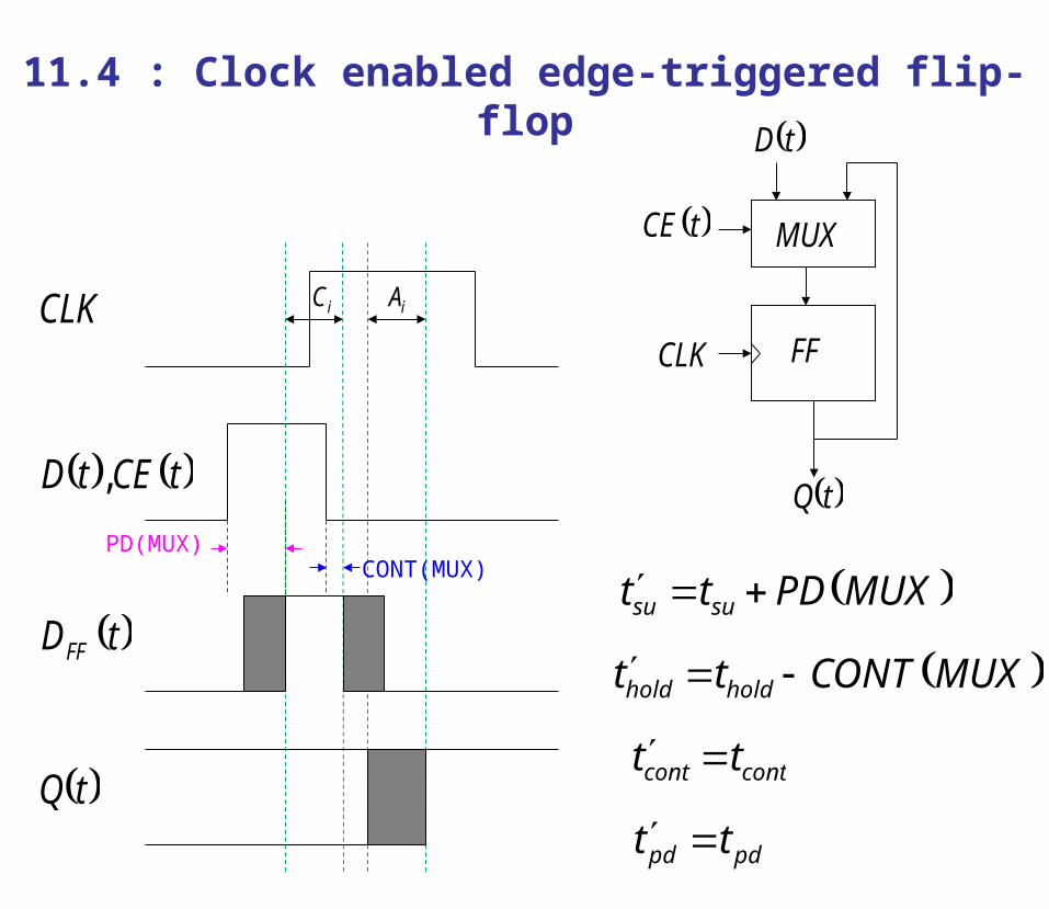
MUXPDtt susu
MUXCONTtt holdhold
contcont tt
pdpd tt
iC iACLK
tCEtD ,
tQ
tDFF
CONT(MUX)PD(MUX)
11.4 : Clock enabled edge-triggered flip-flop
MUX
FF
tD
tCE
CLK
tQ
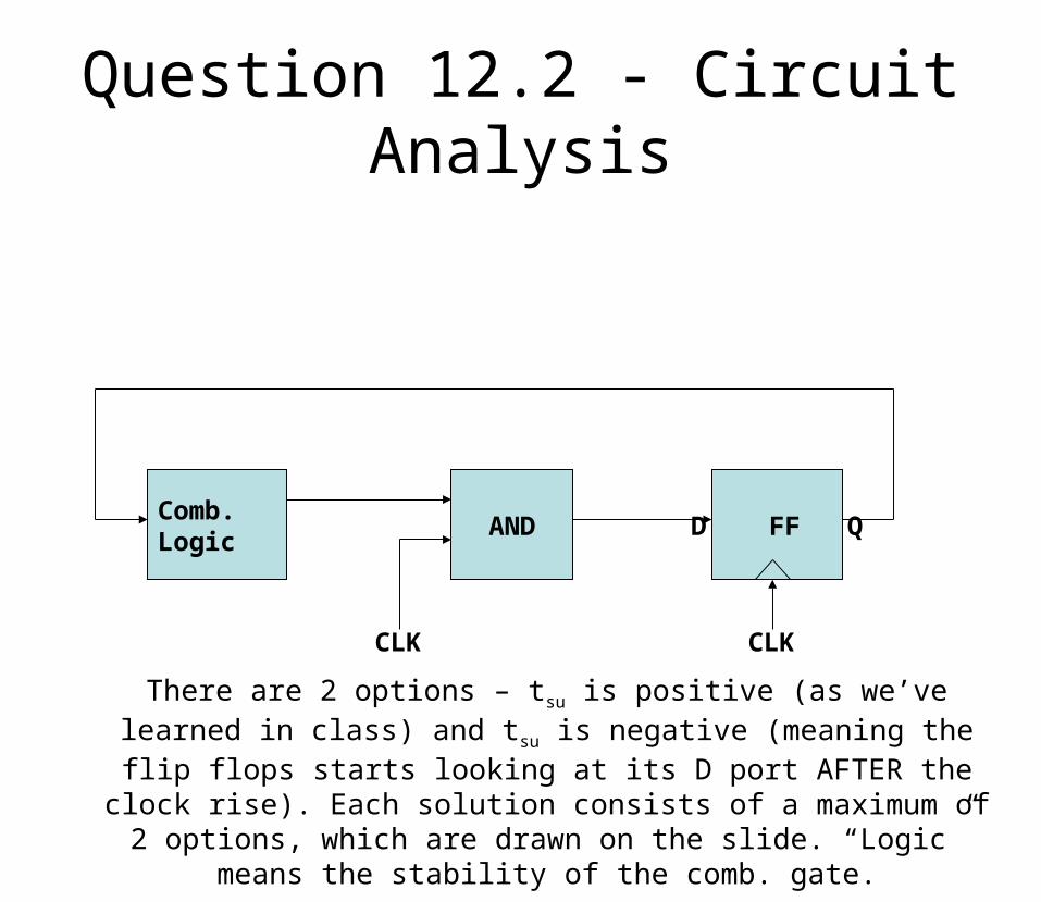
Question 12.2 - Circuit Analysis
Comb.Logic
AND D FF Q
CLKCLK
There are 2 options – tsu is positive (as we’ve learned in class) and tsu is negative (meaning the flip flops starts looking at its D port AFTER the clock rise). Each solution consists of a maximum of 2 options, which are drawn on the slide. “Logic” means the stability of the comb. gate.
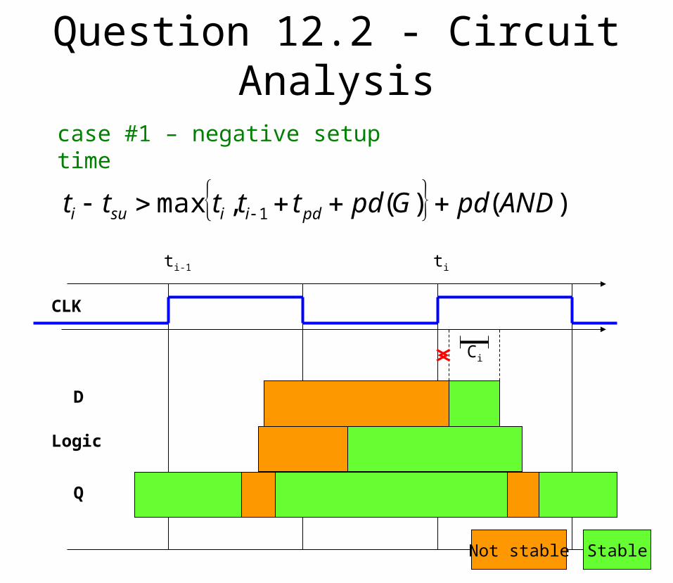
Question 12.2 - Circuit Analysis
CLK
case #1 – negative setup time
ti-1 ti
Ci
)()(,max 1 ANDpdGpdttttt pdiisui
Logic
Q
D
Not stable Stable
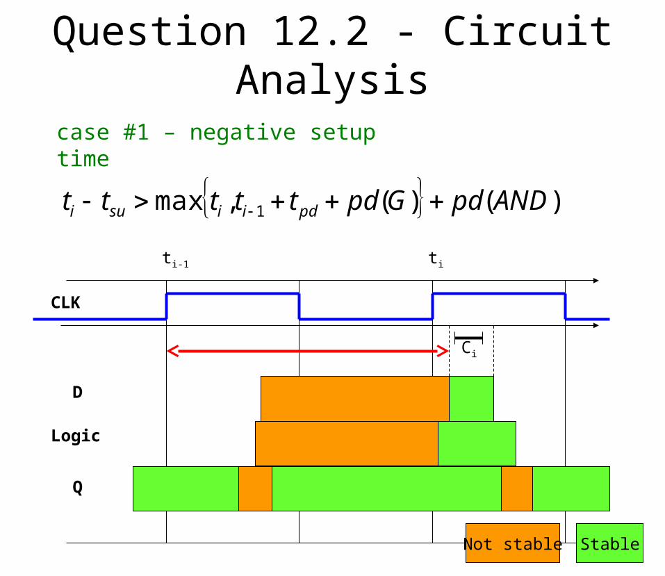
Question 12.2 - Circuit Analysis
CLK
case #1 – negative setup time
ti-1 ti
Ci
)()(,max 1 ANDpdGpdttttt pdiisui
Logic
Q
D
Not stable Stable
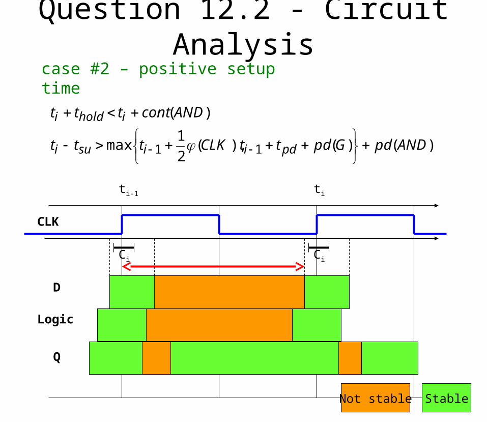
Question 12.2 - Circuit Analysis
CLK
case #2 – positive setup time
ti-1 ti
Ci
Logic
Q
D
Not stable Stable
)()(),(2
1max
)(
11 ANDpdGpdttCLKttt
ANDcontttt
pdiisui
iholdi
Ci
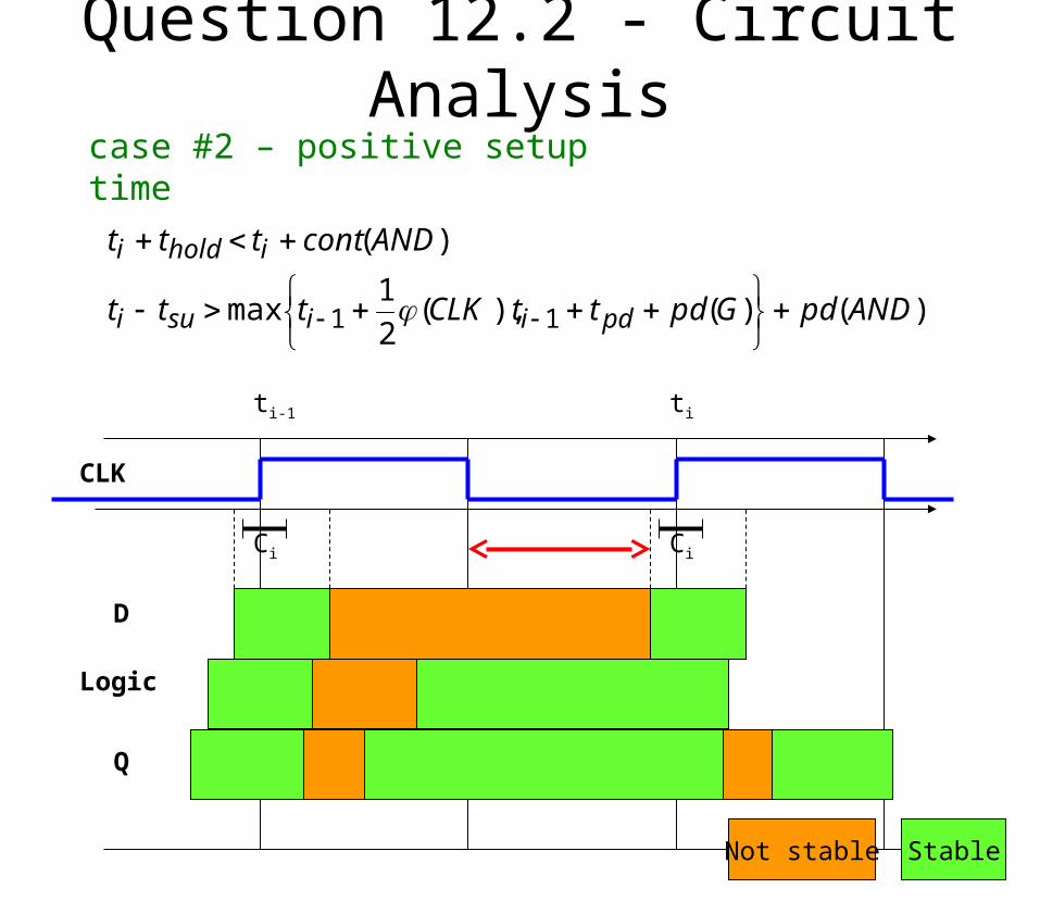
Question 12.2 - Circuit Analysis
CLK
case #2 – positive setup time
ti-1 ti
Ci
Logic
Q
D
Not stable Stable
)()(),(2
1max
)(
11 ANDpdGpdttCLKttt
ANDcontttt
pdiisui
iholdi
Ci

The Marvelous Toy
Toy Design
• Identifying system states
• Identifying state transitions and deciding on Moore or Mealy model
• Detailing the state machine transition and output functions
• The combinational circuits
• The Canonic circuit
• Clock rate calculation
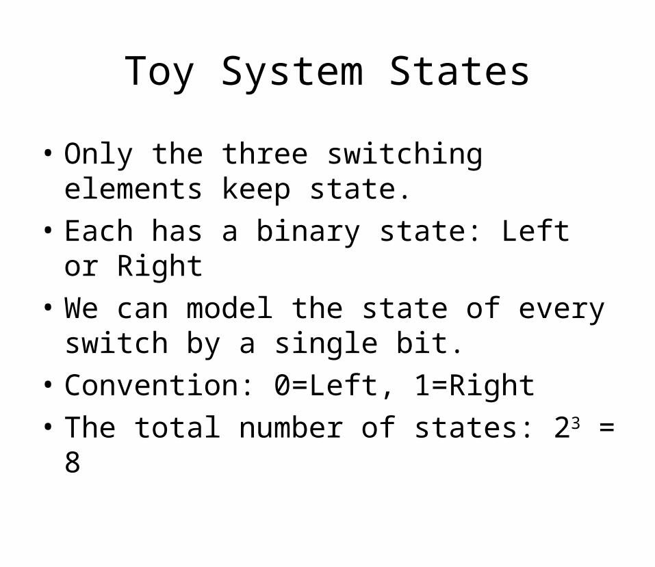
Toy System States
• Only the three switching elements keep state.
• Each has a binary state: Left or Right
• We can model the state of every switch by a single bit.
• Convention: 0=Left, 1=Right
• The total number of states: 23 = 8
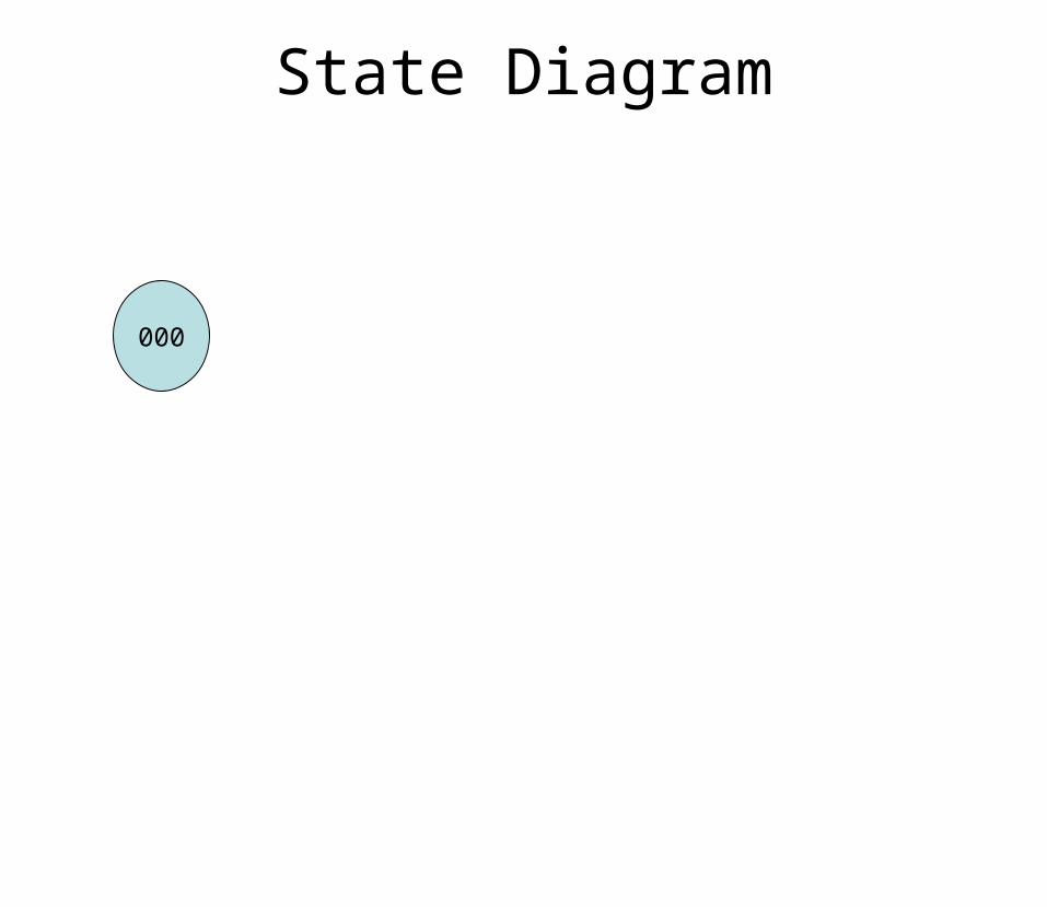
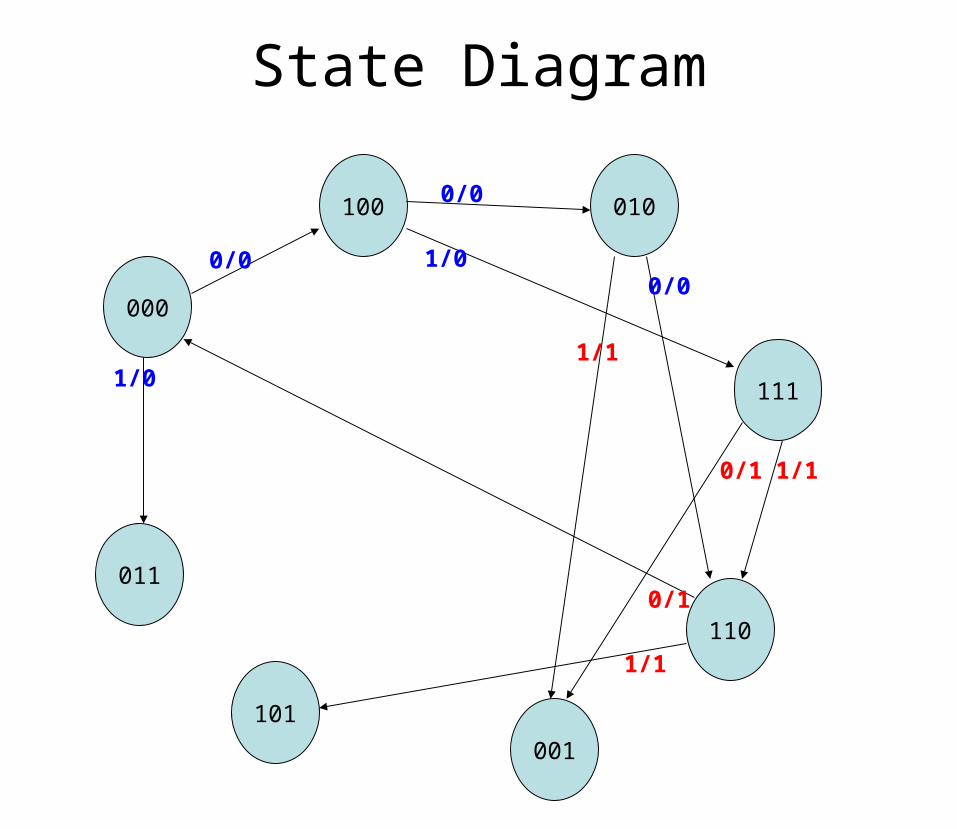
State Diagram
000
State Diagram
000
011
100
0/0
1/0
X is LeftZ is LeftY is Left
Enter from LeftOut from LeftSwap X
Enter from RightOut from LeftSwap Y & Z

State Diagram
000
011
100
0/0
1/0 111
0100/0
1/0
State Diagram
000
011
100
0/0
1/0 111
0100/0
1/0
110
001
0/0
1/1
Enter RightOut RightSwap Y&Z
State Diagram
000
011
100
0/0
1/0 111
0100/0
1/0
110
001
0/0
1/1
0/1 1/1
State Diagram
000
011
100
0/0
1/0 111
0100/0
1/0
101
110
001
0/0
1/1
0/1 1/1
0/1
1/1
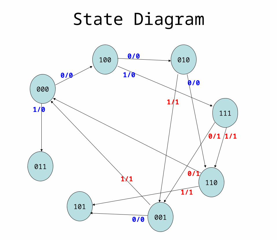
State Diagram
000
011
100
0/0
1/0 111
0100/0
1/0
101
110
001
0/0
1/1
0/1 1/1
0/1
1/1
0/0
1/1
State Diagram
000
011
100
0/0
1/0 111
0100/0
1/0
101
110
001
0/0
1/1
0/1 1/1
0/1
1/1
0/0
1/10/0
1/1

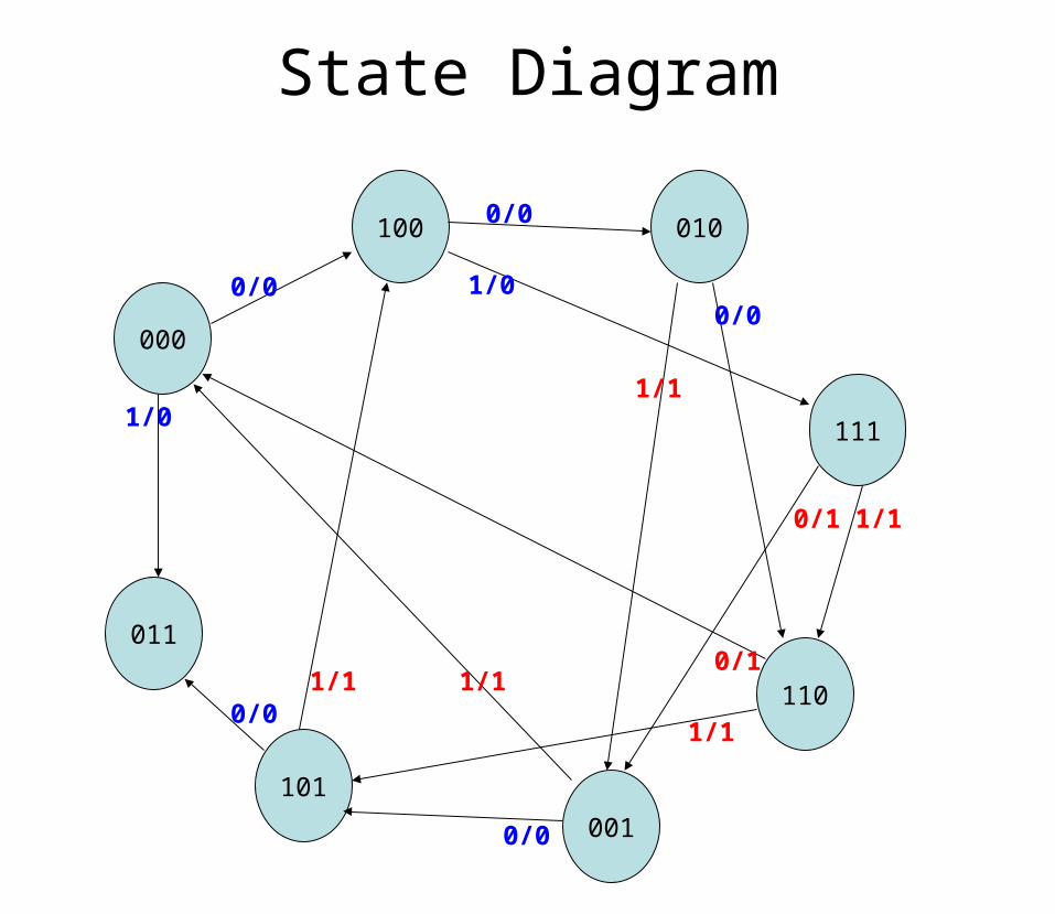
State Diagram
000
011
100
0/0
1/0 111
0100/0
1/0
101
110
001
0/0
1/1
0/1 1/1
0/1
1/1
0/0
1/1
0/0
1/1
0/01/1
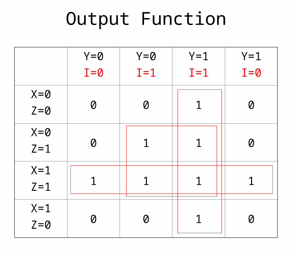
Output Function
Y=0I=0
Y=0I=1
Y=1I=1
Y=1I=0
X=0Z=0 0 0 1 0
X=0Z=1 0 1 1 0
X=1Z=1 1 1 1 1
X=1Z=0 0 0 1 0
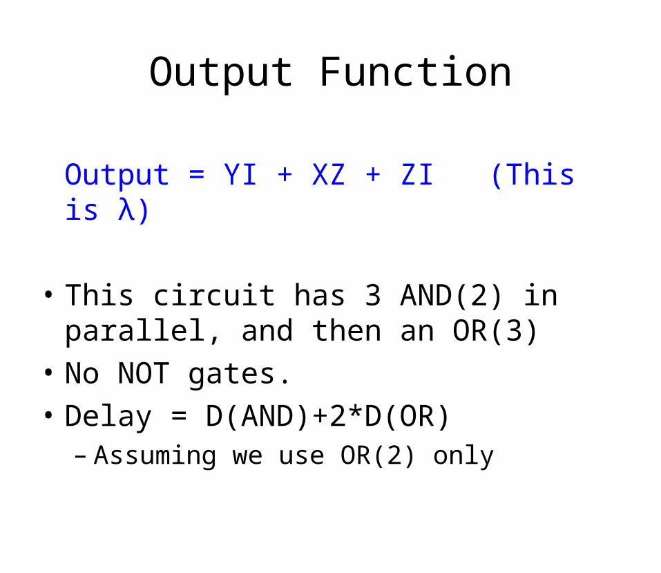
Output Function
Output = YI + XZ + ZI (This is λ)
• This circuit has 3 AND(2) in parallel, and then an OR(3)
• No NOT gates.
• Delay = D(AND)+2*D(OR)– Assuming we use OR(2) only

The Next State Function of X
000
011
100
0/0
1/0 111
0100/0
1/0
101
110
001
0/0
1/1
0/1 1/1
0/1
1/1
0/0
1/1
0/0
1/1
0/01/1

Next State Function for X
Y=0I=0
Y=0I=1
Y=1I=1
Y=1I=0
X=0Z=0 1 0 0 1
X=0Z=1 1 0 0 1
X=1Z=1 0 1 1 0
X=1Z=0 0 1 1 0

X Next State Function
X = X’I’+XI (This is part of δ)
• This circuit has: – 2 negations in parallel – 2 AND(2) in parallel, – and then an OR(2)
• Delay = D(NOT)+D(AND)+D(OR)
• Similar to this we find functions to Y,Z
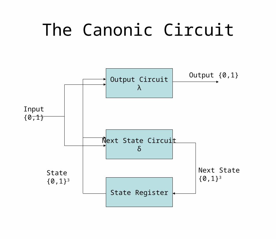
The Canonic Circuit
State Register
Next State Circuitδ
Output Circuitλ
Input {0,1}
Next State {0,1}3State {0,1}3
Output {0,1}

Stripping away the Flip-Flops
Next State Circuitδ
Output Circuitλ
Input {0,1}
Next State {0,1}3State {0,1}3
Output {0,1}
D-portQ-port
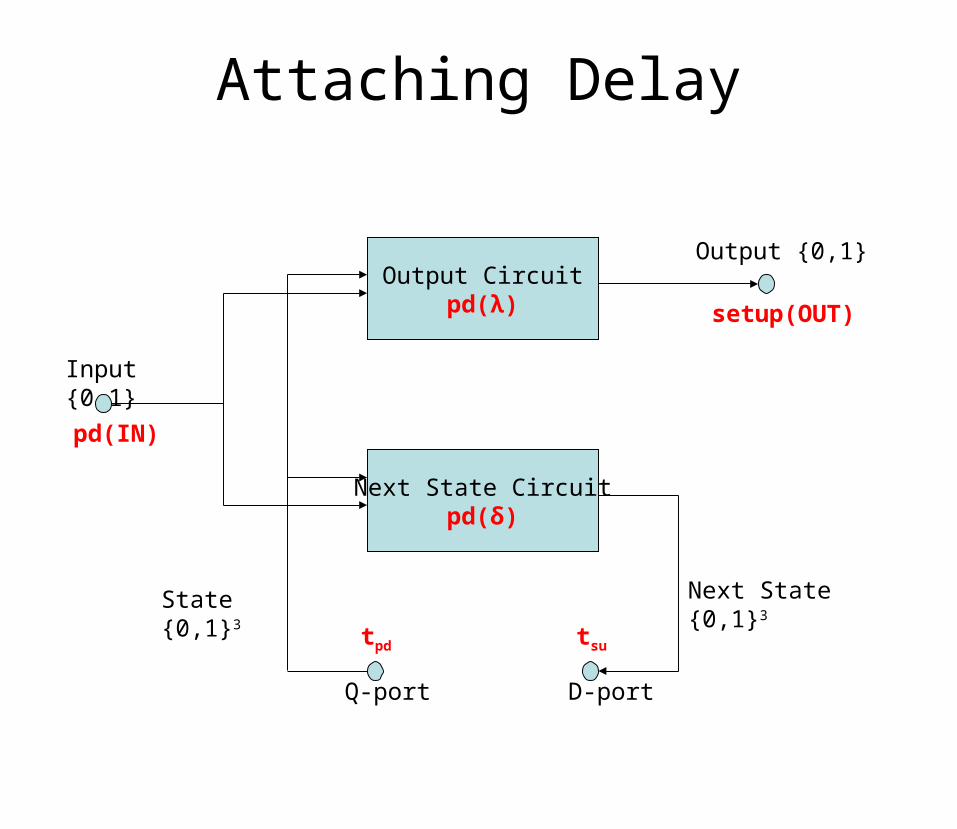
Attaching Delay
Next State Circuitpd(δ)
Output Circuitpd(λ)
Input {0,1}
Next State {0,1}3State {0,1}3
Output {0,1}
D-portQ-port
tpd
pd(IN)
setup(OUT)
tsu
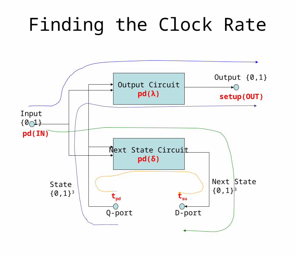
Finding the Clock Rate
Next State Circuitpd(δ)
Output Circuitpd(λ)
Input {0,1}
Next State {0,1}3State {0,1}3
Output {0,1}
D-portQ-port
tpd
pd(IN)
setup(OUT)
tsu
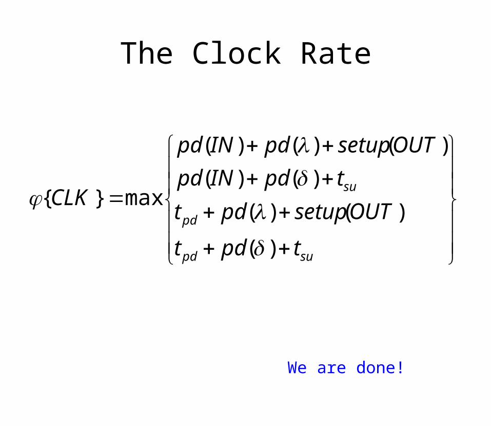
The Clock Rate
supd
pd
su
tpdt
OUTsetuppdt
tpdINpd
OUTsetuppdINpd
CLK
)(
)()(
)()(
)()()(
max}{
We are done!
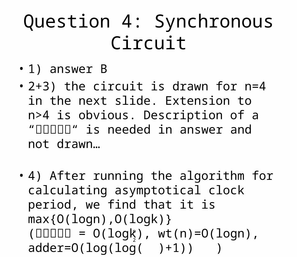
Question 4: Synchronous Circuit
• 1) answer B
• 2+3) the circuit is drawn for n=4 in the next slide. Extension to n>4 is obvious. Description of a “משוון“ is needed in answer and not drawn…
• 4) After running the algorithm for calculating asymptotical clock period, we find that it is max{O(logn),O(logk)} ,O(logk), wt(n)=O(logn) = משוון)adder=O(log(log( )+1)) )n
2
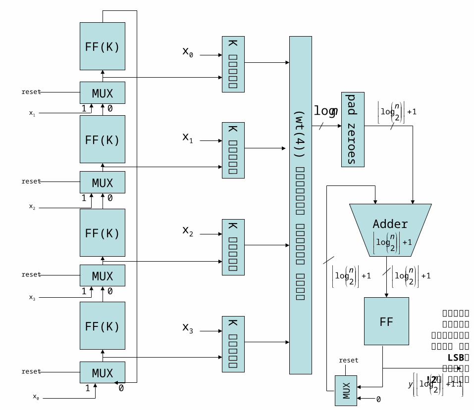
MUX
FF(K)
MUX
FF(K)
MUX
FF(K)
MUX
FF(K)
01x0
reset
0
0
0
reset
reset
reset
1x3
1x2
1x1
שוון מ
Kשוון
מK
שוון מ
Kשוון
מKx3
x2
x1
x0
ת (ארי
בינת
חרוזמ
קל ש
מw
t(4)(
pad zeroes
Adder
12
log
n
12
log
nnlog
FF
MU
X
0
reset
12
log
n1
2log
n
1:1
2log
ny
במוצא אנחנו
מורידים את LSBהביט הבשביל !2לחלק ב