connectivity to the asco power manager xp & 7000 … to the asco ... communications protocol as...
TRANSCRIPT
ASCO Power Technologies, L.P., 50 Hanover Rd., Florham Park, NJ 07932 USA www.asco.comModbus is a registered trademark of Gould Inc. 1 381339-221 I
Connectivity to the ASCO Power Manager Xp& 7000 Series Group 5 Controller via Modbus
This design specification describes the Modbuscommunications protocol as supported by the ASCOPower Manager Xp and 7000 Series Group 5Controller. It includes instructions on how to passinformation into and out of the either device via theModbus network. This publication should be used byindividuals wishing to integrate either device into theirfacility by developing software to communicate witheither device. Additional information can be found inPower Manager Xp Operator’s Manual 381333-199and Group 5 Controller User’s Guide 381333-126.
Modbus Protocol
Implementation BasicsThe following rules define the Modbus slaveimplementation of the devices:
The devices operate as slaves only(communication must be initiated by the master).
The maximum number of bytes contained withinone packet of communications is 64.
Transmission FormatAlthough the Modbus protocol supports both ASCIIand RTU modes of transmission, only the RTU modeis implemented. Within the RTU mode, the ASCOdevices support the following communicationparameters:
8 data bitsno parity1 stop bit
Modbus RTU Packet FormatEvery Modbus Packet consists of the following fields:
Device Address FieldFunction Code FieldData FieldError Check Field
Device Address Field. This is the first byte ofeach Modbus RTU transmission. The deviceaddress is a number limited to the range of 0 - 247and is associated with a single device configuredwith a matching address. Only the slave devicewhose address matches the value in this field willrespond to the specified command. Device address
0 indicates a broadcast command. This means thatevery slave on the network will act on thecommand, but it will not issue any responses.
Function Code Field. This is a second byte ofeach transmission and represents the commandedaction to the slave device (for queries from themaster) or the action that was taken by the slavedevice (for responses from the slave). Codesbetween 1 and 127 are defined as Modbus RTUfunctions. The function codes supported by thePower Manager Xp are detailed on page 4. Thefunction codes supported by the Group 5Controller are detailed on page 10.
Data Field. The data field varies in lengthdepending on whether the message is a request ora response packet. This field typically containsinformation required by the slave device toperform the command specified in a requestpacket or data being passed back by the slavedevice in a response packet.
Error Check Field. The error check fieldconsists of a 16 bit (2 byte) Cyclical RedundancyCheck (CRC16). It allows the receiving device todetect a packet that has been corrupted withtransmission errors. Refer to CRC-16 Algorithmon page 2 for details.
Packet Framing and TimingBecause the Modbus RTU protocol does not defineany explicit packet synchronization bytes, synchroniz-ation is accomplished implicitly with the use of silentintervals. According to the Modbus RTU standard, allmessages must start with a silent interval of at least 3.5character times. This means that every byte within apacket must precede the previous byte by fewer than3.5 character times based on the baud rate. And everynew packet of data must begin at least 3.5 charactertimes or more after the packet that had preceded it.
In summary, the three timing intervals associated withthe ASCO devices are as follows:
Maximum time between two consecutive byteswithin a packet < 3.5 character times.
Minimum time between two consecutivepackets is > 3.5 character times.
Maximum response time from a Master requestto a slave response is < 50 milliseconds.
ASCO Power Technologies, L.P., 50 Hanover Rd., Florham Park, NJ 07932 USA www.asco.com 381339-221 I2
CRC-16 AlgorithmProcedure. The algorithm essentially treats theentire data packet (less the start, stop, and, if used,parity bits) as one continuous binary number. Since weare doing a 16-bit CRC calculation, the binary number(entire packet) is multiplied by 216 and then divided bythe generator polynomial. In the case of the Modbusprotocol, the generator polynomial is x16 + x15 + x2 + 1.The 16-bit remainder of the division, which is the 16-bit CRC checksum, is then appended to the end of thepacket. The resulting data packet including the 16-bitCRC checksum, when divided by the same GeneratorPolynomial at the receiver, will give a zero remainderif no transmission errors have occurred.
The binary value of the Generator Polynomial is A001hex. This is obtained by first dropping the most-significant-bit of the polynomial and then reversing thebit order. This yields 1010000000000001 or A001h.
The steps for generating the 16-bit CRC checksum areas follows:
1. Initially, load the 16-bit CRC register with the valueFFFF hex.
2. Exclusive OR the 16-bit CRC register with the firstdata byte of the packet and store the result in the 16-bit CRC register.
3. If the Least Significant Bit (LSB) of the 16-bit CRCregister is equal to one, then shift the 16-bit CRCregister to the right by one bit and then ExclusiveOR the result with the generator polynomial, A001hex. Otherwise, just shift the 16-bit CRC register tothe right by one bit.
4. Repeat step 3 until eight right shifts have beenperformed.
5. Exclusive OR the 16-bit CRC register with the nextdata byte of the packet.
6. Repeat steps 3-5 until all the bytes of the data packethave been used in step 5.
7. The 16-bit CRC register contains the new checksumto be appended to the end of the packet, LeastSignificant Byte first.
CRC-16 Pseudocode. Below is the pseudocode for generating the 16-bit CRC checksum. XOR is theExclusive-OR function:
CRC16REG = FFFF hexGENPOLY = A001 hex
FOR X = 1 to number of bytes in packet BEGIN
XOR CRC16REG with the Xth data byteFOR Y = 1 to 8 BEGIN
IF [(the least-significant-bit of CRC16REG) = 1] THEN SHIFT CRC16REG one bit to the RIGHT XOR CRC16REG with GENPOLYOTHERWISE
SHIFT CRC16REG one bit to the RIGHT ENDNEXT Y
ENDNEXT X
The resulting CRC16REG contains the 16-bit CRC checksum
CRC-16 C Programming Language Example. CRC16_checksum is a C language function that calculatesand returns the 16-bit CRC checksum of a string of characters. This is the brute force method as it consumes a lotof processing power performing numerous bit shifts. A table look-up method based on this function would bemore suitable for embedded systems where processing power is at a premium. The following four parameters arepassed as part of the function
1. pointer to string2. length of string (in bytes)3. initial CRC value4. desired Generator polynomial
Included to make this CRC-16 function generic for any generator polynomialcontinued on next page
ASCO Power Technologies, L.P., 50 Hanover Rd., Florham Park, NJ 07932 USA www.asco.com 381339-221 I 3
The following C-language type definitions (typedef’s) are assumed:
1. typedef unsigned int uint;2. typedef unsigned char uchar;
The function is defined as follows:uint CRC16_checksum(uchar *Buffer, uint Length, uint CRC, uint Genpoly) {
uint index;
While (Length--) { /* for each data byte in string */
CRC = CRC ^ (uint) *Buffer++; /* exclusive OR data byte */
For (index = 0; index < 8; index++) { /* for each of the 8 bits */ If ((CRC & 0x0001) == 1) CRC = (CRC >> 1) ^ Genpoly; Else (CRC = CRC >> 1);
} /* for statement */
} /* while statement */
return(CRC);}
An ASCO Example. Let’s assume the transmitting device desired to send the ASCII string “ASCO”. Using anASCII character look-up table, we have the following hexadecimal codes for each of the ASCO letters:
A = 0x65S = 0x83C = 0x67O = 0x79
The transmitter would determine the 16-bit CRC checksum as follows (in C, both methods are equivalent):CRC16_checksum(“ASCO”, 4, 0xFFFF, 0xA001) which returns CRC = 0xCD94CRC16_checksum(“\x65\x83\x67\x79”, 4, 0xFFFF, 0xA001) which returns CRC = 0xCD94
Before sending the string, the transmitter would append the CRC checksum (in byte reverse order) to the string asfollows:
“ASCO\x94\xCD” or the equivalent in hexadecimal notation “\x65\x83\x67\x79\x94\xCD”
If the receiving device received the string without any transmission errors, then doing the 16-bit CRC checksumon the entire received string would yield (again, both methods are equivalent):
CRC16_checksum(“ASCO\x94\xCD”, 4, 0xFFFF, 0xA001) which returns CRC = 0x0000CRC16_checksum(“\x65\x83\x67\x79\x94\xCD”, 4, 0xFFFF, 0xA001) which returns CRC = 0x0000
Since the CRC checksum is equal to zero, the transmission is deemed valid.
Had an error been induced during the transmission, such as the ASCII character ‘A’ being inadvertently changedto the character ‘B’ (which is hexadecimal 0x66), the receiving device would determine the new checksum as:
CRC16_checksum(“BSCO\x94\xCD”, 4, 0xFFFF, 0xA001) which returns CRC = 0x3300CRC16_checksum(“\x66\x83\x67\x79\x94\xCD”, 4, 0xFFFF, 0xA001) which returns CRC = 0x3300
Since the CRC is NON-ZERO (0x3300), the receiver would assume an error had occurred and discard the packet.

ASCO Power Technologies, L.P., 50 Hanover Rd., Florham Park, NJ 07932 USA www.asco.com 381339-221 I4
Supported Function Codes for Power Manager Xp
Function # 03 (03h) – Read Holding RegistersThis function code allows the master to read one ormore consecutive data registers from the PowerManager Xp. The data registers are always 16 bit (twobyte) values, transmitted high order byte first. Refer toRegister Map on page 12 for details about the dataregister definitions of the Power Manager Xp.
The following example shows the format of atransmission between a master requesting device andthe responding Power Manager Xp (slave device) ataddress 24. The master desires to read the four valuesof current, IA, IB, IC, IAVE, beginning at Holdingregister location 40021 (which is a “Data startingaddress” of 20 decimal or 14 hexadecimal).
Master TransmissionPacket Format Example (in hex)
Slave address 18Function code 03Data starting address (high byte) 00Data starting address (low byte) 14Number of registers (high byte) 00Number of registers (low byte) 04CRC16 (low byte) 06CRC16 (high byte) 04
Slave ResponsePacket Format Example (in hex)
Slave address 18Function code 03Byte count 08Data word #1 (high byte) 04Data word #1 (low byte) CEData word #2 (high byte) 04Data word #2 (low byte) D3Data word #3 (high byte) 04Data word #3 (low byte) D3Data word #4 (high byte) 04Data word #4 (low byte) CECRC16 (low byte) 36CRC16 (high byte) 7F
The Power Manger Xp supports the following ReadHolding Register addresses-decimal: 11-26, 31-48,51-64, 71-84, 87-94, 96-125, 127-128, 130-137, 149-159. The Type of those Registers is defined as RO(Read only).
Function # 06 (06h) – Preset Single RegisterThis function code allows the master device to modifythe contents of a single configuration register withinthe Power Manager Xp. The data registers are always16 bit (two byte) values, transmitted high order bytefirst. Refer to Register Map on page 12 for details
about the about the data register definitions of thePower Manager Xp.
The Power Manager Xp currently supports thefollowing Preset Single register addresses. If aFunction #06 command is issued without one of theseregister addresses, the Power Manager Xp willrespond with an invalid address range ExceptionResponse (see Exception Responses on page 5).
AddressAddress(in hex
notation)Description
40095 005E Relay outputs (DO1-DO4)40200 00C7 System type40201 00C8 Source mode40202 00C9 Potential transformer ratio (PTR)40203 00CA Current transformer ratio (CTR)40204 00CB Neutral current transformer ratio
(CT4R)40205 00CC SCI comm. port (J5) protocol40206 00CD SCI comm. port (J5) baud rate40207 00CE SCI comm. port (J5) device
address40208 00CC 485 comm. Port (J1) protocol40209 00CD 485 comm. Port (J1) baud rate40210 00CE 485 comm. port (J1) device
address40211 00CF Menu language selection40212 00D0 Demand window size (in minutes)40213 00D1 Demand subinterval size (fixed at
1 minute)40214 00D2 Reset inst. & max. demand
registers40215 00D3 Reset energy registers
The following example shows the format of atransmission between a master device and theresponding Power Manager Xp (slave device) ataddress 24. The master desires to set the System Type(Holding register 40200) to a Single Phase – 3 Wiresystem (data value 02). See System Type on page 7 fordetails.
Master TransmissionPacket Format Example (in hex)
Slave address 18Function code 06Data address (high byte) 00Data address (low byte) C7Data word (high byte) 00Data word (low byte) 02CRC16 (low byte) BBCRC16 (high byte) FF

ASCO Power Technologies, L.P., 50 Hanover Rd., Florham Park, NJ 07932 USA www.asco.com 381339-221 I 5
Slave ResponsePacket Format Example (in hex)
Slave address 18Function code 06Data starting address (high byte) 00Data starting address (low byte) C7Number of registers (high byte) 00Number of registers (low byte) 02CRC16 (low byte) BBCRC16 (high byte) FF
The Power Manger Xp supports the following PresetSingle Register addresses -decimal: 65-68, 95, 148,160, and 200-215.
Function # 16 (10h) – Preset Multiple RegistersThis function code allows the master device to modifythe contents of consecutive configuration registerswithin the Power Manager Xp. The data registers arealways 16 bit (two byte) values, transmitted high orderbyte first. Refer to Register Map on page 12 for detailsabout the data register definitions of the PowerManager Xp.
The Power Manager Xp currently supports thefollowing Preset Multiple register ranges. If a Function#16 command is issued without one of thesecorresponding register ranges, the Power Manager Xpwill respond with an invalid address range ExceptionResponse (see Exception Responses on page 6).
AddressStart End
RegisterCount
Description Command String (in Hex)
40141 40146 6 PM Date & Time ADDR 10 00 8C 00 06 0C ..data.. CRCLO CRCHI40200 40213 14 General Settings ADDR 10 00 C7 00 0E 1C ..data.. CRCLO CRCHI40230 40235 6 Setpoint Settings ADDR 10 00 E5 00 06 0C ..data.. CRCLO CRCHI40326 40333 8 S1 Status Input #1 name ADDR 10 01 45 00 08 10 ..data.. CRCLO CRCHI40334 40341 8 S2 Status Input #2 name ADDR 10 01 4D 00 08 10 ..data.. CRCLO CRCHI40342 40349 8 S3 Status Input #3 name ADDR 10 01 55 00 08 10 ..data.. CRCLO CRCHI40350 40357 8 S4 Status Input #4 name ADDR 10 01 5D 00 08 10 ..data.. CRCLO CRCHI40358 40365 8 S5 Status Input #5 name ADDR 10 01 65 00 08 10 ..data.. CRCLO CRCHI40366 40373 8 S6 Status Input #6 name ADDR 10 01 6D 00 08 10 ..data.. CRCLO CRCHI40374 40381 8 S7 Status Input #7 name ADDR 10 01 75 00 08 10 ..data.. CRCLO CRCHI40382 40389 8 S8 Status Input #8 name ADDR 10 01 7D 00 08 10 ..data.. CRCLO CRCHI40390 40397 8 Relay Output #1 name ADDR 10 01 85 00 08 10 ..data.. CRCLO CRCHI40398 40405 8 Relay Output #2 name ADDR 10 01 8D 00 08 10 ..data.. CRCLO CRCHI40406 40413 8 Relay Output #3 name ADDR 10 01 95 00 08 10 ..data.. CRCLO CRCHI40414 40421 8 Relay Output #4 name ADDR 10 01 9D 00 08 10 ..data.. CRCLO CRCHI
The following example shows the format of atransmission between a master requesting device andthe responding Power Manager Xp (slave device) ataddress 24. The master desires to configure Setpoint#1 (Holding Registers 40230 – 40235).
Slave ResponsePacket Format Example (in hex)
Slave address 18Function code 10Data starting address (high byte) 00Data starting address (low byte) E5Number of registers (high byte) 00Number of registers (low byte) 06CRC16 (low byte) 53CRC16 (high byte) F5
The Power Manger Xp supports the following PresetSingle Register addresses -decimal: 141-146, 200-213,230-235, 236-319, 322-325, 326-421, and 422-433.
Master TransmissionPacket Format Example (in hex)
Slave address 18Function code 10Data starting address (high byte) 00Data starting address (low byte) E5Number of registers (high byte) 00Number of registers (low byte) 06Byte count 0CData word #1 (high byte) 00Data word #1 (low byte) 01Data word #2 (high byte) 03Data word #2 (low byte) E8Data word #3 (high byte) 00Data word #3 (low byte) 00Data word #4 (high byte) 03Data word #4 (low byte) 20Data word #5 (high byte) 00Data word #5 (low byte) 05Data word #6 (high byte) 00Data word #6 (low byte) 02CRC16 (low byte) D1CRC16 (high byte) 91

ASCO Power Technologies, L.P., 50 Hanover Rd., Florham Park, NJ 07932 USA www.asco.com 381339-221 I6
Exception ResponsesIf the Modbus master device sends an unsupportedcommand, attempts to read an invalid holding register,or attempts to write invalid data, the Power ManagerXp (Modbus slave) issues an exception response. Theformat for the exception response is as follows:
1. SLAVE ADDRESS2. FUNCTION CODE*
(with the most-significant-bit set to a 1)3. ERROR CODE4. CRC16 – low order byte5. CRC16 – high order byte
* Note: The high order bit of the function codehas been set to one to indicate an exceptionresponse has been generated.
The following table is a list of the exception codessupported by the Power Manager Xp.
Exception Response Error CodesErrorcode
Errorname
Power Manager Xpimplementation
01Illegal
functionThe slave does not support thefunction code contained in the masterquery packet.
02Illegaldata
address
The slave does not support the HoldingRegister address referenced in thedata field of the master query packet.
03Illegaldatavalue
The slave does not support the datareferenced in the data field of themaster query packet.
04Devicefailure
The addresses slave is unable toperform the action requested due to aninternal failure or malfunction.
The following example shows the format of a trans-mission between a master device and the respondingPower Manager Xp (slave device) at address 24. Themaster device attempts to write an invalid data value(04) to the System Type holding register 40200. ThePower Manager Xp slave device responds with Errorcode 03.
Master TransmissionPacket Format Example (in hex)
Slave address 18Function code 06Data starting address (high byte) 00Data starting address (low byte) C7Data (high byte) 00Data (low byte) 04CRC16 (low byte) 3BCRC16 (high byte) FD
Slave ResponsePacket Format Example (in hex)
Slave address 18Function code 86Error code 03CRC16 (low byte) D3CRC16 (high byte) A6
The following example shows the format of atransmission between a master device and theresponding Power Manager Xp (slave device) ataddress 24. The master device attempts to write to aninvalid address, 40216 (0x00D7). The Power ManagerXp slave device responds with Error code 02.
Master TransmissionPacket Format Example (in hex)
Slave address 18Function code 06Data starting address (high byte) 00Data starting address (low byte) D7Data (high byte) 00Data (low byte) 03CRC16 (low byte) 7BCRC16 (high byte) FA
Slave ResponsePacket Format Example (in hex)
Slave address 18Function code 86Error code 02CRC16 (low byte) 12CRC16 (high byte) 66
ASCO Power Technologies, L.P., 50 Hanover Rd., Florham Park, NJ 07932 USA www.asco.com 381339-221 I 7
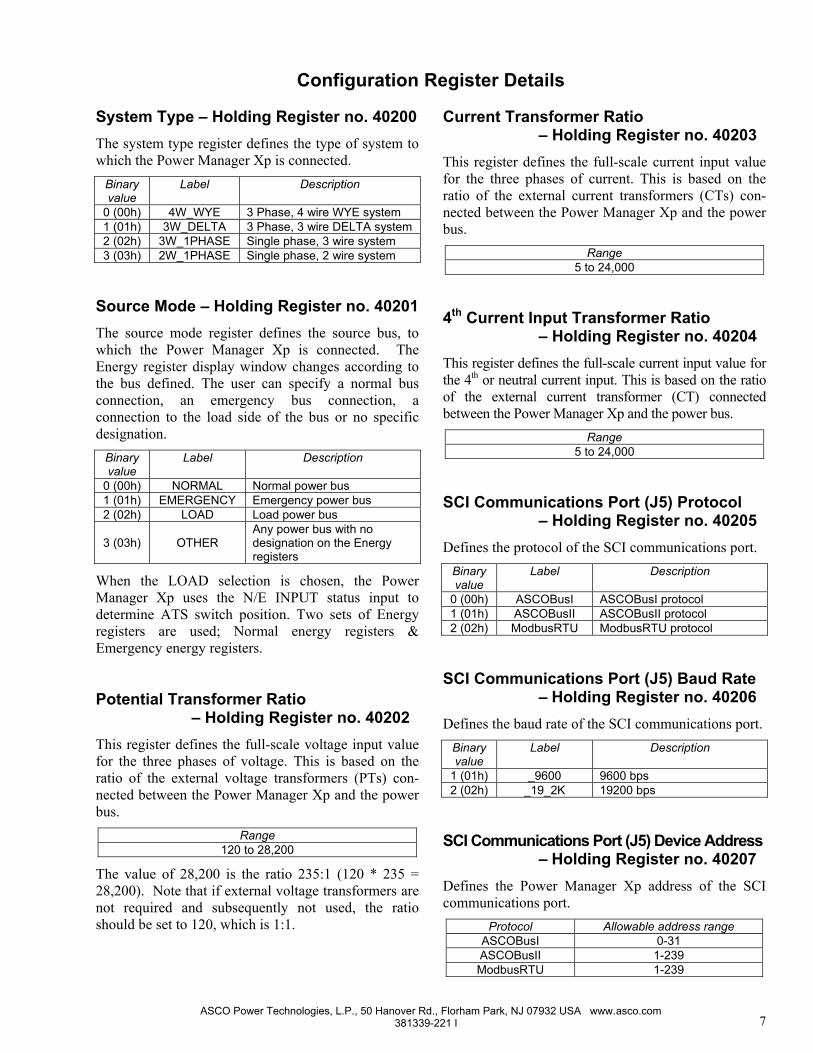
Configuration Register Details
System Type – Holding Register no. 40200The system type register defines the type of system towhich the Power Manager Xp is connected.
Binaryvalue
Label Description
0 (00h) 4W_WYE 3 Phase, 4 wire WYE system1 (01h) 3W_DELTA 3 Phase, 3 wire DELTA system2 (02h) 3W_1PHASE Single phase, 3 wire system3 (03h) 2W_1PHASE Single phase, 2 wire system
Source Mode – Holding Register no. 40201The source mode register defines the source bus, towhich the Power Manager Xp is connected. TheEnergy register display window changes according tothe bus defined. The user can specify a normal busconnection, an emergency bus connection, aconnection to the load side of the bus or no specificdesignation.
Binaryvalue
Label Description
0 (00h) NORMAL Normal power bus1 (01h) EMERGENCY Emergency power bus2 (02h) LOAD Load power bus
3 (03h) OTHERAny power bus with nodesignation on the Energyregisters
When the LOAD selection is chosen, the PowerManager Xp uses the N/E INPUT status input todetermine ATS switch position. Two sets of Energyregisters are used; Normal energy registers &Emergency energy registers.
Potential Transformer Ratio– Holding Register no. 40202
This register defines the full-scale voltage input valuefor the three phases of voltage. This is based on theratio of the external voltage transformers (PTs) con-nected between the Power Manager Xp and the powerbus.
Range120 to 28,200
The value of 28,200 is the ratio 235:1 (120 * 235 =28,200). Note that if external voltage transformers arenot required and subsequently not used, the ratioshould be set to 120, which is 1:1.
Current Transformer Ratio– Holding Register no. 40203
This register defines the full-scale current input valuefor the three phases of current. This is based on theratio of the external current transformers (CTs) con-nected between the Power Manager Xp and the powerbus.
Range5 to 24,000
4th Current Input Transformer Ratio– Holding Register no. 40204
This register defines the full-scale current input value forthe 4th or neutral current input. This is based on the ratioof the external current transformer (CT) connectedbetween the Power Manager Xp and the power bus.
Range5 to 24,000
SCI Communications Port (J5) Protocol– Holding Register no. 40205
Defines the protocol of the SCI communications port.Binaryvalue
Label Description
0 (00h) ASCOBusI ASCOBusI protocol1 (01h) ASCOBusII ASCOBusII protocol2 (02h) ModbusRTU ModbusRTU protocol
SCI Communications Port (J5) Baud Rate– Holding Register no. 40206
Defines the baud rate of the SCI communications port.Binaryvalue
Label Description
1 (01h) _9600 9600 bps2 (02h) _19_2K 19200 bps
SCI Communications Port (J5) Device Address– Holding Register no. 40207
Defines the Power Manager Xp address of the SCIcommunications port.
Protocol Allowable address rangeASCOBusI 0-31ASCOBusII 1-239ModbusRTU 1-239

ASCO Power Technologies, L.P., 50 Hanover Rd., Florham Park, NJ 07932 USA www.asco.com 381339-221 I8
485 Communications Port (J1) Protocol– Holding Register no. 40208
Defines the protocol of the dedicated RS-485communications port, if present on Power ManagerXp. ‡
Binaryvalue
Label Description
0 (00h) ASCOBusI ASCOBusI protocol1 (01h) ASCOBusII ASCOBusII protocol2 (02h) ModbusRTU ModbusRTU protocol
485 Communications Port (J1) Baud Rate– Holding Register no. 40209
Defines the baud rate of the dedicated RS-485communications port, if present on Power ManagerXp. ‡
Binaryvalue
Label Description
1 (01h) _9600 9600 bps2 (02h) _19_2K 19200 bps3 (03h) _38_4K 38400 bps4 (04h) _57_6K 57600 bps
485 Communications Port (J1) Device Address– Holding Register no. 40210
Defines the Power Manager Xp address of thededicated RS-485 communications port, if present onPower Manager Xp.‡
Protocol Allowable address rangeASCOBusI 0-31ASCOBusII 1-239ModbusRTU 1-239
‡ Power Managers with Transducers part # 629168 (Catalog 5200T) support the RS-485 com port J1. Data Monitors with Electronic Access Module part # 607607 Rev E or higher support the RS-485 com port J1.
Language – Holding Register no. 40211Defines the Language displayed on the liquid crystaldisplay (LCD) interface.
Binaryvalue
Label Description
0 (00h) ENGLISH English language** Currently only the English language is available.
Demand Window Size– Holding Register no. 40212
Defines the length of the demand period, in minutes,used in calculating the sliding window demand values.
Range1 to 15
Subinterval Size– Holding Register no. 40213
Defines the length of the subinterval demand period, inminutes, used in calculating the sliding windowdemand values. This value is fixed at 1 minute.
Range1
Reset Demand– Holding Register no. 40214
Writing a value of 0xFFFF to this holding registerclears the Minimum and Maximum KWDemandregisters.
Clear Energy– Holding Register no. 40215
Writing a value of 0xFFFF to this holding registerclears the Energy registers.
Part no.629168or607607Rev. E
ASCO Power Technologies, L.P., 50 Hanover Rd., Florham Park, NJ 07932 USA www.asco.com 381339-221 I 9
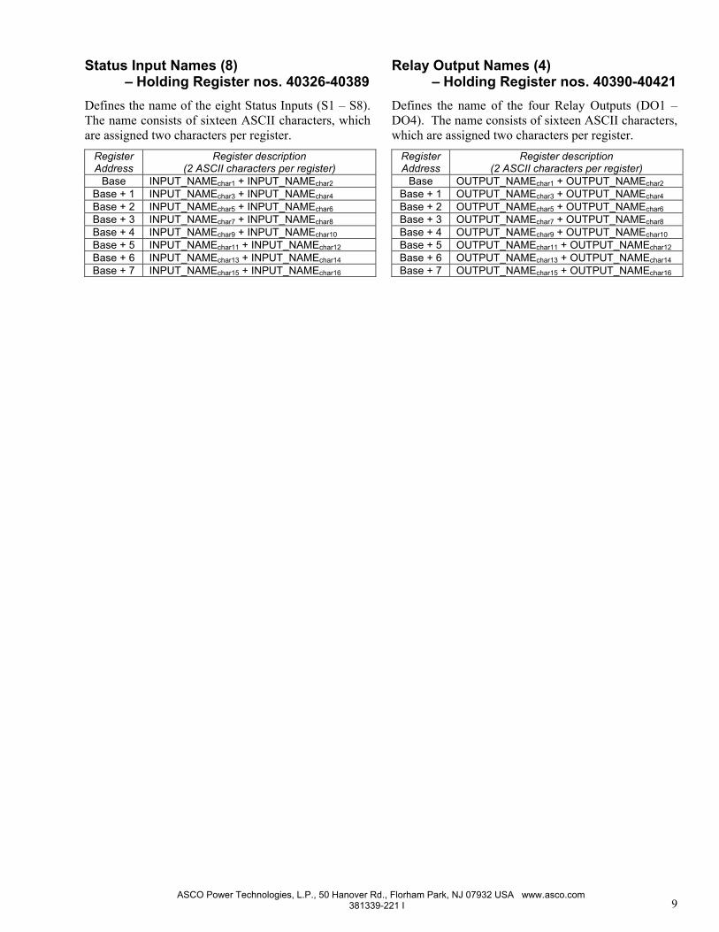
Status Input Names (8) – Holding Register nos. 40326-40389
Defines the name of the eight Status Inputs (S1 – S8).The name consists of sixteen ASCII characters, whichare assigned two characters per register.
RegisterAddress
Register description(2 ASCII characters per register)
Base INPUT_NAMEchar1 + INPUT_NAMEchar2Base + 1 INPUT_NAMEchar3 + INPUT_NAMEchar4Base + 2 INPUT_NAMEchar5 + INPUT_NAMEchar6Base + 3 INPUT_NAMEchar7 + INPUT_NAMEchar8Base + 4 INPUT_NAMEchar9 + INPUT_NAMEchar10Base + 5 INPUT_NAMEchar11 + INPUT_NAMEchar12Base + 6 INPUT_NAMEchar13 + INPUT_NAMEchar14Base + 7 INPUT_NAMEchar15 + INPUT_NAMEchar16
Relay Output Names (4) – Holding Register nos. 40390-40421
Defines the name of the four Relay Outputs (DO1 –DO4). The name consists of sixteen ASCII characters,which are assigned two characters per register.
RegisterAddress
Register description(2 ASCII characters per register)
Base OUTPUT_NAMEchar1 + OUTPUT_NAMEchar2Base + 1 OUTPUT_NAMEchar3 + OUTPUT_NAMEchar4Base + 2 OUTPUT_NAMEchar5 + OUTPUT_NAMEchar6Base + 3 OUTPUT_NAMEchar7 + OUTPUT_NAMEchar8Base + 4 OUTPUT_NAMEchar9 + OUTPUT_NAMEchar10Base + 5 OUTPUT_NAMEchar11 + OUTPUT_NAMEchar12Base + 6 OUTPUT_NAMEchar13 + OUTPUT_NAMEchar14Base + 7 OUTPUT_NAMEchar15 + OUTPUT_NAMEchar16
ASCO Power Technologies, L.P., 50 Hanover Rd., Florham Park, NJ 07932 USA www.asco.com 381339-221 I10
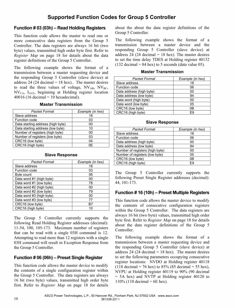
Supported Function Codes for Group 5 Controller
Function # 03 (03h) – Read Holding RegistersThis function code allows the master to read one ormore consecutive data registers from the Group 5Controller. The data registers are always 16 bit (twobyte) values, transmitted high order byte first. Refer toRegister Map on page 18 for details about the dataregister definitions of the Group 5 Controller.
The following example shows the format of atransmission between a master requesting device andthe responding Group 5 Controller (slave device) ataddress 24 (24 decimal = 18 hex).. The master desiresto read the three values of voltage, NVAB, NVBC,NVCA, IAVE, beginning at Holding register location40016 (16 decimal = 10 hexadecimal).
Master TransmissionPacket Format Example (in hex)
Slave address 18Function code 03Data starting address (high byte) 00Data starting address (low byte) 10Number of registers (high byte) 00Number of registers (low byte) 03CRC16 (low byte) 04CRC16 (high byte) 0E
Slave ResponsePacket Format Example (in hex)
Slave address 18Function code 03Byte count 06Data word #1 (high byte) 00Data word #1 (low byte) 78Data word #2 (high byte) 00Data word #2 (low byte) 79Data word #3 (high byte) 00Data word #3 (low byte) 77CRC16 (low byte) B7CRC16 (high byte) 10
The Group 5 Controller currently supports thefollowing Read Holding Register addresses (decimal):11-54, 100, 105-173. Maximum number of registersthat can be read with a single 03H command is 12.Attempting to read more than 12 registers with a single03H command will result in Exception Response fromthe Group 5 Controller.
Function # 06 (06h) – Preset Single RegisterThis function code allows the master device to modifythe contents of a single configuration register withinthe Group 5 Controller. The data registers are always16 bit (two byte) values, transmitted high order bytefirst. Refer to Register Map on page 18 for details
about the about the data register definitions of theGroup 5 Controller.
The following example shows the format of atransmission between a master device and theresponding Group 5 Controller (slave device) ataddress 24 (24 decimal = 18 hex). The master desiresto set the time delay TDES at Holding register 40132(132 decimal = 84 hex) to 5 seconds (data value 05).
Master TransmissionPacket Format Example (in hex)
Slave address 18Function code 06Data address (high byte) 00Data address (low byte) 84Data word (high byte) 00Data word (low byte) 05CRC16 (low byte) 0BCRC16 (high byte) E9
Slave ResponsePacket Format Example (in hex)
Slave address 18Function code 06Data address (high byte) 00Data address (low byte) 84Number of registers (high byte) 00Number of registers (low byte) 05CRC16 (low byte) 0BCRC16 (high byte) E9
The Group 5 Controller currently supports thefollowing Preset Single Register addresses (decimal):44, 101-173.
Function # 16 (10h) – Preset Multiple RegistersThis function code allows the master device to modifythe contents of consecutive configuration registerswithin the Group 5 Controller. The data registers arealways 16 bit (two byte) values, transmitted high orderbyte first. Refer to Register Map on page 18 for detailsabout the data register definitions of the Group 5Controller.
The following example shows the format of atransmission between a master requesting device andthe responding Group 5 Controller (slave device) ataddress 24 (24 decimal = 18 hex). The master desiresto set the following parameters occupying consecutiveregister locations: NVDO at Holding register 40118(118 decimal = 76 hex) to 85% (85 decimal = 55 hex),NVPU at Holding register 40119 to 90% (90 decimal= 5A hex) and NVTP at Holding register 40120 to110% (110 decimal = 6E hex).
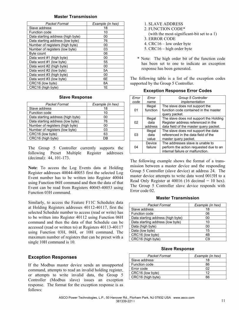
ASCO Power Technologies, L.P., 50 Hanover Rd., Florham Park, NJ 07932 USA www.asco.com 381339-221 I 11
Master TransmissionPacket Format Example (in hex)
Slave address 18Function code 10Data starting address (high byte) 00Data starting address (low byte) 76Number of registers (high byte) 00Number of registers (low byte) 03Byte count 06Data word #1 (high byte) 00Data word #1 (low byte) 55Data word #2 (high byte) 00Data word #2 (low byte) 5AData word #3 (high byte) 00Data word #3 (low byte) 6ECRC16 (low byte) 8ACRC16 (high byte) 1E
Slave ResponsePacket Format Example (in hex)
Slave address 18Function code 10Data starting address (high byte) 00Data starting address (low byte) 76Number of registers (high byte) 00Number of registers (low byte) 03CRC16 (low byte) 63CRC16 (high byte) DB
The Group 5 Controller currently supports thefollowing Preset Multiple Register addresses(decimal): 44, 101-173.
Note: To access the Log Events data at HoldingRegister addresses 40044-40053 first the selected LogEvent number has to be written into Register 40044using Function 06H command and then the data of thatEvent can be read from Registers 40045-40053 usingFunction 03H command.
Similarly, to access the Feature F11C Schedules dataat Holding Registers addresses 40112-40117, first theselected Schedule number to access (read or write) hasto be written into Register 40112 using Function 06Hcommand and then the data of that Schedule can beaccessed (read or written to) at Registers 40113-40117using Function 03H, 06H, or 10H command. Themaximum number of registers that can be preset with asingle 10H command is 10.
Exception ResponsesIf the Modbus master device sends an unsupportedcommand, attempts to read an invalid holding register,or attempts to write invalid data, the Group 5Controller (Modbus slave) issues an exceptionresponse. The format for the exception response is asfollows:
1. SLAVE ADDRESS2. FUNCTION CODE*
(with the most-significant-bit set to a 1)3. ERROR CODE4. CRC16 – low order byte5. CRC16 – high order byte
* Note: The high order bit of the function codehas been set to one to indicate an exceptionresponse has been generated.
The following table is a list of the exception codessupported by the Group 5 Controller.
Exception Response Error CodesErrorcode
Errorname
Group 5 Controllerimplementation
01Illegal
functionThe slave does not support thefunction code contained in the masterquery packet.
02Illegaldata
address
The slave does not support the HoldingRegister address referenced in thedata field of the master query packet.
03Illegaldatavalue
The slave does not support the datareferenced in the data field of themaster query packet.
04Devicefailure
The addresses slave is unable toperform the action requested due to aninternal failure or malfunction.
The following example shows the format of a trans-mission between a master device and the respondingGroup 5 Controller (slave device) at address 24. Themaster device attempts to write data word 0015H to aRead Only Register at 40016 (16 decimal = 10 hex).The Group 5 Controller slave device responds withError code 02.
Master TransmissionPacket Format Example (in hex)
Slave address 18Function code 06Data starting address (high byte) 00Data starting address (low byte) 10Data (high byte) 00Data (low byte) 15CRC16 (low byte) 4BCRC16 (high byte) C9
Slave ResponsePacket Format Example (in hex)
Slave address 18Function code 86Error code 02CRC16 (low byte) 12CRC16 (high byte) 66
ASCO Power Technologies, L.P., 50 Hanover Rd., Florham Park, NJ 07932 USA www.asco.comModbus is a registered trademark of Gould Inc. 1 381339-221 I
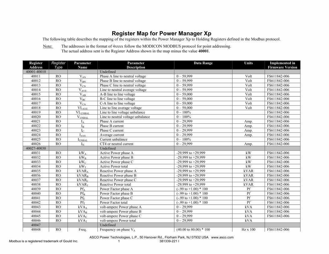
Register Map for Power Manager XpThe following table describes the mapping of the registers within the Power Manager Xp to Holding Registers defined in the Modbus protocol.
Note: The addresses in the format of 4xxxx follow the MODICON MODBUS protocol for point addressing.The actual address sent is the Register Address shown in the map minus the value 40001.
RegisterAddress
RegisterType
ParameterName
ParameterDescription
Data Range Units Implemented inFirmware Version
40001-40010 Undefined40011 RO VAN Phase A line to neutral voltage 0 – 59,999 Volt FS611842-00640012 RO VBN Phase B line to neutral voltage 0 – 59,999 Volt FS611842-00640013 RO VCN Phase C line to neutral voltage 0 – 59,999 Volt FS611842-00640014 RO VAVE Line to neutral average voltage 0 – 59,999 Volt FS611842-00640015 RO VAB A-B line to line voltage 0 – 59,000 Volt FS611842-00640016 RO VBC B-C line to line voltage 0 – 59,000 Volt FS611842-00640017 RO VCA C-A line to line voltage 0 – 59,000 Volt FS611842-00640018 RO VLAVE Line to line average voltage 0 – 59,000 Volt FS611842-00640019 RO VLUNBAL Line to line voltage unbalance 0 – 100% FS611842-00640020 RO VUNBAL Line to neutral voltage unbalance 0 – 100% FS611842-00640021 RO IA Phase A current 0 – 29,999 Amp. FS611842-00640022 RO IB Phase B current 0 – 29,999 Amp. FS611842-00640023 RO IC Phase C current 0 – 29,999 Amp. FS611842-00640024 RO IAVE Average current 0 – 29,999 Amp. FS611842-00640025 RO IUNBAL Current unbalance 0 – 100% FS611842-00640026 RO IN CT4 or neutral current 0 – 29,999 Amp. FS611842-006
40027-40030 Undefined40031 RO kWA Active Power phase A -29,999 to +29,999 kW FS611842-00640032 RO kWB Active Power phase B -29,999 to +29,999 kW FS611842-00640033 RO kWC Active Power phase C -29,999 to +29,999 kW FS611842-00640034 RO kWT Active Power total -29,999 to +29,999 kW FS611842-00640035 RO kVARA Reactive Power phase A -29,999 to +29,999 kVAR FS611842-00640036 RO kVARB Reactive Power phase B -29,999 to +29,999 kVAR FS611842-00640037 RO kVARC Reactive Power phase C -29,999 to +29,999 kVAR FS611842-00640038 RO kVART Reactive Power total -29,999 to +29,999 kVAR FS611842-00640039 RO PfA Power Factor phase A (-.99 to +1.00) * 100 Pf FS611842-00640040 RO PfB Power Factor phase B (-.99 to +1.00) * 100 Pf FS611842-00640041 RO PfC Power Factor phase C (-.99 to +1.00) * 100 Pf FS611842-00640042 RO PfT Power Factor total (-.99 to +1.00) * 100 Pf FS611842-00640043 RO kVAA volt-ampere Power phase A 0 – 29,999 kVA FS611842-00640044 RO kVAB volt-ampere Power phase B 0 – 29,999 kVA FS611842-00640045 RO kVAC volt-ampere Power phase C 0 – 29,999 kVA FS611842-00640046 RO kVAT volt-ampere Power total 0 – 29,999 kVA40047 Undefined40048 RO Freq. Frequency on phase VA (40.00 to 80.00) * 100 Hz x 100 FS611842-006

ASCO Power Technologies, L.P., 50 Hanover Rd., Florham Park, NJ 07932 USA www.asco.com 381339-221 I 13
40049-40050 Undefined40051 RO NormkWHIMP Normal kWH Import (LO word) -1,999,999,999 to + 1,999,999,999 kWH FS611842-00640052 RO NormkWHIMP Normal kWH Import (HO word) kWH FS611842-00640053 RO NormkWHEXP Normal kWH Export (LO word) -1,999,999,999 to + 1,999,999,999 kWH FS611842-00640054 RO NormkWHEXP Normal kWH Export (HO word) kWH FS611842-00640055 RO NormkWHNET Normal kWH Net (LO word) -1,999,999,999 to + 1,999,999,999 kWH FS611842-00640056 RO NormkWHNET Normal kWH Net (HO word) kWH FS611842-00640057 RO NormkVarHIMP Normal kVarH Import (LO word) -1,999,999,999 to + 1,999,999,999 kVARH FS611842-00640058 RO NormkVarHIMP Normal kVarH Import (HO word) kVARH FS611842-00640059 RO NormkVarHEXP Normal kVarH Export (LO word) -1,999,999,999 to + 1,999,999,999 kVARH FS611842-00640060 RO NormkVarHEXP Normal kVarH Export (HO word) kVARH FS611842-00640061 RO NormkVarHNET Normal kVarH Net (LO word) -1,999,999,999 to + 1,999,999,999 kVARH FS611842-00640062 RO NormkVarHNET Normal kVarH Net (HO word) kVARH FS611842-00640063 RO NormkVAHNET Normal kVAH Net (LO word) -1,999,999,999 to + 1,999,999,999 kVAH FS611842-00640064 RO NormkVAHNET Normal kVAH Net (HO word) kVAH FS611842-00640065 RW Nom_Volt Nominal Voltage 115-59999 Volt AS629262-00440066 RW Nom_Amps Nominal Current 0-29999 Amp. AS629262-00440067 RW kW_Capacity Nominal kW Capacity 0-24999 kW AS629262-00440068 RW Nom_Freq Nominal Freq 0– 60Hz, 1–50Hz 0 or 1 AS629262-004
40069-40070 Undefined40071 RO EmerkWHIMP Emerg kWH Import (LO word) -1,999,999,999 to + 1,999,999,999 kWH FS611842-00640072 RO EmerkWHIMP Emerg kWH Import (HO word) kWH FS611842-00640073 RO EmerkWHEXP Emerg kWH Export (LO word) -1,999,999,999 to + 1,999,999,999 kWH FS611842-00640074 RO EmerkWHEXP Emerg kWH Export (HO word) kWH FS611842-00640075 RO EmerkWHNET Emerg kWH Net (LO word) -1,999,999,999 to + 1,999,999,999 kWH FS611842-00640076 RO EmerkWHNET Emerg kWH Net (HO word) kWH FS611842-00640077 RO EmerkVarHIMP Emerg kVarH Import (LO word) -1,999,999,999 to + 1,999,999,999 kVARH FS611842-00640078 RO EmerkVarHIMP Emerg kVarH Import (HO word) kVARH FS611842-00640079 RO EmerkVarHEXP Emerg kVarH Export (LO word) -1,999,999,999 to + 1,999,999,999 kVARH FS611842-00640080 RO EmerkVarHEXP Emerg kVarH Export (HO word) kVARH FS611842-00640081 RO EmerkVarHNET Emerg kVarH Net (LO word) -1,999,999,999 to + 1,999,999,999 kVARH FS611842-00640082 RO EmerkVarHNET Emerg kVarH Net (HO word) kVARH FS611842-00640083 RO EmerkVAHNET Emerg kVAH Net (LO word) -1,999,999,999 to + 1,999,999,999 kVAH FS611842-00640084 RO EmerkVAHNET Emerg kVAH Net (HO word) kVAH FS611842-006
40085-40086 Undefined40087 RO kWT Active Power (Watts) total -29,999 to +29,999 kW FS611842-00640088 RO kWDemandT Instantaneous Watt Demand -29,999 to +29,999 kW FS611842-00640089 RO MaxkWDeman Maximum Watt Demand -29,999 to +29,999 kW FS611842-00640090 RO kWT Active Power (Watts) total -29,999 to +29,999 kW FS611842-00640091 RO IAVE Average current 0 – 29,999 Amp. FS611842-00640092 RO VLAVE Line to line average voltage 0 – 59,999 Volt FS611842-00640093 RO Freq. Frequency on phase VA (40.00 to 80.00) * 100 Hz x 100 FS611842-00640094 RO StatusInputs 8 General purpose digital inputs Bits 0 – 7 ⇒ S1–S8 FS611842-00640095 RW RelayOutputs 4 General purpose digital outputs Bits 0 – 3 ⇒ DO1–DO4 FS611842-00640096 RO SwitchPosition Main & auxiliary Switch positions 0:norm & 1:emer. FS611842-00640097 RO kWT Active Power total -29,999 to +29,999 kW FS611842-006
ASCO Power Technologies, L.P., 50 Hanover Rd., Florham Park, NJ 07932 USA www.asco.com 381339-221 I14
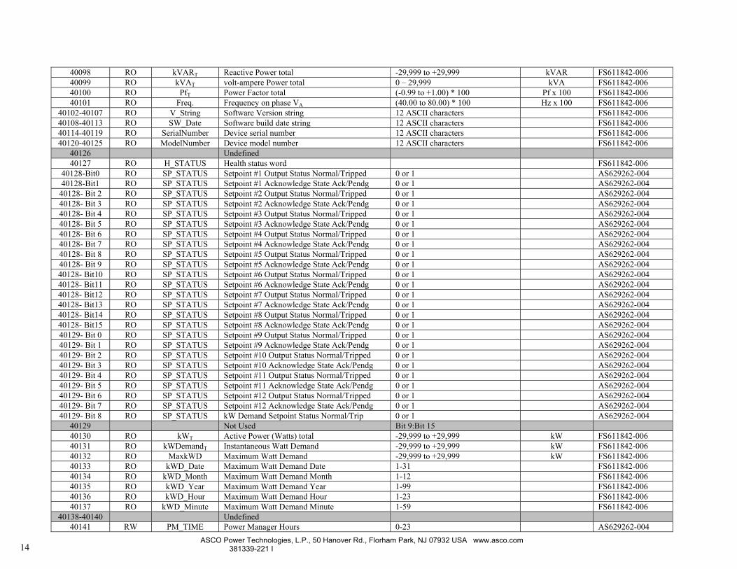
40098 RO kVART Reactive Power total -29,999 to +29,999 kVAR FS611842-00640099 RO kVAT volt-ampere Power total 0 – 29,999 kVA FS611842-00640100 RO PfT Power Factor total (-0.99 to +1.00) * 100 Pf x 100 FS611842-00640101 RO Freq. Frequency on phase VA (40.00 to 80.00) * 100 Hz x 100 FS611842-006
40102-40107 RO V_String Software Version string 12 ASCII characters FS611842-00640108-40113 RO SW_Date Software build date string 12 ASCII characters FS611842-00640114-40119 RO SerialNumber Device serial number 12 ASCII characters FS611842-00640120-40125 RO ModelNumber Device model number 12 ASCII characters FS611842-006
40126 Undefined40127 RO H_STATUS Health status word FS611842-006
40128-Bit0 RO SP_STATUS Setpoint #1 Output Status Normal/Tripped 0 or 1 AS629262-00440128-Bit1 RO SP_STATUS Setpoint #1 Acknowledge State Ack/Pendg 0 or 1 AS629262-004
40128- Bit 2 RO SP_STATUS Setpoint #2 Output Status Normal/Tripped 0 or 1 AS629262-00440128- Bit 3 RO SP_STATUS Setpoint #2 Acknowledge State Ack/Pendg 0 or 1 AS629262-00440128- Bit 4 RO SP_STATUS Setpoint #3 Output Status Normal/Tripped 0 or 1 AS629262-00440128- Bit 5 RO SP_STATUS Setpoint #3 Acknowledge State Ack/Pendg 0 or 1 AS629262-00440128- Bit 6 RO SP_STATUS Setpoint #4 Output Status Normal/Tripped 0 or 1 AS629262-00440128- Bit 7 RO SP_STATUS Setpoint #4 Acknowledge State Ack/Pendg 0 or 1 AS629262-00440128- Bit 8 RO SP_STATUS Setpoint #5 Output Status Normal/Tripped 0 or 1 AS629262-00440128- Bit 9 RO SP_STATUS Setpoint #5 Acknowledge State Ack/Pendg 0 or 1 AS629262-00440128- Bit10 RO SP_STATUS Setpoint #6 Output Status Normal/Tripped 0 or 1 AS629262-00440128- Bit11 RO SP_STATUS Setpoint #6 Acknowledge State Ack/Pendg 0 or 1 AS629262-00440128- Bit12 RO SP_STATUS Setpoint #7 Output Status Normal/Tripped 0 or 1 AS629262-00440128- Bit13 RO SP_STATUS Setpoint #7 Acknowledge State Ack/Pendg 0 or 1 AS629262-00440128- Bit14 RO SP_STATUS Setpoint #8 Output Status Normal/Tripped 0 or 1 AS629262-00440128- Bit15 RO SP_STATUS Setpoint #8 Acknowledge State Ack/Pendg 0 or 1 AS629262-00440129- Bit 0 RO SP_STATUS Setpoint #9 Output Status Normal/Tripped 0 or 1 AS629262-00440129- Bit 1 RO SP_STATUS Setpoint #9 Acknowledge State Ack/Pendg 0 or 1 AS629262-00440129- Bit 2 RO SP_STATUS Setpoint #10 Output Status Normal/Tripped 0 or 1 AS629262-00440129- Bit 3 RO SP_STATUS Setpoint #10 Acknowledge State Ack/Pendg 0 or 1 AS629262-00440129- Bit 4 RO SP_STATUS Setpoint #11 Output Status Normal/Tripped 0 or 1 AS629262-00440129- Bit 5 RO SP_STATUS Setpoint #11 Acknowledge State Ack/Pendg 0 or 1 AS629262-00440129- Bit 6 RO SP_STATUS Setpoint #12 Output Status Normal/Tripped 0 or 1 AS629262-00440129- Bit 7 RO SP_STATUS Setpoint #12 Acknowledge State Ack/Pendg 0 or 1 AS629262-00440129- Bit 8 RO SP_STATUS kW Demand Setpoint Status Normal/Trip 0 or 1 AS629262-004
40129 Not Used Bit 9:Bit 1540130 RO kWT Active Power (Watts) total -29,999 to +29,999 kW FS611842-00640131 RO kWDemandT Instantaneous Watt Demand -29,999 to +29,999 kW FS611842-00640132 RO MaxkWD Maximum Watt Demand -29,999 to +29,999 kW FS611842-00640133 RO kWD_Date Maximum Watt Demand Date 1-31 FS611842-00640134 RO kWD_Month Maximum Watt Demand Month 1-12 FS611842-00640135 RO kWD_Year Maximum Watt Demand Year 1-99 FS611842-00640136 RO kWD_Hour Maximum Watt Demand Hour 1-23 FS611842-00640137 RO kWD_Minute Maximum Watt Demand Minute 1-59 FS611842-006
40138-40140 Undefined40141 RW PM_TIME Power Manager Hours 0-23 AS629262-004
ASCO Power Technologies, L.P., 50 Hanover Rd., Florham Park, NJ 07932 USA www.asco.com 381339-221 I 15
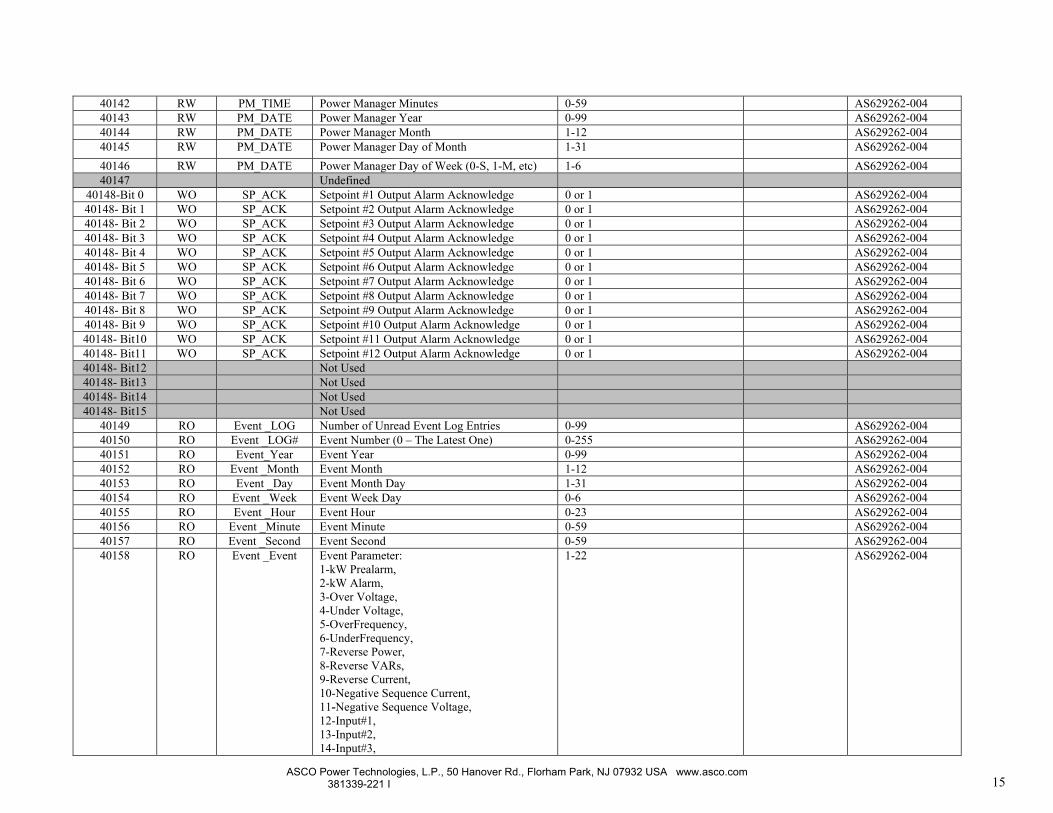
40142 RW PM_TIME Power Manager Minutes 0-59 AS629262-00440143 RW PM_DATE Power Manager Year 0-99 AS629262-00440144 RW PM_DATE Power Manager Month 1-12 AS629262-00440145 RW PM_DATE Power Manager Day of Month 1-31 AS629262-00440146 RW PM_DATE Power Manager Day of Week (0-S, 1-M, etc) 1-6 AS629262-00440147 Undefined
40148-Bit 0 WO SP_ACK Setpoint #1 Output Alarm Acknowledge 0 or 1 AS629262-00440148- Bit 1 WO SP_ACK Setpoint #2 Output Alarm Acknowledge 0 or 1 AS629262-00440148- Bit 2 WO SP_ACK Setpoint #3 Output Alarm Acknowledge 0 or 1 AS629262-00440148- Bit 3 WO SP_ACK Setpoint #4 Output Alarm Acknowledge 0 or 1 AS629262-00440148- Bit 4 WO SP_ACK Setpoint #5 Output Alarm Acknowledge 0 or 1 AS629262-00440148- Bit 5 WO SP_ACK Setpoint #6 Output Alarm Acknowledge 0 or 1 AS629262-00440148- Bit 6 WO SP_ACK Setpoint #7 Output Alarm Acknowledge 0 or 1 AS629262-00440148- Bit 7 WO SP_ACK Setpoint #8 Output Alarm Acknowledge 0 or 1 AS629262-00440148- Bit 8 WO SP_ACK Setpoint #9 Output Alarm Acknowledge 0 or 1 AS629262-00440148- Bit 9 WO SP_ACK Setpoint #10 Output Alarm Acknowledge 0 or 1 AS629262-00440148- Bit10 WO SP_ACK Setpoint #11 Output Alarm Acknowledge 0 or 1 AS629262-00440148- Bit11 WO SP_ACK Setpoint #12 Output Alarm Acknowledge 0 or 1 AS629262-00440148- Bit12 Not Used40148- Bit13 Not Used40148- Bit14 Not Used40148- Bit15 Not Used
40149 RO Event _LOG Number of Unread Event Log Entries 0-99 AS629262-00440150 RO Event _LOG# Event Number (0 – The Latest One) 0-255 AS629262-00440151 RO Event_Year Event Year 0-99 AS629262-00440152 RO Event _Month Event Month 1-12 AS629262-00440153 RO Event _Day Event Month Day 1-31 AS629262-00440154 RO Event _Week Event Week Day 0-6 AS629262-00440155 RO Event _Hour Event Hour 0-23 AS629262-00440156 RO Event _Minute Event Minute 0-59 AS629262-00440157 RO Event _Second Event Second 0-59 AS629262-00440158 RO Event _Event Event Parameter:
1-kW Prealarm,2-kW Alarm,3-Over Voltage,4-Under Voltage,5-OverFrequency,6-UnderFrequency,7-Reverse Power,8-Reverse VARs,9-Reverse Current,10-Negative Sequence Current,11-Negative Sequence Voltage,12-Input#1,13-Input#2,14-Input#3,
1-22 AS629262-004

ASCO Power Technologies, L.P., 50 Hanover Rd., Florham Park, NJ 07932 USA www.asco.com 381339-221 I16
15-Input#4,16-Input#5,17-Input#6,18-Input#7,19-Input#8,20-Input#9(switch position),21-None,22-KW Demand
40159 RO Event _Cause Event Cause: 0-Reset, 1-Tripped, 2-Acknowled 0-2 AS629262-00440160-Bit 0 RW DEVICE86 Device 86 Active? 0-No or 1-Yes AS629262-00440160-Bit 1 RW DEVICE86 Device 86 State 0-No or 1-Tripped AS629262-00440160-Bit 2 RW DEVICE86 Device 86 Hold 0-Reset Ok or 1-Do Not Reset AS629262-004
40161-40199 Undefined40200 RW TYPESYSTEM System Type FS611842-00640201 RW MODESOURCE Source Mode FS611842-00640202 RW PTR Potential Transformer Ratio FS611842-00640203 RW CTR Current Transformer Ratio FS611842-00640204 RW CT4R 4th Current Input Transformer Ratio FS611842-00640205 RW PROTOCOLSCI SCI comm. port (J5) protocol FS611842-00640206 RW BAUDSCI SCI comm. port (J5) baud rate FS611842-00640207 RW ADDRSCI SCI comm. port (J5) device address FS611842-00640208 RW PROTOCOL485 485 comm. port (J1) protocol FS611842-00640209 RW BAUD485 485 comm. port (J1) baud rate FS611842-00640210 RW ADDR485 485 comm. port (J1) device address FS611842-00640211 RW TYPELANG Language selection FS611842-00640212 RW Window_Size Demand Window size (in minutes) min. FS611842-00640213 RW Subintl_Size Demand Subinterval size (fixed at 1 minute) min. FS611842-00640214 WO Reset_Demand Resets Inst. & Max. demand registers FS611842-00640215 WO Clear_Energy Clears Energy registers to 0 FS611842-006
40216-40229 Undefined40230-40235 RW SETPOINT Setpoint configuration settings40236-40242
402364023740238402394024040241
40242-Bit0-340242-Bit 440242-Bit 540242-Bit 640242-Bit 7
RWRWRWRWRWRWRWRWRWRWRWRW
SETPOINT1#I
ParameterHigh_limit
TD_OperateLow_LimitTD_Release
Output--------
Setpoint#1 Configuration Settings:Setpoint NumberSetpoint ParameterSetpoint Trip LevelSetpoint Trip Time DelaySetpoint Reset LevelSetpoint Reset Time DelaySetpoint Digital Output :DO1 To DO4Output No Acknowledg/AcknowledgOutput Status Normal/TrippedPrevious Acknowledge/PendingPresent Acknowledge/Pending
0-110-200-5000-6000-5000-6000 or 10 or 10 or 10 or 10 or 1
AS629262-004
40243-40249 RW SETPOINT2 Setpoint#2 Configuration Settings Same Setting as SP#1 AS629262-00440250-40256 RW SETPOINT3 Setpoint#3 Configuration Settings Same Setting as SP #1 AS629262-00440257-40263 RW SETPOINT4 Setpoint#4 Configuration Settings Same Setting as SP #1 AS629262-00440264-40270 RW SETPOINT5 Setpoint#5 Configuration Settings Same Setting as SP #1 AS629262-004

ASCO Power Technologies, L.P., 50 Hanover Rd., Florham Park, NJ 07932 USA www.asco.com 381339-221 I 17
40271-40277 RW SETPOINT6 Setpoint#6 Configuration Settings Same Setting as SP #1 AS629262-00440278-40284 RW SETPOINT7 Setpoint#7 Configuration Settings Same Setting as SP #1 AS629262-00440285-40291 RW SETPOINT8 Setpoint#8 Configuration Settings Same Setting as SP #1 AS629262-00440292-40298 RW SETPOINT9 Setpoint#9 Configuration Settings Same Setting as SP #1 AS629262-00440299-40305 RW SETPOINT10 Setpoint#10 Configuration Settings Same Setting as SP #1 AS629262-00440306-40312 RW SETPOINT11 Setpoint#11 Configuration Settings Same Setting as SP #1 AS629262-00440313-40319 RW SETPOINT12 Setpoint#12 Configuration Settings Same Setting as SP #1 AS629262-00440320-40321 Undefined40322-40325 RW PM-Name Power Manager Name 8 ASCII chars AS629262-00440326-40333 RW Status1_Name S1 Status Input name 15 chars+ 1 byte eng. alarms FS611842-00640334-40341 RW Status2_Name S2 Status Input name 15 chars+ 1 byte eng. alarms FS611842-00640342-40349 RW Status3_Name S3 Status Input name 15 chars+ 1 byte eng. alarms FS611842-00640350-40357 RW Status4_Name S4 Status Input name 15 chars+ 1 byte eng. alarms FS611842-00640358-40365 RW Status5_Name S5 Status Input name 15 chars+ 1 byte eng. alarms FS611842-00640366-40373 RW Status6_Name S6 Status Input name 15 chars+ 1 byte eng. alarms FS611842-00640374-40381 RW Status7_Name S7 Status Input name 15 chars+ 1 byte eng. alarms FS611842-00640382-40389 RW Status8_Name S8 Status Input name 15 chars+ 1 byte eng. alarms FS611842-00640390-40397 RW Relay1_Name DO1 Relay Output name 15 chars+ 1 byte eng. alarms FS611842-00640398-40405 RW Relay2_Name DO2 Relay Output name 15 chars+ 1 byte eng. alarms FS611842-00640406-40413 RW Relay3_Name DO3 Relay Output name 15 chars+ 1 byte eng. alarms FS611842-00640414-40421 RW Relay4_Name DO4 Relay Output name 15 chars+ 1 byte eng. alarms FS611842-00640422-40431 RW PM-Location Power Manager Location 20 ASCII chars AS629262-004
40432 Undefined

ASCO Power Technologies, L.P., 50 Hanover Rd., Florham Park, NJ 07932 USA www.asco.com 381339-221 I18
Register Map for Group 5 ControllerThe following table describes the mapping of the registers within the Group 5 Controller to Holding Registers defined in the Modbus protocol.
Note: The addresses in the format of 4xxxx follow the MODICON MODBUS protocol for point addressing.The actual address sent is the Register Address shown in the map minus the value 40001.
Real Time Data RegistersRegisterAddress
RegisterType
ParameterName
ParameterDescription
Data Range Units Implemented inFirmware Version
40001- 40011 Undefined40012 RO PHASE_0 Phase Shift between Normal & Emergency -1800 – 1800 deg x 10 607540-02340013 RO NFRQ_0 Normal Frequency 0 – 7000 Hz x 100 607540-02340014 RO EFRQ_0 Emergency Frequency 0 – 7000 Hz x 100 607540-023
40015-Bit 0 RO I_MAIN_ON_N Main on Normal Boolean 607540-02340015-Bit 1 RO I_MAIN_ON_E Main on Emergency Boolean 607540-02340015-Bit 2 RO I_AUX_ON_N Auxiliary on Normal Boolean 607540-02340015-Bit 3 RO I_AUX_ON_E Auxiliary on Emergency Boolean 607540-02340015-Bit 4 RO N.SrcAvl Normal Source Available Boolean 607540-02340015-Bit 5 RO E.SrcAvl Emergency Source Available Boolean 607540-02340016-Bit 0 RO STATPHR.NABC Normal Phase Rotation is ABC Boolean 607540-02340016-Bit 1 RO STATPHR.NCBA Normal Phase Rotation is CBA Boolean 607540-02340016-Bit 2 RO STATPHR.EABC Emergency Phase Rotation is ABC Boolean 607540-02340016-Bit 3 RO STATPHR.ECBA Emergency Phase Rotation is CBA Boolean 607540-02340016-Bit 4 RO XRQ_F11C_LX Engine Exerciser with Load Active Boolean 607540-02340016-Bit 5 RO not used not used Boolean 607540-02340016-Bit 6 RO I_F17_ON External F17 is Active Boolean 607540-023
40017 RO NV_AB Normal Voltage Phase AB 0 to 28200 Volt 607540-02340018 RO NV_BC Normal Voltage Phase BC 0 to 28200 Volt 607540-02340019 RO NV_CA Normal Voltage Phase CA 0 to 28200 Volt 607540-02340020 RO NVUnblCur Normal Voltage Unbalance 0 to 99 % Volt 607540-02340021 RO EV_AB Emergency Voltage Phase AB 0 to 28200 Volt 607540-02340022 RO EV_BC Emergency Voltage Phase BC 0 to 28200 Volt 607540-02340023 RO EV_CA Emergency Voltage Phase CA 0 to 28200 Volt 607540-02340024 RO EVUnblCur Emergency Voltage Unbalance 0 to 99 % Volt 607540-02340025 RO I_NOM_V Nominal Voltage 0 to 15 (Note 1) Volt 607540-023
40026-Bit 0 RO I_FRQ_60 Nominal Frequency Bool (60-50 Hz) 607540-02340026-Bit 1 RO I_N3PHASE Normal Source 3 Phase sensing Boolean 607540-02340026-Bit 2 RO I_E3PHASE Emergency Source 3 Phase sensing Boolean 607540-023
40026-Bit3-4 RO TSType Transfer Switch Type (CTTS, OTTS,DTTS) 0 to 3 (Note 2) 607540-02340026-Bit 5 RO TSBypass Transfer Switch Bypass or not Boolean 607540-02340026-Bit 6 RO ATS/DualBreaker Transfer Switch or Dual Breaker Boolean 607540-033
40027 RO TSAmp Transfer Switch Amp rating 0 to 15 (Note 3) 607540-02340028-40033 RO LCD_CP_VER Control Panel Software version 10 char. string 607540-02340034-40039 RO LCD_CP_DATE Control Panel Software date 10 char. string 607540-02340040-Bit 0 RO OPSave.b.ATSLout Transfer Switch Locked Out Boolean 607540-023
ASCO Power Technologies, L.P., 50 Hanover Rd., Florham Park, NJ 07932 USA www.asco.com 381339-221 I 19
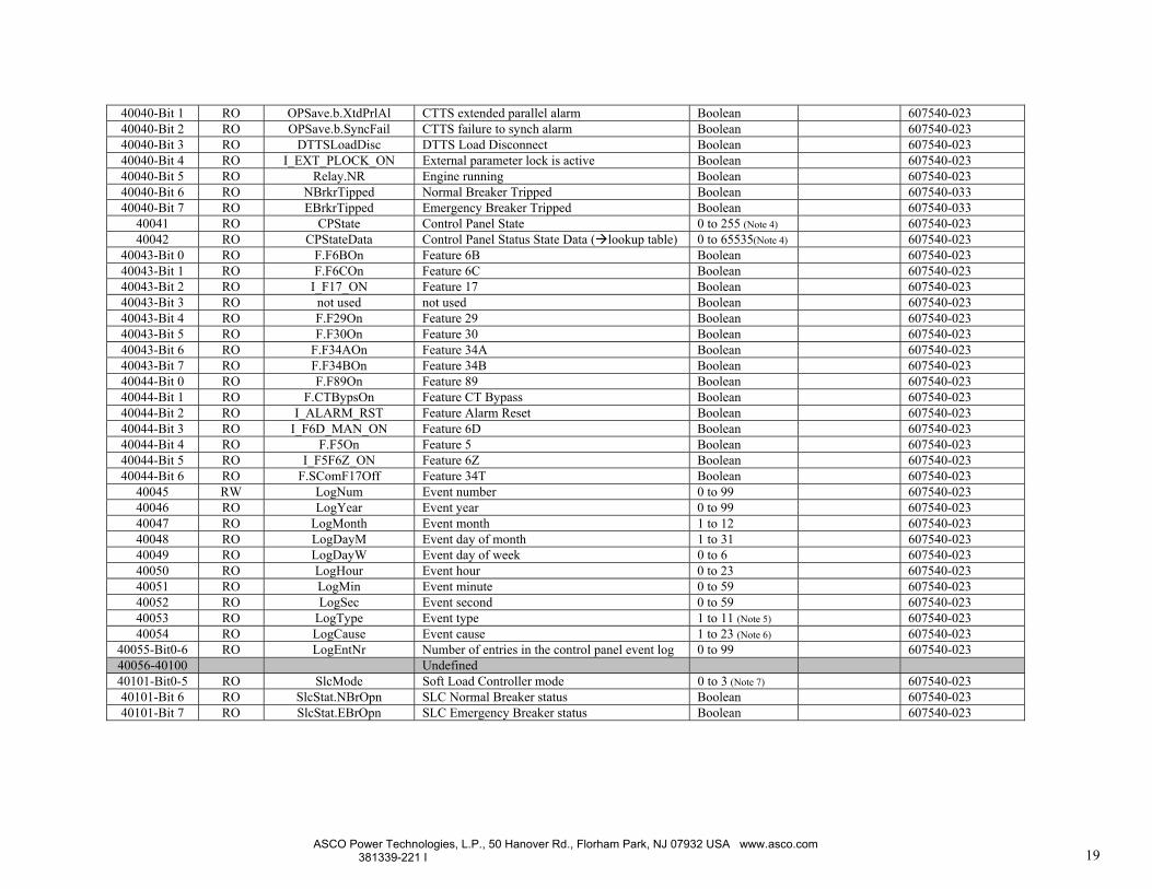
40040-Bit 1 RO OPSave.b.XtdPrlAl CTTS extended parallel alarm Boolean 607540-02340040-Bit 2 RO OPSave.b.SyncFail CTTS failure to synch alarm Boolean 607540-02340040-Bit 3 RO DTTSLoadDisc DTTS Load Disconnect Boolean 607540-02340040-Bit 4 RO I_EXT_PLOCK_ON External parameter lock is active Boolean 607540-02340040-Bit 5 RO Relay.NR Engine running Boolean 607540-02340040-Bit 6 RO NBrkrTipped Normal Breaker Tripped Boolean 607540-03340040-Bit 7 RO EBrkrTipped Emergency Breaker Tripped Boolean 607540-033
40041 RO CPState Control Panel State 0 to 255 (Note 4) 607540-02340042 RO CPStateData Control Panel Status State Data ( lookup table) 0 to 65535(Note 4) 607540-023
40043-Bit 0 RO F.F6BOn Feature 6B Boolean 607540-02340043-Bit 1 RO F.F6COn Feature 6C Boolean 607540-02340043-Bit 2 RO I_F17_ON Feature 17 Boolean 607540-02340043-Bit 3 RO not used not used Boolean 607540-02340043-Bit 4 RO F.F29On Feature 29 Boolean 607540-02340043-Bit 5 RO F.F30On Feature 30 Boolean 607540-02340043-Bit 6 RO F.F34AOn Feature 34A Boolean 607540-02340043-Bit 7 RO F.F34BOn Feature 34B Boolean 607540-02340044-Bit 0 RO F.F89On Feature 89 Boolean 607540-02340044-Bit 1 RO F.CTBypsOn Feature CT Bypass Boolean 607540-02340044-Bit 2 RO I_ALARM_RST Feature Alarm Reset Boolean 607540-02340044-Bit 3 RO I_F6D_MAN_ON Feature 6D Boolean 607540-02340044-Bit 4 RO F.F5On Feature 5 Boolean 607540-02340044-Bit 5 RO I_F5F6Z_ON Feature 6Z Boolean 607540-02340044-Bit 6 RO F.SComF17Off Feature 34T Boolean 607540-023
40045 RW LogNum Event number 0 to 99 607540-02340046 RO LogYear Event year 0 to 99 607540-02340047 RO LogMonth Event month 1 to 12 607540-02340048 RO LogDayM Event day of month 1 to 31 607540-02340049 RO LogDayW Event day of week 0 to 6 607540-02340050 RO LogHour Event hour 0 to 23 607540-02340051 RO LogMin Event minute 0 to 59 607540-02340052 RO LogSec Event second 0 to 59 607540-02340053 RO LogType Event type 1 to 11 (Note 5) 607540-02340054 RO LogCause Event cause 1 to 23 (Note 6) 607540-023
40055-Bit0-6 RO LogEntNr Number of entries in the control panel event log 0 to 99 607540-02340056-40100 Undefined40101-Bit0-5 RO SlcMode Soft Load Controller mode 0 to 3 (Note 7) 607540-02340101-Bit 6 RO SlcStat.NBrOpn SLC Normal Breaker status Boolean 607540-02340101-Bit 7 RO SlcStat.EBrOpn SLC Emergency Breaker status Boolean 607540-023

ASCO Power Technologies, L.P., 50 Hanover Rd., Florham Park, NJ 07932 USA www.asco.comModbus is a registered trademark of Gould Inc. 1 381339-221 I
Note 1
Nominal Voltage
Data Voltage0 115V1 120V2 208V3 220V4 230V5 240V6 277V7 380V8 400V9 415V
10 440V11 460V12 480V13 550V14 575V15 600V
Note 2
Switch Type
Data Switch Type0 OTTS1 DTTS2 CTTS3 OTTS
Note 7
SLC Mode
Data SLC Mode0 No SLC1 Islanding2 Parallel Base Load3 Import/Export
Note 3
Switch Amp Rating
Data Amp Rating0 30A1 70A2 100A3 150A4 260A5 400A6 600A7 800A8 1000A9 1200A
10 1600A11 2000A12 3000A13 4000A14 OTHER15 OTHER
Note 5
Event Type
Data Event Type1 Engine Start2 Transfer N>E3 Transfer E>N4 Engine Stop5 Emerg Acceptable6 Emerg Not Accept.7 Normal Acceptable8 Normal Not Accept.9 Transfer Abort10 Breaker Trip11 YY Primary Fail
Note 6
Event Cause
Data Event Cause1 Load Shed2 Normal Fail3 Manual Transfer4 Test 55 Test 176 Communication7 Engine Exerciser8 Emergency Fail9 Normal Under Voltage10 Normal Over Voltage11 Normal Under Frequency12 Normal Over Frequency13 Normal Phase Rotation14 Normal Voltage Unbal.15 Emerg. Under Voltage16 Emerg. Over Voltage17 Emerg. Under Frequency18 Emerg. Over Frequency19 Emerg. Phase Rotation20 Emerg. Voltage Unbal.21 Feature 622 Normal Breaker23 Emergency Breaker
ASCO Power Technologies, L.P., 50 Hanover Rd., Florham Park, NJ 07932 USA www.asco.comModbus is a registered trademark of Gould Inc. 1 381339-221 I
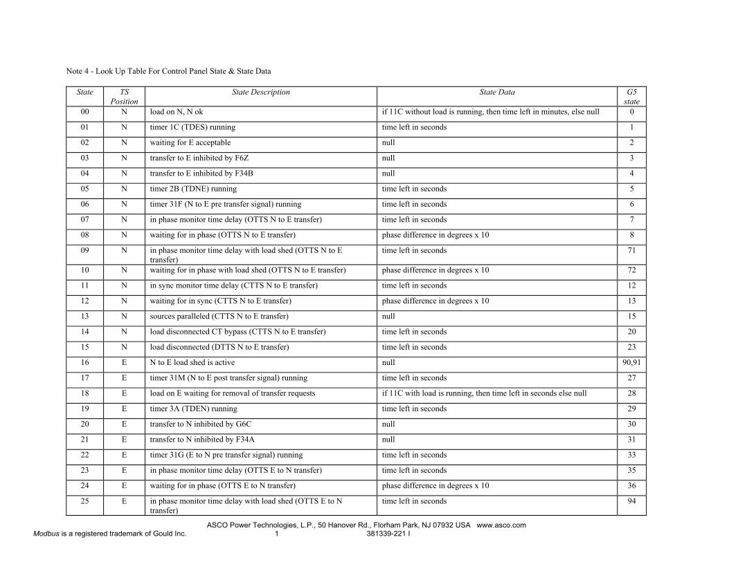
Note 4 - Look Up Table For Control Panel State & State Data
State TSPosition
State Description State Data G5state
00 N load on N, N ok if 11C without load is running, then time left in minutes, else null 0
01 N timer 1C (TDES) running time left in seconds 1
02 N waiting for E acceptable null 2
03 N transfer to E inhibited by F6Z null 3
04 N transfer to E inhibited by F34B null 4
05 N timer 2B (TDNE) running time left in seconds 5
06 N timer 31F (N to E pre transfer signal) running time left in seconds 6
07 N in phase monitor time delay (OTTS N to E transfer) time left in seconds 7
08 N waiting for in phase (OTTS N to E transfer) phase difference in degrees x 10 8
09 N in phase monitor time delay with load shed (OTTS N to Etransfer)
time left in seconds 71
10 N waiting for in phase with load shed (OTTS N to E transfer) phase difference in degrees x 10 72
11 N in sync monitor time delay (CTTS N to E transfer) time left in seconds 12
12 N waiting for in sync (CTTS N to E transfer) phase difference in degrees x 10 13
13 N sources paralleled (CTTS N to E transfer) null 15
14 N load disconnected CT bypass (CTTS N to E transfer) time left in seconds 20
15 N load disconnected (DTTS N to E transfer) time left in seconds 23
16 E N to E load shed is active null 90,91
17 E timer 31M (N to E post transfer signal) running time left in seconds 27
18 E load on E waiting for removal of transfer requests if 11C with load is running, then time left in seconds else null 28
19 E timer 3A (TDEN) running time left in seconds 29
20 E transfer to N inhibited by G6C null 30
21 E transfer to N inhibited by F34A null 31
22 E timer 31G (E to N pre transfer signal) running time left in seconds 33
23 E in phase monitor time delay (OTTS E to N transfer) time left in seconds 35
24 E waiting for in phase (OTTS E to N transfer) phase difference in degrees x 10 36
25 E in phase monitor time delay with load shed (OTTS E to Ntransfer)
time left in seconds 94
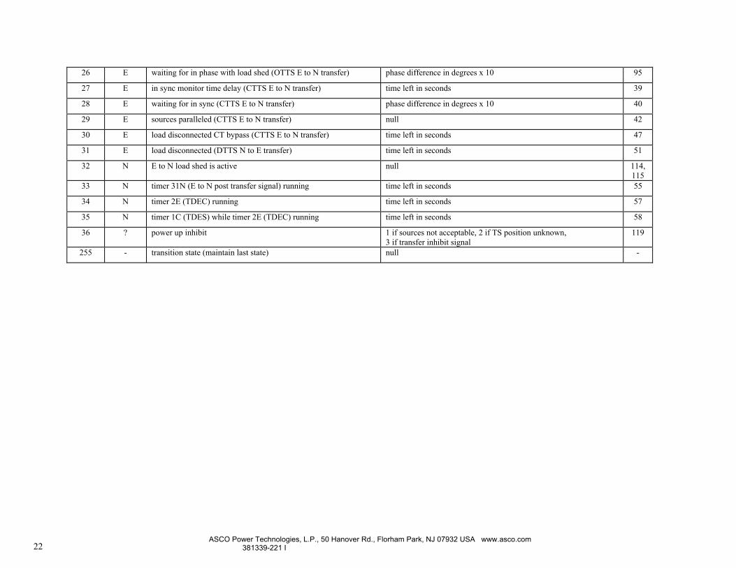
ASCO Power Technologies, L.P., 50 Hanover Rd., Florham Park, NJ 07932 USA www.asco.com 381339-221 I22
26 E waiting for in phase with load shed (OTTS E to N transfer) phase difference in degrees x 10 95
27 E in sync monitor time delay (CTTS E to N transfer) time left in seconds 39
28 E waiting for in sync (CTTS E to N transfer) phase difference in degrees x 10 40
29 E sources paralleled (CTTS E to N transfer) null 42
30 E load disconnected CT bypass (CTTS E to N transfer) time left in seconds 47
31 E load disconnected (DTTS N to E transfer) time left in seconds 51
32 N E to N load shed is active null 114,115
33 N timer 31N (E to N post transfer signal) running time left in seconds 55
34 N timer 2E (TDEC) running time left in seconds 57
35 N timer 1C (TDES) while timer 2E (TDEC) running time left in seconds 58
36 ? power up inhibit 1 if sources not acceptable, 2 if TS position unknown,3 if transfer inhibit signal
119
255 - transition state (maintain last state) null -