compensation design for peak current-mode buck converters/media/an pdf/an028_en.pdf · compensation...
TRANSCRIPT
Application Note
李彥德 AN028 – Apr 2014
AN028 © 2014 Richtek Technology Corporation 1
Compensation Design for Peak Current-Mode Buck Converters
Abstract
Peak Current-Mode Controlled Buck Converters are currently very popular and widely adopted in consumer electronics and
computer peripheral power management. This application note presents a design procedure for feedback compensation of peak
current-mode buck converters, and also introduces the SIMPLIS tool for circuit simulations and the Mathcad mathematical
software for quantitative design, and finally provides the verified results by actual measurements.
Contents
1. Open-Loop Analysis of Peak Current Mode Buck Converters ...................................................................2
2. Compensation Design of Peak Current-Mode Buck Converters ................................................................7
3. The Closed-Loop Analysis of Peak Current-Mode Buck Converters ........................................................ 11
4. Conclusion ............................................................................................................................................. 13
5. References ............................................................................................................................................ 13
Compensation Design for
Peak Current-Mode Buck Converters
AN028 © 2014 Richtek Technology Corporation 2
1. Open-Loop Analysis of Peak Current Mode Buck Converters
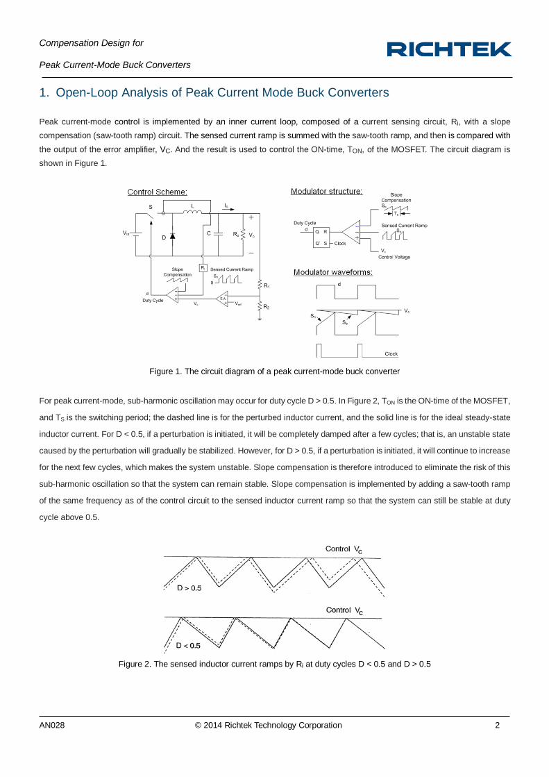
Peak current-mode control is implemented by an inner current loop, composed of a current sensing circuit, Ri, with a slope
compensation (saw-tooth ramp) circuit. The sensed current ramp is summed with the saw-tooth ramp, and then is compared with
the output of the error amplifier, VC. And the result is used to control the ON-time, TON, of the MOSFET. The circuit diagram is
shown in Figure 1.
Figure 1. The circuit diagram of a peak current-mode buck converter
For peak current-mode, sub-harmonic oscillation may occur for duty cycle D > 0.5. In Figure 2, TON is the ON-time of the MOSFET,
and TS is the switching period; the dashed line is for the perturbed inductor current, and the solid line is for the ideal steady-state
inductor current. For D < 0.5, if a perturbation is initiated, it will be completely damped after a few cycles; that is, an unstable state
caused by the perturbation will gradually be stabilized. However, for D > 0.5, if a perturbation is initiated, it will continue to increase
for the next few cycles, which makes the system unstable. Slope compensation is therefore introduced to eliminate the risk of this
sub-harmonic oscillation so that the system can remain stable. Slope compensation is implemented by adding a saw-tooth ramp
of the same frequency as of the control circuit to the sensed inductor current ramp so that the system can still be stable at duty
cycle above 0.5.
Figure 2. The sensed inductor current ramps by Ri at duty cycles D < 0.5 and D > 0.5
Compensation Design for
Peak Current-Mode Buck Converters
AN028 © 2014 Richtek Technology Corporation 3
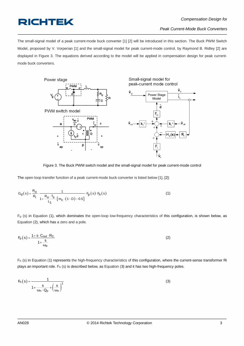
The small-signal model of a peak current-mode buck converter [1] [2] will be introduced in this section. The Buck PWM Switch
Model, proposed by V. Vorperian [1] and the small-signal model for peak current-mode control, by Raymond B. Ridley [2] are
displayed in Figure 3. The equations derived according to the model will be applied in compensation design for peak current-
mode buck converters.
Figure 3. The Buck PWM switch model and the small-signal model for peak current-mode control
The open-loop transfer function of a peak current-mode buck converter is listed below [1], [2]:
R 1oG s F s F sd p h
R R Ti o s1 m 1 D 0.5c
L1
(1)
Fp (s) in Equation (1), which dominates the open-loop low-frequency characteristics of this configuration, is shown below, as
Equation (2), which has a zero and a pole.
out Cp
p
1 s C RF s
s1ω
(2)
Fh (s) in Equation (1) represents the high-frequency characteristics of this configuration, where the current-sense transformer Ri
plays an important role. Fh (s) is described below, as Equation (3) and it has two high-frequency poles.
h
2
n p n
1F s
s s1ω Q ω
(3)
Compensation Design for
Peak Current-Mode Buck Converters
AN028 © 2014 Richtek Technology Corporation 4
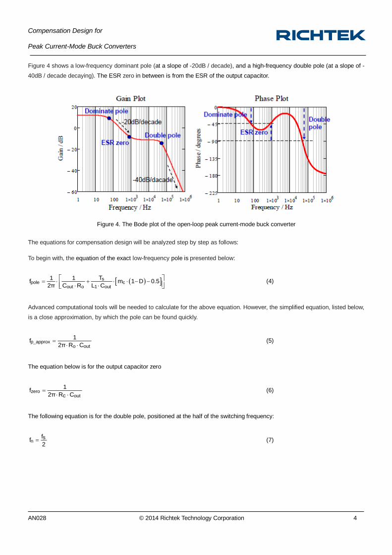
Figure 4 shows a low-frequency dominant pole (at a slope of -20dB / decade), and a high-frequency double pole (at a slope of -
40dB / decade decaying). The ESR zero in between is from the ESR of the output capacitor.
Figure 4. The Bode plot of the open-loop peak current-mode buck converter
The equations for compensation design will be analyzed step by step as follows:
To begin with, the equation of the exact low-frequency pole is presented below:
spole c
out o 1 out
T1 1f m 1 D 0.5
2π C R L C
(4)
Advanced computational tools will be needed to calculate for the above equation. However, the simplified equation, listed below,
is a close approximation, by which the pole can be found quickly.
p_approxo out
1f
2π R C
(5)
The equation below is for the output capacitor zero
zerooutc
1f
2π R C
(6)
The following equation is for the double pole, positioned at the half of the switching frequency:
nsff2
(7)
Compensation Design for
Peak Current-Mode Buck Converters
AN028 © 2014 Richtek Technology Corporation 5
With the equations above, a design example will be offered to describe the important characteristics of a peak current-mode buck
converter.
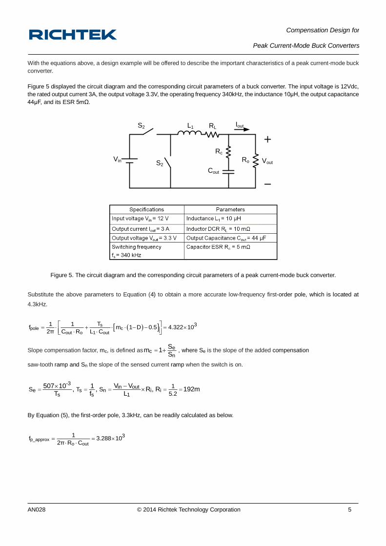
Figure 5 displayed the circuit diagram and the corresponding circuit parameters of a buck converter. The input voltage is 12Vdc,
the rated output current 3A, the output voltage 3.3V, the operating frequency 340kHz, the inductance 10μH, the output capacitance
44μF, and its ESR 5mΩ.
Figure 5. The circuit diagram and the corresponding circuit parameters of a peak current-mode buck converter.
Substitute the above parameters to Equation (4) to obtain a more accurate low-frequency first-order pole, which is located at
4.3kHz.
spole c
out o 1 out
3T1 1f m 1 D 0.5 4.322 10
2π C R L C
Slope compensation factor, mc, is defined as ec
n
Sm 1
S , where Se is the slope of the added compensation
saw-tooth ramp and Sn the slope of the sensed current ramp when the switch is on.
-3in out
e s n i is s 1
1S T S
5.2
V V507 10 1, , R , R 192m
T f L
By Equation (5), the first-order pole, 3.3kHz, can be readily calculated as below.
p_approxo out
31f 3.288 10
2π R C
L1
Cout
Vin Vout
Iout
Ro
Rc
RL
S2
S2
Compensation Design for
Peak Current-Mode Buck Converters
AN028 © 2014 Richtek Technology Corporation 6
Substitute the above parameters to Equation (6), and the exact location of the output capacitor ESR zero can be found as 723kHz.
zeroout
3
c
1f 723.432 10
2π R C
Then, by Equation (7), the high-frequency double pole is obtained as 170kHz.
n3sff 170 10
2
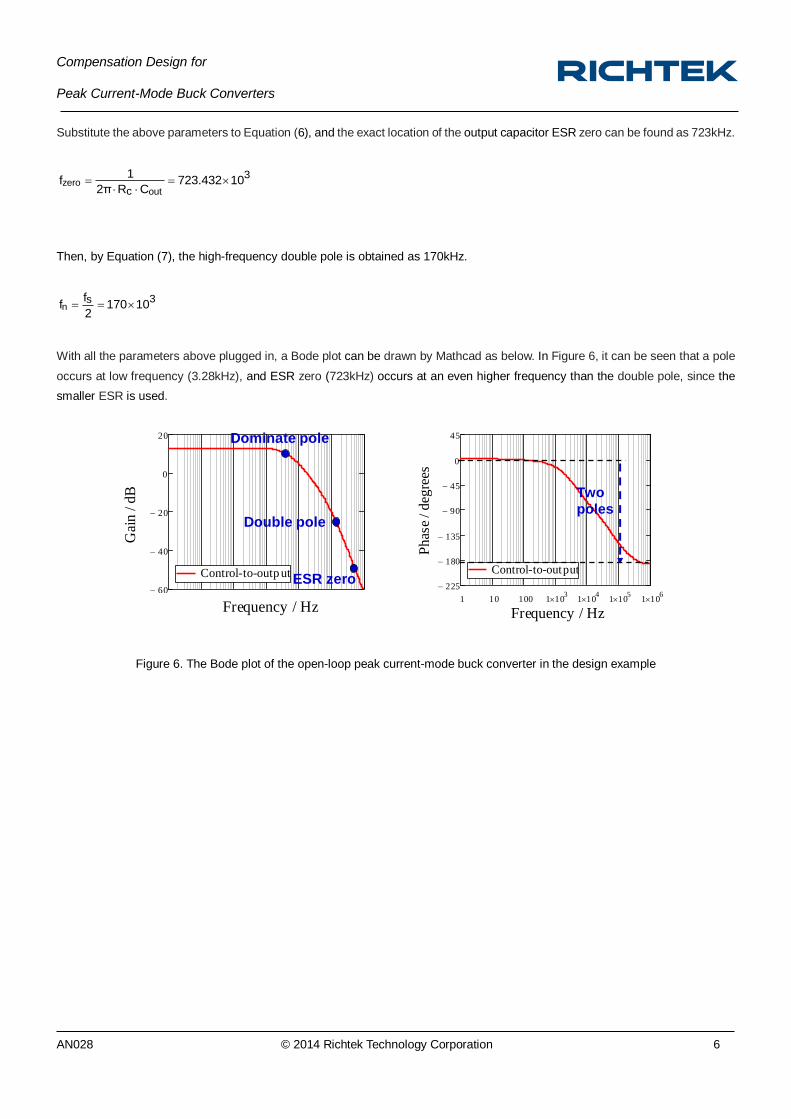
With all the parameters above plugged in, a Bode plot can be drawn by Mathcad as below. In Figure 6, it can be seen that a pole
occurs at low frequency (3.28kHz), and ESR zero (723kHz) occurs at an even higher frequency than the double pole, since the
smaller ESR is used.
Figure 6. The Bode plot of the open-loop peak current-mode buck converter in the design example
1 10 100 1 103
1 104
1 105
1 106
60
40
20
0
20
Control-to-outp ut
Gain Plot
Frequency / Hz
Gai
n /
dB
1 10 100 1 103
1 104
1 105
1 106
60
40
20
0
20
Gain Plot
Frequency / Hz
Gai
n / d
B
1 10 100 1 103
1 104
1 105
1 106
60
40
20
0
20
Gain Plot
Frequency / Hz
Gai
n /
dB Dominate pole
ESR zero
Double pole
1 10 100 1 103
1 104
1 105
1 106
60
40
20
0
20
Gain Plot
Frequency / Hz
Gai
n /
dB
1 10 100 1 103
1 104
1 105
1 106
225
180
135
90
45
0
45
90
135
180
225
Control-to-output
Phase Plot
Frequency / Hz
Phas
e /
deg
rees
1 10 100 1 103
1 104
1 105
1 106
225
180
135
90
45
0
45
Control-to-output
Phase Plot
Frequency / Hz
Phas
e / deg
rees
Two
poles
Compensation Design for
Peak Current-Mode Buck Converters
AN028 © 2014 Richtek Technology Corporation 7
2. Compensation Design of Peak Current-Mode Buck Converters
The previous section has described the characteristics of a peak current-mode buck. In this section, how to compensate peak
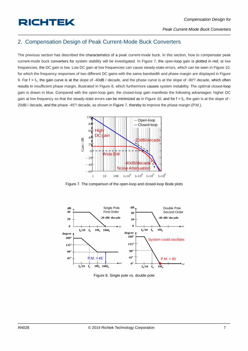
current-mode buck converters for system stability will be investigated. In Figure 7, the open-loop gain is plotted in red; at low
frequencies, the DC gain is low. Low DC gain at low frequencies can cause steady-state errors, which can be seen in Figure 10,
for which the frequency responses of two different DC gains with the same bandwidth and phase margin are displayed in Figure
9. For f > fc, the gain curve is at the slope of -40dB / decade, and the phase curve is at the slope of -90°/ decade, which often
results in insufficient phase margin, illustrated in Figure 8, which furthermore causes system instability. The optimal closed-loop
gain is drawn in blue. Compared with the open-loop gain, the closed-loop gain manifests the following advantages: higher DC
gain at low frequency so that the steady-state errors can be minimized as in Figure 10, and for f > fc, the gain is at the slope of -
20dB / decade, and the phase -45°/ decade, as shown in Figure 7, thereby to improve the phase margin (P.M.).
Figure 7. The comparison of the open-loop and closed-loop Bode plots
Figure 8. Single pole vs. double pole
1 10 100 1 103
1 104
1 105
1 106
60
40
20
0
20
40
60
80
100
Gain Plot
Frequency / Hz
Gai
n /
dB
1 10 100 1 103
1 104
1 105
1 106
60
40
20
0
20
40
Gain Plot
Frequency / Hz
Gai
n /
dB -20dB/decade
High
DC gain
Wide BW
-40dB/decade
Noise Attenuation
─ Open-loop
─ Closed-loop
ω
dB
-20 dB/ decade
ω
degree
40
20
0
180°
135o
90o
45o
fp 10fpfp/10
fp 10fpfp/10
100fp
100fp
ω
dB
-40 dB/ decade
ω
degree
40
20
0
0°
90o
fp
180o
135o
45o
10fpfp/10
fp 10fpfp/10
P.M. > 45° P.M. < 45°
System could oscillate.
Single Pole
First OrderDouble Pole
Second Order
Compensation Design for
Peak Current-Mode Buck Converters
AN028 © 2014 Richtek Technology Corporation 8
Figure 9. Different DC gains with the same bandwidth and phase margin
In Figure 10, it can be seen load regulation is better with higher DC gain, and worse with lower DC gain.
Figure 10. The effect of DC gains on load regulation
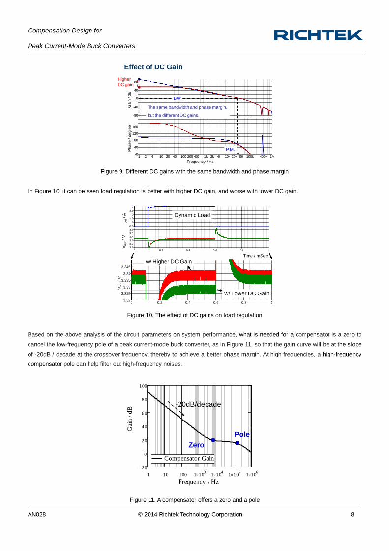
Based on the above analysis of the circuit parameters on system performance, what is needed for a compensator is a zero to
cancel the low-frequency pole of a peak current-mode buck converter, as in Figure 11, so that the gain curve will be at the slope
of -20dB / decade at the crossover frequency, thereby to achieve a better phase margin. At high frequencies, a high-frequency
compensator pole can help filter out high-frequency noises.
Figure 11. A compensator offers a zero and a pole
Higher
DC gain
Gain
(Loop G
ain
) /
-80
-40
0
40
80
freq / Hertz
1 2 4 10 20 40 100 200 400 1k 2k 4k 10k 20k 40k 100k 400k 1MPhase(L
oop G
ain
) /
degre
es
-0
40
80
120
160
Effect of DC Gain
The same bandwidth and phase margin,
but the different DC gains.
BW
P.M.Phase /
degre
eG
ain
/ d
B
Frequency / Hz
I(S
3-P
) /
A
0.5
1
1.5
2
2.5
3
time/mSecs 200uSecs/div
0 0.2 0.4 0.6 0.8 1
Vout
/ V
3.32
3.325
3.33
3.335
3.34
3.345
I(S
3-P
) /
A
0.5
1
1.5
2
2.5
3
time/mSecs 200uSecs/div
0 0.2 0.4 0.6 0.8 1
Vout
/ V
3.1
3.2
3.3
3.4
3.5
3.6
Vo
ut/
VI o
ut/ A Dynamic Load
w/ Higher DC Gain
w/ Lower DC Gain
Time / mSec
Vo
ut/
V
1 10 100 1 103
1 104
1 105
1 106
60
40
20
0
20
40
60
80
100
120
Control-to-Output
Loop Gain
Control-to-Output Gain
Frequency / Hz
Gai
n / d
B
1 10 100 1 103
1 104
1 105
1 106
20
0
20
40
60
80
100
Compendator Gain
Compendator Gain
Frequency / Hz
Gai
n / d
B
1 10 100 1 103
1 104
1 105
1 106
60
40
20
0
20
40
60
80
100
120
Control-to-Output
Loop Gain
Control-to-Output Gain
Frequency / Hz
Gai
n / d
B
1 10 100 1 103
1 104
1 105
1 106
20
0
20
40
60
80
100
Compendator Gain
Compendator Gain
Frequency / Hz
Gai
n / d
B
1 10 100 1 103
1 104
1 105
1 106
60
40
20
0
20
40
60
80
100
Control-to-Outp ut
Loop Gain
Control-to-Output Gain
Frequency / Hz
Gai
n /
dB
1 10 100 1 103
1 104
1 105
1 106
20
0
20
40
60
80
100
Compensator Gain
Compendator Gain
Frequency / Hz
Gai
n /
dB
-20dB/decade
Zero
Pole
Compensation Design for
Peak Current-Mode Buck Converters
AN028 © 2014 Richtek Technology Corporation 9
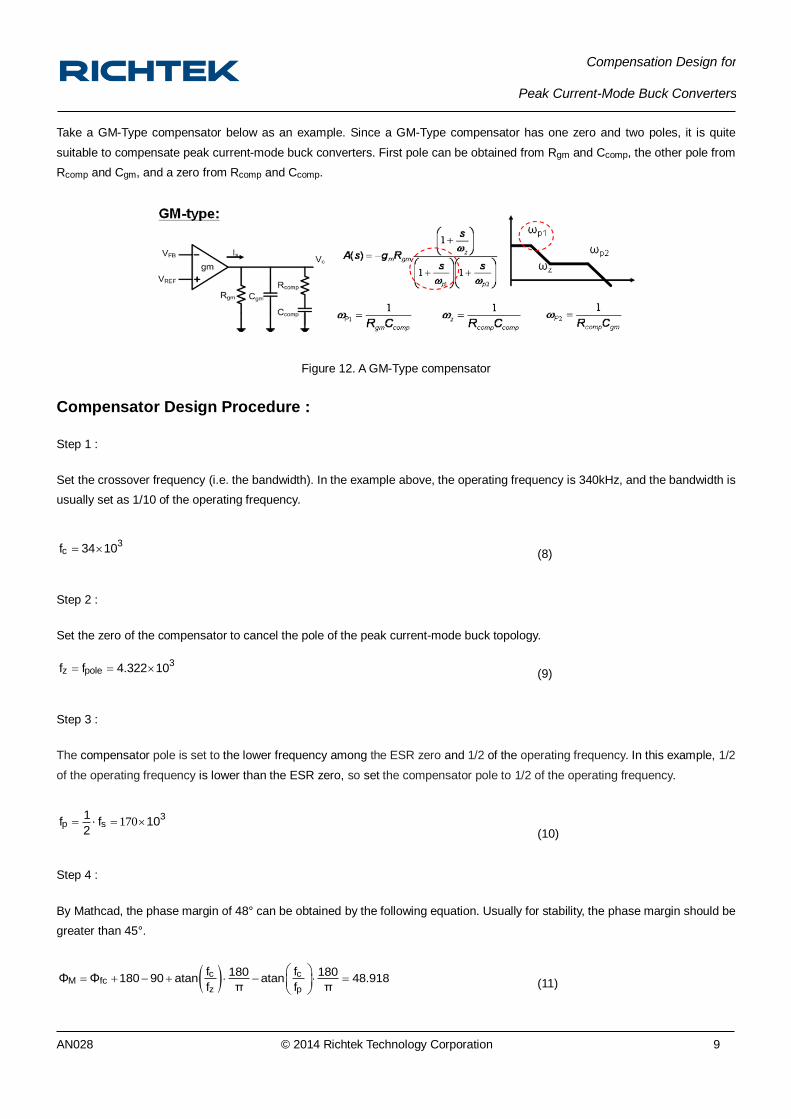
Take a GM-Type compensator below as an example. Since a GM-Type compensator has one zero and two poles, it is quite
suitable to compensate peak current-mode buck converters. First pole can be obtained from Rgm and Ccomp, the other pole from
Rcomp and Cgm, and a zero from Rcomp and Ccomp.
Figure 12. A GM-Type compensator
Compensator Design Procedure :
Step 1 :
Set the crossover frequency (i.e. the bandwidth). In the example above, the operating frequency is 340kHz, and the bandwidth is
usually set as 1/10 of the operating frequency.
3cf 34 10 (8)
Step 2 :
Set the zero of the compensator to cancel the pole of the peak current-mode buck topology.
3z polef f 4.322 10
(9)
Step 3 :
The compensator pole is set to the lower frequency among the ESR zero and 1/2 of the operating frequency. In this example, 1/2
of the operating frequency is lower than the ESR zero, so set the compensator pole to 1/2 of the operating frequency.
1703
p s1
f f 102
(10)
Step 4 :
By Mathcad, the phase margin of 48° can be obtained by the following equation. Usually for stability, the phase margin should be
greater than 45°.
c cM fc
z p
f f180 180Φ Φ 180 90 atan atan 48.918
f π f π
(11)
Compensation Design for
Peak Current-Mode Buck Converters
AN028 © 2014 Richtek Technology Corporation 10
Step 5 :
From Equation (12), the DC gain, increased by the compensator at the crossover frequency, can be calculated as17.4dB.
cREF zA fc
out p c
fV fG G 20 log 20 log ceil 20 log ceil 17.371
V f f
(12)
Step 6 :
The parameters of the compensator in this example, such as Rcomp = 5.9kΩ, Ccomp = 6.23nF, Cgm = 158pF, can all be obtained
as follows.
A
-3m
6gm
G320
compm
-9comp
z comp
-12gm
p comp
g 1.25 10
R 200 10
1R 10 5.911 10
g
1C 6.23 10
2π f R
1C 158.393 10
2π f R
Step 7 :
Substitute all the above numbers into Equation (13), then enter the equation into Mathcad, and the Bode plot of the compensator
can be drawn, seen in Figure 13.
p1gm comp
1ω
R C
p1 -3ω
127.741 102π
zcomp comp
1ω
R C
3zω 4.322 102π
p2comp gm
1ω
R C
170
p2 3ω10
2π
z
m gm
p1 p2
s1ω
A g Rs s
1 1ω ω
(13)
Figure 13. The Bode plot of the compensator
gm 1.2510
3 Rgm 200 10
6
Rcomp 10
GA
20 1
gm
5.911 103
Ccomp1
2 fz Rcomp6.23 10
9
Cgm1
2 fp Rcomp158.393 10
12
gm
VREF
VFB
Rgm
Rcomp
Cgm
Ccomp
Vc
fZ
fP2
fP1
1 10 100 1 103
1 104
1 105
1 106
60
40
20
0
20
Gain Plot
Frequency / Hz
Gai
n / d
B
1 10 100 1 103
1 104
1 105
1 106
60
40
20
0
20
Gain Plot
Frequency / Hz
Gai
n /
dB
Compensator Bode Plots:
0.01 0.1 1 10 100 1 103
1 104
1 105
1 106
0
20
40
60
80
100
120
Gain Plot
Frequency / Hz
Gai
n /
dB
0.1 1 10 100 1 103
1 104
1 105
1 106
45
90
135
180
Phase Plot
Frequency / Hz
Phas
e /
Deg
rees
fZ
fP2
fP1
1 10 100 1 103
1 104
1 105
1 106
60
40
20
0
20
Gain Plot
Frequency / Hz
Gai
n /
dB
1 10 100 1 103
1 104
1 105
1 106
225
180
135
90
45
0
45
90
135
180
225
Control-to-output
Phase Plot
Frequency / Hz
Ph
ase
/ d
egre
es
0.01 0.1 1 10 100 1 103
1 104
1 105
1 106
0
20
40
60
80
100
120
Gain Plot
Frequency / Hz
Gai
n / d
B
0.1 1 10 100 1 103
1 104
1 105
1 106
45
90
135
180
Phase Plot
Frequency / Hz
Phas
e / D
egre
es
Compensation Design for
Peak Current-Mode Buck Converters
AN028 © 2014 Richtek Technology Corporation 11
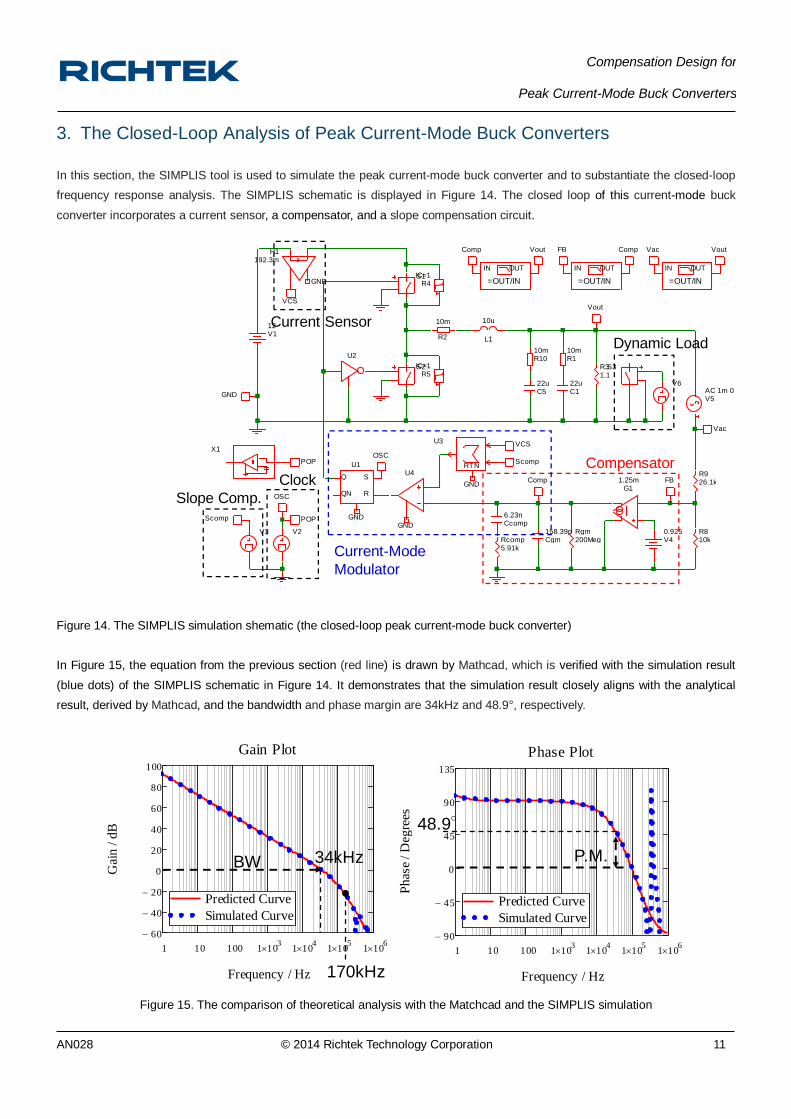
3. The Closed-Loop Analysis of Peak Current-Mode Buck Converters
In this section, the SIMPLIS tool is used to simulate the peak current-mode buck converter and to substantiate the closed-loop
frequency response analysis. The SIMPLIS schematic is displayed in Figure 14. The closed loop of this current-mode buck
converter incorporates a current sensor, a compensator, and a slope compensation circuit.
Figure 14. The SIMPLIS simulation shematic (the closed-loop peak current-mode buck converter)
In Figure 15, the equation from the previous section (red line) is drawn by Mathcad, which is verified with the simulation result
(blue dots) of the SIMPLIS schematic in Figure 14. It demonstrates that the simulation result closely aligns with the analytical
result, derived by Mathcad, and the bandwidth and phase margin are 34kHz and 48.9°, respectively.
Figure 15. The comparison of theoretical analysis with the Matchcad and the SIMPLIS simulation
1 10 100 1 103
1 104
1 105
1 106
60
40
20
0
20
40
60
80
100
Predicted Curve
Simulated Curve
Gain Plot
Frequency / Hz
Gai
n / d
B
1 10 100 1 103
1 104
1 105
1 106
90
45
0
45
90
135
Predicted Curve
Simulated Curve
Phase Plot
Frequency / Hz
Ph
ase
/ D
egre
es
BW P.M.34kHz
48.9°
170kHz
GND
VCSU3
RTNScomp
S3
=OUT/IN
OUTIN
Comp
=OUT/IN
OUTIN
VacCompFB
Comp
Scomp GNDPOP
V2
U1
Q
QN
S
R
6.23nCcomp
H1192.3m
POP
U2
10u
L1
S1
12V1
S2
10m
R2
X1
IC=1R5
IC=1R4
R926.1k
0.925V4
R810k
22uC5
10mR10
VCS
G11.25m
Rcomp5.91k
GND
OSC
OSC
GND
V3
AC 1m 0V5
=OUT/IN
OUTIN
Vout
Rgm200Meg
158.39pCgm
R31.1
Vac
Vout Vout
10mR1
22uC1
V6
GND
U4FB
Compensator
Current-Mode
Modulator
Dynamic Load
Slope Comp.
Clock
Current Sensor
Compensation Design for
Peak Current-Mode Buck Converters
AN028 © 2014 Richtek Technology Corporation 12
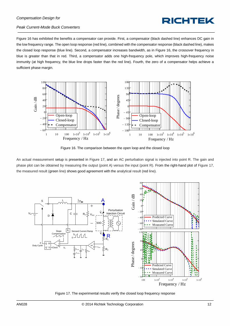
Figure 16 has exhibited the benefits a compensator can provide. First, a compensator (black dashed line) enhances DC gain in
the low frequency range. The open loop response (red line), combined with the compensator response (black dashed line), makes
the closed loop response (blue line). Second, a compensator increases bandwidth, as in Figure 16, the crossover frequency in
blue is greater than that in red. Third, a compensator adds one high-frequency pole, which improves high-frequency noise
immunity (at high frequency, the blue line drops faster than the red line). Fourth, the zero of a compensator helps achieve a
sufficient phase margin.
Figure 16. The comparison between the open loop and the closed loop
An actual measurement setup is presented in Figure 17, and an AC perturbation signal is injected into point R. The gain and
phase plot can be obtained by measuring the output (point A) versus the input (point R). From the right-hand plot of Figure 17,
the measured result (green line) shows good agreement with the analytical result (red line).
Figure 17. The experimental results verify the closed loop frequency response
1 10 100 1 103
1 104
1 105
1 106
60
40
20
0
20
40
60
80
100
Open-loop
Closed-loop
Compensator
Frequency / Hz
Gai
n /
dB
1 10 100 1 103
1 104
1 105
1 106
180
135
90
45
0
45
90
135
180
Open-loop
Closed-loop
Compensator
Frequency / Hz
Gai
n /
dB
1 10 100 1 103
1 104
1 105
1 106
60
40
20
0
20
40
60
80
100
Open-loop
Closed-loop
Compensator
Frequency / Hz
Gai
n / d
B
1 10 100 1 103
1 104
1 105
1 106
180
135
90
45
0
45
90
135
180
Open-loop
Closed-loop
Compensator
Frequency / Hz
Gai
n / d
B
1 10 100 1 103
1 104
1 105
1 106
60
40
20
0
20
Gain Plot
Frequency / Hz
Gai
n / d
B
1 10 100 1 103
1 104
1 105
1 106
225
180
135
90
45
0
45
90
135
180
225
Control-to-output
Phase Plot
Frequency / Hz
Ph
ase
/ d
egre
es
1 10 100 1 103
1 104
1 105
1 106
60
40
20
0
20
Gain Plot
Frequency / Hz
Gai
n /
dB
1 10 100 1 103
1 104
1 105
1 106
60
40
20
0
20
Gain Plot
Frequency / Hz
Gai
n /
dB
L
CD
Vin Vout
IoutS
Slope
Compensation
Ri
Vc
d
Duty Cycle
Ro
Sensed Current Ramp
Sn
0R1
R2
S
RQ
Q’ Clock
ov̂
iv̂
50Ω
Perturbation
Injection Circuit
gmVREF
Rgm
Rcomp Cgm
Ccomp
A
R1 10 100 1 10
3 1 10
4 1 10
5 1 10
6
60
40
20
0
20
Gain Plot
Frequency / Hz
Gai
n / d
B
1 10 100 1 103
1 104
1 105
1 106
60
40
20
0
20
Gain Plot
Frequency / Hz
Gai
n /
dB
1 10 100 1 103
1 104
1 105
1 106
225
180
135
90
45
0
45
90
135
180
225
Control-to-output
Phase Plot
Frequency / Hz
Ph
ase
/ d
egre
es
100 1 103
1 104
1 105
1 106
80
60
40
20
0
20
40
60
80
Predicted Curve
Simulated Curve
Measured Curve
Gain Plot
Frequency / Hz
Gai
n /
dB
100 1 103
1 104
1 105
1 106
90
45
0
45
90
135
Predicted Curve
Simulated Curve
Measured Curve
Phase Plot
Frequency / Hz
Phas
e /
Deg
rees

Compensation Design for
Peak Current-Mode Buck Converters
AN028 © 2014 Richtek Technology Corporation 13
4. Conclusion
At low frequencies, an open-loop peak current-mode buck converter is still a single-pole system since the loop control is
realized by injecting current signals into the loop only.
Its compensator is easy to design. The compensator zero is designed to cancel the dominant pole of a buck converter for
system stability.
In order to assure sufficient phase margin, the design goal is that the gain curve is at the slope -20dB / decade, when passing
the crossover frequency.
5. References
[1] V. Vorperian, “Simplified analysis of PWM converters using model of PWM switch part I:
continuous conduction mode,” IEEE Trans. on Power Electronics, vol. 26, no. 3, pp. 490-496,
May 1990.
[2] Raymond B. Ridley, A New Small-signal Model for Current-mode Control, Ph.D. Dissertation,
Virginia Polytechnic Institute and State University, Nov. 1990.
Next Steps
Richtek Newsletter Subscribe Richtek Newsletter
Richtek Technology Corporation
14F, No. 8, Tai Yuen 1st Street, Chupei City
Hsinchu, Taiwan, R.O.C.
Tel: 886-3-5526789
Richtek products are sold by description only. Richtek reserves the right to change the circuitry and/or specifications without notice at any time. Customers should obtain the latest relevant information and data sheets before placing orders and should verify that such information is current and complete. Richtek cannot assume responsibility for use of any circuitry other than circuitry entirely embodied in a Richtek product. Information furnished by Richtek is believed to be accurate and reliable. However, no responsibility is assumed by Richtek or its subsidiaries for its use; nor for any infringements of patents or other rights of third parties which may result
from its use. No license is granted by implication or otherwise under any patent or patent rights of Richtek or its subsidiaries.