cmos temperature sensors using peaking current source - …especially those of transistor and...
TRANSCRIPT
Buletinul Ştiinţific al Universităţii "Politehnica" din Timişoara
Seria ELECTRONICĂ şi TELECOMUNICAŢII TRANSACTIONS on ELECTRONICS and COMMUNICATIONS
Tom 56 (70), Fascicola 1, 2011
CMOS Temperature Sensors Using Peaking Current Source
Bogdan V. Marinca1, Mircea A. Ciugudean
1 Facultatea de Electronică şi Telecomunicaţii, Departamentul Electronică Aplicată, Bd. V. Pârvan Nr. 2, 300223 Timişoara, e-mail: [email protected]
Abstract – Two new CMOS analog temperature sensors, obtained from known reference voltage sources, are presented. They are realized by two cross-connected current mirrors, one of which being a peaking source. The temperature sensor behaviour was obtained here by corresponding design, made with the goal to achieve a maximum output-voltage slope. The two circuits were conceived in 0.35µm CMOS process and realize some superior performances in comparison with known analog temperature sensors: slope of order 1.5mV/oC, minimum supply voltage of 1.5V, small supply current, very good SR and PSRR parameters, small area on chip. The output-voltage total process variation is 2%. Keywords: temperature sensors, CMOS analog sensors, process variation
I. INTRODUCTION
The performing smart temperature sensors are more and more used in VLSI modern systems. One may find from the publications the temperature sensors in CMOS chips constitute an important academic and industrial research subject of last 20 years. The actuality of the research in the domain of smart temperature sensors is proved by the great number of published papers, books and PhD theses. In [2] a great number of applications, requiring the temperature sensor use, were gathered up. The domain stage of the analog temperature sensors, representing the front-end part of the smart sensors, is commented. Were presented the numerous conditions imposed to integrated temperature sensors. Based on bibliographic study (over 50 papers, books and PhD theses) one achieved, on much criteria, a more complete classification than the encountered in publications one. There too, were presented comparatively and were commented the known or estimated by the author performances of the proper (front-end) analog sensors, separately from the smart sensors. The table which presents the comparative performances of known sensors shows the fact that neither sensor fulfils simultaneously all the imposed requirements, especially that of scheme complexity and the output voltage or current process variation. This means the researches aiming sensor improvement must be continued.
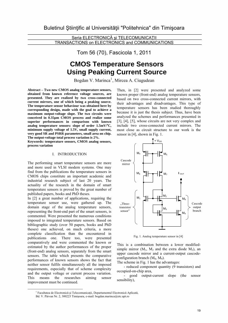
Then, in [2] were presented and analyzed some known proper (front-end) analog temperature sensors, based on two cross-connected current mirrors, with their advantages and disadvantages. This type of temperature sensors has been studied thoroughly because it is just the thesis subject. Thus, have been analyzed the schemes and performances presented in [3], [4], [5], whose circuits are not very complex and include two cross-connected current mirrors. The most close as circuit structure to our work is the sensor in [4], shown in Fig. 1.
This is a combination between a lower modified-simple mirror (M1, M2 and the extra diode M3), an upper cascode mirror and a current-output cascode-configuration branch (M8, M9). The scheme in Fig. 1 has the advantages: - reduced component quantity (9 transistors) and occupied-on-chip area, - good output-current slope (the sensor sensibility),
Fig. 1. Analog temperature sensor in [4]
„Three-transistor sensor”
Cascode output branch
IOUT
M5
+VDD
M4
M1
M3
M2
M7
M9
Cascode mirror
M8
M6
19
- good isolation of the output against supply-voltage perturbations (thanks to cascodes). The scheme disadvantages are: - high supply-voltage minimum value, 5V (for CMOS-1µm process, which may be scaled), - high nonlinearity of current-temperature characteristic, - lack of process-variation-effect (on the output current) verification, which may be important because of VT-voltage dependence on process parameters. Another above-cited two schemes, [3], [5], include more complex circuits (15 transistors and 3 bias-voltage sources respectively 10 transistors and 3 bias-voltage sources). Table 1 presents comparatively the performances of above-cited three analog temperature sensors. Some of sensor’s data do not exist in the respective papers. One may see the sensor sensibility is modest or even poor, and sensible smaller as another-principle schemes or those proposed by us ourselves in [2]. Then, some of these schemes have higher complexity and nonlinearity. Some performances are obtained by cascode configurations. It may be observed, one not yet disposes of an analog
circuit which fulfils all the requirements imposed to front-end temperature sensors in the smart sensors. None of these schemes use the Wilson-peaking or Widlar-peaking configuration, proposed in this work. Our sensor schemes or another close to this, have not been encountered in literature with the destination of temperature sensor but with that of current or voltage references [1], [6], [7]. The basic idea to achieving the two sensors started from known identical reference voltage source schemes [1] which were designed here so the output voltage has a strong temperature linear dependency and maximum slope. The proposed circuits consist of two classical cross-connected mirrors, where the lower mirror is a Wilson or modified-Widlar one [1] (with an extra diode on the left branch) and the upper one is a peaking mirror. The schematic uses integrated resistors whose I-order temperature coefficient is of particular type. Section II presents the proposed Wilson-peaking temperature sensor and his performances. Section III presents the proposed Widlar-peaking one and his performances. Section IV presents the conclusions of this paper.
Table 1. Some proper-analog (front-end)-temperature-sensor performances Ref. CMOS
process
Component number
Chip area
Sensibility (slope)
Temperature range
Nonlinearity
Process variation
VDDmin / Supply current
[µm] µm2 °C % % V / µA
[3] 0.8 27 0.7 mV/°C -43...127 0.12 1,6 / 0,03 [4] 1 9 2800 0.08 µA/°C 10...100 ±1.5 5 / 20 [5] 0.18 >20 1320 5.6 nA/°C 0...80 1.3 4 1,8 / 25
II. THE WILSON-PEAKING SENSOR The circuit, shown in Fig.2, achieved by a cross-connection of a lower modified-Wilson current mirror (M1, M2 and R1) and an upper peaking mirror (M3, M4 and R2), is known as voltage reference [1] but, in our work, it is converted by design in a temperature sensor [2]. The output is considered not charged but the load (resistor) may be included in parallel with R1. The output-voltage thermal-sensibility calculus and sensibility optimisation may be done in a same procedural manner as that presented in [2] but it is extremely complex because the transistors M1 and M4 work in weak-inversion regime. The simulation of the Wilson-peaking sensor of Fig.2 has been done in the temperature range of -30...120ºC. To find the output-voltage maximum slope one achieved a great quantity of simulations, for different values of: R1 and R2 resistors and resistance temperature coefficients (type NTC and PTC resistors). The best results were obtained for: R1=80kΩ, R4=2.7kΩ, both of NTC type, and transistor dimensions: L1,2,3,4=5µm, W1=85µm, W2=5µm, W3=0,5µm and W4=80µm. Comparatively with known schemes, analysed in [2], this type of sensor presents some good performances:
+VDD I2
M3 M4
M1
M2
R1
I1
VOUT
R2
Fig. 2. Wilson-peaking temperature-sensor scheme
20
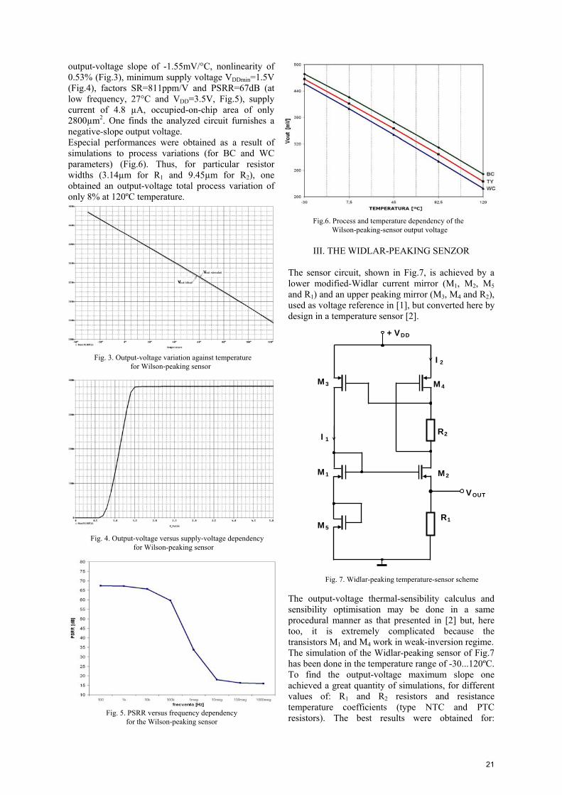
output-voltage slope of -1.55mV/°C, nonlinearity of 0.53% (Fig.3), minimum supply voltage VDDmin=1.5V (Fig.4), factors SR=811ppm/V and PSRR=67dB (at low frequency, 27°C and VDD=3.5V, Fig.5), supply current of 4.8 µA, occupied-on-chip area of only 2800µm2. One finds the analyzed circuit furnishes a negative-slope output voltage. Especial performances were obtained as a result of simulations to process variations (for BC and WC parameters) (Fig.6). Thus, for particular resistor widths (3.14µm for R1 and 9.45µm for R2), one obtained an output-voltage total process variation of only 8% at 120ºC temperature.
Fig.6. Process and temperature dependency of the
III. THE WIDLAR-PEAKING SENZOR The sensor circuit, shown in Fig.7, is achieved by a lower modified-Widlar current mirror (M1, M2, M5 and R1) and an upper peaking mirror (M3, M4 and R2), used as voltage reference in [1], but converted here by design in a temperature sensor [2].
Wilson-peaking-sensor output voltage
Fig. 7. Widlar-peaking temperature-sensor scheme
+VDD
The output-voltage thermal-sensibility calculus and sensibility optimisation may be done in a same procedural manner as that presented in [2] but, here too, it is extremely complicated because the transistors M1 and M4 work in weak-inversion regime. The simulation of the Widlar-peaking sensor of Fig.7 has been done in the temperature range of -30...120ºC. To find the output-voltage maximum slope one achieved a great quantity of simulations, for different values of: R1 and R2 resistors and resistance temperature coefficients (type NTC and PTC resistors). The best results were obtained for:
Fig. 3. Output-voltage variation against temperature I2 for Wilson-peaking sensor M3 M4
I1 R2
M1 M2
R1 M5
VOUT
Fig. 5. PSRR versus frequency dependency
Fig. 4. Output-voltage versus supply-voltage dependency for Wilson-peaking sensor
for the Wilson-peaking sensor
21
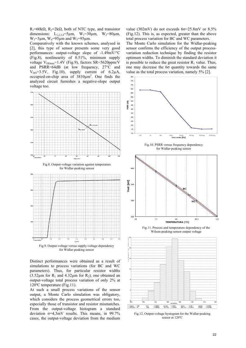
R1=60kΩ, R2=2kΩ, both of NTC type, and transistor dimensions: L1,2,3,4=5µm, W1=30µm, W2=80µm, W3=3µm, W4=95µm and W5=95µm. Comparatively with the known schemes, analysed in [2], this type of sensor presents some very good performances: output-voltage slope of -1.49mV/°C (Fig.8), nonlinearity of 0.51%, minimum supply voltage VDDmin=1.4V (Fig.9), factors SR=5620ppm/V and PSRR=64dB (at low frequency, 27°C and VDD=3.5V, Fig.10), supply current of 6.2µA, occupied-on-chip area of 3810µm2. One finds the analyzed circuit furnishes a negative-slope output voltage too. Distinct performances were obtained as a result of simulations to process variations (for BC and WC parameters). Thus, for particular resistor widths (3.52µm for R1 and 4.32µm for R2), one obtained an output-voltage total process variation of only 2% at 120ºC temperature (Fig.11). At such a small process variations of the sensor output, a Monte Carlo simulation was obligatory, which considers the process geometrical errors too, especially those of transistor and resistor mismatches. From the output-voltage histogram a standard deviation σ=4,3mV results. This means, in 99.7% cases, the output-voltage deviation from the medium
value (302mV) do not exceeds 6σ=25.8mV or 8.5% (Fig.12). This is, as expected, greater than the above total process variation for BC and WC parameters. The Monte Carlo simulation for the Widlar-peaking sensor confirms the efficiency of the output process-variation reduction technique by finding the resistor optimum widths. To diminish the standard deviation it is possible to reduce the great resistor R1 value. Thus, one may decrease the 6σ quantity towards the same value as the total process variation, namely 5% [2]. Fig.10. PSRR versus frequency dependency
for Widlar-peaking sensor
Fig.8. Output-voltage variation against temperature for Widlar-peaking sensor
Fig.11. Process and temperature dependency of the Wilson-peaking-sensor output voltage
Fig.9. Output-voltage versus supply-voltage dependency for Widlar-peaking sensor
Fig.12. Output-voltage hystogram for the Widlar-peaking
sensor at 120oC
22
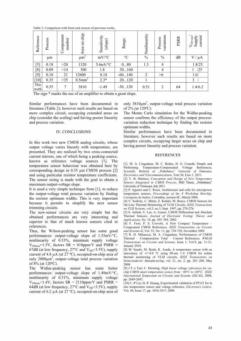
Table 2. Comparison with front-end sensors of previous works.
Ref
eren
ce
Proc
ess
Com
pone
nt
num
ber
Are
a on
chi
p
Sens
itivi
ty
(slo
pe)
Ran
ge
Non
linea
rity
Proc
ess
varia
tions
PSR
R
VD
D m
in/
Supp
ly
curr
ent
µm µm2 mV/°C °C % % dB V / µA
[5] 0.18 >20 1320 5.6nA/°C 0...80 1.3 4 1.8/25 [8] 0.09 >14 300 1.8 30...160 4 1 /25 [9] 0.18 21 12600 0.18 -60...140 2 >6 1.6/
[10] 0.35 >35 0.5mm2 2.3* 20...120 1 3 / This work 0.35 7 3810 -1.49 -30...120 0.51 2 64 1.4/6.2
The sign * marks the use of an amplifier to obtain a great slope. Similar performances have been documented in literature (Table 2); however such results are based on more complex circuit, occupying extended areas on chip (consider the scaling) and having poorer linearity and process variation.
IV. CONCLUSIONS In this work two new CMOS analog circuits, whose output voltage varies linearly with temperature, are presented. They are realized by two cross-connected current mirrors, one of which being a peaking source, known as reference voltage sources [1]. The temperature sensor behaviour was obtained here by corresponding design in 0.35 µm CMOS process [2] and using particular resistor temperature coefficients. The sensor sizing is made with the goal to obtain a maximum output-voltage slope. It is used a very simple technique from [1], to reduce the output-voltage total process variation by finding the resistor optimum widths. This is very important because it permits to simplify the next sensor trimming circuits. The new-sensor circuits are very simple but the obtained performances are very interesting and superior to that of much known sensors cited in references. Thus, the Wilson-peaking sensor has some good performances: output-voltage slope of 1.55mV/°C, nonlinearity of 0.53%, minimum supply voltage VDDmin=1.5V, factors SR = 810ppm/V and PSRR = 67dB (at low frequency, 27°C and VDD=3.5V), supply current of 4.8 µA (at 27 ºC), occupied-on-chip area of only 2800µm2, output-voltage total process variation of 8% (at 120ºC). The Widlar-peaking sensor has some better performances: output-voltage slope of 1.49mV/°C, nonlinearity of 0.51%, minimum supply voltage VDDmin=1.4V, factors SR = 2110ppm/V and PSRR = 64dB (at low frequency, 27°C and VDD=3.5V), supply current of 6.2 µA (at 27 ºC), occupied-on-chip area of
only 3810µm2, output-voltage total process variation of 2% (at 120ºC). The Monte Carlo simulation for the Widlar-peaking sensor confirms the efficiency of the output process-variation reduction technique by finding the resistor optimum widths. Similar performances have been documented in literature; however such results are based on more complex circuits, occupying larger areas on chip and having poorer linearity and process variation.
REFERENCES
[1]. M. A. Ciugudean, M. C. Bodea, H. G. Coandă, Simple and Performing Temperature-Compensated Voltage References, Scientific Bulletin of „Politehnica” University of Timisoara, Electronics and Telecommunications, Tom 56, Fasc.1, 2011. [2] V. B. Marinca, Conception and Design of New Temperature Sensors Integrated in CMOS Process, PhD Thesis, „Politehnica” University of Timisoara, July 2011. [3] P. Aguirre and C. Rossi, Architecture and cells for micropower temperature sensors, Proceedings of the X Workshop Iberchip, Cartagena de Indias, Colombia, session 6C, March 2004. [4] V. Székely, C. Márta, Z. Kohári, M. Rencz, CMOS Sensors for On-Line Thermal Monitoring of VLSI Circuits, IEEE Transactions on VLSI Systems, vol.5, no.3, Sept. 1997, pp. 270-276. [5] S. Ashish, V. Lee, A. Ivanov, CMOS Differential and Absolute Thermal Sensors, Journal of Electronic Testing: Theory and Applications, No. 18, pp. 295–304, 2002. [6] F. Fiori, P. S. Crovetti, A New Compact Temperature – Compesated CMOS References, IEEE Transactions on Circuits and Systems-II, Vol. 52, No. 11, pp. 724-728, November 2005. [7] R. D. Mihaescu, M. A. Ciugudean, Performances of CMOS Thermal – Compensation Total – Current References, WSEAS Transactions on Circuits and Systems, Issue 1, Vol.9, pp. 11-21, January 2010. [8] M. Sasaki, M. Ikeda, K. Asada, A temperature sensor with an inaccuracy of -1/+0.8 ºC using 90-nm 1-V CMOS for online thermal monitoring of VLSI circuits, IEEE Transactions on Semiconductor Manufacturing, vol. 21, no. 2, pp. 201–208, May 2008. [9] J.T.-s Tsai, C. Herming, High linear voltage references for on-chip CMOS smart temperature sensor from −60°C to 140°C, IEEE International Symposium on Circuits and Systems (ISCAS), 2008, pp. 2689-2692. [10] C.-P Liu, H.-P. Huang, Experimental validation of PTAT for in situ temperature sensor and voltage reference, Electronics Letters, Vol. 44, Issue 17, pp. 1016-1017, 2008.
23