cmos analog design lecture notes rev 1hoppe.eit.h-da.de/msc/cmos analog design lecture... · prof....
TRANSCRIPT
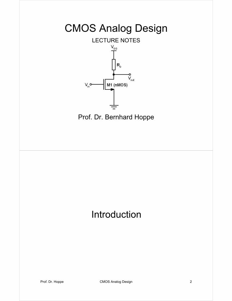
CMOS Analog DesignLECTURE NOTES
Prof. Dr. Bernhard Hoppe
Prof. Dr. Hoppe CMOS Analog Design 2
Introduction
Prof. Dr. Hoppe CMOS Analog Design 3
Analog Integrated Circuits Design Steps:
1. Definition
2. Implementation
3. Simulation
4. Geometrical description
5. Simulation including the geometrical parasitics
6. Fabrication
7. Testing and verification
Prof. Dr. Hoppe CMOS Analog Design 4
Analog Integrated Circuits Design:
Tools & Methods:
• Simulation
• Design Capture
• Hand Calculations
Bottom – Up Flow
Prof. Dr. Hoppe CMOS Analog Design 5
Discrete Analog Circuit Design
- Using breadboards
Integrated Analog Circuit Design
- Using computer simulation techniques
Prof. Dr. Hoppe CMOS Analog Design 6
Pros and Cons of Computer simulations
Advantages:
1. No breadboards required
2. Every node in the circuit is accessible
3. Feedback loops may be opened
4. Modification of the circuit is easy
5. Modification of processes and ambient conditions is possible

Prof. Dr. Hoppe CMOS Analog Design 7
Pros and Cons of Computer simulations
Drawbacks:
1. Accuracy of models
2. Convergence problems of the simulator: circuit may not converge to a stable operating point
3. Time required to perform simulations of large circuits
4. Use of the computer as a substitute for thinking
Prof. Dr. Hoppe CMOS Analog Design 8
The PN junction
Prof. Dr. Hoppe CMOS Analog Design 9
PN junction
Used for:
1. Insulation purposes
2. Diodes and zeners
3. Basic structure of MOS and Bipolar transistor
Prof. Dr. Hoppe CMOS Analog Design 10
Important features for device properties
And modelling aspects
• Depletion region width
• Depletion region capacitance
• Reverse bias breakdown voltage
• Diode equation iD Vs VD
Prof. Dr. Hoppe CMOS Analog Design 11
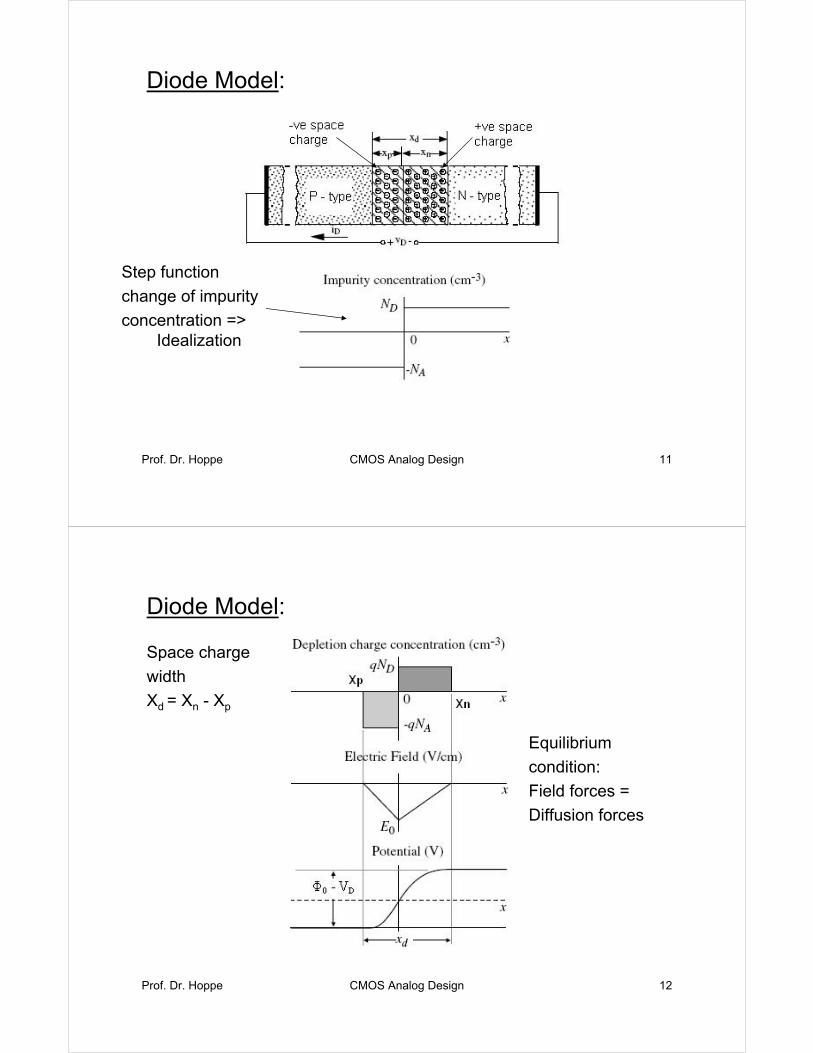
Diode Model:
Step function
change of impurity
concentration => Idealization
Prof. Dr. Hoppe CMOS Analog Design 12
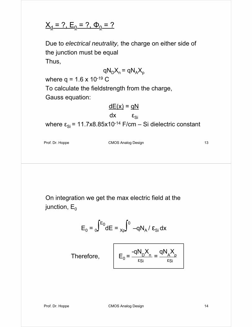
Diode Model:
Space charge
width
Xd = Xn - Xp
Equilibrium
condition:
Field forces =
Diffusion forces
Prof. Dr. Hoppe CMOS Analog Design 13
Xd = ?, E0 = ?, Φ0 = ?
Due to electrical neutrality, the charge on either side of
the junction must be equal
Thus,
qNDXn = qNAXp
where q = 1.6 x 10⁻¹⁹ C
To calculate the fieldstrength from the charge,
Gauss equation:
dE(x) = qN
dx εSi
where εSi = 11.7x8.85x10-14 F/cm – Si dielectric constant
Prof. Dr. Hoppe CMOS Analog Design 14
On integration we get the max electric field at the
junction, E0
E0 = 0∫E0
dE = Xp∫0
–qNA / εSi dx
Therefore, E0 = -qN
DX
n = qN
AX
p εSi εSi
Prof. Dr. Hoppe CMOS Analog Design 15
Voltage is found by integrating the electric field, resulting
in
Φ0 - VD = -E
0(X
n – X
p)
2
where VD = applied external voltage
Φ0 = barrier potential
Prof. Dr. Hoppe CMOS Analog Design 16
Barrier potential Φ0 is given as
Φ0 = (kT / q) ln (NAND / ni2) = (Vt) ln (NAND / ni
2)
where k = Boltzmann‘s constant 1.38 x 10⁻²³ J/K
ni = intrinsic concentration of silicon
1.45 x 10¹⁰ /cm3 at 300K
Vt = 25.9 mV at 300K
Prof. Dr. Hoppe CMOS Analog Design 17
Using equations for E0 and Φ0 – VD, and solving for Xn
or Xp we get
Xn = ( 2εSi(Φ0 – VD)NA )1/2
qND(N
A + N
D)
and Xp = - ( 2εSi(Φ0 – VD)ND )1/2
qNA(N
A + N
D)
Prof. Dr. Hoppe CMOS Analog Design 18
Width of the depletion region Xd is given as
Xd = Xn – Xp = ( 2εSi(NA + ND) )1/2
(Φ0 - VD)1/2
qNAN
D
Prof. Dr. Hoppe CMOS Analog Design 19
Conclusions:
1. Xd is proportional to (Φ0 - VD)1/2 or (- VD)1/2
2. If NA >> ND then Xd ~ Xn
3. If ND >> NA then Xd ~ Xp
4. Lower doped side determines Xd
Prof. Dr. Hoppe CMOS Analog Design 20
Depletion charge and depletion layer
capacitance:Depletion charge Qj is given as
Qj = |AqNAXp| = AqNDXn
Qj = A( 2εSiqNAND )1/2
(Φ0 - VD)1/2
(NA+N
D)
where A is the cross sectional area of the pn junction
Prof. Dr. Hoppe CMOS Analog Design 21
Depletion charge and depletion layer
capacitance:Magnitude of the electric field at the junction
E0 = ( 2qNAND )1/2(Φ0 - VD)1/2
εSi(N
A+N
D)
Prof. Dr. Hoppe CMOS Analog Design 22
Depletion charge and depletion layer
capacitance:Depletion layer capacitance Cj is given as
Cj = dQj
= A( εSiqNAND )1/2(Φ0 - VD)-1/2
dVD 2(NA+ND)
=Cj0
[1-(VD /Φ0)]m
Prof. Dr. Hoppe CMOS Analog Design 23
Depletion charge and depletion layer
capacitance:where Cj0 is capacitance when VD = 0
m is a grading coefficient
m = 1/2 => step junction
m = 1/3 => linearly graded junction
1/3 <= m <= 1/2 => real junctions
(experimental fit)
Prof. Dr. Hoppe CMOS Analog Design 24
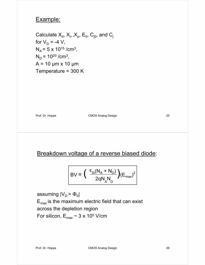
Plot of the space charge capacitance:
Ideal
Actual
Prof. Dr. Hoppe CMOS Analog Design 25
Example:
Calculate Xd, Xn ,Xp, E0, Cj0, and Cj
for VD = -4 V,
NA = 5 x 10¹⁵ /cm3,
ND = 1020 /cm3,
A = 10 µm x 10 µm
Temperature = 300 K
Prof. Dr. Hoppe CMOS Analog Design 26
Breakdown voltage of a reverse biased diode:
BV = ( εSi(NA + ND) )(Emax)2
2qNAN
D
assuming |VD > Φ0|
Emax is the maximum electric field that can exist
across the depletion region
For silicon, Emax ~ 3 x 10⁵ V/cm
Prof. Dr. Hoppe CMOS Analog Design 27
Breakdown mechanisms:
1. Avalanche breakdown: Multiplication of carrier concentrations due to collisions of minority carriers with the lattice electrons. It has a negative temperature coefficient.
2. Zener breakdown: Valence band breakdown. It occurs at comparatively lower voltages. It does not depend upon temperature (tunneling effect).
Prof. Dr. Hoppe CMOS Analog Design 28
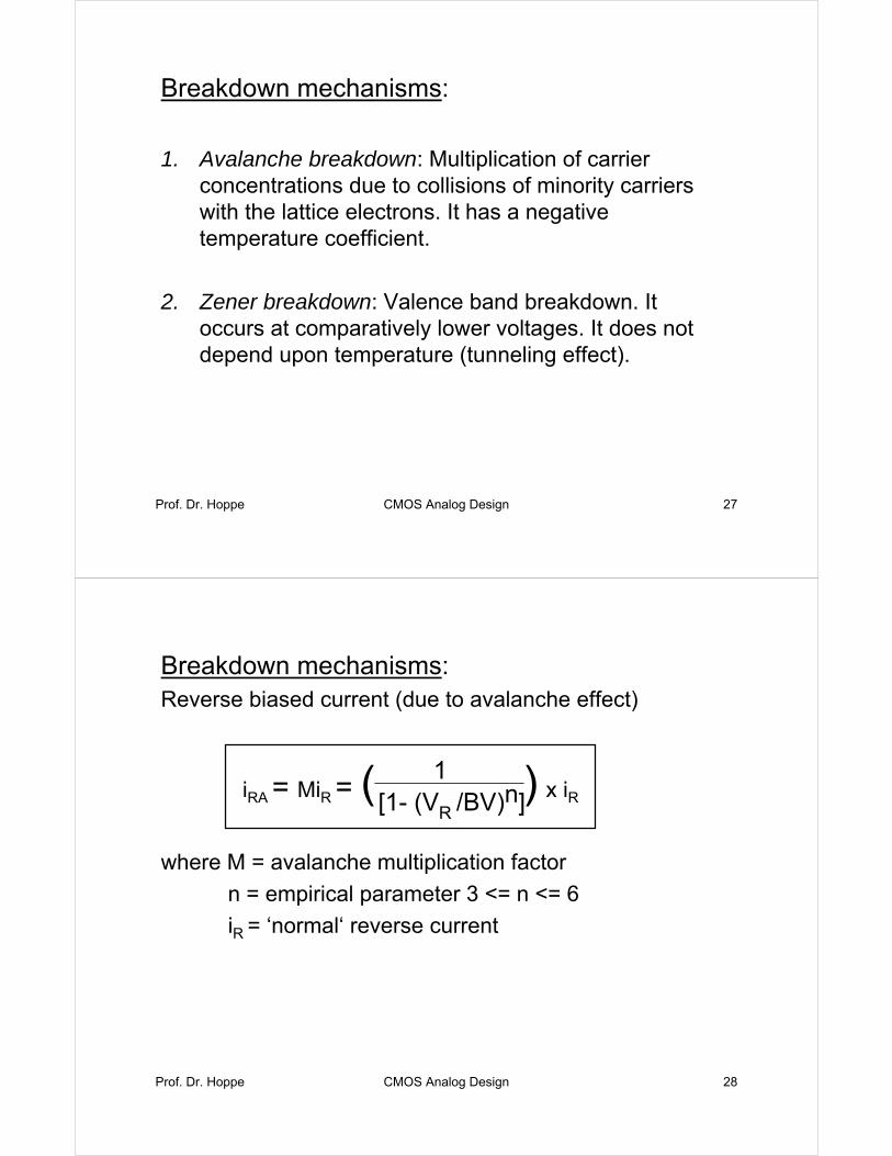
Breakdown mechanisms: Reverse biased current (due to avalanche effect)
iRA = MiR = ( 1 ) x iR[1- (VR /BV)n]
where M = avalanche multiplication factor
n = empirical parameter 3 <= n <= 6
iR = ‘normal‘ reverse current
Prof. Dr. Hoppe CMOS Analog Design 29
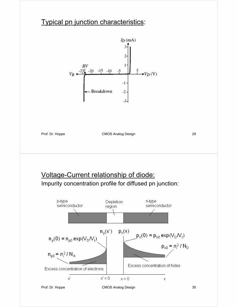
Typical pn junction characteristics:
Prof. Dr. Hoppe CMOS Analog Design 30
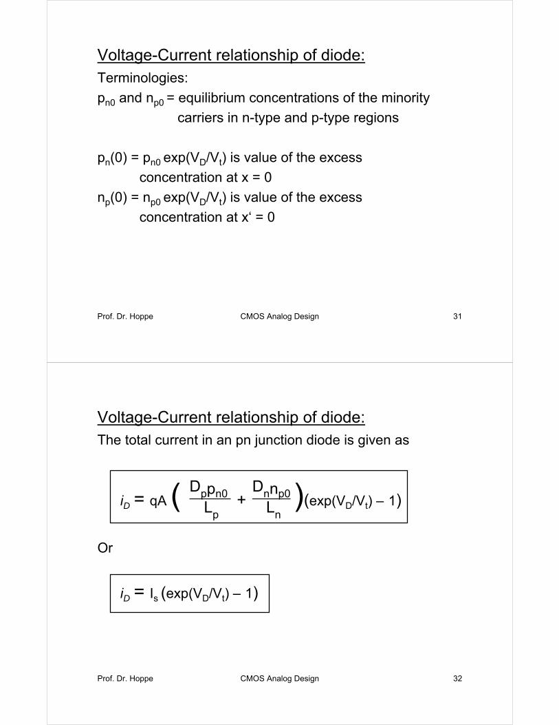
Voltage-Current relationship of diode:Impurity concentration profile for diffused pn junction:
Prof. Dr. Hoppe CMOS Analog Design 31
Voltage-Current relationship of diode:Terminologies:
pn0 and np0 = equilibrium concentrations of the minority
carriers in n-type and p-type regions
pn(0) = pn0 exp(VD/Vt) is value of the excess
concentration at x = 0
np(0) = np0 exp(VD/Vt) is value of the excess
concentration at x‘ = 0
Prof. Dr. Hoppe CMOS Analog Design 32
Voltage-Current relationship of diode:The total current in an pn junction diode is given as
iD = qA ( Dppn0 +Dnnp0 )(exp(VD/Vt) – 1)Lp Ln
Or
iD = Is (exp(VD/Vt) – 1)
Prof. Dr. Hoppe CMOS Analog Design 33
Voltage-Current relationship of diode:where
Is = qA ( Dppn0 +Dnnp0 )Lp Ln
is a constant called the saturation currentA = area of the pn junctionDp = diffusion constant of holes in n-type semiconductorDn = diffusion constant of electrons in p-type
semiconductorLp = diffusion length for holes in n-type semiconductorLp = diffusion length for el in p-type semiconductor
Prof. Dr. Hoppe CMOS Analog Design 34
Example:
Calculate the saturation current of a pn junction diode
with
NA = 5 x 10¹⁵ /cm3, ND = 1020 /cm3,
A = 1000 µm2 , Dn = 20 cm2 / s,
Dp = 10 cm2 / s, Ln = 10 µm,
Lp = 5 µm.
Prof. Dr. Hoppe CMOS Analog Design 35
The MOS transistor
Prof. Dr. Hoppe CMOS Analog Design 36
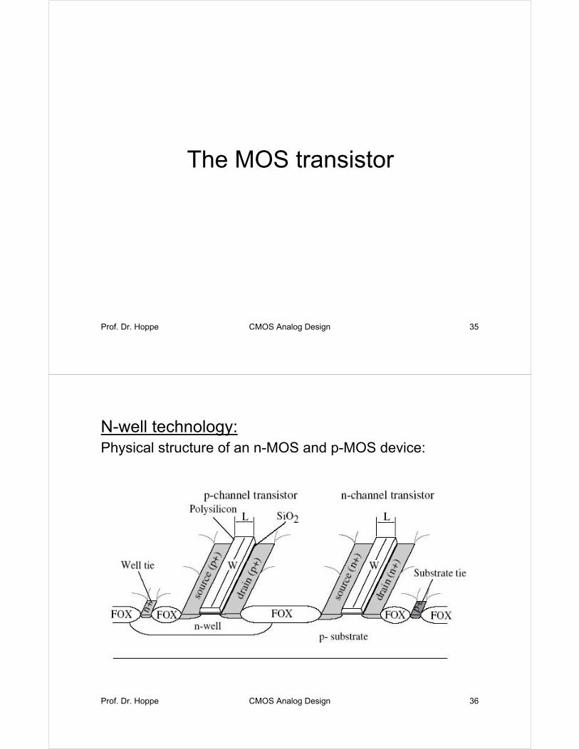
N-well technology:Physical structure of an n-MOS and p-MOS device:
Prof. Dr. Hoppe CMOS Analog Design 37
N-well technology:
• pMOS formed within a lightly doped n- material called the N-well
• nMOS formed within a lightly doped p- substrate• Both types of transistors are four terminal devices• The p-bulk connection is common throughout the
integrated circuit and is connected to Vss (the most negative supply)
• Multiple n-wells can be connected to different potentials (but +ve w.r.t. Vss)
• nMOS and pMOS devices are complementary: nMOS equations can be mapped to pMOS equations
Prof. Dr. Hoppe CMOS Analog Design 38
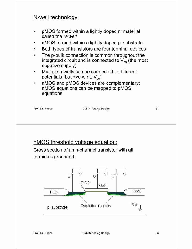
nMOS threshold voltage equation:Cross section of an n-channel transistor with all
terminals grounded:
Prof. Dr. Hoppe CMOS Analog Design 39
nMOS threshold voltage equation:Terminologies:
Cox = Area specific oxide capacitance in F/m2
ΦF = Equilibrium electrostatic potential (Fermi potential) in
the semiconductor
ΦS = Surface potential of the semiconductor
ΦMS = Difference in the work functions between the gate
material and bulk silicon in the channel region
QSS = Undesired +ve charge present in the interface
between the oxide and the bulk silicon
Qb0 = Fixed charge in the depletion region
VSB = Substrate bias (VSource - VSubstrate)
Prof. Dr. Hoppe CMOS Analog Design 40
nMOS threshold voltage equation:Threshold voltage VT consists of following contributions:
1. ΦMS = ΦF (substrate) - ΦF (gate)
where ΦF (metal) = 0.6 V
2. [-2ΦF – (Qb /Cox)]: voltage required to change the surface potential and offset the depletion layer charge
3. Undesired +ve charge QSS due to impurities and imperfections at the interface – must be compensated by a gate voltage of – QSS /Cox
Prof. Dr. Hoppe CMOS Analog Design 41
nMOS threshold voltage equation:Summation of the contributions:
VT = ΦMS + [-2ΦF – (Qb /Cox )] + (– QSS /Cox )
= ΦMS - 2ΦF – (Qb0 /Cox ) – (QSS /Cox ) - (Qb - Qb0 ) / Cox
The threshold voltage can be rewritten as
VT = VT0 + γ [√ |-2ΦF + VSB| - √ |-2ΦF| ]
where VT0 = ΦMS - 2ΦF – (Qb0 /Cox ) – (QSS /Cox )
Prof. Dr. Hoppe CMOS Analog Design 42
Body effect coefficient:The body factor, body effect coefficient, or bulk-threshold
parameter γ is defined as
γ = √2qεSiNA
(unit: V1/2)Cox
Prof. Dr. Hoppe CMOS Analog Design 43
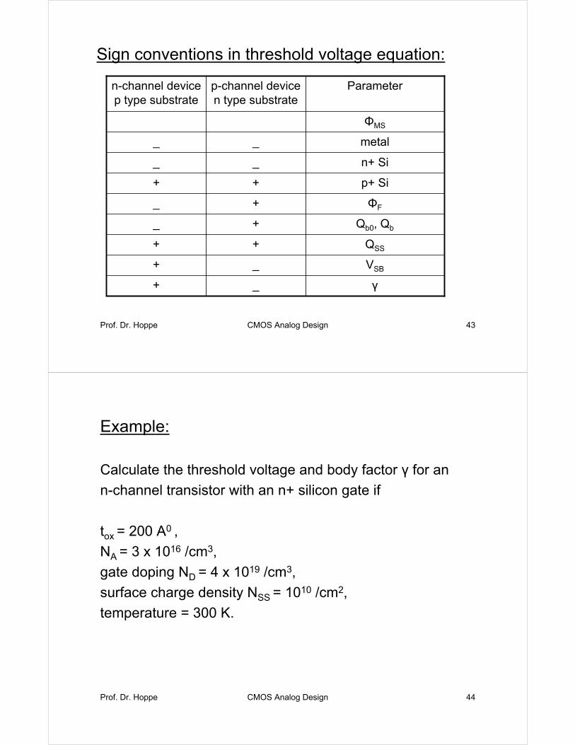
Sign conventions in threshold voltage equation:
VSB_+
n+ Si__
γ_+
QSS++
Qb0, Qb+_
ΦF+_
p+ Si++
metal__
ΦMS
Parameterp-channel device n type substrate
n-channel device p type substrate
Prof. Dr. Hoppe CMOS Analog Design 44
Example:
Calculate the threshold voltage and body factor γ for an
n-channel transistor with an n+ silicon gate if
tox = 200 A0 ,
NA = 3 x 10¹⁶ /cm3,
gate doping ND = 4 x 10¹⁹ /cm3,
surface charge density NSS = 1010 /cm2,
temperature = 300 K.
Prof. Dr. Hoppe CMOS Analog Design 45
Current voltage relation of the MOS transistor:1. Linear mode: - Sah equation
iD = (W/L)µnCox [(VGS – VT) – (VDS/2)] VDS
holds good for (VGS – VT) >= VDS and VGS >= VT
2. Saturation mode:
iD = (W/2L)µnCox [(VGS – VT)2]
holds good for (VGS – VT) <= VDS
Prof. Dr. Hoppe CMOS Analog Design 46
Device transconductance parameter:
The factor µnCox is defined as the device
transconductance parameter, given as
K‘ = µnCox = µnεox / tox
Prof. Dr. Hoppe CMOS Analog Design 47
CMOS device modeling
Prof. Dr. Hoppe CMOS Analog Design 48
Pinch-off Saturation:
• Voltage drop in the channel is constant
• The Field pulling the electrons from the source remains constant
• iD remains constant
• Electrons are injected from the channel into the space charge region => ballistic transport to drain node
Prof. Dr. Hoppe CMOS Analog Design 49
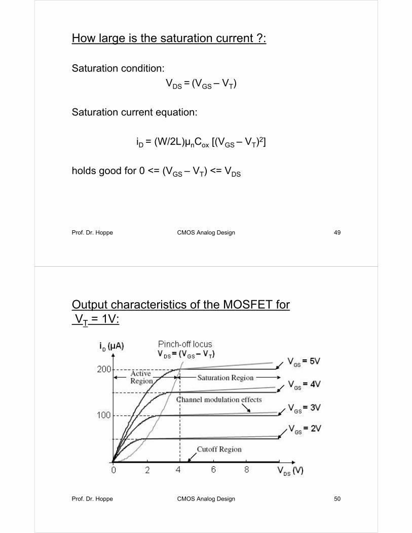
How large is the saturation current ?:
Saturation condition:
VDS = (VGS – VT)
Saturation current equation:
iD = (W/2L)µnCox [(VGS – VT)2]
holds good for 0 <= (VGS – VT) <= VDS
Prof. Dr. Hoppe CMOS Analog Design 50
Output characteristics of the MOSFET forVT = 1V:
Prof. Dr. Hoppe CMOS Analog Design 51
Channel length modulation effect:
• Constant saturation current – only for long channeldevices i.e. Pinch-off point „close“ to the drain
• Long channel devices have length L >= 10 µm
• For lengths shorter than 1 µm, short channel effects are observed
• Most important effect: Channel length modulation effect
Prof. Dr. Hoppe CMOS Analog Design 52
Channel length modulation effect:
• In reality, the saturation current depends linearly on VDS
• Modified current equation:
iD = (W/2L) µnCox [(VGS – VT)2 (1 + λVDS)]
where λ = channel length modulation factor (unit: 1/V)
Prof. Dr. Hoppe CMOS Analog Design 53
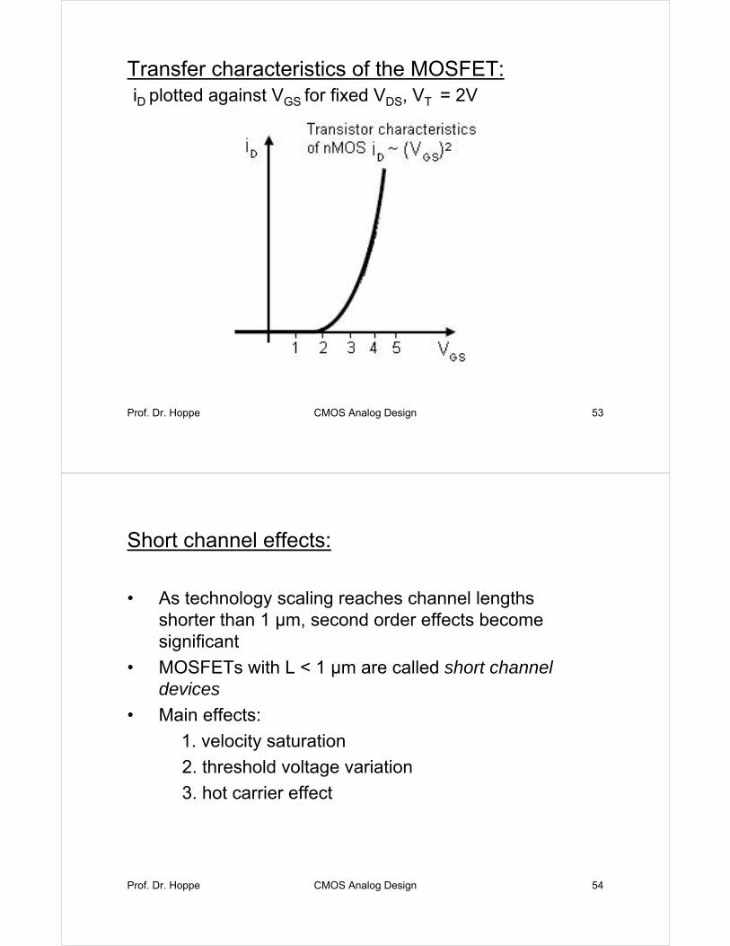
Transfer characteristics of the MOSFET:iD plotted against VGS for fixed VDS, VT = 2V
Prof. Dr. Hoppe CMOS Analog Design 54
Short channel effects:
• As technology scaling reaches channel lengths shorter than 1 µm, second order effects become significant
• MOSFETs with L < 1 µm are called short channel devices
• Main effects:
1. velocity saturation
2. threshold voltage variation
3. hot carrier effect
Prof. Dr. Hoppe CMOS Analog Design 55
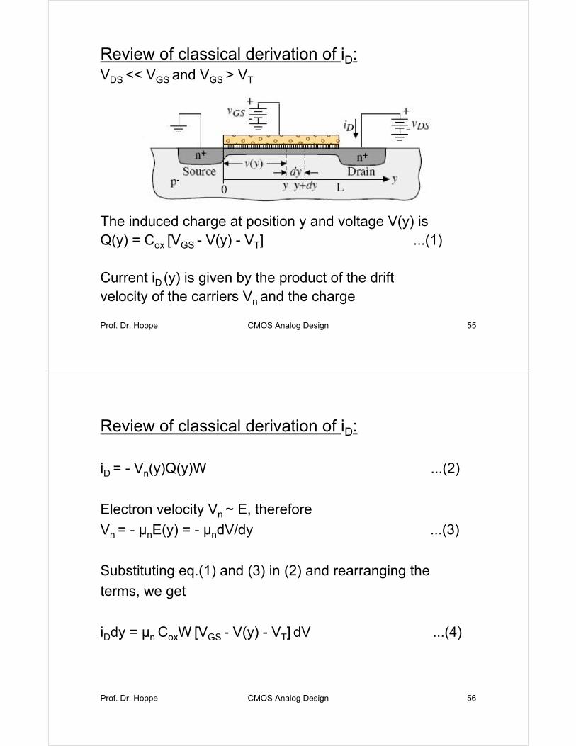
Review of classical derivation of iD:VDS << VGS and VGS > VT
The induced charge at position y and voltage V(y) isQ(y) = Cox [VGS - V(y) - VT] ...(1)
Current iD (y) is given by the product of the drift velocity of the carriers Vn and the charge
Prof. Dr. Hoppe CMOS Analog Design 56
Review of classical derivation of iD:
iD = - Vn(y)Q(y)W ...(2)
Electron velocity Vn ~ E, therefore
Vn = - µnE(y) = - µndV/dy ...(3)
Substituting eq.(1) and (3) in (2) and rearranging the
terms, we get
iDdy = µn CoxW [VGS - V(y) - VT] dV ...(4)
Prof. Dr. Hoppe CMOS Analog Design 57
Review of classical derivation of iD:
Integrating eq.(4) along the channel for 0 to L gives
iD = (W/L)µnCox [(VGS – VT) – (VDS/2)] VDS
Prof. Dr. Hoppe CMOS Analog Design 58
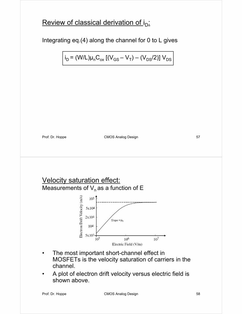
Velocity saturation effect:Measurements of Vn as a function of E
• The most important short-channel effect in MOSFETs is the velocity saturation of carriers in the channel.
• A plot of electron drift velocity versus electric field is shown above.
Prof. Dr. Hoppe CMOS Analog Design 59
Impact of velocity saturation (first impact):
Velocity of electrons as a function of E:
Vn = µnE
for E < Ec 1 + E/Ec
Vn = Vsat for E >= Ec
where Ec is the critical electric field at which velocity
saturation occurs
Inserting a factor in the equation of iD, we get:
iD = K(VDS)(W/L)µnCox [(VGS – VT) – (VDS/2)] VDS
Prof. Dr. Hoppe CMOS Analog Design 60
Impact of velocity saturation (first impact):
where
K(VDS) = 1
1 + VDS/EcL
is a SPICE parameter for modeling.
For L >> 1 µm, K(VDS) ~ 1
For short channel devices, K(VDS) < 1 resulting into
smaller iD than expected
Prof. Dr. Hoppe CMOS Analog Design 61
Impact of velocity saturation (second impact):
Short channel transistors enter the saturation region before VDS = VGS – VT
Assuming VDS is quite large,Vn = Vsat
iDsat = Vsat CoxW [VGS – VT – VDSsat]
iDsat = K(VDSsat)(W/L)µnCox [(VGS – VT) – (VDSsat/2)] VDSsat
Solving for VDSsat we get,
VDSsat = K(VGS – VT) [(VGS – VT)]
Prof. Dr. Hoppe CMOS Analog Design 62
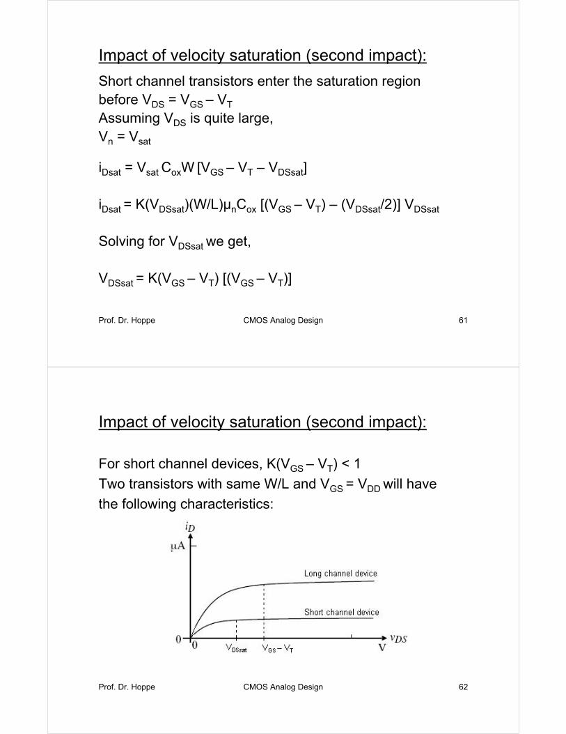
Impact of velocity saturation (second impact):
For short channel devices, K(VGS – VT) < 1
Two transistors with same W/L and VGS = VDD will have
the following characteristics:
Prof. Dr. Hoppe CMOS Analog Design 63
A simple model for hand calculations:
(1) Velocity saturation occurs abruptly at E = Ec
Vn = µnE for E < Ec
Vn = Vsat = µnEc for E >= Ec
(2) VDSsat at which Ec is reached is given as
VDSsat = LEc = LVsat /µn
(3) Approximate saturation current for a short channel
device is given as
iDsat = Vsat CoxW [VGS – VT – VDSsat]
Prof. Dr. Hoppe CMOS Analog Design 64
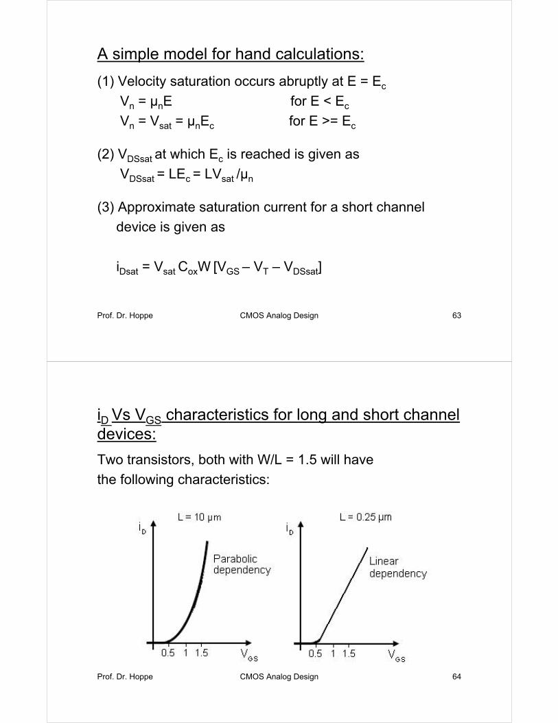
iD Vs VGS characteristics for long and short channel devices:
Two transistors, both with W/L = 1.5 will have
the following characteristics:
Prof. Dr. Hoppe CMOS Analog Design 65
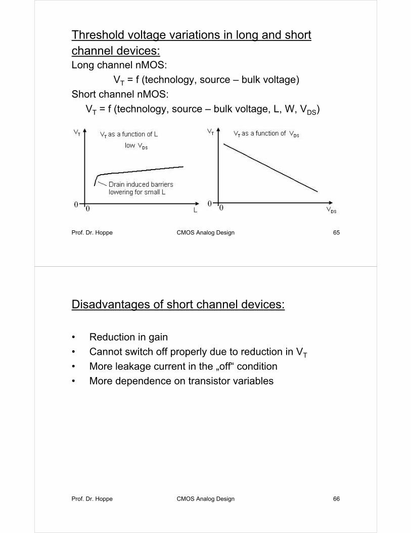
Threshold voltage variations in long and short channel devices:Long channel nMOS:
VT = f (technology, source – bulk voltage)
Short channel nMOS:
VT = f (technology, source – bulk voltage, L, W, VDS)
Prof. Dr. Hoppe CMOS Analog Design 66
Disadvantages of short channel devices:
• Reduction in gain
• Cannot switch off properly due to reduction in VT
• More leakage current in the „off“ condition
• More dependence on transistor variables
Prof. Dr. Hoppe CMOS Analog Design 67
Hot carrier effect:• During the last decade, transistor dimensions were
scaled down but not the power supply
• Increase in the field strength causes increase in the kinetic energy of electrons (hot electrons)
• Some of the electrons become so ‘hot‘ that they can jump over the barriers and tunnel into the oxide
• Electrons are trapped in the oxide and these additional charges increase VT of the transistors
• This leads to a long term reliability problem
• For an electron to become hot, a field strength greater than 104 V/cm is needed, which is easily possible for technologies with L < 1 µm
Prof. Dr. Hoppe CMOS Analog Design 68
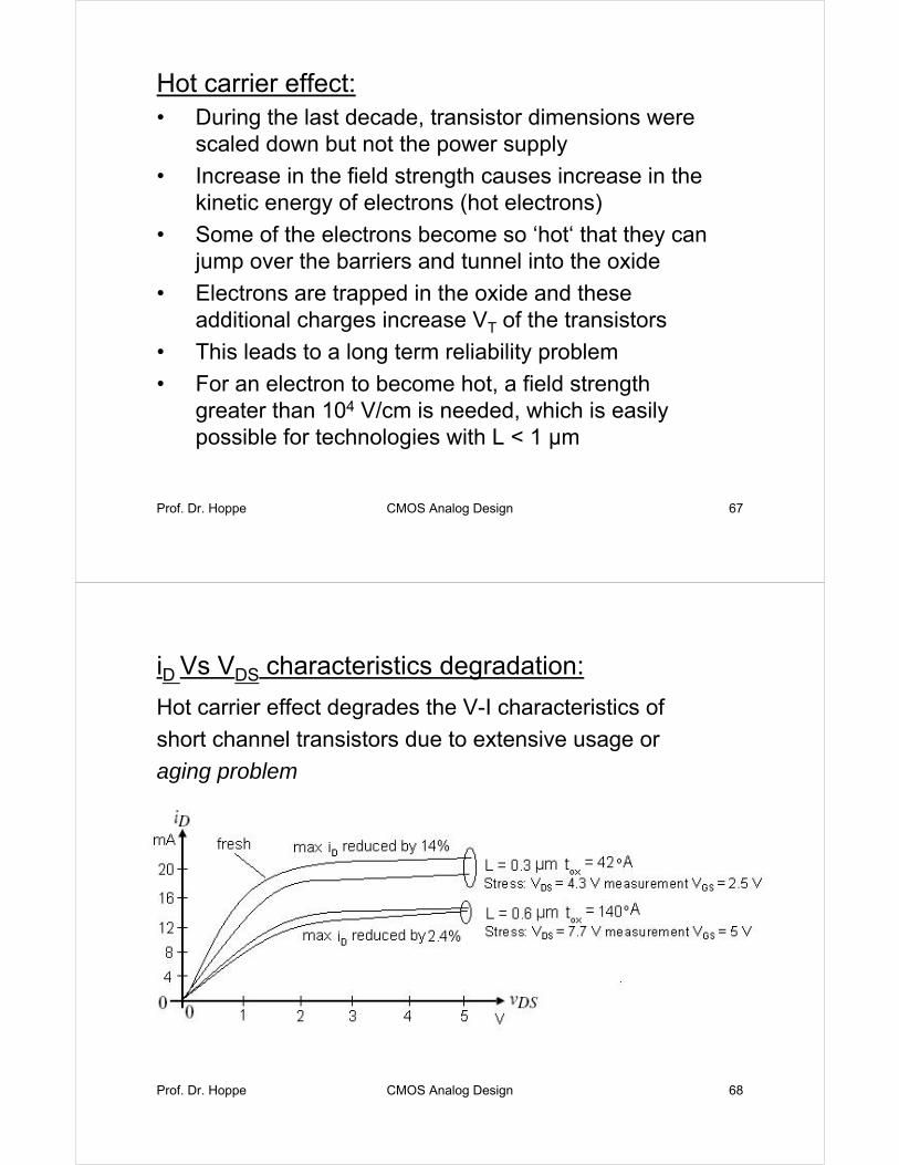
iD Vs VDS characteristics degradation:
Hot carrier effect degrades the V-I characteristics of
short channel transistors due to extensive usage or
aging problem
Prof. Dr. Hoppe CMOS Analog Design 69
Process variations:Device parameters vary between different wafer runs
and even on the same die!....why?
Answers :
(1) Variations of process parameters:
– impurity concentrations
– oxide thickness
– diffusion depths
(2) Temperature effects due to non uniform conditions:
– variations in sheet resistances
– variations in threshold voltages
– variations in parasitic capacitances
Prof. Dr. Hoppe CMOS Analog Design 70
Process variations:
(3) Variations in geometry of the devices:
– limited resolution of the lithographic processes results into variations in W/L ratios for the neighbouring transistors
– device mismatch in circuits built on the basis of transistor pairs, for ex: differential stages
Prof. Dr. Hoppe CMOS Analog Design 71
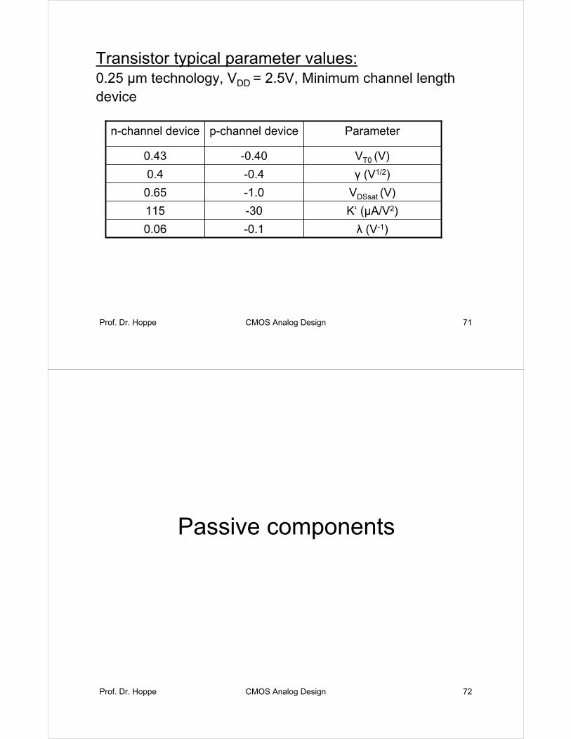
Transistor typical parameter values:0.25 µm technology, VDD = 2.5V, Minimum channel length device
VDSsat (V)-1.00.65
λ (V-1)-0.10.06
K‘ (µA/V2)-30115
γ (V1/2)-0.40.4
VT0 (V)-0.400.43
Parameterp-channel devicen-channel device
Prof. Dr. Hoppe CMOS Analog Design 72
Passive components
Prof. Dr. Hoppe CMOS Analog Design 73
Passive components for building analog circuits
in CMOS technology:
• MOS technology – planar technology
• Capacitors and resistors are compatible with MOS technology fabrication steps
• Inductors are not compatible
Prof. Dr. Hoppe CMOS Analog Design 74
Capacitors:
• Used more frequently in analog integrated circuits than in discrete designs
• Applications:
– compensation capacitors in amplifiers
– used in gain determining components in charge amplifiers
– charge storage devices in switched capacitor filters and digital to analog converters
Prof. Dr. Hoppe CMOS Analog Design 75
Desired characteristics for capacitors:
• Good matching accuracy
• Low voltage coefficient
• High ratio of desired capacitance to parasitic capacitance
• High capacitance per unit area
• Low temperature dependence
Note: Analog CMOS processes meet these criteria, pure digital processes do not!
Prof. Dr. Hoppe CMOS Analog Design 76
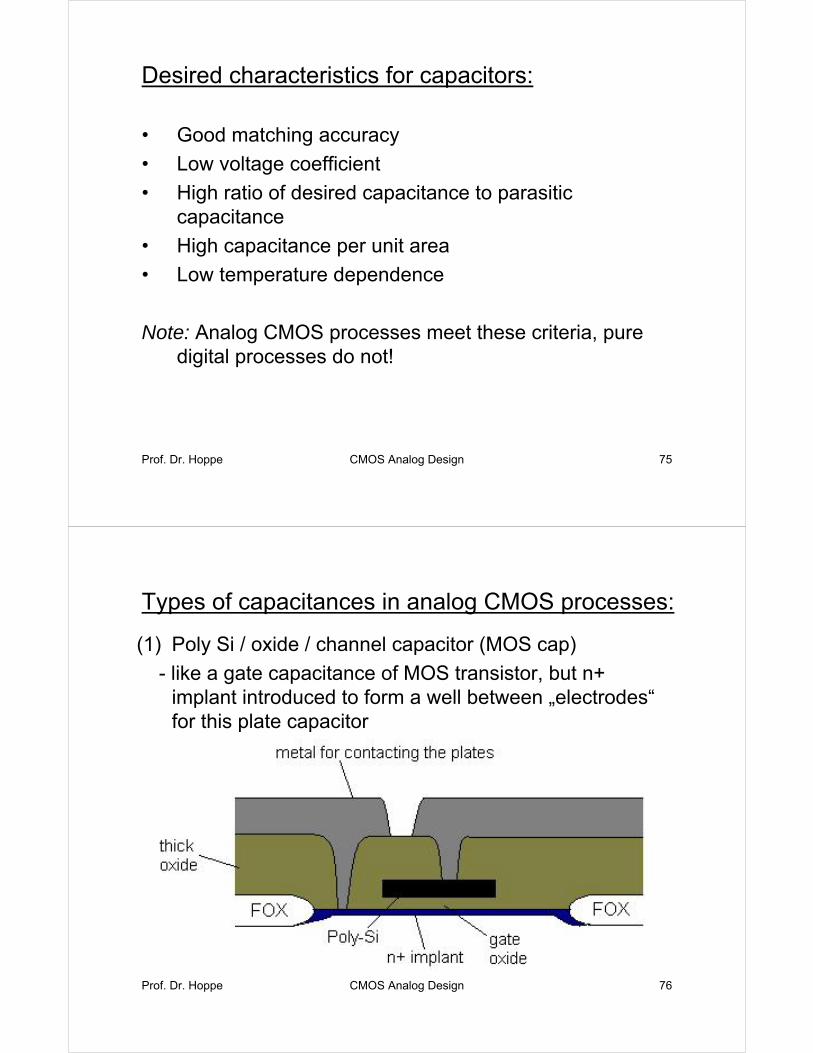
Types of capacitances in analog CMOS processes:
(1) Poly Si / oxide / channel capacitor (MOS cap)
- like a gate capacitance of MOS transistor, but n+ implant introduced to form a well between „electrodes“ for this plate capacitor
Prof. Dr. Hoppe CMOS Analog Design 77
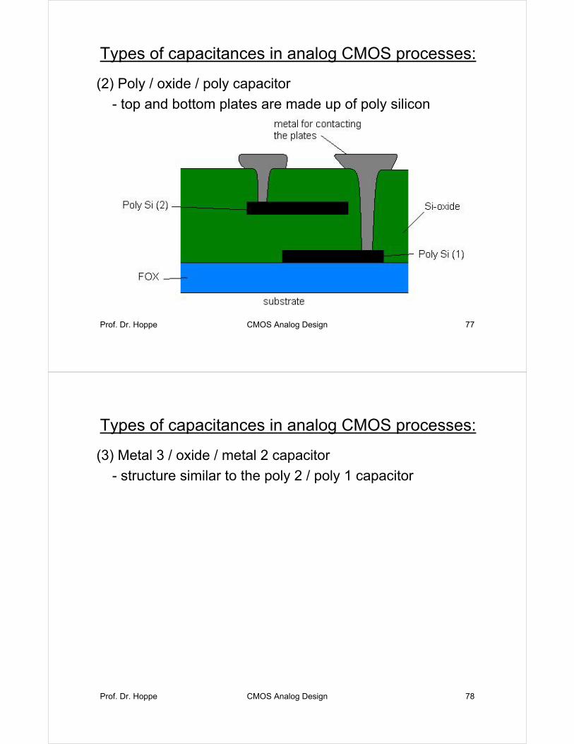
Types of capacitances in analog CMOS processes:
(2) Poly / oxide / poly capacitor
- top and bottom plates are made up of poly silicon
Prof. Dr. Hoppe CMOS Analog Design 78
Types of capacitances in analog CMOS processes:
(3) Metal 3 / oxide / metal 2 capacitor
- structure similar to the poly 2 / poly 1 capacitor
Prof. Dr. Hoppe CMOS Analog Design 79
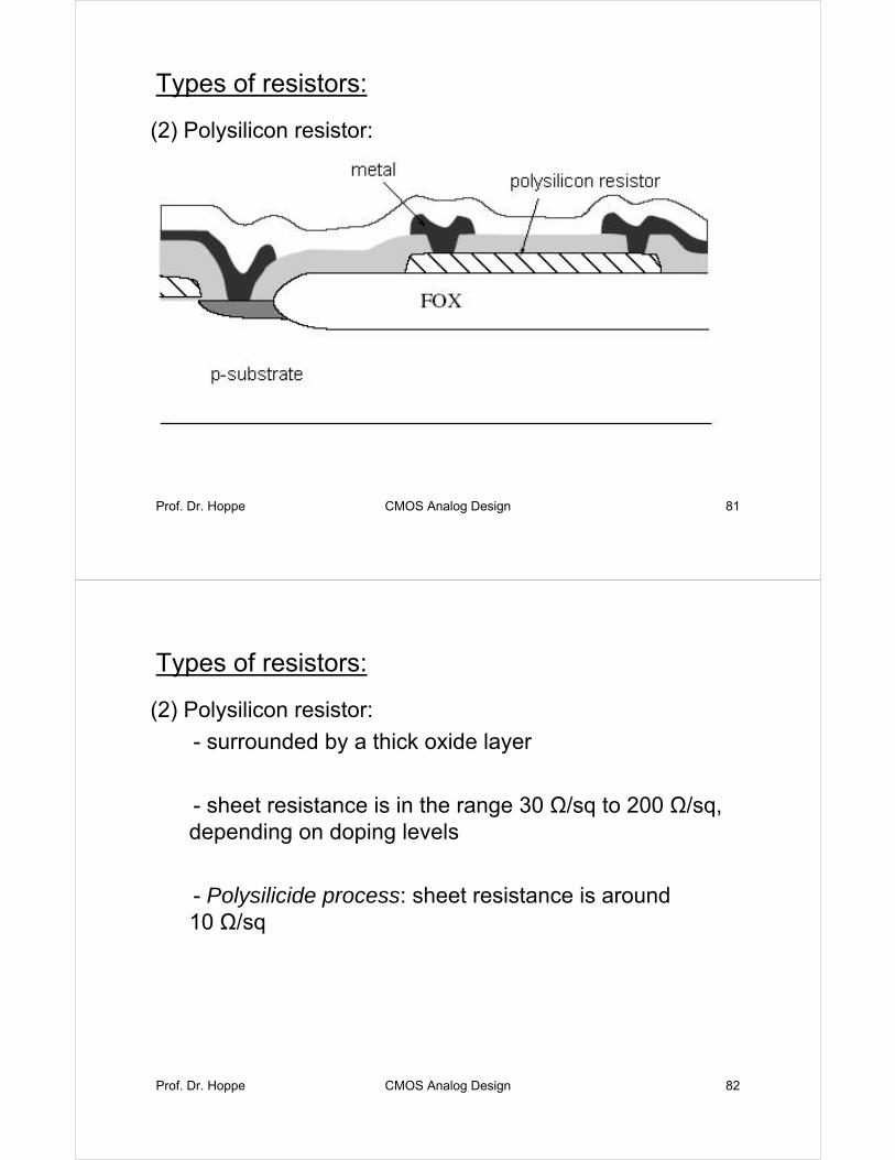
Types of resistors:
(1) Diffused resistor:
Prof. Dr. Hoppe CMOS Analog Design 80
Types of resistors:
(1) Diffused resistor:
- Standard process: sheet resistance is in the range 50 Ω/sq to 150 Ω/sq
- Salicided process: surface layer on silicon containing TaSi or TiSi compounds. Sheet resistance is in the range 5 Ω/sq to 15 Ω/sq
- Problems:
(a) capacitance to n-well
(b) voltage coefficient 100....250 ppm/V
Prof. Dr. Hoppe CMOS Analog Design 81
Types of resistors:
(2) Polysilicon resistor:
Prof. Dr. Hoppe CMOS Analog Design 82
Types of resistors:
(2) Polysilicon resistor:
- surrounded by a thick oxide layer
- sheet resistance is in the range 30 Ω/sq to 200 Ω/sq, depending on doping levels
- Polysilicide process: sheet resistance is around 10 Ω/sq
Prof. Dr. Hoppe CMOS Analog Design 83
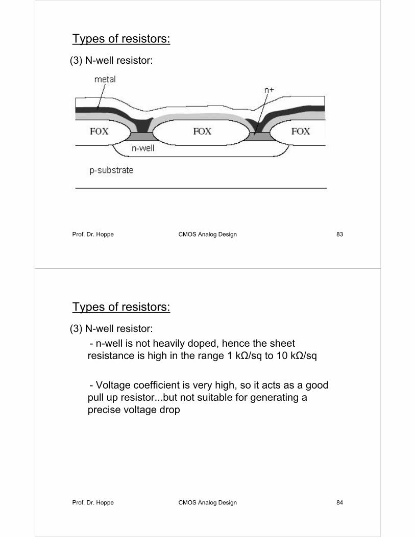
Types of resistors:
(3) N-well resistor:
Prof. Dr. Hoppe CMOS Analog Design 84
Types of resistors:
(3) N-well resistor:
- n-well is not heavily doped, hence the sheet resistance is high in the range 1 kΩ/sq to 10 kΩ/sq
- Voltage coefficient is very high, so it acts as a good pull up resistor...but not suitable for generating a precise voltage drop
Prof. Dr. Hoppe CMOS Analog Design 85
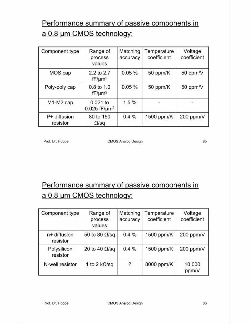
Performance summary of passive components in
a 0.8 µm CMOS technology:
0.4 %
1.5 %
0.05 %
0.05 %
Matching accuracy
80 to 150 Ω/sq
0.021 to 0.025 fF/µm2
0.8 to 1.0 fF/µm2
2.2 to 2.7 fF/µm2
Range of process values
--M1-M2 cap
200 ppm/V1500 ppm/KP+ diffusion resistor
50 ppm/V50 ppm/KPoly-poly cap
50 ppm/V50 ppm/KMOS cap
Voltage coefficient
Temperature coefficient
Component type
Prof. Dr. Hoppe CMOS Analog Design 86
Performance summary of passive components in
a 0.8 µm CMOS technology:
?
0.4 %
0.4 %
Matching accuracy
1 to 2 kΩ/sq
20 to 40 Ω/sq
50 to 80 Ω/sq
Range of process values
10,000 ppm/V
8000 ppm/KN-well resistor
200 ppm/V1500 ppm/KPolysilicon resistor
200 ppm/V1500 ppm/Kn+ diffusion resistor
Voltage coefficient
Temperature coefficient
Component type
Prof. Dr. Hoppe CMOS Analog Design 87
Temperature dependence of MOS devices
Prof. Dr. Hoppe CMOS Analog Design 88
Temperature dependence of MOS components:
• Temperature dependence of MOS components –important performance characteristic in analog circuit design
• The temperature behavior of passive components is usually expressed in terms of a fractional temperature coefficient TCF defined as:
TCF = 1.dXX dT
• X can be resistance or capacitance of the passive component. Usually TCF is multiplied by 106 and expressed in units of part per million per oC
Prof. Dr. Hoppe CMOS Analog Design 89
Temperature dependence of drain current iD of a MOS transistor:
• Most sensitive parameters in the drain current equation are µ (mobility) and VT (threshold voltage)
• Due to scattering at thermally induced lattice vibrations, temperature dependence of µ is given as
µ = KµT -1.5
• Temperature dependence of VT is approximated as
VT(T) = VT(T0) – α (T - T0)
α = 2.3 mV/oC and the expression is valid over the range 200 - 400 K
• Thus iD decreases with increasing temperature
iD | 125 oC = 0.7 iD | 25 oC
Prof. Dr. Hoppe CMOS Analog Design 90
Temperature dependence of reverse biased diode current:
• When VD < 0, the diode current is given as
-iD = Is = qA ( Dppn0 +Dnnp0 )=
qAD .(ni)2
Lp Ln L N
= KT3exp(- VG0 / Vt)
where D, L, N are diffusion constant, diffusion length and
impurity concentration of the dominant term (either n or p)
VG0 = band gap voltage of Si at 300 K (1.205V)Vt = thermal voltage kT/q
Prof. Dr. Hoppe CMOS Analog Design 91
Temperature dependence of reverse biased diode current:
• Differentiating with respect to T results indIs/dT = (3KT3/T)exp(-VG0 / Vt)
+ (qKT3VG0/KT2)exp(-VG0 / Vt)
= 3IS +
ISVG0
T TVt
• The TCF for the reverse diode current is
1 dIS = 3
+ VG0
IS dT T TVt
• Reverse diode current doubles for every 5 oC increase
Prof. Dr. Hoppe CMOS Analog Design 92
Example:
Calculate the TCF for the reverse diode current for 300 K
and Vt = 0.025 V
Prof. Dr. Hoppe CMOS Analog Design 93
Analog CMOS subcircuits
Prof. Dr. Hoppe CMOS Analog Design 94
MOS switch:• MOS switch – a very useful device
• Analog circuits: the MOS switch is used in multiplexers, modulation and switched capacitor filters
• Digital circuits: used in transmission gate logic, dynamic latches, etc.
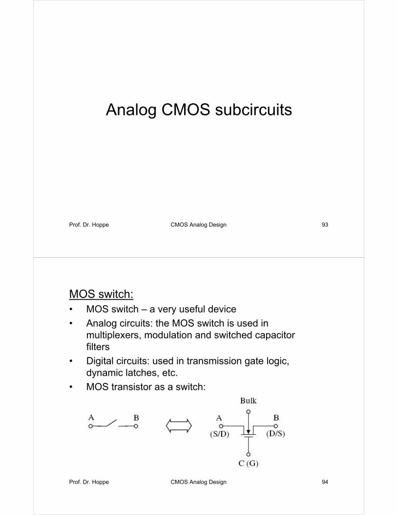
• MOS transistor as a switch:
Prof. Dr. Hoppe CMOS Analog Design 95
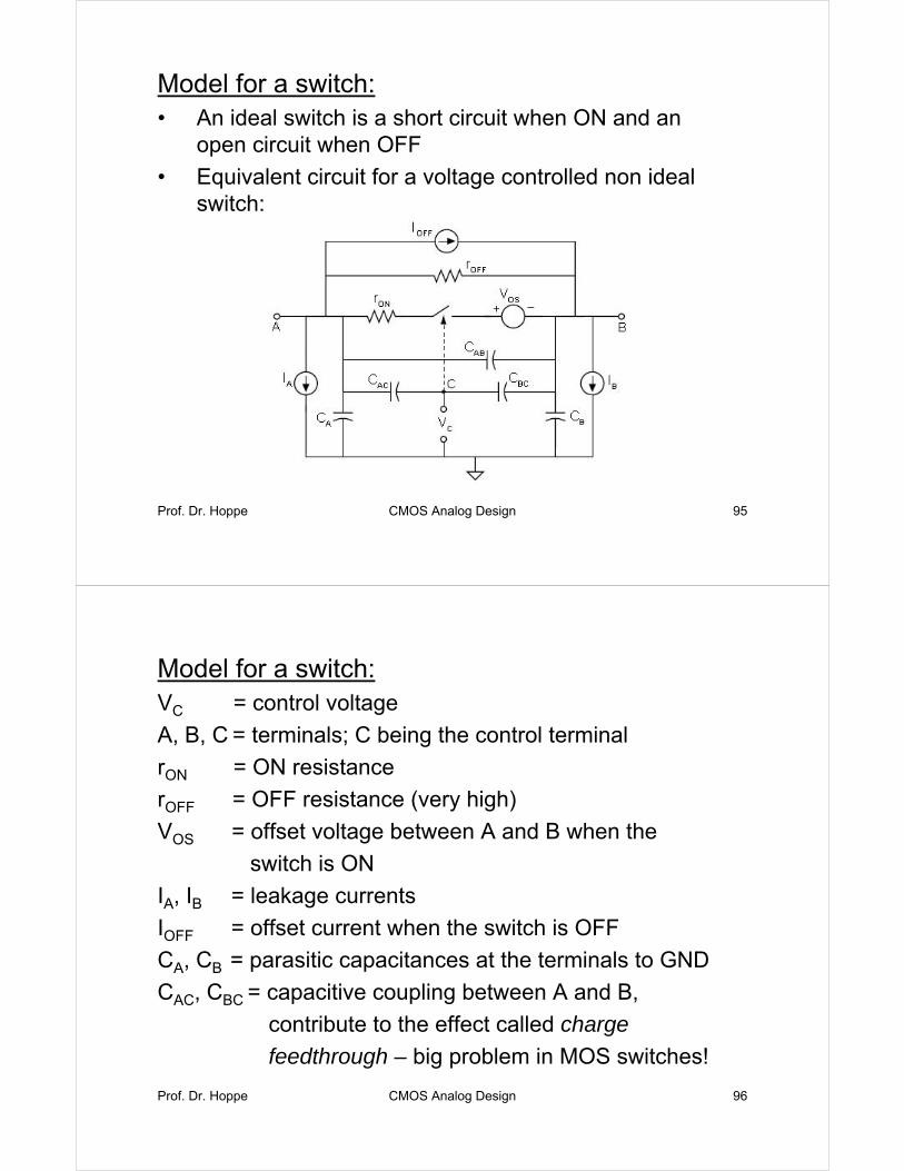
Model for a switch:• An ideal switch is a short circuit when ON and an
open circuit when OFF
• Equivalent circuit for a voltage controlled non ideal switch:
Prof. Dr. Hoppe CMOS Analog Design 96
Model for a switch:VC = control voltage
A, B, C = terminals; C being the control terminal
rON = ON resistance
rOFF = OFF resistance (very high)
VOS = offset voltage between A and B when the
switch is ON
IA, IB = leakage currents
IOFF = offset current when the switch is OFF
CA, CB = parasitic capacitances at the terminals to GND
CAC, CBC = capacitive coupling between A and B,
contribute to the effect called charge
feedthrough – big problem in MOS switches!
Prof. Dr. Hoppe CMOS Analog Design 97
ON resistance of a MOS switch:
• rON consists of the series combination of rD, rS and the channel resistance
• rD, rS – parasitic drain and source resistances (~ 1Ω)
• rchannel – channel resistance (~ 50Ω)....dominant!
• Expression for small-signal channel resistance:
rON = 1
= L
diD/dVDS Q K‘W(VGS - VT - VDS)
where Q designates the quiesent point of the transistor
Prof. Dr. Hoppe CMOS Analog Design 98
Range of voltages at the terminals of a MOS switch compared to the gate (control) voltage:
• nMOS: VG larger than the source to drain voltage to switch the transistor ON (atleast higher by VT)
• pMOS: VG has to be less than the source to drain voltage to switch the transistor ON
• nMOS: Bulk has to be connected to the most negative voltage
• pMOS: Bulk has to be connected to the most positive voltage
• Consider nMOS switch:VG = VDD , VBulk = VSS , then the transistor is ON untilVDD – VT >= VBA = VSD
Prof. Dr. Hoppe CMOS Analog Design 99
Single stage amplifiers
Prof. Dr. Hoppe CMOS Analog Design 100
Applications of CMOS amplifiers:
• Analog applications:
- to overcome noise
- to drive a next stage
- used in feedback systems
- to provide logic levels for interfacing to digital
circuits
• Digital applications:
- to drive a load
Prof. Dr. Hoppe CMOS Analog Design 101
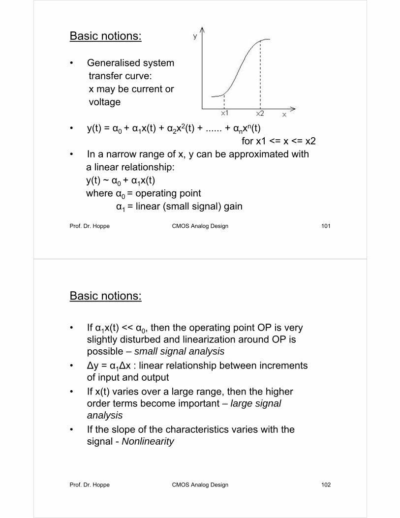
Basic notions:
• Generalised system transfer curve:x may be current orvoltage
• y(t) = α0 + α1x(t) + α2x2(t) + ...... + αnxn(t) for x1 <= x <= x2
• In a narrow range of x, y can be approximated with a linear relationship:y(t) ~ α0 + α1x(t)where α0 = operating point
α1 = linear (small signal) gain
Prof. Dr. Hoppe CMOS Analog Design 102
Basic notions:
• If α1x(t) << α0, then the operating point OP is very slightly disturbed and linearization around OP is possible – small signal analysis
• ∆y = α1∆x : linear relationship between increments of input and output
• If x(t) varies over a large range, then the higher order terms become important – large signal analysis
• If the slope of the characteristics varies with the signal - Nonlinearity
Prof. Dr. Hoppe CMOS Analog Design 103
Competing design targets for amplifiers:
1. Gain
2. Speed
3. Power consumption
4. Supply voltage
5. Linearity
6. Noise
7. Maximum voltage swing at the output
8. Input and output impedance
Prof. Dr. Hoppe CMOS Analog Design 104
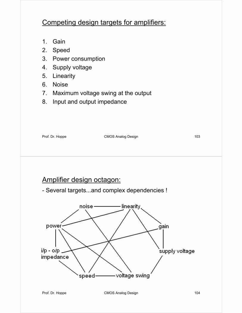
Amplifier design octagon:
- Several targets...and complex dependencies !
Prof. Dr. Hoppe CMOS Analog Design 105
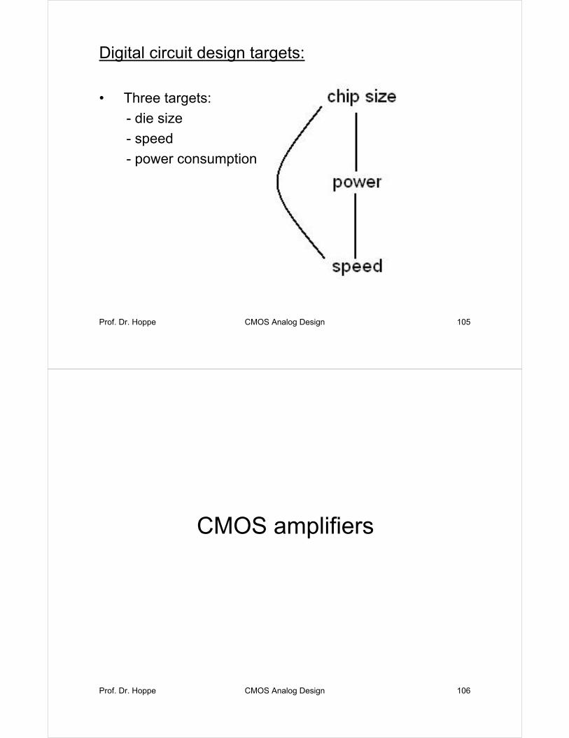
Digital circuit design targets:
• Three targets:
- die size
- speed
- power consumption
Prof. Dr. Hoppe CMOS Analog Design 106
CMOS amplifiers
Prof. Dr. Hoppe CMOS Analog Design 107
Basic principles:
• MOSFET translates variations in its gate-source voltage to a small signal drain current
• If a resistive load is used, these current variations in turn produce variations in the output voltage
Prof. Dr. Hoppe CMOS Analog Design 108
Amplifier configurations:
1. Common source stage (CS)
2. Source follower or common drain stage (SF)
3. Common gate stage (CG)
4. Cascode stage: cascade of CS and CG stage
5. Differential amplifiers
Prof. Dr. Hoppe CMOS Analog Design 109
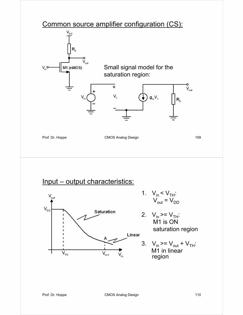
Common source amplifier configuration (CS):
Small signal model for the saturation region:
Prof. Dr. Hoppe CMOS Analog Design 110
Input – output characteristics:
1. Vin < VTH:Vout = VDD
2. Vin >= VTH:M1 is ONsaturation region
3. Vin >= Vout + VTH:M1 in linear region
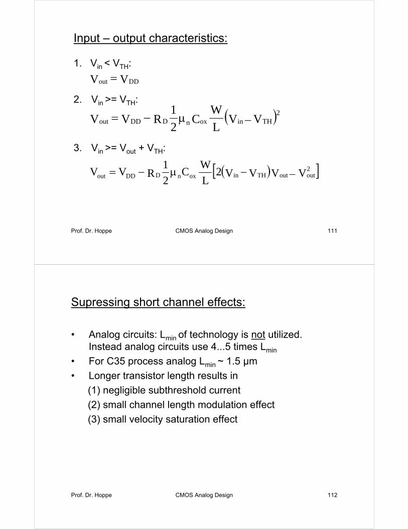
Prof. Dr. Hoppe CMOS Analog Design 111
Input – output characteristics:
1. Vin < VTH:
2. Vin >= VTH:
3. Vin >= Vout + VTH:
( )2THinoxnDDDout VVL
WC
2
1RVV −µ−=
( )[ ]VVVV2L
WC
2
1RVV 2
outoutTHinoxnDDDout −−µ−=
VV DDout =
Prof. Dr. Hoppe CMOS Analog Design 112
Supressing short channel effects:
• Analog circuits: Lmin of technology is not utilized. Instead analog circuits use 4...5 times Lmin
• For C35 process analog Lmin ~ 1.5 µm
• Longer transistor length results in
(1) negligible subthreshold current
(2) small channel length modulation effect
(3) small velocity saturation effect
Prof. Dr. Hoppe CMOS Analog Design 113
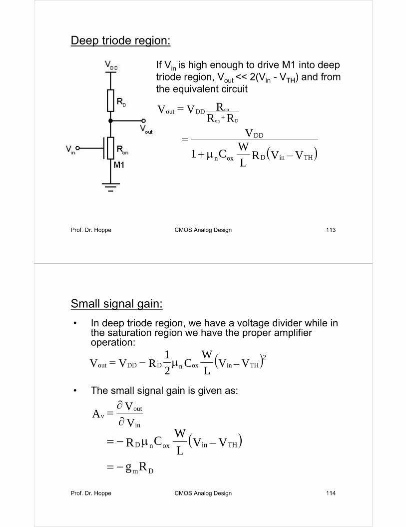
Deep triode region:
If Vin is high enough to drive M1 into deep triode region, Vout << 2(Vin - VTH) and from the equivalent circuit
VRR
RVDon
onDDout+
=
( )VVRLW
C1
V
THinDoxn
DD
−µ+=
Prof. Dr. Hoppe CMOS Analog Design 114
Small signal gain:
( )2THinoxnDDDout VVL
WC
2
1RVV −µ−=
• In deep triode region, we have a voltage divider while in the saturation region we have the proper amplifier operation:
• The small signal gain is given as:
V
VA
in
out
∂∂
=ν
( )VVL
WCR THinoxnD −µ−=
DmRg−=
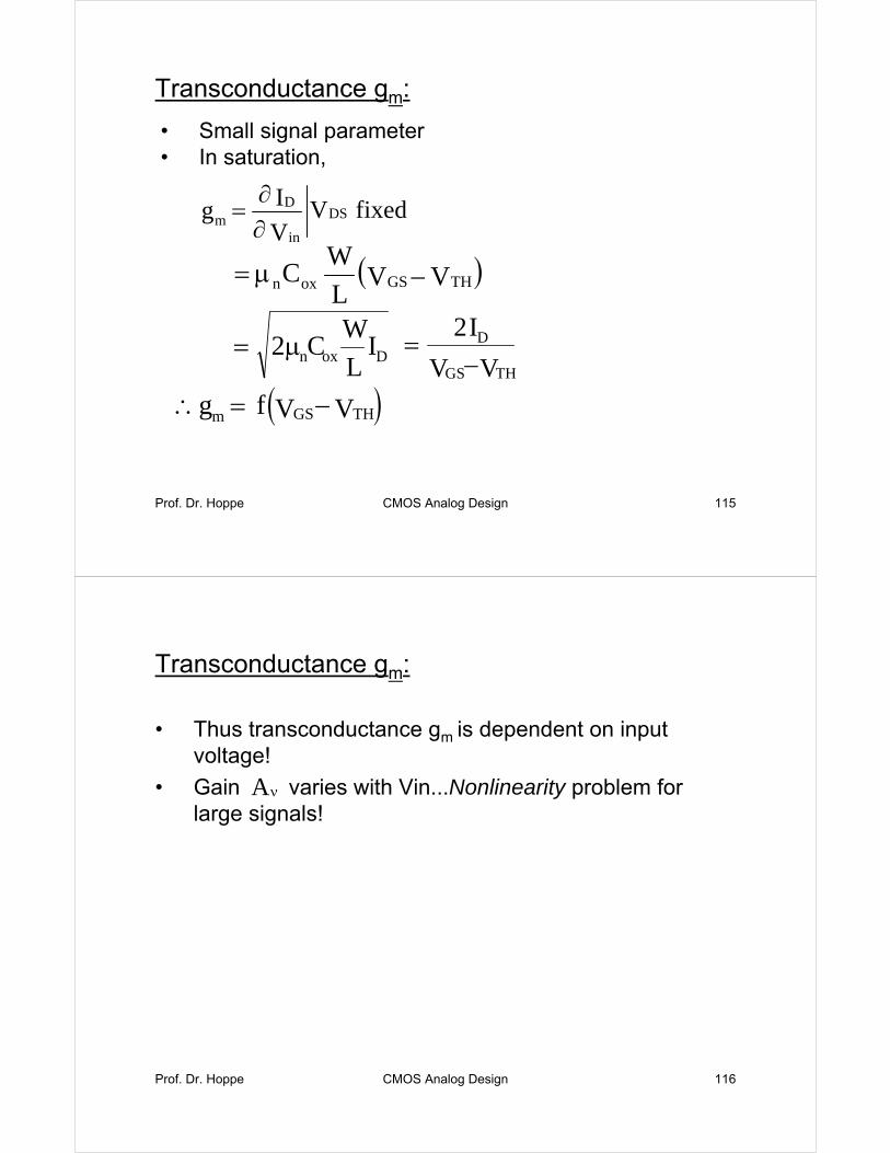
Prof. Dr. Hoppe CMOS Analog Design 115
• Small signal parameter• In saturation,
Transconductance gm:
( )VVL
WC THGSoxn −µ=
fixedVV
Ig DS
in
Dm ∂
∂=
Doxn IL
WC2µ=
VV
I2
THGS
D
−=
( )VVfg THGSm −=∴
Prof. Dr. Hoppe CMOS Analog Design 116
Transconductance gm:
• Thus transconductance gm is dependent on input voltage!
• Gain varies with Vin...Nonlinearity problem for large signals!
Aν

Prof. Dr. Hoppe CMOS Analog Design 117
How to maximize the voltage gain?
Where VRD is voltage drop across load resistance
• To increase the gain:- make W/L larger- make VRD large.... make RD large - make ID smaller (make transistor weaker)
I
VI
L
WC2A
D
RDDoxn ∗µ−=ν
I
VL
WC2A
D
RDoxn ∗µ−=ν
Prof. Dr. Hoppe CMOS Analog Design 118
Trade-offs in maximizing the voltage gain:
• Larger W/L larger input capacitance• Larger VRD smaller output swing• If VRD is kept constant ID has to be made smaller
RD must be increasedhigher time constants at the output !
• Trade-off: gain, BW, voltage swing !
⇒⇒
⇒
⇒⇒
Prof. Dr. Hoppe CMOS Analog Design 119
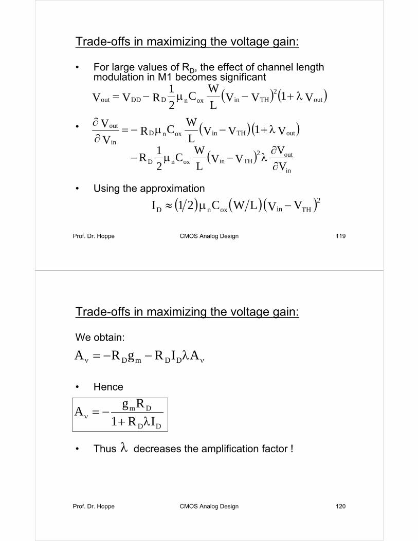
Trade-offs in maximizing the voltage gain:
• For large values of RD, the effect of channel length modulation in M1 becomes significant
•
• Using the approximation
( ) ( )V1VVL
WC
2
1RVV out
2THinoxnDDDout λ+−µ−=
( ) ( )V1VVL
WCR
V
VoutTHinoxnD
in
out λ+−µ−=∂∂
( )in
out2THinoxnD V
VVV
L
WC
2
1R
∂∂
λ−µ−
( ) ( ) ( )2THinoxnD VVLWC21I −µ≈
Prof. Dr. Hoppe CMOS Analog Design 120
Trade-offs in maximizing the voltage gain:
We obtain:
• Hence
• Thus decreases the amplification factor !
DD
Dm
IR1
RgA
λ+−=ν
νν λ−−= AIRgRA DDmD
λ
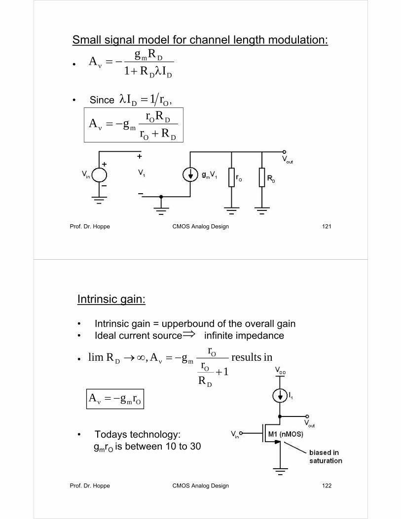
Prof. Dr. Hoppe CMOS Analog Design 121
Small signal model for channel length modulation:
•
• Since ,
DD
Dm
IR1
RgA
λ+−=ν
OD r1I =λ
DO
DOm Rr
RrgA
+−=ν
Prof. Dr. Hoppe CMOS Analog Design 122
Intrinsic gain:
• Intrinsic gain = upperbound of the overall gain• Ideal current source infinite impedance
•
• Todays technology:gmrO is between 10 to 30
Om
D
O
OmD
rgA
inresults1
Rr
rgA,Rlim
−=
+−=∞→
ν
ν
⇒
Prof. Dr. Hoppe CMOS Analog Design 123
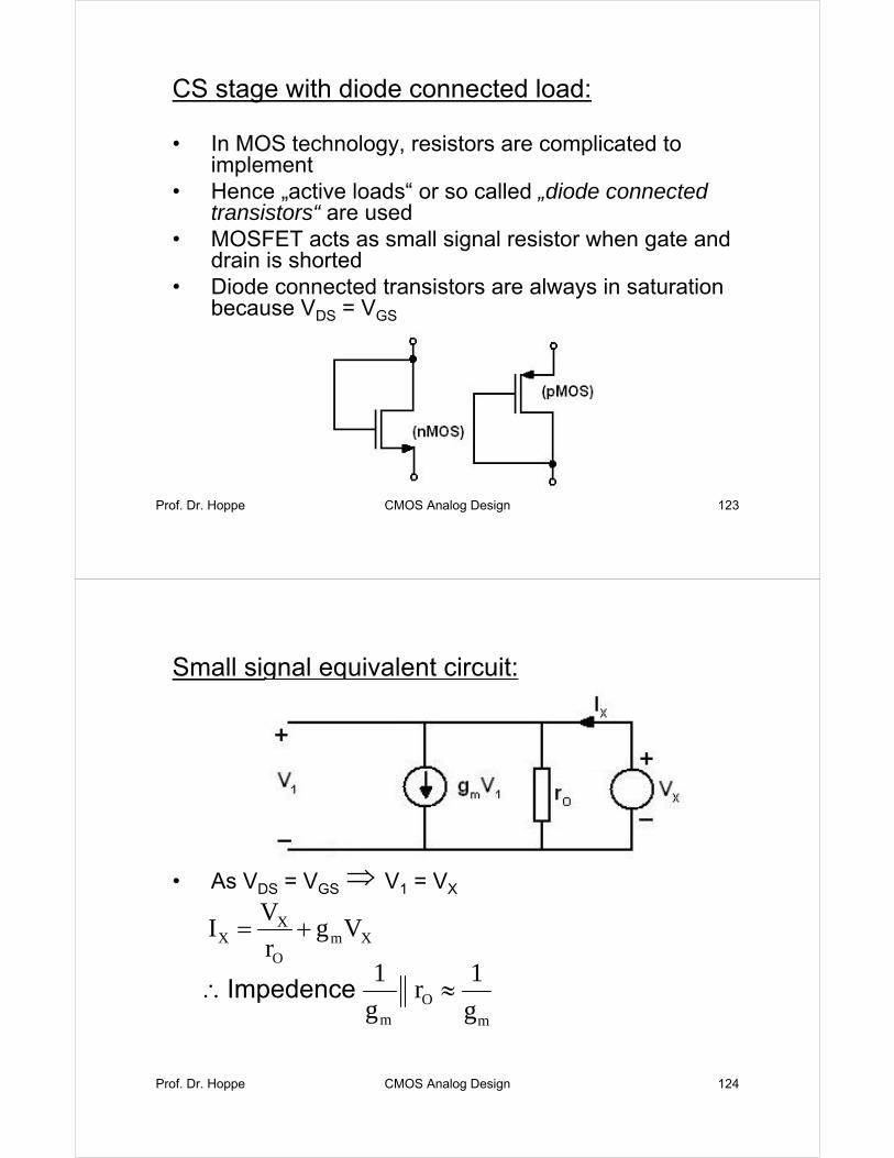
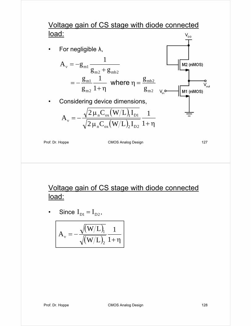
CS stage with diode connected load:
• In MOS technology, resistors are complicated to implement
• Hence „active loads“ or so called „diode connected transistors“ are used
• MOSFET acts as small signal resistor when gate and drain is shorted
• Diode connected transistors are always in saturation because VDS = VGS
Prof. Dr. Hoppe CMOS Analog Design 124
Small signal equivalent circuit:
• As VDS = VGS V1 = VX ⇒
XmO
XX Vg
r
VI +=
g
1r
g
1
m
Om
≈∴ Impedence
Prof. Dr. Hoppe CMOS Analog Design 125
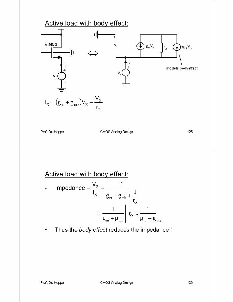
Active load with body effect:
⇔
( )O
XXmbmX r
VVggI ++=
Prof. Dr. Hoppe CMOS Analog Design 126
Active load with body effect:
•
• Thus the body effect reduces the impedance !
Ombm r
1gg
1
++==
X
X
I
V Impedance
mbmO
mbm gg
1r
gg
1
+≈
+=
Prof. Dr. Hoppe CMOS Analog Design 127
Voltage gain of CS stage with diode connected load:
• For negligible λ,
• Considering device dimensions,
2mb2m1m gg
1gA
+−=ν
2m
2mb
2m
1m
g
g
1
1
g
g=η
η+−= where
( )( ) η+µ
µ−=ν 1
1
ILWC2
ILWC2A
2D2oxn
1D1oxn
Prof. Dr. Hoppe CMOS Analog Design 128
Voltage gain of CS stage with diode connected load:
• Since ,
( )( ) η+
−=ν 1
1
LW
LWA
2
1
2D1D II =
Prof. Dr. Hoppe CMOS Analog Design 129
CS stage with diode connected load – Large signal analysis:
•
Note: If VTH2 depends only slightly on Vout (weak body effect), then we have a linear behavior and Vout is proportional to Vin
2D1D II =
( ) ( )22THoutDD2
oxn2
1THin1
oxn VVVL
WC
2
1VV
L
WC
2
1−−⎟
⎠⎞
⎜⎝⎛µ=−⎟
⎠⎞
⎜⎝⎛µ∴
( ) ( )2THoutDD2
1THin1
VVVL
WVV
L
W−−⎟
⎠⎞
⎜⎝⎛=−⎟
⎠⎞
⎜⎝⎛∴
Prof. Dr. Hoppe CMOS Analog Design 130
CS stage with diode connected load – Large signal analysis:
• Differentiating both sides w.r.t Vin
• With application of the chain rule
we getThe result matches with the small signal analysis !
⎟⎟⎠
⎞⎜⎜⎝
⎛∂∂
−∂∂
−⎟⎠⎞
⎜⎝⎛=⎟
⎠⎞
⎜⎝⎛
in
2TH
in
out
21 V
V
V
V
L
W
L
W
⎟⎟⎠
⎞⎜⎜⎝
⎛∂∂
η=⎟⎟⎠
⎞⎜⎜⎝
⎛∂∂
⎟⎟⎠
⎞⎜⎜⎝
⎛∂∂
=∂∂
in
out
in
out
out
2TH
in
2TH
V
V
V
V
V
V
V
V
( )( ) η+
−=∂∂
=ν 1
1
LW
LW
V
VA
2
1
in
out
Prof. Dr. Hoppe CMOS Analog Design 131
Input / output characteristics of active load CS stage:
• At point A, M1 enters the triode region (strong nonlinearity !)
• Above VTH1 and below VA,(linear behavior) inout VV ∝
Prof. Dr. Hoppe CMOS Analog Design 132
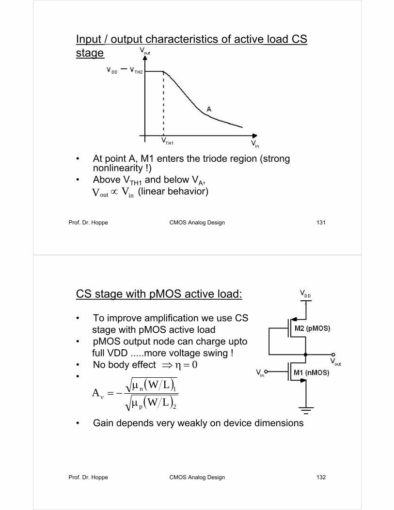
CS stage with pMOS active load:
• To improve amplification we use CS stage with pMOS active load
• pMOS output node can charge uptofull VDD .....more voltage swing !
• No body effect•
• Gain depends very weakly on device dimensions
0=η⇒
( )( )2p
1n
LW
LWA
µ
µ−=ν
Prof. Dr. Hoppe CMOS Analog Design 133
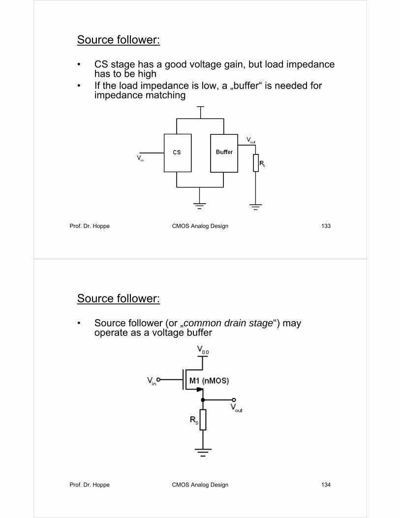
Source follower:
• CS stage has a good voltage gain, but load impedance has to be high
• If the load impedance is low, a „buffer“ is needed for impedance matching
Prof. Dr. Hoppe CMOS Analog Design 134
Source follower:
• Source follower (or „common drain stage“) may operate as a voltage buffer
Prof. Dr. Hoppe CMOS Analog Design 135
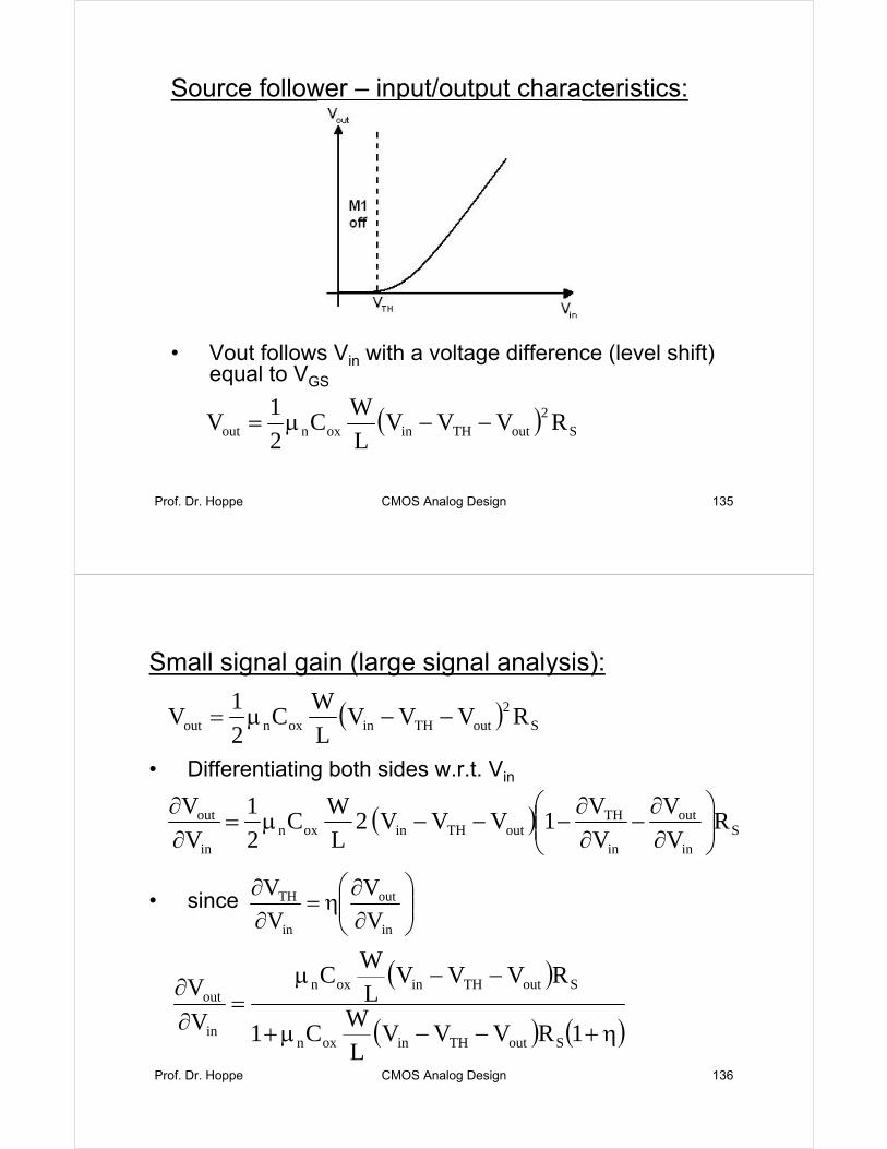
Source follower – input/output characteristics:
• Vout follows Vin with a voltage difference (level shift) equal to VGS
( ) S2
outTHinoxnout RVVVL
WC
2
1V −−µ=
Prof. Dr. Hoppe CMOS Analog Design 136
Small signal gain (large signal analysis):
• Differentiating both sides w.r.t. Vin
• since
( ) S2
outTHinoxnout RVVVL
WC
2
1V −−µ=
( ) Sin
out
in
THoutTHinoxn
in
out RV
V
V
V1VVV2
L
WC
2
1
V
V⎟⎟⎠
⎞⎜⎜⎝
⎛∂∂
−∂∂
−−−µ=∂∂
⎟⎟⎠
⎞⎜⎜⎝
⎛∂∂
η=∂∂
in
out
in
TH
V
V
V
V
( )
( ) ( )η+−−µ+
−−µ=
∂∂
1RVVVLW
C1
RVVVLW
C
V
V
SoutTHinoxn
SoutTHinoxn
in
out
Prof. Dr. Hoppe CMOS Analog Design 137
Small signal gain (large signal analysis):
• With we get:( )outTHinoxnm VVVL
WCg −−µ=
( ) Smbm
Sm
Rgg1
RgA
++=ν
Prof. Dr. Hoppe CMOS Analog Design 138
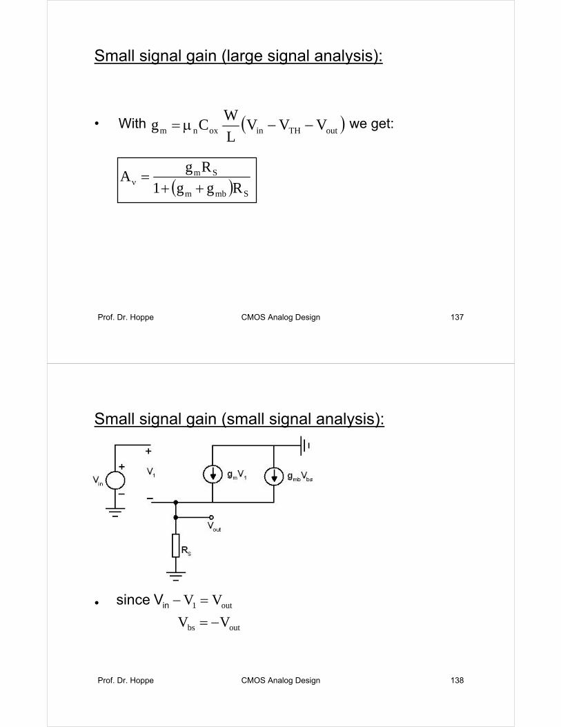
Small signal gain (small signal analysis):
•
outbs
out1
VV
VV
−==−in Vsince
Prof. Dr. Hoppe CMOS Analog Design 139
Small signal gain (small signal analysis):
•
will result in
• Maximum possible gain = 1
S
outout1mb11m R
VVgVg =−
in
out
V
VA =ν
( ) Smbm
Sm
Rgg1
RgA
++=ν
Prof. Dr. Hoppe CMOS Analog Design 140
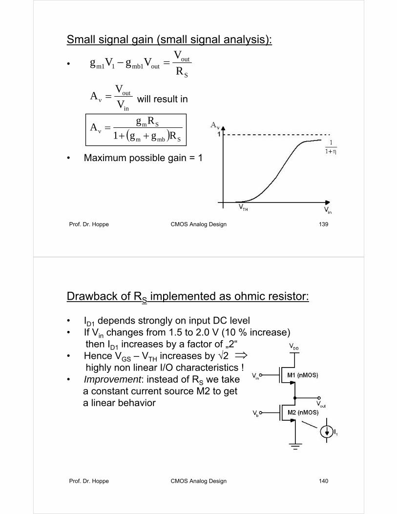
Drawback of RS implemented as ohmic resistor:
• ID1 depends strongly on input DC level• If Vin changes from 1.5 to 2.0 V (10 % increase)
then ID1 increases by a factor of „2“• Hence VGS – VTH increases by √2
highly non linear I/O characteristics !• Improvement: instead of RS we take
a constant current source M2 to get a linear behavior
⇒
Prof. Dr. Hoppe CMOS Analog Design 141
Output impedance of SF with constant current source as load:
•
⇔
X1 VV −=
0VgVgI XmbXmX =−−∴
Prof. Dr. Hoppe CMOS Analog Design 142
Output impedance of SF with constant current source as load:
•
• Note: Body effect decreases the output resistance of the source follower !
mbmout
X
X
gg
1R
I
V
+== Hence
Prof. Dr. Hoppe CMOS Analog Design 143
Example: Source follower:W/L = 20µm/0.5µmVTH0 = 0.6 V|2ΦF| = 0.7 VµnCox = 50 µA/V2
γ = 0.4 V2
I1 = 200 µA
Q1: What is Vout for Vin = 1.2 V?Q2: If I1 is produced by an nMOS device, what is the
minimum W/L ratio for which M2 remains saturated?
Prof. Dr. Hoppe CMOS Analog Design 144
Solution A1:
• VTH depends on Vout
Iterative solution: (1) we calculate Vout for VTH0
(2) we calculate VTH for Vout obtained in (1)
( )2outTHinoxnD VVVL
WC
2
1I −−⎟
⎠⎞
⎜⎝⎛µ=
( )
LW
C
I2VVV
oxn
D2outTHin
µ=−−∴
( )40*A50
A200*2V6.02.1 2
out µµ
=−−∴
Prof. Dr. Hoppe CMOS Analog Design 145
Solution A1:
• Now,
• Using the new VTH the improved value of Vout is 0.119 V, which is approximately 35 mV less than the calculated value.
V153.0Vout =∴
( )FSBF0THTH 2V2VV φ−+φγ+=
( )7.0153.07.04.06.0VTH −++=∴
V635.0=
Prof. Dr. Hoppe CMOS Analog Design 146
Solution A2:
• Consider transistor in place of current source:• Drain-source voltage of M2 is 0.119 V• Device is saturated only if VGS – VTH < 0.119 V• In the saturation region we have,
( )22
oxnD 119.0L
WC
2
1A200I ⎟
⎠⎞
⎜⎝⎛µ=µ=
m5.0
m283
L
W
min2 µµ
=⎟⎠⎞
⎜⎝⎛∴
Prof. Dr. Hoppe CMOS Analog Design 147
Drawbacks of the SF configuration:
• Source followers exhibit a high input impedance and a moderate output impedance, but at the cost of two drawbacks:
(1) nonlinearity(2) voltage headroom limitation
Prof. Dr. Hoppe CMOS Analog Design 148
Nonlinearity of the SF configuration:
• Even with an ideal current source I1 the I/O characteristics display a nonlinearity due to the dependence of VTH on Vsource
• Submicron technology: rO of the transistor also changes with VDS additional nonlinear effects !
• Nonlinearity due to body effect can be eliminated if the bulk is tied to the source
• Because all nMOS devices have a common bulk potential, this is only possible for pMOS devices in a n-well technology
⇒
Prof. Dr. Hoppe CMOS Analog Design 149
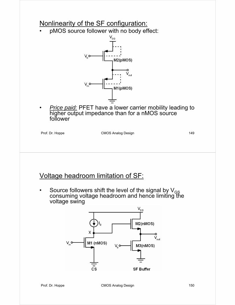
Nonlinearity of the SF configuration: • pMOS source follower with no body effect:
• Price paid: PFET have a lower carrier mobility leading to higher output impedance than for a nMOS source follower
Prof. Dr. Hoppe CMOS Analog Design 150
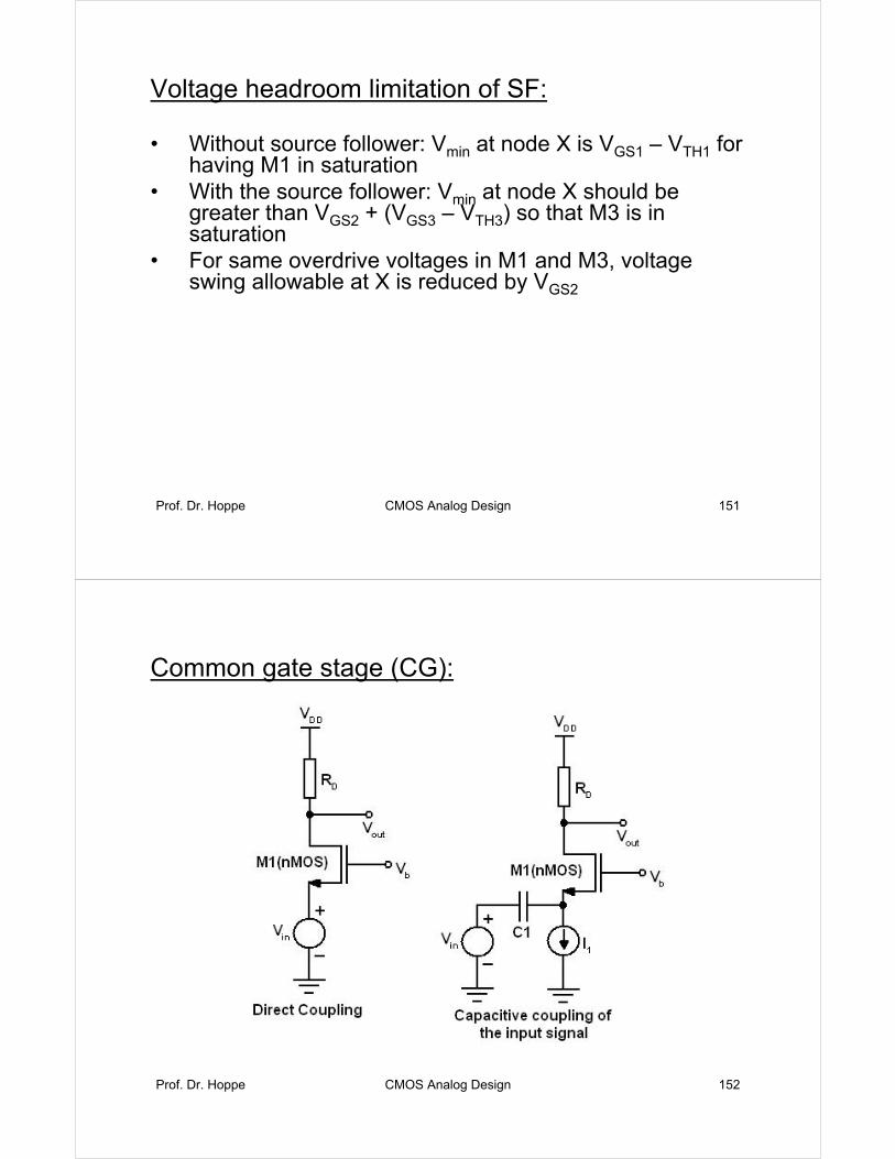
Voltage headroom limitation of SF:
• Source followers shift the level of the signal by VGSconsuming voltage headroom and hence limiting the voltage swing
Prof. Dr. Hoppe CMOS Analog Design 151
Voltage headroom limitation of SF:
• Without source follower: Vmin at node X is VGS1 – VTH1 for having M1 in saturation
• With the source follower: Vmin at node X should be greater than VGS2 + (VGS3 – VTH3) so that M3 is in saturation
• For same overdrive voltages in M1 and M3, voltage swing allowable at X is reduced by VGS2
Prof. Dr. Hoppe CMOS Analog Design 152
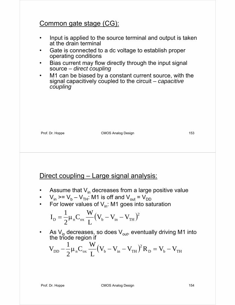
Common gate stage (CG):
Prof. Dr. Hoppe CMOS Analog Design 153
Common gate stage (CG):
• Input is applied to the source terminal and output is taken at the drain terminal
• Gate is connected to a dc voltage to establish proper operating conditions
• Bias current may flow directly through the input signal source – direct coupling
• M1 can be biased by a constant current source, with the signal capacitively coupled to the circuit – capacitive coupling
Prof. Dr. Hoppe CMOS Analog Design 154
Direct coupling – Large signal analysis:
• Assume that Vin decreases from a large positive value• Vin >= Vb – VTH: M1 is off and Vout = VDD
• For lower values of Vin: M1 goes into saturation
• As Vin decreases, so does Vout, eventually driving M1 into the triode region if
( )2THinboxnD VVVL
WC
2
1I −−µ=
( ) THbD2
THinboxnDD VVRVVVL
WC
2
1V −=−−µ−
Prof. Dr. Hoppe CMOS Analog Design 155
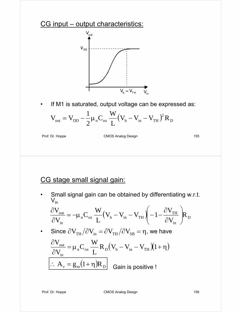
CG input – output characteristics:
• If M1 is saturated, output voltage can be expressed as:
( ) D2
THinboxnDDout RVVVL
WC
2
1VV −−µ−=
Prof. Dr. Hoppe CMOS Analog Design 156
CG stage small signal gain:
• Small signal gain can be obtained by differentiating w.r.t. Vin
• Since , we have
Gain is positive !
( ) Din
THTHinboxn
in
out RV
V1VVV
L
WC
V
V⎟⎟⎠
⎞⎜⎜⎝
⎛∂∂
−−−−µ−=∂∂
η=∂∂=∂∂ SBTHinTH VVVV
( )( )η+−−µ=∂∂
1VVVRL
WC
V
VTHinbDoxn
in
out
( ) Dm R1gA η+=∴ ν
Prof. Dr. Hoppe CMOS Analog Design 157
CG stage input impedance:
• For λ = 0, the impedance seen at the source of M1 is like in the case of source follower
• Thus, the body effect decreases the input impedance !
( )η+=+ 1g
1
gg
1
mmbm
Prof. Dr. Hoppe CMOS Analog Design 158
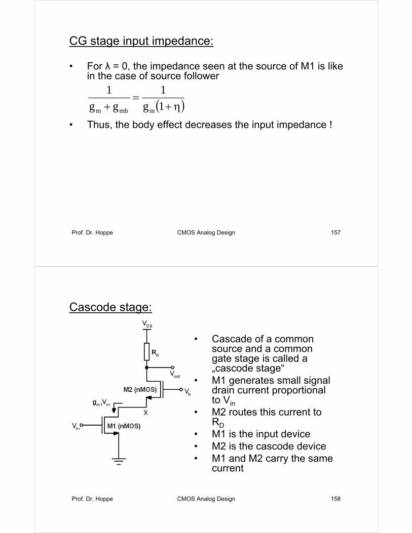
Cascode stage:
• Cascade of a common source and a common gate stage is called a „cascode stage“
• M1 generates small signal drain current proportional to Vin
• M2 routes this current to RD
• M1 is the input device• M2 is the cascode device• M1 and M2 carry the same
current
Prof. Dr. Hoppe CMOS Analog Design 159
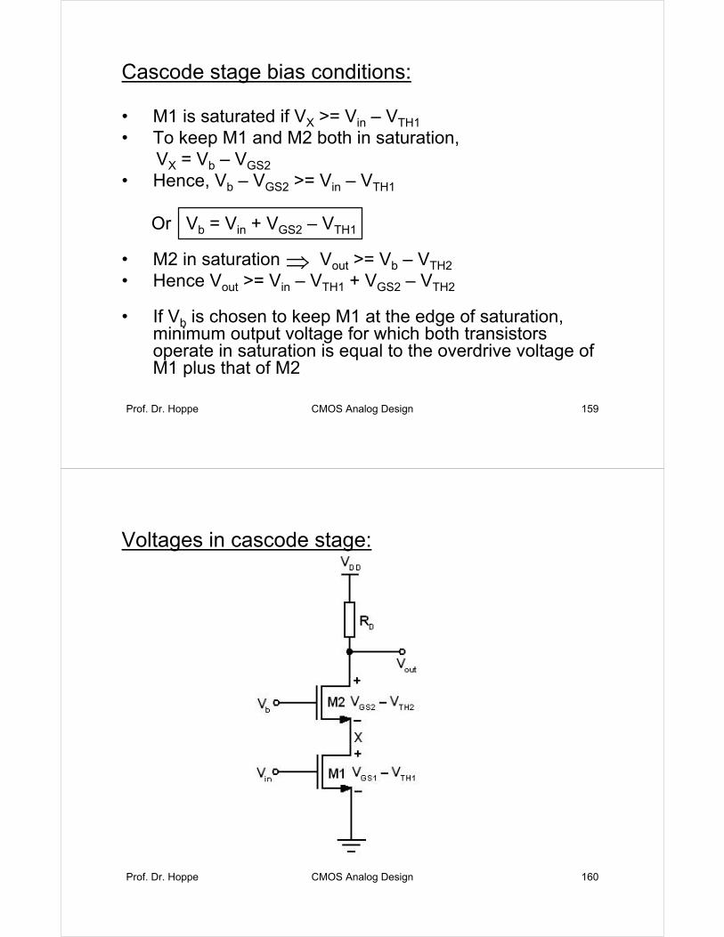
Cascode stage bias conditions:
• M1 is saturated if VX >= Vin – VTH1
• To keep M1 and M2 both in saturation,VX = Vb – VGS2
• Hence, Vb – VGS2 >= Vin – VTH1
Or Vb = Vin + VGS2 – VTH1
• M2 in saturation Vout >= Vb – VTH2
• Hence Vout >= Vin – VTH1 + VGS2 – VTH2
• If Vb is chosen to keep M1 at the edge of saturation, minimum output voltage for which both transistors operate in saturation is equal to the overdrive voltage of M1 plus that of M2
⇒
Prof. Dr. Hoppe CMOS Analog Design 160
Voltages in cascode stage:
Prof. Dr. Hoppe CMOS Analog Design 161
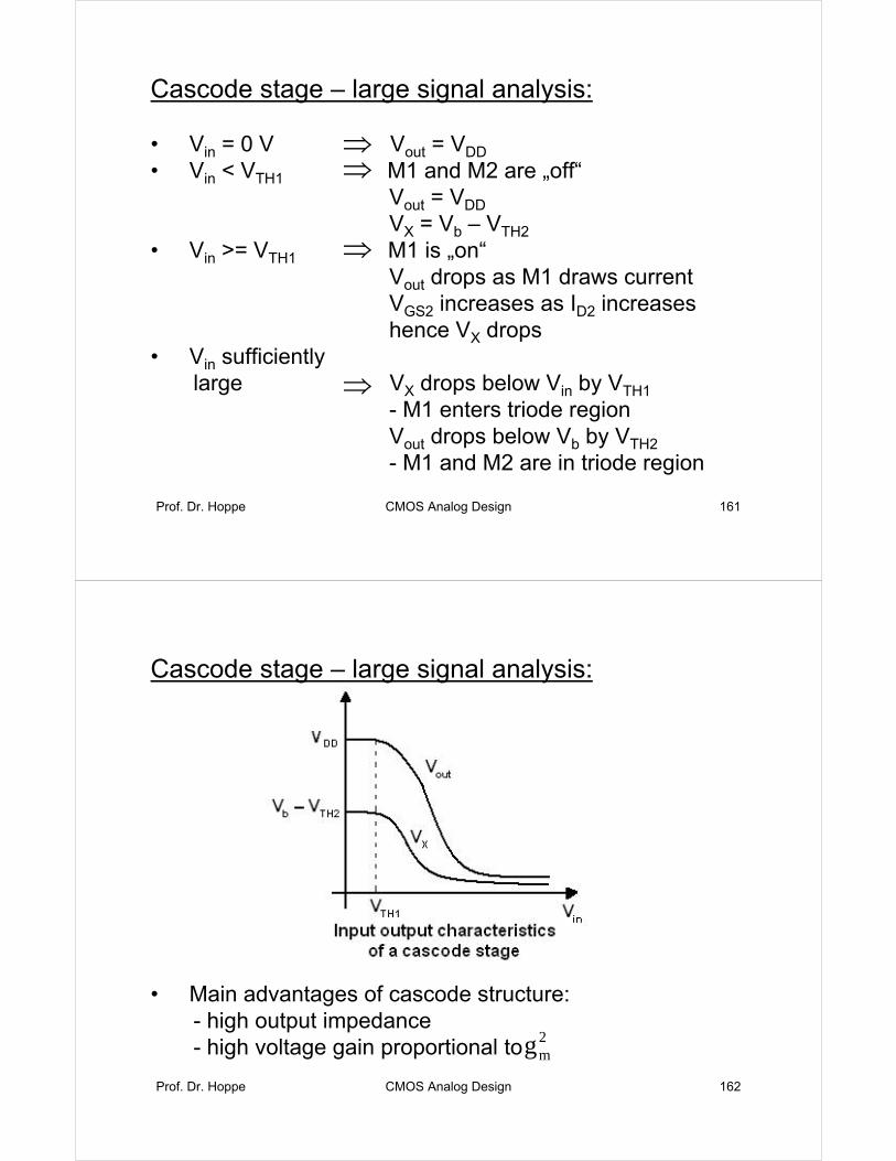
Cascode stage – large signal analysis:
• Vin = 0 V Vout = VDD
• Vin < VTH1 M1 and M2 are „off“Vout = VDD
VX = Vb – VTH2
• Vin >= VTH1 M1 is „on“Vout drops as M1 draws currentVGS2 increases as ID2 increaseshence VX drops
• Vin sufficientlylarge VX drops below Vin by VTH1
- M1 enters triode regionVout drops below Vb by VTH2
- M1 and M2 are in triode region
⇒⇒
⇒
⇒
Prof. Dr. Hoppe CMOS Analog Design 162
Cascode stage – large signal analysis:
• Main advantages of cascode structure: - high output impedance- high voltage gain proportional to
2mg
Prof. Dr. Hoppe CMOS Analog Design 163
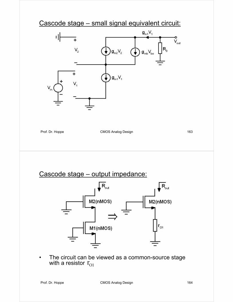
Cascode stage – small signal equivalent circuit:
Prof. Dr. Hoppe CMOS Analog Design 164
Cascode stage – output impedance:
• The circuit can be viewed as a common-source stage with a resistor 1Or
Prof. Dr. Hoppe CMOS Analog Design 165
Cascode stage – output impedance:
• Using the equation of output resistance for common source stage,
• Assuming , we have
• M2 boosts the output impedance of M1 by a factor of !!
( )( ) 2O1O2O2mb2mout rrrgg1R +++=
1rg Om >>( ) 1O2O2mb2mout rrggR +≈
( ) 2O2mb2m rgg +
Prof. Dr. Hoppe CMOS Analog Design 166
Cascode stage – voltage gain:
• Voltage gain of a cascode stage is given as:
• The maximum voltage gain is roughly equal to the square of the intrinsic gain of the transistors
• High output impedance of the cascode stage results in a high voltage gain !
( ) 1O2O2mb2m1m rrgggA +=ν
Prof. Dr. Hoppe CMOS Analog Design 167
Current sources
Prof. Dr. Hoppe CMOS Analog Design 168
Practical current source:
• For an ideal current source and Iout is constant for all output voltages
• Normally is finite and Iout = f(Vout)
∞=Or
Or
Prof. Dr. Hoppe CMOS Analog Design 169
Requirements of a good performance current mirror:
• The current-ratio is precisely set by the aspect-ratio (W/L) and is independent of temperature
• Output impedance is very high, i.e., very high Rout and very low Cout. As a result, the output current is independent of output voltage (DC and AC)
• Input resistance Rin is very low• The voltage compliance is low, i.e., the minimum output
voltage Vout, for which the output acts as a current source, is low
Prof. Dr. Hoppe CMOS Analog Design 170
Basic current mirror:
• M1 is diode connected transistor which is always in saturation
• ID1 is mirrored into transistor M2
Prof. Dr. Hoppe CMOS Analog Design 171
Basic current mirror:
• Since VGS1 = VGS2 and if
provided the channel length modulation effects are very small
•
• Since VGS1 = VGS2 , W/L ratios determine ID2 !
2D1D2
2
1
1 IIL
W
L
W=⇒=
( )2TH1GS1
1oxn1D VV
L
WC
2
1I −µ=
( )2TH2GS2
2oxn2D VV
L
WC
2
1I −µ=
21
12
1D
2D
LW
LW
I
I=
Prof. Dr. Hoppe CMOS Analog Design 172
Basic current mirror:
• OR
where
• What is the minimum voltage across M2 such that M2 remains in saturation?-
• What is the output resistance?where λ is channel
- length modulation factor
( )( ) REF
1
2out I
LW
LWI =
D
SSGSDD1DREF R
VVVII
−−==
2DSTH2GSminout VVVVV =−==
2Dout2m2O I
1
I
1
g
1r
λ=
λ==
Prof. Dr. Hoppe CMOS Analog Design 173
Basic current mirror – design example:
• 5 design variables: L1, W1, L2, W2, and R = f(VGS)
• If we test 10 values per design parameter per simuation, then we need 105 simulations !
• Strategy:step (1): Select a common channel length such that λ is very small
L1 = L2 = L
λ = f(L) should be as small as possibletherefore L >> Lmin
Note: For AMS CSD Lanalog = 1 µm
2
1
2D
1D
W
W
I
I=⇒
Prof. Dr. Hoppe CMOS Analog Design 174
Basic current mirror – design example:
• step (2): Select VGS
VGS is chosen close to VTH in order to have reasonable currents in large devices
VGS – VTH = ∆V is „overdrive“ or excess voltage
60175
λ (1/V) for L = 1µm0.060.06
0.420.58
VTH (V)-0.650.5
Parameterp-channel devicen-channel device
( )2ox VAC21 µµ
( )Vγ
Prof. Dr. Hoppe CMOS Analog Design 175
Basic current mirror – design example:
• For a reasonable overdrive voltage say, ∆V = 0.2V, we get VGS = VTH + ∆V = 0.7 V
• step (3): Calculate R
For example: to design a current mirror ID1 = ID2 = 10 µA the required R can be calculated as
1D
SSGSDD
I
VVVR
−−=
Ω=µ
=µ
−−= k260
A10
6.2
A10
07.03.3R
Prof. Dr. Hoppe CMOS Analog Design 176
Basic current mirror – design example:
• How to implement R = 260 kΩ ?sheet resistance: N-well: 1 kΩ per square
NDIFF: 180 Ω per squarePDIFF: 160 Ω per square
Note: On-chip resistance of such a high value is not possible to implement. To overcome this we usually use externally connected resistances to the IC pins
• step (4): Calculate W1 and W2
( ) A10m1
W*V04.0*
V
A
2
175 122
µ=µ
⎟⎠⎞
⎜⎝⎛ µ∴
( ) A105.07.0*V
AC
L
W
2
1I 2
2oxn1
11D µ=−⎟
⎠⎞
⎜⎝⎛ µµ=
Prof. Dr. Hoppe CMOS Analog Design 177
Basic current mirror – design example:
• step (5): Calculate Vmin
Note: Thus, the minimum output voltage = overdrive voltage selected by the designer
• step (6): Calculate rout
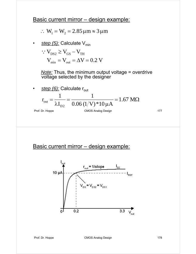
m3m85.2WW 21 µ≈µ==∴
THGS2DS VVV −≥Q
V2.0VVV outmin =∆==
Ω=µ
=λ
= M67.1A10*)V1(06.0
1
I
1r
2Dout
Prof. Dr. Hoppe CMOS Analog Design 178
Basic current mirror – design example:
Prof. Dr. Hoppe CMOS Analog Design 179
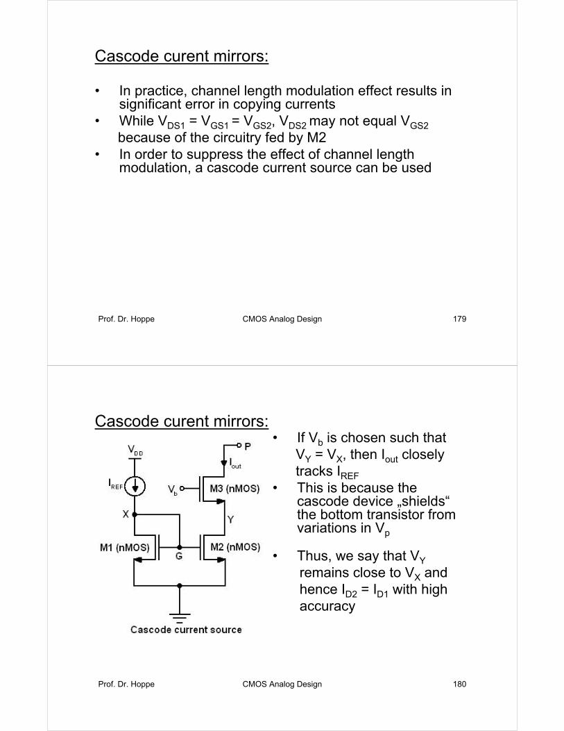
Cascode curent mirrors:
• In practice, channel length modulation effect results in significant error in copying currents
• While VDS1 = VGS1 = VGS2, VDS2 may not equal VGS2
because of the circuitry fed by M2• In order to suppress the effect of channel length
modulation, a cascode current source can be used
Prof. Dr. Hoppe CMOS Analog Design 180
Cascode curent mirrors:• If Vb is chosen such that
VY = VX, then Iout closely tracks IREF
• This is because the cascode device „shields“ the bottom transistor from variations in Vp
• Thus, we say that VY
remains close to VX and hence ID2 = ID1 with high accuracy
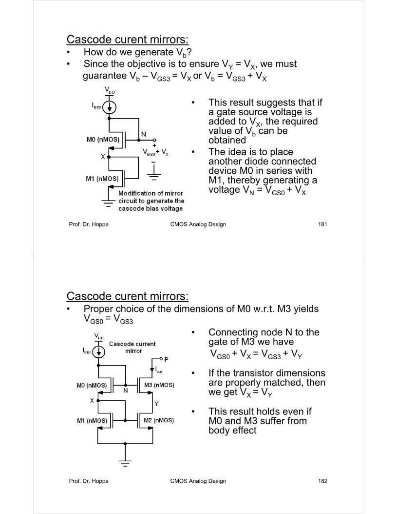
Prof. Dr. Hoppe CMOS Analog Design 181
Cascode curent mirrors:• How do we generate Vb?• Since the objective is to ensure VY = VX, we must
guarantee Vb – VGS3 = VX or Vb = VGS3 + VX
• This result suggests that if a gate source voltage is added to VX, the required value of Vb can be obtained
• The idea is to place another diode connected device M0 in series with M1, thereby generating a voltage VN = VGS0 + VX
Prof. Dr. Hoppe CMOS Analog Design 182
Cascode curent mirrors:• Proper choice of the dimensions of M0 w.r.t. M3 yields
VGS0 = VGS3
• Connecting node N to the gate of M3 we have VGS0 + VX = VGS3 + VY
• If the transistor dimensions are properly matched, then we get VX = VY
• This result holds even if M0 and M3 suffer from body effect