class b data communications network interface … · sae j1850 reaffirmed jun2006-4-1. scope—this...
TRANSCRIPT

SAE Technical Standards Board Rules provide that: “This report is published by SAE to advance the state of technical and engineering sciences. The use of this report is entirelyvoluntary, and its applicability and suitability for any particular use, including any patent infringement arising therefrom, is the sole responsibility of the user.”
SAE reviews each technical report at least every five years at which time it may be reaffirmed, revised, or cancelled. SAE invites your written comments and suggestions.
Copyright © 2006 SAE InternationalAll rights reserved. No part of this publication may be reproduced, stored in a retrieval system or transmitted, in any form or by any means, electronic, mechanical, photocopying,recording, or otherwise, without the prior written permission of SAE.
TO PLACE A DOCUMENT ORDER: Tel: 877-606-7323 (inside USA and Canada)Tel: 724-776-4970 (outside USA)Fax: 724-776-0790Email: [email protected]
SAE WEB ADDRESS: http://www.sae.org
SURFACEVEHICLESTANDARD
J1850REAF.
JUN2006
Issued 1988-11Reaffirmed 2006-06
Superseding J1850 MAY2001
Class B Data Communications Network Interface
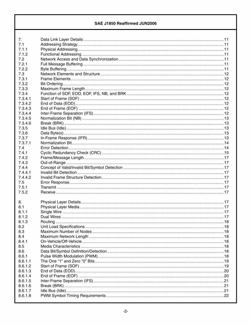
TABLE OF CONTENTS
1. Scope ...................................................................................................................................................... 41.1 Objectives................................................................................................................................................. 41.2 Rationale .................................................................................................................................................. 4
2. References ............................................................................................................................................... 42.1 Applicable Documents.............................................................................................................................. 42.1.1 SAE Publications ...................................................................................................................................... 42.1.2 CISPR Publication .................................................................................................................................... 52.1.3 ISO Publications ....................................................................................................................................... 52.2 Related Publication................................................................................................................................... 52.2.1 SAE Publication........................................................................................................................................ 5
3. Definitions................................................................................................................................................. 5
4. Abbreviations/Acronyms .......................................................................................................................... 6
5. Description of the Architecture ................................................................................................................. 75.1 General..................................................................................................................................................... 75.2 Network Topology ..................................................................................................................................... 75.2.1 Data Bus Topology ................................................................................................................................... 75.2.2 Data Bus Control ...................................................................................................................................... 75.3 References to the OSI Model ................................................................................................................... 75.3.1 Application Layer ...................................................................................................................................... 85.3.2 Data Link Layer ........................................................................................................................................ 95.3.3 Physical Layer .......................................................................................................................................... 95.4 Network Implementation........................................................................................................................... 9
6. Application Layer Details ........................................................................................................................ 106.1 Normal Vehicle Operation (Down the Road) Messages ......................................................................... 106.2 Diagnostic Messages ............................................................................................................................. 106.2.1 Diagnostic Parametric Data .................................................................................................................... 106.2.2 Diagnostic Malfunction Codes ................................................................................................................ 116.3 Frame Filtering ....................................................................................................................................... 11
SAE J1850 Reaffirmed JUN2006
-2-
7. Data Link Layer Details ...........................................................................................................................117.1 Addressing Strategy................................................................................................................................117.1.1 Physical Addressing................................................................................................................................117.1.2 Functional Addressing ............................................................................................................................117.2 Network Access and Data Synchronization ............................................................................................117.2.1 Full Message Buffering ...........................................................................................................................117.2.2 Byte Buffering .........................................................................................................................................117.3 Network Elements and Structure ............................................................................................................127.3.1 Frame Elements......................................................................................................................................127.3.2 Bit Ordering.............................................................................................................................................127.3.3 Maximum Frame Length .........................................................................................................................127.3.4 Function of SOF, EOD, EOF, IFS, NB, and BRK .....................................................................................127.3.4.1 Start of Frame (SOF) ..............................................................................................................................127.3.4.2 End of Data (EOD)..................................................................................................................................127.3.4.3 End of Frame (EOF) ...............................................................................................................................127.3.4.4 Inter-Frame Separation (IFS) ..................................................................................................................127.3.4.5 Normalization Bit (NB) ............................................................................................................................137.3.4.6 Break (BRK)............................................................................................................................................137.3.5 Idle Bus (Idle)..........................................................................................................................................137.3.6 Data Byte(s) ............................................................................................................................................137.3.7 In-Frame Response (IFR) .......................................................................................................................137.3.7.1 Normalization Bit.....................................................................................................................................147.4 Error Detection........................................................................................................................................147.4.1 Cyclic Redundancy Check (CRC) ...........................................................................................................157.4.2 Frame/Message Length ..........................................................................................................................177.4.3 Out-of-Range ..........................................................................................................................................177.4.4 Concept of Valid/Invalid Bit/Symbol Detection ........................................................................................177.4.4.1 Invalid Bit Detection ................................................................................................................................177.4.4.2 Invalid Frame Structure Detection...........................................................................................................177.5 Error Response.......................................................................................................................................177.5.1 Transmit ..................................................................................................................................................177.5.2 Receive ...................................................................................................................................................17
8. Physical Layer Details.............................................................................................................................178.1 Physical Layer Media ..............................................................................................................................178.1.1 Single Wire .............................................................................................................................................178.1.2 Dual Wires ..............................................................................................................................................178.1.3 Routing ...................................................................................................................................................188.2 Unit Load Specifications .........................................................................................................................188.3 Maximum Number of Nodes ...................................................................................................................188.4 Maximum Network Length ......................................................................................................................188.4.1 On-Vehicle/Off-Vehicle ............................................................................................................................188.5 Media Characteristics .............................................................................................................................188.6 Data Bit/Symbol Definition/Detection ......................................................................................................188.6.1 Pulse Width Modulation (PWM) ..............................................................................................................188.6.1.1 The One “1” and Zero “0” Bits.................................................................................................................198.6.1.2 Start of Frame (SOF) ..............................................................................................................................198.6.1.3 End of Data (EOD)..................................................................................................................................208.6.1.4 End of Frame (EOF) ...............................................................................................................................208.6.1.5 Inter-Frame Separation (IFS) ..................................................................................................................218.6.1.6 Break (BRK)............................................................................................................................................218.6.1.7 Idle Bus (Idle)..........................................................................................................................................218.6.1.8 PWM Symbol Timing Requirements .......................................................................................................22
SAE J1850 Reaffirmed JUN2006
-3-
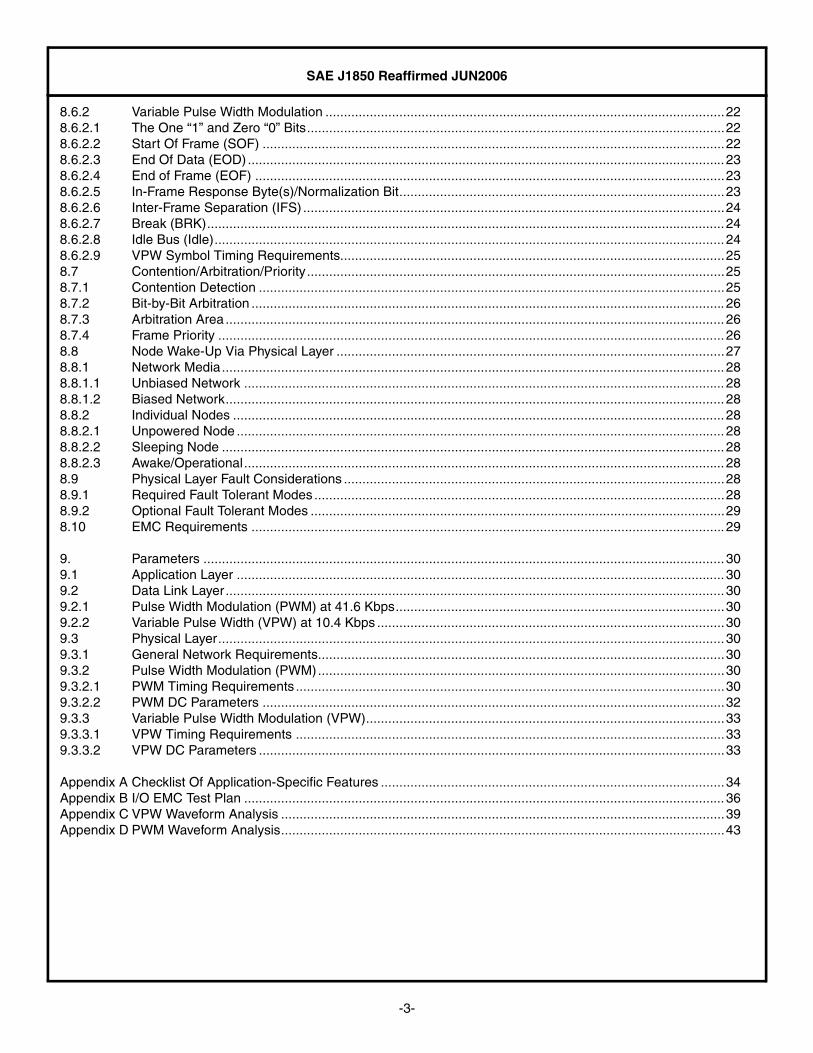
8.6.2 Variable Pulse Width Modulation ............................................................................................................228.6.2.1 The One “1” and Zero “0” Bits.................................................................................................................228.6.2.2 Start Of Frame (SOF) .............................................................................................................................228.6.2.3 End Of Data (EOD) .................................................................................................................................238.6.2.4 End of Frame (EOF) ...............................................................................................................................238.6.2.5 In-Frame Response Byte(s)/Normalization Bit........................................................................................238.6.2.6 Inter-Frame Separation (IFS) ..................................................................................................................248.6.2.7 Break (BRK)............................................................................................................................................248.6.2.8 Idle Bus (Idle)..........................................................................................................................................248.6.2.9 VPW Symbol Timing Requirements........................................................................................................258.7 Contention/Arbitration/Priority .................................................................................................................258.7.1 Contention Detection ..............................................................................................................................258.7.2 Bit-by-Bit Arbitration ................................................................................................................................268.7.3 Arbitration Area .......................................................................................................................................268.7.4 Frame Priority .........................................................................................................................................268.8 Node Wake-Up Via Physical Layer .........................................................................................................278.8.1 Network Media ........................................................................................................................................288.8.1.1 Unbiased Network ..................................................................................................................................288.8.1.2 Biased Network.......................................................................................................................................288.8.2 Individual Nodes .....................................................................................................................................288.8.2.1 Unpowered Node ....................................................................................................................................288.8.2.2 Sleeping Node ........................................................................................................................................288.8.2.3 Awake/Operational..................................................................................................................................288.9 Physical Layer Fault Considerations .......................................................................................................288.9.1 Required Fault Tolerant Modes ...............................................................................................................288.9.2 Optional Fault Tolerant Modes ................................................................................................................298.10 EMC Requirements ................................................................................................................................29
9. Parameters .............................................................................................................................................309.1 Application Layer ....................................................................................................................................309.2 Data Link Layer .......................................................................................................................................309.2.1 Pulse Width Modulation (PWM) at 41.6 Kbps.........................................................................................309.2.2 Variable Pulse Width (VPW) at 10.4 Kbps ..............................................................................................309.3 Physical Layer.........................................................................................................................................309.3.1 General Network Requirements..............................................................................................................309.3.2 Pulse Width Modulation (PWM) ..............................................................................................................309.3.2.1 PWM Timing Requirements ....................................................................................................................309.3.2.2 PWM DC Parameters .............................................................................................................................329.3.3 Variable Pulse Width Modulation (VPW).................................................................................................339.3.3.1 VPW Timing Requirements ....................................................................................................................339.3.3.2 VPW DC Parameters ..............................................................................................................................33
Appendix A Checklist Of Application-Specific Features .............................................................................................34Appendix B I/O EMC Test Plan ..................................................................................................................................36Appendix C VPW Waveform Analysis ........................................................................................................................39Appendix D PWM Waveform Analysis........................................................................................................................43
SAE J1850 Reaffirmed JUN2006
-4-
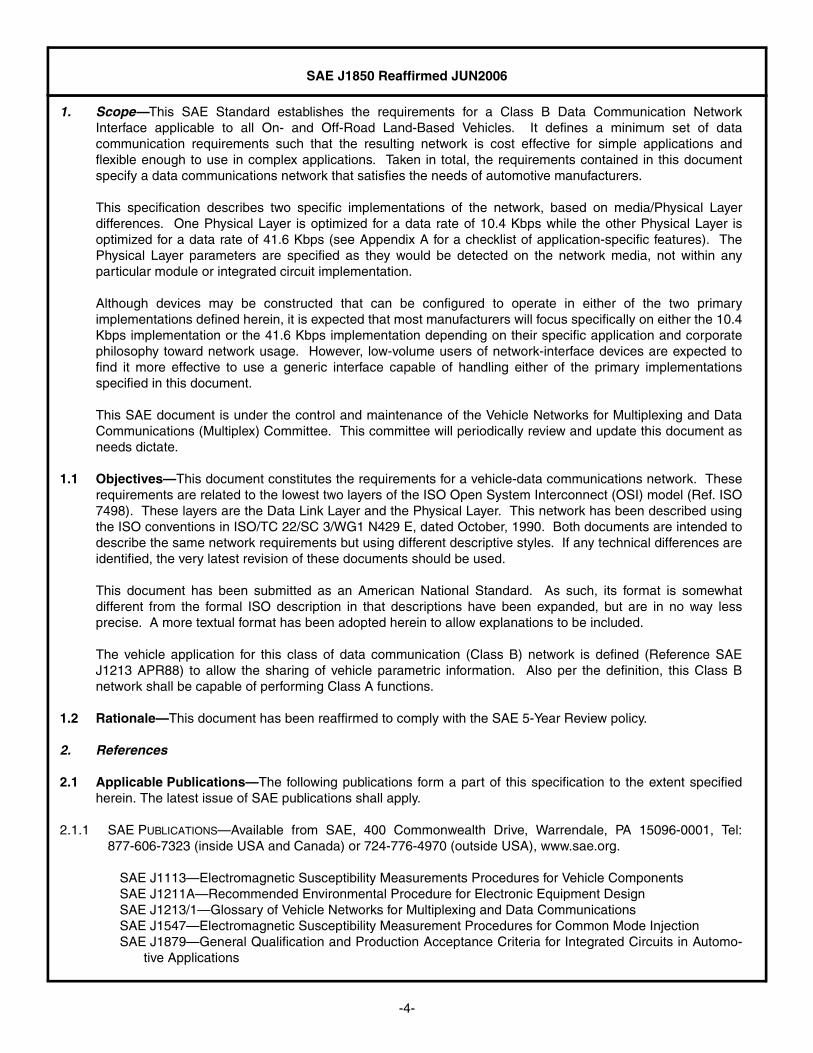
1. Scope—This SAE Standard establishes the requirements for a Class B Data Communication NetworkInterface applicable to all On- and Off-Road Land-Based Vehicles. It defines a minimum set of datacommunication requirements such that the resulting network is cost effective for simple applications andflexible enough to use in complex applications. Taken in total, the requirements contained in this documentspecify a data communications network that satisfies the needs of automotive manufacturers.
This specification describes two specific implementations of the network, based on media/Physical Layerdifferences. One Physical Layer is optimized for a data rate of 10.4 Kbps while the other Physical Layer isoptimized for a data rate of 41.6 Kbps (see Appendix A for a checklist of application-specific features). ThePhysical Layer parameters are specified as they would be detected on the network media, not within anyparticular module or integrated circuit implementation.
Although devices may be constructed that can be configured to operate in either of the two primaryimplementations defined herein, it is expected that most manufacturers will focus specifically on either the 10.4Kbps implementation or the 41.6 Kbps implementation depending on their specific application and corporatephilosophy toward network usage. However, low-volume users of network-interface devices are expected tofind it more effective to use a generic interface capable of handling either of the primary implementationsspecified in this document.
This SAE document is under the control and maintenance of the Vehicle Networks for Multiplexing and DataCommunications (Multiplex) Committee. This committee will periodically review and update this document asneeds dictate.
1.1 Objectives—This document constitutes the requirements for a vehicle-data communications network. Theserequirements are related to the lowest two layers of the ISO Open System Interconnect (OSI) model (Ref. ISO7498). These layers are the Data Link Layer and the Physical Layer. This network has been described usingthe ISO conventions in ISO/TC 22/SC 3/WG1 N429 E, dated October, 1990. Both documents are intended todescribe the same network requirements but using different descriptive styles. If any technical differences areidentified, the very latest revision of these documents should be used.
This document has been submitted as an American National Standard. As such, its format is somewhatdifferent from the formal ISO description in that descriptions have been expanded, but are in no way lessprecise. A more textual format has been adopted herein to allow explanations to be included.
The vehicle application for this class of data communication (Class B) network is defined (Reference SAEJ1213 APR88) to allow the sharing of vehicle parametric information. Also per the definition, this Class Bnetwork shall be capable of performing Class A functions.
1.2 Rationale—This document has been reaffirmed to comply with the SAE 5-Year Review policy.
2. References
2.1 Applicable Publications—The following publications form a part of this specification to the extent specifiedherein. The latest issue of SAE publications shall apply.
2.1.1 SAE PUBLICATIONS—Available from SAE, 400 Commonwealth Drive, Warrendale, PA 15096-0001, Tel:877-606-7323 (inside USA and Canada) or 724-776-4970 (outside USA), www.sae.org.
SAE J1113—Electromagnetic Susceptibility Measurements Procedures for Vehicle ComponentsSAE J1211A—Recommended Environmental Procedure for Electronic Equipment DesignSAE J1213/1—Glossary of Vehicle Networks for Multiplexing and Data CommunicationsSAE J1547—Electromagnetic Susceptibility Measurement Procedures for Common Mode InjectionSAE J1879—General Qualification and Production Acceptance Criteria for Integrated Circuits in Automo-
tive Applications

SAE J1850 Reaffirmed JUN2006
-5-
SAE J1962—Diagnostic ConnectorSAE J1979—E/E Diagnostic Test ModesSAE J2012—Diagnostic Codes/MessagesSAE J2178—Class B Data Communication Network MessagesSAE J2178/1—Class B Data Communication Network Messages: Detailed Header Formats and Physical
Address AssignmentSAE J2190—Enhanced E/E Diagnostic Test Modes
2.1.2 CISPR PUBLICATION—Electronic copy available from ANSI, 25 West 43rd Street, New York, NY 10036-8002,Tel: 1-888-267-4783, email: [email protected].
CISPR/D/WG2 (Secretariat) 19 Sept 1989—Radiated Emissions Antenna and Probe Test
2.1.3 ISO PUBLICATIONS—Available from ANSI, 25 West 43rd Street, New York, NY 10036-8002, Tel:212-642-4900, www.ansi.org.
ISO/TC22/SC3/WG1 N429E OCT90—Road vehicles—Serial data communication for automotiveapplications, low speed (125 Kbps and below)
ISO 7498—Data processing systems—Open systems interconnection—Standard reference modelISO 7637/3—Road vehicles—Electrical disturbance by conduction and coupling—Part 3: Passenger cars
and light commercial vehicles with nominal 12 V supply voltage and commercial vehicles with 24 Vsupply voltage—Electrical transient transmission by capacitive and inductive coupling via lines otherthan supply lines
2.2 Related Publications—The following publication is provided for information purposes only and is not arequired part of this document.
2.2.1 SAE PUBLICATION—Available from SAE, 400 Commonwealth Drive, Warrendale, PA 15096-0001, Tel:877-606-7323 (inside USA and Canada) or 724-776-4970 (outside USA), www.sae.org.
SAE J1930—Electrical/Electronic Systems Diagnostic Terms, Definitions, Abbreviations, & Acronyms
3. Definitions
3.1 Active State—The state of a bus wire which results when one or more nodes have “turned on” their physicallayer circuitry. This is Voh volts for Bus + (PWM and VPW) and Vol volts for Bus – (PWM only). Refer to 9.3.2.2(PWM DC Parameters) and 9.3.3.2 (VPW DC Parameters) for the values of Voh and Vol. The active statevoltage level is determined by the source voltage of the physical layer drive circuitry.
3.2 Arbitration—The process of resolving which frame, or In-Frame Response data, continues to be transmittedwhen two or more nodes begin transmitting frames, or In-Frame Response data, simultaneously.
3.3 Class A Data Communications—A system whereby vehicle wiring is reduced by the transmission andreception of multiple signals over the same signal bus between nodes that would have been accomplished byindividual wires in a conventionally wired vehicle. The nodes used to accomplish multiplexed body wiringtypically did not exist in the same or similar form in a conventionally wired vehicle.
3.4 Class B Data Communications—A system whereby data (e.g., parametric data values) is transferredbetween nodes to eliminate redundant sensors and other system elements. The nodes in this form of amultiplex system typically already existed as stand-alone modules in a conventionally wired vehicle. A Class Bnetwork shall also be capable of performing Class A functions.
SAE J1850 Reaffirmed JUN2006
-6-
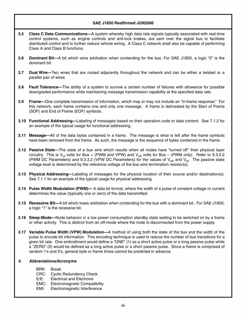
3.5 Class C Data Communications—A system whereby high data rate signals typically associated with real-timecontrol systems, such as engine controls and anti-lock brakes, are sent over the signal bus to facilitatedistributed control and to further reduce vehicle wiring. A Class C network shall also be capable of performingClass A and Class B functions.
3.6 Dominant Bit—A bit which wins arbitration when contending for the bus. For SAE J1850, a logic “0” is thedominant bit.
3.7 Dual Wire—Two wires that are routed adjacently throughout the network and can be either a twisted or aparallel pair of wires.
3.8 Fault Tolerance—The ability of a system to survive a certain number of failures with allowance for possibledowngraded performance while maintaining message transmission capability at the specified data rate.
3.9 Frame—One complete transmission of information, which may or may not include an “in-frame response.” Forthis network, each frame contains one and only one message. A frame is delineated by the Start of Frame(SOF) and End of Frame (EOF) symbols.
3.10 Functional Addressing—Labeling of messages based on their operation code or data content. See 7.1.2 foran example of the typical usage for functional addressing.
3.11 Message—All of the data bytes contained in a frame. The message is what is left after the frame symbolshave been removed from the frame. As such, the message is the sequence of bytes contained in the frame.
3.12 Passive State—The state of a bus wire which results when all nodes have “turned off” their physical layercircuitry. This is Vol volts for Bus + (PWM and VPW) and Voh volts for Bus – (PWM only). Refer to 9.3.2.2(PWM DC Parameters) and 9.3.3.2 (VPW DC Parameters) for the values of Voh and Vol. The passive statevoltage level is determined by the reference voltage of the bus wire termination resistor(s).
3.13 Physical Addressing—Labeling of messages for the physical location of their source and/or destination(s).See 7.1.1 for an example of the typical usage for physical addressing.
3.14 Pulse Width Modulation (PWM)— A data bit format, where the width of a pulse of constant voltage or currentdetermines the value (typically one or zero) of the data transmitted.
3.15 Recessive Bit—A bit which loses arbitration when contending for the bus with a dominant bit. For SAE J1850,a logic “1” is the recessive bit.
3.16 Sleep-Mode—Node behavior in a low power consumption standby state waiting to be switched on by a frameor other activity. This is distinct from an off-mode where the node is disconnected from the power supply.
3.17 Variable Pulse Width (VPW) Modulation—A method of using both the state of the bus and the width of thepulse to encode bit information. This encoding technique is used to reduce the number of bus transitions for agiven bit rate. One embodiment would define a “ONE” (1) as a short active pulse or a long passive pulse whilea “ZERO” (0) would be defined as a long active pulse or a short passive pulse. Since a frame is comprised ofrandom 1's and 0's, general byte or frame times cannot be predicted in advance.
4. Abbreviations/Acronyms
BRK: BreakCRC: Cyclic Redundancy CheckE/E: Electrical and ElectronicEMC: Electromagnetic CompatibilityEMI: Electromagnetic Interference
SAE J1850 Reaffirmed JUN2006
-7-
EOD: End of DataEOF: End of FrameIFR: In-Frame Response (Byte/Bytes)IFS: Inter-Frame SeparationISO: International Standards OrganizationKbps: Kilo bits per secondNA: Not ApplicableNB: Normalization BitOSI: Open System InterconnectSOF: Start of Frame
5. Description of the Architecture
5.1 General—It is the intent of this network to interconnect different electronic modules on the vehicle using an“Open Architecture” approach. An open architecture network is one in which the addition or deletion of one ormore modules (data nodes) has minimal hardware and/or software impact on the remaining modules.
In order to support an open architecture approach, the Class B network utilizes the concept of Carrier SenseMultiple Access (CSMA) with nondestructive contention resolution. Additionally this network supports theprioritization of frames such that, in the case of contention, the higher priority frames will always win arbitrationand be completed.
5.2 Network Topology
5.2.1 DATA BUS TOPOLOGY—Data bus topology is the map of physical connections of the data bus nodes to thedata bus. It includes all nodes and data buses involved in the data bus integration of the vehicle. A single-level bus topology, the simplest bus topology, is currently being used in several automotive applications. In asingle-level bus topology, all nodes are interconnected via the same data bus. The redundancy requirementsof a particular application may require a single-level topology to be implemented using multipleinterconnecting cables operating in various modes (active or passive). However, the requirement to usemultiple buses for redundancy purposes does not change the single-level bus topology definition if thefollowing criteria are maintained:
a. All nodes/devices transmit and receive from a single path.b. All nodes/devices receive all frames at the same time.c. Communication on each data bus is identical.
5.2.2 DATA BUS CONTROL—Although various methods of data bus control can be used, this Class B network isintended for “masterless” bus control. The principal advantage of the masterless bus control concept is itsability to provide the basis for an open-architecture data communications system. Since a master does notexist, each node has an equal opportunity to initiate a data transmission once an idle bus has been detected.However, not all nodes and/or data are of equal importance, prioritization of frames is allowed and thehighest priority frame will always be completed. This also implies that frame/data contention will not result inlost data. Two disadvantages of the masterless bus concept are that data latency cannot be guaranteed,except for the single highest system priority frame, and bus utilization extremes are difficult to evaluate.
5.3 References to the OSI Model—Although this document focuses on the data link layer and the physical layer,references are included for the application layer since this needs to be included for emission-related, diagnosticcommunication legislation requirements. The Class B network maps into the OSI model as described in thefollowing paragraphs. This “mapping” is illustrated in Figure 1.
SAE J1850 Reaffirmed JUN2006
-8-
FIGURE 1—MAP OF SAE J1850 TO THE ISO OSI MODEL
5.3.1 APPLICATION LAYER—At the top of the OSI reference model is the Application Layer. This layer establishesthe relationship between the various application input and output devices, including what is expected ofhuman operators. This layer documents the high level description of the function including control algorithmsif appropriate. An example of an Application Layer functional description might be: “Pressing the head lampbutton shall cause the low beam head lamp, marker and tail lamp filaments to be energized.” Legislateddiagnostics is another area in which application layer requirements need to be specified.

SAE J1850 Reaffirmed JUN2006
-9-
5.3.2 DATA LINK LAYER—The primary function of the Data Link Layer is to convert bits and/or symbols to validatederror free frames/data. Typical services provided are serialization (parallel to serial conversion) and clockrecovery or bit synchronization. An important additional service provided by the Data Link Layer is errorchecking. When errors are detected, they may be corrected or higher layers may be notified.
5.3.3 PHYSICAL LAYER—The Physical Layer and its associated wiring form the interconnecting path for informationtransfer between Data Link Layers. Typical Physical Layer protocol elements include voltage/current levels,media impedance, and bit/symbol definition and timing.
5.4 Network Implementation—The network implementations based on this document have been reduced tocommonize hardware, software, messages, and tools. The consolidation of messages has been documentedin SAE J2178. The first byte or the first three bytes of these messages are called the “Header” byte(s). Theseheader bytes fully define the associated requirements of this network interface, which previously had beenoptional. Figure 2 shows the general format for single byte header forms. Figure 3 shows the three byteheader form. Figure 4 shows the specific bit assignments for priority, In-Frame Response, and Functional/Physical Address mapping in the three byte header format. For a complete description of the “KYZZ” bitsshown in Figure 4 refer to SAE J2178/1.
FIGURE 2—SINGLE BYTE HEADER AND ONE BYTE FORM OF CONSOLIDATED HEADER
FIGURE 3—THREE BYTE FORM OF CONSOLIDATED HEADER
SAE J1850 Reaffirmed JUN2006
-10-
FIGURE 4—FIRST BYTE OF THREE BYTE FORM OF CONSOLIDATED HEADER
6. Application Layer Details—The application of this communication network is the transfer of information fromone node of the network to one or more other nodes. This transfer of information supports both operationaland diagnostic needs. SAE has developed documents describing each of these types of applications,consistent with this document.
6.1 Normal Vehicle Operation (Down the Road) Messages—The messages sent during non-diagnosticoperations are called normal vehicle operation messages. These normal vehicle operation messages areused for communication from a transmitter to one or more receivers across this network. The normal operationmessages have been developed by the SAE for this communication network and are defined in SAE J2178.SAE defined messages and the “Reserved” messages of SAE J2178 shall remain specific to those definitions.In SAE J2178, there is also a set of “Reserved - Manufacturer” messages which, if used, will have meaningsspecific to a vehicle manufacturer but are likely to be different between manufacturers.
6.2 Diagnostic Messages—It is expected that this network will be used for diagnostics of the devices utilizing thenetwork. These diagnostic procedures may include legislated diagnostics, industry standard diagnostics, ormanufacturer-specific diagnostic procedures.
Legislated diagnostics, and some level of voluntary industry standard diagnostics that reference this document,should only specify procedures and frames that conform to this document. SAE J1979 and SAE J2190 definethe set of recognized test modes that are available and have been reserved for diagnostic purposes.
Manufacturer-specific test procedures utilizing this network may specify procedures that do not conform to therequirements of this recommended practice.
6.2.1 DIAGNOSTIC PARAMETRIC DATA—SAE J1979 and SAE J2190 define test modes and frame formats for use byoff-vehicle test equipment to obtain diagnostic data from the vehicle. SAE J1979 and SAE J2190 messagesconform to the requirements and limitations of this document.

SAE J1850 Reaffirmed JUN2006
-11-
6.2.2 DIAGNOSTIC MALFUNCTION CODES—SAE J2012 defines trouble codes to be assigned to various vehiclesystem malfunctions, and also assigns ranges of codes to be used for manufacturer-specific codes. SAEJ1979 and SAE J2190 include messages to be used to retrieve these codes from the on-vehicle systems.When trouble codes are to be assigned to system malfunctions, the code structure of SAE J2012 should beused.
6.3 Frame Filtering—The network interface device may be capable of filtering frames on the network to selectthose appropriate to a given node. Because this Class B protocol may use more than one type of frameaddressing (e.g., functional and physical; see 7.1), the criteria for these filtering operations may includemultiple byte comparisons occurring over the first several frame bytes. Regardless of the exact technique usedfor frame filtering, the objective is to reduce the software and processing burden associated with networkoperations by limiting the number of received frames to just those necessary for any given node.
7. Data Link Layer Details—This section defines the requirements on the following Data Link Layer attributes:
a. Addressing Strategyb. Network Access and Data Synchronizationc. Frame Elements and Structured. Error Detectione. Error Response
7.1 Addressing Strategy—Two types of addressing strategies are defined and can co-exist on this network. Thetwo strategies serve different types of tasks and the flexibility to use both types on the same network providesa major benefit.
7.1.1 PHYSICAL ADDRESSING—Frames are exchanged only between two devices based on their “Physical” addresswithin the network. Each node must be assigned a unique physical address within the network. This type ofaddressing strategy is used when the communications involve specific nodes and not the others that may beon the network. Diagnostic access would be one case where identification of a specific module is important.
7.1.2 FUNCTIONAL ADDRESSING—Frames can be transmitted between many devices based on the function of thatframe on the network. Each node is assigned the set of functions that it cares about, either as transmitter orreceiver, and can be located anywhere in the network. This type of addressing strategy is used when thephysical location of the function is not important but could move around from one module to another. In thecase of functional addressing, the function of the message is important and not the physical addresses of thenodes.
7.2 Network Access and Data Synchronization—The network interface shall implement a multiple accessarbitration-based protocol using nondestructive bit-by-bit arbitration to transparently resolve simultaneousaccess to the bus. Network access is allowed after detection of an idle bus. The definition of an idle bus iscontained in 8.6.1.7.
Since a discrete clock wire is not used with this network, node synchronization can be derived from bit/symboltransitions on the bus.
7.2.1 FULL MESSAGE BUFFERING—One or more messages exist in their entirety in the interface device. Thisapproach reduces software burden at the expense of hardware costs. Message filtering (or screening) ispossible in such a device which reduces software burden even further.
7.2.2 BYTE BUFFERING—Each byte of a received message (or transmit message) is stored individually in theinterface device. The controlling device is responsible for the timely servicing of the interface device to keepup with frame traffic.

SAE J1850 Reaffirmed JUN2006
-12-
7.3 Network Elements and Structure—The general format is:
idle, SOF, DATA_0, ..., DATA_N, CRC, EOD, NB, IFR_1, ..., IFR_N, EOF, IFS, idle:
The preceding acronyms are defined as follows:
idle: Idle Bus (occurs before SOF and after IFS)SOF: Start of FrameDATA: Data bytes (each 8 bits long)EOD: End of Data (only when IFR is used)CRC: CRC Error Detection Byte (may occur in IFR as well)NB: Normalization Bit (10.4 Kbps only)IFR: In-Frame Response Byte(s)EOF: End of FrameIFS: Inter-Frame Separation
NOTE—Break (BRK) can occur (be sent) on a network at any time.
7.3.1 FRAME ELEMENTS—The frame elements other than the symbols SOF, EOD, NB, EOF, IFS, and BRK will bebyte oriented and must end on byte boundaries. Each byte will be 8 bits in length.
7.3.2 BIT ORDERING—The first bit of each byte transmitted on the network shall be the most significant bit (i.e.,MSB first).
7.3.3 MAXIMUM FRAME LENGTH—The maximum number of continuous bit times that a single node is able to controlthe bus shall not exceed the value specified in 9.2.
7.3.4 FUNCTION OF SOF, EOD, EOF, IFS, NB, AND BRK—In addition to actual data bytes (i.e., data, CRC, IFR)frame delimiter symbols are defined to allow the data bus to function properly in a multitude of differentapplications. An overview of these symbols is provided here. Detailed timing requirements on each symbolcan be found in 9.3.
7.3.4.1 Start of Frame (SOF)—The SOF mark is used to uniquely identify the start of a frame. The SOF markshall not be used in the calculation of the CRC error detection code.
7.3.4.2 End of Data (EOD)—End of Data (EOD) is used to signal the end of transmission by the originator of aframe. The in-frame response (IFR) section of the frame, if used, begins after the EOD time but before theEOF. If the IFR feature (see 7.3.7) is not used, then the bus would remain in the passive state therebyresulting in an End of Frame (EOF). If a frame includes an IFR, the originator of the frame will expect therecipient(s) of the frame to drive the network with one or more in-frame response bytes immediatelyfollowing EOD.
7.3.4.3 End of Frame (EOF)—The completion of the EOF defines the end of a frame. After the last transmissionbyte (including in-frame response bytes where applicable), the bus will be left in a passive state. WhenEOF has expired, all receivers will consider the transmission complete.
7.3.4.4 Inter-Frame Separation (IFS)—Inter-Frame Separation is used to allow proper synchronization of variousnodes during back-to-back frame transmissions. A transmitter must not initiate transmission on the busbefore the completion of the IFS minimum period. However, receivers must synchronize to any other SOFoccurring after the EOF minimum period in order to accommodate individual clock tolerances.
SAE J1850 Reaffirmed JUN2006
-13-
A transmitter that desires bus access must wait for either of two conditions before transmitting a SOF:
a. IFS minimum has expired.b. EOF minimum has expired and another rising edge has been detected.
7.3.4.5 Normalization Bit (NB)—Only applicable to 10.4 Kbps implementation. For Variable Pulse WidthModulation, the first bit of In-Frame Response data is also passive and, therefore it is necessary togenerate a Normalization Bit to follow the EOD symbol. This Normalization Bit shall define the start of thein-frame response. The Normalization Bit is defined in 8.6.2.5.
7.3.4.6 Break (BRK)—BRK is allowed to accommodate those situations in which bus communication is to beterminated and all nodes reset to a “ready-to-receive” state. If BRK is used, it must adhere to therequirements as specified in 8.6.
7.3.5 IDLE BUS (IDLE)—Idle bus is defined as any period of passive bus state occurring after IFS. During an idlebus, any node may transmit immediately. Contention may still occur when two or more nodes transmit nearlysimultaneously; therefore, resynchronization to rising edges must continue to occur.
7.3.6 DATA BYTE(S)—A number of data bytes, each eight (8) bits in length, can be transmitted at the discretion ofthe system designer. However, the total message length (from SOF to EOF) shall not exceed the limitdefined in 9.2.
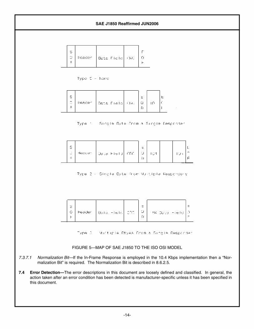
7.3.7 IN-FRAME RESPONSE (IFR)—For In-Frame Response, the response byte(s) are transmitted by the respondersand begin after EOD. If the first bit of the in-frame response byte does not occur at this point and the busremains passive for a period of time defined as EOF, then the originator and all receivers must consider theframe complete. In-frame response bytes may take one of the following forms (refer to Figure 5):
a. Noneb. A single byte transmitted from a single recipient, typically a unique identifier (ID) or address.c. Multiple bytes, a single byte transmitted from each recipient. The effect is to concatenate the individual
response bytes into a response “stream.” The response byte from each recipient must be unique,typically a physical address (ID n). Arbitration takes place during the response process so that eachrecipient, if arbitration is lost during its response byte, will retransmit the single byte until the recipientobserves its unique byte in the response stream. Once a given recipient observes its own uniqueresponse byte, it discontinues the transmission process to allow any remaining responders to transmittheir byte.
d. One or more data bytes, all from a single recipient. A CRC byte may be appended to the data byte(s).The CRC byte is calculated as described in 7.4.1, except only the data in the response is used for theCRC calculation.
Refer to SAE J2178/1 for a detailed discussion of the different IFR types and for determination of whichmessage types utilize which IFR types.
If in-frame response bytes are used, the overall frame/message length limit remains in effect. The sum totalof data bytes, CRC bytes, and in-frame response bytes shall not exceed the frame length as specified in 9.2.
SAE J1850 Reaffirmed JUN2006
-14-
FIGURE 5—MAP OF SAE J1850 TO THE ISO OSI MODEL
7.3.7.1 Normalization Bit—If the In-Frame Response is employed in the 10.4 Kbps implementation then a “Nor-malization Bit” is required. The Normalization Bit is described in 8.6.2.5.
7.4 Error Detection—The error descriptions in this document are loosely defined and classified. In general, theaction taken after an error condition has been detected is manufacturer-specific unless it has been specified inthis document.
SAE J1850 Reaffirmed JUN2006
-15-
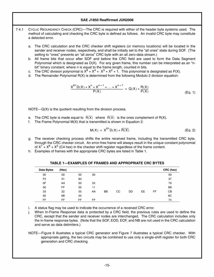
7.4.1 CYCLIC REDUNDANCY CHECK (CRC)—The CRC is required with either of the header byte systems used. Themethod of calculating and checking the CRC byte is defined as follows. An invalid CRC byte may constitutea detected error.
a. The CRC calculation and the CRC checker shift registers (or memory locations) will be located in thesender and receiver nodes, respectively, and shall be initially set to the “all ones” state during SOF. (Thesetting to “ones” prevents an “all zeros” CRC byte with an all zero-data stream.)
b. All frame bits that occur after SOF and before the CRC field are used to form the Data SegmentPolynomial which is designated as D(X). For any given frame, this number can be interpreted as an “n-bit” binary constant, where n is equal to the frame length, counted in bits.
c. The CRC division polynomial is X8 + X4 + X3 + X2 + 1. This polynomial is designated as P(X).d. The Remainder Polynomial R(X) is determined from the following Modulo 2 division equation:
(Eq. 1)
NOTE—Q(X) is the quotient resulting from the division process.
e. The CRC byte is made equal to where is the ones complement of R(X).f. The Frame Polynomial M(X) that is transmitted is shown in Equation 2:
(Eq. 2)
g. The receiver checking process shifts the entire received frame, including the transmitted CRC byte,through the CRC checker circuit. An error-free frame will always result in the unique constant polynomialof X7 + X6 + X2 (C4 hex) in the checker shift register regardless of the frame content.
h. Examples of frames with the appropriate CRC bytes are listed in Table 1.
i. A status flag may be used to indicate the occurrence of a received CRC error.j. When In-Frame Response data is protected by a CRC field, the previous rules are used to define the
CRC, except that the sender and receiver nodes are interchanged. The CRC calculation includes onlythe in-frame response bytes. (Note that the SOF, EOD, EOF, and NB are not used in the CRC calculationand serve as data delimiters.)
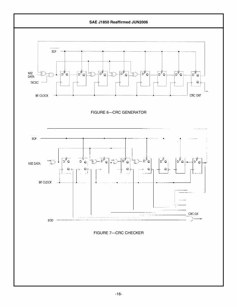
NOTE—Figure 6 illustrates a typical CRC generator and Figure 7 illustrates a typical CRC checker. Withappropriate gating, the two circuits may be combined to use only a single-shift register for both CRCgeneration and CRC checking.
TABLE 1—EXAMPLES OF FRAMES AND APPROPRIATE CRC BYTES
Data Bytes (Hex) CRC (hex)
00 00 00 00 59
F2 01 83 37
0F AA 00 55 79
00 FF 55 11 B8
33 22 55 AA BB CC DD EE FF CB
92 6B 55 8C
FF FF FF FF 74
X8∗D X( ) Xn Xn 1+ … Xn 7++ + + +
P X( )−−−−−−−−−−−−−−−−−−−−−−−−−−−−−−−−−−−−−−−−−−−−−−−−−−−−−− Q X( ) R X( )
P X( )−−−−−−−−+=
R X( ) R X( )
M X( ) X8∗D X( ) R X( )+=
SAE J1850 Reaffirmed JUN2006
-16-
FIGURE 6—CRC GENERATOR
FIGURE 7—CRC CHECKER
SAE J1850 Reaffirmed JUN2006
-17-
7.4.2 FRAME/MESSAGE LENGTH—A frame exceeding its defined length limit may constitute a detected error.
7.4.3 OUT-OF-RANGE—Data is corrupted in a vehicle network when transient interference is large enough to drivethe receiver out of its dynamic range of operation. This out-of-range condition, where the receiver can nolonger accurately decode the data, may be detected by an out-of-range detector. The following defines theoperation of an out-of-range detector:
a. Data is recovered by holding the receiver output in the state it was prior to the out-of-range condition forthe duration of the interference.
b. If the interfering transient is long enough to corrupt a desired bus symbol, accurate data recovery maynot occur. This may constitute a detected error.
7.4.4 CONCEPT OF VALID/INVALID BIT/SYMBOL DETECTION
7.4.4.1 Invalid Bit Detection—In some cases, data integrity may be increased by detecting the condition in the datastream where the received data bit does not match the specifications for either a “one” or a “zero” bit.
7.4.4.2 Invalid Frame Structure Detection—Regardless of data encoding, data integrity may be increased bydetecting the condition when an EOD or EOF occurs on a non-byte boundary within the data stream, or theframe exceeds the maximum frame length.
7.5 Error Response
7.5.1 TRANSMIT—When an originator of a frame detects an error condition on the network (i.e., one of the errorconditions defined in 7.4), the originator must discontinue the transmit operation prior to the start of the nextbit. After the specified period of IFS or reception of an edge after EOF, the originator is allowed to retransmitthe frame.
7.5.2 RECEIVE—If a frame is received and the frame contains an error (i.e., one of the error conditions defined in7.4), the frame is to be ignored. If “In-Frame Response” is being used, the receiver must not respond to areceived frame containing an error. This lack of response serves as a signal to the originator that an errorwas detected by the receiver.
8. Physical Layer Details—This section defines the requirements on the following physical layer attributes:
a. Mediab. Unit Load Specificationsc. Maximum Number of Nodesd. Maximum Network Lengthe. Media Characteristicsf. Data Bit/Symbol Definition/Detectiong. Network Wake-Up Via Physical Layerh. Physical Layer Fault Considerationsi. EMC Requirements
Specific parametric values associated with the physical layer are contained in Section 9.
8.1 Physical Layer Media—Although this specification focuses on the data carrying media, it is assumed thateach node shall be supplied with appropriate power and ground.
8.1.1 SINGLE WIRE—The network medium for the single wire voltage drive shall be a single random lay wire.
8.1.2 DUAL WIRES—The network medium for the dual wire voltage drive shall be either a parallel wire pairseparated by a constant distance, or a twisted pair of wires.

SAE J1850 Reaffirmed JUN2006
-18-
8.1.3 ROUTING—No Restrictions
8.2 Unit Load Specifications—The electrical loading effect of each device connected to this network will bemeasured in terms of unit loads. A unit load is a nominal value which, if all nodes correspond to one unit load,will allow the maximum specified number of nodes to be connected to the network. There is no requirementthat a given node must be equal to a standard unit load, but the combination of all load values must not exceedthe limits for any given system.
8.3 Maximum Number of Nodes—The maximum number of nodes, assuming each node is the equivalent of astandard unit load, is specified in Section 9.
8.4 Maximum Network Length—The maximum medium length between any two nodes shall not exceed thevalue specified in Section 9.
8.4.1 ON-VEHICLE/OFF-VEHICLE—The maximum network length, maximum capacitance value and minimum load/termination resistance values for any off-vehicle equipment have been specified in Section 9.3. Because allapplications must allow for such off-vehicle equipment, the allowed maximum on-vehicle loads shall belimited to account for this level of off-vehicle loading.
8.5 Media Characteristics—The characteristics of the media are as specified in Section 9.
8.6 Data Bit/Symbol Definition/Detection—The data bus can be in one of two valid states active or passive. Forclarity in the following sections, a rising edge is a transition from the passive to active state and a falling edge isa transition from the active to the passive state.
There are two methods of bit encoding specified in this document, Pulse Width Modulation (PWM) andVariable Pulse Width (VPW) modulation. The timing diagrams that follow represent the requirements for thelogical waveform. It is the transmitter's responsibility to transmit bits/symbols which are valid (i.e., meets thesespecifications). In some contention situations, the transmitter will have to re-synchronize to ensure that thefalling edge is within specification. The requirements associated with the reception of these bits and symbolsare not stated explicitly in this specification, but are to be derived from transmitter specifications by the moduleor circuit designer. It is expected that the receiver will employ a simple clock-driven digital filter and digitalintegrator or majority vote sampling circuit for decoding data and maintaining “clock” synchronization. Alltiming requirements are specified in Section 9.
The following bits/symbols are defined for both PWM and VPW:
a. One “1” bitb. Zero “0” bitc. Start of Frame (SOF)d. End of Data (EOD)e. End of Frame (EOF)f. Inter-Frame Separation (IFS)
The Normalization Bit (NB) is only applicable for VPW implementations and is therefore only defined for VPW.
8.6.1 PULSE WIDTH MODULATION (PWM)—The following values represent nominal timing, detailed timing require-ments for each bit/symbol can be found in Section 9.

SAE J1850 Reaffirmed JUN2006
-19-
8.6.1.1 The One “1” and Zero “0” Bits—(see Figures 8 and 9)
a. “1” Bit - A “1” bit is characterized by:
1. A rising edge that follows the previous rising edge by at least Tp3. Two rising edges shall never becloser than Tp3.
2. A falling edge that occurs Tp1 after the rising edge.
b. “0” Bit - A “0” bit is characterized by:
1. A rising edge that follows the previous rising edge by at least Tp3. Two rising edges shall never becloser than Tp3.
2. A falling edge that occurs Tp2 after the rising edge.3. A next data bit rising edge that occurs Tp11 after the previous falling edge (if applicable).
FIGURE 8—”0” BIT DEFINITION
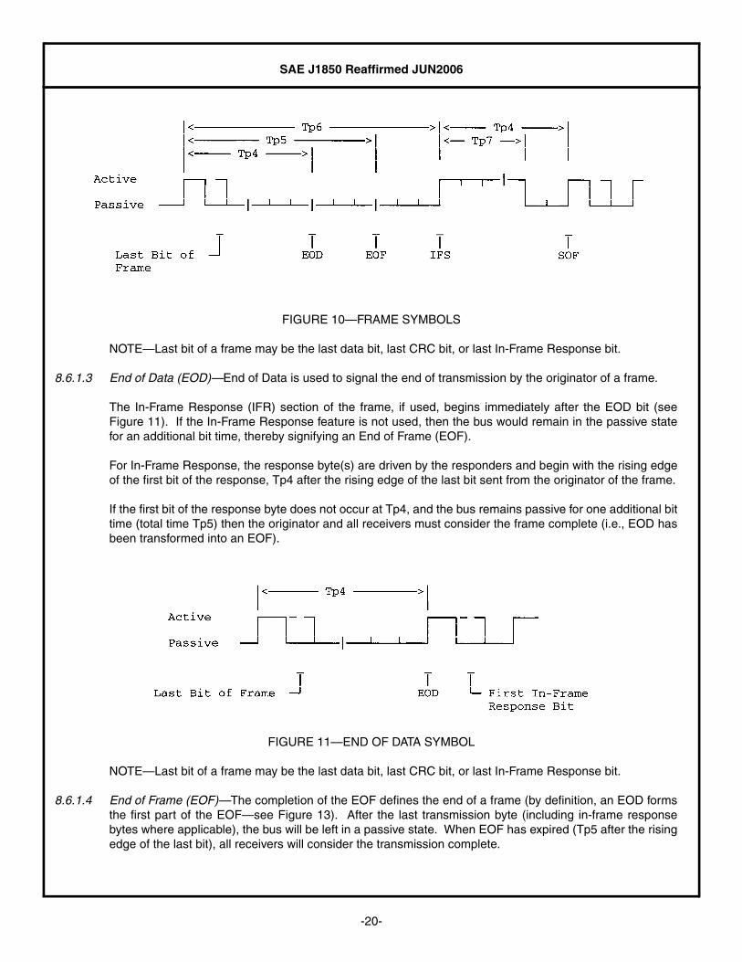
FIGURE 9—FRAME SYMBOLS
8.6.1.2 Start of Frame (SOF)—The Start of Frame (SOF) mark has the distinct purpose of uniquely determiningthe start of a frame (see Figure 10). The SOF is characterized by:
a. A reference rising edge that follows the previous rising edge by at least Tp5.b. A falling edge that occurs Tp7 after the reference rising edge.c. The rising edge of the first data bit will occur at Tp10 after the reference rising edge.
SAE J1850 Reaffirmed JUN2006
-20-
FIGURE 10—FRAME SYMBOLS
NOTE—Last bit of a frame may be the last data bit, last CRC bit, or last In-Frame Response bit.
8.6.1.3 End of Data (EOD)—End of Data is used to signal the end of transmission by the originator of a frame.
The In-Frame Response (IFR) section of the frame, if used, begins immediately after the EOD bit (seeFigure 11). If the In-Frame Response feature is not used, then the bus would remain in the passive statefor an additional bit time, thereby signifying an End of Frame (EOF).
For In-Frame Response, the response byte(s) are driven by the responders and begin with the rising edgeof the first bit of the response, Tp4 after the rising edge of the last bit sent from the originator of the frame.
If the first bit of the response byte does not occur at Tp4, and the bus remains passive for one additional bittime (total time Tp5) then the originator and all receivers must consider the frame complete (i.e., EOD hasbeen transformed into an EOF).
FIGURE 11—END OF DATA SYMBOL
NOTE—Last bit of a frame may be the last data bit, last CRC bit, or last In-Frame Response bit.
8.6.1.4 End of Frame (EOF)—The completion of the EOF defines the end of a frame (by definition, an EOD formsthe first part of the EOF—see Figure 13). After the last transmission byte (including in-frame responsebytes where applicable), the bus will be left in a passive state. When EOF has expired (Tp5 after the risingedge of the last bit), all receivers will consider the transmission complete.
SAE J1850 Reaffirmed JUN2006
-21-
8.6.1.5 Inter-Frame Separation (IFS)—Inter-Frame Separation allows proper synchronization of various nodesduring back-to-back frame operation.
A transmitter that desires bus access must wait for either of two conditions before transmitting a SOF:
a. IFS minimum has expired. (Tp6 after the rising edge of the last bit).b. EOF minimum and another rising edge has been detected. (Tp5 after the rising edge of the last bit).
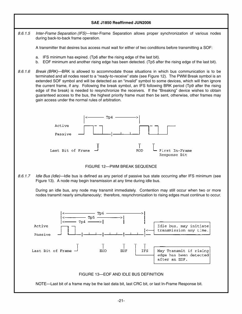
8.6.1.6 Break (BRK)—BRK is allowed to accommodate those situations in which bus communication is to beterminated and all nodes reset to a “ready-to-receive” state (see Figure 12). The PWM Break symbol is anextended SOF symbol and will be detected as an “invalid” symbol to some devices, which will then ignorethe current frame, if any. Following the break symbol, an IFS following BRK period (Tp9 after the risingedge of the break) is needed to resynchronize the receivers. If the “Breaking” device wishes to obtainguaranteed access to the bus, the highest priority frame must then be sent, otherwise, other frames maygain access under the normal rules of arbitration.
FIGURE 12—PWM BREAK SEQUENCE
8.6.1.7 Idle Bus (Idle)—Idle bus is defined as any period of passive bus state occurring after IFS minimum (seeFigure 13). A node may begin transmission at any time during idle bus.
During an idle bus, any node may transmit immediately. Contention may still occur when two or morenodes transmit nearly simultaneously; therefore, resynchronization to rising edges must continue to occur.
FIGURE 13—EOF AND IDLE BUS DEFINITION
NOTE—Last bit of a frame may be the last data bit, last CRC bit, or last In-Frame Response bit.
SAE J1850 Reaffirmed JUN2006
-22-
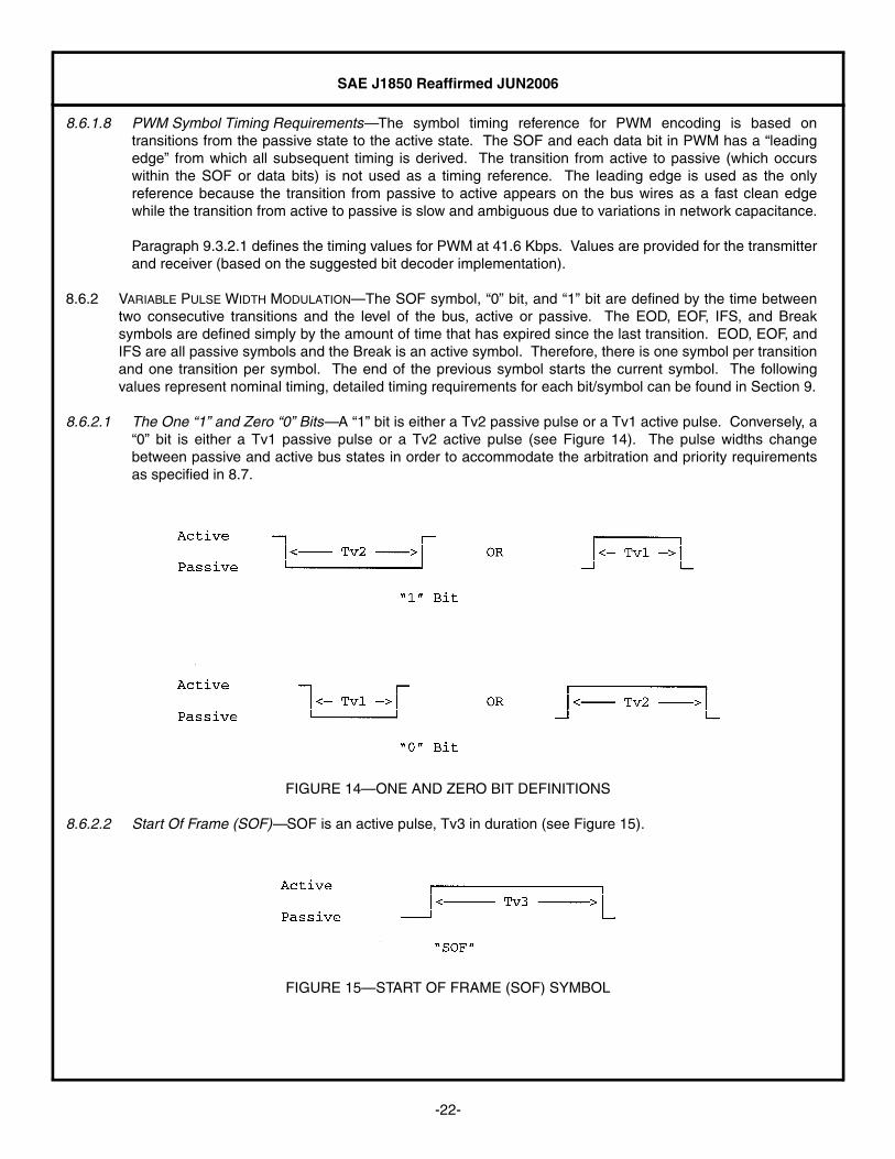
8.6.1.8 PWM Symbol Timing Requirements—The symbol timing reference for PWM encoding is based ontransitions from the passive state to the active state. The SOF and each data bit in PWM has a “leadingedge” from which all subsequent timing is derived. The transition from active to passive (which occurswithin the SOF or data bits) is not used as a timing reference. The leading edge is used as the onlyreference because the transition from passive to active appears on the bus wires as a fast clean edgewhile the transition from active to passive is slow and ambiguous due to variations in network capacitance.
Paragraph 9.3.2.1 defines the timing values for PWM at 41.6 Kbps. Values are provided for the transmitterand receiver (based on the suggested bit decoder implementation).
8.6.2 VARIABLE PULSE WIDTH MODULATION—The SOF symbol, “0” bit, and “1” bit are defined by the time betweentwo consecutive transitions and the level of the bus, active or passive. The EOD, EOF, IFS, and Breaksymbols are defined simply by the amount of time that has expired since the last transition. EOD, EOF, andIFS are all passive symbols and the Break is an active symbol. Therefore, there is one symbol per transitionand one transition per symbol. The end of the previous symbol starts the current symbol. The followingvalues represent nominal timing, detailed timing requirements for each bit/symbol can be found in Section 9.
8.6.2.1 The One “1” and Zero “0” Bits—A “1” bit is either a Tv2 passive pulse or a Tv1 active pulse. Conversely, a“0” bit is either a Tv1 passive pulse or a Tv2 active pulse (see Figure 14). The pulse widths changebetween passive and active bus states in order to accommodate the arbitration and priority requirementsas specified in 8.7.
FIGURE 14—ONE AND ZERO BIT DEFINITIONS
8.6.2.2 Start Of Frame (SOF)—SOF is an active pulse, Tv3 in duration (see Figure 15).
FIGURE 15—START OF FRAME (SOF) SYMBOL
SAE J1850 Reaffirmed JUN2006
-23-
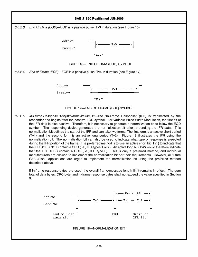
8.6.2.3 End Of Data (EOD)—EOD is a passive pulse, Tv3 in duration (see Figure 16).
FIGURE 16—END OF DATA (EOD) SYMBOL
8.6.2.4 End of Frame (EOF)—EOF is a passive pulse, Tv4 in duration (see Figure 17).
FIGURE 17—END OF FRAME (EOF) SYMBOL
8.6.2.5 In-Frame Response Byte(s)/Normalization Bit—The “In-Frame Response” (IFR) is transmitted by theresponder and begins after the passive EOD symbol. For Variable Pulse Width Modulation, the first bit ofthe IFR data is also passive. Therefore, it is necessary to generate a normalization bit to follow the EODsymbol. The responding device generates the normalization bit prior to sending the IFR data. Thisnormalization bit defines the start of the IFR and can take two forms. The first form is an active short period(Tv1) and the second form is an active long period (Tv2). Figure 18 illustrates the IFR using thenormalization bit. The normalization bit can also be used to indicate what type of response is expectedduring the IFR portion of the frame. The preferred method is to use an active short bit (Tv1) to indicate thatthe IFR DOES NOT contain a CRC (i.e., IFR types 1 or 2). An active long bit (Tv2) would therefore indicatethat the IFR DOES contain a CRC (i.e., IFR type 3). This is only a preferred method, and individualmanufacturers are allowed to implement the normalization bit per their requirements. However, all futureSAE J1850 applications are urged to implement the normalization bit using the preferred methoddescribed above.
If in-frame response bytes are used, the overall frame/message length limit remains in effect. The sumtotal of data bytes, CRC byte, and in-frame response bytes shall not exceed the value specified in Section9.
FIGURE 18—NORMALIZATION BIT
SAE J1850 Reaffirmed JUN2006
-24-
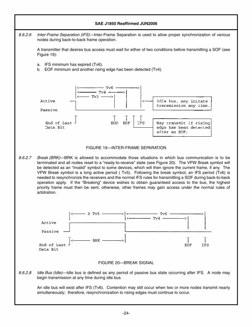
8.6.2.6 Inter-Frame Separation (IFS)—Inter-Frame Separation is used to allow proper synchronization of variousnodes during back-to-back frame operation.
A transmitter that desires bus access must wait for either of two conditions before transmitting a SOF (seeFigure 19):
a. IFS minimum has expired (Tv6).b. EOF minimum and another rising edge has been detected (Tv4).
FIGURE 19—INTER-FRAME SEPARATION
8.6.2.7 Break (BRK)—BRK is allowed to accommodate those situations in which bus communication is to beterminated and all nodes reset to a “ready-to-receive” state (see Figure 20). The VPW Break symbol willbe detected as an “invalid” symbol to some devices, which will then ignore the current frame, if any. TheVPW Break symbol is a long active period ( Tv5). Following the break symbol, an IFS period (Tv6) isneeded to resynchronize the receivers and the normal IFS rules for transmitting a SOF during back-to-backoperation apply. If the “Breaking” device wishes to obtain guaranteed access to the bus, the highestpriority frame must then be sent, otherwise, other frames may gain access under the normal rules ofarbitration.
FIGURE 20—BREAK SIGNAL
8.6.2.8 Idle Bus (Idle)—Idle bus is defined as any period of passive bus state occurring after IFS. A node maybegin transmission at any time during idle bus.
An idle bus will exist after IFS (Tv6). Contention may still occur when two or more nodes transmit nearlysimultaneously; therefore, resynchronization to rising edges must continue to occur.

SAE J1850 Reaffirmed JUN2006
-25-
8.6.2.9 VPW Symbol Timing Requirements—The most important factor in symbol timing uncertainty is the edgeposition uncertainty due to the time taken to make a transition between Vol,max and Voh,min (in eitherdirection). The maximum allowable transition time, Tt,max (the area between Vol,max and Voh,min), boundsthe time span between the earliest and latest node to recognize a transition and is a key design parameter.As Tt,max is reduced it becomes more and more difficult to design a driver which also meets the necessaryEMI requirements. In this manner, the corners of the waveform, which are a major contributor to theradiated contents of the signal, do not fall within the limits imposed by Tt,max as found in Section 9.
Other factors that affect the transmitted pulse width are oscillator tolerance and variations in delay throughthe receiver, noise filter, and driver. For a fixed oscillator and a well-designed digital filter, most of thevariation is in the time it takes the driver to leave the current state and start the transition. The variousfactors (plus some guard band and allowance for alternative implementations) can be lumped into a singleset of limits, Tx,min and Tx,max, for each symbol. Each is measured from the trip point of the previoustransition as seen by the transmitting node (assuming a step input) to the beginning or end of the transitionat Voh,min or Vol,max.
The pulse width as seen by another node, which may perceive the leading edge either sooner or later thanthe transmitting node, can range from Tx,min – Tt,max to Tx,max + Tt,max in absolute terms. This rangerepresents a receiver's required acceptance range for a given symbol. The actual acceptance range mustbe wider to allow for receiver oscillator tolerance and any implementation-dependent uncertainties orconstraints. The necessary guard band limits how close together symbols can be defined. To keep thesymbols short, there is no space allocated for an unambiguous (with normal tolerances) forbidden zonebetween symbols.
The time windows are not affected by multiple nodes trying to transmit at the same time during arbitration.This is because a single node effectively dominates each transition. It is either the first node to leave thepassive state or the last node to leave the active state. Although the fastest or slowest node dominates aparticular transition, the contention scheme assures that the highest priority frame always wins regardlessof which node started transmitting first.
The purpose of the noise filter is to eliminate impulse noise which may exceed the steady-state noisemargin and to minimize the need for hysteresis at the receiver input. The delay through the filter iscompensated for in the timing logic. A specific implementation of the filter is not required for compatibilityso long as the delay is properly compensated and the uncertainty bounds are not exceeded. In thepresence of arbitrary noise during the transition period, the filter should respond as though a single stepinput had occurred at some point within that period.
The symbol limits defined in Section 9 are consistent with Tt,max and the specified oscillator tolerance.Tnom is the nominal symbol time with no oscillator error and the receiver detecting the transition at Vt (seeanalysis in Appendix D).
8.7 Contention/Arbitration/Priority—A contention situation arises when more than one node attempts to accessthe bus at essentially the same time.
8.7.1 CONTENTION DETECTION—Contention detection is the recognition of conflicting symbols or bits. The processof bit-by-bit arbitration allows conflicting frame transmissions to be detected. A node that detects a differencebetween the symbol or bit it receives and the symbol or bit it is currently transmitting has detected contentionto the transmission of its frame. Only the one frame that wins all conflicts of different symbols and bits withall the other nodes that began transmitting during that frame will not detect contention.
SAE J1850 Reaffirmed JUN2006
-26-
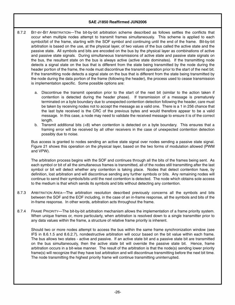
8.7.2 BIT-BY-BIT ARBITRATION—The bit-by-bit arbitration scheme described as follows settles the conflicts thatoccur when multiple nodes attempt to transmit frames simultaneously. This scheme is applied to eachsymbol/bit of the frame, starting with the SOF symbol and continuing until the end of the frame. Bit-by-bitarbitration is based on the use, at the physical layer, of two values of the bus called the active state and thepassive state. All symbols and bits are encoded on the bus by the physical layer as combinations of activeand passive state signals. During simultaneous transmissions of active state and passive state signals onthe bus, the resultant state on the bus is always active (active state dominates). If the transmitting nodedetects a signal state on the bus that is different from the state being transmitted by the node during theheader portion of the frame, the node must discontinue the transmit operation prior to the start of the next bit.If the transmitting node detects a signal state on the bus that is different from the state being transmitted bythe node during the data portion of the frame (following the header), the process used to cease transmissionis implementation specific. Some possible options are:
a. Discontinue the transmit operation prior to the start of the next bit (similar to the action taken ifcontention is detected during the header phase). If transmission of a message is prematurelyterminated on a byte boundary due to unexpected contention detection following the header, care mustbe taken by receiving nodes not to accept the message as a valid one. There is a 1 in 256 chance thatthe last byte received is the CRC of the previous bytes and would therefore appear to be a validmessage. In this case, a node may need to validate the received message to ensure it is of the correctlength.
b. Transmit additional bits (<8) when contention is detected on a byte boundary. This ensures that aframing error will be received by all other receivers in the case of unexpected contention detectionpossibly due to noise.
Bus access is granted to nodes sending an active state signal over nodes sending a passive state signal.Figure 21 shows this operation on the physical layer, based on the two forms of modulation allowed (PWMand VPW).
The arbitration process begins with the SOF and continues through all the bits of the frames being sent. Aseach symbol or bit of all the simultaneous frames is transmitted, all of the nodes still transmitting after the lastsymbol or bit will detect whether any contention is taking place. Nodes that detect contention have, bydefinition, lost arbitration and will discontinue sending any further symbols or bits. Any remaining nodes willcontinue to send their symbols/bits until the next contention is detected. The node which obtains sole accessto the medium is that which sends its symbols and bits without detecting any contention.
8.7.3 ARBITRATION AREA—The arbitration resolution described previously concerns all the symbols and bitsbetween the SOF and the EOF including, in the case of an in-frame response, all the symbols and bits of thein-frame response. In other words, arbitration acts throughout the frame.
8.7.4 FRAME PRIORITY—The bit-by-bit arbitration mechanism allows the implementation of a frame priority system.When unique frames or, more particularly, when arbitration is resolved down to a single transmitter prior toany data values within the frame, a structure of relative frame priority is inherent.
Should two or more nodes attempt to access the bus within the same frame synchronization window (seeIFS in 8.6.1.5 and 8.6.2.7), nondestructive arbitration will occur based on the bit value within each frame.The bus allows two states - active and passive. If an active state bit and a passive state bit are transmittedon the bus simultaneously, then the active state bit will override the passive state bit. Hence, framearbitration occurs in a bit-wise manner. The result of the arbitration is that the node(s) sending lower priorityframe(s) will recognize that they have lost arbitration and will discontinue transmitting before the next bit time.The node transmitting the highest priority frame will continue transmitting uninterrupted.

SAE J1850 Reaffirmed JUN2006
-27-
FIGURE 21—ARBITRATION
Based on the bit definitions contained in 8.6, the lowest value bytes immediately following the SOF will havethe highest priority. Therefore, regardless of the number of bits allocated for “frame prioritization,” thenumerical value of zero will have the absolutely highest priority (that is, 000 is higher priority than 001 or111).
8.8 Node Wake-Up Via Physical Layer—The transition to a functional/operating network from an unpowered orstandby state is a common occurrence in vehicle multiplex systems. In the context of this document theSession Layer controls the transitions between the operating and the standby states.
Two perspectives are used to define the session layer:
a. The view of the media itself, without regard to the individual nodes on the networkb. The view from an individual node
Both are required for a complete definition of the possible states of network operation.
It is expected that a typical vehicle multiplex system may contain a mixture of unpowered and powered nodes,and that the individual nodes may themselves have both powered and standby states.

SAE J1850 Reaffirmed JUN2006
-28-
8.8.1 NETWORK MEDIA
8.8.1.1 Unbiased Network—An unbiased network is all conductors at ground voltage and the impedance of theconductors not controlled. No communication is possible on an unbiased network. The media must firstbe brought to the biased state before communication can take place. The transition of the network fromthe unbiased to the biased state may serve as a node wake-up signal for certain applications, but this is nota requirement (i.e., it is possible for individual nodes to be in the sleep state on a fully biased network or inthe awake state on an unbiased network).
8.8.1.2 Biased Network—A biased network is all conductors at the “passive” voltage level (with no communicationoccurring) and with appropriate impedances capable of supporting communication. Individual nodes onthe network may exist in any of the three states described as follows. Note that nodes which use theoptional sleep state are required to wake up from the appropriate network signal within a defined wake-upperiod. In other words, all nodes which are capable of wake-up from network signals must do so;otherwise these nodes are considered “unpowered.” This requirement assures a finite and limited delay toestablish communication with nodes which may be in the sleep state.
The time required for the media to make the transition from the unbiased to the biased state is not definedin this document, since this parameter is largely application dependent and, in fact, may not even occur(e.g., media always biased). For the same reason, the time required for a node to make the transitionbetween the unpowered state and the sleep or awake state is also not defined.
8.8.2 INDIVIDUAL NODES
8.8.2.1 Unpowered Node—An unpowered node is not capable of network communication, nor wake-up fromnetwork signal transitions.
8.8.2.2 Sleeping Node—A sleeping node may have an optional low-power standby mode capable of detectingnetwork signal transitions for the purpose of wake-up. Any interface device in the sleep state can beawakened by any other interface device via network activity or awakened by its host via its interface to thehost. There is no specified requirement for the transition from the awake state to the sleep state, since thisis an implementation-specific issue.
8.8.2.3 Awake/Operational—An awake/operational node is fully capable of receiving and transmitting frames onthe network. The maximum amount of time from the wake-up stimulus until the node is capable ofcommunicating is implementation specific. A transition of the bus from the passive state to the active stateshall be considered a “wake-up” signal to a sleeping node. Proper bus bias must be supplied by all nodesdesignated to supply bias when the network is powered.
8.9 Physical Layer Fault Considerations
8.9.1 REQUIRED FAULT TOLERANT MODES—The network must meet the requirements as defined per the followingfailure modes:
a. Node Power Loss—All nodes must continue to meet the network leakage current requirement during aloss of power (or low voltage) condition.
b. Bus Short to Ground—Network data communications may be interrupted but there shall be no damageto any node when the bus is shorted to ground.
c. Bus Short to Battery—Network data communications may be interrupted but there shall be no damage toany node when the bus is shorted to battery power.
d. Loss of Node Connection to Ground—When a node loses its ground connection, the remaining nodesshall remain capable of communications.

SAE J1850 Reaffirmed JUN2006
-29-
8.9.2 OPTIONAL FAULT TOLERANT MODES—The network may optionally meet the requirements as defined per thefollowing failure modes:
a. Loss of Termination/Bias—Biasing and termination resistors shall be redundant such that no single pointfailure will cause the network to become inoperative.
b. Loss of Connection to Network—When a node becomes disconnected from the network the remainingnodes shall remain capable of communications.
c. Dual Wire Fault Tolerant Operation—Nodes on a dual wire bus may be capable of full communication(sending and receiving frames) at the specified bit rate in the presence of any one of the following faultsoccurring anywhere on the network:
1. Bus “+” wire Open Circuit2. Bus “–” wire Open Circuit3. Bus “+” wire Shorted to Ground4. Bus “–” wire Shorted to Ground5. Bus “+” wire Shorted to Battery + (Vbatt)6. Bus “–” wire Shorted to Battery + (Vbatt)7. Bus “+” wire Shorted to any voltage between Ground and Battery8. Bus “–” wire Shorted to any voltage between Ground and Battery
Noise immunity and emissions may be somewhat degraded during the faulted period but shall return tonormal after the fault is removed.
All nodes shall be protected from damage during the presence of these faults such that recovery to normaloperation occurs automatically upon removal of the fault (i.e., faults shall not propagate through the network).
Continued communication is not required for the “Double Fault” condition of the Bus “+” wire shorted to theBus “–” wire.
8.10 EMC Requirements—The vehicle manufacturer shall specify a minimum EMC level of operation for a modulethat utilizes this network interface device. A philosophical method for classification of functional performancecan be found in SAE J1113 Part 1 Appendix B (formerly SAE J1113 Appendix B). A component manufacturerthat designs the interface device to conform to the most severe classification of Class C Region I, for example,could be assured of adequate performance for all conditions.
The modules that communicate with each other via this interface device shall not generate levels of noiseemissions (EMI) large enough to interfere with each other. For reference, the levels defined by CISPR/D/WG2(Secretariat) 19 Sept 1989 may be used. In general, the specifications on wave shaping and transition rise andfall times control the EMI levels.
The vehicle manufacturers may find SAE J1211 helpful in specifying their multiplex systems. SAE J1879 mayalso be utilized for specifying components.This document recommends the vehicle manufacturers use thefollowing documents and the outlined EMC test plan defined in Appendix B. EMC and voltage “level”requirements specified by the Test Plan are given for reference only and the vehicle manufacturerspecifications shall be used for compliance testing.
a. Radiated Emissions Antenna & Probe Test (CISPR/D/WG2(Secretariat) 19 Sept 1989)b. Transfer Function, Current probe monitoring (SAE J1113 Part 2)c. Transfer Function, Antenna monitoring (SAE J1113 Part 3)d. RF Susceptibility (SAE J1113 Part 13)e. Transient Susceptibility (SAE J1113 Part 10)
SAE J1850 Reaffirmed JUN2006
-30-
9. Parameters
9.1 Application Layer—The following Application Layer requirements shall exist whenever the network is used.
Bit Dominance - A “0” bit dominates over a “1” bit.
9.2 Data Link Layer
9.2.1 PULSE WIDTH MODULATION (PWM) AT 41.6 KBPS—The maximum frame length from SOF to EOF inclusive is101 bit times. The maximum number of message bytes (i.e., excluding frame delimiters SOF, EOD, EOF, andIFS) is 12 bytes.
9.2.2 VARIABLE PULSE WIDTH (VPW) AT 10.4 KBPS—The maximum number of message bytes (i.e., excludingframe delimiters SOF, EOD, EOF, and IFS) is 12 bytes.
9.3 Physical Layer
9.3.1 GENERAL NETWORK REQUIREMENTS (SEE TABLE 2)
9.3.2 PULSE WIDTH MODULATION (PWM)
9.3.2.1 PWM Timing Requirements—The following requirements, see Table 3, are for a nominal bit time of 24 msor 41.6 Kbps as seen on the network media.
TABLE 2—GENERAL NETWORK PARAMETERS
Parameter Description Parameter Value
On-Vehicle Network Length 35 meters(1)
1. For VPW, the On-Vehicle Network Length and the Total Vehicle Network Length are for reference use. For PWM, these lengths specified shall not be exceeded.
Off-Vehicle Network Length 5 meters
Total Vehicle Network Length 40 meters(1)
Maximum number of standard unit loads(including off-vehicle equipment)
32 nodes
Off-vehicle load resistance 10.6 kohms min
Off-vehicle capacitance(each bus wire to signal or chassis ground, as measured atthe SAE J1962 connector)
500 pF max

SAE J1850 Reaffirmed JUN2006
-31-
Transmit tolerances include oscillator tolerances, physical layer delays (i.e., turn-on and turn-off delays),and other miscellaneous tolerances. Receive tolerances include considerations for voltage offsetsbetween transmitter and receiver and other miscellaneous tolerances.Symbols received in the “gray” areaspreviously can be decoded as either the symbol before or after that of the “gray” area. For example, anactive pulse of 12.5 µs can be decoded as either an active phase “1” (Tp1) or an active phase “0” (Tp2).An incorrect decision will be detected in the CRC error detection byte. Figure 22 gives an example of howa signal should be decoded based on the received pulse width.
FIGURE 22—EXAMPLE OF RECEIVING A TP1 OR TP2 SYMBOL
TABLE 3—PWM PULSE WIDTH TIMES (µs)
Symbol Tx,min Tx,nom Tx,max Rx,min Rx,max
Tp1: Active phase “1” ≥ 7 8 ≤ 9 ≥ 6 ≤ 11
Tp2: Active phase “0” ≥ 15 16 ≤ 17 ≥ 14 ≤ 19
Tp3: Bit time ≥ 23 24 ≤ 25.5 ≥ 22 ≤ 27
Tp4: SOF/EOD time ≥ 47 48 ≤ 51 ≥ 46 ≤ 63
Tp5: EOF time ≥ 70 72 76.5 ≥ 70 N/A(1)
1. EOF transitions into IFS and is not actually a “transmitted” symbol.
Tp6: IFS time ≥ 94 96 N/A(2)
2. Maximum IFS ends at next SOF.
N/A N/A(2)
Tp7: Active SOF ≥ 30 32 ≤ 33 ≥ 30 ≤ 35
Tp8: Active BRK ≥ 38 40 ≤ 41 ≥ 38 ≤ 43
Tp9: BRK to IFS time ≥118 120 N/A(2) N/A N/A(2)
Tp10: SOF to Data rising edge ≥ 47 48 ≤ 51 ≥ 45 ≤ 52
TP11 Passive to next rising edge ≥ 6 N/A N/A ≥ 4 N/A
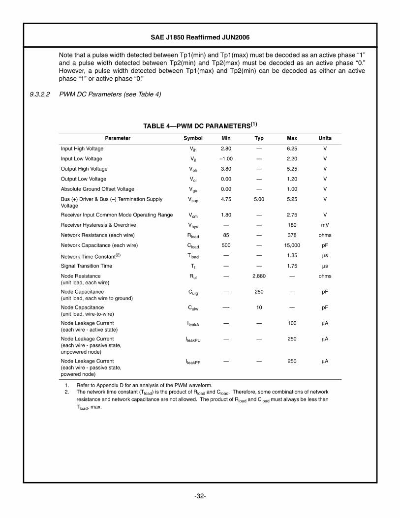
SAE J1850 Reaffirmed JUN2006
-32-
Note that a pulse width detected between Tp1(min) and Tp1(max) must be decoded as an active phase “1”and a pulse width detected between Tp2(min) and Tp2(max) must be decoded as an active phase “0.”However, a pulse width detected between Tp1(max) and Tp2(min) can be decoded as either an activephase “1” or active phase “0.”
9.3.2.2 PWM DC Parameters (see Table 4)
TABLE 4—PWM DC PARAMETERS(1)
1. Refer to Appendix D for an analysis of the PWM waveform.
Parameter Symbol Min Typ Max Units
Input High Voltage Vih 2.80 — 6.25 V
Input Low Voltage Vil –1.00 — 2.20 V
Output High Voltage Voh 3.80 — 5.25 V
Output Low Voltage Vol 0.00 — 1.20 V
Absolute Ground Offset Voltage Vgo 0.00 — 1.00 V
Bus (+) Driver & Bus (–) Termination Supply Voltage
Vsup 4.75 5.00 5.25 V
Receiver Input Common Mode Operating Range Vcm 1.80 — 2.75 V
Receiver Hysteresis & Overdrive Vhys — — 180 mV
Network Resistance (each wire) Rload 85 — 378 ohms
Network Capacitance (each wire) Cload 500 — 15,000 pF
Network Time Constant(2)
2. The network time constant (Tload) is the product of Rload and Cload. Therefore, some combinations of network resistance and network capacitance are not allowed. The product of Rload and Cload must always be less than Tload, max.
Tload — — 1.35 µs
Signal Transition Time Tt — — 1.75 µs
Node Resistance(unit load, each wire)
Rul — 2,880 — ohms
Node Capacitance(unit load, each wire to ground)
Culg — 250 — pF
Node Capacitance(unit load, wire-to-wire)
Culw —- 10 — pF
Node Leakage Current(each wire - active state)
IleakA — — 100 µA
Node Leakage Current(each wire - passive state,unpowered node)
IleakPU — — 250 µA
Node Leakage Current(each wire - passive state,powered node)
IleakPP — — 250 µA
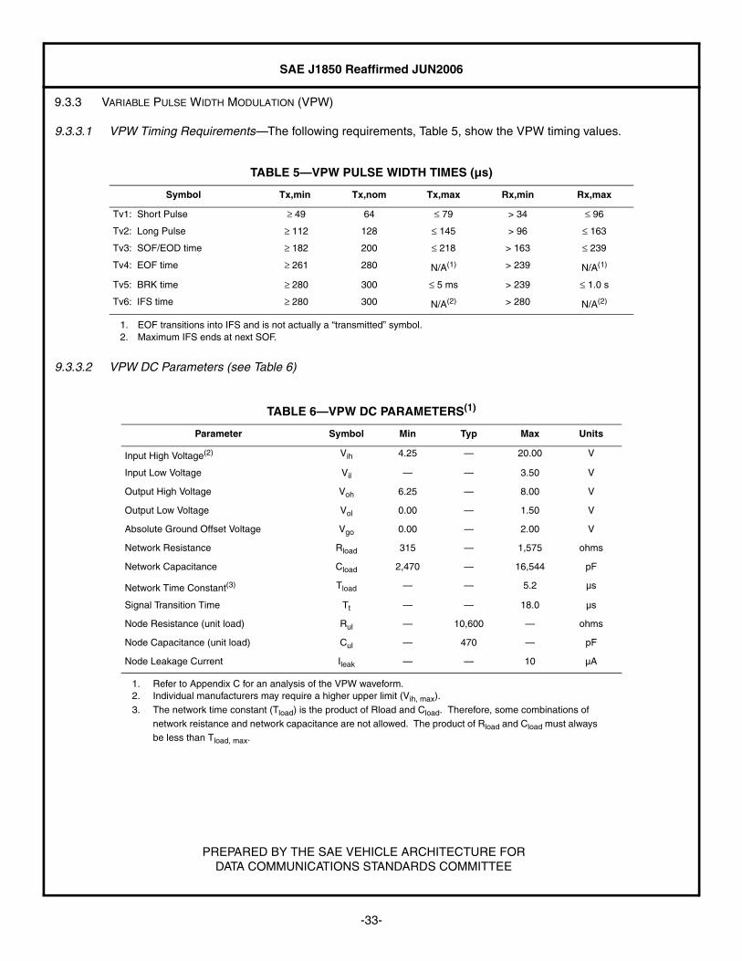
SAE J1850 Reaffirmed JUN2006
-33-
9.3.3 VARIABLE PULSE WIDTH MODULATION (VPW)
9.3.3.1 VPW Timing Requirements—The following requirements, Table 5, show the VPW timing values.
9.3.3.2 VPW DC Parameters (see Table 6)
PREPARED BY THE SAE VEHICLE ARCHITECTURE FORDATA COMMUNICATIONS STANDARDS COMMITTEE
TABLE 5—VPW PULSE WIDTH TIMES (µs)
Symbol Tx,min Tx,nom Tx,max Rx,min Rx,max
Tv1: Short Pulse ≥ 49 64 ≤ 79 > 34 ≤ 96
Tv2: Long Pulse ≥ 112 128 ≤ 145 > 96 ≤ 163
Tv3: SOF/EOD time ≥ 182 200 ≤ 218 > 163 ≤ 239
Tv4: EOF time ≥ 261 280 N/A(1)
1. EOF transitions into IFS and is not actually a “transmitted” symbol.
> 239 N/A(1)
Tv5: BRK time ≥ 280 300 ≤ 5 ms > 239 ≤ 1.0 s
Tv6: IFS time ≥ 280 300 N/A(2)
2. Maximum IFS ends at next SOF.
> 280 N/A(2)
TABLE 6—VPW DC PARAMETERS(1)
1. Refer to Appendix C for an analysis of the VPW waveform.
Parameter Symbol Min Typ Max Units
Input High Voltage(2)
2. Individual manufacturers may require a higher upper limit (Vih, max).
Vih 4.25 — 20.00 V
Input Low Voltage Vil — — 3.50 V
Output High Voltage Voh 6.25 — 8.00 V
Output Low Voltage Vol 0.00 — 1.50 V
Absolute Ground Offset Voltage Vgo 0.00 — 2.00 V
Network Resistance Rload 315 — 1,575 ohms
Network Capacitance Cload 2,470 — 16,544 pF
Network Time Constant(3)
3. The network time constant (Tload) is the product of Rload and Cload. Therefore, some combinations of network reistance and network capacitance are not allowed. The product of Rload and Cload must always be less than Tload, max.
Tload — — 5.2 µs
Signal Transition Time Tt — — 18.0 µs
Node Resistance (unit load) Rul — 10,600 — ohms
Node Capacitance (unit load) Cul — 470 — pF
Node Leakage Current Ileak — — 10 µA

SAE J1850 Reaffirmed JUN2006
-34-
APPENDIX A
CHECKLIST OF APPLICATION-SPECIFIC FEATURES
A.1 Figure A1 is a checklist provided as an aid to highlight the communication features of J1850.
FIGURE A1A—CHECKLIST OF APPLICATION-SPECIFIC FEATURES

SAE J1850 Reaffirmed JUN2006
-35-
FIGURE A1B—CHECKLIST OF APPLICATION-SPECIFIC FEATURES (CONTINUED)
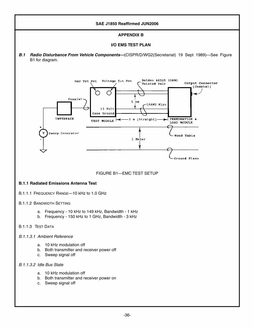
SAE J1850 Reaffirmed JUN2006
-36-
APPENDIX B
I/O EMS TEST PLAN
B.1 Radio Disturbance From Vehicle Components—(CISPR/D/WG2(Secretariat) 19 Sept 1989)—See FigureB1 for diagram.
FIGURE B1—EMC TEST SETUP
B.1.1 Radiated Emissions Antenna Test
B.1.1.1 FREQUENCY RANGE—10 kHz to 1.0 GHz
B.1.1.2 BANDWIDTH SETTING
a. Frequency - 10 kHz to 149 kHz, Bandwidth - 1 kHzb. Frequency - 150 kHz to 1 GHz, Bandwidth - 3 kHz
B.1.1.3 TEST DATA
B.1.1.3.1 Ambient Reference
a. 10 kHz modulation offb. Both transmitter and receiver power offc. Sweep signal off
B.1.1.3.2 Idle Bus State
a. 10 kHz modulation offb. Both transmitter and receiver power onc. Sweep signal off
SAE J1850 Reaffirmed JUN2006
-37-
B.1.1.3.3 Active Bus State
a. 10 kHz modulation onb. Both transmitter and receiver power onc. Sweep signal off
B.1.2 Radiated Emissions Probe Test
B.1.2.1 FREQUENCY RANGE—10 kHz to 200 MHz
B.1.2.2 BANDWIDTH SETTING
a. Frequency - 10 kHz to 149 kHz, Bandwidth - 1 kHzb. Frequency - 150 kHz to 1 GHz, Bandwidth - 3 kHz
B.1.2.3 PROBE TYPE—As required to make measurements
a. Recommended probe type - Tektronix A6302 (0 - 29 MHz)b. Recommended probe type - Ailtech 94111-1 (30 - 200 MHz)
B.1.2.4 PROBE DISTANCE—5 cm from part
B.1.2.5 TEST DATA
B.1.2.5.1 Ambient Reference
a. 10 kHz modulation offb. Both transmitter and receiver power offc. Sweep signal off
B.1.2.5.2 Idle State
a. 10 kHz modulation offb. Both transmitter and receiver power onc. Sweep signal off
B.1.2.5.3 Active Bus
a. 10 kHz modulation onb. Both transmitter and receiver power onc. Sweep signal off
B.2 Transfer FunctionElectromagnetic Susceptibility Measurement Procedures for Vehicle Components
B.2.1 Current Probe Monitoring—Adapted from SAE J1113 Part 2 (Formerly SAE J1113 (Aug 87) Section 2).
a. Frequency - 30 Hz to 250 kHzb. Amplitude - 1 V peak-to-peak at test point
B.2.2 Antenna Monitoring—Adapted from SAE J1113 Part 3 (Formerly SAE J1113 (Aug 87) Section 3).
a. Frequency: 250 kHz to 200 MHzb. Attenuator input power:»25 mW to generate 1 V peak-to-peak at test point
SAE J1850 Reaffirmed JUN2006
-38-
B.2.3 Test Data
B.2.3.1 TRANSFER FUNCTION FROM VCC TO BUS
a. 10 kHz modulation onb. Both transmitter and receiver power onc. Sweep signal on
B.2.3.2 TRANSFER FUNCTION FROM GROUND TO BUS
a. 10 kHz modulation onb. Both transmitter and receiver power onc. Sweep signal on
B.3 RF Susceptibility—Electromagnetic Susceptibility Measurement Procedures for Common Mode Injection forcompliance, test per SAE J1113 Part 13 (formerly SAE J1547).
B.3.1 Frequency Range—1 MHz to 200 MHz.
B.3.2 Max Level—100 mA RMS.
B.3.3 Procedure—Injection and monitoring to be applied to Bus pair only.
B.3.4 Test Data—Record the nature of any interaction occurring below the test level along with the current andfrequency.
B.4 Transient Susceptibility—Test per SAE J1113 Part 12 (Adapted from ISO 7637/3).
Test Pulse Amplitude
a. Test Pulse 1: –30 V (Reference)b. Test Pulse 2: +30 V (Reference)c. Test Pulse 3a: –60 V (Reference)d. Test Pulse 3b: +40 Vs (Reference)
SAE J1850 Reaffirmed JUN2006
-39-
APPENDIX C
VPW WAVEFORM ANALYSIS
C.1 VPW Waveform Analysis—Figure C1 shows a drawing of a bus waveform with various voltage levels and trippoints. The voltage levels and trip points are defined as follows:
FIGURE C1—VOLTAGE LEVELS AND TRIP POINTS
C.2 Voltage Levels and Trip Points
C.2.1 Voh,min—Minimum guaranteed output high voltage. This is also the highest trip point, with the source havingno ground offset noise, and the receiver having 2 V of noise.
C.2.2 Vol,max—Maximum guaranteed output low voltage. This is also the lowest trip point, with the receiver havingno ground offset noise, and the source having 2 V of noise.
C.2.3 Vt—Ideal receiver trip point.
C.2.4 Vih,min—Minimum guaranteed input high voltage and is also the highest trip point with no offset noise.
C.2.5 Vil,max—Maximum guaranteed input low voltage and is also the lowest trip point with no offset noise.
C.3 VPW Pulse Width Analysis—Factors that affect the transmitted pulse width are oscillator tolerance andvariations in delay through the source driver and the medium. These factors, along with some guard banding,are lumped into a single set of limits called Tx,min and Tx,max for each bus symbol.
For a Tnom = Tx,nom, Equations C1 and C2 are used to generate the transmitted pulse values shown in TableC1:
(Eq. C1)
(Eq. C2)
Tx min, Tnom Tt max, 2⁄–( )∗0.98 Tx mar,–=
Tx max, Tnom Tt max, 2⁄+( )∗1.02 Tx mar,+=
SAE J1850 Reaffirmed JUN2006
-40-
The (Tnom ± Tt,max/2) * 2% factor covers the 2% oscillator tolerance. The Tx,nom and Tt,max factors are given inSection 9. The Tx,mar factor is assumed to be 5.0 which covers the rest of the factors (lumped variation in delaythrough the source driver and medium).
For VPW, node synchronization is an integral part of symbol timing. All transmitting nodes reference theirtransmit timing from their receiver's perception of the previous edge without regard to whether that edge wasdue to their own or another transmitter.
Figure C2 shows a plot of Tx, (i.e., Tx,min and Tx,max). Each is measured from the ideal trip point on the leadingedge of the waveform. The fact that what is seen at the source's own receiver contributes to the transmittedpulse width, implies that the source device could be using echoed back information to shape what istransmitted.
The pulse width seen by another node (receiver) can range from Tx,min – Tt,max to Tx,max + Tt,max. This rangecomes from the variations in the transmitted pulse width combined with possible noise offset effects on thetransmitted and receiving node. The Tx,min – Tt,max situation occurs when a Tx,min pulse width is transmitted bya source node with no ground offset noise, and received by a receiving node with a 2 V of ground offset noise.This sets up the possibility of the receiver tripping at Voh,min on the leading and trailing edge of the waveform.Therefore the pulse width seen by another node for this Tx,min – Tt,max situation including the oscillatortolerance and guard banding is given by Equation C4. Equation C5 is derived by substituting Equation C1 forTx,min into Equation C4. Equation C6 is derived by including the effect of the real receiver trip point Ttp,max inEquation C1 and substituting for Tx,min in Equation C4. The Tt,max/2 factor is equal to zero, in Equation C6,since an ideal trip point and no ground offset was assumed. The Tx,max + Tt,max situation occurs with a Tx,maxpulse being transmitted, the source node having 2 V of noise, and the receiver having no offset. This sets upthe possibility of the receiving node tripping at Vol,max. Again the actual acceptance range must be wider toallow for the receiving node's oscillator tolerance and any implementation dependent uncertainties orconstraints. Similarly Equations C9 and C10 are derived.
The receiving node may perceive the leading edge sooner or later than the transmitting node (source node).This range represents a receiver's required acceptance range for a given bus symbol. Figure C2 shows adrawing of this acceptance range.
TABLE C1—VPW PULSE WIDTH TIMES (MS)
Symbol Tx,min Tx,nom Tx,max Rx,min Rx,max
Tv1: Short Pulse 49 64 79 34 96
Tv2: Long Pulse 112 128 145 95 162
Tv3: SOF/EOD time 182 200 218 164 237
Tv4: EOF time 261 280 N/A 241 N/A
SAE J1850 Reaffirmed JUN2006
-41-
FIGURE C2—WAVEFORM TIMING PARAMETERS
The calculations for the received Tr,min and Tr,max are derived using the factors specified in Section 9 for a 2 Vground offset range and a transition rise time of Tt,max. The transmitting node Tt,max factor would be zero (0) ifit was a perfect receiver and sensed a transition at the ideal trip point. However, for a real receiver the trip pointTtp,max can be approximated by Equation C3 assuming a linear waveform rise time.
(Eq. C3)
The values for this range shown in Table C1 were arrived at using Equations C7 and C11. Note these valuescompare favorably with the values specified in Section 9, Table 5.
(Eq. C4)
Ttp max, Tt max, ∗ Vih min, Vil max,–( ) Voh min, Vol max,–( )⁄( )=
Tr min, Tx min, Tt max,–( )∗0.98 Tr mar,–=
SAE J1850 Reaffirmed JUN2006
-42-
(Eq. C5)
NOTE—Equation C5 does not consider the effect of the rear receiver trip point, Ttp,max. Equation C6 is derivedby including Ttp,max in Equation C1 and substituting for Tx,min in Equation C4.
(Eq. C6)
NOTE—Since an ideal trip point and no ground offset are assumed, the Tt,max/2 factor is set to zero(0),producing Equation C7.
(Eq. C7)
(Eq. C8)
(Eq. C9)
(Eq. C10)
(Eq. C11)
The 2% guard bands cover the oscillator tolerances of both transmitter and receiver and Tr,mar = 4.0 covers theother uncertainties, including receiver delay and digital filter delay. VPW bus symbols allow no forbidden zonesbetween symbols.
Table C1 shows the VPW Pulse Width Timing Requirements
Filter Compensation—The reason for choosing a synchronous data encoding technique is to synchronize atevery valid state transition. If the delays through the filter, receiver, and output drivers can be characterizedinto a constant value, this delay can be compensated for by the timing logic. If variations in delay caused bythis Filter and I/O Hardware cannot be easily compensated for, then the Source Interface device variationsshould be included in the ±5.0 µs factor defined in Tx,min and Tx,max. All further, variations in delay andincluding a safety factor for dead zones between symbols for the Receiving device should be included in the ±4ms factor defined in Tr,min and Tr,max.
Tr min, Tnom Tt max, 2⁄–( )∗0.98 Tx mar,–[ ] Tt max,–( )∗0.98 Tr mar,–=
Tr min, Tnom Tt max, 2 Ttp max, 2⁄–⁄–( )∗0.98 Tx mar,–[ ] Tt max,–( )∗0.98 Tr mar,–=
Tr min, Tnom Ttp max, 2⁄–( )∗0.98 Tx mar,–[ ] Tt max,–( )∗0.98 Tr mar,–=
Tr max, Tx max, Tt max,+( )∗1.02 Tr mar,+=
Tr max, Tnom Tt max, 2⁄+( )∗1.02 Tx mar,+[ ] Tt max,+( )∗1.02 Tr mar,+=
Tr max, Tnom Tt max, 2 Ttp max, 2⁄+⁄+( )∗1.02 Tx mar,+[ ] Tt max,+( )∗1.02 Tr mar,+=
Tr max, Tnom Ttp max, 2⁄+( )∗1.02 Tx mar,+[ ] Tt max,+( )∗1.02 Tr mar,+=
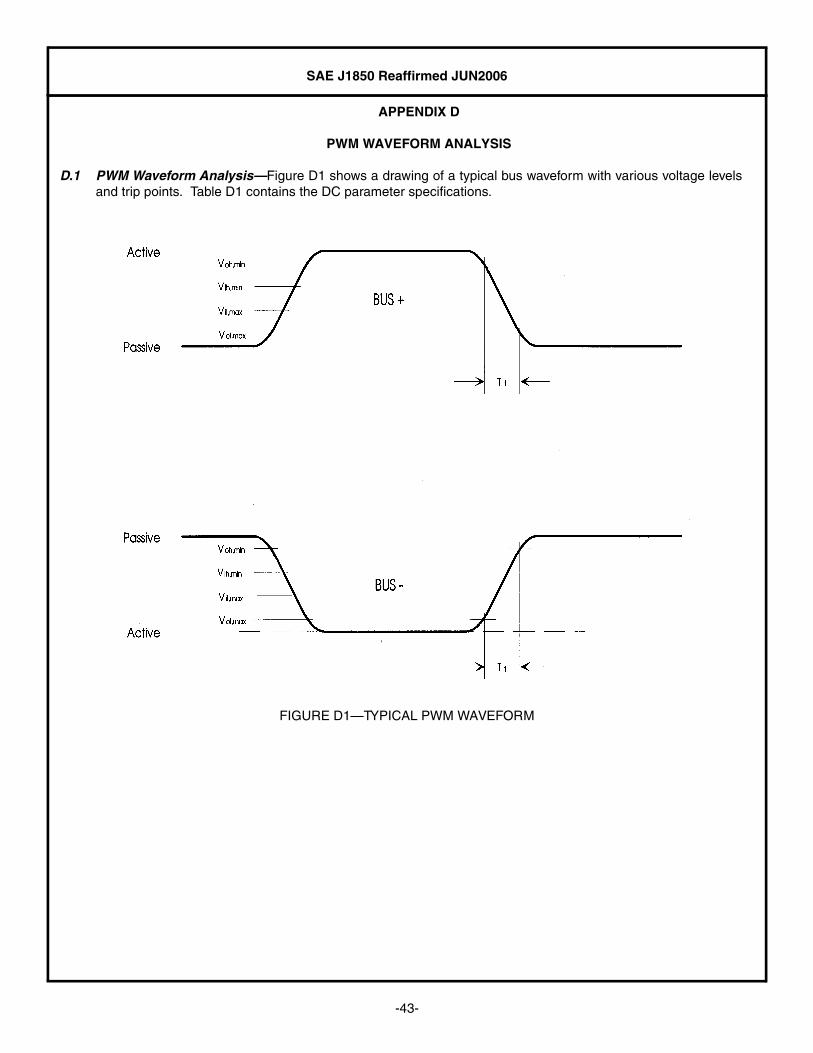
SAE J1850 Reaffirmed JUN2006
-43-
APPENDIX D
PWM WAVEFORM ANALYSIS
D.1 PWM Waveform Analysis—Figure D1 shows a drawing of a typical bus waveform with various voltage levelsand trip points. Table D1 contains the DC parameter specifications.
FIGURE D1—TYPICAL PWM WAVEFORM
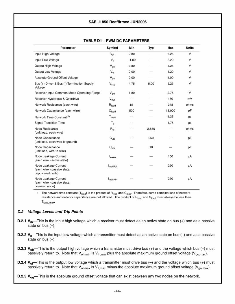
SAE J1850 Reaffirmed JUN2006
-44-
D.2 Voltage Levels and Trip Points
D.2.1 Vih—This is the input high voltage which a receiver must detect as an active state on bus (+) and as a passivestate on bus (–).
D.2.2 Vil—This is the input low voltage which a transmitter must detect as an active state on bus (–) and as a passivestate on bus (+).
D.2.3 Voh—This is the output high voltage which a transmitter must drive bus (+) and the voltage which bus (–) mustpassively return to. Note that Voh,min is Vih,min plus the absolute maximum ground offset voltage (Vgo,max).
D.2.4 Vol—This is the output low voltage which a transmitter must drive bus (–) and the voltage which bus (+) mustpassively return to. Note that Vol,max is Vil,max minus the absolute maximum ground offset voltage (Vgo,max).
D.2.5 Vog—This is the absolute ground offset voltage that can exist between any two nodes on the network.
TABLE D1—PWM DC PARAMETERS
Parameter Symbol Min Typ Max Units
Input High Voltage Vih 2.80 — 6.25 V
Input Low Voltage Vil –1.00 — 2.20 V
Output High Voltage Voh 3.80 — 5.25 V
Output Low Voltage Vol 0.00 — 1.20 V
Absolute Ground Offset Voltage Vgo 0.00 — 1.00 V
Bus (+) Driver & Bus (() Termination Supply Voltage
Vsup 4.75 5.00 5.25 V
Receiver Input Common Mode Operating Range Vcm 1.80 — 2.75 V
Receiver Hysteresis & Overdrive Vhys — — 180 mV
Network Resistance (each wire) Rload 85 — 378 ohms
Network Capacitance (each wire) Cload 500 — 15,000 pF
Network Time Constant(1)
1. The network time constant (Tload) is the product of Rload and Cload. Therefore, some combinations of network resistance and network capacitance are not allowed. The product of Rload and Gload must always be less than Tload, max.
Tload — — 1.35 µs
Signal Transition Time Tt — — 1.75 µs
Node Resistance(unit load, each wire)
Rul — 2,880 — ohms
Node Capacitance(unit load, each wire to ground)
Culg — 250 — pF
Node Capacitance(unit load, wire-to-wire)
Culw — 10 — pF
Node Leakage Current(each wire - active state)
IleakA — — 100 µA
Node Leakage Current(each wire - passive state,unpowered node)
IleakPU — — 250 µA
Node Leakage Current(each wire - passive state,powered node)
IleakPP — — 250 µA

SAE J1850 Reaffirmed JUN2006
-45-
D.2.6 Vsup—This is the supply voltage which a transmitter must use to drive bus (+) and terminate bus (–).
D.2.7 Vcm—This is the receiver input common mode operating range. In order for the differential receiver torecognize a valid signal transition, the bus (+) and bus (–) signals must cross at a voltage within this range.
D.2.8 Vhys—This is the receiver hysteresis and overdrive voltage including any power supply reference tolerance.
D.2.9 Rload—This is the equivalent network resistance from each bus wire to the corresponding passive voltagesource.
D.2.10 Cload—This is the equivalent network capacitance from each bus wire to ground.
D.2.11 Tload—This is the network time constant for each bus wire. This is the product of Rload and Cload of each buswire. The time constant determines the maximum active-to-passive transition time.
D.2.12 Tt—This is the signal transition time for each bus wire from either the active-to-passive state or passive-to-active state. The passive-to-active edge is driven by the transmitter and shall be no more than Tt,max. Theactive-to-passive edge is determined by the network time constant, bus voltage levels, and the passive statesupply voltage level.
D.2.13 Culg—This is the unit load node capacitance of each wire to ground. This capacitance, along with the unitload node capacitance wire-to-wire, results in the total network capacitance referred to in C.2.10.
D.2.14 Culw—This is the unit load node capacitance wire-to-wire. This capacitance along with the nodecapacitance of each wire to ground results in the total network capacitance referred to in C.2.10.
D.2.15 IleakA—This is the leakage current of each wire when the bus is in the active state.
D.2.16 IleakPU—This is the leakage current of each wire when the bus is in the passive state and the node isunpowered.
D.2.17 IleakPP—This is the leakage current of each wire when the bus is in the passive state and the node ispowered.
D.3 Input Voltage Limits—Given the Bus (+) Driver & Bus (–) Termination Supply Voltage (Vsup) and themaximum Receiver Hysteresis and Overdrive Voltage (Vhys), Vih and Vil can be derived. (See Equations D1through D4.)
(Eq. D1)
(Eq. D2)
(Eq. D3)
(Eq. D4)
where 1/2 the Vil,max and Vih,min assumes a receive comparator voltage level of one-half of the supply voltage.It turns out this is a good tradeoff for voltage ground offset capability versus output drive requirements.
D.4 Output Voltage Limits—Output voltage limits can be derived directly from the input voltage limits. (SeeEquations D5 through D8.)
(Eq. D5)
Vil min, Ground Reference( ) Vgo– 0.00 1.00– 1.00V–= = =
Vil max, 1 2 Vsup min,( )⁄ Vhys min,– 1 2 4.75( )⁄ 0.18– 2.20V= = =
Vih min, 1 2 Vsup max,( ) Vhys max,+⁄ 1 2 5.25( )⁄ 0.18+ 2.81V= = =
Vih max, Vsup max, Vgo+ 5.25 1.00+ 6.25V= = =
Vol min, Vil min, Vgo+ 1.00– 1.00+ 0V (Ground Reference)= = =

SAE J1850 Reaffirmed JUN2006
-46-
(Eq. D6)
(Eq. D7)
(Eq. D8)
D.5 D.5 Network Time Constant & Signal Transition Time—In order to guarantee signal cross over in theReceiver Input Common Mode Operating Range (Vcm) the signal transition time must be less than 2.20 ms.This is Tt,max + the worst case transition time from Vol,min to Vol,max for Bus (–), or Voh,max to Voh,min for Bus (+).Therefore, given Dt = 2.20 ms, the following relationship for Voh,min must be satisfied for Bus (–) and Vol,max forBus (+). (See Equations D9 through D12.)
(Eq. D9)
(Eq. D10)
From this, the maximum network time constant (Tload,max) can be derived.
(Eq. D11)
(Eq. D12)
Choosing a Tload,max of 1.35 ms satisfies both equations. Given a maximum network time constant of 1.35 ms,the signal transition time Tt,max can be found by subtracting the time from Vol,min to Vol,max (for Bus –) or thetime from Voh,max to Voh,min (for Bus +) from 2.20 ms. (See Equations D13 through D16.)
Bus (–):
(Eq. D13)
(Eq. D14)
Bus (+)
(Eq. D15)
(Eq. D16)
Therefore, choosing a network time constant Tload,max, of 1.35 ms and a signal transition time Tt,max of 1.75 msensures that the two bus signals will cross within the Common Mode Operating Range.
Vol max, Vil max, Vgo– 2.20 1.00– 1.20V= = =
Voh min, Vih min, Vgo+ 2.80 1.00+ 3.80V= = =
Voh max, Vih max, Vgo– 6.25 1.00– 5.25 Vsup max,( )= = =
Voh min, Vsup min, 1 e Dt Tload max,⁄( )––( ) for Bus )–(=
Vol max, Voh max, e Dt Tload max,⁄( )–( ) for Bus (+)=
Tload max, Bus ) –( ∆t In÷ 1 V( oh min, Vsup min,⁄ ) )–(–=
2.20– In 1 3.80 4.75⁄( )–( ) 1.37µs=÷=
Tload max, Bus+)( ∆t In÷ V( ol max, Voh max,⁄ ) )–=
2.20– In 1.20 5.25⁄( ) 1.49µs=÷=
T Vol min, to Vol max,( ) Tload max, In 1 Vol max, Vsup min,⁄( )–( )( )–=
1.35 In 1 1.20 4.75⁄( )–( )( ) 0.39µs=–=
Tload max, 2.20 T Vol min, to Vol max,( )–=
2.20 0.39 1.81µs=–=
T Voh max, to Voh min,( ) Tload max, In Voh min, Voh max,⁄( )( )–=
1.35 In 3.80 5.25⁄( )( ) 0.44µs=–=
Tload max, 2.20 T Voh max, to Voh min,( )–=
2.20 0.44 1.76µs=–=