circuits laboratory experiment 6 · pdf filecircuits laboratory experiment 6 transistor...
TRANSCRIPT
CIRCUITS LABORATORY
EXPERIMENT 6
TRANSISTOR CHARACTERISTICS
6.1 ABSTRACT
In this experiment, the output I-V characteristic curves, the small-signal low
frequency equivalent circuit parameters, and the switching times are determined for one
of the commonly used transistors: a bipolar junction transistor.
6.2 INTRODUCTION
The advent of the modern electronic and communication age began in late 1947
with the invention of the transistor. Rarely has any component of any apparatus received
the public attention and acclaim of this invention. Although everyone knows what a
transistor radio is, few know how it works or why the transistor itself is so important in
electronic systems. From an economic point-of-view its main advantages are small size,
low-cost, and high reliability. Basically, however, the importance of the transistor
derives from the fact that it is a three-terminal device that can provide amplification or
gain. The three terminals serve to isolate input and output, while gain allows for
conversion of dc power into signal power.
Two of the most important applications for the transistor are (1) as an amplifier in
analog electronic systems, and (2) as a switch in digital systems. In this experiment we
will examine some of the characteristics of transistors in these modes of operation. For
this purpose we will investigate one of the common transistors, the bipolar junction
transistor (BJT).
6 - 1
6.3 BIPOLAR JUNCTION TRANSISTOR (BJT)
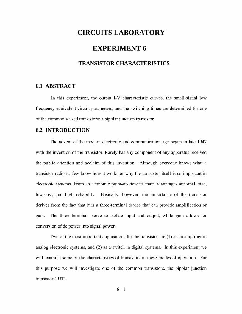
Figure 6.1: Symbols for BJTs.
6.3.1 Basic Concepts
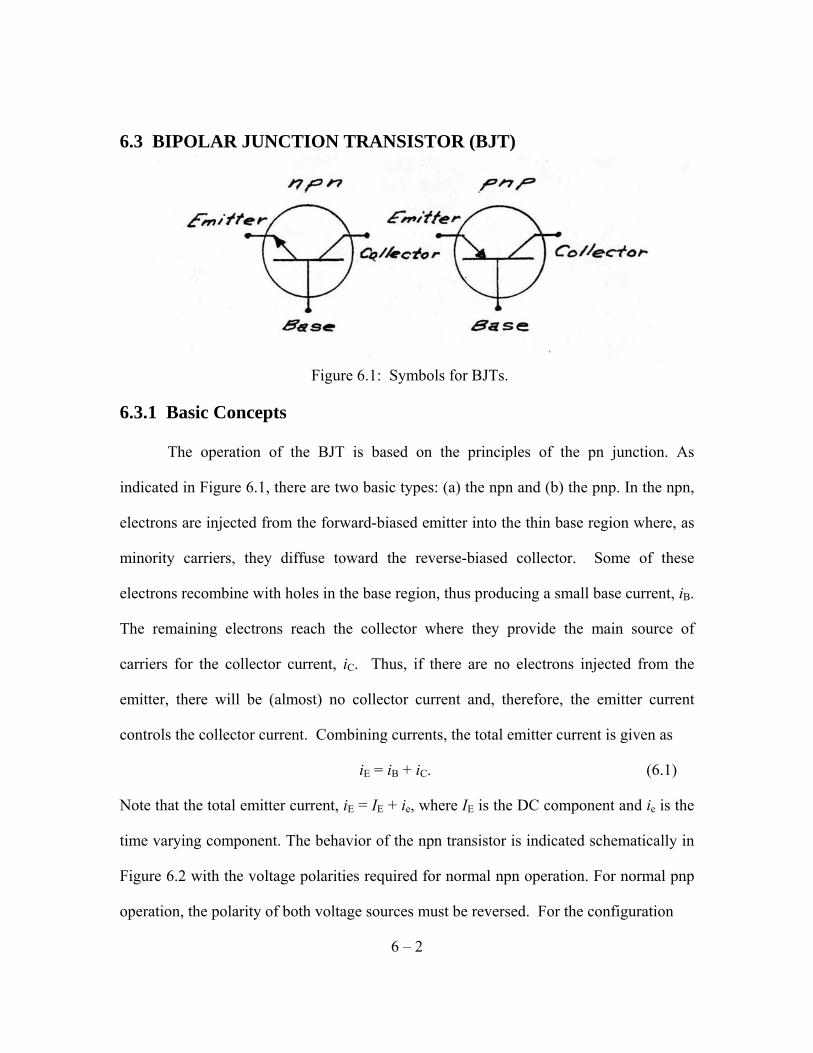
The operation of the BJT is based on the principles of the pn junction. As
indicated in Figure 6.1, there are two basic types: (a) the npn and (b) the pnp. In the npn,
electrons are injected from the forward-biased emitter into the thin base region where, as
minority carriers, they diffuse toward the reverse-biased collector. Some of these
electrons recombine with holes in the base region, thus producing a small base current, iB.
The remaining electrons reach the collector where they provide the main source of
carriers for the collector current, iC. Thus, if there are no electrons injected from the
emitter, there will be (almost) no collector current and, therefore, the emitter current
controls the collector current. Combining currents, the total emitter current is given as
iE = iB + iC. (6.1)
Note that the total emitter current, iE = IE + ie, where IE is the DC component and ie is the
time varying component. The behavior of the npn transistor is indicated schematically in
Figure 6.2 with the voltage polarities required for normal npn operation. For normal pnp
operation, the polarity of both voltage sources must be reversed. For the configuration
6 – 2
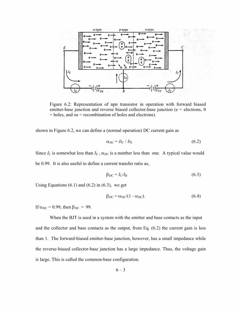
Figure 6.2: Representation of npn transistor in operation with forward biased emitter-base junction and reverse biased collector-base junction (e = electrons, 0 = holes, and oe = recombination of holes and electrons).
shown in Figure 6.2, we can define a (normal operation) DC current gain as
αDC = IiC / IiE (6.2)
Since IC is somewhat less than IE , αDC is a number less than one. A typical value would be 0.99. It is also useful to define a current transfer ratio as, βDC = IC/IB (6.3) Using Equations (6.1) and (6.2) in (6.3), we get βDC = αDC/(1 - αDC). (6.4) If αDC = 0.99, then βDC = 99. When the BJT is used in a system with the emitter and base contacts as the input and the collector and base contacts as the output, from Eq. (6.2) the current gain is less
than 1. The forward-biased emitter-base junction, however, has a small impedance while
the reverse-biased collector-base junction has a large impedance. Thus, the voltage gain
is large. This is called the common-base configuration.
6 – 3
.10 mAR
VIC
CCC ==
When the BJT is used with the base and emitter terminals as the input and the
collector and emitter terminals as the output, from Eq. (6.4) the current gain as well as the
voltage gain is large. It is for this reason that this common-emitter (CE) configuration is
the most useful connection for the BJT in electronic systems.
Figure 6. 3a: Cornmon-emitter Figure 6.3b: Collector characteristic connections for npn transistor. curves for the common- emitter connection of npn transistor.
This configuration is shown in Figure 6.3a with the output I-V characteristics indicated in
Figure 6.3b. Notice from the I-V characteristics that the output collector current is
controlled by the input base current as modeled in Equation. (6.3).
6.3.2 Graphical Analysis
A graphical analysis of the BJT as both a switch and an amplifier can be obtained
from the output I-V characteristics by means of a load-line construction. If we take Vcc =
10 volts and Rc = 1 kΩ in Figure 6.3a, then the load-line intercepts on the output
characteristic are VCE = 10 volts and
(6.5)
6 - 4
VCE
IBBase Current
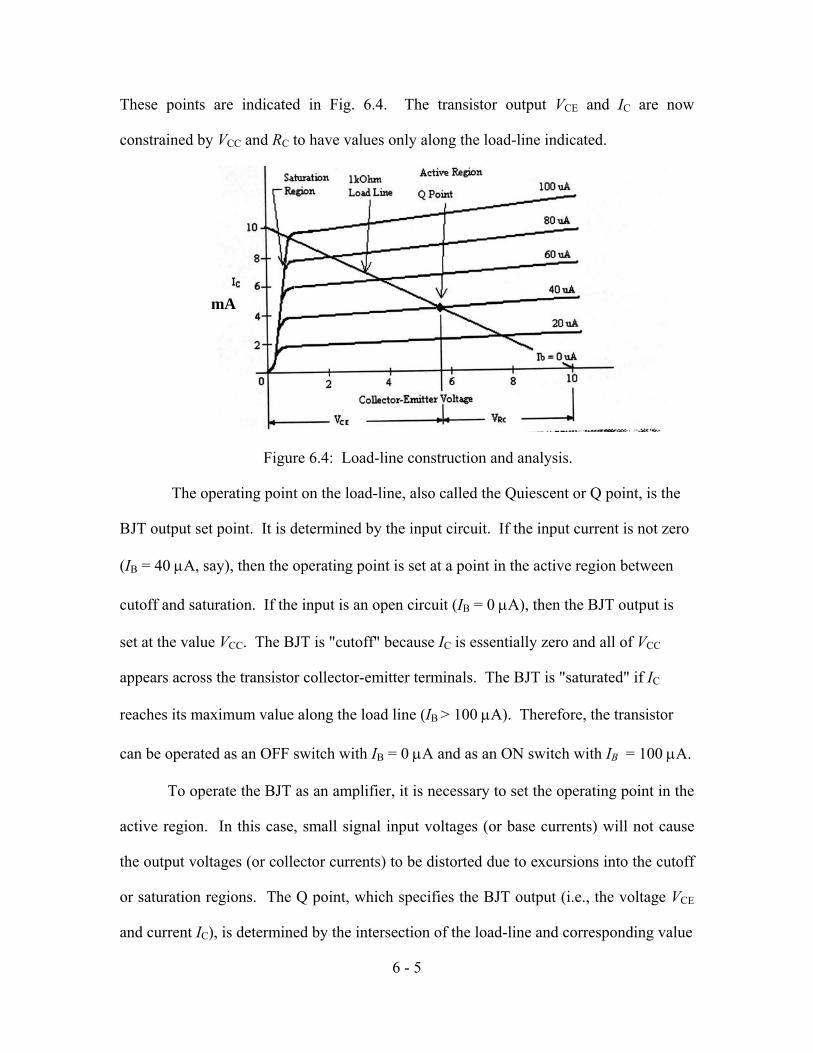
These points are indicated in Fig. 6.4. The transistor output VCE and IC are now
constrained by VCC and RC to have values only along the load-line indicated.
Figure 6.4: Load-line construction and analysis.
The operating point on the load-line, also called the Quiescent or Q point, is the
BJT output set point. It is determined by the input circuit. If the input current is not zero
(IB = 40 μA, say), then the operating point is set at a point in the active region between
cutoff and saturation. If the input is an open circuit (IB = 0 μA), then the BJT output is
set at the value VCC. The BJT is "cutoff" because IC is essentially zero and all of VCC
appears across the transistor collector-emitter terminals. The BJT is "saturated" if IC
reaches its maximum value along the load line (IB > 100 μA). Therefore, the transistor
can be operated as an OFF switch with IB = 0 μA and as an ON switch with IB = 100 μA.
To operate the BJT as an amplifier, it is necessary to set the operating point in the
active region. In this case, small signal input voltages (or base currents) will not cause
the output voltages (or collector currents) to be distorted due to excursions into the cutoff
or saturation regions. The Q point, which specifies the BJT output (i.e., the voltage VCE
and current IC), is determined by the intersection of the load-line and corresponding value
6 - 5
mA
of the base current IB. The value of IB is controlled by the input circuit (which is RB and
VBB in the CE configuration shown in Fig. 6.3(a)).
6.3.3 DC Equivalent Circuit
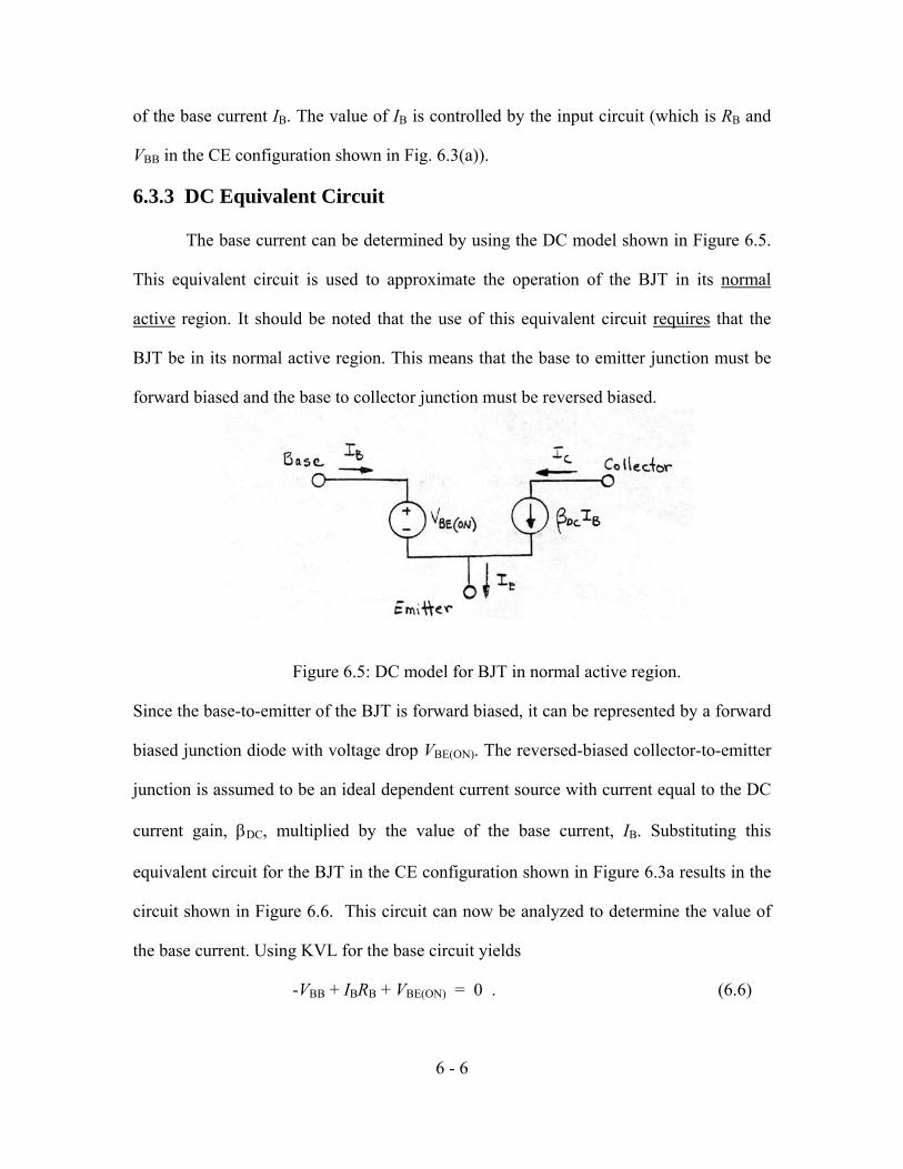
The base current can be determined by using the DC model shown in Figure 6.5.
This equivalent circuit is used to approximate the operation of the BJT in its normal
active region. It should be noted that the use of this equivalent circuit requires that the
BJT be in its normal active region. This means that the base to emitter junction must be
forward biased and the base to collector junction must be reversed biased.
Figure 6.5: DC model for BJT in normal active region.
Since the base-to-emitter of the BJT is forward biased, it can be represented by a forward
biased junction diode with voltage drop VBE(ON). The reversed-biased collector-to-emitter
junction is assumed to be an ideal dependent current source with current equal to the DC
current gain, βDC, multiplied by the value of the base current, IB. Substituting this
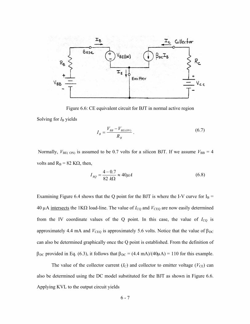
equivalent circuit for the BJT in the CE configuration shown in Figure 6.3a results in the
circuit shown in Figure 6.6. This circuit can now be analyzed to determine the value of
the base current. Using KVL for the base circuit yields
-VBB + IBRB + VBE(ON) = 0 . (6.6)
6 - 6
.)(
B
ONBEBBB R
VVI
−=
Ak
I BQ μ4082
7.04≈
Ω−
=
Figure 6.6: CE equivalent circuit for BJT in normal active region
Solving for IB yields
(6.7)
Normally, VBE( ON) is assumed to be 0.7 volts for a silicon BJT. If we assume VBB = 4
volts and RB = 82 KΩ, then,
(6.8)
Examining Figure 6.4 shows that the Q point for the BJT is where the I-V curve for IB =
40 μA intersects the 1KΩ load-line. The value of ICQ and VCEQ are now easily determined
from the IV coordinate values of the Q point. In this case, the value of ICQ is
approximately 4.4 mA and VCEQ is approximately 5.6 volts. Notice that the value of βDC
can also be determined graphically once the Q point is established. From the definition of
βDC provided in Eq. (6.3), it follows that βDC = (4.4 mA)/(40μA) = 110 for this example.
The value of the collector current (IC) and collector to emitter voltage (VCE) can
also be determined using the DC model substituted for the BJT as shown in Figure 6.6.
Applying KVL to the output circuit yields
6 - 7
C
CECCC R
VVI −=
-VCC + ICRC + VCE = 0 . (6.9)
Solving for IC gives
(6.10)
Solving for VCE gives
VCE = VCC - ICRC . (6.11)
From Eq. (6.3) we know that
IC = βDC IB . (6.12)
Substituting into Eq. (6.11) above gives
VCE = VCC - (βDC IB) RC . (6.13)
Continuing with our example, it follows that ICQ = (110) (40 μA) = 4.4 mA and VCEQ =
10 - (4.4) (1) = 5.6 V using the DC Model.
6.3.4 AC or Small Signal Equivalent Circuit
In order to analyze the operation of the BJT as an amplifier, an AC (or small
signal) equivalent circuit is utilized. A widely used small signal circuit model is called
the Hybrid-π model and is shown in Figure 6.7. Use of this small signal model assumes
the BJT is operating in its normal active region; that is, it is biased at a Q point in the
active region and provides an equivalent circuit for small changes in voltage and current
around the Q point.
6 - 8
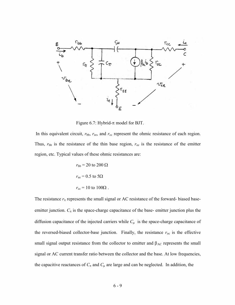
Figure 6.7: Hybrid-π model for BJT.
In this equivalent circuit, rbb, ree, and rcc represent the ohmic resistance of each region.
Thus, rbb is the resistance of the thin base region, ree is the resistance of the emitter
region, etc. Typical values of these ohmic resistances are:
rbb = 20 to 200 Ω
ree = 0.5 to 5Ω
rcc = 10 to 100Ω .
The resistance rπ represents the small signal or AC resistance of the forward- biased base-
ernitter junction. Cπ is the space-charge capacitance of the base- emitter junction plus the
diffusion capacitance of the injected carriers while Cμ is the space-charge capacitance of
the reversed-biased collector-base junction. Finally, the resistance roc is the effective
small signal output resistance from the collector to emitter and βAC represents the small
signal or AC current transfer ratio between the collector and the base. At low frequencies,
the capacitive reactances of Cπ and Cμ are large and can be neglected. In addition, the
6 - 9
B
BE
ivrΔΔ
=π vCE = const.
QC
TAC
IVr β
π =
values of the ohmic resistances, i.e., rbb, ree and rcc, can often be ignored. This results in
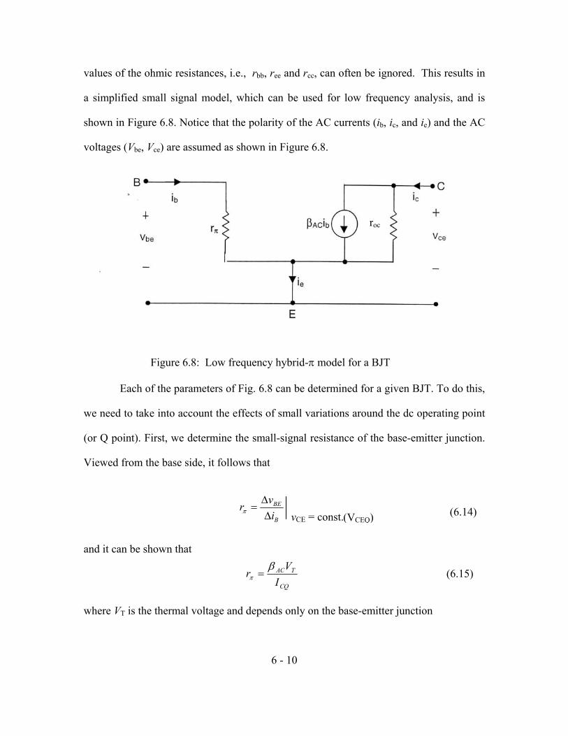
a simplified small signal model, which can be used for low frequency analysis, and is
shown in Figure 6.8. Notice that the polarity of the AC currents (ib, ic, and ie) and the AC
voltages (Vbe, Vce) are assumed as shown in Figure 6.8.
Figure 6.8: Low frequency hybrid-π model for a BJT
Each of the parameters of Fig. 6.8 can be determined for a given BJT. To do this,
we need to take into account the effects of small variations around the dc operating point
(or Q point). First, we determine the small-signal resistance of the base-emitter junction.
Viewed from the base side, it follows that
(6.14)
and it can be shown that (6.15) where VT is the thermal voltage and depends only on the base-emitter junction
6 - 10
roc
(VCEQ)
qkTVT =
.)26(
QC
AC
ImV
rβ
π =
temperature. VT is defined by
(6.16)
where k = Boltzmann's constant = 1.38x10⁻²³ J/K
T = absolute temperature, K = 273 + temperature in deg. C.
q = electron charge = 1.602x10⁻¹⁹ Coulomb
At normal room temperature, VT = 26 mV. Thus, at 27° C.,
(6.17)
Thus, rπ can be determined from the Q point, the junction temperature of the transistor,
and the value of βAC for the transistor.
From the small signal circuit model in Figure 6.8 we see that a small change in
current at the input to the transistor (i.e., the base current, ib) will result in a change of the
current at the output of the transistor (i.e., the collector current, ic). These two current
changes are related by the small signal current gain of the transistor, βAC. So,
ic = βAC ib + vce/rOC . (6.18)
The AC current gain can be determined by
(6.19)
Finally, the effective output resistance inherent in the transistor from the collector to the
emitter is determined as
IB = IBQ= const. (6.20)
6 - 11
B
CAC i
iΔΔ
=βVCE=VCEQ=const
C
CEOC i
vrΔΔ
=
Using the above and analyzing the characteristic curve and Q point from Figure 6.4
and
The operation of the CE amplifier shown in Figure 6.3a, as a result of applying a small
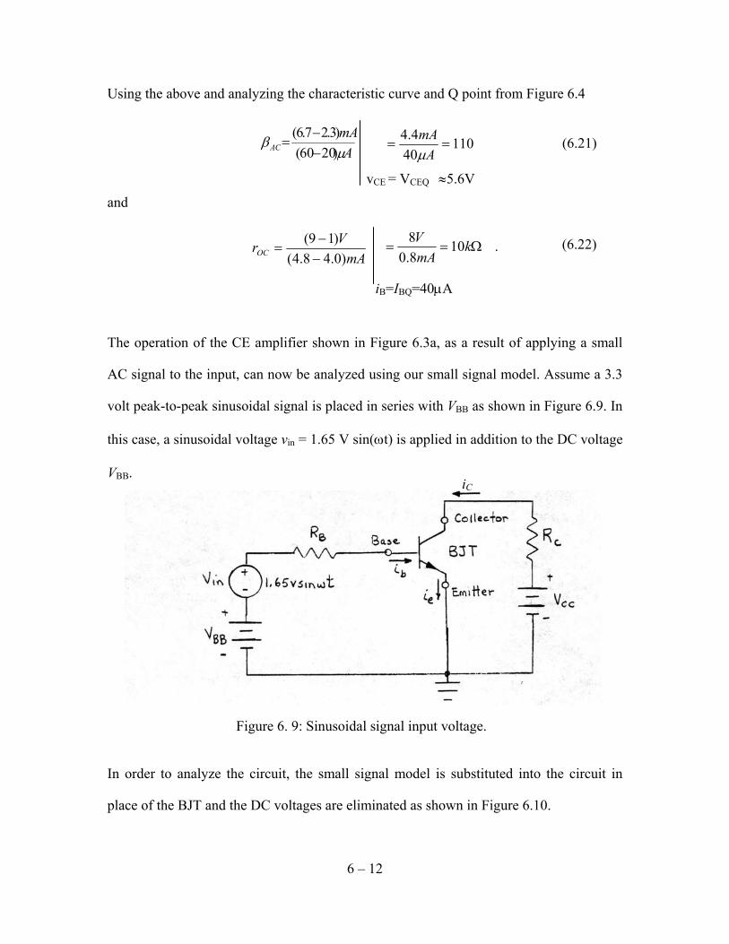
AC signal to the input, can now be analyzed using our small signal model. Assume a 3.3
volt peak-to-peak sinusoidal signal is placed in series with VBB as shown in Figure 6.9. In
this case, a sinusoidal voltage vin = 1.65 V sin(ωt) is applied in addition to the DC voltage
VBB.
Figure 6. 9: Sinusoidal signal input voltage. In order to analyze the circuit, the small signal model is substituted into the circuit in
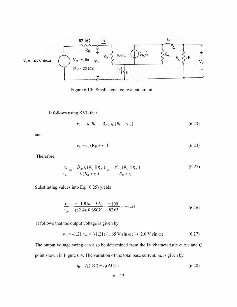
place of the BJT and the DC voltages are eliminated as shown in Figure 6.10.
6 – 12
mAVrOC )0.48.4(
)19(−−
=
iB=IBQ=40μA
.108.08
Ω== kmAV (6.22)
iC
AmA
AC μβ
)2060()3.27.6(
−−
=
vCE = VCEQ ≈5.6V
11040
4.4==
AmAμ
(6.21)
.)||()(
)||(0
ππ
ββrR
rRrRi
rRivv
B
OCCAC
Bb
OCCbAC
in +−
=+
−=
It follows using KVL that
v0 = -iC RC = -βAC ib (RC || rOC) (6.23)
and
vin = ib (RB + rπ ) (6.24)
Therefore,
(6.25)
Substituting values into Eq. (6.25) yields
(6.26)
It follows that the output voltage is given by v0 = -1.21 vin = (-1.21) (1.65 V sin ωt ) ≈ 2.0 V sin ωt . (6.27)
The output voltage swing can also be determined from the IV characteristic curve and Q
point shown in Figure 6.4. The variation of the total base current, iB, is given by
iB = IB(DC) + ib(AC) . (6.28)
6 – 13
.21.165.82
.100)650. 0 82 ( )10|| 1 ( 110 0 − ≈ − =
+ −
= k k kk
v v
in
650 Ω
o
Vs = 1.65 V sinωt Vin =vs for
(Rs<< 82 kΩ)
Figure 6.10: Small signal equivalent circuit
vbe
82 kΩ
We have already determined that IB(DC)) = IBQ = 40μA from the Q point. The AC
component of the base current is given by
(6.29)
It follows that the base current changes ± 20μA (or 40μA peak-to-peak). Thus, during the
positive half cycle, the base current changes from 40μA to 60μA and during the negative
halt cycle, it changes from 40μA to 20μA. Plotting this change on Figure 6.4 and moving
along the 1 KΩ load-line results in a value of iC ≈ 6.4mA for iB = 60μA and ic ≈ 2.4mA
for iB = 20μA. Thus, V0 = Vce changes from approximately 3.7V to 7.5V which represents
a 3.8 V peak-to-peak voltage output or Vo = -1.9V sin ωt where the minus sign
represents the 180° phase shift between the input and output voltages.
6.3.5 Switching Times
The transistor switch cannot respond instantaneously to a turn-on or a turn-off signal. In
many applications, it is important to be aware of the magnitude of possible errors caused
by a time delay in the switching circuit and how to minimize the time lags. In Figure
6.11, the response of a transistor switching circuit is shown when a turn-on and turn-off
signal VB is applied to the input circuit.
6 – 14
Atk
tVr R
v ACi
B in
b μ ω ω
π sin20
65.82sin65.1
)( ) ( ≈ =
+ =
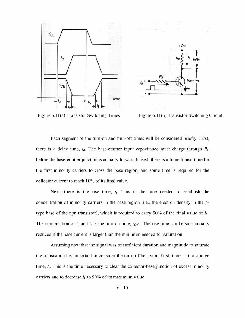
Each segment of the turn-on and turn-off times will be considered briefly. First,
there is a delay time, td. The base-emitter input capacitance must charge through RB
before the base-emitter junction is actually forward biased; there is a finite transit time for
the first minority carriers to cross the base region; and some time is required for the
collector current to reach 10% of its final value.
Next, there is the rise time, tr. This is the time needed to establish the
concentration of minority carriers in the base region (i.e., the electron density in the p-
type base of the npn transistor), which is required to carry 90% of the final value of IC.
The combination of td and tr is the turn-on time, tON . The rise time can be substantially
reduced if the base current is larger than the minimum needed for saturation.
Assuming now that the signal was of sufficient duration and magnitude to saturate
the transistor, it is important to consider the turn-off behavior. First, there is the storage
time, ts. This is the time necessary to clear the collector-base junction of excess minority
carriers and to decrease IC to 90% of its maximum value.
6 - 15
Figure 6.11(a) Transistor Switching Times Figure 6.11(b) Transistor Switching Circuit
The fall time, tf, is the time required for the output current to fall from 90% to
10% of its maximum value, and depends on the time required to discharge the collector-
emitter capacitance and the time required for the minority carriers in the base to be
collected. The combination of ts and tf is the turn-off time tOFF. These switching times are
usually measured by comparing VCE to VB on a dual-trace oscilloscope. Depending upon
the transistor and the measurement apparatus, it may not be possible to determine all four
switching times individually.
6.4 EXPERIMENTAL PROCEDURE
6.4.1 BJT Curve Tracer Analysis
You will be provided with a npn BJT and should first produce a copy of the transistor's
characteristics using the Tektronix 571 Curve Tracer. Your laboratory instructor will
provide an overview regarding the operation and settings to use on the curve tracer.
(a) With an RC and VCC as specified by your laboratory instructor, and a grounded
emitter, draw the corresponding load-line on your copy of the transistor's
characteristic curve. Determine and record an appropriate "Q" point along the load-
line for "midpoint biasing" that is a good approximation for operation as a minimum
distortion amplifier. Specify ICQ, VCEQ, and IBQ for your Q point. (Note: IBQ is
determined by multiplying the base current per step indication by the number of
steps you count from cutoff to the desired Q point using interpolation for the
distance between two base steps.)
(b) Determine and record βDC, βAC, and rOC using graphical techniques and Equations
(6.3), (6.19) and (6.20), respectively.
6 - 16
(c) Finally, determine and record the value of iB required to switch the BJT from cutoff
to saturation along the load-line determined in (a) above.
6.4.2 BJT DC Bias Model and Measurements
Measurements of the DC bias characteristics can best be made using the circuit
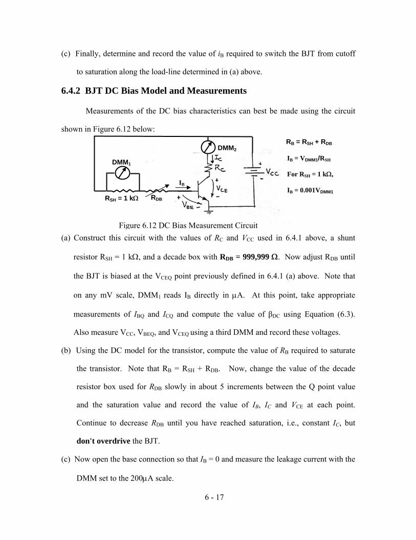
shown in Figure 6.12 below:
(a) Construct this circuit with the values of RC and VCC used in 6.4.1 above, a shunt
resistor RSH = 1 kΩ, and a decade box with RDB = 999,999 Ω. Now adjust RDB until
the BJT is biased at the VCEQ point previously defined in 6.4.1 (a) above. Note that
on any mV scale, DMM1 reads IB directly in μA. At this point, take appropriate
measurements of IBQ and ICQ and compute the value of βDC using Equation (6.3).
Also measure VCC, VBEQ, and VCEQ using a third DMM and record these voltages.
(b) Using the DC model for the transistor, compute the value of RB required to saturate
the transistor. Note that RB = RSH + RDB. Now, change the value of the decade
resistor box used for RDB slowly in about 5 increments between the Q point value
and the saturation value and record the value of IB, IC and VCE at each point.
Continue to decrease RDB until you have reached saturation, i.e., constant IC, but
don't overdrive the BJT.
(c) Now open the base connection so that IB = 0 and measure the leakage current with the
DMM set to the 200μA scale.
6 - 17
Figure 6.12 DC Bias Measurement Circuit
DMM2
DMM1
IB
RDB RSH = 1 kΩ
RB = RSH + RDB
IB = VDMM1/RSH
For RSH = 1 kΩ,
IB = 0.001VDMM1
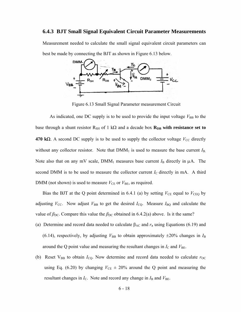
6.4.3 BJT Small Signal Equivalent Circuit Parameter Measurements
Measurement needed to calculate the small signal equivalent circuit parameters can
best be made by connecting the BJT as shown in Figure 6.13 below.
As indicated, one DC supply is to be used to provide the input voltage VBB to the
base through a shunt resistor RSH of 1 kΩ and a decade box RDB with resistance set to
470 kΩ. A second DC supply is to be used to supply the collector voltage VCC directly
without any collector resistor. Note that DMM1 is used to measure the base current IB.
Note also that on any mV scale, DMM1 measures base current IB directly in μA. The
second DMM is to be used to measure the collector current IC directly in mA. A third
DMM (not shown) is used to measure VCE or VBE, as required.
Bias the BJT at the Q point determined in 6.4.1 (a) by setting VCE equal to VCEQ by
adjusting VCC. Now adjust VBB to get the desired ICQ. Measure IBQ and calculate the
value of βDC. Compare this value the βDC obtained in 6.4.2(a) above. Is it the same?
(a) Determine and record data needed to calculate βAC and rπ using Equations (6.19) and
(6.14), respectively, by adjusting VBB to obtain approximately ±20% changes in IB
around the Q point value and measuring the resultant changes in IC and VBE.
(b) Reset VBB to obtain ICQ. Now determine and record data needed to calculate rOC
using Eq. (6.20) by changing VCE ± 20% around the Q point and measuring the
resultant changes in IC. Note and record any change in IB and VBE.
6 - 18
Figure 6.13 Small Signal Parameter measurement Circuit
RDB DMM2
DMM1
RSH
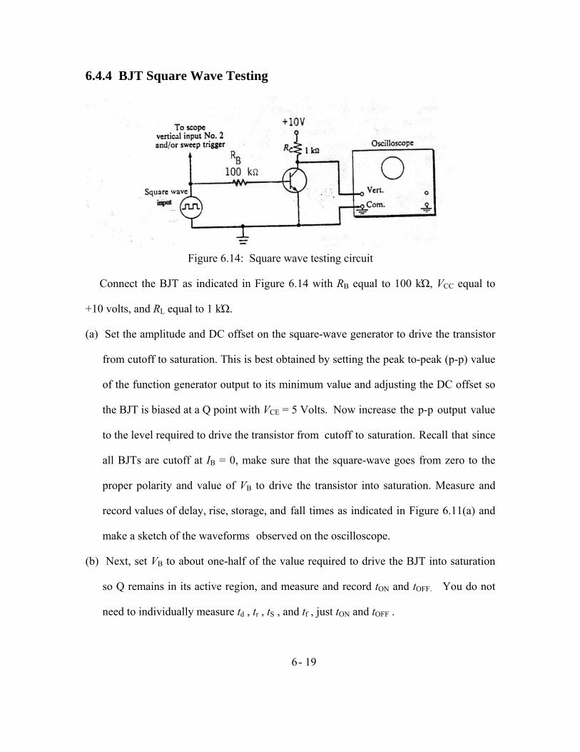
6.4.4 BJT Square Wave Testing
Figure 6.14: Square wave testing circuit
Connect the BJT as indicated in Figure 6.14 with RB equal to 100 kΏ, VCC equal to
+10 volts, and RL equal to 1 kΏ.
(a) Set the amplitude and DC offset on the square-wave generator to drive the transistor
from cutoff to saturation. This is best obtained by setting the peak to-peak (p-p) value
of the function generator output to its minimum value and adjusting the DC offset so
the BJT is biased at a Q point with VCE = 5 Volts. Now increase the p-p output value
to the level required to drive the transistor from cutoff to saturation. Recall that since
all BJTs are cutoff at IB = 0, make sure that the square-wave goes from zero to the
proper polarity and value of VB to drive the transistor into saturation. Measure and
record values of delay, rise, storage, and fall times as indicated in Figure 6.11(a) and
make a sketch of the waveforms observed on the oscilloscope.
(b) Next, set VB to about one-half of the value required to drive the BJT into saturation
so Q remains in its active region, and measure and record tON and tOFF. You do not
need to individually measure td , tr , tS , and tf , just tON and tOFF .
6 - 19
6.5 REPORT
6.5.1 Attach your transistor characteristics showing construction of the load-line per
6.4.1 (a) and the Q point. Identify the values for IBQ, VCEQ, and ICQ.
6.5.2 Show your work in determining βDC, βAC, and roc per 6.4.1 (b). Per 6.4.1 (c),
indicate the value of IB, obtained from the characteristic curve, that is needed to
saturate the BJT . Also, compute the value of rπ using Equation (6.15).
6.5.3 Using your measurements from 6.4.2(a), determine the values of IBQ, ICQ, and
βDC. Compare these to those obtained from the characteristic curve in 6.4.1 (b).
6.5.4 Show your computations of the value of RB required to drive the BJT to the
edge of saturation in 6.4.2(b). Make a table illustrating the measurements of VCE and
IC as the value of RB is decreased from the Q point value to the saturation value.
6.5.5 Describe the measurements you made and the value obtained for the leakage
current in 6.4.2(c).
6.5.6 Using the measurements from 6.4.3, determine the values of βAC, rπ, and roc.
Compare the value of βAC and roc with the values obtained from the characteristic
curve in 6.4.1 (b). Finally, compare the value of rπ obtained using the measurements
to that obtained using Eq. (6.15).
6.5.7 Insert your measured parameters for the BJT into Figure 6.10 and determine
the small signal output voltage across the 1 kΩ resistor for a 2 mV peak-to-peak
sinusoidal input voltage, i.e., Vin = 1 mV sin(ωt).
6.5.8 Sketch the waveform observed on the oscilloscope when the BJT is driven into
saturation and cutoff and indicate td, tr, ts, and tf, respectively. What is tON and tOFF
for this case? What is tON and tOFF when Q remains in its active region? Compare
these values to the previous values.
6 – 20
6.5.9 Design problem:
There is a need for a test fixture at in the Electrical Laboratory at WU for testing
2N2222A npn transistors for adequate current gain. Specifications are:
βDC ≥ 150 for
IBQ = 25μA and
VCEQ ≤ 5 Volts.
The transistor is to be accepted if it meets the above criteria; rejected if it fails.
Using only one DC power supply and whatever resistors, lamps, relays, and
auxiliary transistors you may need, design the electrical circuit needed to provide a
"go - no go" test for high gain npn transistors. To simplify matters, assume that
relays are available with operating coils that have high resistance and, therefore,
draw negligible current and that pull-in of the relay contacts occurs when the voltage
across the coil ≥ 5 Volts DC. Also, assume that green and red light emitting diodes
(IF = 10 mA & VF = 1.5 V) are available for use as "go" (green) and "no go" (red)
indicators.
Document your design as follows:
6.5.9.1 Briefly describe your design process,
6.5.9.2 Provide a circuit diagram for the transistor test circuit,
6.5.9.3 Define all component values needed for the test circuit.
6 - 21
6.6 REFERENCES
6.1 Sedra, Adel S. and Smith, Kenneth C., Microelectronic Circuits, 5th Edition,
Oxford University Press, New York, 2004
6.2 Ben G. Streetman, Solid State Electronic Devices, 2nd Ed. (Prentice-Hall,
Englewood Cliffs, NJ, 1980).
6.3 Adir Bar-Lev, Semiconductors and Electronic Devices, 2nd Ed. (Prentice-
Hall, Englewood Cliffs, NJ, 1984)
6.4 Maimstedt, H. V., Enke, C. G., Crouch, S. R., Control of Electrical
Ouantities In Instrumentation, (Benjamin, Menlo Park, NJ, 1973).
6.5 Sifferien, T. P., and Vartanian, V., Digital Electronics, (Prentice-Hall,
Englewood Cliffs, NJ, 1970).
6 - 22