circuits and active antennas for ultra- … in electromagnetics research b, vol. 23, 251{272, 2010...
TRANSCRIPT
Progress In Electromagnetics Research B, Vol. 23, 251–272, 2010
CIRCUITS AND ACTIVE ANTENNAS FOR ULTRA-WIDE BAND PULSE GENERATION AND TRANSMIS-SION
M. Kumar, A. Basu, and S. K. Koul
Centre for Applied Research in Electronics (CARE)Indian Institute of TechnologyDelhi, Hauz Khas, New Delhi-110016, India
Abstract—In this paper, the design and development of a novel activeantenna including circuits for Ultra-wide band (UWB) pulse generationand transmission have been described. In this design a pulse withpulse-width approximately 150 ps and amplitude 500 mV (peak-to-peak) was generated using a single high electron mobility transistor(HEMT) as the active device (and an optional Schottky diode forenhanced performance), this being the simplest circuit for generatingUWB pulses as far as we know. This circuit was integrated with anewly designed UWB planar microstrip-fed slot antenna, which is anactive antenna in the sense that in addition to radiating the signal, italso acts as a filter, which tailors the spectrum of the transmitted pulseto a shape close to that recommended for UWB communications. Wehave also given a quantitative analysis, which explains the operationof the circuit.
1. INTRODUCTION
It is well known that the UWB communication system is a fast-emerging technology with unique attractive features promising majoradvances in wireless communications, networking, radar, imaging, andpositioning systems.
UWB systems differ significantly from other wireless communica-tion standards. In the best-known embodiment, this communicatesusing a series of narrow un-modulated pulses instead of using a high-frequency carrier. The pulse can be seen as a burst of RF energy whereeach pulse carries one symbol of information. UWB systems obviously
Received 21 May 2010, Accepted 16 July 2010, Scheduled 25 July 2010Corresponding author: A. Basu (ananjan [email protected]).
252 Kumar, Basu, and Koul
cover a large spectrum, and unless properly handled, will interfere withexisting users. In order to keep this interference to a minimum, theFCC-USA and other regulatory groups have specified spectral masksfor different applications which show the allowed power output forspecific frequencies [1, 2]. For the most commonly used UWB commu-nication standard a large continuous bandwidth of 7.5 GHz is availablebetween 3.1GHz to 10.6 GHz at a maximum equivalent isotropic ra-diated power output of −41.3 dBm/MHz. Both the traditional pulse-based systems transmitting narrow pulses, which entirely or partiallyoccupy the UWB bandwidth, and the systems based on orthogonalfrequency-division multiplexing (OFDM) and similar techniques witha collection of narrowband carriers of at least 500MHz can utilize theUWB spectrum under the FCC’s rules.
One of the challenges for the implementation of UWB systemsis the development of a suitable antenna. Many UWB antennaswhich are compact, planar and low-cost have been proposed [3–8].Also ‘active antenna’ has been a growing area of research in recentyears as microwave integrated circuit and monolithic microwave circuittechnologies have become more mature allowing for higher levels ofintegration. The term ‘active antenna’ is too new to have a universallyaccepted definition; here it is used for a circuit which not onlyintegrates the active microwave circuits and the radiating elementon the same substrate, thereby reducing transition and transmissionlosses, but also utilizes the antenna for carrying out some circuitfunction (such as resonating or impedance-matching) apart fromradiating or receiving radiation. Following this definition, it can beobserved that while many active antennas have been demonstrated (forexample [9]) none have been proposed for UWB systems. The circuitproposed in [6] uses the term ‘active antenna’ somewhat differently anddoes not describe any additional circuit functionality in the antenna.Here, the development of an antenna which carries out pulse-shapingin order to match the prescribed spectrum for UWB pulses will bedescribed.
Numerous ultra-wideband, ultra-short-pulse transmitters havebeen developed — for example [10]. Most of these circuits arequite sophisticated, employing high-performance components and sub-systems. The simplest circuit that has been described is in [11] and thisalso has used a step-recovery diode, which is a component incompatiblewith most MMIC/RFIC processes. In this paper, a new scheme forUWB pulse generation is proposed. To the best of our knowledge,this is the simplest circuit proposed for generating UWB pulses from adigital input, employing one FET, one optional diode and a few passivecomponents. It can be implemented in MIC (employing distributed
Progress In Electromagnetics Research B, Vol. 23, 2010 253
approximations for L and C) or MMIC, and some extended form ofCMOS-RF such as BiCMOS (if diode is required).
This paper is divided into four sections, the first one presenting anintroduction and the scope of the paper. Section 2 presents a detailedaccount of UWB signal generation circuits starting from validation atlow frequencies. A novel and simple method to generate UWB pulsesusing a BJT or a HEMT/MESFET is described, and a quantitativeanalysis to explain the principle of action is given. Experimentalwork to validate the simulated results at microwave frequencies (3–10GHz) is presented in Section 3. Section 4 describes the UWB signaltransmitter circuit incorporating an active antenna.
2. UWB SIGNAL GENERATION CIRCUIT
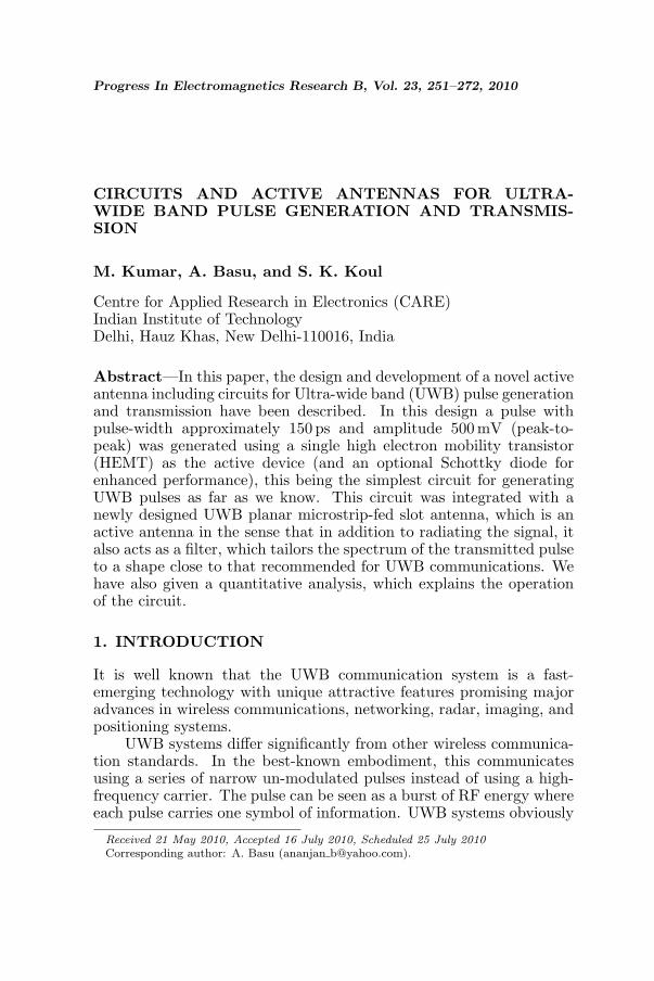
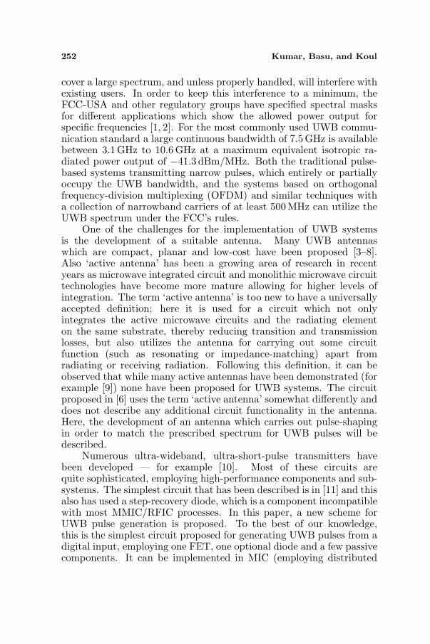
UWB signals have been usually generated using two techniques. Oneis to generate a narrow pulse using a differentiator-type circuit, andthen modify the shape by filters [12] or an up-converter [13] to fit theFCC spectral mask. The other way is to generate a precise UWB pulsewhose frequency spectrum satisfies the FCC regulation [14, 15]. Highperformance circuits following both approaches have been reported,but these have all been quite complex. In any case, the block diagramwhich describes the process is shown in Fig. 1. This is applicable tothe circuits presented in this paper as well. The direct implementationof the first approach shown in Fig. 2 however leads to pulse-shapesare quite sensitive to rise and fall time. This is intuitively expected,and was verified using simple circuit simulation. More importantly,this approach produces pulses at both rising and falling edges of theinput, and fairly complicated circuitry has to be used to eliminate oneof them.
A new scheme is proposed for the generation of short pulse using aFET (use of a BJT is also possible) as an active device which overcomesthese problems. These circuits are described next. We mention herethat all simulations were done on Agilent ADS software.
Circuits
Digital Information
(upto 500 MBbps)UWB Pulses
Circuits
Figure 1. Generalized schematic for generation of UWB pulses.
254 Kumar, Basu, and Koul
DifferentiatorSimple Filter/ Wave shaping
Networks
Pulse TrainUWB Pulses
DifferentiatorSimple Filter/ Wave shaping
Networks
Figure 2. A simple implementation of UWB pulse generation scheme.
50 1nF50
Bit Sequence
2.5V
Vout
Vin Vg
1 µF
800 nH
ΩΩ
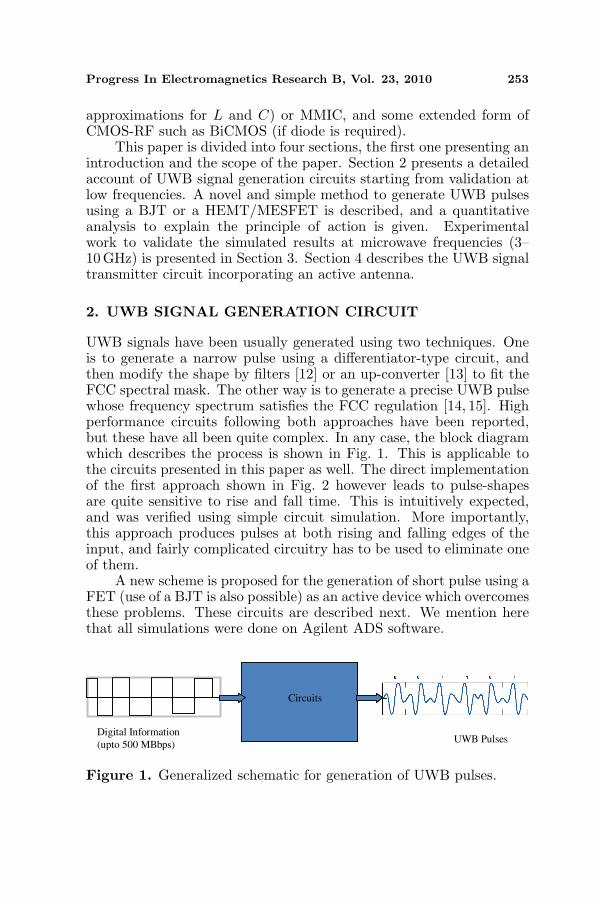
Figure 3. Basic short-pulse generation circuit at low frequency.
50 100 150 200 250 300 350 400 4500 500
-2.0
-1.5
-1.0
-0.5
-2.5
0.0
time, usec
Vin
, V
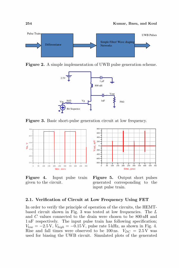
Figure 4. Input pulse traingiven to the circuit.
50 100 150 200 250 300 350 400 4500 500
600
400
200
0
200
400
600
800
800
time, µsec
Vout,
mV
-
-
-
-
Figure 5. Output short pulsesgenerated corresponding to theinput pulse train.
2.1. Verification of Circuit at Low Frequency Using FET
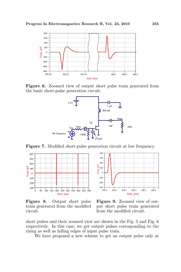
In order to verify the principle of operation of the circuits, the HEMT-based circuit shown in Fig. 3 was tested at low frequencies. The Land C values connected to the drain were chosen to be 800 nH and1 nF respectively. The input pulse train has following specification;Vlow = −2.5V, Vhigh = −0.15V, pulse rate 5 kHz, as shown in Fig. 4.Rise and fall times were observed to be 100 ns. VDC = 2.5V wasused for biasing the UWB circuit. Simulated plots of the generated
Progress In Electromagnetics Research B, Vol. 23, 2010 255
300.12 300.34299.90
-600
-400
-200
0
200
400
600
-800
800
time, usec
Vo
ut,
mV
400.1 400.3 400.5
Figure 6. Zoomed view of output short pulse train generated fromthe basic short-pulse generation circuit.
50 1nF50
Bit Sequence
2.5V
Vout
Vin
Vg
1 µF
800 nH
100K
470 pF
Vout
ΩΩ
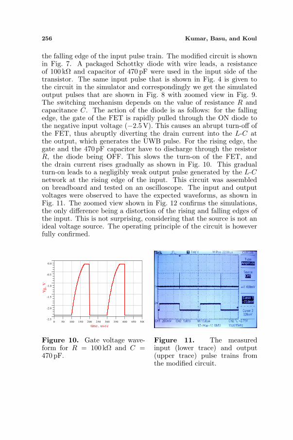
Figure 7. Modified short-pulse generation circuit at low frequency.
50 100 150 200 250 300 350 400 4500 500
-200
-100
0
100
200
300
-300
400
time, µsec
Vout,
mV
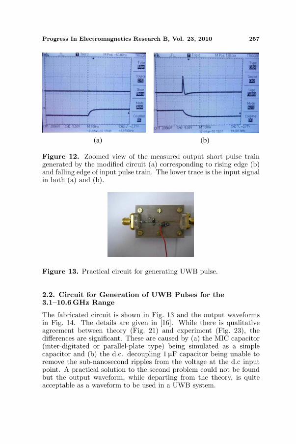
Figure 8. Output short pulsetrain generated from the modifiedcircuit.
400.1 400.3 400.5 400.7399.9 400.9
-200
-100
0
100
200
300
-300
400
time, µsec
Vout,
mV
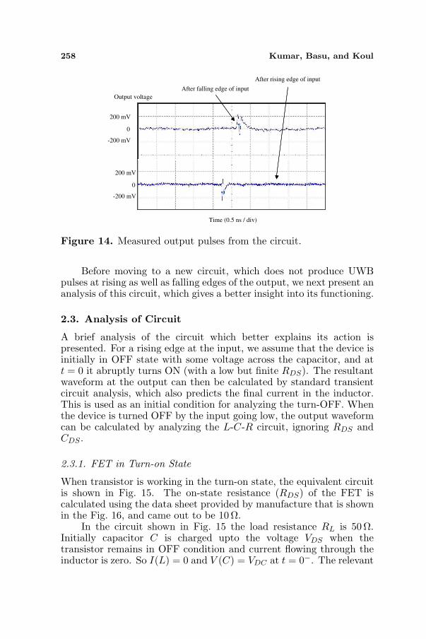
Figure 9. Zoomed view of out-put short pulse train generatedfrom the modified circuit.
short pulses and their zoomed view are shown in the Fig. 5 and Fig. 6respectively. In this case, we get output pulses corresponding to therising as well as falling edges of input pulse train.
We have proposed a new scheme to get an output pulse only at
256 Kumar, Basu, and Koul
the falling edge of the input pulse train. The modified circuit is shownin Fig. 7. A packaged Schottky diode with wire leads, a resistanceof 100 kΩ and capacitor of 470 pF were used in the input side of thetransistor. The same input pulse that is shown in Fig. 4 is given tothe circuit in the simulator and correspondingly we get the simulatedoutput pulses that are shown in Fig. 8 with zoomed view in Fig. 9.The switching mechanism depends on the value of resistance R andcapacitance C. The action of the diode is as follows: for the fallingedge, the gate of the FET is rapidly pulled through the ON diode tothe negative input voltage (−2.5V). This causes an abrupt turn-off ofthe FET, thus abruptly diverting the drain current into the L-C atthe output, which generates the UWB pulse. For the rising edge, thegate and the 470 pF capacitor have to discharge through the resistorR, the diode being OFF. This slows the turn-on of the FET, andthe drain current rises gradually as shown in Fig. 10. This gradualturn-on leads to a negligibly weak output pulse generated by the L-Cnetwork at the rising edge of the input. This circuit was assembledon breadboard and tested on an oscilloscope. The input and outputvoltages were observed to have the expected waveforms, as shown inFig. 11. The zoomed view shown in Fig. 12 confirms the simulations,the only difference being a distortion of the rising and falling edges ofthe input. This is not surprising, considering that the source is not anideal voltage source. The operating principle of the circuit is howeverfully confirmed.
50 100 150 200 250 300 350 400 4500 500
-2.0
-1.5
-1.0
-0.5
-2.5
0.0
time, usec
Vg
, V
Figure 10. Gate voltage wave-form for R = 100 kΩ and C =470 pF.
Figure 11. The measuredinput (lower trace) and output(upper trace) pulse trains fromthe modified circuit.
Progress In Electromagnetics Research B, Vol. 23, 2010 257
(a) (b)
Figure 12. Zoomed view of the measured output short pulse traingenerated by the modified circuit (a) corresponding to rising edge (b)and falling edge of input pulse train. The lower trace is the input signalin both (a) and (b).
Figure 13. Practical circuit for generating UWB pulse.
2.2. Circuit for Generation of UWB Pulses for the3.1–10.6GHz Range
The fabricated circuit is shown in Fig. 13 and the output waveformsin Fig. 14. The details are given in [16]. While there is qualitativeagreement between theory (Fig. 21) and experiment (Fig. 23), thedifferences are significant. These are caused by (a) the MIC capacitor(inter-digitated or parallel-plate type) being simulated as a simplecapacitor and (b) the d.c. decoupling 1µF capacitor being unable toremove the sub-nanosecond ripples from the voltage at the d.c inputpoint. A practical solution to the second problem could not be foundbut the output waveform, while departing from the theory, is quiteacceptable as a waveform to be used in a UWB system.
258 Kumar, Basu, and Koul
Time (0.5 ns / div)
0
200 mV
-200 mV
0
200 mV
-200 mV
Output voltage
After falling edge of input
After rising edge of input
Figure 14. Measured output pulses from the circuit.
Before moving to a new circuit, which does not produce UWBpulses at rising as well as falling edges of the output, we next present ananalysis of this circuit, which gives a better insight into its functioning.
2.3. Analysis of Circuit
A brief analysis of the circuit which better explains its action ispresented. For a rising edge at the input, we assume that the device isinitially in OFF state with some voltage across the capacitor, and att = 0 it abruptly turns ON (with a low but finite RDS). The resultantwaveform at the output can then be calculated by standard transientcircuit analysis, which also predicts the final current in the inductor.This is used as an initial condition for analyzing the turn-OFF. Whenthe device is turned OFF by the input going low, the output waveformcan be calculated by analyzing the L-C-R circuit, ignoring RDS andCDS .
2.3.1. FET in Turn-on State
When transistor is working in the turn-on state, the equivalent circuitis shown in Fig. 15. The on-state resistance (RDS) of the FET iscalculated using the data sheet provided by manufacture that is shownin the Fig. 16, and came out to be 10 Ω.
In the circuit shown in Fig. 15 the load resistance RL is 50Ω.Initially capacitor C is charged upto the voltage VDS when thetransistor remains in OFF condition and current flowing through theinductor is zero. So I(L) = 0 and V (C) = VDC at t = 0−. The relevant
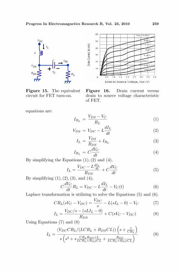
Progress In Electromagnetics Research B, Vol. 23, 2010 259
VDC
L
RDS R
L
C
VDS
IL
IRL
VC
Figure 15. The equivalentcircuit for FET turn-on.
Figure 16. Drain current versusdrain to source voltage characteristicof FET.
equations are:
IRL=
VDS − VC
RL(1)
VDS = VDC − LdIL
dt(2)
IL =VDS
RDS+ IRL
(3)
IRL= C
dVC
dt(4)
By simplifying the Equations (1), (2) and (4),
IL =VDC − LdIL
dt
RDS+ C
dVC
dt(5)
By simplifying (1), (2), (3), and (4),
CdVC
dtRL = VDC − L
dIL
dt− VC(t) (6)
Laplace transformation is utilizing to solve the Equations (5) and (6).
CRL(sVC − VDC) =VDC
s− L(sIL − 0)− VC (7)
IL =VDC/s− (sLIL − 0)
RDS+ C(sVC − VDC) (8)
Using Equations (7) and (8)
IL =(VDCCRL/(LCRL + RDSCL))
(s + 1
CRL
)
s(s2 + s CRLRDS+L
LCRL+RDSCL + RDSLCRL+RDSCL
) (9)
260 Kumar, Basu, and Koul
0 0.2 0.4 0.6 0.8 1
x 10-8
0
0.05
0.1
0.15
0.2
0.25
0.3
0.35
Inducto
r curr
ent(
Am
p)
duri
ng t
urn
-on s
tate
Time (Sec)
Figure 17. The transient responseof current is flowing in the inductorduring transistor turn-on.
5 10 15
x 10-10
-0.05
-0.04
-0.03
-0.02
-0.01
0
Cur
rent
(Am
p) d
urin
g tu
rn-o
n st
ate
Time (Sec)
Figure 18. The transient re-sponse of output current flow-ing in the load resistance duringtransistor turn-on, showing thediscontinuous dip at t = 0.
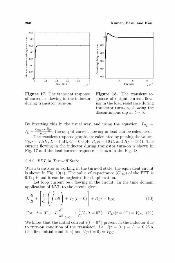
By inverting this in the usual way, and using the equation: IRL=
IL − VDC−LdILdt
RDS, the output current flowing in load can be calculated.
The transient response graphs are calculated by putting the values;VDC = 2.5V, L = 1 nH, C = 0.6 pF, RDS = 10 Ω, and RL = 50 Ω. Thecurrent flowing in the inductor during transistor turn-on is shown inFig. 17 and the load current response is shown in the Fig. 18.
2.3.2. FET in Turn-off State
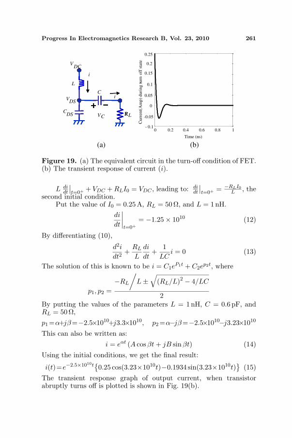
When transistor is working in the turn-off state, the equivalent circuitis shown in Fig. 19(a). The value of capacitance (CDS) of the FET is0.12 pF and it can be neglected for simplification.
Let loop current be i flowing in the circuit. In the time domainapplication of KVL to the circuit gives:
Ldi
dt+
1
C
t∫
0
idt
+ VC(t = 0)
+ RLi = VDC (10)
For t = 0+, Ldi
dt
∣∣∣∣t=0+
+1C
VC(t = 0+) + RLi(t = 0+) = VDC (11)
We know that the initial current i(t = 0+) present in the inductor dueto turn-on condition of the transistor. i.e., i(t = 0+) = I0 = 0.25A(the first initial condition) and VC(t = 0) = VDC .
Progress In Electromagnetics Research B, Vol. 23, 2010 261
VDC
L
CDS RL
C
V
i
VCR
DS
i
0 0.2 0.4 0.6 0.8 1- 0.1
-0.05
0
0.05
0.1
0.15
0.2
0.25
Cu
rren
t(A
mp
) d
uri
ng
tu
rn-
off
sta
teTime (ns)
-
(a) (b)
Figure 19. (a) The equivalent circuit in the turn-off condition of FET.(b) The transient response of current (i).
L didt
∣∣t=0+ + VDC + RLI0 = VDC , leading to: di
dt
∣∣t=0+ = −RLI0
L , thesecond initial condition.
Put the value of I0 = 0.25A, RL = 50 Ω, and L = 1 nH.di
dt
∣∣∣∣t=0+
= −1.25× 10¹⁰ (12)
By differentiating (10),
d2i
dt2+
RL
L
di
dt+
1LC
i = 0 (13)
The solution of this is known to be i = C1eP1t + C2e
p2t, where
p1, p2 =−RL
/L±
√(RL/L)2 − 4/LC
2By putting the values of the parameters L = 1 nH, C = 0.6 pF, andRL = 50 Ω,
p1 =α+jβ=−2.5×10¹⁰+j3.3×1010, p2 =α−jβ=−2.5×10¹⁰−j3.23×1010
This can also be written as:
i = eαt (A cosβt + jB sinβt) (14)
Using the initial conditions, we get the final result:
i(t)=e−2.5×10¹⁰t0.25 cos(3.23×10¹⁰t)−0.1934 sin(3.23×10¹⁰t)
(15)
The transient response graph of output current, when transistorabruptly turns off is plotted is shown in Fig. 19(b).
262 Kumar, Basu, and Koul
-0.5 0 0.5 1-0.1
-0.05
0
0.05
0.1
0.15
0.2
0.25
Outp
ut
curr
ent(
Am
p)
Time ( nSec )
9.9 10 10.1 10.2 10.3
Figure 20. The complete transient response of output current in theUWB generation circuit.
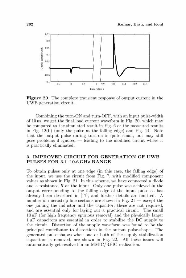
Combining the turn-ON and turn-OFF, with an input pulse-widthof 10 ns, we get the final load current waveform in Fig. 20, which maybe compared to the simulated result in Fig. 6 or the measured resultsin Fig. 12(b) (only the pulse at the falling edge) and Fig. 14. Notethat the output pulse during turn-on is quite small, but may stillpose problems if ignored — leading to the modified circuit where itis practically eliminated.
3. IMPROVED CIRCUIT FOR GENERATION OF UWBPULSES FOR 3.1–10.6GHz RANGE
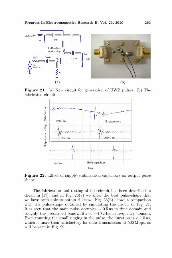
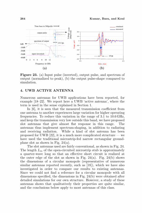
To obtain pulses only at one edge (in this case, the falling edge) ofthe input, we use the circuit from Fig. 7, with modified componentvalues as shown in Fig. 21. In this scheme, we have connected a diodeand a resistance R at the input. Only one pulse was achieved in theoutput corresponding to the falling edge of the input pulse as hasalready been described in [17], and further details are omitted. Anumber of microstrip line sections are shown in Fig. 21 — except theone joining the inductor and the capacitor, these are not required,and are essential only for laying out a practical circuit. The small10 nF (for high frequency spurious removal) and the physically larger1µF capacitors are essential in order to stabilize the DC supply tothe circuit. Distortion of the supply waveform was found to be theprincipal contributor to distortions in the output pulse-shape. Thegenerated pulse-shapes when one or both of the supply stabilizationcapacitors is removed, are shown in Fig. 22. All these issues willautomatically get resolved in an MMIC/RFIC realization.
Progress In Electromagnetics Research B, Vol. 23, 2010 263
500.6 pF
1
Diode50
BitSequence
VDC=2.5V
Vout
R
10nF
1 nH,realized
in microstrip
Vg
(a) (b)
ΩΩ
Figure 21. (a) New circuit for generation of UWB pulses. (b) Thefabricated circuit.
Outp
ut
puls
e volt
age
(200
mV
/div
)
Time
2ns / div
2ns / div
10ns / div
Both capacitors
Only 1 uF
No capacitors
2ns / div
2ns / div
10ns / div
Both capacitors
Only 1 uF
No capacitors
Figure 22. Effect of supply stabilization capacitors on output pulseshape.
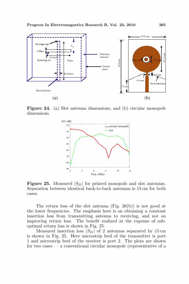
The fabrication and testing of this circuit has been described indetail in [17], and in Fig. 23(a) we show the best pulse-shape thatwe have been able to obtain till now. Fig. 23(b) shows a comparisonwith the pulse-shape obtained by simulating the circuit of Fig. 21.It is seen that the main pulse occupies ∼ 0.5 ns in time domain androughly the prescribed bandwidth of 3–10 GHz in frequency domain.Even counting the small ringing in the pulse, the duration is < 1.5 ns,which is more than satisfactory for data transmission at 500Mbps, aswill be seen in Fig. 29.
264 Kumar, Basu, and Koul
0 2 4 6 8 10 12
-40dB
-20dB
-10dB
0dB
-30dB
133.3ps
Volt
age
200m
V/d
iv
133.3ps
Frequency in GHz
Time base in 500ps/div
133.3ps
input (inverted)
output pulse
spectrum of output133.3ps133.3ps133.3ps
input (inverted)
output pulse
spectrum of output
39.5 41.0
-300
-200
-100
0
100
-400
200
time, nsec
Vout,
mV
133 ps
simulated
measured
133 ps
(a) (b)
Figure 23. (a) Input pulse (inverted), output pulse, and spectrum ofoutput (normalized to peak), (b) the output pulse-shape compared tosimulation.
4. UWB ACTIVE ANTENNA
Numerous antennas for UWB applications have been reported, forexample [18–22]. We report here a UWB ‘active antenna’, where theterm is used in the sense explained in Section 1.
In [6], it is seen that the measured transmission coefficient fromone antenna to another experiences large variation for higher operatingfrequencies. To reduce this variation in the range of 3.1 to 10.6 GHz,and keep the transmission very low outside this band, we have proposedslot antennas that give almost flat response in this range. Theantennas thus implement spectrum-shaping, in addition to radiatingand receiving radiation. While a kind of slot antenna has beenproposed for UWB [22], it is a much more complicated structure — wehave used the traditional microstrip-fed narrow rectangular ground-plane slot as shown in Fig. 24(a).
The slot antennas used are fairly conventional, as shown in Fig. 24.The length Lm of the open-circuited microstrip stub is approximatelya quarter-wave long so that an effective short circuit is realized atthe outer edge of the slot as shown in Fig. 24(a). Fig. 24(b) showsthe dimensions of a circular monopole (representative of numeroussimilar antennas reported recently, such as [18]), which we have alsoinvestigated in order to compare our results to existing antennas.Since we could not find a reference for a circular monopole with alldimensions specified, the dimensions in Fig. 24(b) were obtained afterdetailed simulations for our own structure. However, a study of theseantennas shows that qualitatively their properties are quite similar,and the conclusions below apply to most antennas of this class.
Progress In Electromagnetics Research B, Vol. 23, 2010 265
Lm
Microstrip line
Shorting strip
Radiating slot
Ground
plane
Dielectric
substrate
ng p
g
c
0.745mm
19mm
0.3mm
22.4mm
0.
3m
17 mm
5.78 mm2.99 mm
34
.73
mm
3.2 mm
0.4 mm
50.8 mm
60
.0m
m
Back-side plane
5.78 mm2.99 mm
-s e
(a) (b)
Figure 24. (a) Slot antenna dimensions, and (b) circular monopoledimensions.
-90
-80
-70
-60
-50
-40
-30
-20
2 4 6 8 10 12
Freq. (GHz)
S21 (dB)
circular monopole
slot
Figure 25. Measured |S21| for printed monopole and slot antennas.Separation between identical back-to-back antennas is 15 cm for bothcases.
The return loss of the slot antenna (Fig. 26(b)) is not good atthe lower frequencies. The emphasis here is on obtaining a constantinsertion loss from transmitting antenna to receiving, and not onimproving return loss. The benefit realized at the expense of sub-optimal return loss is shown in Fig. 25.
Measured insertion loss |S21| of 2 antennas separated by 15 cmis shown in Fig. 25. Here microstrip feed of the transmitter is port1 and microstrip feed of the receiver is port 2. The plots are shownfor two cases — a conventional circular monopole (representative of a
266 Kumar, Basu, and Koul
2 4 6 8 10 12-10
-8
-6
-4
-2
0
S11(d
B)
Frequency (GHz)
Meas .Sim.Meas .Sim.
(a) (b)
-30
-20
-10
00
30
60
90
120
150
180
210
240
270
300
330
-30
-20
-10
0
7 GHz
Norm
ali
zed
Pow
er (
dB
)
H Meas.
H Simu.
-30
-20
-10
00
30
60
90
120
150
180
210
240
270
300
330
-30
-20
-10
0 Nor
ma
lized
Pow
er (
dB
)
7 GHz
E Meas.
E Simu.
(c) (d)
Figure 26. (a) The fabricated slot antenna structure, (b) its returnloss, (c) H-plane (perpendicular to feed-line) radiation pattern at7GHz, (d) E-plane (perpendicular to slot) radiation pattern at 7 GHz.0 is perpendicular to the substrate from the feed side.
large class of UWB antennas proposed in recent times), and our newly-proposed slot antenna. It is clear that our antenna uses the 3–10 GHzband much more efficiently than the printed monopole.
The simulated E-plane and H-plane radiation pattern are similarto conventional slot antenna. Detailed study of these antennas (asregards radiation pattern and insertion loss) has been carried out andthese results will be shortly reported separately.
These fabricated slot antenna is shown in the Fig. 26(a), its returnloss (measured with microstrip TRL calibration and simulated) inFig. 26(b), its H-plane radiation pattern (measured and simulated)at a mid-band frequency of 7GHz in Fig. 26(c), and E-plane radiationpattern (measured and simulated) in Fig. 26(d). The agreementbetween measured and simulated data is fairly good — the onlydiscrepancy which we cannot explain yet is the 0.5 GHz shift in thefrequency of best return loss. The most probable explanation is changein dielectric constant from the manufacturer-specified 2.2 at 10MHz
Progress In Electromagnetics Research B, Vol. 23, 2010 267
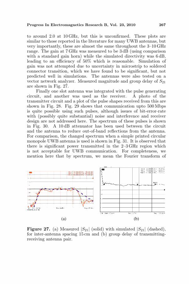
to around 2.0 at 10 GHz, but this is unconfirmed. These plots aresimilar to those reported in the literature for many UWB antennas, butvery importantly, these are almost the same throughout the 3–10 GHzrange. The gain at 7 GHz was measured to be 3 dB (using comparisonwith a standard gain horn) while the simulated directivity was 6 dB,leading to an efficiency of 50% which is reasonable. Simulation ofgain was not attempted due to uncertainty in microstrip to solderedconnector transition, which we have found to be significant, but notpredicted well in simulations. The antennas were also tested on avector network analyzer. Measured magnitude and group delay of S21
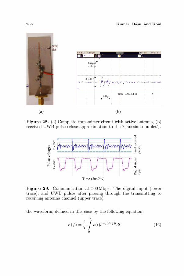
are shown in Fig. 27.Finally one slot antenna was integrated with the pulse generating
circuit, and another was used as the receiver. A photo of thetransmitter circuit and a plot of the pulse shapes received from this areshown in Fig. 28. Fig. 29 shows that communication upto 500 Mbpsis quite possible using such pulses, although issues of bit-error-ratewith (possibly quite substantial) noise and interference and receiverdesign are not addressed here. The spectrum of these pulses is shownin Fig. 30. A 10 dB attenuator has been used between the circuitand the antenna to reduce out-of-band reflections from the antenna.For comparison, the changed spectrum when a simple printed circularmonopole UWB antenna is used is shown in Fig. 31. It is observed thatthere is significant power transmitted in the 2–3GHz region whichis not acceptable for UWB communication. For completeness, wemention here that by spectrum, we mean the Fourier transform of
(a) (b)
Figure 27. (a) Measured |S21| (solid) with simulated |S21| (dashed),for inter-antenna spacing 15 cm and (b) group delay of transmitting-receiving antenna pair.
268 Kumar, Basu, and Koul
Time (0.5ns / div)689ps
2.19mV
Output
voltage
(a) (b)
Figure 28. (a) Complete transmitter circuit with active antenna, (b)received UWB pulse (close approximation to the ‘Gaussian doublet’).
Time (2ns/div)
Pu
lse
vo
ltag
es
Dig
ital
sig
nal
inp
ut
Fin
al r
ecei
ved
pu
lses
1V
/div
1m
V/d
iv
Figure 29. Communication at 500 Mbps: The digital input (lowertrace), and UWB pulses after passing through the transmitting toreceiving antenna channel (upper trace).
the waveform, defined in this case by the following equation:
V (f) =1T
T∫
0
v(t)e−j(2πf)tdt (16)
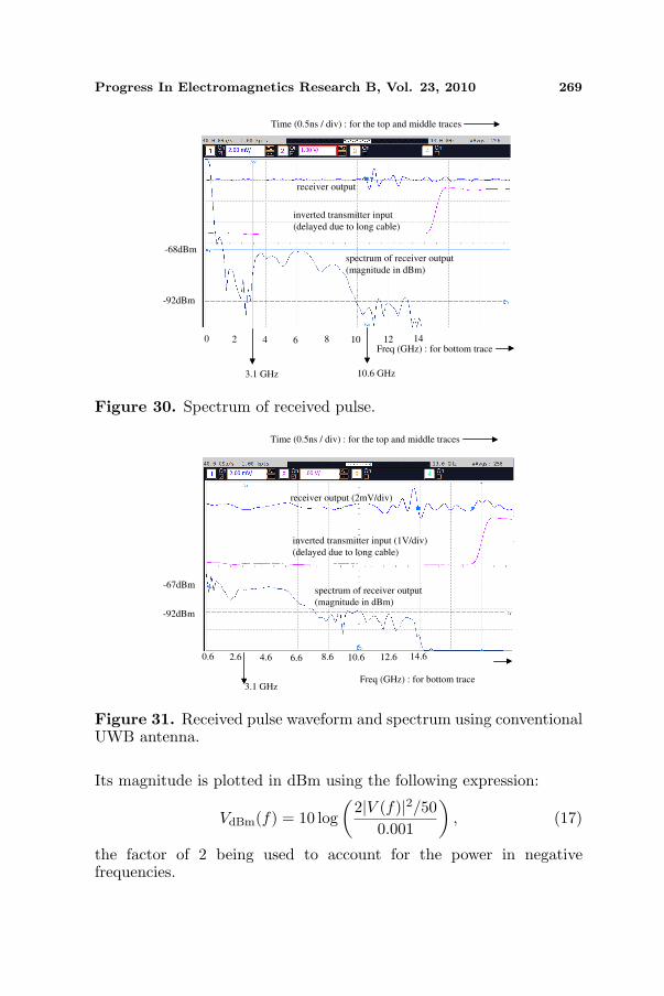
Progress In Electromagnetics Research B, Vol. 23, 2010 269
-68dBm
-92dBm
Time (0.5ns / div) : for the top and middle traces
Freq (GHz) : for bottom trace0 2 4 6 8 10 12 14
3.1 GHz 10.6 GHz
receiver output
inverted transmitter input
(delayed due to long cable)
spectrum of receiver output
(magnitude in dBm)
receiver output
inverted transmitter input
(delayed due to long cable)
spectrum of receiver output
(magnitude in dBm)
Figure 30. Spectrum of received pulse.
-67dBm
-92dBm
Time (0.5ns / div) : for the top and middle traces
Freq (GHz) : for bottom trace
0.6 2.6 4.6 6.6 8.6 10.6 12.6 14.6
3.1 GHz
receiver output (2mV/div)
spectrum of receiver output
(magnitude in dBm)
inverted transmitter input (1V/div)
(delayed due to long cable)
receiver output (2mV/div)
spectrum of receiver output
(magnitude in dBm)
inverted transmitter input (1V/div)
(delayed due to long cable)
Figure 31. Received pulse waveform and spectrum using conventionalUWB antenna.
Its magnitude is plotted in dBm using the following expression:
VdBm(f) = 10 log(
2|V (f)|2/500.001
), (17)
the factor of 2 being used to account for the power in negativefrequencies.
270 Kumar, Basu, and Koul
For an oscilloscope sampling rate of N samples/sec, and a data setof P points, T obviously comes out to (P/N) sec. N and P are displayedwith the plots above.
5. CONCLUSION
A novel UWB pulse generating circuit and an active UWB antennahave been developed. This circuit is the simplest known for generatingUWB pulses, is low cost and is compatible with MMIC (and probablyRF-CMOS with simple modifications), which is important for practicalUWB systems. In future UWB communication systems which includeantenna arrays, multiple transmitters and appropriate receiver will bedeveloped.
ACKNOWLEDGMENT
The authors wish to acknowledge the assistance of Agilent Technologiesfor providing the high-speed oscilloscope and for a donation of ADSsoftware.
REFERENCES
1. Ghavami, M., L. B. Michael, and R. Kohno, Ultra WidebandSignals and Systems in Communication Engineering, John Wiley& Sons, Ltd, England, 2004.
2. Federal Communications Commission, “First report and order,”Feb. 14, 2002.
3. Ammann, M. J. and Z. N. Chen, “Wideband monopole antennafor multi-band wireless system,” IEEE Antenna Propag. Mag.,Vol. 45, No. 2, 146–150, 2003.
4. Kharakhili, F. G., M. Fardis, G. Dadashzadeh, A. K. A. Ahmadi,and N. Hojjat, “Circular slot with a novel circular microstripopen ended microstrip feed for UWB applications,” Progress InElectromagnetics Research, Vol. 68, 161–167, 2007.
5. Chen, H.-D. and H.-T. Chen, “A CPW-fed dual-frequencymonopole antenna,” IEEE Trans. Antenna Propagation, Vol. 52,978–982, Apr. 2004.
6. Antonino, D. E., F. M. Cabedo, B. Ferrando, and A. J. Villa,“Active UWB antenna with tunable band-notch behaviour,”Electronics Letters, Vol. 43, No. 18, Aug. 31, 2007.
Progress In Electromagnetics Research B, Vol. 23, 2010 271
7. Lin, C.-C. and H.-R. Chuang, “A 3–12 GHz UWB planartriangular monopole antenna with ridged ground-plane,” ProgressIn Electromagnetics Research, Vol. 83, 307–321, 2008.
8. Chen, Z. N., Antenna for Portable Devices, John Wiley & Sons,Ltd, England, 2007.
9. Kumar, M., A. Basu, S. K. Koul, and B. Bhat, “Active suspendedmicrostrip patch antenna,” PIERS Proceedings, 180, Osaka,Japan, Jul. 18–22, 2001.
10. Ma, T.-G., C.-J. Wu, and C.-F. Chou, “An impulse-radio-basedultrawideband RF front-end module with a new multilayeredmicrowave sampler,” Progress In Electromagnetics Research,Vol. 86, 1–18, 2008.
11. Jeong, S. L. and C. Nguyen, “Novel low-cost ultra-wideband,ultra-short-pulse transmitter with MESFET impulse-shapingcircuitry for reduced distortion and improved pulse repetitionrate,” IEEE Microwave and Wireless Components Letters, Vol. 11,No. 5, 208–210, May 2001.
12. Saha, P. K., N. Sasaki, and T. Kikkawa, “A CMOSUWB transmitter for intra/inter-chip wireless communication,”International Symposium on Spread Spectrum Techniques andApplications 2004, 962–966, Sep. 2004.
13. Ryckaert, J., et al., “Ultra-wide-band transmitter for low powerwireless body area networks: Design and evaluation,” IEEETransactions on Circuits and Systems, Vol. 52, 2515–2525,Dec. 2005.
14. Kim, H. and Y. Joo, “Fifth-derivative Gaussian pulse generatorfor UWB system,” IEEE Radio Frequency Integrated CircuitsSymposium, 671–674, Jun. 2005.
15. Norimatsu, T., et al., “A novel UWB impulse-radio transmitterwith all-digitally-controlled pulse generator,” European Solid-stateCircuits Conference 2005, 267–270, 2005.
16. Kumar, M., A. Basu, and S. K. Koul, “A novel scheme forgenerating and transmitting UWB signals,” Proceedings of 2009IEEE International Conference on Antennas, Propagation andSystems (INAS 2009), Johor Bahru, Malaysia, Dec. 3–5, 2009.
17. Kumar, M., A. Basu, and S. K. Koul, “Electromagnetic shortpulse generation techniques,” The 2010 International Symposiumon Electromagnetic Theory (EMTS 2010), Berlin, Germany,Aug. 16–19, 2010.
18. Liang, J., L. Guo, C. C. Chiau, X. Chen, and C. G. Parini, “Studyof CPW-fed circular disc monopole antenna for ultra wideband
272 Kumar, Basu, and Koul
applications,” IEE Proceedings on Microwaves, Antennas andPropagation, IET Journals, 520–526, 2005.
19. Chen, D. and C. H. Cheng, “A novel compact ultra-wideband(UWB) wide slot antenna with via holes,” Progress InElectromagnetics Research, Vol. 94, 343–349, 2009.
20. Sadat, S., M. Houshmand, and M. Roshandel, “Design of amicrostrip square-ring slot antenna filled by an H-shape slotfor UWB applications,” Progress In Electromagnetics Research,Vol. 70, 191–198, 2007.
21. Zaker, R., C. Ghobadi, and J. Nourinia, “A modified microstrip-FED two-step tapered monopole antenna for UWB and WLANapplications,” Progress In Electromagnetics Research, Vol. 77,137–148, 2007.
22. Siahcheshm, A., S. Sadat, C. H. Ghobadi, and J. Nourinia,“Design of a microstrip slot antenna filled by an isosceles trianglefor UWB applications,” Journal of Electromagnetic Waves andApplications, Vol. 22, No. 1, 111–118, 2008.