circuit board having shielding planes with varied void opening patterns for controlling the...
Post on 20-Dec-2015
213 views
TRANSCRIPT
Circuit Board Having Shielding Planes with Varied Void Opening Patterns for Controlling the Impedance and the
Transmission Time of Differential Transmission Lines
Chi-Kuang HwangDept. of Electrical EngineeringChung-Hua University
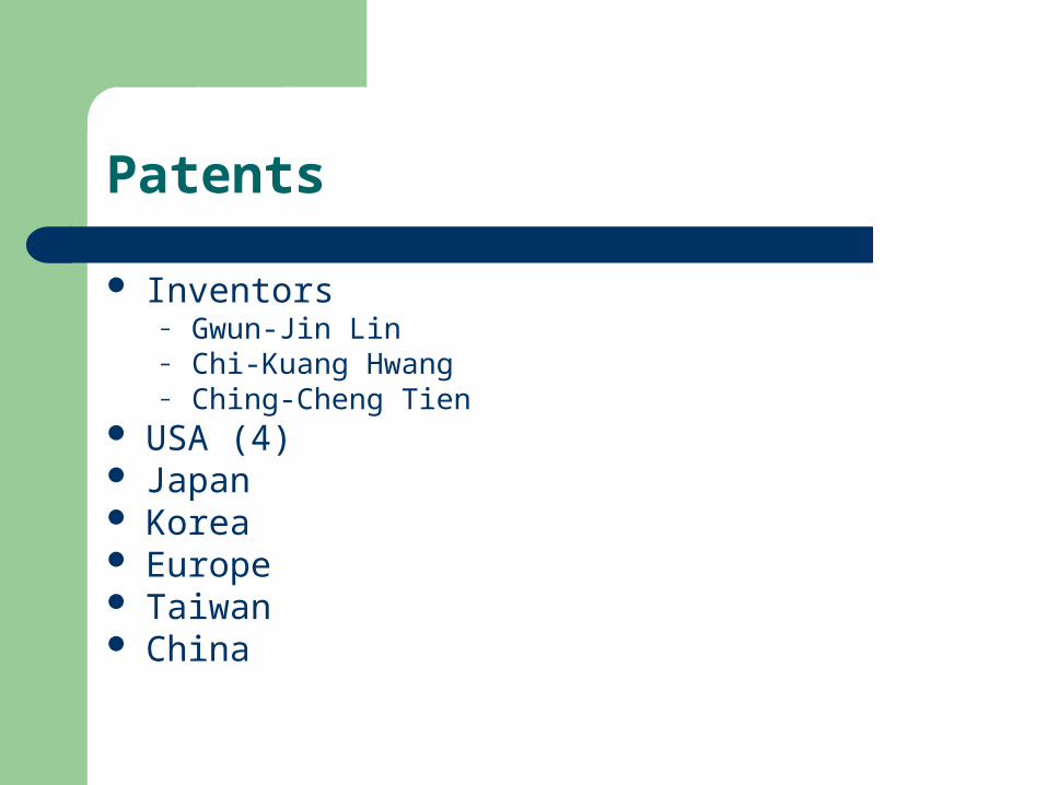
Patents
Inventors– Gwun-Jin Lin– Chi-Kuang Hwang– Ching-Cheng Tien
USA (4) Japan Korea Europe Taiwan China
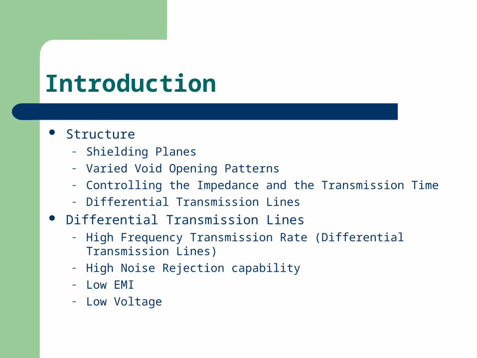
Introduction
Structure – Shielding Planes– Varied Void Opening Patterns– Controlling the Impedance and the Transmission Time– Differential Transmission Lines
Differential Transmission Lines– High Frequency Transmission Rate (Differential Transmission
Lines)– High Noise Rejection capability– Low EMI– Low Voltage
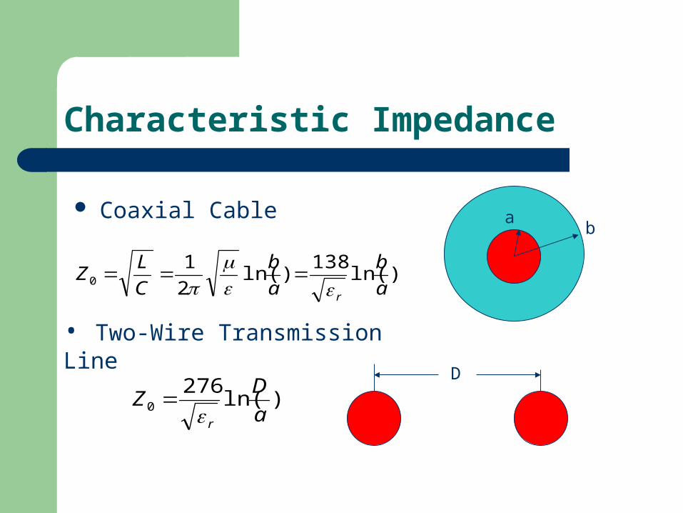
Characteristic Impedance
Coaxial Cable
)ln(276
0 a
DZ
r
)ln(138
)ln(2
10 a
b
a
b
C
LZ
r
• Two-Wire Transmission Line
D
ab
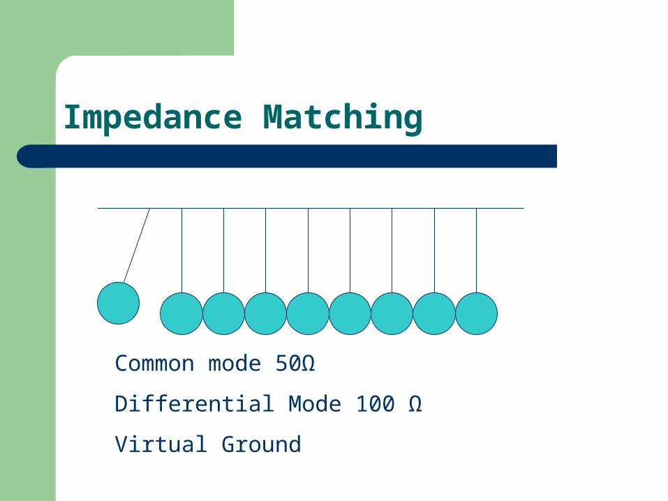
Impedance Matching
Common mode 50Ω
Differential Mode 100 Ω
Virtual Ground
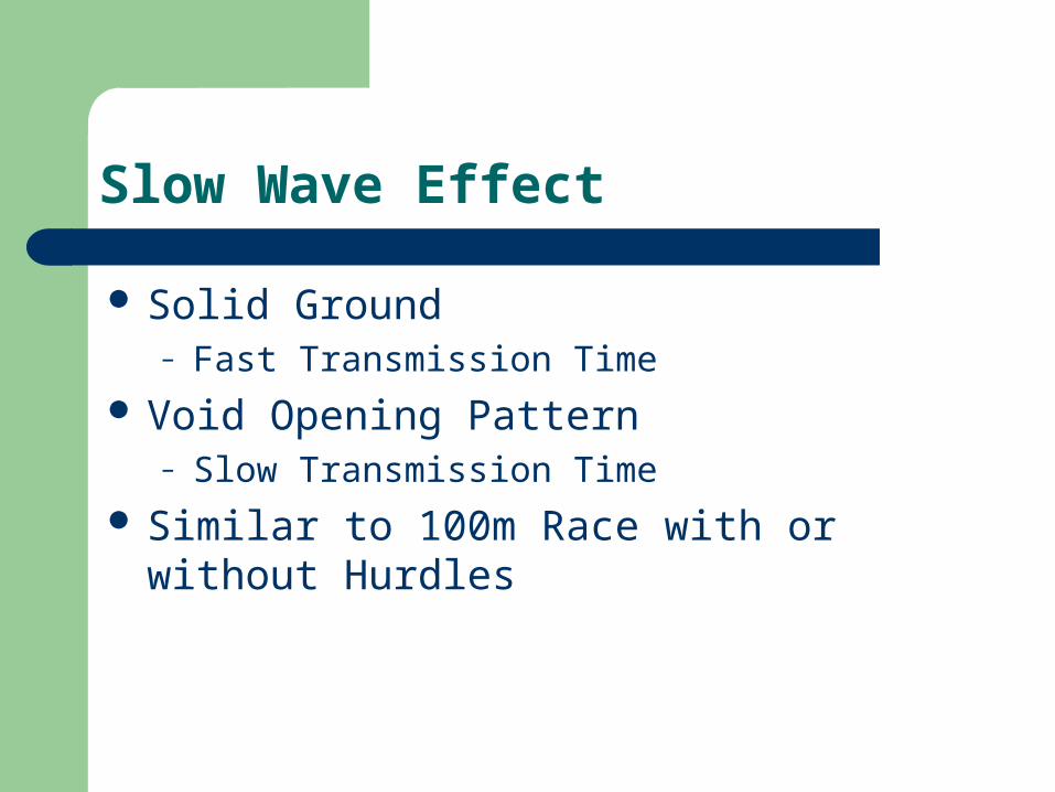
Slow Wave Effect
Solid Ground – Fast Transmission Time
Void Opening Pattern– Slow Transmission Time
Similar to 100m Race with or without Hurdles
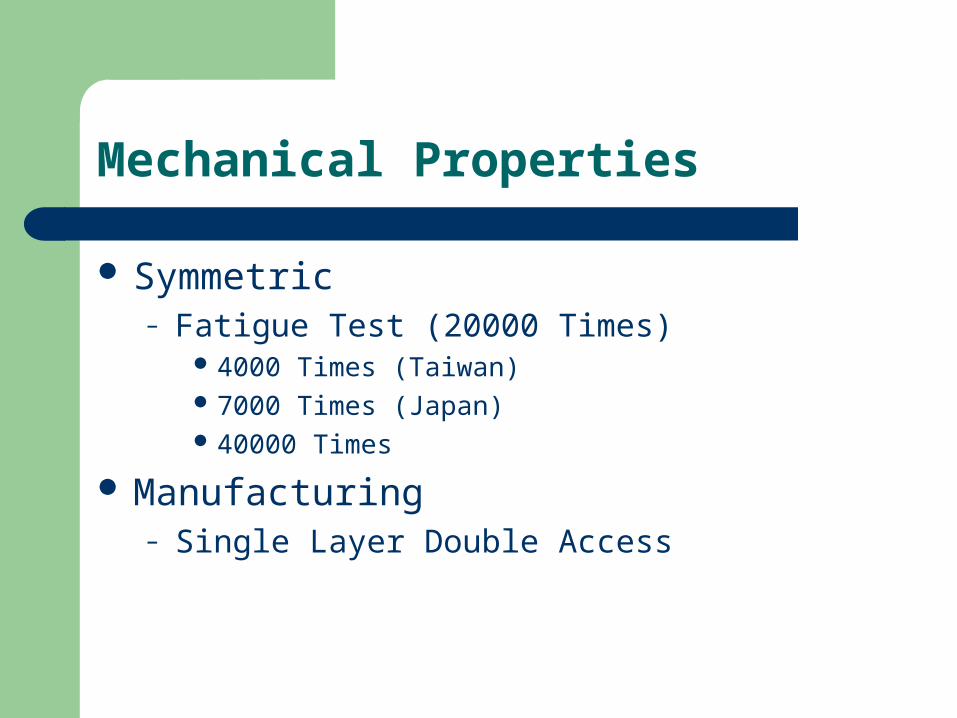
Mechanical Properties
Symmetric– Fatigue Test (20000 Times)
4000 Times (Taiwan) 7000 Times (Japan) 40000 Times
Manufacturing– Single Layer Double Access
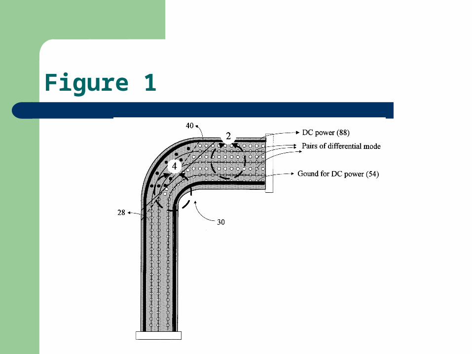
Figure 1
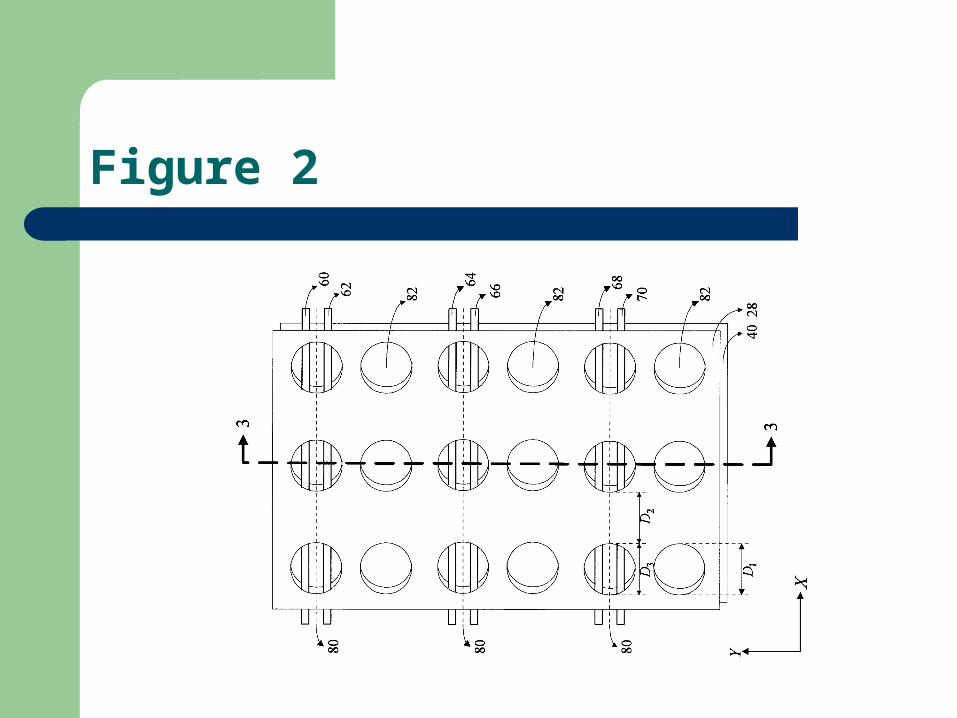
Figure 2
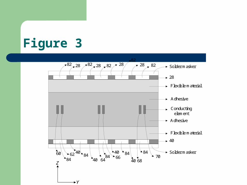
Figure 3
Flexible material
Adhesive
Solder masker
Adhesive
Z
82
84
82 82
60 6264
6668
708484
4040
2828 Solder masker
Flexible material
28
2882
82 28
40
40 844084
Conducting element
Y
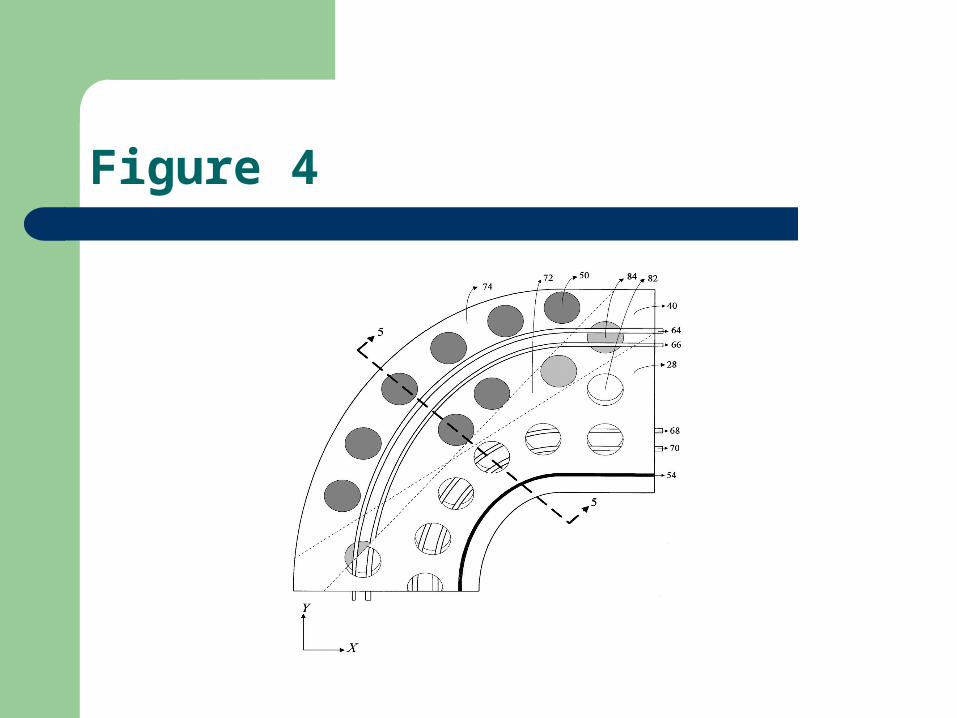
Figure 4
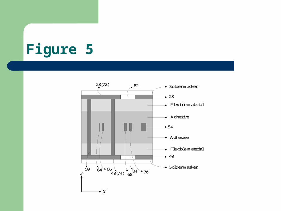
Figure 5
Flexible material
Adhesive
Solder masker
Adhesive
Z
82
64 6668
708440(74)
28(72) Solder masker
Flexible material
28
40
54
X
50
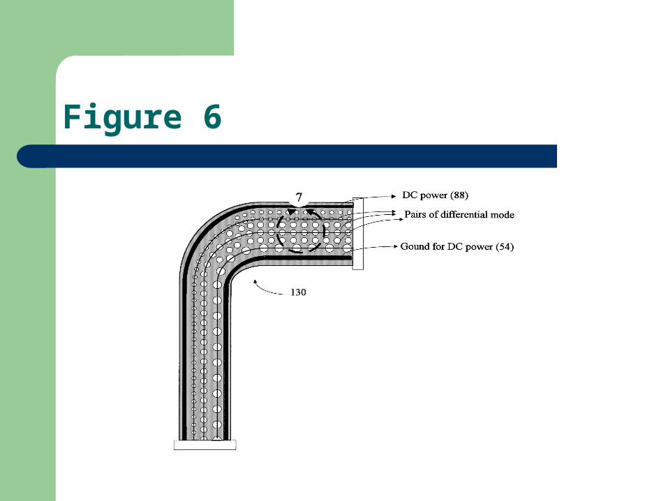
Figure 6
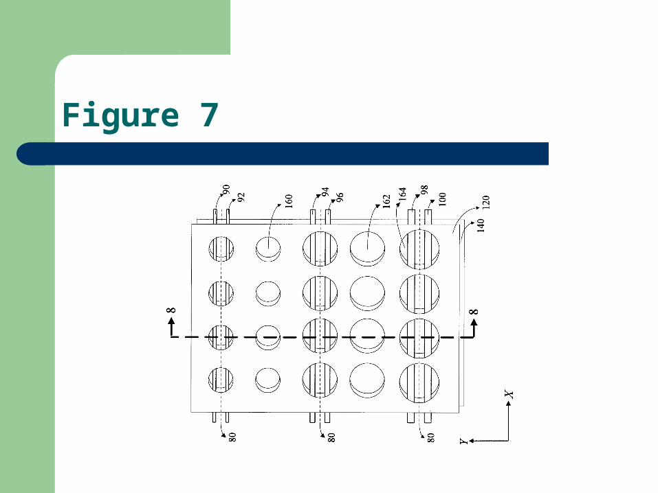
Figure 7
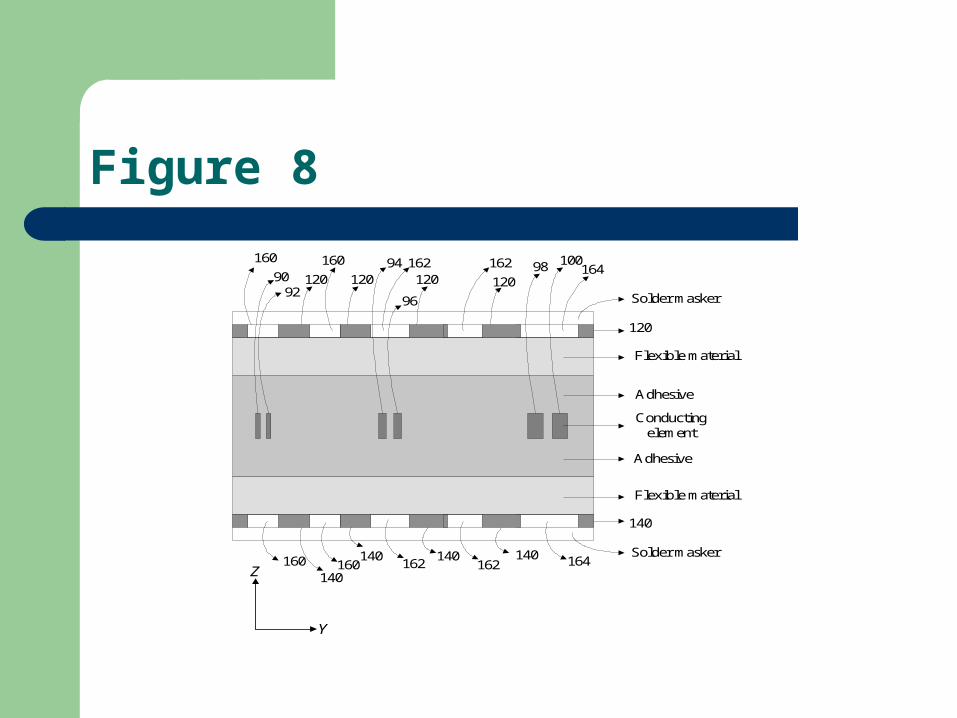
Figure 8
Z
96
94
9290
162 98 100
120164
160
164140 140 140160 162
120 120
Y
160
120162
Flexible material
Adhesive
Solder masker
Adhesive
Solder masker
Flexible material
120
140
Conducting element
162160140
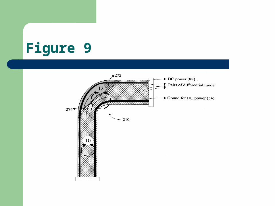
Figure 9
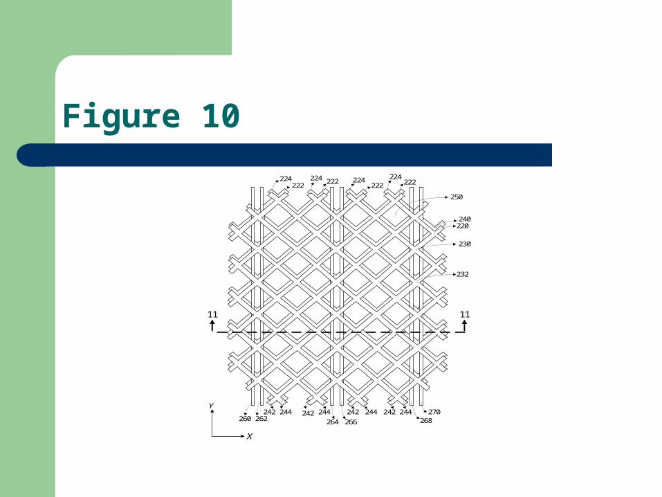
Figure 10
260
1111
X
Y
262242 244 242 244242 244
264 266
242 244268
270
232
230
220240
250
224 224 224 224222
222222 222
Figure 11
X
Z270260
240262
264
240
266
268
220220220
250
250250
250250
220250 250 250 250 250
Flexible material
Adhesive
Solder masker
Adhesive
Solder masker
Flexible material
Conducting element
220
240
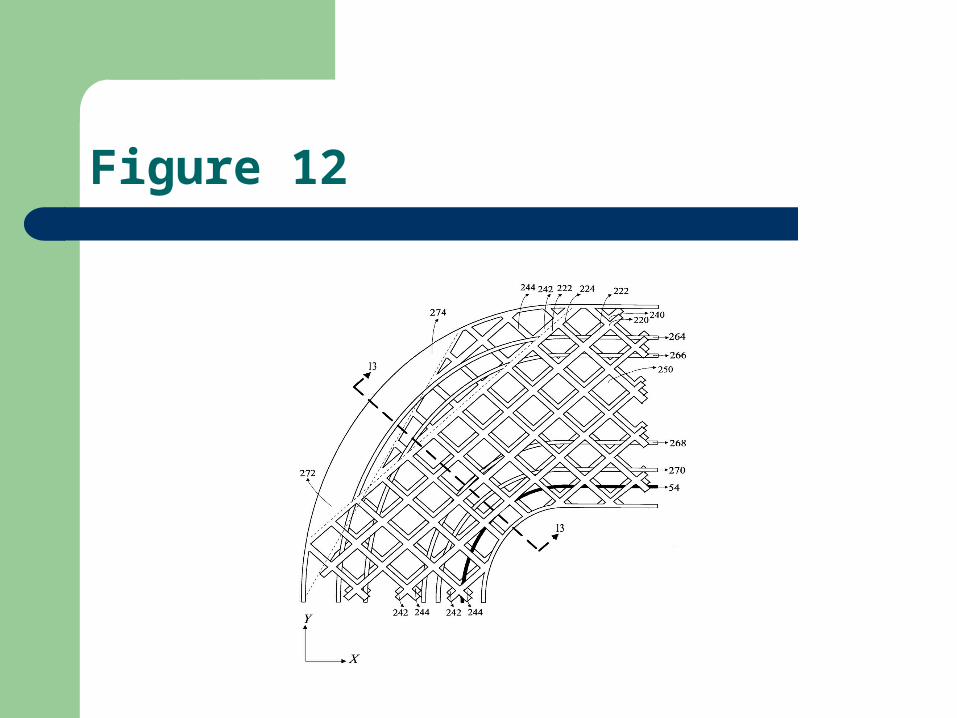
Figure 12
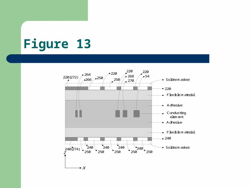
Figure 13
X
Z
220(272)220264
266
220268270
240(274) 240
240
250 250
220
54
Flexible material
Adhesive
Solder masker
Adhesive
Solder masker
Flexible material
Conducting element
220
250240 240
250 250 250 250240
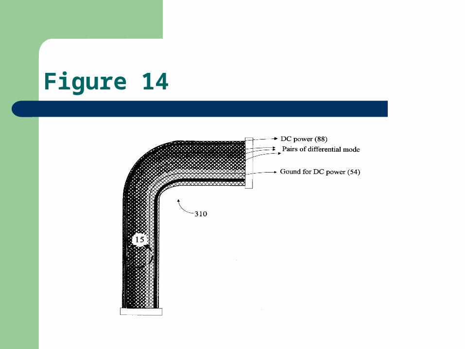
Figure 14
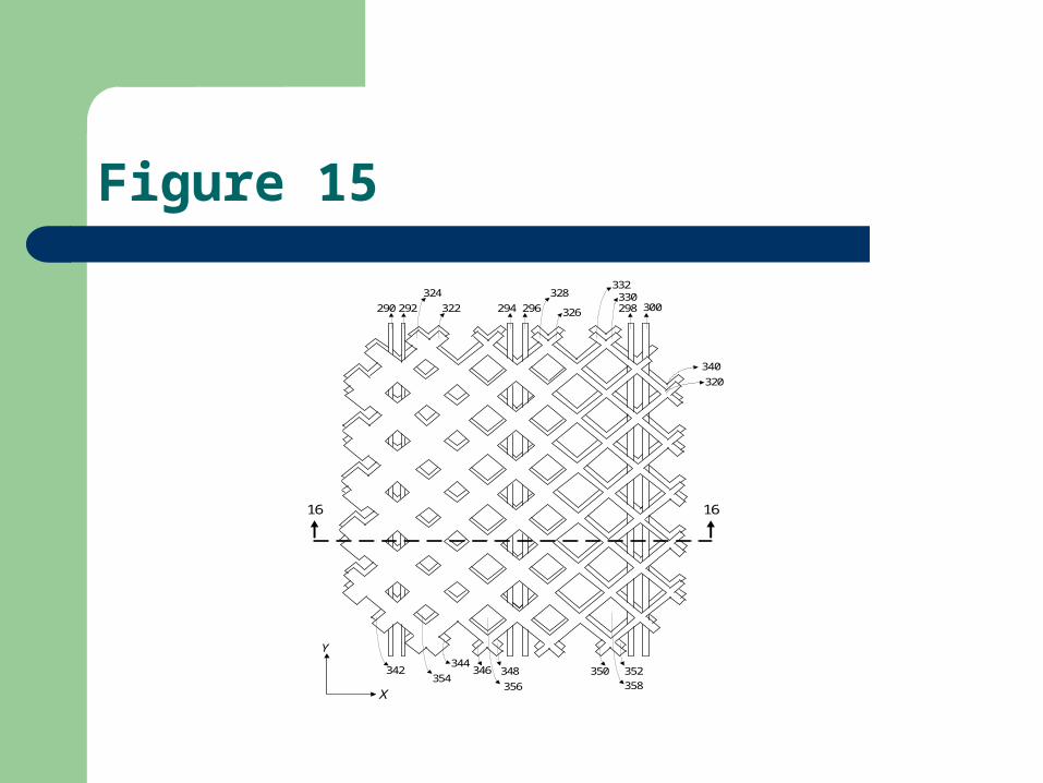
Figure 15
X
Y
290 292
324
322 294 296
328
326
332330298 300
340
320
352350348346344
342354
356 358
1616

Figure 16
Flexible material
Adhesive
Solder masker
Adhesive
Z 354
354
290 292
320 Solder masker
Flexible material
320
340
340
Conducting element
320320 320354
356 358
358
354
340
294296
356340
340
358
298 300358
X
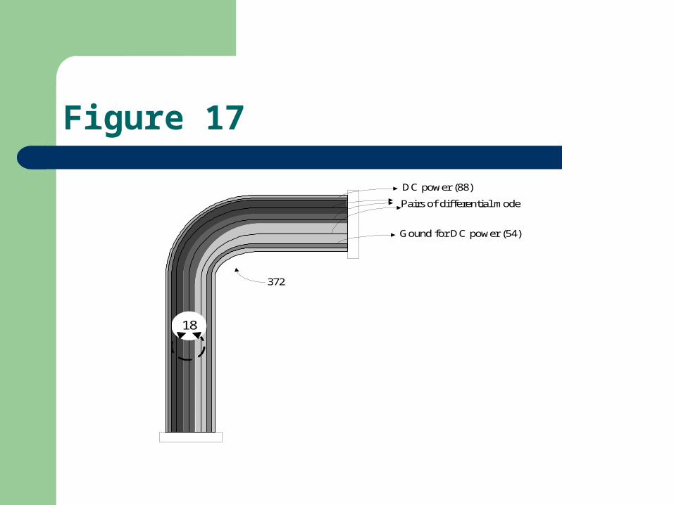
Figure 17
18
372
Pairs of differential mode
Gound for DC power (54)
DC power (88)
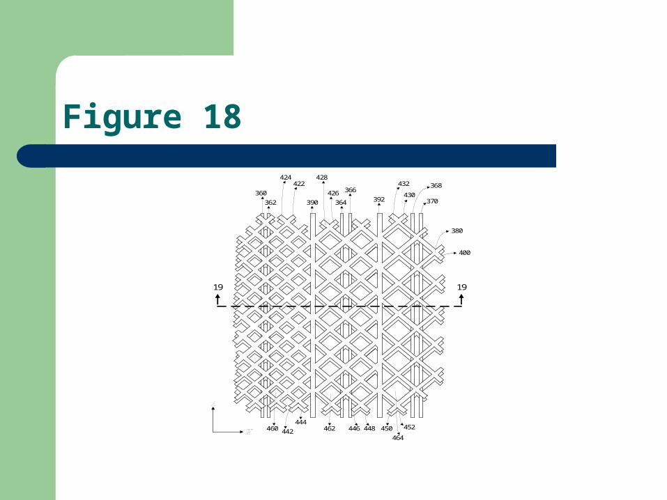
Figure 18
452450448446444
442464
462460
400
380
432428
366
364390
424422
362
360 426392
430
368
370
19 19
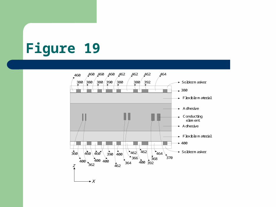
Figure 19
Flexible material
Adhesive
Solder masker
Adhesive
Z400
460
360
362
380 Solder masker
Flexible material
380
400
400
Conducting element
400
390
364
366400 462
392400368 370
464
460
380
460 460
380 390 380 380 392
462 462 462 464
460 460
462
462
X
Applications
Computers and Communications– Notebook– Cellular Phone– PDA
Display– LCD
Testing Cables
Connectors Testing Cables Standard Cables Non-Adhesive Flexible Cables
– Chip On Film (COF)
Single Layer Double Access