chapter4-self commutating conversin
DESCRIPTION
Self commutating conversion..TRANSCRIPT

1
Self-Commutating Conversion
Flexible Power Transmission-The HVDC Option

2
Introduction
• Line Commutated Convertors Shortcomings– Large reactive power requirement (both during
rectification and inversion),– Injection of low-order harmonic currents– Risk of inverter commutation failures– Dependence on reasonably strong AC systems to
provide the commutating voltages.– These problems can be eliminated in self-
commutated conversion by the use of more advanced switching devices with turn-on and turn-off capability (IGBT)
3
Voltage Source Converters (VSC)• Power transmission system requires precise control of active
and reactive power flow to maintain the system voltage stability. This is achieved through an electronic converter and its ability of converting electrical energy from AC to DC or vice versa.
• Voltage Source Converters operating with the specified vector control strategy can perform independent control of active/reactive power at both ends. This ability of VSC makes it suitable for connection to weak AC networks, i.e. without local voltage sources. For power reversal, the DC voltage polarity remains the same for VSC based transmission system and the power transfer depends only on the direction of the DC current.

4
LCC - VSC ComparisonLCC HVDC• Mature Technology• Requires strong ac system• Lower losses 0.8% per converter• Requires 60% reactive power• AC-DC system interactions• Harmonics• Commutations failure• Special Transformers• Multi terminal operation possible
but hard• Controlled DC Current to zero
(Idref=0)• Dc voltage + to - as alpha changes• rectifier to inverter
VSC HVDC
• Rapid growth• Helps ac system• Control real and reactive power• independently• Losses reducing 1.1- 1.2% per
converter• No Commutation failure• Less Special Transformers• Flexible Dispatch• Harmonics with MMC no issue• DC Grid (multi-terminal) possible• DC voltage is a constant polarity• DC Line faults are problematic

5
Line-Commutated Converters (LCC)
• Depends on the line voltage of the connected AC System for commutation
• Use uncontrolled or semi-controlled switching devices (diodes & thyristors)
• Fixed DC current direction• Large inductance enables it to be almost constant• Direction of power flow controlled through reversal of the
polarity of DC voltage• On the AC side, behaves approximately as a current source,
injecting both grid-frequency and harmonic currents• 6-pulse and 12-pulse configuration

6
Voltage Source Convertor• self-commutated converters• Use IGBT with turn-on and turn-off control• Fixed polarity of DC voltage • Constant, smoothed by a large capacitance• Power reversal by reversing current direction• Easier to connect into a Multi-terminal HVDC system or “DC Grid”• More compact than LCC as mainly much less harmonic filtering is
required• VSC HVDC systems normally use the six-pulse connection • Less harmonic distortion as compared to LCC• Simplified construction of the converter transformer• Basically a VSC generates ac voltage from a dc voltage. It is, for
historical reasons, often referred to as an inverter, even though it has the capability to transfer power in either direction

7
Two-level VSC Operating Principles
• Two-level VSC Operating Principles• The converter valves are assumed lossless• DC capacitors ripple negligible• The converter transformer lossless

8
Two-level VSC Operating Principles
• Two-level single phase VSC• AC terminals are switched in a bipolar
way between two discrete voltage levels (+Vd & −Vd)
• Conducting period is 180o, square wave switching scheme
• Since the conduction in switch is unidirectional, anti parallel diode (free-wheeling) is connected across to ensure the bridge voltage has one polarity & current can flow in both directions
• Capacitor mid point is reference for AC output voltage

9
Two-level VSC Operating Principles
• S1 is ON,
• +ve current will flow through S1
• S2 is ON,
• -ve current will flow through S2
• Both switches OFF, AC present• Diode forms uncontrolled rectifire• Charge Capacitors
• -ve current will flow through D1
• +ve current will flow through D2
2VdcVac
2VdcVac

10
Two-level VSC Operating Principles
• Only one switch at a time is ON• Simultaneous ON will result short
circuit • Blanking period-diode conducts
• S1 ON
• S1OFF- Inductance maintains present current, D2 conduct, voltage reverse polarity
• S2 ON, current reversal
• S2 OFF, D1 conducts
• Operates in four quadrants

11
Single-phase full wave bridge
• DC capacitor -stiff voltage• Two AC connection points• 1-4 valves – sequence of turn-off & on• 1-2 ON, a+ & b- , vab=+Vd• 3-4 ON, a- & b+, vab= -Vd• Vab is independent of ac current flow• The ac current is the result of interaction of the
converter generated ac voltage with the ac system voltage and impedance– T1-t2- 1-2 ON, vab+, iab-, dc to ac, INV– T2-t3, 1-2 ON, vab+, iab+, ac t- dc, RECT– T3-t4, 3-4 ON, vab-, iab+, ,dc to ac, INV– T4-t5, 3-4 ON, vab-, iab-, ac to dc, RECT
• Id-cuurent flow in dc bus– + ac to dc & -dc to ac
• Power flow from ac to dc with lagging power factor

12
Single-phase full wave bridge

Single-phase full wave bridge• DC capacitor -stiff voltage• Two AC connection points• 1-2 ON, a+ & b- , vab=+Vd• 3-4 ON, a- & b+, vab= -Vd• Vab is independent of ac current
flow• The ac current is the result of
interaction of the converter generated ac voltage with the ac system voltage and impedance– T1-t2- 1-2 ON, vab+, iab-, dc to ac,
INV– T2-t3, 1-2 ON, vab+, iab+, ac t- dc,
RECT– T3-t4, 3-4 ON, vab-, iab+, ,dc to ac,
INV– T4-t5, 3-4 ON, vab-, iab-, ac to dc,
RECT
• Id-cuurent flow in dc bus– + ac to dc & -dc to ac
• Power flow from ac to dc with lagging power factor
13
ac volt.
ac current
dc current
Vab
iab
id

14
Power Transfer Control
• Passive load on AC Side– Power flow is unidirectional from DC input side to
passive AC load
• Active load on AC side– Power flow is bi-directional in either direction– Phase angle of AC o/p voltage +ve or –ve w.r.t AC
system voltage

15
Inverter Operation-P & Q
• Active and Reactive Power exchange depends on phase angle and magnitude of ends voltages
• For reactive power compensation no DC source required

16
Inverter Operation-different conditions
• If δ>0 & V2>V1, P is transferred from VSC to AC system, else reverse
• If δ=0, V1=V2, No P & Q is exchanged
• V2>V1, I/90o capacitive action (generate Q)
• V2<V1, I/-90o-Inductive action (absorb Q)

17
VSC Components
• Voltage source on DC side• DC Capacitor• Switches• Reactor• Transformer• Filters• Control• Monitoring• Protection

18
DC Capacitor• Strongly capacitive, and thus voltage stiff• Establish voltage across switches• Required - Voltages are well defined and
independent of convertor operation• Practically– produce harmonics currents on DC side– Results in harmin voltages and DC voltage ripple
• Size of C inversely related to switching frequencies• Capacitor current direction changes with valve
switching

19
Coupling Reactance
• Between AC system & Converter terminal• Includes transformer Reactance & added reactor• Reduces fault current• Stabilizes AC current• Reduce harmonic current content• Control P & Q from the VSC• AC filter included to reduce the high-frequency
voltage stresses

20
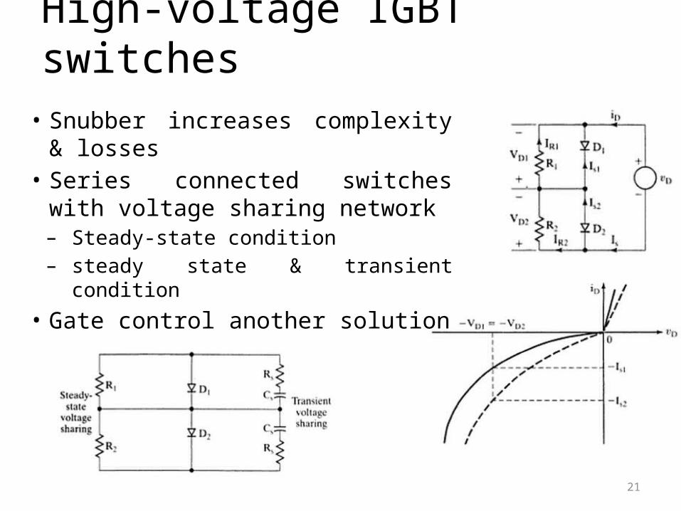
High-voltage IGBT switches
• Self Commutating • Series connected for high-voltage applications• Single IGBT valve comprises of– Switching device– Snubber to protect from V & I transients. Also equal
voltage sharing– Gate drive to turn ON & OFF the switch– Protection (over & under voltage, over current)
21
High-voltage IGBT switches
• Snubber increases complexity & losses
• Series connected switches with voltage sharing network– Steady-state condition– steady state & transient condition
• Gate control another solution

22
High-voltage IGBT switches
• Turn-on delay time variation with temperature• Turn of delay– Temperature, commutated current, fall time
• di/dt control through inductor– Reduce turn on losses,
• Series connected IGBTs for specific rating must be increased for redundancy in case of failure of one device
• Failed device avoid open-ckt and establish short circuit to conduct current

23
High-voltage IGBT switches• Unlike LCC switches, VCC switches withstand more high
voltages for a substantial part of its operation time and, therefore, the probability of avalanche current is increased.
• The valves have to withstand peak current due to ripple and transient over-current levels and require additional protection margin;
• Valves also need to be capable of turning off the current following a short circuit close to the valve itself.
• Gate unit must maintain safe device operation during short-circuit conditions.
• The IGBT is better behaved in this respect

24
The anti-parallel diodes• The anti-parallel diodes in the VSC bridge constitute an uncontrolled
bridge rectifier • Diodes have to be designed to withstand the fault-created stresses.• A DC short-circuit fault creates a current path through the diodes and
the fault current is limited only by the AC system and converter impedances. This fault current needs to be cleared by a circuit breaker on the AC side, which will require a few cycles to operate.
• The diode will also experience inrush current and an overvoltage on the DC bus.
• Overvoltage must be limited by external components• The DC capacitor can be charged independently prior to converter
energisation. In this case a DC blocking voltage will appear after the initial current surge.

25
Three-phase full-wave bridge VSC

26
The Three-phase VSC• Six-pulse VSC Consists of a three-phase bridge connecting the
AC source to a predominantly capacitive DC system• The bridge valve unit is an asymmetric turn-off device (GTO)
with a reverse-connected diode in parallel. • The turn-off device carries out the instantaneous inverter
function• The diode is needed to provide a path for the transfer of energy
from the AC to the DC side (i.e. rectifier operation) to charge the capacitor.
• During each cycle there will be periods of rectification and inversion determined by the phase angle
• The average current will determine the net power flow direction (i.e. rectification or inversion)

27
The Three-phase VSC• If the converter operates as a rectifier with unity power factor,
only the diodes conduct the current• During inverter operation with unity power factor only the turn-
off devices conduct.• By appropriate control of the turn-on and turn-off switching, a
three-phase AC waveform is produced at the AC output.• For fast transients the DC capacitor can be regarded as a perfect
voltage source.• Thus in the short time sequence in which the switching devices
are controlled to interconnect the DC and AC terminals, the DC voltage remains practically constant and the VSC produces a quasi-square-wave AC voltage.
28
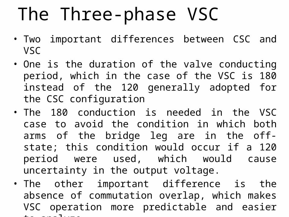
The Three-phase VSC• Two important differences between CSC and VSC• One is the duration of the valve conducting period, which in the
case of the VSC is 180 instead of the 120 generally adopted for the CSC configuration
• The 180 conduction is needed in the VSC case to avoid the condition in which both arms of the bridge leg are in the off-state; this condition would occur if a 120 period were used, which would cause uncertainty in the output voltage.
• The other important difference is the absence of commutation overlap, which makes VSC operation more predictable and easier to analyze.

29
The Three-phase VSC• The switches of an leg cannot be switched ON or OFF simultaneously• Order 1 to 6 represents the sequence of valve operation in time• Three phase-legs, which operate in concert, 120 degrees apart• Square wave mode, 180o ON, 180o OFF
• vaN, vbN, vcN are phase voltages w.r.t. Capacitor mid point, N
• vab, vbc,vca are line voltages
• vnN is the voltage of T/F neutral w.r.t. capacitor mid point , N
• equals the sum of the instantaneous potentials of the three phases vaN, vbN, vcN and is a square AC waveform varying at three times the fundamental frequency, with a magnitude equal to one-sixth of the DC voltage.
• van, vbn, vcn The phase voltage across the star-connected transformer secondary.
• vp-p=0 for 60o, two valves on the same side of the dc bus are closed on their dc bus

30
Three-phase full-wave bridge VSC

31
Switch states

32
AC voltage waveforms-gate sequence

33
AC voltage waveforms

34
AC waveforms

AC waveforms
35

36
DC current waveforms

37
AC voltage waveforms• The current flow itself is the result of the interaction of the ac voltage
with the ac system• Each converter phase-leg can handle resultant current flow in either
direction
• Assumed ac current ia in phase a, with positive current representing current from the ac to the dc side
• The current is assumed to have fundamental frequency only• In a leg, when device is turned ON, it takes the current of diode of
other leg• In a leg, when device is turned OFF, same leg diode takes the current
of device• At any time, three valves are conducting in a three-phase converter
system.• Only the active power part of the ac current and part of the harmonics
flows into the dc side

38
Fundamental & harmonic components• The square wave has substantial harmonics in addition to the
fundamental. • These harmonics are of the order 2n ± 1 where n is an integer, i.e.,
3rd, 5th, 7th ... • The magnitude of the 3rd is 1/3rd of the fundamental, the 5th is
1/5th of fundamental, and so on.• An inductive interface with the ac system is essential to ensure that
the dc capacitor does not discharge rapidly into a capacitive load such as a transmission line but it is also essential to reduce the consequent harmonic current flow.
• Generally, an ac filter would be necessary following the inductive interface. To limit the consequent current harmonics on the system side although the filters will only increase the harmonic current in the converter itself.
• It would therefore be preferable if the converter generated less harmonics so that it does not require ac filters in the first place.

39
Fundamental & harmonic components
• Fourier analysis of the phase voltage waveforms , which are rectangular waves of amplitude Vd/2 and 180 width, provides the time domain expressions for the three phases as
• The fundamental component is a symmetrical set of positive sequence.
• The triplen harmonics are all of zero sequence (i.e. their values are the same in the three phases at all instants).= cos 3wt
• The fifth harmonic is of positive sequence.• The seventh harmonic is of negative sequence etc
4 1 1 1cos( ) cos(3 ) cos(5 ) cos(7 )...2 3 5 7d
aNVv t t t t
2 2 2 24 1 1 1cos( ) cos3( ) cos5( ) cos7( )...2 3 3 3 5 3 7 3d
bNVv t t t t
2 2 2 24 1 1 1cos( ) cos3( ) cos5( ) cos7( )...2 3 3 3 5 3 7 3d
bNVv t t t t
, ,aN bN cNv v v

40
Phase & line voltages
• If it is assumed that the three phases are connected to a wye transformer secondary with floating neutral
• Then the floating neutral will acquire a potential with respect to the dc midpoint which is one-third of the sum of all three voltages of phase terminals a, b, and c.
• 3 level magnitude at step of Vd/3.
• 6-pulse wave form & free of 3n harmonics
• vaN and van are in phase. Same for b &c with 120o & 240o phase shifted
• fundamental component of vab is phase shifted by 30°, and its amplitude is sqrt(3) times the van
• vab is 120o square wave of 2-level, 0 or Vd
2 1 1 1cos( ) cos5( ) cos7( ) cos11( )...5 7 11d
anVv t t t t
an aN nv v v
2 3 1 1 1cos( ) cos5( ) cos7( ) cos11( )...5 7 11d
abVv t t t t

41
Phase & line voltages
• RMS value of vp-p (120o square wave with amplitude Vd is
• The rms value of the fundamental is given by
• Individual harmonic voltage is given by
• vab & van are 30o out of phase

42
DC current wave forms• Adding up the three currents gives the total dc
current id in the de bus
• It consists of direct current component and harmonics of the order of n = 6k,
• Direct current component of this current is given by
• where I is the rms ac phase current and (θ is the power factor angle.
• The current is maximum at 1.35 I, cosθ=1I,• The angle changes from full rectification to
inversion of power.

43
SEQUENCE OF VALVE CONDUCTION PROCESS IN EACH PHASE-LEG• Each phase-leg operates independently, and
involves alternate turn-on and turn-off of the devices.
• For instantaneous current (power) flow from ac to de, the current flows through the diodes
• For instantaneous current (power) flow from de to ac, the current flows through the devices.

44
Sequence of valve conduction process in each phase-leg• Each phase-leg operates independently, and involves
alternate turn-on and turn-off of the devices. • For instantaneous current (power) flow from ac to dc,
the current flows through the diodes• For instantaneous current (power) flow from dc to ac,
the current flows through the devices.

45
SEQUENCE OF VALVE CONDUCTION PROCESS IN EACH PHASE-LEG

46
SEQUENCE OF VALVE CONDUCTION PROCESS IN EACH PHASE-LEG• Inverter unity power factor• S1 ON, +DC to AC through S1(INV)• S4 ON, AC to –DC through S4 (INV)• No diodes are involved in conduction• Soft-switching - current transfer is at
the natural current zero, i.e., Device 1 turns off and device 4 turns on (and vice versa) when the current is zero
• Involve much lower device stresses and switching losses

47
SEQUENCE OF VALVE CONDUCTION PROCESS IN EACH PHASE-LEG• the turn-off of device 1 and turn-on of device 4 is
delayed by 60 degrees in order to change the phase angle for the following one cycle by 60 degrees. – S4 ON, +I S4,120o, INV– S4 ON, -I D4, 60o, REC– S1 ON ,-I S1, 120o, INV– S1 ON, +I D1,60o, REC– Turn ON of S1 & S2 at non-zero current(Hard Turn
ON), while turn OFF at zero current
• Further delayed by 30o
– S1 ON ,-I S1, 90o, INV– S1 ON, +I D1, 90o, REC– S4 ON, +I S4, 90o, INV– S4 ON, -I D4, 90o, REC– Hard Turn On and Soft turn OFF

48
SEQUENCE OF VALVE CONDUCTION PROCESS IN EACH PHASE-LEG• Further delay 60o
– S4 ON, +I S4,60o, INV– S4 ON, -I D4, 120o, REC– S1 ON ,-I S1, 60o, INV– S1 ON, +I D1, 120o, REC– Hard Turn On and Soft turn OFF
• Further delayed by 30o
– S1 ON ,-I S1, 0o, INV– S1 ON, +I D1, 180o, REC– S4 ON, +I S4, 0o, INV– S4 ON, -I D4, 180o, REC– Hard Turn On and Soft turn OFF

49
SEQUENCE OF VALVE CONDUCTION PROCESS IN EACH PHASE-LEG• Further delay 60o
– S4 ON, -I D4,120o, REC– S4 ON, +I S4, 60o, INV– S1 ON ,+I D1, 120o, REC– S1 ON, +I S1, 60o, INV– Hard Turn OFF and Soft turn ON
• Further delayed by 30o
– S1 ON ,+I D1, 90o, REC– S1 ON, -I S1, 90o, INV– S4 ON, -I D4, 90o, REC– S4 ON, +I S4, 90o, INV– Hard Turn OFF and Soft turn ON

50
SEQUENCE OF VALVE CONDUCTION PROCESS IN EACH PHASE-LEG• In inductive operation
– All turn-offs are soft, stresses and losses are minimal – Events of the current transfer are from S to D i.e. 1 to l' or 4 to 4'.
• In capacitive mode,– Turn-off is hard– turn-offs transfer current to the opposite diode, i.e., 1 to 4' or 4 to 1'.
• Transfer is from one device to another device, i.e., 1 to 4 or 4 to 1 during inverter operation with unity power factor,
• Delay the turn-on for at least several tens of us following the turn-off complete to avoid chance of simultaneous conduction of devices 1 and 4, which represents a direct short circuit across the dc bus capacitor.
• Except for unity power-factor inverter operation, all the current transfers are from a device to a diode, or from a diode to a device

51
SEQUENCE OF VALVE CONDUCTION PROCESS IN EACH PHASE-LEG• Since power devices and transformers have losses, these losses have
to be supplied from the dc side or the ac side during inverter or rectifier operation respectively.
• During full inductive or capacitive operation, losses can be supplied from either side by operating very slightly in rectifier or inverter mode.
• AC voltage output is strictly a function of dc voltage. • To vary the converter ac output voltage, dc voltage is variable
accordingly. • This can be done by charging/discharging the dc capacitor from
another source/absorber of power or from the ac side of the converter itself.
• The speed with which the dc voltage can be changed would determine the response time of the converter

52
12-Pulse operation
53
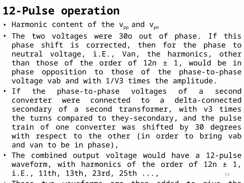
12-Pulse operation• Harmonic content of the vpp and vpn
• The two voltages were 30o out of phase. If this phase shift is corrected, then for the phase to neutral voltage, i.E., Van, the harmonics, other than those of the order of 12n ± 1, would be in phase opposition to those of the phase-to-phase voltage vab and with 1/V3 times the amplitude.
• If the phase-to-phase voltages of a second converter were connected to a delta-connected secondary of a second transformer, with v3 times the turns compared to they-secondary, and the pulse train of one converter was shifted by 30 degrees with respect to the other (in order to bring vab and van to be in phase),
• The combined output voltage would have a 12-pulse waveform, with harmonics of the order of 12n ± 1, i.E., 11th, 13th, 23rd, 25th ...,
• These two waveforms are then added to give the third waveform, which is seen to be a 12-pulse waveform, closer to being a sine wave than each of the six-pulse waveform.
• Two six-pulse converters, involving a total of six phase-legs are connected in parallel on the same de bus, and work together as a 12-pulse converter.

54
Current Source Conversion• A current-sourced converter is characterized by the fact that the
dc current flow is always in one direction and the power flow reverses with the reversal of dc voltage.(devices- diode, thyristor, turn-off device)
• It differs from the voltage-sourced converter in which the dc voltage always has one polarity and the power reversal takes place with reversal of dc current.(devices-turn-off device & reverse diode)

55
CSC – Diode converter• Which simply converts ac voltage to dc voltage,• Utilizes ac system voltage for commutation of dc current from one
valve to another. • Just converts ac power to dc power without any control• Consumes some reactive power on the ac side

56
CSC – Line-Commutated Converter• Based on conventional thyristors (with gate turn-on but without gate
turn-off capability)• Utilizes ac system voltage for commutation of current from one
valve to another• Convert and control active power in either direction• Consumes reactive power on the ac side. • It can not supply reactive power to the ac system.
57
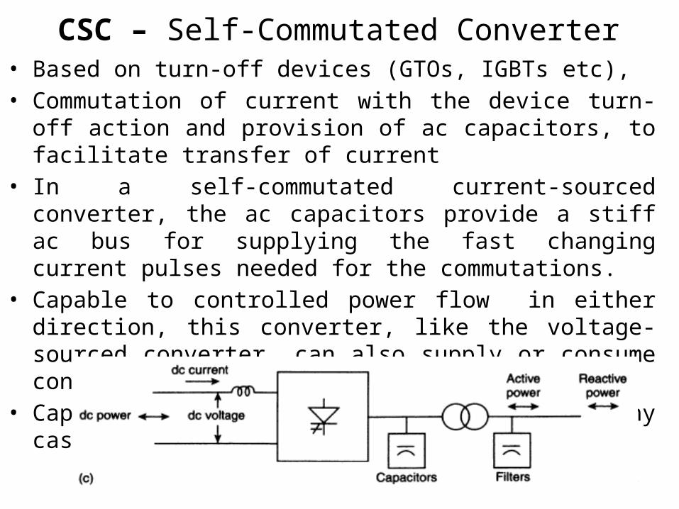
CSC – Self-Commutated Converter• Based on turn-off devices (GTOs, IGBTs etc), • Commutation of current with the device turn-off action and
provision of ac capacitors, to facilitate transfer of current• In a self-commutated current-sourced converter, the ac capacitors
provide a stiff ac bus for supplying the fast changing current pulses needed for the commutations.
• Capable to controlled power flow in either direction, this converter, like the voltage-sourced converter, can also supply or consume controlled reactive power.
• Capacitors and ac filters, are needed in any case.

58
CSC – Self-Commutated Converter• When reactive power management is not a problem and
the reactive power consumed by the converters can be supplied from the system capacitors and/or filters, the line-commutated converters have a decisive economic advantage over self-commutated converters
• DC voltage in a CSC can be in either direction,• Converter valves must have both forward and reverse
blocking capability. Thyristors are usually made as symmetric devices, i.e., They have both the forward and reverse blocking capability
• Easier and cheaper to make and can be made with peak blocking voltage as high as 12 kv along with a high current carrying capability

59
Three-phase full wave six-pulse diode converter• It is assumed that the dc side inductance is very large and therefore
the de current is constant• The circuit consists of six valves, numbered 1 to 6, the number
sequence conveying the order of the current transfer and the dc output voltage
• The current commutates from valve to valve to turn it into an ac current

60
Three-phase full wave six-pulse diode converter• 1or 3 or 5 conducts when Va,
Vb, Vc are most positive &
• 4 or 6 or 2 conducts when Va or Vb or Vc are most negative
• After every 60o one commutation takes place alternately in upper and lower
• Each valve conducts for 120o
• The current is made up of 120 degree blocks of dc current, through an upper and a lower valve of each phase leg

61
Three-phase full wave six-pulse diode converter• Commutation takes place from
valve to valve among valves connected to the same de bus, i.e., Valves 1 to 3 to 5 to 1 and
• Waveforms of ac current of a three-phase CSC are made up of 120o blocks and do not have triplen harmonics (VSC 180o)
• DC output voltage, i.e. the voltage of the positive pole with respect to the negative pole
• Ripple varying at 6 times the main frequency

62
Three-phase full wave six-pulse diode converter• The dc output voltage has a six-pulse waveform, made up of the
sum of two three-phase, half-wave circuits• The dc output voltage is made up of 60o segments and with the peak
of ac voltage as • E is the phase-to-phase voltage. • Output voltage is given by
• The output voltage is positive with dc current flowing out of the anode bus of the converter; hence the power flow is from ac to de (rectifier).
• DC output voltage contains some harmonics.

63
Three-phase full wave six-pulse diode converter• The ac current is made up of square wave blocks of 120 degree
duration each half-cycle. • The rms value of this phase current is given by
• Equating the fundamental ac power and the de power (neglecting losses),
• Substituting Vd in terms of E gives the rms fundamental ac current
• Total rms harmonic current

64
Three-phase full wave six-pulse diode converter
• There was one simplifying assumption in the above discussion that the current instantaneously commutated from one valve to another
• In reality it will take a significant time.• Typically it may take about 20 degrees to 30
degrees.• The commutation of in-line commutated
converters involves transfer of current from one phase to another through the valves in an inductive circuit of the ac system,

65
The commutation process• Presence of reactance • During the commutation, the magnetic
energy stored in the reactance of the previously conducting phase has to be transferred to the reactance of the incoming phase
• The commutation from valve 1 to valve 3 • any time after the upper voltage crossing
between vCR and vCY.
• Beyond that point vCY > vCR
• ic = i3 builds up at the expense of i1
• At all times i1+i3= Id,
• If the commutation reactances are balanced, the rates of change of i3 and −i1 are equal;
• therefore, the voltage drops across XCR and XCY are the same
• during the overlap period, the direct voltage vd is the mean value of vCY and vCR.

66
The commutation process

67
Three-phase full wave six-pulse diode converter• At t3, Valve 3 becomes FB &
starts to conduct with valve 1 carrying the full de current.
• The conducting of both valves 1 & 3 gives a short circuit between phases a and b with the short-circuit current rising from phase b through valve 3 into phase a through valve 1.
• Once the short-circuit current equals the de current through valve 1, its net current reaches zero, valve 1 stops conducting and the commutation is complete.
• Period of commutation, angle γo,

68
THYRISTOR-BASED CONVERTER• At

69
Three-phase full wave six-pulse diode converter• The short-circuit current between the
two phases for this period of commutation
• Assuming that when is = id, wt = γo
• Output voltage is reduced compared• During commutation, output follows
the mean of the two short-circuited voltages.
• The lost voltage corresponds to the shaded area every 60 degrees and is given by
• DC voltage drop in the converter due to the commutation of dc current

Three-phase full wave six-pulse diode converter• DC voltage drop is directly proportional to Id
• the current is shifted to the right by the commutation process. • the ac side power factor is reduced from unity to a lower value (lag), • that some reactive power is consumed.• This power factor reduction corresponds to the reduction in the dc
voltage. Equating the dc and ac power
• Combibe with Vo=1.35E and I1=0.78Id
• For practical estimation, power factor angle φ may be taken as

THYRISTOR-BASED CONVERTER• if the devices had a turn-on control, the start of each commutation
could be delayed and hence the output voltage reduced or even reversed at will.

72
No Delay in firing of valve
• Delaying the firing instants of the valves with respect to the voltage crossings, • The commencement of the natural commutations

73
Effect of firing delay on voltage waveforms:• Delaying the firing, the commencement of the natural commutations can be
delayed by a definite time interval• Voltage area, and the mean dc are reduced proportionally to the magnitude of the
delay• Large smoothing reactor on the DC side, the voltage waveform of will produce
constant DC

THYRISTOR-BASED CONVERTER