chapter 3 combinational logic design...chapter 3 - part 1 4 combinational circuits a combinational...
TRANSCRIPT
Charles Kime & Thomas Kaminski
© 2008 Pearson Education, Inc.
(Hyperlinks are active in View Show mode)
Chapter 3 – Combinational
Logic Design
Part 1 – Implementation Technology and Logic
Design
Logic and Computer Design Fundamentals

Updated by thoroughly by Dr. Waleed Dweik
Chapter 3 - Part 1 2

Chapter 3 - Part 1 3
Overview
Part 1 – Design Procedure
• Steps
Specification
Formulation
Optimization
Technology Mapping
Verification
• Technology Mapping - AND, OR, and NOT to NAND
or NOR

Chapter 3 - Part 1 4
Combinational Circuits
A combinational logic circuit has:
• A set of m Boolean inputs,
• A set of n Boolean outputs, and
• n switching functions, each mapping the 2m input
combinations to an output such that the current output
depends only on the current input values
A block diagram:

Chapter 3 - Part 1 5
Design Procedure
1. Specification
• Write a specification for the circuit if one is not already available. What does the circuit do? Including names or symbols for inputs and outputs
2. Formulation
• Derive a truth table or initial Boolean equations that define the required relationships between the inputs and outputs, if not in the specification
3. Optimization
• Apply 2-level optimization using K-maps
• Draw a logic diagram for the resulting circuit using ANDs, ORs, and inverters

Chapter 3 - Part 1 6
Design Procedure
4. Technology Mapping
• Map the logic diagram to the implementation
technology selected
5. Verification
• Verify the correctness of the final design
manually or using simulation

Design Example1
Specification: Design a combinational circuit that has 3
inputs (X, Y, Z) and one output F, such that 𝐹 = 1 when
the number of 1’s in the input is greater than the number of
0’s (i.e. number of 1’s ≥ 2)
• This is called majority function (i.e. majority of inputs must be 1
for the function to be 1)
Formulation:
Chapter 3 - Part 1 7
X Y Z F
0 0 0 0
0 0 1 0
0 1 0 0
0 1 1 1
1 0 0 0
1 0 1 1
1 1 0 1
1 1 1 1

Design Example1 Cont.
Optimization:
𝐹 𝑋, 𝑌, 𝑍 = 𝑋𝑌 + 𝑋𝑍 + 𝑌𝑍
Technology Mapping:
• Mapping with a library containing inverters, 2-input AND, 2-input
OR
Chapter 3 - Part 1 8
𝒀
0
1
3
1 2
𝑿 4
5
1 7
1 6
1
𝒁
X
Z
X
Y
Y
Z
F

Design Example2
Specification: Design a combinational
circuit that compares 2-bit Binary number
(A, B) and produce two outputs (O1, O0),
such that:
Formulation:
Chapter 3 - Part 1 9
A(A1A0) B(B1B0) O(O1O0)
00 00 00
00 01 01
00 10 01
00 11 01
01 00 10
01 01 11
01 10 01
01 11 01
10 00 10
10 01 10
10 10 00
10 11 01
11 00 10
11 01 10
11 10 10
11 11 11
𝑶𝟏𝑶𝟎 = 𝟎𝟎 When 𝑨 = 𝑩 𝒂𝒏𝒅 𝑩𝒐𝒕𝒉 𝒂𝒓𝒆 𝒆𝒗𝒆𝒏
𝑶𝟏𝑶𝟎 = 𝟎𝟏 When 𝑨 < 𝑩
𝑶𝟏𝑶𝟎 = 𝟏𝟎 When 𝑨 > 𝑩
𝑶𝟏𝑶𝟎 = 𝟏𝟏 When 𝑨 = 𝑩 𝒂𝒏𝒅 𝑩𝒐𝒕𝒉 𝒂𝒓𝒆 𝒐𝒅𝒅

Design Example2 Cont.
Optimization and Technology Mapping:
𝑂0 = 𝐵1𝐵0 + 𝐴1𝐵1 + 𝐴1𝐵0
𝑂1 = 𝐴1𝐴0 + 𝐴0𝐵1 + 𝐴1𝐵1
Chapter 3 - Part 1 10
𝑩𝟏
0
1
1
3
1
2
1
4
5
1
7
1
6
1 𝑨𝟎
𝑨𝟏
12
13
15
1
14
8
9
11
1
10
𝑩𝟎
O0
𝑩𝟏
0
1
3
2
4
1
5
1
7
6
𝑨𝟎
𝑨𝟏
12
1
13
1
15
1
14
1
8
1
9
1
11
10
𝑩𝟎
O1

Chapter 3 - Part 1 11
Design Example3
1. Specification
• BCD to Excess-3 code converter
• Transforms BCD code for the decimal digits to Excess-3 code for the decimal digits
• BCD code words for digits 0 through 9: 4-bit patterns 0000 to 1001, respectively
• Excess-3 code words for digits 0 through 9: 4-bit patterns consisting of 3 (binary 0011) added to each BCD code word
• BCD input is labeled A, B, C, D
• Excess-3 output is labeled W, X, Y, Z

Chapter 3 - Part 1 12
Design Example3 Cont.
2. Formulation
ABCD WXYZ
0000 0011
0001 0100
0010 0101
0011 0110
0100 0111
0101 1000
0110 1001
0111 1010
1000 1011
1001 1100
1010 XXXX
1011 XXXX
1100 XXXX
1101 XXXX
1110 XXXX
1111 XXXX

Design Example3 Cont.
3. Optimization
𝑊 = 𝐴 + 𝐵𝐶 + 𝐵𝐷
𝑋 = 𝐵 𝐷 + 𝐵 𝐶 + 𝐵𝐶 𝐷
𝑌 = 𝐶 𝐷 + 𝐶𝐷
𝑍 = 𝐷
𝑪
0
1
3
2
4
5
1
7
1
6
1 𝑩
𝑨
12
X
13
X
15
X
14
X
8
1
9
1
11
X
10
X
𝑫
W
𝑪
0
1
1
3
2
1
4
1
5
7
6
1 𝑩
𝑨
12
X
13
X
15
X
14
X
8
1
9
11
X
10
X
𝑫
Z
Chapter 3 - Part 1 13
𝑪
0
1
1
3
1
2
4
1
5
7
1
6
𝑩
𝑨
12
X
13
X
15
X
14
X
8
1
9
11
X
10
X
𝑫
𝑪
0
1
1
3
1
2
1
4
1
5
7
6
𝑩
𝑨
12
X
13
X
15
X
14
X
8
9
1
11
X
10
X
𝑫
X
Y

Chapter 3 - Part 1 14
Design Example3 Cont.
4. Technology Mapping • Mapping with a library containing inverters, 2-input AND,
2-input OR B
C
D
C
W
BA
B
D
C
D
B
X
Z
C
D
Y

Homework: BCD to 7-Segment
Specification:
• Inputs: (A, B, C, D) BCD code from 0000-to-1001
• Outputs: (g, f, e, d, c, b, a)
Formulation:
Optimization:
• How many
K-maps?
Chapter 3 - Part 1 15
A B C D g f e d c b a
0 0 0 0 0 1 1 1 1 1 1
0 0 0 1 0 0 0 0 1 1 0
|
|
|
|
|
1 0 0 1 1 1 0 0 1 1 1
1 0 1 0 0 0 0 0 0 0 0
|
|
|
|
|
1 1 1 1 0 0 0 0 0 0 0

Chapter 3 - Part 1 16
Technology Mapping
Mapping Procedures
• To NAND gates
• To NOR gates

Chapter 3 - Part 1 17
Mapping to NAND gates
Assumptions:
• Gate loading and delay are ignored
• Cell library contains an inverter and n-input NAND
gates, n = 2, 3, …
• An AND, OR, inverter schematic for the circuit is
available
The mapping is accomplished by:
• Replacing AND and OR symbols,
• Pushing inverters through circuit fan-out points,
and
• Canceling inverter pairs

Chapter 3 - Part 1 18
NAND Mapping Algorithm
1. Replace ANDs and ORs:
2. Repeat the following pair of actions until there
is at most one inverter between :
a. A circuit input or driving NAND gate output, and
b. The attached NAND gate inputs.
.
.
....
.
.
.
.
.
.
.
.
....

Chapter 3 - Part 1 19
NAND Mapping Example

Chapter 3 - Part 1 20
Mapping to NOR gates
Assumptions:
• Gate loading and delay are ignored
• Cell library contains an inverter and n-input NOR
gates, n = 2, 3, …
• An AND, OR, inverter schematic for the circuit is
available
The mapping is accomplished by:
• Replacing AND and OR symbols,
• Pushing inverters through circuit fan-out points,
and
• Canceling inverter pairs

Chapter 3 - Part 1 21
NOR Mapping Algorithm
1. Replace ANDs and ORs:
2. Repeat the following pair of actions until there
is at most one inverter between :
a. A circuit input or driving NAND gate output, and
b. The attached NAND gate inputs.
.
.
....
.
.
.
.
.
....
.
.
.
Chapter 3 - Part 1 22
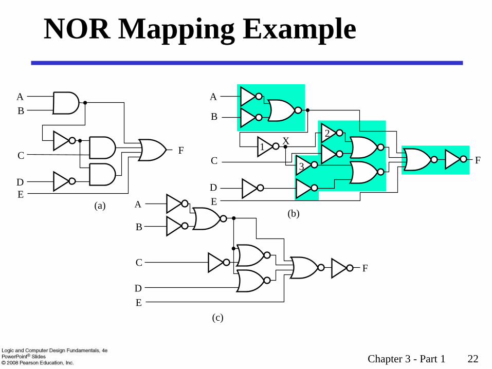
NOR Mapping Example
A
B
C
D
E
F
(c)
F
A
B
X
C
D
E
(b)
A
B
C
D
E
F
(a)
2
3
1

Chapter 3 - Part 1 23
Terms of Use
All (or portions) of this material © 2008 by Pearson Education, Inc.
Permission is given to incorporate this material or adaptations thereof into classroom presentations and handouts to instructors in courses adopting the latest edition of Logic and Computer Design Fundamentals as the course textbook.
These materials or adaptations thereof are not to be sold or otherwise offered for consideration.
This Terms of Use slide or page is to be included within the original materials or any adaptations thereof.

Charles Kime & Thomas Kaminski
© 2008 Pearson Education, Inc. (Hyperlinks are active in View Show mode)
Chapter 3 – Combinational
Logic Design
Part 2 – Combinational Logic
Logic and Computer Design Fundamentals

Updated Thoroughly by Dr. Waleed Dweik
Chapter 3 2

Chapter 3 3
Overview
Part 2 – Combinational Logic
• Functions and functional blocks
• Rudimentary logic functions
• Decoding using Decoders
Implementing Combinational Functions with Decoders
• Encoding using Encoders
• Selecting using Multiplexers
Implementing Combinational Functions with Multiplexers

Chapter 3 4
Functions and Functional Blocks
The functions considered are those found to be very
useful in design
Corresponding to each of the functions is a
combinational circuit implementation called a
functional block
In the past, functional blocks were packaged as
small-scale-integrated (SSI), medium-scale
integrated (MSI), and large-scale-integrated (LSI)
circuits
Today, they are often simply implemented within a
very-large-scale-integrated (VLSI) circuit

Rudimentary Logic Functions
Functions of a single variable X
Can be used on the
inputs to functional
blocks to implement
other than the block’s
intended function
Value fixing : a, b
Transferring : c
Inverting : d
Enabling : next slide
Chapter 3 5
0
1
F = 0
F = 1
(a)
F = 0
F = 1
V CC or V DD
(b)
X F = X
(c)
X F = X
(d)
Functions of One Variable
𝑿 𝑭 = 𝟎 𝑭 = 𝟏 𝑭 = 𝑿 𝑭 = 𝑿
0 0 1 0 1
1 0 1 1 0
Chapter 3 6
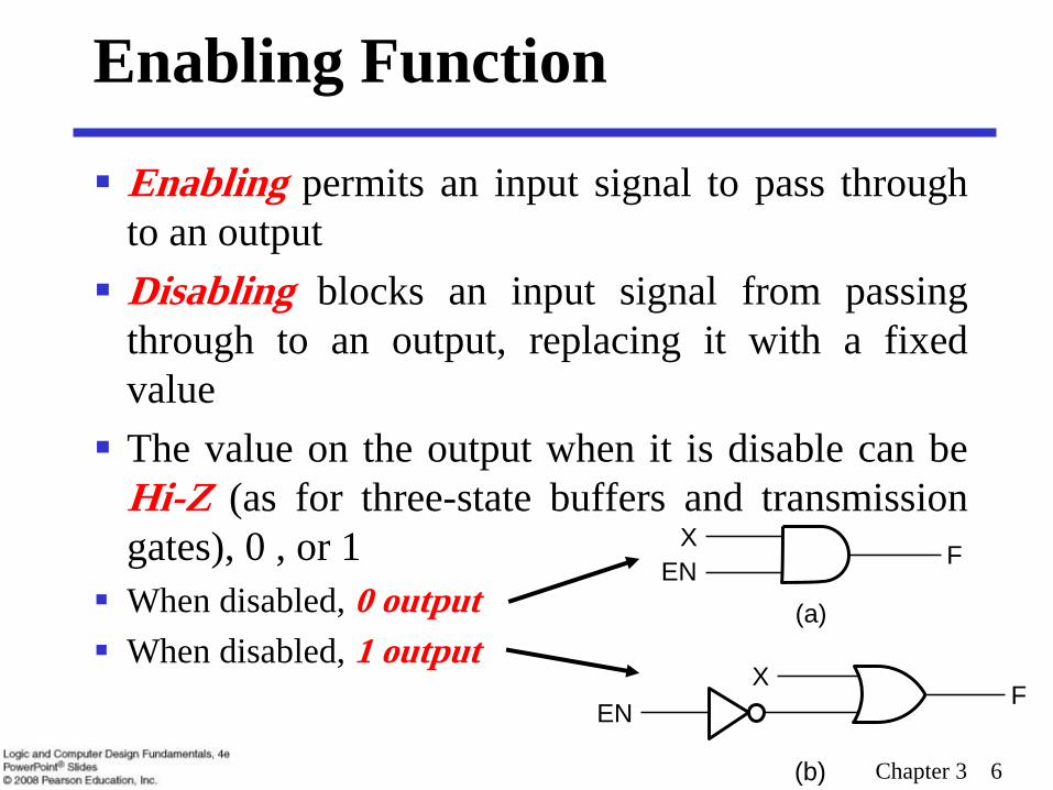
Enabling Function
Enabling permits an input signal to pass through
to an output
Disabling blocks an input signal from passing
through to an output, replacing it with a fixed
value
The value on the output when it is disable can be
Hi-Z (as for three-state buffers and transmission
gates), 0 , or 1
When disabled, 0 output
When disabled, 1 output
XF
EN
(a)
EN
XF
(b)

Chapter 3 7
Decoding: the conversion of an n-bit input code to an
m-bit output code with n m 2n such that each
valid code word produces a unique output code
Circuits that perform decoding are called decoders
Functional blocks for decoding are
• called n-to-m line decoders, where m 2n, and
• generate 2n (or fewer) minterms for the n input variables
Decoding

1-to-2 Line Decoder
When the decimal value of A equals the subscript of 𝐷𝑖, that 𝐷𝑖 will be 1 and all others will be 0’s
Only one output is active at a time
Decoders are used to control multiple circuits by enabling
only one of them at a time
Chapter 3 8
A D 0 D 1
0 1 0
1 0 1
(a) (b)
D 1 = A A
D 0 = A 1-to-2
Decoder A
𝐷0
𝐷1
(c)

2-to-4 Line Decoder
No more optimization is possible
Note that the 2-to-4 line decoder is made up of two 1-
to-2- line decoders and 4 AND gates
Chapter 3 9
A 1
0
0
1
1
A 0
0
1
0
1
D 0
1
0
0
0
D 1
0
1
0
0
D 2
0
0
1
0
D 3
0
0
0
1
(a)
D 0 = A 1
A 0
D 1 = A 1
A 0
D 2 = A 1
A 0
D 3 = A 1
A 0
(b)
A 1
A 0
2-to-4
Decoder
𝐴0 𝐷0
𝐷1
(c)
𝐴1 𝐷2
𝐷3

Chapter 3 10
Decoder Expansion
General procedure given in book for any decoder with n
inputs and 2n outputs
This procedure builds a decoder backward from the outputs
using
1. Let k = n
2. We need 2k 2-input AND gates driven as follows:
If k is even, drive the gates using two k/2-to-2k/2 decoders
If k is odd, drive the gates using one (k+1)/2-to-2(k+1)/2
decoder and one (k-1)/2-to-2(k-1)/2 decoder
3. For each decoder resulting from step2, repeat
step2 until k = 1. For k = 1, use 1-to-2 decoder

Chapter 3 11
Decoder Expansion - Example 1
3-to-8-line decoder
• 𝑘 = 𝑛 = 3
• We need 23(8) 2-input AND gates driven as follows:
• 𝑘 is odd, so split to:
2-to-4-line decoder
1-to-2-line decoder
• 2-to-4-line decoder 𝑘 = 𝑛 = 2 We need 22(4) 2-input AND gates driven as follows:
𝑘 is even, so split to:
• Two 1-to-2-line decoder
See next slide for result

Chapter 3 12
Decoder Expansion - Example 1
𝑮𝑵 = 𝟖 × 𝟐 + 𝟒 × 𝟐 + 𝟑
𝑮𝑵 = 𝟐𝟕
Straight forward design
has the same GN cost

Chapter 3 13
Decoder Expansion - Example 2
6-to-64-line decoder
• 𝑘 = 𝑛 = 6
• We need 26(64) 2-input AND gates driven as follows:
• 𝑘 is even, so split to:
Two 3-to-8-line decoders
• Each 3-to-8-line decoder is designed as shown in Example 1

Decoder Expansion - Example 2
𝑮𝑵 = 𝟔𝟒 × 𝟐 + 𝟏𝟔 × 𝟐 + 𝟖 × 𝟐 + 𝟔
𝑮𝑵 = 𝟏𝟖𝟐
Straight forward design has
GN cost of 390
Chapter 3 14
𝐴0
𝐴1
𝐴2
𝐴3
𝐴4
𝐴5
𝐷0 = 𝐴5 𝐴4 𝐴3 𝐴2 𝐴1 𝐴0
𝐷1 = 𝐴5 𝐴4 𝐴3 𝐴2 𝐴1𝐴0
𝐷63 = 𝐴5𝐴4𝐴3𝐴2𝐴1𝐴0
𝐷62 = 𝐴5𝐴4𝐴3𝐴2𝐴1𝐴0

Chapter 3 15
Decoder Expansion - Example 3
7-to-128-line decoder
• 𝑘 = 𝑛 = 7
• We need 27(128) 2-input AND gates driven as follows:
• 𝑘 is odd, so split to:
4-to-16-line decoder
3-to-8-line decoder
• 4-to-16-line decoder
𝑘 = 𝑛 = 4
We need 24(16) 2-input AND gates driven as follows:
𝑘 is even, so split to:
• Two 2-to-4-line decoders
• Complete using known 3-8 and 2-to-4 line decoders
𝐺𝑁 = 128 × 2 + 16 × 2 + 8 × 2 + 12 × 2 + 7 = 335
Compare to straight forward design with GN cost of 903

Building Larger Decoders
Method_1: Decoder Expansion
Method_2: Using Small Decoders with Enable input
Example: 1-to-2 line decoder with enable
• In general, attach m-enabling circuits to the outputs
• See truth table below for function
Note use of X’s to denote both 0 and 1
Combination containing two X’s represent two binary combinations
Alternatively, can be viewed as distributing value of signal EN to 1 of 2
outputs
• In this case, it is called a Demultiplexer
Chapter 3 16
A D 0 D 1
0 1 0
1 0 1
(a) (b)
D 1 A
D 0 1-to-2
Decoder A
𝐷0
𝐷1
(c)
EN
1
1
X 0 0 0
EN
EN

Chapter 3 17
Attach 4-enabling circuits to the outputs
See truth table below for function
• Combination containing two X’s represent four binary combinations
Alternatively, can be viewed as distributing value of signal EN to 1 of 4
outputs
• In this case, it is called a Demultiplexer EN
A 1
A 0
D0
D1
D2
D3
(b)
EN A1 A0 D0 D1 D2 D3
0
1
1
1
1
X
0
0
1
1
X
0
1
0
1
0
1
0
0
0
0
0
1
0
0
0
0
0
1
0
0
0
0
0
1
(a)
2-to-4 Line Decoder with Enable
2-to-4
Decoder
𝐴0 𝐷0 𝐷1
𝐴1 𝐷2 𝐷3
𝐸𝑁
(c)

2-to-4 Decoder using 1-to-2 Decoders and Inverters
𝑨𝟏 𝑨𝟎 𝑫𝟎 𝑫𝟏 𝑫𝟐 𝑫𝟑
0 0 1 0 0 0
0 1 0 1 0 0
1 0 0 0 1 0
1 1 0 0 0 1
1st 1-to-2 Decoder 2nd 1-to-2 Decoder
Chapter 3 18

3-to-8 Decoder using 2-to-4 Decoders and Inverters
𝑨𝟐 𝑨𝟏 𝑨𝟎 𝑫𝟎 𝑫𝟏 𝑫𝟐 𝑫𝟑 𝑫𝟒 𝑫𝟓 𝑫𝟔 𝑫𝟕
0 0 0 1 0 0 0 0 0 0 0
0 0 1 0 1 0 0 0 0 0 0
0 1 0 0 0 1 0 0 0 0 0
0 1 1 0 0 0 1 0 0 0 0
1 0 0 0 0 0 0 1 0 0 0
1 0 1 0 0 0 0 0 1 0 0
1 1 0 0 0 0 0 0 0 1 0
1 1 1 0 0 0 0 0 0 0 1
1st 2-to4 Decoder 2nd 2-to4 Decoder
Chapter 3 19

4-to-16 Decoder using Only 2-to-4 Decoders
Chapter 3 20

Chapter 3 21
Combinational Logic Implementation
- Decoder and OR Gates
Implement m functions of n variables with:
• Sum-of-minterms expressions
• One n-to-2n-line decoder
• m OR gates, one for each function
• For each function, the OR gate has k inputs, where k is the number
of minterms in the function
Approach 1:
• Find the truth table for the functions
• Make a connection to the corresponding OR from the
corresponding decoder output wherever a 1 appears in the truth
table
Approach 2
• Find the minterms for each output function
• OR the minterms together

Example1
Implement function 𝑓 using decoder and OR gate: 𝒇 𝒙, 𝒚, 𝒛 = 𝒙𝒛 + 𝒙 𝒚
𝑛 = 3 variables 3-to-8 decoder
One function One OR gate
Solution: Convert 𝑓 to SOM format
•𝑓 = 𝑥𝑧 𝑦 + 𝑦 + 𝑥 𝑦 𝑧 + 𝑧 = 𝑥𝑦𝑧 + 𝑥𝑦 𝑧 + 𝑥 𝑦𝑧 + 𝑥 𝑦𝑧
•𝑓 𝑥, 𝑦, 𝑧 = (2,3,4,6)𝑚 4-input OR gate
Decoder is a Minterm
Generator
Chapter 3 22

Example2
Implement function 𝑓 using decoder and OR gate:
𝒇 𝒘, 𝒙, 𝒚, 𝒛 = (𝟎, 𝟒, 𝟖, 𝟏𝟏, 𝟏𝟐, 𝟏𝟒, 𝟏𝟓)
𝒎
𝑛 = 4 variables 4-to-16 decoder
One function with 7 minterms One 7-input OR gate
If number of minterms is greater
than 𝟐𝒏
𝟐 , then design for
complement F (𝑭 ) and use NOR
gate instead of OR to generate F
Chapter 3 23

Example3
Implement functions 𝐶 𝑎𝑛𝑑 𝑆 using decoder and OR gates:
𝑛 = 3 variables 3-to-8 decoder
Two function Two OR gates
Solution:
• 𝐶 = (3,5,𝑚 6,7) 4-input OR gate
• 𝑆 = (1,2,4,7)𝑚 4-input OR gate
Chapter 3 24
𝑿 𝒀 𝒁 𝑪 𝑺
0 0 0 0 0
0 0 1 0 1
0 1 0 0 1
0 1 1 1 0
1 0 0 0 1
1 0 1 1 0
1 1 0 1 0
1 1 1 1 1

Chapter 3 25
Example4
Implement the following set of odd parity functions of
(A7, A6, A5, A4)
P1 = A7 A5 A4
P2 = A7 A6 A4
P3 = A7 A6 A5
Finding sum of
minterms expressions
P1 = Sm(1,2,5,6,8,11,12,15)
P2 = Sm(1,3,4,6,8,10,13,15)
P3 = Sm(2,3,4,5,8,9,14,15)
Find circuit
Is this a good idea?
+
+
+
+
+
+
0
1
2
3
4
5
6
7
8
9
10
11
12
13
14
15
A4
A5
A6
A7
P1
P3
P2
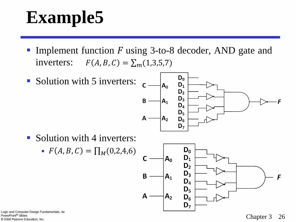
Example5
Implement function 𝐹 using 3-to-8 decoder, AND gate and
inverters: 𝐹 𝐴, 𝐵, 𝐶 = (1,3,5,7)𝑚
Solution with 5 inverters:
Solution with 4 inverters:
• 𝐹 𝐴, 𝐵, 𝐶 = (0,2,4,6)𝑀
Chapter 3 26

Chapter 3 27
Encoding
Encoding: the opposite of decoding - the conversion of
an m-bit input code to a n-bit output code with n m
2n such that each valid code word produces a unique
output code
Circuits that perform encoding are called encoders
An encoder has 2n (or fewer) input lines and n output
lines which generate the binary code corresponding to
the input values
Typically, an encoder converts a code containing exactly
one bit that is 1 to a binary code corresponding to the
position in which the 1 appears

2-to-1 Encoder & 4-to-2 Encoder
Chapter 3 28
2-to-1
Encoder A
𝐷0
𝐷1
(c) (a) (b)
𝑨 𝑫𝟎 𝑫𝟏
Invalid Input 0 0
0 1 0
1 0 1
Invalid Input 1 1
4-to-2
Encoder
𝐷0
𝐷1
(c) (a)
(b)
𝑨𝟎 𝑨𝟏 𝑫𝟎 𝑫𝟏 𝑫2 𝑫3
0 0 1 0 0 0
1 0 0 1 0 0
0 1 0 0 1 0
1 1 0 0 0 1
𝐷2
𝐷3
𝐴0
𝐴1
𝐴 = 𝐷1. 𝐷0
𝐴0 = 𝐷1 + 𝐷3
𝐴1 = 𝐷2 + 𝐷3
D1
D0
A
`

8-to-3 Encoder (Octal-to-Binary Encoder)
Chapter 3 29
8-to-3
Encoder
𝐷0
𝐷1
(c)
(a)
(b)
𝑨𝟎 𝑨𝟏 𝑨𝟐 𝑫𝟎 𝑫𝟏 𝑫2 𝑫3 𝑫4 𝑫5 𝑫6 𝑫7
0 0 0 1 0 0 0 0 0 0 0
1 0 0 0 1 0 0 0 0 0 0
0 1 0 0 0 1 0 0 0 0 0
1 1 0 0 0 0 1 0 0 0 0
0 0 1 0 0 0 0 1 0 0 0
1 0 1 0 0 0 0 0 1 0 0
0 1 1 0 0 0 0 0 0 1 0
1 1 1 0 0 0 0 0 0 0 1
𝐷2
𝐷3
𝐴0
𝐴1
𝐴0 = 𝐷1 + 𝐷3 + 𝐷5 + 𝐷7
𝐴1 = 𝐷2 + 𝐷3 + 𝐷6 + 𝐷7
𝐷4
𝐷5
𝐷6
𝐷7
𝐴2
𝐴2 = 𝐷4 + 𝐷5 + 𝐷6 + 𝐷7

Chapter 3 30
Decimal-to-BCD Encoder
Inputs: 10 bits corresponding to decimal digits 0
through 9, (D0, …, D9)
Outputs: 4 bits with BCD codes (A3, A2, A1, A0)
Function: If input bit Di is a 1, then the output is
the BCD code for i
The truth table could be formed, but alternatively,
the equations for each of the four outputs can be
obtained directly

Chapter 3 31
Decimal-to-BCD Encoder Cont.
Input Di is a term in equation Aj if bit Aj is 1 in the binary value
for i
Equations:
A3 = D8 + D9
A2 = D4 + D5 + D6 + D7
A1 = D2 + D3 + D6 + D7
A0 = D1 + D3 + D5 + D7 + D9
What happens if two inputs are high simultaneously?
• For example if D3 and D6 are high, then the output is 0111 which
indicates that only D7 is high ???
• Solution: Establish input priority

Chapter 3 32
Priority Encoder
If more than one input value is 1, then the encoder just designed does
not work
One encoder that can accept all possible combinations of input values
and produce a meaningful result is a priority encoder
Among the 1s that appear, it selects the most significant input position
(or the least significant input position) containing a 1 and responds with
the corresponding binary code for that position
• High priority encoder: gives priority for the input whose value is 1 and
has the highest subscript
• low priority encoder: gives priority for the input whose value is 1 and has
the lowest subscript
If all inputs are 0’s, what happens?
• Define an output (V) to encode whether the input is valid or not
• When all inputs are 0’s, V is set to 0 indicating that the input is invalid,
otherwise V is set to 1
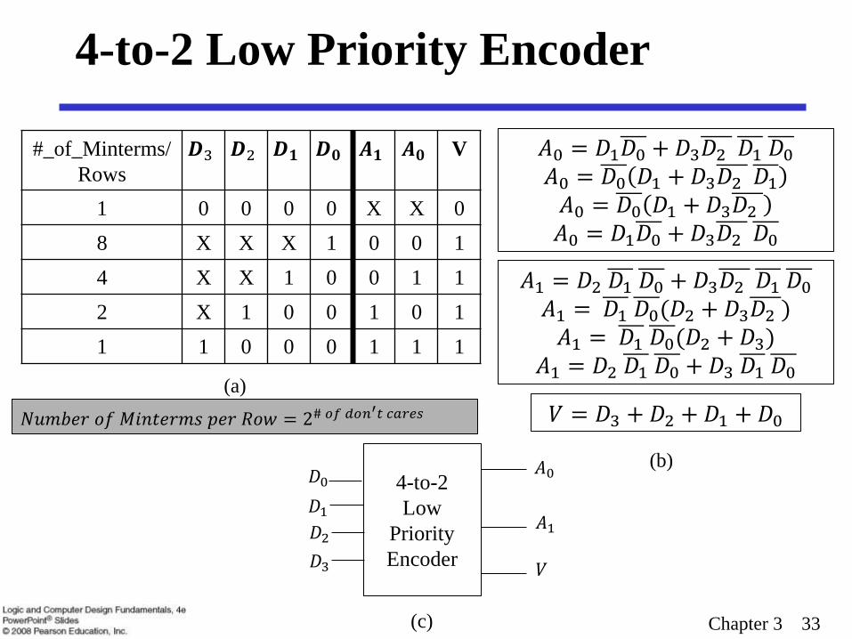
4-to-2 Low Priority Encoder
Chapter 3 33
4-to-2
Low
Priority
Encoder
𝐷0
𝐷1
(c)
(a)
(b)
V 𝑨𝟎 𝑨𝟏 𝑫𝟎 𝑫𝟏 𝑫2 𝑫3 #_of_Minterms/
Rows
0 X X 0 0 0 0 1
1 0 0 1 X X X 8
1 1 0 0 1 X X 4
1 0 1 0 0 1 X 2
1 1 1 0 0 0 1 1
𝐷2
𝐷3
𝐴0
𝐴1
𝐴0 = 𝐷1𝐷0 + 𝐷3𝐷2 𝐷1 𝐷0 𝐴0 = 𝐷0 𝐷1 + 𝐷3𝐷2 𝐷1 𝐴0 = 𝐷0 𝐷1 + 𝐷3𝐷2 𝐴0 = 𝐷1𝐷0 + 𝐷3𝐷2 𝐷0
𝐴1 = 𝐷2 𝐷1 𝐷0 + 𝐷3𝐷2 𝐷1 𝐷0 𝐴1 = 𝐷1 𝐷0(𝐷2 + 𝐷3𝐷2 ) 𝐴1 = 𝐷1 𝐷0(𝐷2 + 𝐷3) 𝐴1 = 𝐷2 𝐷1 𝐷0 + 𝐷3 𝐷1 𝐷0
𝑉 = 𝐷3 + 𝐷2 + 𝐷1 + 𝐷0
𝑉
𝑁𝑢𝑚𝑏𝑒𝑟 𝑜𝑓 𝑀𝑖𝑛𝑡𝑒𝑟𝑚𝑠 𝑝𝑒𝑟 𝑅𝑜𝑤 = 2# 𝑜𝑓 𝑑𝑜𝑛′𝑡 𝑐𝑎𝑟𝑒𝑠

4-to-2 High Priority Encoder
Chapter 3 34
4-to-2
High
Priority
Encoder
𝐷0
𝐷1
(c)
(a)
(b)
V 𝑨𝟎 𝑨𝟏 𝑫𝟎 𝑫𝟏 𝑫2 𝑫3 #_of_Minterms/
Rows
0 X X 0 0 0 0 1
1 0 0 1 0 0 0 1
1 1 0 X 1 0 0 2
1 0 1 X X 1 0 4
1 1 1 X X X 1 8
𝐷2
𝐷3
𝐴0
𝐴1
𝐴0 = 𝐷3 + 𝐷3 𝐷2𝐷1 𝐴0 = 𝐷3 + 𝐷2𝐷1
𝐴1 = 𝐷3 + 𝐷3𝐷2 𝐴1 = 𝐷3 + 𝐷2
𝑉 = 𝐷3 + 𝐷2 + 𝐷1 + 𝐷0
𝑉

Chapter 3 35
5-input Priority Encoder
Priority encoder with 5 inputs (D4, D3, D2, D1, D0) - highest priority to most
significant 1 present - Code outputs A2, A1, A0 and V where V indicates at
least one 1 present
X’s in input part of table represent 0 or 1; thus table entries correspond to
product terms instead of minterms. The column on the left shows that all 32
minterms are present in the product terms in the table
No. of Min-
terms/Row
Inputs Outputs
D4 D3 D2 D1 D0 A2 A1 A0 V
1 0 0 0 0 0 X X X 0
1 0 0 0 0 1 0 0 0 1
2 0 0 0 1 X 0 0 1 1
4 0 0 1 X X 0 1 0 1
8 0 1 X X X 0 1 1 1
16 1 X X X X 1 0 0 1

Chapter 3 36
5-input Priority Encoder Cont.
Could use a K-map to get equations, but can be read
directly from table and manually optimized if careful:
A2 = D4
A1 = D3 + D2 = (D3 + D2)
A1 = D3 + D2
A0 = D3 + D1 = (D3 + D1)
A0 = D3 + D1
V = D4 + D3 + D2 + D1 + D0
D4 D3 D4 D4
D4 D3 D4 D2 D4 D2
D4 D4
D4 D2 D4
Chapter 3 37
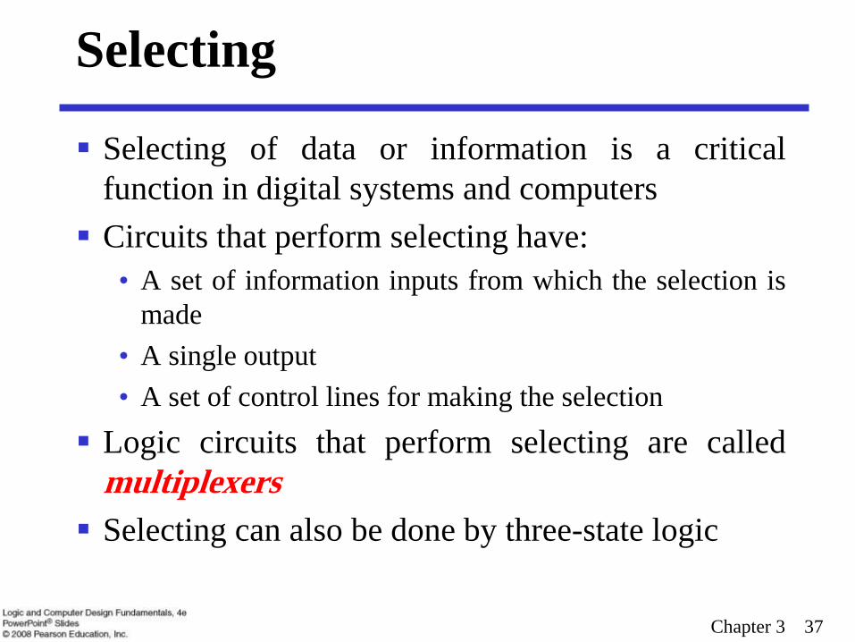
Selecting of data or information is a critical
function in digital systems and computers
Circuits that perform selecting have:
• A set of information inputs from which the selection is
made
• A single output
• A set of control lines for making the selection
Logic circuits that perform selecting are called
multiplexers
Selecting can also be done by three-state logic
Selecting

Chapter 3 38
Multiplexers (MUX) (Data Selectors)
A multiplexer selects information from an input line and
directs the information to an output line
A typical multiplexer has n control inputs (𝑆𝑛−1, … 𝑆0) called selection inputs, 2n information inputs (𝐼2𝑛−1, …
𝐼0), and one output Y
A multiplexer can be designed to have m information
inputs with m < 2n as well as n selection inputs
Multiplexers allow sharing of resources and reduce the cost
by reducing the number of wires
MUX 2𝑛
𝐼
𝑛
𝑆
𝑌

Chapter 3 39
2-to-1-Line MUX
Since 2 = 21, n = 1
The single selection
variable S has two
values:
• S = 0 selects input I0
• S = 1 selects input I1
The equation:
𝒀 = 𝑺 𝑰𝟎 + 𝑺𝑰𝟏
The circuit:
S
I0
I1
DecoderEnablingCircuits
Y
𝑺 𝑰𝟏 𝑰𝟎 𝒀
0 0 0 0
𝒀 = 𝑰𝟎 0 0 1 1
0 1 0 0
0 1 1 1
1 0 0 0
𝒀 = 𝑰𝟏
1 0 1 0
1 1 0 1
1 1 1 1
𝑺 𝒀
0 I0
1 I1
𝑰𝟏
0
1
1 3
1 2
𝑺 4
5 7
1 6
1
𝑰𝟎
2-to-1
MUX
𝐼0
𝑆
𝑌 𝐼1

Chapter 3 40
2-to-1-Line MUX Cont.
Note the regions of the multiplexer circuit
shown:
• 1-to-2-line Decoder
• 2 Enabling circuits
• 2-input OR gate
In general, for an 2n-to-1-line multiplexer:
• n-to-2n-line decoder
• 2n 2-input AND gate
• One 2n-input OR gate

4-to-1-Line MUX
Since 4 = 22, n = 2
There are two selection
variables (𝑺𝟏𝑺𝟎) and
they have four values:
• 𝑺𝟏𝑺𝟎 = 𝟎𝟎 selects input I0
• 𝑺𝟏𝑺𝟎 = 𝟎𝟏 selects input I1
• 𝑺𝟏𝑺𝟎 = 𝟏𝟎 selects input I2
• 𝑺𝟏𝑺𝟎 = 𝟏𝟏 selects input I3
The equation:
𝒀 = 𝑺𝟏 𝑺𝟎𝑰𝟎 + 𝑺𝟏 𝑺𝟎𝑰𝟏 + 𝑺𝟏𝑺𝟎 𝑰𝟐 + 𝑺𝟏𝑺𝟎𝑰𝟑
Chapter 3 41
𝑺𝟏 𝑺𝟎 𝒀
0 0 𝐈𝟎
0 1 𝐈𝟏
1 0 𝐈𝟐
1 1 𝐈𝟑
4-to-1
MUX
𝑆1
𝑌
𝑆0
𝐼0
𝐼1
𝐼2
𝐼3

Chapter 3 42
4-to-1-line MUX Cont.
2-to-4-line decoder
4 2-input AND gates
4-input OR gate
S 1
Decoder
S 0
Y
S 1
Decoder
S 0
Y
S 1
2-to-4 Decoder
4 2-input AND gates
4-input OR gate
S 0
Y
I 2
I 3
I 1
I 0
Y Y
Y
I 2
I 3
I 1
I 0
2-to-4
Decoder
𝑆0 𝐷0
𝐷1
𝑆1
𝐷2
𝐷3

Homework
Implement 8-to-1-Line MUX and 64-to-1
MUX:
• How many select lines are needed?
• Decoder size?
• How many 2-input AND gates are needed?
• What is the size of the OR gate?
Chapter 3 43
Chapter 3 44
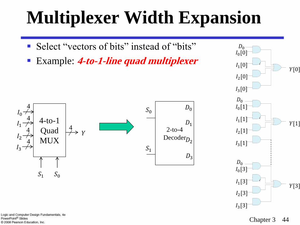
Multiplexer Width Expansion
Select “vectors of bits” instead of “bits”
Example: 4-to-1-line quad multiplexer
4-to-1
Quad
MUX
𝑆1
𝑌
𝑆0
𝐼0
𝐼1
𝐼2
𝐼3
4
4
4
4
4
2-to-4
Decoder
𝑆0 𝐷0
𝐷1
𝑆1
𝐷2
𝐷3
Y Y
𝐼0[0]
𝐼1[0]
𝐼2[0]
𝐼3[0]
𝑌[0]
Y Y
𝐼0[1]
𝐼1[1]
𝐼2[1]
𝐼3[1]
𝑌[1]
Y Y
𝐼0[3]
𝐼1[3]
𝐼2[3]
𝐼3[3]
𝑌[3]
𝐷0
𝐷0
𝐷0

Multiplexer Width Expansion Cont.
Can be thought
of as four 4-to-1
MUXes:
Chapter 3 45
4-to-1
MUX 𝑌[0]
𝐼0[0] 𝐼1[0]
𝐼2[0]
𝐼3[0]
4-to-1
MUX 𝑌[1]
𝐼0[1] 𝐼1[1]
𝐼2[1]
𝐼3[1]
4-to-1
MUX 𝑌[3]
𝐼0[3] 𝐼1[3]
𝐼2[3]
𝐼3[3]
𝑠1
𝑠0

Chapter 3 46
Other Selection Implementations
Three-state logic
I0
I1
I2
I3
S1
S0
(b)
Y

Building Large MUXes from Smaller Ones
4-to-1 MUX using
three 2-to-1 MUXes
6-to-1 MUX using
two 4-to-1 MUXes
and one 2-to-1 MUX
Chapter 3 47
𝑺𝟏 𝑺𝟎 𝒀
0 0 𝐈𝟎
0 1 𝐈𝟏
1 0 𝐈𝟐
1 1 𝐈𝟑
𝑺2 𝑺𝟏 𝑺𝟎 𝒀
0 0 0 𝐈𝟎
0 0 1 𝐈𝟏
0 1 0 𝐈𝟐
0 1 1 𝐈𝟑
1 0 0 𝐈4
1 0 1 𝐈5
1 1 0 𝑋
1 1 1 𝑋

Homework
Build an 8-to-1 MUX using:
• Two 4-to-1 MUX and one 2-to-1 MUX
• One 4-to-1 MUX and multiple 2-to-1 MUXes
• Only 2-to-1 MUXes (How many MUXes are
need?)
Chapter 3 48

Chapter 3 49
Combinational Logic Implementation
- Multiplexer Approach 1
Implement m functions of n variables with:
• Sum-of-minterms expressions
• An m-wide 2n-to-1-line multiplexer
Design:
• Find the truth table for the functions
• In the order they appear in the truth table:
Apply the function input variables to the multiplexer select
inputs Sn - 1, … , S0
Label the outputs of the multiplexer with the output
variables
• Value-fix the information inputs to the multiplexer
using the values from the truth table (for don’t
cares, apply either 0 or 1)

Example1
Implement the following function using a single MUX
based on Approach1 : 𝑭 𝒙, 𝒚, 𝒛 = (𝟎, 𝟓, 𝟕)𝒎
Solution:
• Single function m = 1
• 3 variables n = 3 8-to-1 MUX
• Fill the truth table of 𝐹
Chapter 3 50
𝑥 𝑦 𝑧 𝐹
0 0 0 1
0 0 1 0
0 1 0 0
0 1 1 0
1 0 0 0
1 0 1 1
1 1 0 0
1 1 1 1 8-to-1
MUX
𝑦
𝐹
𝑧
1
0 0 0 0
1 0 1
𝑥

Example2: Gray to Binary Code
Design a circuit to
convert a 3-bit Gray
code to a binary code
The formulation gives
the truth table on the
right
Chapter 3 51
Gray Code
ABC
Binary Code
XYZ
000 000
001 001
011 010
010 011
110 100
111 101
101 110
100 111

Chapter 3 52
Gray to Binary Code Cont.
Rearrange the table so that the input
combinations are in counting order
It is obvious from this table that X = A.
However, Y and Z are more complex
Two functions (Y and Z) m = 2
3 variables (A, B, and C) n = 3
Functions Y and Z can be implemented
using a dual 8-to-1-line multiplexer by:
• connecting A, B, and C to the
multiplexer select inputs
• placing Y and Z on the two multiplexer
outputs
• connecting their respective truth table
values to the inputs
Gray Code
ABC
Binary Code
XYZ
000 000
001 001
010 011
011 010
100 111
101 110
110 100
111 101

Chapter 3 53
Gray to Binary Code Cont.
Dual
8-to-1
MUX
S2 S1 S0
A B C
0,0 0,1 1,1 1,0 1,1 1,0
0,1 0,0
Y,Z
X

Chapter 3 54
Combinational Logic Implementation
- Multiplexer Approach 2
Implement any m functions of n variables by using:
• An m-wide 2(n-1)-to-1-line multiplexer
• A single inverter if needed
Design:
• Find the truth table for the functions
• Based on the values of the most significant (n-1) variables,
separate the truth table rows into pairs
• For each pair and output, define a rudimentary function of the
least significant variable (𝟎, 𝟏, 𝑿, 𝑿 )
• Connect the most significant (n-1) variables to the select lines of
the MUX, value-fix the information inputs to the multiplexer
with the corresponding rudimentary functions
• Use the inverter to generate the rudimentary function 𝑿

Example1
Implement the following function using
a single MUX and an inverter (if needed)
based on Approach2 :
𝑭 𝑨,𝑩, 𝑪,𝑫 = (𝟏, 𝟑, 𝟒, 𝟏𝟎, 𝟏𝟑, 𝟏𝟒, 𝟏𝟓)𝒎
Solution:
• Single function m = 1
• 4 variables n = 4 8-to-1 MUX
• Fill the truth table of 𝐹
Chapter 3 55
𝐴 𝐵 𝐶 𝐷 𝐹
0 0 0 0 0 𝐹 = 𝐷
0 0 0 1 1
0 0 1 0 0 𝐹 = 𝐷
0 0 1 1 1
0 1 0 0 1 𝐹 = 𝐷
0 1 0 1 0
0 1 1 0 0 𝐹 = 0
0 1 1 1 0
1 0 0 0 0 𝐹 = 0
1 0 0 1 0
1 0 1 0 1 𝐹 = 𝐷
1 0 1 1 0
1 1 0 0 0 𝐹 = 𝐷
1 1 0 1 1
1 1 1 0 1 𝐹 = 1
1 1 1 1 1
8-to-1
MUX
𝐵
𝐹
𝐶
𝐷
0 0
1
𝐴

Example2: Gray to Binary Code
Chapter 3 56
Gray Code
ABC
Binary Code
XYZ
Rudimentary
Functions of C
for Y
Rudimentary
Functions of C
for Z
000 000 𝒀 = 𝟎 𝒁 = 𝑪
001 001
010 011 𝒀 = 𝟏 𝒁 = 𝑪
011 010
100 111 𝒀 = 𝟏 𝒁 = 𝑪
101 110
110 100 𝒀 = 𝟎 𝒁 = 𝑪
111 101

Chapter 3 57
Assign the variables and functions to the multiplexer
inputs:
Note that Approach2 reduces the cost by almost half
compared to Approach1
Gray to Binary Code Cont.
C
Dual
4-to-1
MUX
S1 S0
A B
0, 𝐶
Y,Z
1, 𝐶
1, 𝐶
0, 𝐶
𝐂

Demultiplexer (DMUX)
Opposite of multiplexer
Receives one input and directs it to one from 2n outputs
based on n-select lines
Example: 1-to-2 DMUX
DMUX ≡ Decoder with Enable
Chapter 3 58
1-to-2
DMUX 𝐼
𝑆
𝑄0
𝑄1
𝑺 𝑰 𝑸𝟏 𝑸𝟎
0 0 0 0
0 1 0 1
1 0 0 0
1 1 1 0
Q 1 S
Q 0
I
𝑄0 = 𝑆 𝐼 𝑄1 = 𝑆𝐼

1-to-4 DMUX
𝑄0 = 𝑆1 𝑆0𝐼
𝑄1 = 𝑆1 𝑆0𝐼
𝑄2 = 𝑆1𝑆0𝐼
𝑄3 = 𝑆1𝑆0𝐼
Chapter 3 59
𝑺𝟏 𝑺𝟎 𝑸𝟑 𝑸𝟐 𝑸𝟏 𝑸𝟎
0 0 0 0 0 I
0 1 0 0 I 0
1 0 0 I 0 0
1 1 I 0 0 0
I
S 1
S 0
Q 0
Q 1
Q 2
Q 3
2-to-4
Decoder
𝑆0 𝑄0 𝑄1
𝑆1 𝑄2 𝑄3
𝐼
1-to-4
DMUX 𝐼
𝑄0 𝑄1 𝑄2 𝑄3
𝑆1 𝑆0

Chapter 3 60
Terms of Use
All (or portions) of this material © 2008 by Pearson Education, Inc.
Permission is given to incorporate this material or adaptations thereof into classroom presentations and handouts to instructors in courses adopting the latest edition of Logic and Computer Design Fundamentals as the course textbook.
These materials or adaptations thereof are not to be sold or otherwise offered for consideration.
This Terms of Use slide or page is to be included within the original materials or any adaptations thereof.