central processing unit - paul long · central processing unit the central processing unit (cpu) is...
TRANSCRIPT

GCSE CS 4 AQA – Chapter 4 Published by paullong.net
© paullong.net 2017 Page 34 of 61 by Paul Long
4) System architecture
The architecture of a system comprises of the hardware and how all the different
components connect together.
Watch the video at http://www.bbc.co.uk/education/guides/zmb9mp3/revision/1
from BBC Bitesize for an overview of the system architecture.
Central processing unit
The central processing unit (CPU) is the brain of the computer that carries out
instructions to process data. It includes these components:
· arithmetic logic unit (ALU)
· control unit (CU)
· clock
· bus
� � � � � � � � � � � � � � � �John von Neumann was a mathematician in the
1940s who described the architecture of a system as
comprising:
He identified that data and programs could be stored in the same memory. This
means that only one set of RAM (random access memory) is required for storing
both data and programs rather than having two separate sets of memory. Many
modern computers still follow the basic Von Neumann design, though other
designs like the Harvard architecture are also used in many smartphones.
Central Processing Unit
Control
Unit
Arithmetic Logic
Unit
Memory
Input Output

GCSE CS 4 AQA – Chapter 4 Published by paullong.net
© paullong.net 2017 Page 35 of 61 by Paul Long
Arithmetic logic unit
The arithmetic logic unit (ALU) carries out arithmetic and logical operations.
Arithmetic operations include addition, subtraction and shifts which perform
multiplication and division. Logical operations include AND, OR, NOT and logical
comparisons (eg less than, greater than).
Control unit
The control unit (CU) manages the execution of instructions by making sure that all
the components perform their task at the correct time. It is responsible for the
fetch-execute cycle described later in this section.
Clock
The clock is a signal that synchronises tasks. The clock has a clock cycle known as
a ‘tick’. Each cycle has a high state and a low state.
For each tick of the clock the CPU is able to process one or more instructions. The
more clock ticks there are, the faster that instructions can be processed.
Bus
The CPU includes a system bus which is a set of wires
connecting the three main components (CPU,
Memory, Input/Output) together. The system bus
consists of three separate buses which carry:
· data (instructions and data items)
· control (control signals)
· address (memory addresses).
� � � � � � � � � � � �John Von Neumann also identified the fetch-execute cycle.
This cycle fetches one instruction at a time from memory,
decodes it and then executes it. There are 3 phases within
the fetch-execute cycle:
· Fetch (retrieve) next instruction from memory
· Decode (translate) instruction to work out what it is
· Execute (carry out) the instruction
yc ig
one cycle (tick)
high
low
� � � � �� � � � � �� � � � ! � " � ! � #� � � � � ���� � � � ! �� � � ��
GCSE CS 4 AQA – Chapter 4 Published by paullong.net
© paullong.net 2017 Page 36 of 61 by Paul Long
Watch https://youtu.be/34jOeh63mIE from 3:12 to 4:42 for a simple explanation of
the fetch-execute cycle.
A simple model of the fetch-execute cycle is that the control unit (CU) sends an
instruction to main memory to say it is ready for the next instruction which is
fetched (retrieved) from main memory and sent to the CPU. The CPU then
decodes (translates) the instruction to work out what it is. The instruction is then
executed by the CPU. The whole process is then repeated with the next instruction
being fetched from main memory.
Example – fetch-execute cycle The instruction 11001001 is fetched from memory and passed to the CPU. The CPU
decodes this instruction as 1100 meaning LOAD and 1001 being the number 5. The
instruction to LOAD data from memory address 4 is then executed.
$ % & ' ( ) % * ( + ( % , ' - ) . % / % ) 0 . 1 2 3 % 0 + ) % 0 4 0 5 %The fetch-execute cycle is a bit more involved than the simple explanation above
and includes a number of registers (areas of memory in the CPU) which hold data
and memory addresses. This section about registers is extension material as it
won’t be tested in an AQA GCSE exam.
Register What it holds
PC Program counter address of next instruction in memory
MAR Memory address register address of the instruction during the fetch
phase or the address to retrieve data from
during the execute phase
MBR Memory buffer register current data that has been fetched from
memory or is about to be stored in memory
CIR Current instruction register instruction to be executed
ACC Accumulator result of the current calculation
Note: the MBR is also known as the memory data register (MDR) and the instruction
address register (IAR) is another name for the program counter.
Watch https://youtu.be/IL44-Mfp8x4 for a more detailed explanation of the fetch-
execute cycle.
Fetch
The address in memory of the next instruction is stored in the PC. This address is
then stored in the MAR and the CU sends the address of the current instruction in
the MAR along the address bus to the main memory so its contents can be
retrieved.

GCSE CS 4 AQA – Chapter 4 Published by paullong.net
© paullong.net 2017 Page 37 of 61 by Paul Long
The instruction that is found in the memory address is now retrieved and sent along
the data bus to the MBR. The instruction is then passed from the MBR to the CIR.
The CU increases the value of the PC by one ready for the address of the next
instruction.
Decode
The instruction in the CIR is decoded by the CU. This involves splitting it into two
parts – an op-code and an operand. The op-code (operation code) is the
instruction to carry out and the operand is the location in memory to use for the
data.
Execute
The instruction is carried out by the CU. If the instruction is to load data from main
memory, the CU will pass the address from the CIR to the MAR and then along the
address bus from to main memory and the data will be passed along the data bus
from main memory to the MBR and then onto the accumulator. If the instruction is
to store data in main memory, the data will be passed from the accumulator to
the MBR and then along the data bus to the main memory and the address will be
passed from the CIR to the MAR and then along the address bus to main memory.
If the instruction is a calculation then the ALU will perform the calculation and pass
the result to the accumulator. The calculation may also involve receiving the
contents of a memory address from main memory. In this case, the memory
address will be passed from the CIR to the MAR and along the address bus to main
memory. The data to be used in the calculation will be sent from main memory
along the data bus to the MBR and then the ALU can perform the calculation
using the data in the MBR to change the value in the accumulator.
CPU
MAR PC
MBR CIR
ACC
ALU
CU
Main Memory (RAM)
Address Contents
Address Bus
Data Bus
CPU
MAR PC
MBR CIR
ACC
ALU
CU
Main Memory (RAM)
Address Contents
Address Bus
Data Bus

GCSE CS 4 AQA – Chapter 4 Published by paullong.net
© paullong.net 2017 Page 38 of 61 by Paul Long
Example – subtract 4 from 7 Cycle 1
The contents of main memory are currently:
The program counter starts at zero (0). This address of 0 is then stored in the MAR.
The CU sends address 0 from the MAR along the address bus to the main memory
so its contents can be retrieved.
The instruction in memory address 0 is now retrieved and sent along the data bus
to the MBR. The instruction LOAD 6 (represented in binary as machine code) is
then passed from the MBR to the CIR. The CU increases the value of the PC by one
ready for the address of the next instruction.
The instruction in the CIR is decoded by the CU. LOAD is recognised as the
instruction (op-code) and 6 is recognised as the memory location (operand).
Address Contents 6 7 8 9 : ;< = > ? @A = B 8 C D EFE@ E; G
Notes
An instruction to load the contents of address 6 to
the accumulator
An instruction to subtract the contents of address 5
from the accumulator
An instruction to store the accumulator data in
address 4
Addresses 3 and 4 are empty
A data value of 4
A data value of 7
CPU
MAR PC
MBR CIR
ACC
ALU
CU
Main Memory (RAM)
Address Contents H I J K L MN O P Q RS O T J U V WXWR WM Y
Address Bus
Data Bus
Z Z
CPU
MAR PC
MBR CIR
ACC
ALU
CU
Main Memory (RAM)
Address Contents H I J K L MN O P Q RS O T J U V WXWR WM YAddress Bus
Data Bus [ \ ] ^ _Z [ \ ] ^ _` a b
GCSE CS 4 AQA – Chapter 4 Published by paullong.net
© paullong.net 2017 Page 39 of 61 by Paul Long
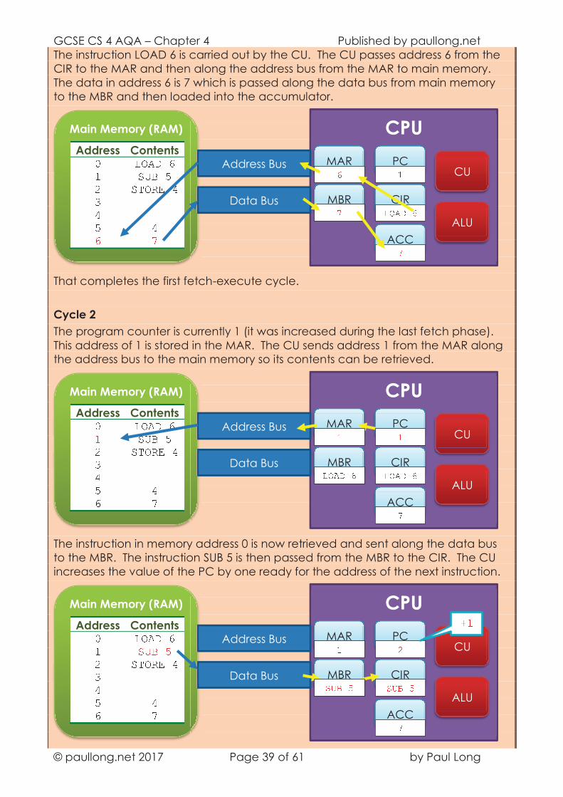
The instruction LOAD 6 is carried out by the CU. The CU passes address 6 from the
CIR to the MAR and then along the address bus from the MAR to main memory.
The data in address 6 is 7 which is passed along the data bus from main memory
to the MBR and then loaded into the accumulator.
That completes the first fetch-execute cycle.
Cycle 2
The program counter is currently 1 (it was increased during the last fetch phase).
This address of 1 is stored in the MAR. The CU sends address 1 from the MAR along
the address bus to the main memory so its contents can be retrieved.
The instruction in memory address 0 is now retrieved and sent along the data bus
to the MBR. The instruction SUB 5 is then passed from the MBR to the CIR. The CU
increases the value of the PC by one ready for the address of the next instruction.
CPU
MAR PC
MBR CIR
ACC
ALU
CU
Main Memory (RAM)
Address Contents H I J K L MN O P Q RS O T J U V WcWR WM Y
Address Bus
Data Bus d _ [ \ ] ^ _`d
CPU
MAR PC
MBR CIR
ACC
ALU
CU
Main Memory (RAM)
Address Contents H I J K L MN O P Q RS O T J U V WXWR WM Y
Address Bus
Data Bus [ \ ] ^ _` [ \ ] ^ _`d
CPU
MAR PC
MBR CIR
ACC
ALU
CU
Main Memory (RAM)
Address Contents e f g h i jN O P Q RS O T J U V WXWR WM Y
Address Bus
Data Bus k l m n` k l m nod
p N

GCSE CS 4 AQA – Chapter 4 Published by paullong.net
© paullong.net 2017 Page 40 of 61 by Paul Long
The instruction in the CIR is decoded by the CU. SUB is recognised as the
instruction (op-code) and 5 is recognised as the address (operand). The CU
passes memory address 5 from the CIR to the MAR and then along the address bus
to main memory. The data value of 4 in memory address 5 is now retrieved and
sent along the data bus to the MBR. The ALU subtracts 4 from the accumulator.
The accumulator’s value is now 3 (7 – 4).
That completes the second fetch-execute cycle.
Cycle 3
The program counter is currently 2. This address of 2 is stored in the MAR. The CU
sends address 2 from the MAR along the address bus to the main memory so its
contents can be retrieved.
CPU
MAR PC
MBR CIR
ACC
ALU
CU
Main Memory (RAM)
Address Contents H I J K L Mq r s t uS O T J U V WXWR WM Y
Address Bus
Data Bus v n k l m now x W
CPU
MAR PC
MBR CIR
ACC
ALU
CU
Main Memory (RAM)
Address Contents H I J K L MN O P Q RS O T J U V WcWR WM Y
Address Bus
Data Bus [ \ ] ^ _o [ \ ] ^ _ow

GCSE CS 4 AQA – Chapter 4 Published by paullong.net
© paullong.net 2017 Page 41 of 61 by Paul Long
The instruction in memory address 2 is now retrieved and sent along the data bus
to the MBR. The instruction STORE 4 is then passed from the MBR to the CIR. The CU
increases the value of the PC by one ready for the address of the next instruction.
The instruction in the CIR is decoded by the CU. STORE is recognised as the
instruction (op-code) and 4 is recognised as the address (operand).
The instruction STORE 4 is carried out by the CU. Address 4 is passed from the CIR
to the MAR. The CU sends the address 4 along the address bus from the MAR to
main memory. The data in the accumulator is 3 which is passed to the MBR and
then along the data bus from the MBR and stored into memory location 4. The
data in memory location 4 is now the value 3.
This completes the final fetch-execute cycle. 7 - 4 = 3.
1) Follow through the animation of the fetch-execute cycle at
http://www.hartismere.com/staticvle/ictskills/FetchExecute.swf - watch how
the values in the registers change and how data is retrieved from memory
and stored to memory.
CPU
MAR PC
MBR CIR
ACC
ALU
CU
Main Memory (RAM)
Address Contents H I J K L MN O P Q RS O T J U V WcWR WM Y
Address Bus
Data Bus k y \ z { vo k y \ z { vww
CPU
MAR PC
MBR CIR
ACC
ALU
CU
Main Memory (RAM)
Address Contents H I J K L MN O P Q R| r } g ~ � �XW XR WM Y
Address Bus
Data Bus w v k y \ z { vow
p N

GCSE CS 4 AQA – Chapter 4 Published by paullong.net
© paullong.net 2017 Page 42 of 61 by Paul Long
2) The contents of main memory and the CPU registers are currently:
a) What is the data in memory address 4?
b) What is the instruction in memory address 2?
c) What is the purpose of the instructions above?
d) What will the value of memory address 6 be when the instructions
have completed?
e) What will the value of the MAR be during the fetch phase of the first
fetch-execute cycle?
f) What will the value of the MBR be at the end of the fetch phase of the
first fetch-execute cycle?
g) What will the value of the accumulator (ACC) be at the end of the
first fetch-execute cycle?
h) At the end of the second fetch-execute cycle, the values in memory
and the registers will be:
i) What will the value of MBR be at the end of the final fetch-
execute cycle?
ii) What will the value of PC be at the end of the final fetch-execute
cycle?
iii) Explain what happens to the contents of memory and the
address bus during the final fetch-execute cycle.
CPU
MAR PC
MBR CIR
ACC
ALU
CU
Main Memory (RAM)
Address Contents H 7 8 9 : EN 9 : : @S = B 8 C D ;XW FR �M
Address Bus
Data Bus
Z
CPU
MAR PC
MBR CIR
ACC
ALU
CU
Main Memory (RAM)
Address Contents H 7 8 9 : EN 9 : : @S = B 8 C D ;XW FR �M
Address Bus
Data Bus � ` ] ^ ^ no` `