c3 - pll - 2 file2 c3-pll-2 overview 6 3 c3-pll-2 pinout 7 4 pll operation 8 5 pll configuration 12...
TRANSCRIPT
CologneChip
C3 - PLL - 2
Phase-locked Loop (PLL)
Frequency Synthesizer IP Core
Implemented in DIGICCTM Technology
Data Sheet � June 2005
C3-PLL-2CologneChip
Cologne Chip AGEintrachtstrasse 113D - 50668 KölnGermany
Tel.: +49 (0) 221 / 91 24-0Fax: +49 (0) 221 / 91 24-100
http://www.C3ip.comhttp://[email protected]
Copyright 1994 - 2005 Cologne Chip AGAll Rights Reserved
The information presented can not be considered as assured characteristics. Data can change without notice.Parts of the information presented may be protected by patent or other rights.
Cologne Chip products are not designed, intended, or authorized for use in any applicationintended to support or sustain life, or for any other application in which the failure of theCologne Chip product could create a situation where personal injury or death may occur.
2 of 20 Data Sheet June 2005
C3-PLL-2CologneChip
Contents
1 DIGICCTM technology 5
2 C3-PLL-2 overview 6
3 C3-PLL-2 pinout 7
4 PLL operation 8
5 PLL configuration 12
5.1 Overview . . . . . . . . . . . . . . . . . . . . . . . . . . . . . . . . . . . . . . . . 12
5.2 Step 1: Determination of the entire solution space for the oscillator-to-output relation 12
5.3 Step 2: Determination of the entire solution space for the input-to-output relation . . 13
5.4 Step 3: Approximation quality (approximation only) . . . . . . . . . . . . . . . . . 14
5.5 Step 4: Calculation of all existing solutions or a set of good solutions . . . . . . . . . 15
5.6 Step 5: Selection of the best PLL configuration setting . . . . . . . . . . . . . . . . 16
5.7 PLL configuration settings for exemplary input / output frequencies . . . . . . . . . . 16
6 Electrical Performance 19
7 Deliverables 19
References 19
June 2005 Data Sheet 3 of 20
C3-PLL-2CologneChip
4 of 20 Data Sheet June 2005
C3-PLL-2CologneChip
1 DIGICCTM technology
Background
Being successful in ASIC design for over ten years, the experience of Cologne Chip’s R&D teamin digital engineering has led to an in-depth know-how especially in the field of telecommunicationinterfaces. Millions of sold microchips underline the company’s expertise in ASIC and FPGA design.This core competence of Cologne Chip becomes now IP core competence: Cologne Chip introducesseveral ASIC IPs to the market under the brand name C3IP.
Design approach
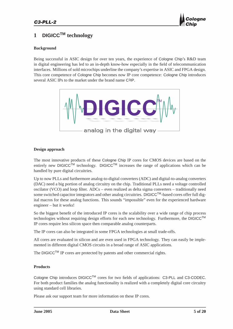
The most innovative products of these Cologne Chip IP cores for CMOS devices are based on theentirely new DIGICCTM technology. DIGICCTM increases the range of applications which can behandled by pure digital circuitries.
Up to now PLLs and furthermore analog-to-digital converters (ADC) and digital-to-analog converters(DAC) need a big portion of analog circuitry on the chip. Traditional PLLs need a voltage controlledoscilator (VCO) and loop filter. ADCs – even realized as delta sigma converters – traditionally needsome switched capacitor integrators and other analog circuitries. DIGICCTM-based cores offer full dig-ital macros for these analog functions. This sounds “impossible” even for the experienced hardwareengineer – but it works!
So the biggest benefit of the introduced IP cores is the scalability over a wide range of chip processtechnologies without requiring design efforts for each new technology. Furthermore, the DIGICCTM
IP cores require less silicon space then comparable analog counterparts.
The IP cores can also be integrated in some FPGA technologies at small trade-offs.
All cores are evaluated in silicon and are even used in FPGA technology. They can easily be imple-mented in different digital CMOS circuits in a broad range of ASIC applications.
The DIGICCTM IP cores are protected by patents and other commercial rights.
Products
Cologne Chip introduces DIGICCTM cores for two fields of applications: C3-PLL and C3-CODEC.For both product families the analog functionality is realized with a completely digital core circuitryusing standard cell libraries.
Please ask our support team for more information on these IP cores.
June 2005 Data Sheet 5 of 20
C3-PLL-2CologneChip
2 C3-PLL-2 overview
Until today hardware engineers have to rely on analog VCOs for general purpose phase-locked loops(PLL). Cologne Chip has come up now with a fully digital approach: The C3-PLL-2 core for a broadrange of frequency synthesizer applications.
This document describes the PLL IP core C3-PLL-2 including feature list, pinout, block diagram,operational characteristics and electrical parameters.
The C3-PLL-2 is based on the DIGICCTM technology of CologneChip, which makes it possible to be easily implemented in all kindsof digital CMOS circuits as a fully digital circuit using standard celllibraries. The used circuit area is smaller than that of competing
technologies. Furthermore the lock time is very short and it is even super-fast when the PLL isrestarted after standby mode.
Because of its pure digital nature, the C3-PLL-2 does neither require any additional PAD or pin norexternal or internal loop capacitors. External filters for the supply voltage are normally not needed.A patent is pending for this new Cologne Chip technology.
The C3-PLL-2 is based on the C3-PLL-1 IP core [2] and contains additional read / write registers withaddress decoder, a predivider and a post-scaler.
Technical Features
• Fully digital, designed for use with standard cell libraries for digital logic
• Implementable in any digital CMOS process technology
• Typical oscillator frequency ranges: 0.50 µm: fosc = 60 . .120MHz
0.35 µm: fosc = 100 . .200MHz
0.25 µm: fosc = 140 . .280MHz
0.18 µm: fosc = 160 . .320MHz
0.13 µm: fosc = 180 . .360MHz
90 nm: fosc = 200 . .400MHz
• Frequency multiplication range 5 . .255
• Predivider and post-scaler with divider range 1 . . 256 each
• Jitter similar to analogue PLLs
• No additional pins or PADs
• No external loop filter or filter capacity needed
• Supply voltage filter is not required
• Very short lock time (worst case 2000 reference clocks)
• Standby mode to stop oscillator but preserve center frequency→ super-fast slock time when returning from standby mode (only some clock cycles)
• Standby mode also reduces power consumption to zero (only leakage current)
• Very small silicon area (< 3000 gates)
6 of 20 Data Sheet June 2005
C3-PLL-2CologneChip
Application fields
C3-PLL-2 has some outstanding benefits which makes the IP core interesting for several applicationfields.
• C3-PLL-2 is a clock generator device for CPUs, MCUs and peripheral devices, e.g. USB chips.
• Due to the fully digital approach, C3-PLL-2 can be used in FPGA applications.
• The very short lock time is useful in many applications where the start-up time must be verysmall (e.g. RF devices), especially for low power applications.
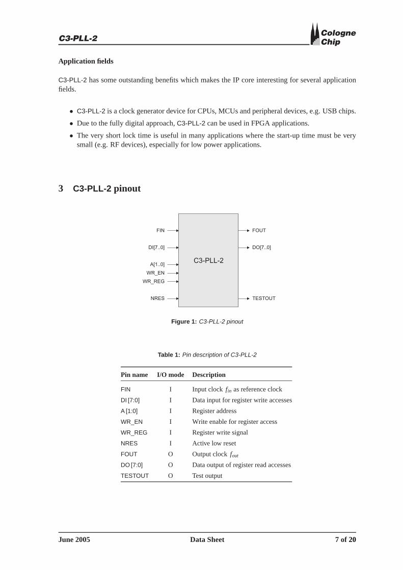
3 C3-PLL-2 pinout
DI[7..0]
FIN
C3-PLL-2
FOUT
A[1..0]
WR_EN
WR_REG
DO[7..0]
TESTOUTNRES
Figure 1: C3-PLL-2 pinout
Table 1: Pin description of C3-PLL-2
Pin name I/O mode Description
FIN I Input clock fin as reference clock
DI [7:0] I Data input for register write accesses
A [1:0] I Register address
WR_EN I Write enable for register access
WR_REG I Register write signal
NRES I Active low reset
FOUT O Output clock fout
DO [7:0] O Data output of register read accesses
TESTOUT O Test output
June 2005 Data Sheet 7 of 20
C3-PLL-2CologneChip
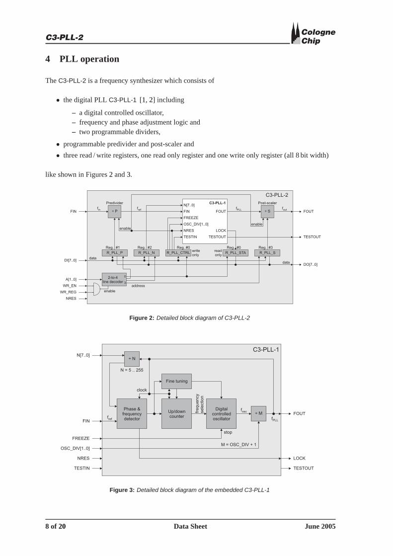
4 PLL operation
The C3-PLL-2 is a frequency synthesizer which consists of
• the digital PLL C3-PLL-1 [1, 2] including
– a digital controlled oscillator,– frequency and phase adjustment logic and– two programmable dividers,
• programmable predivider and post-scaler and
• three read / write registers, one read only register and one write only register (all 8 bit width)
like shown in Figures 2 and 3.
2-to-4line decoder
0
3
R_PLL_STA
N[7..0]
FIN
C3-PLL-1
FOUT
FREEZE
NRES
TESTIN
LOCK
TESTOUT
OSC_DIV[1..0]
R_PLL_P R_PLL_N R_PLL_SR_PLL_CTRL
Post-scaler
÷ S
Predivider
÷ P
C3-PLL-2
A[1..0]
WR_EN
WR_REG
DI[7..0]DO[7..0]
Reg. #1 Reg. #2 Reg. #3
FIN
Reg. #0
FOUT
TESTOUT
data
address
data
readonly
Reg. #0writeonly
NRES
fPLLfref foutfin
enable
enableenable
Figure 2: Detailed block diagram of C3-PLL-2
÷ M
÷ NN[7..0]
FIN
C3-PLL-1
FOUT
FREEZE
NRES
TESTIN
Up/downcounter
Fine tuning
Phase &frequencydetector
LOCK
TESTOUT
Digitalcontrolledoscillator
stop
OSC_DIV[1..0]
frequency
sele
ction
fosc
M = OSC_DIV + 1
fref fPLL
clock
N = 5 .. 255
Figure 3: Detailed block diagram of the embedded C3-PLL-1
8 of 20 Data Sheet June 2005
C3-PLL-2CologneChip
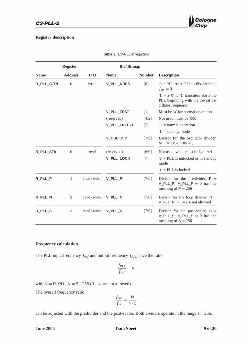
Register description
Table 2: C3-PLL-2 registers
Register Bit / Bitmap
Name Address I / O Name Number Description
R_PLL_CTRL 0 write V_PLL_NRES [0] ’0’ = PLL reset, PLL is disabled andfout = 0
’1’ = a ’0’ to ’1’ transition starts thePLL beginning with the lowest os-cillator frequency
V_PLL_TEST [1] Must be ’0’ for normal operation
(reserved) [4:2] Not used, must be ’000’
V_PLL_FREEZE [5] ’0’ = normal operation
’1’ = standby mode
V_OSC_DIV [7:6] Divisor for the oscillator divider,M = V_OSC_DIV+1
R_PLL_STA 0 read (reserved) [6:0] Not used, value must be ignored
V_PLL_LOCK [7] ’0’ = PLL is unlocked or in standbymode
’1’ = PLL is locked
R_PLL_P 1 read / write V_PLL_P [7:0] Divisor for the predivider, P =V_PLL_P, V_PLL_P = 0 has themeaning of P = 256
R_PLL_N 2 read / write V_PLL_N [7:0] Divisor for the loop divider, N =V_PLL_N, 0 . . 4 are not allowed
R_PLL_S 3 read / write V_PLL_S [7:0] Divisor for the post-scaler, S =V_PLL_S, V_PLL_S = 0 has themeaning of S = 256
Frequency calculation
The PLL input frequency fre f and output frequency fPLL have the ratio
fPLL
fre f= N
with N = R_PLL_N = 5 . .255 (0 . . 4 are not allowed).
The overall frequency ratiofout
fin=
N
P ·S
can be adjusted with the predivider and the post-scaler. Both dividers operate in the range 1 . . 256.
June 2005 Data Sheet 9 of 20
C3-PLL-2CologneChip
An additional divider is implemented between the oscillator and the loop feedback. The oscillatorcovers a frequency range of
fOSC,max
fOSC,min> 2 .
The actual limiting values depend on the CMOS process technology (listed on page 6) and the delayparameter of the digital library used.
The oscillator divider can be used to generate a lower output frequency
fPLL =fOSC
M
where M = V_OSC_DIV+1 = 1 . .4.
Furthermore, the power consumption of the C3-PLL-2 core is decreased the larger M is chosen. Thisis due to the fact that main parts of the PLL are clocked by the fPLL pulses.
Register write access
Register values are written with WR_EN = WR_REG = ’1’ after data input DI[7:0] and address A[1:0]are valid. Hold and setup time is 2 ns.
All registers are set to 0x00 during reset state NRES = ’0’.
Register read access
The data port DO[7:0] issues always valid data of the addressed register.
PLL reset
Two different reset procedures are available for C3-PLL-2.
1. A programmable reset with V_PLL_NRES = ’0’ in register R_PLL_CFG
• resets the embedded C3-PLL-1 core,
• switches off the fout generation
• but does not change the programming registers.
The PLL starts always with the lowest possible fosc frequency after V_NRES has been set to ’1’.
2. The reset signal NRES of the C3-PLL-2 core
• resets the complete PLL including the programming registers and the embedded C3-PLL-1core and
• keeps the predivider and the post-scaler in reset state as long as NRES signal is low.
NRES should be low for at least 10 ns. fout is switched off during reset.
10 of 20 Data Sheet June 2005
C3-PLL-2CologneChip
Startup phase
V_PLL_NRES = ’1’ in register R_PLL_CTRL enables the oscillator. The PLL starts always with thelowest possible fosc frequency.
During the startup phase, fosc rises without overshoots until the nominal frequency is reached. Thisprocedure takes 2000 clock cycles of fre f at worst case, so that
tlock ≤ 2000 ·Pfin
.
The PLL uses only the rising edge of fin. Thus neither the duty cycle nor the jitter of the falling edgeinfluence the C3-PLL-2 behavior.
The detector output signal triggers an up / down counter which is used to select the frequency ofthe oscillator. A fine tuning capability is implemented to achieve oscillator frequencies with a highprecision.
A new value for N can be set unsynchronized to the reference frequency fre f .
V_PLL_LOCK = ’1’ in register R_PLL_STA signals that the PLL is locked.
Jitter characteristics
Because of the operation method of the PLL, there is some jitter at the output signal fPLL even if thereference signal fre f has no jitter. Additionally there is some jitter induced by supply voltage noise.So if the jitter is a critical parameter special measures should be taken to reduce power supply jitter.
The overall jitter Jtot isJtot = Jdet + Jpow + k · Jin
where Jdet is the deterministic jitter, Jpow is the jitter caused by the power supply and Jin is the jitter ofthe reference frequency fre f . There is a jitter frequency dependent attenuation factor k < 1 betweenthe input jitter of fre f and the output jitter Jin.
PLL standby mode
The C3-PLL-2 can be switched into standby mode with V_PLL_FREEZE = ’1’ in register R_PLL_CTRL.Then the oscillator is disabled and the whole PLL logic is unclocked. The power consumption is zero,only process dependent leackage current occurs. The center frequency of the PLL is preserved be-cause the entire state of the digital controller is stored.
After V_PLL_FREEZE has been set back to ’0’, a small readjustment might be necessary due to tem-perature drift, supply voltage drift or a slight fin change. This readjustment takes only a few fre f
cycles, typically. So the relock time after standby is significantly shorter than the initial lock time.
The V_PLL_LOCK bit in register R_PLL_STA is ’0’ during standby mode.
June 2005 Data Sheet 11 of 20
C3-PLL-2CologneChip
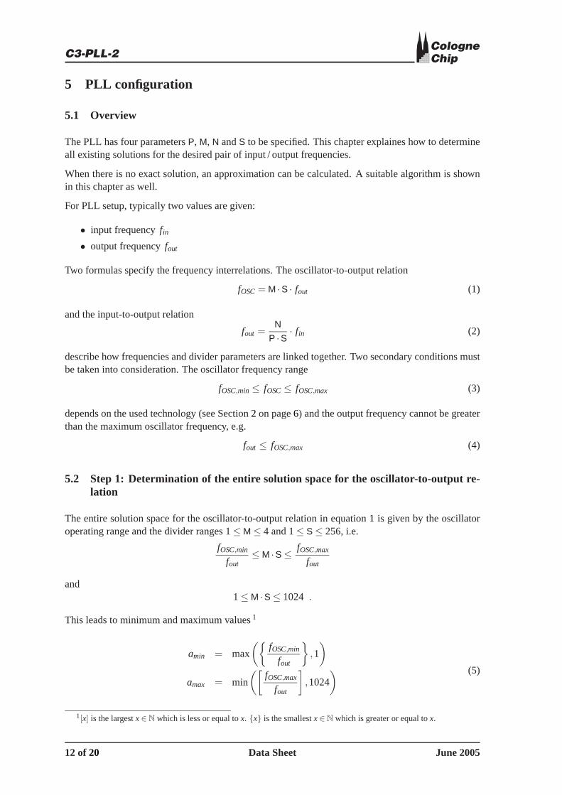
5 PLL configuration
5.1 Overview
The PLL has four parameters P, M, N and S to be specified. This chapter explaines how to determineall existing solutions for the desired pair of input / output frequencies.
When there is no exact solution, an approximation can be calculated. A suitable algorithm is shownin this chapter as well.
For PLL setup, typically two values are given:
• input frequency fin
• output frequency fout
Two formulas specify the frequency interrelations. The oscillator-to-output relation
fOSC = M ·S · fout (1)
and the input-to-output relation
fout =N
P ·S · fin (2)
describe how frequencies and divider parameters are linked together. Two secondary conditions mustbe taken into consideration. The oscillator frequency range
fOSC,min ≤ fOSC ≤ fOSC,max (3)
depends on the used technology (see Section 2 on page 6) and the output frequency cannot be greaterthan the maximum oscillator frequency, e.g.
fout ≤ fOSC,max (4)
5.2 Step 1: Determination of the entire solution space for the oscillator-to-output re-lation
The entire solution space for the oscillator-to-output relation in equation 1 is given by the oscillatoroperating range and the divider ranges 1 ≤ M ≤ 4 and 1 ≤ S ≤ 256, i.e.
fOSC,min
fout≤ M ·S ≤ fOSC,max
fout
and1 ≤ M ·S ≤ 1024 .
This leads to minimum and maximum values 1
amin = max
({fOSC,min
fout
},1
)
amax = min
([fOSC,max
fout
],1024
) (5)
1[x] is the largest x ∈ N which is less or equal to x. {x} is the smallest x ∈ N which is greater or equal to x.
12 of 20 Data Sheet June 2005
C3-PLL-2CologneChip
which cover all possible a = M ·S values 2.
Every a = amin . .amax must be split into tuples for M and S so that
A = {(M,S) | amin ≤ M ·S ≤ amax ∧ M ≤ 4 ∧ S ≤ 256} ⊆ N+×N+ (6)
Set A contains all possible tuples (M,S) and is used in step 4 afterwards.
5.3 Step 2: Determination of the entire solution space for the input-to-output relation
Exact approach
The relation of input and output frequencies
fout
fin=
bc
is reduced so that b,c ∈ N+ are coprime.
When the dividers are set to N = b and P ·S = c, these are the smallest values that can be reached forN, P and S.
� Please note !
There is no exact solution for the given pair of input and output frequencies ifb > 255 or c > 65536. See below how approximations can be determined in thiscase.
Additional solutions exist in many cases. The entire solution space can be determined from this byexpanding
bc
=b ·dc ·d ; d ∈ N+
within the valid ranges. This leads to minimum and maximum values
dmin =
⎧⎪⎪⎨⎪⎪⎩
5 ; b = 1
(5 div b)+1 ; 2 ≤ b ≤ 4
1 ; b ≥ 5
dmax = min(255 div b,65536 div c) .
(7)
The equation results for dmin are shown in Table 3.
Every x = c ·dmin . .c ·dmax must be split into tuples for P and S so that
X = {(P,S) | dmin ≤ P ·Sc
≤ dmax ∧ (P ·S) mod c = 0 ∧P ≤ 256 ∧ S ≤ 256} ⊆ N+×N+ (8)
Set X contains all possible tuples (P,S) and is used in step 4 afterwards.
2Due to equation 4, amax cannot be smaller than amin.
June 2005 Data Sheet 13 of 20
C3-PLL-2CologneChip
Table 3: dmin determination
b : 1 2 3 4 ≥ 5
dmin : 5 3 2 2 1
Approximation
There is no exact solution for the given pair of input and output frequencies when either b or c or evenboth values are too large. Good approximations
fout
fin≈ b′
c′; b′,c′ ∈ N+ (9)
for the output frequency might exist and are determined in the following.
As b′ ∈ N+ is in the range 5 . . 255 and for every tuple (b′,c′) there is one
c′1(b′) =
[finfout
·b′]
; c′1 ∈ N+
which is a little bit too small and one
c′2(b′) = c′1(b
′)+1
which is a little bit too large, there are up to 502 approximations for equation 9. The set
F = F1 ∪F2 (10)
contains only those approximations which have c′ in its valid range. The subsets are defined by
F1 = {(b′,c′) | 5 ≤ b′ ≤ 255 ∧ c′ = c′1(b′) ∧ c′ ≤ 65536} ⊆ N+×N+
F2 = {(b′,c′) | 5 ≤ b′ ≤ 255 ∧ c′ = c′2(b′) ∧ c′ ≤ 65536} ⊆ N+×N+
(11)
and are used in step 4 afterwards.
� Please note !
When F is empty, there is no solution for the given pair of input and outputfrequencies.
5.4 Step 3: Approximation quality (approximation only)
This step has only to be executed for approximations.
All approximation results are based on the set F given in equations 10 and 11. As there are good aswell as very poor approximations to the desired fout frequency, the tuple (b′,c′) which leads to theminimum frequency offset should be selected from F .
14 of 20 Data Sheet June 2005
C3-PLL-2CologneChip
The minimum frequency offset
∆ fout,min(b,c) = min
∣∣∣∣b′
c′· fin − fout
∣∣∣∣ ∀ (b′,c′) ∈ F (12)
has to be found 3. So the actual output frequency is
f ′out =bc· fin .
The tuple (b,c) is the best approximation available in F . But this is not necessarily a solution for thePLL configuration because further criteria must be fulfilled.
c stands for an integer product of P and S. The set
X = {(P,S) | P ·S = c ∧ P ≤ 256 ∧ S ≤ 256} ⊆ N+×N+ (13)
contains all valid tuples (P,S) derived from c.
� Please note !
Step 3 can be varied as follows:
Equation 12 selects only the tuple (b′,c′) with the best approximation. Alterna-tively, the user could specify the minimum required precision of fout . Then alltuples (b′,c′) can be selected that fullfil this requirement. Typically, this leads toa larger number of solutions in step 4, which then might give a better selection instep 5.
5.5 Step 4: Calculation of all existing solutions (exact approach) or a set of good solu-tions (approximation)
Up to here, the partial results for equations 1 and 2 are determined. These results, given in two setsA (eqn. 6) and X (either eqn. 8 or eqn. 13) have been determined independendly from each other.
They are connected due to the fact, that both contain terms of S, namely a = M ·S and x = P ·S.
Only those tuples of A and X can be a solution that have the same value for S. These fill up the set
C = {(P,M,N,S) | (P,S) ∈ X ∧ (M,S) ∈ A ∧N =
f ′out
fin·P ·S ∧ 5 ≤ N ≤ 255} ⊆ N+×N+×N+×N+ (14)
which contains all exisiting solutions for the given pair of input and output frequencies that can exactlybe reached or that fullfil equation 12.
3|x| is the absolute value of x.
June 2005 Data Sheet 15 of 20

C3-PLL-2CologneChip
Exact approach
When C is empty, there is no exact solution for the given pair of input and output frequencies. Anapproximation can be calculated using equation 9 where all tuples (b′,c′) are eliminated that fullfilb′ ∈ b ·dmin . .b ·dmax and c′ ∈ c ·dmin . .c ·dmax (refer to equations 7 and 8).
Approximation
When C is empty, the selected tuple (b,c)∈ F cannot be used for the PLL configuration setting. Thistuple should be eliminated from F , i.e.
F −→ F \ (b,c)
and steps 3 and 4 have to be executed again. This loop selects always the best available approximationbut the approximation quality decreases with every loop iteration.
The procedure ends when either C �= {} or F = {}.
It is unlikely that F = {} happens. This would mean that there is neither an exact nor an approximatesolution even though the chosen pair of input and output frequencies are in a valid range.
5.6 Step 5: Selection of the best PLL configuration setting
Finally, the best PLL configuration setting can be selected from the solution set C . It is assumed thatC is not empty.
The phase & frequency detector of the PLL should receive a high reference frequency to execute thedetection procedure in small time intervals. This leads to the first selection rule:
1. selection rule: P should be as small as possible.
If several solutions of C match the first rule, it is recommended to minimize the power consumption.This is equal to a large M value:
2. selection rule: M should be as large as possible.
These two rules fix the other divider values N and S. So there is no further selection rule.
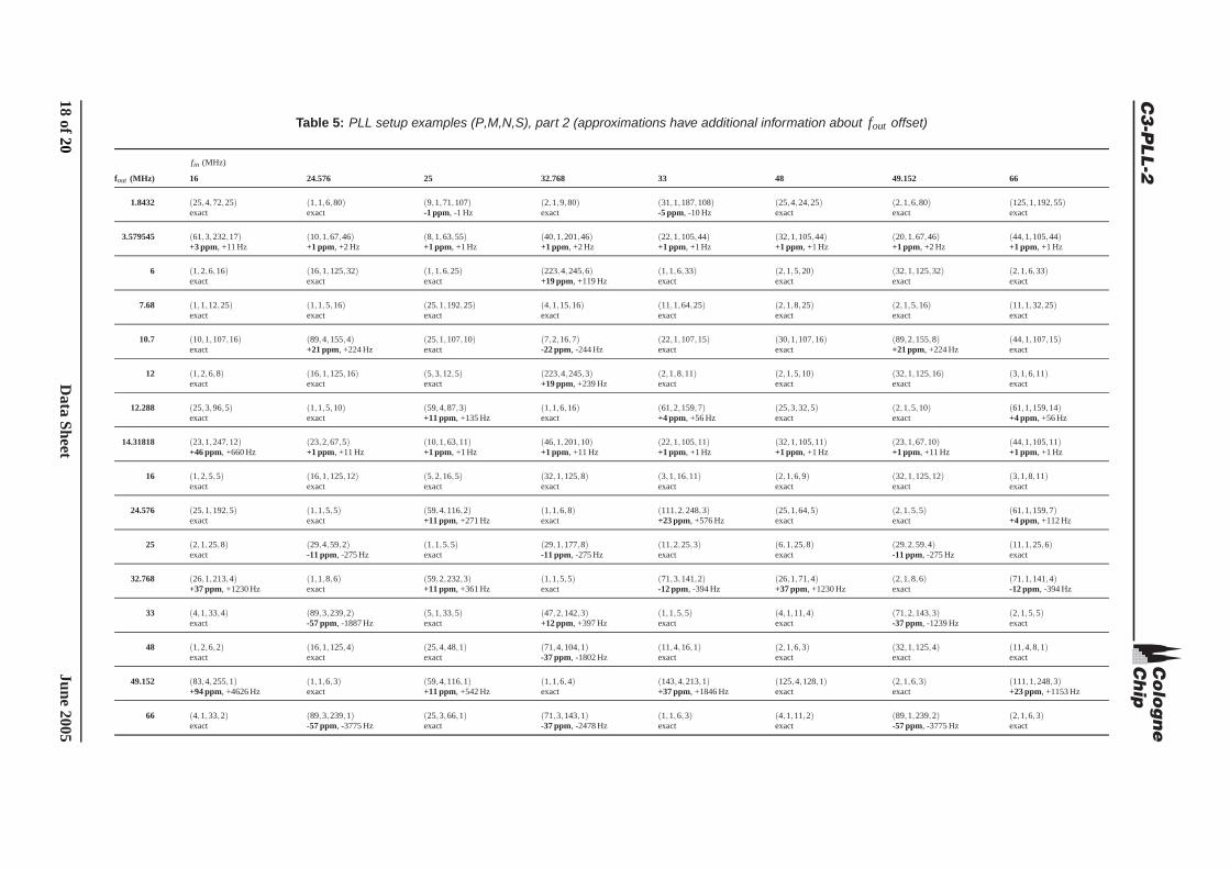
5.7 PLL configuration settings for exemplary input / output frequencies
Table 4 and 5 show examples for PLL configuration settings. The parameter tuple (P,M,N,S) is givenfor often used frequencies 4. Approximate solutions have additional information about the fout offsetin parts per million and absolute value.
4A PERL script for the determination of PLL configuration settings is avaliable on request [email protected].
16 of 20 Data Sheet June 2005

C3
-PL
L-2
Co
log
ne
Ch
ip
Table 4: PLL setup examples (P,M,N,S), part 1 (approximations have additional information about fout offset)
fin (MHz)
fout (MHz) 1.8432 3.579545 6 7.68 10.7 12 12.288 14.31818
1.8432 (1,4,14,14)exact
(2,1,69,67)-1 ppm, -1 Hz
(25,4,192,25)exact
(1,4,6,25)exact
(13,1,159,71)+15 ppm, +28 Hz
(25,4,96,25)exact
(1,2,6,40)exact
(8,1,69,67)-1 ppm, -1 Hz
3.579545 (3,2,134,23)+1 ppm, +2 Hz
(1,4,7,7)exact
(4,1,105,44)+1 ppm, +1 Hz
(59,4,220,8)+32 ppm, +116 Hz
(79,4,185,7)+5 ppm, +21 Hz
(8,1,105,44)+1 ppm, +1 Hz
(5,1,67,46)+1 ppm, +2 Hz
(1,2,5,20)exact
6 (3,1,166,17)-94 ppm, -564 Hz
(5,1,176,21)+1 ppm, +1 Hz
(1,4,5,5)exact
(1,1,25,32)exact
(1,3,5,10)exact
(8,1,125,32)exact
(5,1,44,21)+1 ppm, +1 Hz
7.68 (1,4,25,6)exact
(5,2,118,11)-32 ppm, -248 Hz
(1,1,32,25)exact
(1,4,5,5)exact
(41,3,206,7)+18 ppm, +139 Hz
(1,1,16,25)exact
(1,3,5,8)exact
(53,3,199,7)+13 ppm, +101 Hz
10.7 (2,1,209,18)+74 ppm, +800 Hz
(5,1,254,17)-324 ppm, -3477 Hz
(4,1,107,15)exact
(9,1,163,13)-47 ppm, -512 Hz
(1,3,5,5)exact
(8,1,107,15)exact
(21,2,128,7)-22 ppm, -244 Hz
(31,3,139,6)+13 ppm, +145 Hz
12 (3,1,254,13)+369 ppm, +4430 Hz
(6,1,181,9)-157 ppm, -1895 Hz
(1,4,6,3)exact
(1,1,25,16)exact
(1,3,5,5)exact
(8,1,125,16)exact
(7,1,88,15)-1 ppm, -1 Hz
12.288 (1,4,20,3)exact
(2,1,103,15)+144 ppm, +1771 Hz
(8,1,213,13)+37 ppm, +461 Hz
(1,3,8,5)exact
(31,3,178,5)-21 ppm, -258 Hz
(25,3,128,5)exact
(1,3,5,5)exact
(67,4,230,4)-1 ppm, -9 Hz
14.31818 (1,1,101,13)+144 ppm, +2066 Hz
(1,4,8,2)exact
(4,1,105,11)+1 ppm, +1 Hz
(59,4,220,2)+32 ppm, +464 Hz
(17,3,91,4)+65 ppm, +937 Hz
(8,1,105,11)+1 ppm, +1 Hz
(23,2,134,5)+1 ppm, +11 Hz
(1,2,5,5)exact
16 (5,2,217,5)-64 ppm, -1024 Hz
(7,1,219,7)-101 ppm, -1625 Hz
(1,4,8,3)exact
(1,1,25,12)exact
(1,2,8,6)exact
(8,1,125,12)exact
(71,4,238,3)-80 ppm, -1282 Hz
24.576 (1,2,40,3)exact
(3,1,103,5)+144 ppm, +3542 Hz
(13,2,213,4)+37 ppm, +923 Hz
(1,1,16,5)exact
(8,1,147,8)+22 ppm, +562 Hz
(13,1,213,8)+37 ppm, +923 Hz
(1,2,6,3)exact
(67,4,230,2)-1 ppm, -19 Hz
25 (2,1,217,8)-64 ppm, -1600 Hz
(6,1,251,6)-1704 ppm, -42616 Hz
(1,1,25,6)exact
(47,4,153,1)+34 ppm, +851 Hz
(107,4,250,1)exact
(2,1,25,6)exact
(29,4,59,1)-11 ppm, -275 Hz
(9,1,110,7)-1 ppm, -3 Hz
32.768 (3,2,160,3)exact
(13,4,119,1)-42 ppm, -1395 Hz
(13,4,71,1)+37 ppm, +1230 Hz
(3,1,64,5)exact
(4,1,49,4)+22 ppm, +750 Hz
(13,3,71,2)+37 ppm, +1230 Hz
(1,2,8,3)exact
(13,1,119,4)-42 ppm, -1395 Hz
33 (2,1,179,5)-203 ppm, -6720 Hz
(23,4,212,1)-179 ppm, -5933 Hz
(1,3,11,2)exact
(37,4,159,1)+98 ppm, +3243 Hz
(71,4,219,1)+128 ppm, +4225 Hz
(1,1,11,4)exact
(89,4,239,1)-57 ppm, -1887 Hz
(21,1,242,5)-1 ppm, -4 Hz
48 (1,4,26,1)-1600 ppm, -76800 Hz
(17,4,228,1)+166 ppm, +8015 Hz
(1,4,8,1)exact
(1,1,25,4)exact
(35,4,157,1)-59 ppm, -2857 Hz
(1,2,8,2)exact
(8,1,125,4)exact
(71,4,238,1)-80 ppm, -3847 Hz
49.152 (1,1,80,3)exact
(5,1,206,3)+144 ppm, +7084 Hz
(13,2,213,2)+37 ppm, +1846 Hz
(5,4,32,1)exact
(8,1,147,4)+22 ppm, +1125 Hz
(13,1,213,4)+37 ppm, +1846 Hz
(1,2,8,2)exact
(67,4,230,1)-1 ppm, -38 Hz
66 (5,3,179,1)-203 ppm, -13440 Hz
(3,1,166,3)+344 ppm, +22718 Hz
(1,3,11,1)exact
(9,1,232,3)-134 ppm, -8888 Hz
(2,1,37,3)-252 ppm, -16666 Hz
(1,1,11,2)exact
(35,3,188,1)+62 ppm, +4114 Hz
(41,3,189,1)+50 ppm, +3317 Hz
June2005
Data
Sheet17
of20
C3
-PL
L-2
Co
log
ne
Ch
ip
Table 5: PLL setup examples (P,M,N,S), part 2 (approximations have additional information about fout offset)
fin (MHz)
fout (MHz) 16 24.576 25 32.768 33 48 49.152 66
1.8432 (25,4,72,25)exact
(1,1,6,80)exact
(9,1,71,107)-1 ppm, -1 Hz
(2,1,9,80)exact
(31,1,187,108)-5 ppm, -10 Hz
(25,4,24,25)exact
(2,1,6,80)exact
(125,1,192,55)exact
3.579545 (61,3,232,17)+3 ppm, +11 Hz
(10,1,67,46)+1 ppm, +2 Hz
(8,1,63,55)+1 ppm, +1 Hz
(40,1,201,46)+1 ppm, +2 Hz
(22,1,105,44)+1 ppm, +1 Hz
(32,1,105,44)+1 ppm, +1 Hz
(20,1,67,46)+1 ppm, +2 Hz
(44,1,105,44)+1 ppm, +1 Hz
6 (1,2,6,16)exact
(16,1,125,32)exact
(1,1,6,25)exact
(223,4,245,6)+19 ppm, +119 Hz
(1,1,6,33)exact
(2,1,5,20)exact
(32,1,125,32)exact
(2,1,6,33)exact
7.68 (1,1,12,25)exact
(1,1,5,16)exact
(25,1,192,25)exact
(4,1,15,16)exact
(11,1,64,25)exact
(2,1,8,25)exact
(2,1,5,16)exact
(11,1,32,25)exact
10.7 (10,1,107,16)exact
(89,4,155,4)+21 ppm, +224 Hz
(25,1,107,10)exact
(7,2,16,7)-22 ppm, -244 Hz
(22,1,107,15)exact
(30,1,107,16)exact
(89,2,155,8)+21 ppm, +224 Hz
(44,1,107,15)exact
12 (1,2,6,8)exact
(16,1,125,16)exact
(5,3,12,5)exact
(223,4,245,3)+19 ppm, +239 Hz
(2,1,8,11)exact
(2,1,5,10)exact
(32,1,125,16)exact
(3,1,6,11)exact
12.288 (25,3,96,5)exact
(1,1,5,10)exact
(59,4,87,3)+11 ppm, +135 Hz
(1,1,6,16)exact
(61,2,159,7)+4 ppm, +56 Hz
(25,3,32,5)exact
(2,1,5,10)exact
(61,1,159,14)+4 ppm, +56 Hz
14.31818 (23,1,247,12)+46 ppm, +660 Hz
(23,2,67,5)+1 ppm, +11 Hz
(10,1,63,11)+1 ppm, +1 Hz
(46,1,201,10)+1 ppm, +11 Hz
(22,1,105,11)+1 ppm, +1 Hz
(32,1,105,11)+1 ppm, +1 Hz
(23,1,67,10)+1 ppm, +11 Hz
(44,1,105,11)+1 ppm, +1 Hz
16 (1,2,5,5)exact
(16,1,125,12)exact
(5,2,16,5)exact
(32,1,125,8)exact
(3,1,16,11)exact
(2,1,6,9)exact
(32,1,125,12)exact
(3,1,8,11)exact
24.576 (25,1,192,5)exact
(1,1,5,5)exact
(59,4,116,2)+11 ppm, +271 Hz
(1,1,6,8)exact
(111,2,248,3)+23 ppm, +576 Hz
(25,1,64,5)exact
(2,1,5,5)exact
(61,1,159,7)+4 ppm, +112 Hz
25 (2,1,25,8)exact
(29,4,59,2)-11 ppm, -275 Hz
(1,1,5,5)exact
(29,1,177,8)-11 ppm, -275 Hz
(11,2,25,3)exact
(6,1,25,8)exact
(29,2,59,4)-11 ppm, -275 Hz
(11,1,25,6)exact
32.768 (26,1,213,4)+37 ppm, +1230 Hz
(1,1,8,6)exact
(59,2,232,3)+11 ppm, +361 Hz
(1,1,5,5)exact
(71,3,141,2)-12 ppm, -394 Hz
(26,1,71,4)+37 ppm, +1230 Hz
(2,1,8,6)exact
(71,1,141,4)-12 ppm, -394 Hz
33 (4,1,33,4)exact
(89,3,239,2)-57 ppm, -1887 Hz
(5,1,33,5)exact
(47,2,142,3)+12 ppm, +397 Hz
(1,1,5,5)exact
(4,1,11,4)exact
(71,2,143,3)-37 ppm, -1239 Hz
(2,1,5,5)exact
48 (1,2,6,2)exact
(16,1,125,4)exact
(25,4,48,1)exact
(71,4,104,1)-37 ppm, -1802 Hz
(11,4,16,1)exact
(2,1,6,3)exact
(32,1,125,4)exact
(11,4,8,1)exact
49.152 (83,4,255,1)+94 ppm, +4626 Hz
(1,1,6,3)exact
(59,4,116,1)+11 ppm, +542 Hz
(1,1,6,4)exact
(143,4,213,1)+37 ppm, +1846 Hz
(125,4,128,1)exact
(2,1,6,3)exact
(111,1,248,3)+23 ppm, +1153 Hz
66 (4,1,33,2)exact
(89,3,239,1)-57 ppm, -3775 Hz
(25,3,66,1)exact
(71,3,143,1)-37 ppm, -2478 Hz
(1,1,6,3)exact
(4,1,11,2)exact
(89,1,239,2)-57 ppm, -3775 Hz
(2,1,6,3)exact
18of
20D
ataSheet
June2005

C3-PLL-2CologneChip
6 Electrical Performance
The electrical parameters given in Table 6 are valid over the full process range with respect to allprocess technologies listed on page 6, over the full temperature range 0 . . 70 ◦C and over the fullvoltage range VDD ±10%.
Table 6: Electrical performance (over the full process, temperature and voltage range)
Parameter Symbol min. typ. max. Unit
Oscillator Frequency fosc 100 200 MHz
Multiplication Factor N 5 255
Deterministic Jitter *1 120 250 ps
Jitter from Supply Voltage Noise *2 1 2.6 ps/mV
Duty cycle of FOUT 40 60 %
NRES low time 10 ns
Power consumption
in operation *3 mW
standby *4 0 10 100 µW
*1: Clock-to-clock*2: Clock-to-clock, peak-to-peak noise voltage*3: Depends on process technology and output frequency*4: Depends on leackage current of the actual process technology
7 Deliverables
Cologne Chip IP cores consist of a simulated netlist for the destination technology, test vectors for adigital tester environment and behavioral models for evaluation purposes. It can be obtained directlyfrom Cologne Chip. Please contact our Support Team at [email protected].
The business model for C3IP depends on the specific customer case. It could be for example a generallicence for a semiconductor company, a one time licence for an ASIC project or a royalty based modelfor design houses.
References
[1] Cologne Chip AG. DIGICCTM PLL Technology, November 2004.
[2] Cologne Chip AG. C3-PLL-1– Phase-locked Loop (PLL) Frequency Multiplier IP Core, May2005.
June 2005 Data Sheet 19 of 20
Cologne Chip AG
Data Sheet of C3-PLL-2
CologneChip