c: 9 l91 m l91tm.qxd (page 1) - a · pdf filetechnical training fl9.1 lcd tv chassis for 2009...
TRANSCRIPT

TECHNICAL TRAINING
FL9.1 LCD TVCHASSIS FOR2009
P & F USA, INCSUITE 1003015 WINDWARD PLAZAALPHARETTA, GA 30005
Table of contents
Introduction . . . . . . . . . . . . . . . . . . . . . . . . . . . . . . . . . . . . . . . . . . . . . . . . . . . . . . .1Models covered . . . . . . . . . . . . . . . . . . . . . . . . . . . . . . . . . . . . . . . . . . . . . . . . . . . .1Formats Supported . . . . . . . . . . . . . . . . . . . . . . . . . . . . . . . . . . . . . . . . . . . . . . . . .1Menus . . . . . . . . . . . . . . . . . . . . . . . . . . . . . . . . . . . . . . . . . . . . . . . . . . . . . . . . . . .2Software Upgrade . . . . . . . . . . . . . . . . . . . . . . . . . . . . . . . . . . . . . . . . . . . . . . . . . .3Customer Menu Map . . . . . . . . . . . . . . . . . . . . . . . . . . . . . . . . . . . . . . . . . . . . . . . .4Board Locations . . . . . . . . . . . . . . . . . . . . . . . . . . . . . . . . . . . . . . . . . . . . . . . . . . .5Board Level Repair . . . . . . . . . . . . . . . . . . . . . . . . . . . . . . . . . . . . . . . . . . . . . . . . .6Wiring Interconnect Diagram . . . . . . . . . . . . . . . . . . . . . . . . . . . . . . . . . . . . . . . . . .8Video Signal Flow . . . . . . . . . . . . . . . . . . . . . . . . . . . . . . . . . . . . . . . . . . . . . . . . . .9Video Signal Flow Block . . . . . . . . . . . . . . . . . . . . . . . . . . . . . . . . . . . . . . . . . . . . .10Video Signal Flow Block two . . . . . . . . . . . . . . . . . . . . . . . . . . . . . . . . . . . . . . . . . .11Audio Signal Flow . . . . . . . . . . . . . . . . . . . . . . . . . . . . . . . . . . . . . . . . . . . . . . . . . .12Audio Signal Flow Block . . . . . . . . . . . . . . . . . . . . . . . . . . . . . . . . . . . . . . . . . . . . .13Power Supply Block . . . . . . . . . . . . . . . . . . . . . . . . . . . . . . . . . . . . . . . . . . . . . . . .14Power Supply . . . . . . . . . . . . . . . . . . . . . . . . . . . . . . . . . . . . . . . . . . . . . . . . . . . . .15Protect 1 . . . . . . . . . . . . . . . . . . . . . . . . . . . . . . . . . . . . . . . . . . . . . . . . . . . . . . . . .15Protect 2 . . . . . . . . . . . . . . . . . . . . . . . . . . . . . . . . . . . . . . . . . . . . . . . . . . . . . . . . .16Inverter . . . . . . . . . . . . . . . . . . . . . . . . . . . . . . . . . . . . . . . . . . . . . . . . . . . . . . . . . .17Inverter Signal Flow Block . . . . . . . . . . . . . . . . . . . . . . . . . . . . . . . . . . . . . . . . . . . .18System Control Block . . . . . . . . . . . . . . . . . . . . . . . . . . . . . . . . . . . . . . . . . . . . . . .19Service Mode . . . . . . . . . . . . . . . . . . . . . . . . . . . . . . . . . . . . . . . . . . . . . . . . . . . . .20Service Menu Map . . . . . . . . . . . . . . . . . . . . . . . . . . . . . . . . . . . . . . . . . . . . . . . . .22Troubleshooting Flow Charts . . . . . . . . . . . . . . . . . . . . . . . . . . . . . . . . . . . . . . . . . .23-27Abbreviation List . . . . . . . . . . . . . . . . . . . . . . . . . . . . . . . . . . . . . . . . . . . . . . . . . . .28Service Tips . . . . . . . . . . . . . . . . . . . . . . . . . . . . . . . . . . . . . . . . . . . . . . . . . . . . . .30
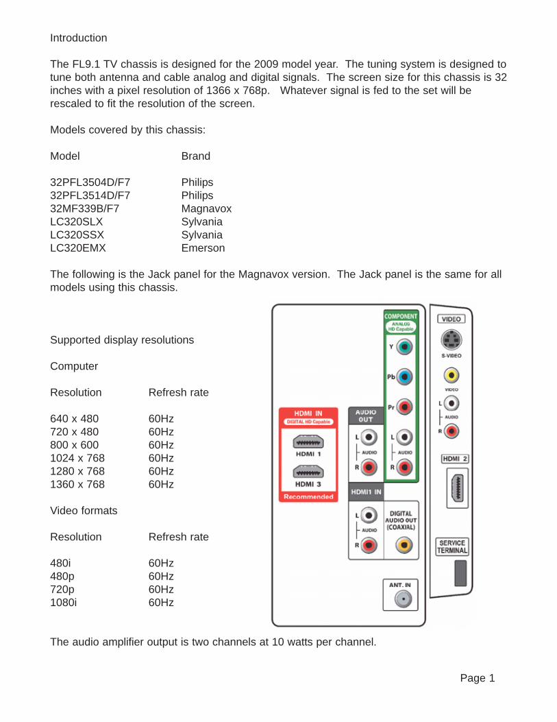
Introduction
The FL9.1 TV chassis is designed for the 2009 model year. The tuning system is designed totune both antenna and cable analog and digital signals. The screen size for this chassis is 32inches with a pixel resolution of 1366 x 768p. Whatever signal is fed to the set will berescaled to fit the resolution of the screen.
Models covered by this chassis:
Model Brand
32PFL3504D/F7 Philips32PFL3514D/F7 Philips32MF339B/F7 MagnavoxLC320SLX SylvaniaLC320SSX SylvaniaLC320EMX Emerson
The following is the Jack panel for the Magnavox version. The Jack panel is the same for allmodels using this chassis.
Supported display resolutions
Computer
Resolution Refresh rate
640 x 480 60Hz720 x 480 60Hz800 x 600 60Hz1024 x 768 60Hz1280 x 768 60Hz1360 x 768 60Hz
Video formats
Resolution Refresh rate
480i 60Hz480p 60Hz720p 60Hz1080i 60Hz
The audio amplifier output is two channels at 10 watts per channel.
Page 1
Connectivity
AV1 Audio L/R in, YPbPrHDMI1 HDMI v1.3, Analog audio L/R inHDMI2 HDMI v1.3
Audio output Digital Coaxial
Side HDMI v1.3, S-video in, CVBS in, Audio L/R in, USB (software upgrade only)
The FL9.1 chassis has the Philips EasyLink (HDMI-CEC) capability. This feature has addi-tional function compared to the 2008 Philips sets. This feature is referred to as CEC in theMagnavox, Sylvania and Emerson products.
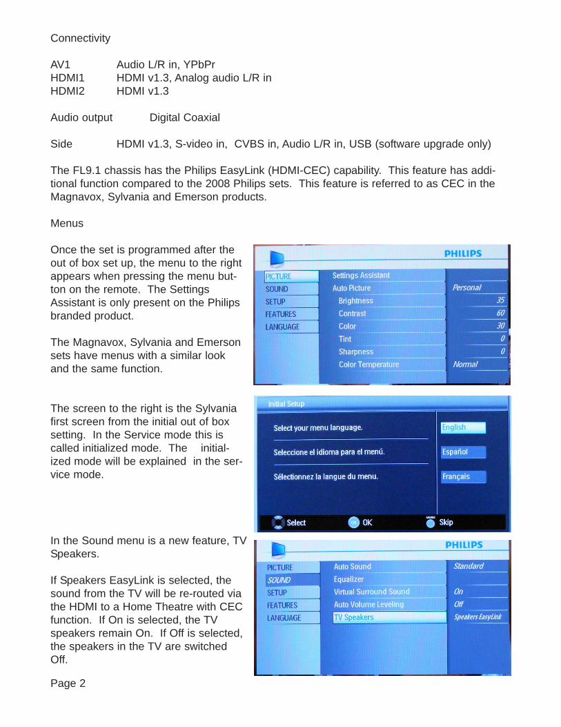
Menus
Once the set is programmed after theout of box set up, the menu to the rightappears when pressing the menu but-ton on the remote. The SettingsAssistant is only present on the Philipsbranded product.
The Magnavox, Sylvania and Emersonsets have menus with a similar lookand the same function.
The screen to the right is the Sylvaniafirst screen from the initial out of boxsetting. In the Service mode this iscalled initialized mode. The initial-ized mode will be explained in the ser-vice mode.
In the Sound menu is a new feature, TVSpeakers.
If Speakers EasyLink is selected, thesound from the TV will be re-routed viathe HDMI to a Home Theatre with CECfunction. If On is selected, the TVspeakers remain On. If Off is selected,the speakers in the TV are switchedOff.
Page 2

Setup Menu
In the Setup Menu, channels can be pro-grammed using Autoprogram. Channelscan be deleted from the channel ringusing Channel List. Add Channels can beused to to add channels not picked upduring Autoprogram. Antenna is onlyavailable in the Antenna mode.
Features
Among other things, Location, Child lock,and Closed Caption can be selected inthe Features menu. This is called theDetails menu in the Magnavox, Sylvaniaand Emerson sets.
Out of box, the Child Lock pin is 0000. Ifthe customer forgets their pin, unpluggingthe set will reset the pin to 0000.
Current Software can also be viewed.
To load new software: (Philips Only)
1. Down the latest version from the customer website *.zip.
2. Unzip the file and extract the *.eccfile and load it in to the root
directory of a USB drive.3. Unplug the TV from AC power.
4. Insert the USB drive into the TV.5. Re-apply power and turn the set On.6. Do not unplug the set on use the remote
while the set is programming as this will damage the TV.
Page 3
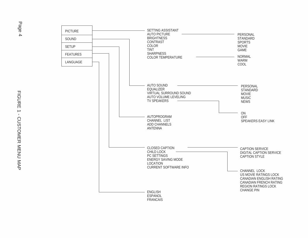
PICTURE
SOUND
SETUP
FEATURES
LANGUAGE
SETTING ASSISTANTAUTO PICTUREBRIGHTNESSCONTRASTCOLORTINTSHARPNESSCOLOR TEMPERATURE
PERSONALSTANDARDSPORTSMOVIEGAME
NORMALWARMCOOL
AUTO SOUNDEQUALIZERVIRTUAL SURROUND SOUNDAUTO VOLUME LEVELINGTV SPEAKERS
AUTOPROGRAMCHANNEL LISTADD CHANNELSANTENNA
CLOSED CAPTIONCHILD LOCKPC SETTINGSENERGY SAVING MODELOCATIONCURRENT SOFTWARE INFO
ENGLISHESPANOLFRANCAIS
PERSONALSTANDARDMOVIEMUSICNEWS
ONOFFSPEAKERS EASY LINK
CAPTION SERVICEDIGITAL CAPTION SERVICECAPTION STYLE
CHANNEL LOCKUS MOVIE RATINGS LOCKCANADIAN ENGLISH RATINGCANADIAN FRENCH RATINGREGION RATINGS LOCKCHANGE PIN
FIGU
RE
1 - CU
STO
ME
R M
EN
U M
AP
Page 4
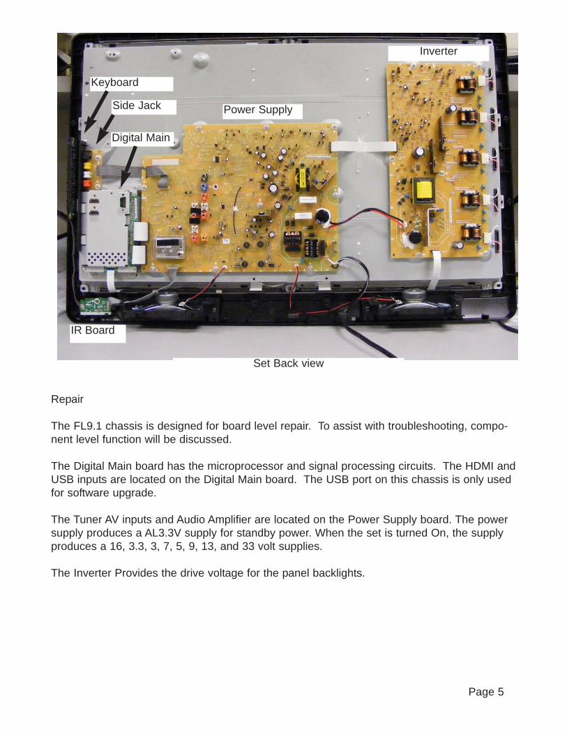
Repair
The FL9.1 chassis is designed for board level repair. To assist with troubleshooting, compo-nent level function will be discussed.
The Digital Main board has the microprocessor and signal processing circuits. The HDMI andUSB inputs are located on the Digital Main board. The USB port on this chassis is only usedfor software upgrade.
The Tuner AV inputs and Audio Amplifier are located on the Power Supply board. The powersupply produces a AL3.3V supply for standby power. When the set is turned On, the supplyproduces a 16, 3.3, 3, 7, 5, 9, 13, and 33 volt supplies.
The Inverter Provides the drive voltage for the panel backlights.
Inverter
Power Supply
Digital Main
IR Board
Keyboard
Side Jack
Set Back view
Page 5
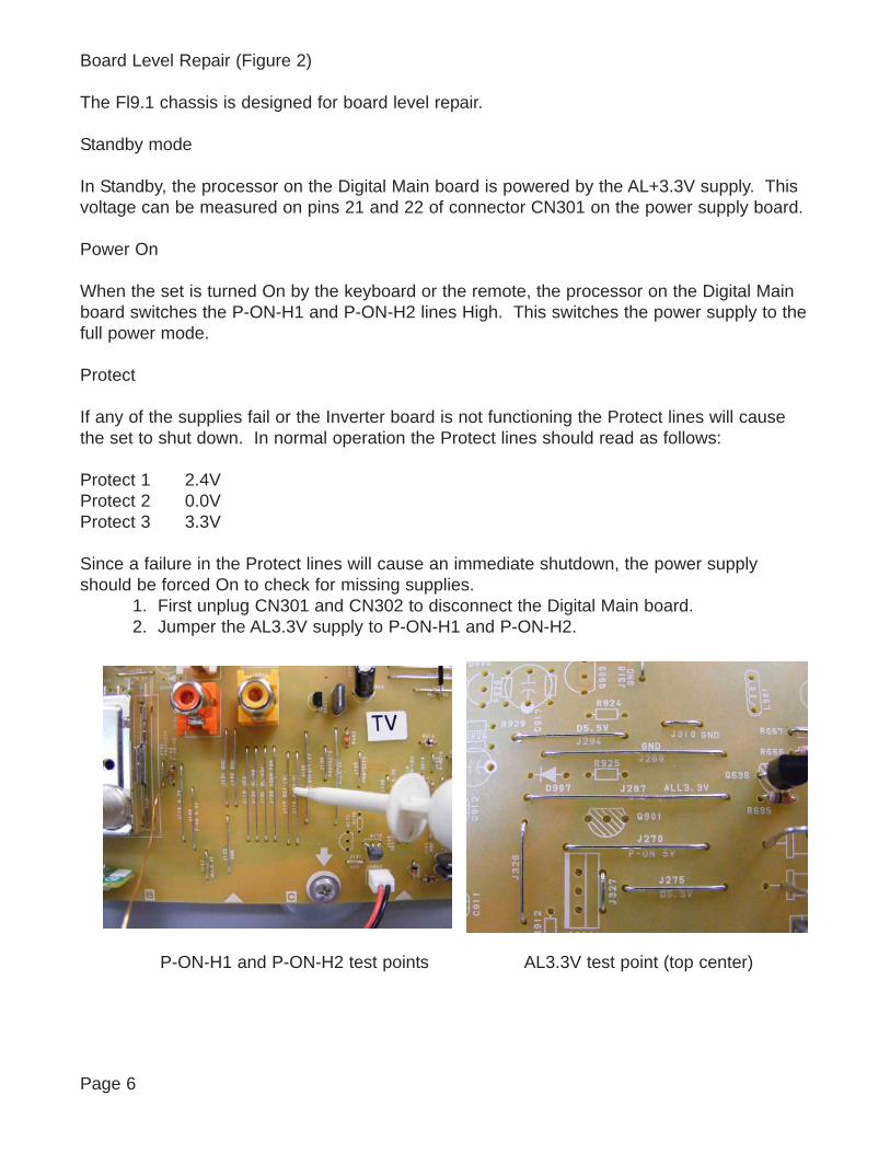
Board Level Repair (Figure 2)
The Fl9.1 chassis is designed for board level repair.
Standby mode
In Standby, the processor on the Digital Main board is powered by the AL+3.3V supply. Thisvoltage can be measured on pins 21 and 22 of connector CN301 on the power supply board.
Power On
When the set is turned On by the keyboard or the remote, the processor on the Digital Mainboard switches the P-ON-H1 and P-ON-H2 lines High. This switches the power supply to thefull power mode.
Protect
If any of the supplies fail or the Inverter board is not functioning the Protect lines will causethe set to shut down. In normal operation the Protect lines should read as follows:
Protect 1 2.4VProtect 2 0.0VProtect 3 3.3V
Since a failure in the Protect lines will cause an immediate shutdown, the power supplyshould be forced On to check for missing supplies.
1. First unplug CN301 and CN302 to disconnect the Digital Main board.2. Jumper the AL3.3V supply to P-ON-H1 and P-ON-H2.
P-ON-H1 and P-ON-H2 test points AL3.3V test point (top center)
Page 6
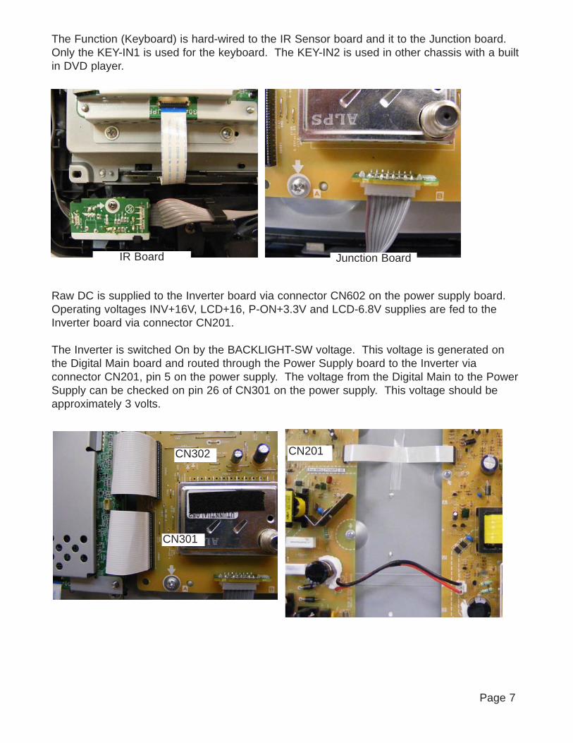
The Function (Keyboard) is hard-wired to the IR Sensor board and it to the Junction board.Only the KEY-IN1 is used for the keyboard. The KEY-IN2 is used in other chassis with a builtin DVD player.
Raw DC is supplied to the Inverter board via connector CN602 on the power supply board.Operating voltages INV+16V, LCD+16, P-ON+3.3V and LCD-6.8V supplies are fed to theInverter board via connector CN201.
The Inverter is switched On by the BACKLIGHT-SW voltage. This voltage is generated onthe Digital Main board and routed through the Power Supply board to the Inverter viaconnector CN201, pin 5 on the power supply. The voltage from the Digital Main to the PowerSupply can be checked on pin 26 of CN301 on the power supply. This voltage should beapproximately 3 volts.
IR Board Junction Board
CN302
CN301
CN201
Page 7
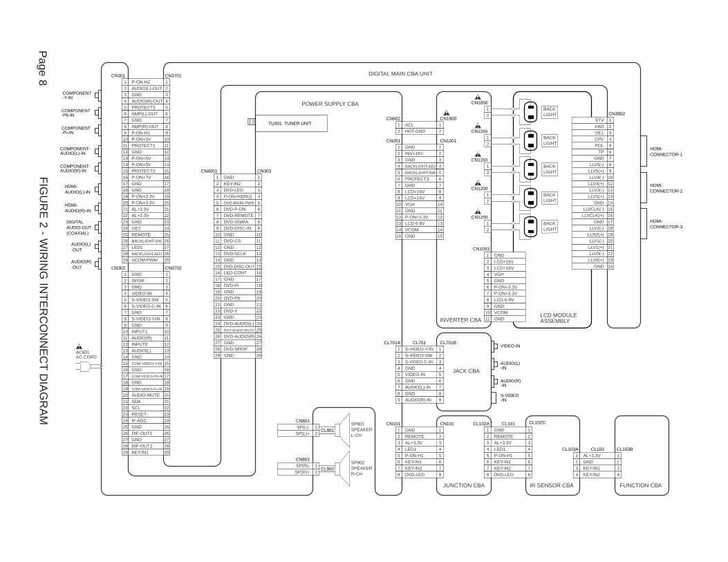
INVERTER CBA
TU301 TUNER UNIT
HDMI-AUDIO(L)-IN
HDMI-AUDIO(R)-IN
AUDIO(L)-OUT
AUDIO(R)-OUT
AC601AC CORD
POWER SUPPLY CBA
DIGITAL MAIN CBA UNIT
HDMI-CONNECTOR-1
HDMI-CONNECTOR-2
HDMI-CONNECTOR-3
LCD MODULEASSEMBLY
CL8011
CN801
2SP(L)-SP(L)+
CL8021
CN802
2SP(R)-SP(R)+
SP801SPEAKERL-CH
SP802SPEAKERR-CH
COMPONENT-Y-IN
COMPONENT-Pb-IN
COMPONENT-Pr-IN
COMPONENT-AUDIO(L)-IN
COMPONENT-AUDIO(R)-IN
VIDEO-IN
AUDIO(L)-IN
AUDIO(R)-IN
S-VIDEO-IN
CN602
CN201
CN1900
CN1001
22 HOT-GND11 ACL
11 GND22 INV+16V33 GND44 BACKLIGHT-ADJ55 BACKLIGHT-SW66 PROTECT377 GND88 LCD+16V99 LCD+16V1010 VGH1111 GND1212 P-ON+3.3V1313 LCD-6.8V1414 VCOM1515 GND
BACKLIGHT
CN1050
21
BACKLIGHT
CN1100
21
BACKLIGHT
CN1150
21
BACKLIGHT
CN1200
21
BACKLIGHT
CN1250
21DIGITAL
AUDIO-OUT(COAXIAL)
JACK CBA
JUNCTION CBA IR SENSOR CBA FUNCTION CBA
CL701A CL701 CL701B11 S-VIDEO-Y-IN
33 S-VIDEO-C-IN22 S-VIDEO-SW
44 GND55 VIDEO-IN
77 AUDIO(L)-IN66 GND
88 GND99 AUDIO(R)-IN
101LC101NC
CL103
CN10111 GND
33 AL+3.3V22 REMOTE
44 LED155 P-ON-H166 KEY-IN177 KEY-IN288 DVD-LED
11 GND
33 AL+3.3V22 REMOTE
44 LED1
44 KEY-IN2
55 P-ON-H166 KEY-IN177 KEY-IN288 DVD-LED
CL102CCL102A
CL103BCL103A
33 KEY-IN122 GND11 AL+3.3V
CN1003
11 GND10 VCOM9 GND8 LCD-6.8V7 P-ON+3.3V6 P-ON+3.3V5 GND4 VGH3 LCD+16V2 LCD+16V1 GND
CN3902
24GND23LLV0(+)22LLV0(-)21LLV1(+)20LLV1(-)19LLN2(+)18LLV2(-)17GND16LLVCLK(+)15LLVCLK(-)14GND13LLV3(+)12LLV3(-)11LLV4(+)10LLV4(-)9LLV5(+)8LLV5(-)7GND6TP5POL4CPV3OE12XAO1STV
CN3701CN301
23
19
21
15
17
22
20
18
16
14
10
12
6
8
13
11
9
7
5
1
34
1
5
3
9
7
2
4
6
8
10
14
12
18
16
11
13
15
17
19
23
2120
2P-ON-H2AUDIO(L)-OUTGNDAUDIO(R)-OUTPROTECT3AMP(L)-OUTGNDAMP(R)-OUTP-ON-H1P-ON+3VPROTECT1GNDP-ON+5VP-ON+5VPROTECT2P-ON+7VGNDGNDP-ON+3.3VP-ON+3.3VAL+3.3VAL+3.3VGND
22
2424 OE22525 REMOTE2626 BACKLIGHT-SW2727 LED12828 BACKLIGHT-ADJ2929 VCOM-PWM
CN3702CN302
23
19
21
15
17
22
20
18
16
14
10
12
6
8
13
11
9
7
5
1
34
1
5
3
9
7
2
4
6
8
10
14
12
18
16
11
13
15
17
19
23
2120
2GNDSPDIFGNDVIDEO-INS-VIDEO-SWS-VIDEO-C-INGNDS-VIDEO-Y-INGNDINPUT1AUDIO(R)INPUT0AUDIO(L)GNDCOM-VIDEO-Y-IN
GNDCOM-VIDEO-Pb-IN
GNDCOM-VIDEO-Pr-IN
AUDIO-MUTESDASCLRESET
22
2424 IF-AGC2525 GND2626 DIF-OUT12727 GND2828 DIF-OUT22929 KEY-IN1
CN303CN4001
23
19
21
15
17
22
20
18
16
14
10
12
6
8
13
11
9
7
5
1
34
1
5
3
9
7
2
4
6
8
10
14
12
18
16
11
13
15
17
19
23
2120
2GNDKEY-IN2DVD-LEDP-ON-H3(NU)DVD-MAIN-PWRDVD-P-ONDVD-REMOTEDVD-SDATADVD-DISC-INGNDDVD-CSGNDDVD-SCLKGNDDVD-DISC-OUTLED-CONTGNDDVD-PrGNDDVD-PbGNDDVD-YGND
22
2424 DVD-AUDIO(L)2525 DVD-AUDIO-MUTE
2626 DVD-AUDIO(R)2727 GND2828 DVD-SPDIF2929 GND
FIGU
RE
2 - WIR
ING
INTE
RC
ON
NE
CT
DIA
GR
AM
Page 8
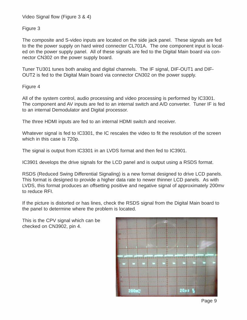
Video Signal flow (Figure 3 & 4)
Figure 3
The composite and S-video inputs are located on the side jack panel. These signals are fedto the the power supply on hard wired connecter CL701A. The one component input is locat-ed on the power supply panel. All of these signals are fed to the Digital Main board via con-nector CN302 on the power supply board.
Tuner TU301 tunes both analog and digital channels. The IF signal, DIF-OUT1 and DIF-OUT2 is fed to the Digital Main board via connector CN302 on the power supply.
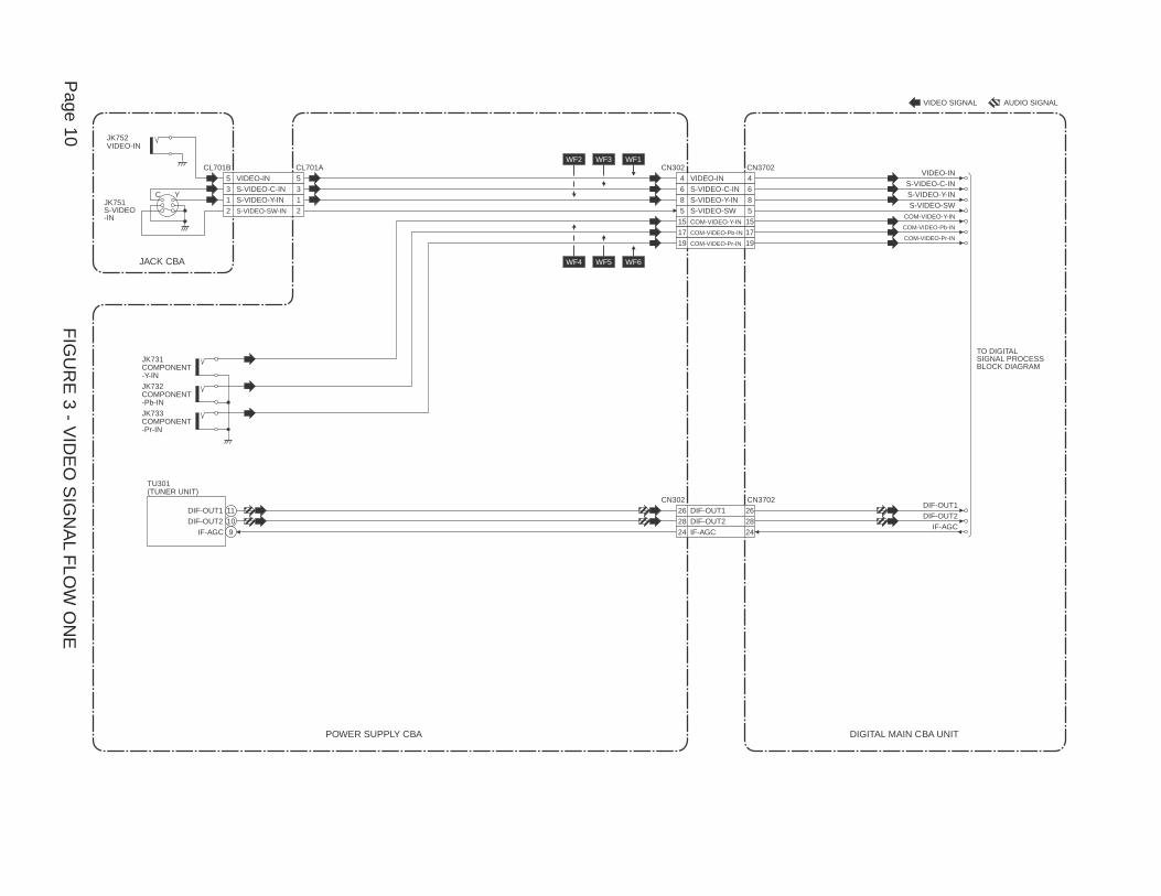
Figure 4
All of the system control, audio processing and video processing is performed by IC3301.The component and AV inputs are fed to an internal switch and A/D converter. Tuner IF is fedto an internal Demodulator and Digital processor.
The three HDMI inputs are fed to an internal HDMI switch and receiver.
Whatever signal is fed to IC3301, the IC rescales the video to fit the resolution of the screenwhich in this case is 720p.
The signal is output from IC3301 in an LVDS format and then fed to IC3901.
IC3901 develops the drive signals for the LCD panel and is output using a RSDS format.
RSDS (Reduced Swing Differential Signaling) is a new format designed to drive LCD panels.This format is designed to provide a higher data rate to newer thinner LCD panels. As withLVDS, this format produces an offsetting positive and negative signal of approximately 200mvto reduce RFI.
If the picture is distorted or has lines, check the RSDS signal from the Digital Main board tothe panel to determine where the problem is located.
This is the CPV signal which can bechecked on CN3902, pin 4.
Page 9
DIGITAL MAIN CBA UNIT
COMPONENT-Y-IN
COMPONENT-Pb-IN
COMPONENT-Pr-IN
JK731
JK732
JK733
VIDEO-IN4 4S-VIDEO-C-IN6 6S-VIDEO-Y-IN8 8S-VIDEO-SW5 5COM-VIDEO-Y-IN15 15COM-VIDEO-Pb-IN17 17COM-VIDEO-Pr-IN19 19
JACK CBA
CL701A CL701BVIDEO-IN 5S-VIDEO-C-IN 3S-VIDEO-Y-IN 1
531JK751
S-VIDEO-IN
C Y
JK752VIDEO-IN
S-VIDEO-SW-IN 22
POWER SUPPLY CBA
TU301
DIF-OUT1 11DIF-OUT2 10
(TUNER UNIT)
IF-AGC 9
CN302 CN3702DIF-OUT126 26
IF-AGC24 24DIF-OUT228 28
DIF-OUT1DIF-OUT2
IF-AGC
CN302 CN3702VIDEO-IN
S-VIDEO-C-INS-VIDEO-Y-INS-VIDEO-SW
COM-VIDEO-Y-IN
COM-VIDEO-Pr-IN
COM-VIDEO-Pb-IN
TO DIGITALSIGNAL PROCESSBLOCK DIAGRAM
WF1WF2 WF3
WF4 WF5 WF6
VIDEO SIGNAL AUDIO SIGNAL
FIGU
RE
3 - VID
EO
SIG
NA
LFLO
W O
NE
Page 10
DIG
ITA
L M
AIN
CBA
UN
ITIC
3301
(DIG
ITA
L S
IGN
AL
PR
OC
ES
S)
IC39
01 (T
ININ
G C
ON
TRO
LLE
R)
LCD
MO
DU
LEA
SS
EM
BLY
CN
3902
LLV
1P21
LLV
1N20
LLV
0P23
LLV
0N22
LLV
2P19
LLV
2N18
LLV
3P13
LLV
3N12
LLV
4P11
LLV
4N10
LLV
5P9
LLV
5N8
LLV
CLK
P16
LLV
CLK
N15
TP6
PO
L5
CP
V4
OE
3S
TV1
27 26 29 28 31 30 42 41 45 44 47 46 33 32 88 19 92 93 94
123
122
125
124
127
126
131
130
129
128
LCD
TIM
ING
CO
NTR
OLL
ER
LVD
SR
X
RS
DS
I/F
FRC
CO
LOR
PR
OO
F
ADV
AN
CE
OV
ER
DR
IVE
FAIL
SA
FE M
OD
E
AD
23
AD
24
AE
23
AF2
3
AF2
2
AE
22
AD
21
AD
22
AF2
4
AE
24
LVD
STX
DIG
ITA
LS
IGN
AL
PR
OC
ES
S
A/D
CO
NV
ER
TER
S-V
IDE
O-Y
-INS
W
V1
U2
U1
S-V
IDE
O-C
-IN
U3
VID
EO
-IN
V3
CO
M-V
IDE
O-P
r-IN
CO
M-V
IDE
O-P
b-IN
CO
M-V
IDE
O-Y
-IN
AA
3
IF-A
GC
HD
MI-I
N1
HD
MI-I
N2
JK37
01
TMD
S-D
0(+)
TMD
S-D
0(-)
TMD
S-D
1(+)
TMD
S-D
1(-)
TMD
S-D
2(+)
TMD
S-D
2(-)
SD
AS
CL
7 9 4 6 1 3 10 12 16 15 7 9 4 6 1 3 10 12 16 15
JK37
02
TMD
S-D
0(+)
TMD
S-D
0(-)
TMD
S-D
1(+)
TMD
S-D
1(-)
TMD
S-D
2(+)
TMD
S-D
2(-)
TMD
S-C
LOC
K(+
)TM
DS
-CLO
CK
(-)
SD
AS
CL
A9
B9
C8
C9
B8
A8
B10
A10
A11
B11 A5
B5
C4
C5
B4
A4
B6
A6
A7
B7
TMD
S-C
LOC
K(+
)TM
DS
-CLO
CK
(-)
DE
MO
DU
LATO
R/M
PE
G D
EC
OD
ER
AE
2
AF7
AUD
IO I/
F
TO A
UD
IOB
LOC
K D
IAG
RA
MAC
LK
AD
ATA
1
BC
LKLR
CLK
AD
ATA
0S
PD
IF
AD
14
AD
9
AD
12
AD
10
AD
11
AC10
DAT
A(0
-15)
AD
DE
SS
(0-1
2)
IC32
01
A13
-15,
A18
,A
21-2
3,B
13-1
5,B
17,B
19-2
3
C15
,C17
-19,
C23
,C24
,D14
,D
15,D
17-1
9,D
22,D
23
B1,
B9,
C2,
C8,
D1,
D3,
D7,
D9,
F1,F
9,G
2,G
8,H
1,H
3,H
7,H
9
M2,
M3,
M7,
M8,
N2,
N3,
N7,
N8,
P2,
P3,
P7,
P8,
R2
(DD
R2
SD
RA
M)
HD
MI
I/F
HD
MI-I
N3
7 9 4 6 1 3 10 12 16 15
JK37
03
TMD
S-D
0(+)
TMD
S-D
0(-)
TMD
S-D
1(+)
TMD
S-D
1(-)
TMD
S-D
2(+)
TMD
S-D
2(-)
TMD
S-C
LOC
K(+
)TM
DS
-CLO
CK
(-)
SD
AS
CL
B1
B2
C1
C2
D1
D2
A1
A2
A3
B3
AUD
IOD
EC
OD
ER
DIF
-OU
T1D
IF-O
UT2
IF-A
GC
TO V
IDE
OB
LOC
K D
IAG
RA
M
TO V
IDE
OB
LOC
K D
IAG
RA
M
VID
EO
DE
CO
DE
R
AF2
S-V
IDE
O-S
WC
6S
-VID
EO
-SW
M2
AUD
IO(R
)M
1AU
DIO
(L)
VID
EO
SIG
NA
LA
UD
IO S
IGN
AL
FIGURE 4 - VIDEO SIGNAL FLOW TWO Page 11
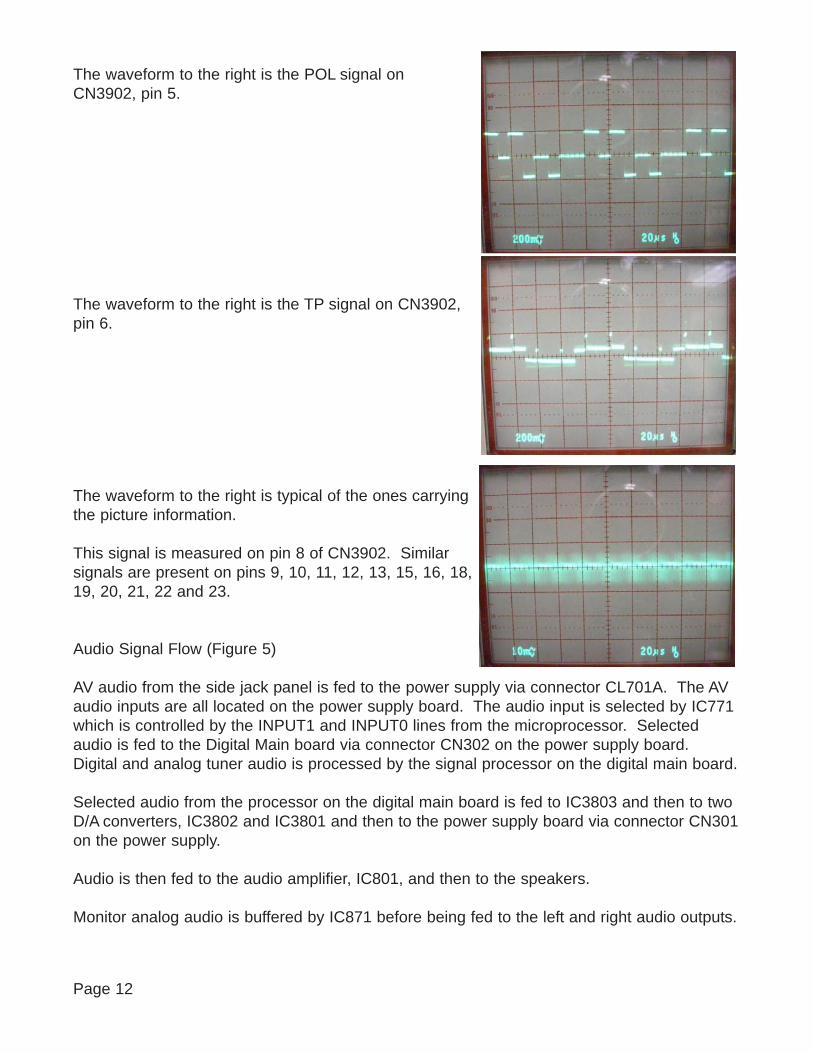
The waveform to the right is the POL signal onCN3902, pin 5.
The waveform to the right is the TP signal on CN3902,pin 6.
The waveform to the right is typical of the ones carryingthe picture information.
This signal is measured on pin 8 of CN3902. Similarsignals are present on pins 9, 10, 11, 12, 13, 15, 16, 18,19, 20, 21, 22 and 23.
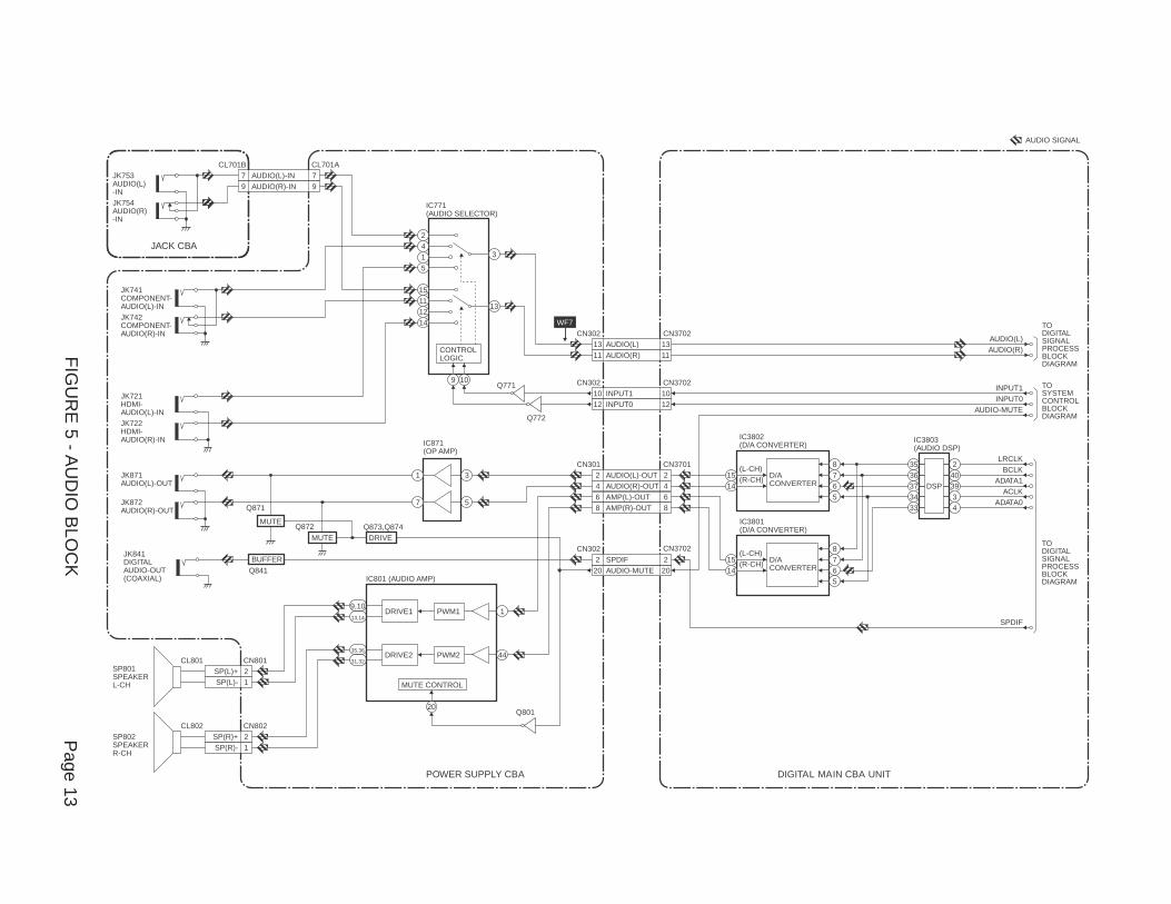
Audio Signal Flow (Figure 5)
AV audio from the side jack panel is fed to the power supply via connector CL701A. The AVaudio inputs are all located on the power supply board. The audio input is selected by IC771which is controlled by the INPUT1 and INPUT0 lines from the microprocessor. Selectedaudio is fed to the Digital Main board via connector CN302 on the power supply board.Digital and analog tuner audio is processed by the signal processor on the digital main board.
Selected audio from the processor on the digital main board is fed to IC3803 and then to twoD/A converters, IC3802 and IC3801 and then to the power supply board via connector CN301on the power supply.
Audio is then fed to the audio amplifier, IC801, and then to the speakers.
Monitor analog audio is buffered by IC871 before being fed to the left and right audio outputs.
Page 12
IC771(AUDIO SELECTOR)
AUDIO(L)-OUT
AUDIO(R)-OUT
HDMI-AUDIO(L)-IN
HDMI-AUDIO(R)-IN
JK721
JK722
JK871
JK872
COMPONENT-AUDIO(L)-IN
COMPONENT-AUDIO(R)-IN
JK741
JK742
2415
15111214
JACK CBA
CL701ACL701BAUDIO(L)-IN 77AUDIO(R)-IN 99AUDIO(L)
-IN
AUDIO(R)-IN
JK753
JK754
CN3702CN302AUDIO(L)13 13AUDIO(R)11 11
CN3702CN302INPUT110 10INPUT012 12
CN3701CN301AUDIO(L)-OUT2 2AUDIO(R)-OUT4 4AMP(L)-OUT6 6AMP(R)-OUT8 8
TINU ABC NIAM LATIGIDABC YLPPUS REWOP
20
IC801 (AUDIO AMP)
1
44
9,1013,14
35,36
31,32
MUTE CONTROL
CN801CL801SP801SPEAKERL-CH
CN802
SP(R)- 1
CL802SP802SPEAKERR-CH
PWM1
PWM2
DRIVE1
CN302 CN3702
AUDIO-MUTE 2020
JK841DIGITALAUDIO-OUT(COAXIAL)
Q841
Q771
Q772
BUFFER
Q871
Q873,Q874MUTE Q872
MUTE
SPDIF 22
SP(R)+ 2
SP(L)- 1SP(L)+ 2
Q801
CONTROL LOGIC
3
109
13
IC871 (OP AMP)
1 3
7 5
DRIVE2
DRIVE
IC3802(D/A CONVERTER)
D/ACONVERTER
1514
8765
(L-CH)(R-CH)
IC3801(D/A CONVERTER)
D/ACONVERTER
1514
8765
(L-CH)(R-CH)
AUDIO(L)AUDIO(R)
TO DIGITALSIGNALPROCESSBLOCKDIAGRAM
TO DIGITALSIGNALPROCESSBLOCKDIAGRAM
INPUT1
LRCLKBCLK
ADATA1ACLK
SPDIF
ADATA0
INPUT0AUDIO-MUTE
TO SYSTEMCONTROLBLOCKDIAGRAM
AUDIO SIGNAL
WF7
3334373635
4339402
(AUDIO DSP)IC3803
DSP
FIGU
RE
5 - AU
DIO
BLO
CK
Page 13
HOT COLDPOWER SUPPLY CBA
HOT CIRCUIT. BE CAREFUL.
Q602SWITCHINGCONTROL
14
3 2
IC601
T601
TO INVERTERBLOCK DIAGRAM (CN1900)
CN602
3
HOT-GND1ACL2
LINEFILTER
L601AC601AC CORD
BRIDGERECTIFIER
D601- D604
5
4
11
14
12
17
18
13
16
15
199
7
8
FEEDBACK
Q601SWITCHING
Q631
CN201 CN1001
CN301 CN3701
Q207,Q208SWITCHING
Q211SW-6.8V
SW
Q401
Q209,D204SW+16V
Q635IC631
+3.3VREG. 23
Q634
Q638,Q639
Q641,643SW+5V
Q640SW+5V
Q642SW+9V
Q501SW+16V
Q637,D666SW+3.3V
LINEFILTER
L602
4A/125V
F601 4A/125V
P-ON-H1TO SYSTEM CONTROL BLOCKDIAGRAM
P-ON-H2
+5V REG.
PROTECT2PROTECT1
SWITCHING
AL+33VP-ON+5V
AL+3.3V
AL+13VTUNER+5V
P-ON+9V
19,20
12
28,9
21,22
13,14
LCD+16VLCD+6.8V
INV+16VVGHP-ON+3.3V
P-ON+3VP-ON+7VAL+3.3VP-ON+3.3VP-ON+5V
INVERTER CBA
DIGITAL MAIN CBA UNIT
13LCD-6.8V13
P-ON+3.3V19,20
P-ON+3.3V1210VGH10
INV+16V2LCD+16V8,9
AL+3.3V21,221610
P-ON+7V16P-ON+3V10
P-ON+5V13,14
Q210 Q201,Q212SW+24.5V
CAUTION !Fixed voltage (or Auto voltage selectable) power supply circuit is used in this unit.If Main Fuse (F601) is blown , check to see that all components in the power supplycircuit are not defective before you connect the AC plug to the AC power supply.Otherwise it may cause some components in the power supply circuit to fail.
For continued protection against risk of fire, replace only with same type 4 A, 125V fuse.
CAUTION ! :
ATTENTION : Utiliser un fusible de rechange de mŒme type de 4A, 125V.4A/125V
NOTE:The voltage for parts in hot circuit is measured usinghot GND as a common terminal.
FIGU
RE
6 - PO
WE
R S
UP
PLY
Page 14
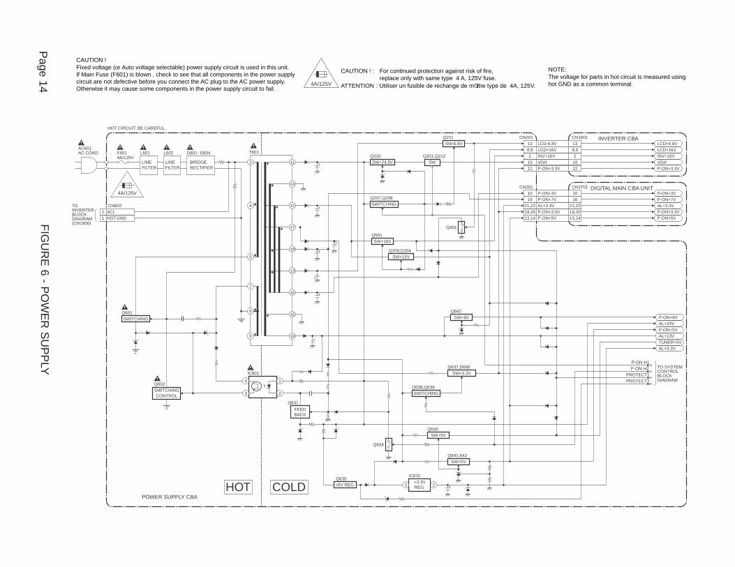
Power Supply (Figure 6)
AC is fed the line filters and bridge rectifier. RAW DC is fed to the Inverter via connectorCN602 on the power supply board and to transformer T601.
The switch mode supply consist of transistors Q601 and Q602. In standby, the power supplyis running in a low power pulsating mode controlled by Q634 on the secondary side.
When the set is turned On, the P-ON-H1 and P-ON-H2 lines goes High. P-ON-H2 changesturns on transistor Q634 to change the bias of the feed back circuit switching the power sup-ply to a full power mode. It also turns on transistors Q638, Q639 and Q637 to turn the P-ON-3.3V supply On. The P-ON-H1 line switches Q207 and Q208. This switches Q210, Q201and Q212 to switch the VGH voltages. Q211 is turned On switching the LCD-6.8V supply. Italso switches Q209 switching the LCD+16V supply. Q501 is switched to turn on the INV+16Vsupply. Q642 is switched to produce the P-ON+9V supply.
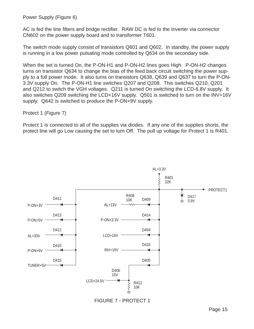
Protect 1 (Figure 7)
Protect 1 is connected to all of the supplies via diodes. If any one of the supplies shorts, theprotect line will go Low causing the set to turn Off. The pull up voltage for Protect 1 is R401.
Page 15
P-ON+3V
P-ON+5V
AL+33V
P-ON+9V
TUNER+5V
D409
D414
D404
D416
D405
R40810K
AL+13V
P-ON+3.3V
LCD+16V
INV+16V
LCD+24.5V R41210K
D40615V
D411
D413
D412
D410
D415
AL+3.3V
R40122K
D4173.9V
PROTECT1
FIGURE 7 - PROTECT 1
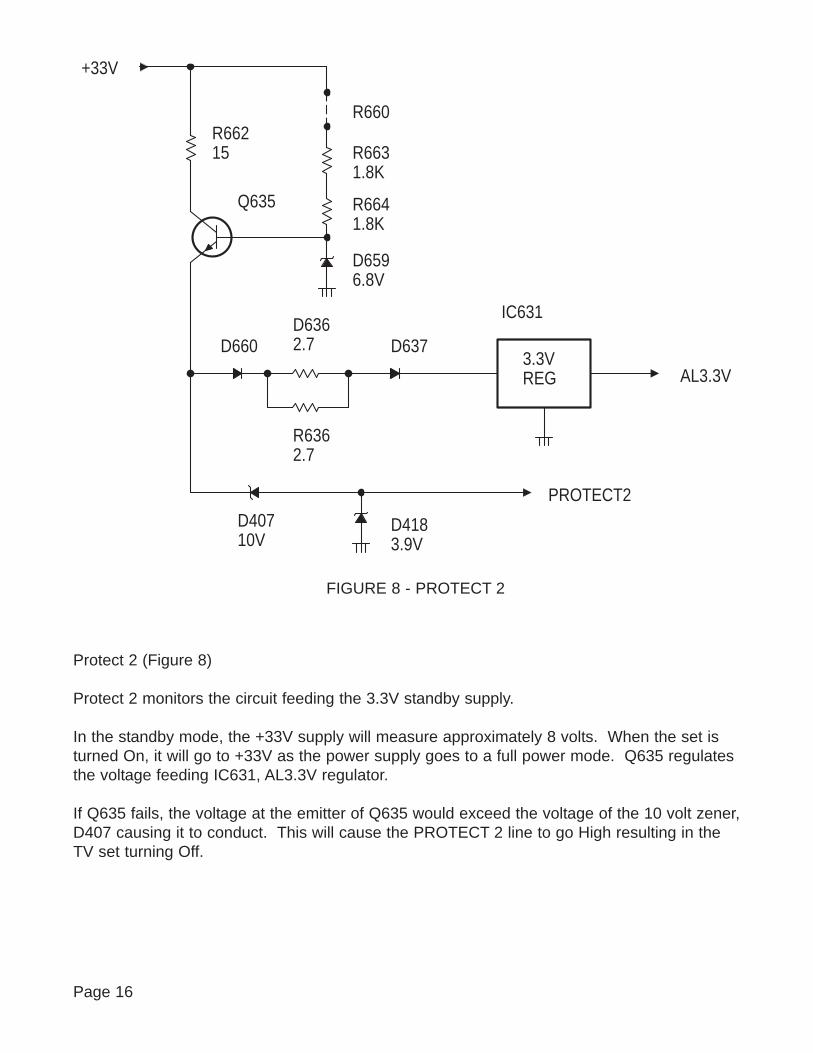
Protect 2 (Figure 8)
Protect 2 monitors the circuit feeding the 3.3V standby supply.
In the standby mode, the +33V supply will measure approximately 8 volts. When the set isturned On, it will go to +33V as the power supply goes to a full power mode. Q635 regulatesthe voltage feeding IC631, AL3.3V regulator.
If Q635 fails, the voltage at the emitter of Q635 would exceed the voltage of the 10 volt zener,D407 causing it to conduct. This will cause the PROTECT 2 line to go High resulting in theTV set turning Off.
3.3VREG
D660D6362.7
R6362.7
D637
IC631
AL3.3V
D40710V
D4183.9V
PROTECT2
R66215
R660
R6631.8K
R6641.8K
D6596.8V
Q635
+33V
FIGURE 8 - PROTECT 2
Page 16
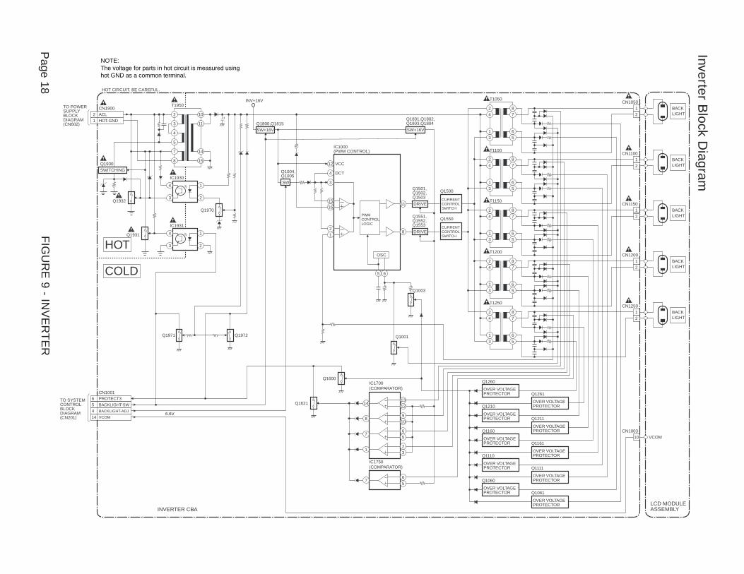
Inverter (Figure 9)
The inverter power supply is switched On by the BACKLIGHT-SW line from the digital board.The BACKLIGHT-ADJ line is fed to IC1000 to control the pulse width output of IC1000 andthe brightness of the backlight. The outputs to the backlights are fed to over voltage protec-tion circuits. If a problem is detected in one of the outputs, Q1600 is turned On causing theProtect 3 line to go Low. This will cause the set to turn Off.
System Control (Figure 10)
Control signals from the Function board and IR Sensor board are routed through the powersupply board to IC3301. IC3301 preforms all of the system control functions.
Note that the P-ON-HI voltage in pin 5 of CN101 is inverted from the pin with the same label,CN301, pin 9.
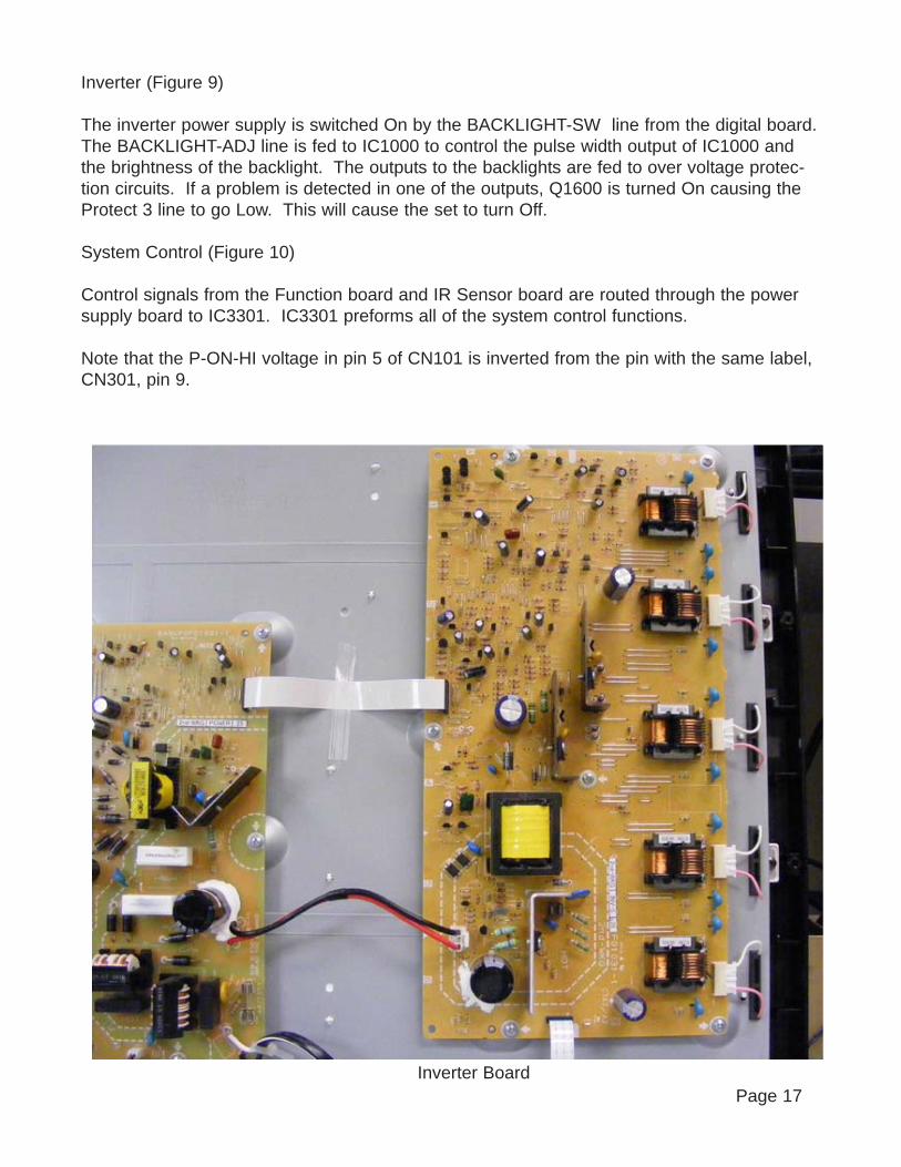
Inverter BoardPage 17
Inverter Block D
iagram
INVERTER CBA
CN1001 PROTECT36
BACKLIGHT-ADJ4VCOM14
BACKLIGHT-SW5TO SYSTEMCONTROLBLOCK DIAGRAM(CN201)
T1950
10
11
14
15
2
3
4
5
7
8
14
3 2
Q1970
Q1971
IC1930
14
3 2
IC1931
Q1931
TO POWERSUPPLY BLOCK DIAGRAM(CN602)
HOT
COLD
HOT CIRCUIT. BE CAREFUL.
Q1972
SWITCHINGQ1930
CN1900
Q1932
IC1000 (PWM CONTROL)
BACKLIGHT
12
12
12
CN1100
CN1150
CN1200
BACKLIGHT
BACKLIGHT
T1100
Q1551, Q1552, Q1553
Q1001
Q1003
Q1210
Q1211
Q1160
Q1161
Q1110
Q1111
Q1500
Q1801,Q1802, Q1803,Q1804Q1800,Q1815
Q1004,Q1005
Q1550
T1150
4
13
78
65
2
T1200
DRIVE
Q1501, Q1502, Q1503
DRIVE
OSC
PWMCONTROLLOGIC
VCC
DCT
CURRENTCONTROLSWITCH
CURRENTCONTROLSWITCH
OVER VOLTAGEPROTECTOR
Q1260
OVER VOLTAGEPROTECTOR
OVER VOLTAGEPROTECTOR
Q1261
OVER VOLTAGEPROTECTOR
OVER VOLTAGEPROTECTOR
OVER VOLTAGEPROTECTOR
OVER VOLTAGEPROTECTOR
OVER VOLTAGEPROTECTORQ1060
OVER VOLTAGEPROTECTOR Q1061
OVER VOLTAGEPROTECTOR
11
8
5 6
15
3
4
12
16
21
SW+16V
SW
SW+16V
Q1600
Q1621
LCD MODULEASSEMBLY
T1050
4
13
78
65
2
4
13
78
65
2
4
13
78
65
2
T1250
4
13
78
65
2
BACKLIGHT
12
CN1050
IC1700 (COMPARATOR)
IC1750(COMPARATOR)
67
5
23
910
1
8
1312
14
67
5
ACL2HOT-GND1
INV+16V
10CN1003
VCOM
12
CN1250BACKLIGHT
NOTE:The voltage for parts in hot circuit is measured usinghot GND as a common terminal.
6.6V
FIGU
RE
9 - INV
ER
TER
P
age 18

AC18
KEY SWITCH
IC3301(MAIN MICRO CONTROLLER)
DIGITAL MAIN CBA UNIT
IR SENSOR CBAFUNCTION CBA
POWER SUPPLY CBA
CL102C
REMOTESENSOR
RS101
AL+6.0V
POWERD101CL102A
CL103B
REMOTE2 2P-ON-H15 5
CN302CN3702
CN3702 CN302
CLKOUTCLKIN
X310125MHzOSC
N1N2
SCLSDA
45
TU301 (TUNER UNIT)
TO INVERTERBLOCK DIAGRAM(CN1001)
TO POWER SUPPLY BLOCK DIAGRAM
PROTECT3 AE5VCOM-PWM AC14
PROTECT2 AD4PROTECT1 AD5
KEY-IN1 AC5
BACKLIGHT-SW AB16
E1E2
P-ON-H2 AB13
REMOTE R22
P-ON-H1
PROTECT2PROTECT1
P-ON-H2P-ON-H1
R23
JUNCTION CBA
CN101
KEY-IN16 6
CL103AKEY-IN13 3
CN201
CN101
CN301
Q172
CN3701
AB23BACKLIGHT-ADJ
IC3101 (MEMORY)
SCKSI
SO
AB25
AB24
AC25
AC24
6521
E113
AC19
SCLSDA
CN301CN3701
CSWP
SCKSINSOUTCSWP
IC201,Q203,Q204,Q205
DRIVE
22 22SCL21 21SDA
11 11PROTECT115 15PROTECT25 5PROTECT329 29VCOM-PWM26 26BACKLIGHT-SW
28 28BACKLIGHT-ADJ
KEY-IN129 29
P-ON-H19 9
REMOTE25 25P-ON-H21 1
REMOTE2 2P-ON-H15 5KEY-IN16 6
6 PROTECT35 BACKLIGHT-SW
4 BACKLIGHT-ADJ
14 VCOM
TO AUDIOBLOCK DIAGRAM AUDIO-MUTE
INPUT0INPUT1
AUDIO-MUTE
INPUT0INPUT1
AB9
88 DVD-LED 88 DVD-LED
FIGU
RE
10 - SY
STE
M C
ON
TRO
LP
age 19
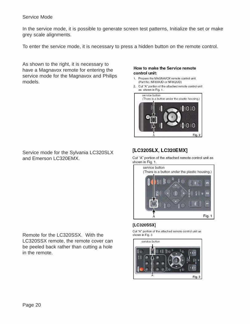
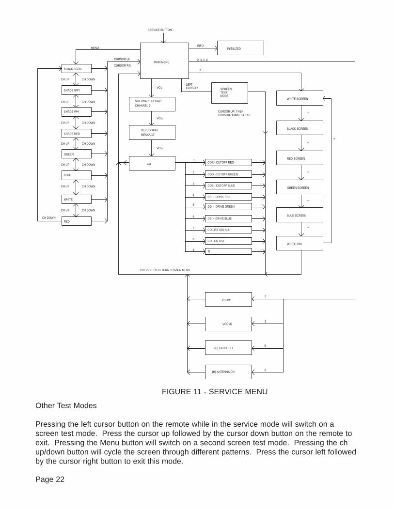
Service Mode
In the service mode, it is possible to generate screen test patterns, Initialize the set or makegrey scale alignments.
To enter the service mode, it is necessary to press a hidden button on the remote control.
As shown to the right, it is necessary tohave a Magnavox remote for entering theservice mode for the Magnavox and Philipsmodels.
Service mode for the Sylvania LC320SLXand Emerson LC320EMX.
Remote for the LC320SSX. With theLC320SSX remote, the remote cover canbe peeled back rather than cutting a holein the remote.
Page 20
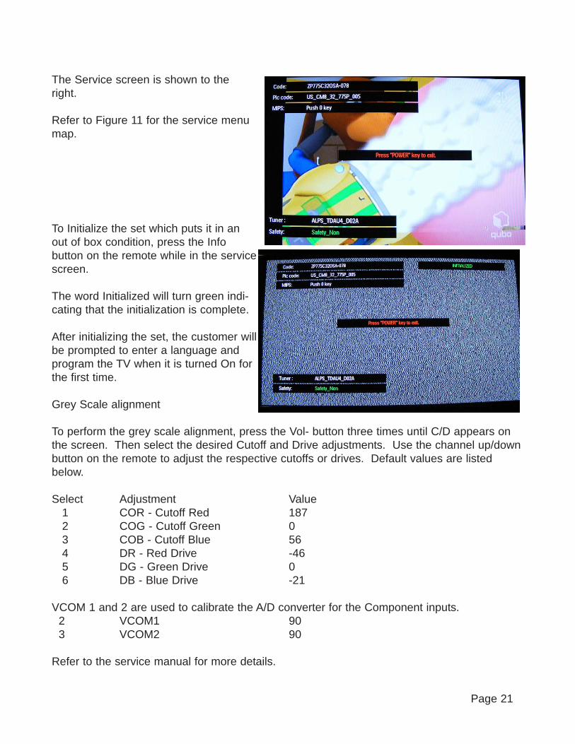
The Service screen is shown to the right.
Refer to Figure 11 for the service menumap.
To Initialize the set which puts it in anout of box condition, press the Infobutton on the remote while in the servicescreen.
The word Initialized will turn green indi-cating that the initialization is complete.
After initializing the set, the customer willbe prompted to enter a language andprogram the TV when it is turned On forthe first time.
Grey Scale alignment
To perform the grey scale alignment, press the Vol- button three times until C/D appears onthe screen. Then select the desired Cutoff and Drive adjustments. Use the channel up/downbutton on the remote to adjust the respective cutoffs or drives. Default values are listedbelow.
Select Adjustment Value1 COR - Cutoff Red 1872 COG - Cutoff Green 03 COB - Cutoff Blue 564 DR - Red Drive -465 DG - Green Drive 06 DB - Blue Drive -21
VCOM 1 and 2 are used to calibrate the A/D converter for the Component inputs.2 VCOM1 903 VCOM2 90
Refer to the service manual for more details.
Page 21
SERVICE BUTTON
SOFTWARE UPDATE
CD COR - CUTOFF RED1
VOL-
VOL-
VOL-
INITILIZEDINFO
7
7
7
7
WHITE SCREEN
BLACK SCREEN
RED SCREEN
GREEN SCREEN
VCOM1
VCOM2
(H) CABLE CH
(H) ANTENNA CH
2, 3, 5, 6MAIN MENU
2
3
5
6
7
BLUE SCREEN
WHITE 20%
COG - CUTOFF GREEN
COB - CUTOFF BLUE
DR - DRIVE RED
CO - DR LIST
CO LIST ADJ ALL
DB - DRIVE BLUE
DG - DRIVE GREEN
TI
2
3
4
5
6
7
8
9
CHANNEL 2
DEBUGGINGMESSAGE
LEFTCURSOR SCREEN
TESTMODE
CURSOR UP, THENCURSOR DOWN TO EXIT
PREV CH TO RETURN TO MAIN MENU
7
7
BLACK SCRN
SHADE GRY
SHADE WH
SHADE RED
GREEN
BLUE
WHITE
RED
CH DOWN
CH DOWN
CH DOWN
CH DOWN
CH DOWN
CH DOWN
CH UP
CH UP
CH UP
CH UP
CH UP
CH UP
CH DOWN
CH UP CH DOWN
CURSOR LF
CURSOR RG
MENU
FIGURE 11 - SERVICE MENU
Page 22
Other Test Modes
Pressing the left cursor button on the remote while in the service mode will switch on ascreen test mode. Press the cursor up followed by the cursor down button on the remote toexit. Pressing the Menu button will switch on a second screen test mode. Pressing the chup/down button will cycle the screen through different patterns. Press the cursor left followedby the cursor right button to exit this mode.
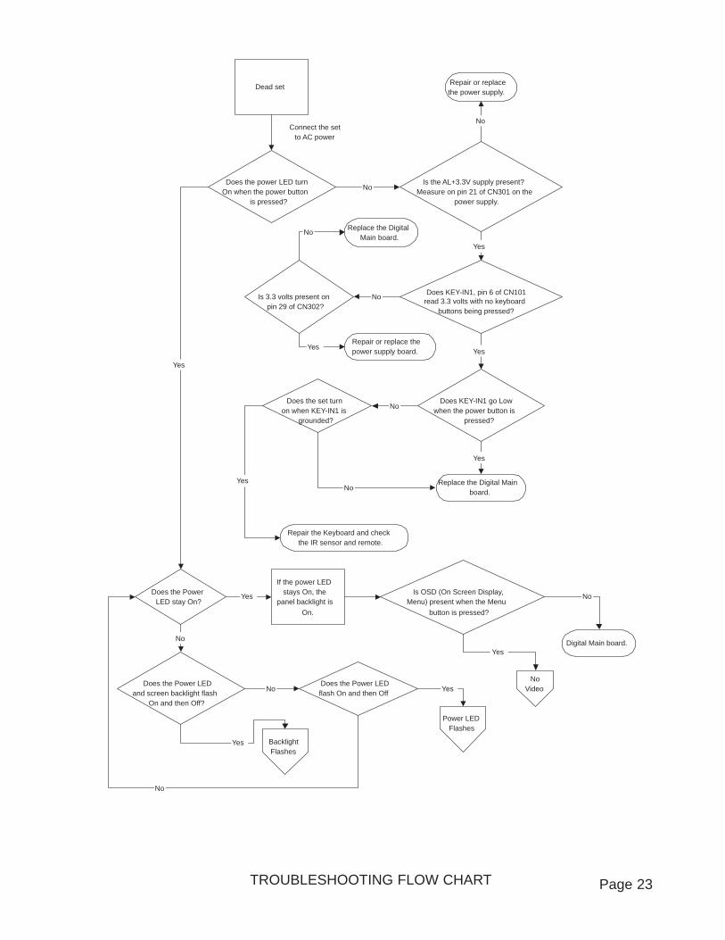
Dead set
Does the power LED turnOn when the power button
is pressed?
Is the AL+3.3V supply present?Measure on pin 21 of CN301 on the
power supply.
No
Repair or replacethe power supply.
Connect the setto AC power
No
Does KEY-IN1 go Lowwhen the power button is
pressed?
Does KEY-IN1, pin 6 of CN101 read 3.3 volts with no keyboard
buttons being pressed?
Yes
Is 3.3 volts present onpin 29 of CN302?
No
Repair or replace thepower supply board.Yes
Replace the DigitalMain board.
No
Yes
Replace the Digital Mainboard.
Yes
Does the set turn on when KEY-IN1 is
grounded?
No
No
Repair the Keyboard and checkthe IR sensor and remote.
Yes
Yes
Does the PowerLED stay On?
If the power LEDstays On, the
panel backlight isOn.
Yes Is OSD (On Screen Display,Menu) present when the Menu
button is pressed?
NoVideo
YesDigital Main board.
No
Does the Power LEDand screen backlight flash
On and then Off?
No
Does the Power LEDflash On and then OffNo
Power LEDFlashes
Yes
BacklightFlashes
Yes
No
Page 23TROUBLESHOOTING FLOW CHART
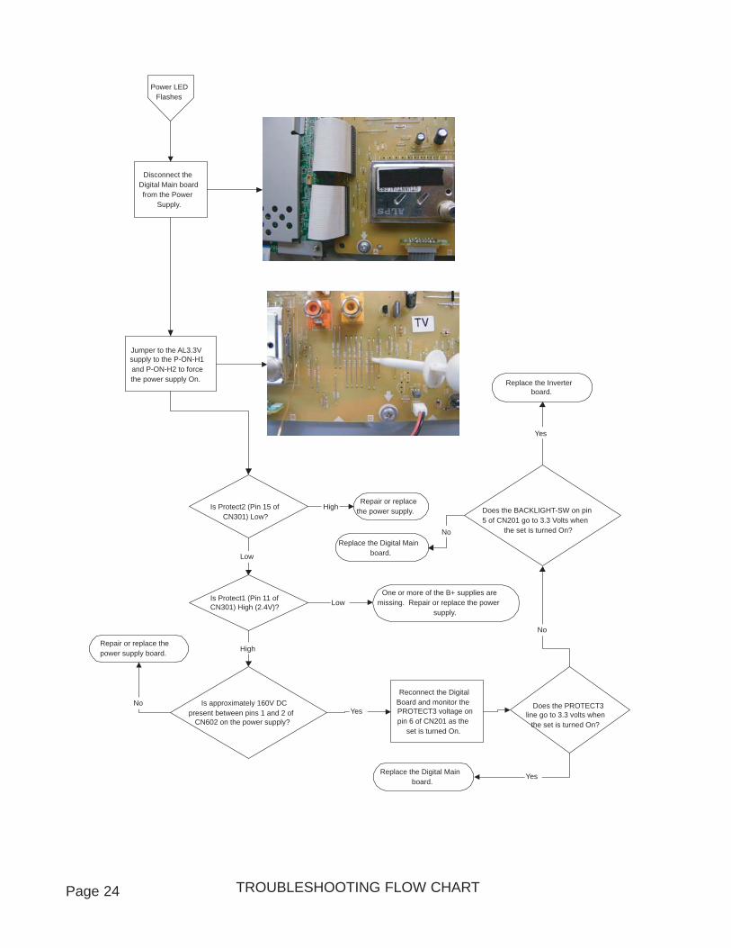
Power LEDFlashes
Disconnect theDigital Main boardfrom the Power
Supply.
Jumper to the AL3.3Vsupply to the P-ON-H1and P-ON-H2 to forcethe power supply On.
Is Protect2 (Pin 15 ofCN301) Low?
Repair or replacethe power supply.High
Is Protect1 (Pin 11 ofCN301) High (2.4V)?
Low
One or more of the B+ supplies aremissing. Repair or replace the power
supply.Low
High
Is approximately 160V DCpresent between pins 1 and 2 of
CN602 on the power supply?
Reconnect the DigitalBoard and monitor thePROTECT3 voltage onpin 6 of CN201 as the
set is turned On.
Yes
Repair or replace thepower supply board.
No Does the PROTECT3 line go to 3.3 volts when
the set is turned On?
Does the BACKLIGHT-SW on pin5 of CN201 go to 3.3 Volts when
the set is turned On?
No
Replace the Digital Mainboard.
Yes
Replace the Inverterboard.
Yes
Replace the Digital Mainboard.
No
Page 24 TROUBLESHOOTING FLOW CHART
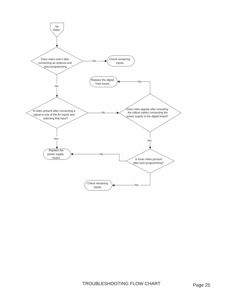
NoVideo
Is video present after connecting asignal to one of the AV inputs and
selecting that input?
Does video appear after reseatingthe ribbon cables connecting the
power supply to the digital board?No
Replace thepower supply
board.
Yes
Is tuner video presentafter auto-programming?
Replace the digitalmain board.
No
Yes
No
Check remaininginputs.
Yes
Does video return afterconnecting an antenna and
auto-programming.
No
Check remaininginputs.
Yes
Page 25TROUBLESHOOTING FLOW CHART
BacklightFlashes
Turn the set On while monitoring theHV output from the Inverter board at
each output one at a time.Repeat for each of the five locations.It is only necessary to place the scopeprobe in the proximity of the output as
shown at the right.If you connect directly, use a X100
probe.
The waveform willappear as shownto the right if the
output is working.
Is outputpresent at
each location?
The panel is most likely defective.Check panel connections to make sure
they are sucure.
Yes
Replace theInverter board.
No
Page 26 TROUBLESHOOTING FLOW CHART
NoAudio
Is audio presenton pins 6 and 8 of
CN301?
Turn the volumeup.
Change the Digital Mainboard.
No
Is the audio mute on pin 20 of CN302zero volts. (<0.4V)
Yes
Change the DigitalMain board.
No
Change the powersupply board.
Yes
Page 27TROUBLESHOOTING FLOW CHART
Abbreviation list
Description
1080i 1080 visible lines, interlaced1080p 1080 visible lines, progressive scan480i 480 visible lines, interlaced480p 480 visible lines, progressive scanADC A/D Analogue to Digital ConverterAFC Automatic Frequency Control: control signal used to tune to the correct
frequencyAGC Automatic Gain Control: algorithm that controls the video input of the
feature boxAM Amplitude ModulationAV Audio VideoC-FRONT Chrominance front inputCBA Circuit Board Assembly (or PWB)ComPair Computer aided rePairCSM Customer Service ModeCVBS Composite Video Blanking and SynchronizationCVBS-EXT CVBS signal from external source (VCR, VCD, etc.)CVBS-INT CVBS signal from TunerCVBS-MON CVBS monitor signalCVBS-TER-OUT CVBS terrestrial outDAC Digital to Analogue ConverterDFU Directions For Use: owner's manualDNR Dynamic Noise ReductionDRAM Dynamic RAMDSP Digital Signal ProcessingDTS Digital Theatre SoundDVD Digital Video DiscEEPROM Electrically Erasable and Programmable Read Only MemoryEPLD Electronic Programmable DeviceEXT EXTernal (source), entering the set by cinches (jacks)FBL Fast Blanking: DC signal accompanying RGB signalsFLASH FLASH memoryFM Field Memory / Frequency ModulationFMR FM RadioFRC Frame Rate ConverterFRONT-C Front input chrominance (SVHS)FRONT-DETECT Front input detectionFRONT-Y_CVBS Front input luminance or CVBS (SVHS)H H_sync to the module HD High DefinitionHDMI High Definition Multimedia Interface HP HeadPhone
Page 28
I2C Integrated IC busI2S Integrated IC Sound busIC Integrated CircuitIF Intermediate FrequencyInterlaced Scan mode where two fields are used to form one frame. Each field contains
half the number of the total amount of lines. The fields are written in 'pairs', causing line flicker.
IR Infra RedIRQ Interrupt ReQuestLast Status The settings last chosen by the customer and read and stored in RAM or in the
NVM. They are called at start-up of the set to configure it according the customers wishes.
LCD Liquid Crystal DisplayLED Light Emitting DiodeLINE-DRIVE Line drive signalLVDS Low Voltage Differential Signalling, data transmission system for high speed
and low EMI communication.MPEG Motion Pictures Experts GroupNVM Non Volatile Memory: IC containing TV related data (for example, options)OSD On Screen DisplayProgressive Scan Scan mode where all scan lines are displayed in one frame at the same
time, creating a double vertical resolution.RAM Random Access MemoryRC Remote Control transmitterRC5 Remote Control system 5, the signal from the remote control receiver RGB Red, Green, and Blue. The primary colour signals for TV. By mixing
levels of R, G, and B, all colors (Y/C) are reproduced.RGBHV Red, Green, Blue, Horizontal sync, and Vertical syncROM Read Only MemorySAM Service Alignment ModeSIF Sound Intermediate FrequencySC SandCastle: two-level pulse derived from sync signalsSCL CLock Signal on I2C busSDA DAta Signal on I2C busSDRAM Synchronous DRAMSIF Sound Intermediate FrequencySTBY STandBYVGA Video Graphics ArrayXTAL Quartz crystalYPbPr Component video (Y= Luminance, Pb/Pr= Colour difference signals)Y/C Luminance (Y) and Chrominance (C) signalY-OUT Luminance-signal
Page 29
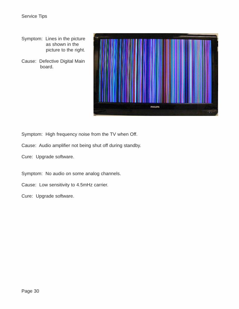
Service Tips
Symptom: Lines in the pictureas shown in the picture to the right.
Cause: Defective Digital Mainboard.
Symptom: High frequency noise from the TV when Off.
Cause: Audio amplifier not being shut off during standby.
Cure: Upgrade software.
Symptom: No audio on some analog channels.
Cause: Low sensitivity to 4.5mHz carrier.
Cure: Upgrade software.
Page 30


MM081909