by thiago rocha de assis - etd.library.vanderbilt.edu · iii to my wife, reginara and my parents,...
TRANSCRIPT
SOFT ERROR AWARE PHYSICAL SYNTHESIS
By
Thiago Rocha de Assis
Dissertation
Submitted to the Faculty of the
Graduate School of Vanderbilt University
in partial fulfillment of the requirements
for the degree of
DOCTOR OF PHILOSOPHY
in
Electrical Engineering
December, 2015
Nashville, Tennessee
Approved:
Bharat L. Bhuva, Ph.D.
Ronald D. Schrimpf, Ph.D.
William H. Robinson, Ph.D.
Aniruddha S. Gokhalé, Ph.D.
Shi-Jie Wen, Ph.D.

ii
Copyright © 2016 by Thiago Rocha de Assis
All Rights Reserved

iii
To my wife, Reginara and my parents, Ailton and Telma for their infinite support

iv
ACKNOWLEDGEMENTS
This work would not have been possible without a combination of both institutional support and the
guidance of great mentors. I would like to thanks my advisor, Dr. Bharat L. Bhuva for his unconditional
support for my research, and guidance trough graduate school. I also would like to thanks Dr. Ronald D.
Schrimpf, for his guidance over this research, providing key insights that has allowed the conclusion of
this work.
I also would like to thanks the professors from the Radiation Effects and Reliability Group for their
feedback over this research, usually provided during group meetings. To the student members of the
Radiation Effects and Reliability group, I would like to thank you all for the friendship and great
moments at school.
From the Industry, I would like to thanks Dr. Shi-Jie Wen from Cisco Systems for his professional
guidance through my internships at Cisco. Those discussions had a key impact over the goals of this
research. I also thanks, Cisco Systems for the internship opportunities.
From the Universidade Federal do Rio Grande do Sul (UFRGS), I would like to thanks Dr. Ricardo Augusto
da Luz Reis, for his inspiration and contribution to the Electronic Design Automation algorithms that
have impacted this work. The Physical Synthesis flow developed in this thesis was deeply inspired by the
work done by the EDA research group from UFRGS. Thanks also for my old colleagues from UFRGS that
were available to provide important guidance trough the development of the EDA algorithms used in
this research.
Last, but not less important, I would like to thanks the Vanderbilt University, the SER Consortium and the Defense Threat Reduction Agency (DTRA), for providing the funding that made this work possible. The resources provided by these institutions were key to allow the proper execution of this Ph.D. thesis.

v
TABLE OF CONTENTS
DEDICATION ................................................................................................................................................. iii
ACKNOWLEDGEMENTS ................................................................................................................................ iv
LIST OF TABLES ............................................................................................................................................ vii
LIST OF FIGURES ......................................................................................................................................... viii
Chapter
1. Introduction .............................................................................................................................................. 1
1.1 Related Work ...................................................................................................................................... 3
1.2 Contribution ........................................................................................................................................ 5
1.3 Organization ........................................................................................................................................ 6
2. Radiation Effects – Soft Errors and Mechanisms ...................................................................................... 7
2.1 Soft Error Mechanism ......................................................................................................................... 8
2.1.1 Well Debiasing and Parasitic Bipolar Amplification ................................................................. 10
2.2 Radiation Event Modeling ................................................................................................................. 13
3. Collected Charge Modeling ..................................................................................................................... 16
3.1 Background ....................................................................................................................................... 16
3.2 ADC Model and Proposed Extension ................................................................................................ 17
3.3. Devices, Technology Nodes and Radiation Event ............................................................................ 21
3.4. Pre-Characterization – Omega ......................................................................................................... 23
3.5 Single Node Collected Charge ........................................................................................................... 26
3.6. Error Comparison between ADC, RPP and IRPP............................................................................... 29
3.7 Charge Sharing .................................................................................................................................. 31
3.8 Conclusions ....................................................................................................................................... 33
4. Single Event Transient and Soft Error Cross-Section Modeling .............................................................. 34
4.1 SET Pulse Width Model ..................................................................................................................... 35
4.1.1 Models and Operation Condition ............................................................................................ 41
4.1.2 SET Pulse Width Results ........................................................................................................... 41
4.1.3 SET Pulse Width Model Conclusions........................................................................................ 47
4.2 Circuit De-rating Factors ................................................................................................................... 47
4.3 Soft Error Sensitivity and Cross Section Estimation .......................................................................... 51
vi
4.4 Circuit Analysis Conclusions .............................................................................................................. 56
5. Physical Synthesis ................................................................................................................................... 57
5.1 Physical Synthesis Flow ..................................................................................................................... 59
5.2 Electrical Correction Techniques and Soft Errors ............................................................................. 61
5.3 Automatic Placement ........................................................................................................................ 64
5.4 Simulated Annealing Placement ....................................................................................................... 66
5.5 Quadratic Placement ........................................................................................................................ 68
5.5.1 Global Placement ..................................................................................................................... 69
5.5.2 Detailed Placement .................................................................................................................. 71
5.6 Time Analysis..................................................................................................................................... 75
5.7 Electrical Correction & Legalization .................................................................................................. 79
5.8 Simulated Annealing vs Quadratic Programming Placement ........................................................... 80
5.9 Conclusions ....................................................................................................................................... 82
6. Soft Error Aware Physical Synthesis ........................................................................................................ 83
6.1 Framework – Data Visualization ....................................................................................................... 84
6.2 Electrical Correction Techniques Soft Error Cross-Section ............................................................... 89
6.3 Gate Sizing and Cloning for Hardening Soft Error Cross-Section ...................................................... 93
6.4 Tap Cell Placement Aware of Soft Errors .......................................................................................... 95
6.5 Conclusions ..................................................................................................................................... 100
7. Conclusions ........................................................................................................................................... 101
REFERENCES .............................................................................................................................................. 103
Open Cell Library and Benchmarks ........................................................................................................... 111
A.1 Open Cell Library ............................................................................................................................ 111
A.2 Benchmarks .................................................................................................................................... 114
List of Publications .................................................................................................................................... 115
Industry Awards\Competitions ................................................................................................................. 116
vii
LIST OF TABLES
Table Page
1-1 Summary of main characteristics of related work ................................................................................ 4
3-1 Technology Parameters ...................................................................................................................... 22
4-1 Circuit and operation condition parameters ...................................................................................... 41
4-2 Model vs experimental data for 65nm inverters ................................................................................ 47
5-1 Comparison between placement algorithms [39] .............................................................................. 65
5-2 Simulated Annealing vs Quadratic Programming .............................................................................. 81
6-1 Electrical correction techniques impact to the circuit area ................................................................ 90
6-2 Radiation hardening techniques impact to the circuit area ............................................................... 93
6-3 Impact of tap placement algorithms to the HPWL ............................................................................. 97
A-1 The full cycle delay of standard cells, over different load capacitances. Delay provided in ns. ...... 112
A-2 Metallization characteristics ............................................................................................................. 112
A-3 Flip Flop Technology Information ..................................................................................................... 113
A-4 OCL Cells used by the benchmarks ................................................................................................... 113
viii
LIST OF FIGURES
Figure Page
2-1 Electric field funneling in a junction during radiation event [16] ......................................................... 8
2-2 Current generated by the SEE [16] ....................................................................................................... 9
2-3 Parasitic bipolar amplification [17] ..................................................................................................... 10
2-4 Resistances associated with the well potential [17]. .......................................................................... 11
2-5 (a) Detector hit by a 67 MeV positive muon (mµ+). Blue and green lines indicate the path of positive
and neutral charge respectively. (b) Energy distribution in the detector. ................................................. 14
3-1 Different regions formed after the transit of an ion through a p-n junction [33]. ............................. 18
3-2 Omega Function as a function of depth. Filled circles represent TCAD results, dotted line is for the
Omega function. ......................................................................................................................................... 24
3-3 Collected Charge vs Depth for the 130 nm technology node parameters listed in Table I. ............... 25
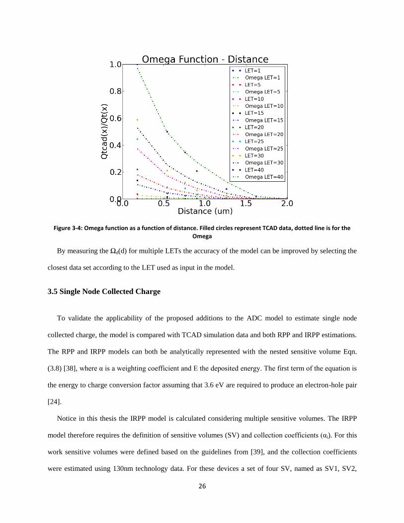
3-4 Omega function as a function of distance. Filled circles represent TCAD data, dotted line is for the
Omega ......................................................................................................................................................... 26
3-5 Simulation results for Collected Charge for proposed ADC model and TCAD data in the literature
show excellent agreement for all technology nodes considered in this work. .......................................... 28
3-6 Mean and standard deviation for error in estimating the collected charge for the proposed ADC
model, RPP model, and IRPP model when compared to TCAD results. ..................................................... 29
3-7 Normalized mean error of RPP and IRPP related to the ADC ............................................................. 30
3-8 Collected Charge due to charge-sharing as a function of distance from the hit location for a 40 nm
node. TCAD data from the literature for a particle with (a) LET equal to 1 MeV/mg/cm2, and, (b) LET
equal to 10 MeV/mg/cm2, (c) LET equal to 30 MeV/mg/cm2 ................................................................... 32
4-1 The SET pulse width generated by a Soft Error, measured at half VDD. ............................................ 34
4-2 Circuit effects influencing cell response during an SEE ...................................................................... 36
4-3 Circuits used for the technology characterization .............................................................................. 36
4-4 Restoring current factor for transistors in series ................................................................................ 37
4-5 Restoring current factor for transistors in parallel ............................................................................. 38
4-6 Load Capacitance Factor ..................................................................................................................... 39
4-7 OAI21_X1 Cell on-state resistance modeling ...................................................................................... 40
4-8 SET Pulse width from 130nm standard cells comparison between model and spice ........................ 42
4-9 SET pulse width comparison for 90, 65 and 40nm technology nodes. ............................................... 45
4-10 Spice benchmark used to evaluate the SET pulse quenching. .......................................................... 46
4-11 SET Pulse Quenching ......................................................................................................................... 46
4-12 - De rating probabilities. Electrical, Logical and Timing DR respectively. ........................................... 48
4-13 Logical Derating Calculation [48] ...................................................................................................... 50
4-14 NAND gate logic state probability ..................................................................................................... 50
4-15 Error probability matrix of the SEUTOOL [49]. ................................................................................. 53
4-16 Test Chip vs Model Cross Section - 4 Bit comparator ....................................................................... 55
4-17 Test Chip vs Model Cross Section - 72 Inverter chain ....................................................................... 56
5-1 Typical EDA flow [51] .......................................................................................................................... 57
5-2 Netlist and its circuit representation [53] ........................................................................................... 58
ix
5-3 Physical Synthesis output [53] ............................................................................................................ 59
5-4 Physical Synthesis based on a commercial design flow [54] .............................................................. 60
5-5 Gate Sizing technique ......................................................................................................................... 62
5-6 - Gate Cloning technique ...................................................................................................................... 62
5-7 Gate Cloning for Hardening ................................................................................................................ 63
5-8 Buffering the interconnectivity ........................................................................................................... 63
5-9 Gate Relocation (Cell swap) ................................................................................................................ 64
5-10 Simulated Annealing Pseudocode [66] ............................................................................................. 67
5-11 Developed placement flow ............................................................................................................... 68
5-12 Placement Local Reordering ............................................................................................................. 73
5-13 Vertical cell swap .............................................................................................................................. 74
5-14 Horizontal Cell Swap ......................................................................................................................... 74
5-15 RC delay network used to model the interconnectivity [76] ............................................................ 75
5-16 Line-to-Ground capacitance – Interconnection line facing the substrate [78] ................................. 76
5-17 Snapshot of part of the RC network used in simulations ................................................................. 77
5-18 Elmore model vs simulation .............................................................................................................. 78
5-19 Total post placement circuit wire length of Simulated Annealing vs Quadratic Programming
Placement ................................................................................................................................................... 81
5-20 Total placement execution run time of Simulated Annealing vs Quadratic Programming Placement
.................................................................................................................................................................... 82
6-1 Soft Error Aware Physical Synthesis Flow ........................................................................................... 84
6-2 Placed Netlist- ISCAS C880 .................................................................................................................. 86
6-3 Netlist Logical De-rating ...................................................................................................................... 87
6-4 Netlist Minimum Propagation delay ................................................................................................... 88
6-5 Netlist SET Pulse width........................................................................................................................ 89
6-6 Electrical Correction – Gate Sizing – LET= 5.5 MeV*cm2/mg and 14 MeV*cm2/mg .......................... 91
6-7 Electrical Correction – Gate Clone – LET= 5.5 MeV*cm2/mg and 14 MeV*cm2/mg .......................... 91
6-8 Electrical Correction – Buffering – LET= 5.5 MeV*cm2/mg and 14 MeV*cm2/mg ............................. 92
6-9 Electrical Correction – LET= 5.5 MeV*cm2/mg and 14 MeV*cm2/mg ................................................ 92
6-10 Hardening techniques Soft error cross-section - 5.5 MeV*cm2/mg ................................................. 94
6-11 Hardening techniques Soft error cross-section -14 MeV*cm2/mg ................................................... 95
6-12 Soft-error cross-section comparison between cells with tap and tap less cells – 5.5 MeV*cm2/mg. 96
6-13 Standard Tap Placement vs Hardening Tap Placement C1355 ......................................................... 97
6-14 Standard Tap Placement vs Hardening Tap Placement 5 MeV*cm2/mg .......................................... 98
6-15 Standard Tap Placement vs Hardening Tap Placement 14 MeV*cm2/mg ........................................ 98
6-16 SET pulse width distribution – C880 - (a) LET=5.5 MeV*cm2/mg. (b) LET=14 MeV*cm2/mg. .......... 99
6-17 SET pulse width distribution – C1355 - (a) LET=5.5 MeV*cm2/mg. (b) LET=14 MeV*cm2/mg. ........ 99
6-18 SET pulse width – c880 – Standard Tap vs Tap Hardening ............................................................. 100
A-1 INV_X1 Standard Cell - OCL 45nm [81] ............................................................................................. 111
A-2 ISCAS'85 Benchmark details [83] ...................................................................................................... 114
1
CHAPTER 1
1. Introduction
Soft errors are events generated by the interaction of alpha particles, neutrons, protons, electrons,
muons, or heavy ions with semiconductor regions in an Integrated Circuit (IC), potentially causing errors
[1]. The growing concern of the semiconductor industry related to Soft Errors is attributed to the
increased sensitivity of electronic devices occasioned by “Moore’s Law Scaling”. With the scaling of
planar technologies from micrometer scale towards current nanometer scale transistors, parameters, such
as transistors sizes, nodal capacitances, and interconnectivity resistances have decreased to the level
where they directly impact the technology node sensitivity to radiation [2].
As charged particle transverses through a semiconductor region, it loses energy through coulombic
interactions and generates electron-hole pairs. The effect of such charge generation inside a
semiconductor region will be a function of both characteristics of the radiation event and physical details
of the semiconductor region. The understanding of the detailed characteristics of the radiation event has
an important role in the circuit soft error characterization. As it was shown by [3], ions with the same
energy but different Linear Energy Transfer (LET) values have significantly different cross section.
Moreover, ion-to-ion interaction, which can be predicted by Monte Carlo methods, can also impact the
device error cross section.
In the context of transistors, the semiconductor technology process parameters and operational
conditions have strong influence in how charge is collected by the individual transistors. As discussed by
[1], lower operating bias, reduced switching energy, substrate doping and device cross-section have
directly impacted on circuits soft error rate. The increase in transistor density on a die is also causing new
2
error modes and mechanisms. With the technology node scaling, more transistors can be fabricated in a
given semiconductor region, allowing multiple transistors to collect charge from a single radiation strike,
a phenomenon referred to as charge sharing [4]. This is an important issue that has been a focus of the
research community for a long time, and is discussed in more details later.
In parallel to the increasing concern for Soft Errors in the reliability field, the Electronic Design
Automation (EDA) research field has gained great attention from research community and industry. EDA
has emerged as key science to allow the design of nanometer-size transistors and the integration of
billions of electronic components in a single IC. Some of the reasons for the rapid growth and evolution
of the EDA field were the increasing complexity of new technologies, extremely high density transistors
in a single IC, and concerns over circuit designers productivity [5].
What is important to understand at this moment is that EDA has become a key part of the
semiconductor industry to support the deployment of current and future semiconductor technologies.
EDA allows the increasing complexity of new technologies to be hidden from semiconductor design
engineers, with algorithms making key decisions that impact the electrical characteristics of a circuit.
Without EDA tools, the latest generation of IC designs with billions of transistors [6] could not be
possible. In current nanometer technology nodes it is impractical to consider a commercial design process
without any kind of EDA tools to assist circuit designers.
EDA can be defined as a collection of methodologies, algorithms and metrics that automate the design,
verification and test of electronic components [5]. This Ph.D. thesis is focused on design automation,
more specifically the Physical Synthesis process. For the moment, it’s enough to understand that Physical
Synthesis is the process responsible for converting a list of logical gates and macro blocks into a physical
representation of the IC that is placed, routed and electrically correct. The Physical Synthesis is one of the
last steps of the Application Specific Integrated Circuit (ASIC) design flow process, before masks are
built and sent to the IC foundries.
The case for the analysis of Soft Errors during the Physical Synthesis arises due to both cell placement
and electrical correction techniques influencing the electrical characteristics of the circuit. Moreover,

3
because of the increase in the transistor density, charge sharing has become an issue and the relationship
between adjacent electrical components impacts the overall circuit sensitivity to soft errors. The report [5]
from the National Science Foundation (NSF), 2006, indicates soft error analysis as one of the key metrics
to be integrated into the EDA flow.
Another important aspect is the commercial impact of the Physical Synthesis to the EDA industry. The
Physical Synthesis by itself is responsible for most revenue by the EDA Industry, accounting for
hundreds of millions of dollars [7]. On the other side, for companies, Non-Recurring Engineering (NRE)
costs of Very Large Scale Integration (VLSI) designs are skyrocketing, and it has become critical for
companies to avoid any kind of redesign effort. The report [5] from 2006, estimates an NRE of about
$30M/IC design for VLSI designs.
The integration of Soft Error awareness into the Physical Synthesis could potentially be used by
companies to avoid redesign efforts in situations where Soft Error susceptibility needs to be reduced.
Performing the soft error analysis automatically in the synthesis flow will be necessary due to the
multitude of parameters affecting the physical synthesis and soft errors. It’s the goal of this research to
identify metrics for the soft error characterization and to investigate Physical Synthesis transformations
that impact the soft error cross-section.
1.1 Related Work
The work published by [8, 9] implements a Placement aware of Soft Errors, using a Simulated
Annealing algorithm, and later using Quadratic Modeling for the objective function optimization. These
works use current waveforms to evaluate the circuit node soft-error sensitivity and propose the selective
increase in the wire length, to increase the interconnection Resistance-Capacitance (RC), thus leading to
the reduction of soft errors. Results from these papers indicate an average 27.12% [8] and 47.01% [9] soft
error rate reduction according to their metric.

4
There are several differences between the work proposed by [8, 9] and the one proposed in this thesis.
A key difference is that the selective wire length increase is not the objective constraint proposed in this
work. Wire length increase is associated with both delay and power consumption increase, two objectives
that are usually minimized by standard placement flows [7]. Another important difference is that the
primary goal of this thesis is not to propose hardening techniques, but to present a detailed modeling
approach to allow the integration of soft error analysis into the synthesis flow.
Other researchers have directed their effort to use commercial placement tools for Soft Error reduction
[10, 11]. These projects usually refer to this methodology as a “Constrained Placement” where the jobs
submitted to commercial placement tools receive additional constraints, usually used to group cells. Both
the projects try to enhance the “Pulse Quenching” [12] effect by grouping cells into macros. Results from
these papers indicate an average 35% [10] and 9-19% [11] soft error rate reduction. Table 1 is used to
summarize the main aspects of the papers discussed above.
Table 1-1: Summary of main characteristics of related work
Constraint Objective Soft Error Reduction
Placement Algorithm
[8, 9]
Wire length Increase interconnect RC 27.12%, 47.01%
Constrain Placement
Tool [11, 10]
Cell grouping Increase charge sharing 35%, 9-19%
According to the metrics used by the papers referenced before, the use of the RC product to filter small
SETs is able to achieve a soft error reduction in the range of 27-47%, and for placements enhancing SET
Pulse Quenching, the sensitivity reduction is in the range of 9-35%. All of these papers assume a very
simple model for radiation events based on a simplistic double-exponential hit-current model. Though
such a model is good enough for approximate analysis, pulse-quenching effects require a precise hit-
current model in space and time to accurately model effects of an ion hit.

5
1.2 Contribution
The primary goal of this work is to build a methodology capable of properly modeling the Soft Error
event, starting with the interaction of particles with the semiconductor region to the circuit-level response.
Detailed characteristics of the radiation event are embedded in the methodology, to allow the proper
characterization of the circuit cross-section and the evaluation of the influence of both electrical
correction and circuit hardening techniques to the cross-section. Such accurate cross-section modeling
efforts will result in better physical synthesis flow. Individual contributions are:
1. Develop a methodology for soft error analysis in a computationally intensive process.
a. Develop analytical models to estimate Collected Charge and Charge Sharing effects
given a particle energy deposition profile and technology node characteristics.
b. Develop a methodology to estimate the SET Pulse Width.
c. Develop a methodology to estimate the soft-error cross-section.
2. Evaluate the impact of electrical correction techniques to the soft-error cross-section.
a. Gate Sizing, Gate Cloning and Buffering
3. Propose the optimization of Tap Cell placement to reduce the soft-error cross-section.
The results of this work will allow a better understanding by the EDA community of how the Physical
Synthesis impacts the circuit-level soft-error cross-section and the limitations of various hardening
techniques. By integrating this analysis into the Physical Synthesis flow, semiconductor companies will
be able to reduce the soft -error cross-section of circuits without the need of a re-design.

6
1.3 Organization
This dissertation is organized as follow:
Chapter 2: A background review of soft errors is discussed. Mechanisms involved in the
charge collection by a diode and the parasitic bipolar amplification are discussed.
Chapter 3: The model to estimate the collected charge and charge sharing by both p-type
and n-type transistors is discussed, and a comparison with other models is presented.
Chapter 4: The SET pulse width estimation methodology is discussed, presenting results
from several different technology nodes. The methodology to estimate the circuit soft error
cross-section is discussed.
Chapter 5: The state of the art in of Physical Synthesis process is summarized, along with
methods and transformations that lead to electrical changes that can impact circuit sensitivity to
radiation. A discussion over the ideal synthesis steps to integrate the soft error analysis is
presented.
Chapter 6: The impact of the electrical correction techniques: Gate Sizing, Gate Cloning
and Buffering are discussed and their impact to the circuit soft-error cross-section is evaluated
Circuit hardening based on Gate Sizing, Cloning and Tap Cell Placement techniques are
evaluated.
Chapter 7: Main thesis conclusions are discussed.
7
CHAPTER 2
2. Radiation Effects – Soft Errors and Mechanisms
Soft errors are transient events generated by the interaction of radiation with the semiconductor
regions. These errors are considered transient because they will eventually disappear with circuit
operation and do not directly cause permanent damage. There is an extensive range of error modes
characterized as permanent, but these are not the focus of this work. For a broader perspective over
permanent errors caused by radiation, please consult references [13, 14].
At this moment, it is important to identify the nomenclature used by the community to classify error
modes associated with soft errors in digital circuits. The following are the error modes described by the
research community that are important to the understanding of this work:
Single-Event Transient (SET): The term SET is used to refer to a voltage transient that is
generated in a logic gate, usually in a combinational logic block, and is able to propagate
through the circuit [1].
Single-Event Upset (SEU): An SEU refers to a soft error in a sequential element (memory).
The SEU is able to flip the logic state stored in the feedback loop of the memory element [1].
Multiple Bit Upset (MBU), Multiple Event Transients (MET): Both MBU and MET refers to
multiple combinational and sequential elements been affected by a single event [1].
As this research focuses on the Physical Synthesis process, the primary error modes of interest are the
SET/MET events. The SEU/MBU error modes are not ignored, but as memory elements are pre-designed
and included in the IC as Standard Cells, the Physical Synthesis will have little impact on the soft error
performance of memory cells. The next sections summarize the fundamentals of the soft error
phenomena, followed by the procedure used to model the radiation event in this work, and the

8
methodologies used to characterize both the semiconductor device and circuit netlist response to Single
Event Effects (SEE).
2.1 Soft Error Mechanism
The main physical mechanisms involved in the soft error event are shown in figure 2-1. In the figure
an n-p diode representing a transistor drain, during a radiation event is shown. The particle can transfer
energy by direct ionization (coulomb interaction) or indirect ionization (nuclear reaction). Direct
ionization will transfer energy to the semiconductor material, exciting electrons from the valence band to
the conduction band, thus generating electron hole pairs (e-h pairs). Indirect ionization will occur if a
particle, such as a neutron or a proton, strikes an atom in the lattice structure, thus generating secondary
ions. These ions create e-h pairs through direct ionization.
In the event shown in Figure 2.1, the generated e-h pairs create a distortion of the electric field located
in the depletion region boundary (charged region). The distortion of the electric field will extend the
collection area of the region, thus increasing the collected charge [15]. Carriers will move towards the
depletion region by drift due to the presence of an electric field and diffusion due to the gradient of
carriers in the region.
Figure 2-1 Electric field funneling in a junction during radiation event [16]
9
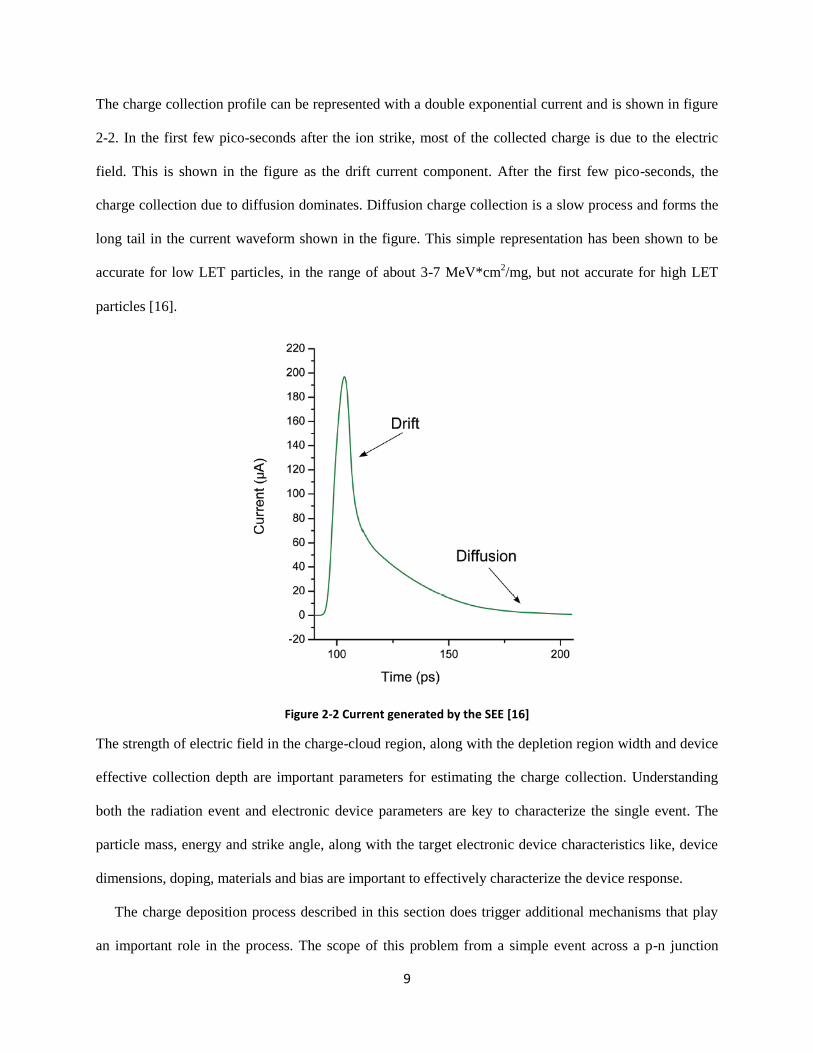
The charge collection profile can be represented with a double exponential current and is shown in figure
2-2. In the first few pico-seconds after the ion strike, most of the collected charge is due to the electric
field. This is shown in the figure as the drift current component. After the first few pico-seconds, the
charge collection due to diffusion dominates. Diffusion charge collection is a slow process and forms the
long tail in the current waveform shown in the figure. This simple representation has been shown to be
accurate for low LET particles, in the range of about 3-7 MeV*cm2/mg, but not accurate for high LET
particles [16].
Figure 2-2 Current generated by the SEE [16]
The strength of electric field in the charge-cloud region, along with the depletion region width and device
effective collection depth are important parameters for estimating the charge collection. Understanding
both the radiation event and electronic device parameters are key to characterize the single event. The
particle mass, energy and strike angle, along with the target electronic device characteristics like, device
dimensions, doping, materials and bias are important to effectively characterize the device response.
The charge deposition process described in this section does trigger additional mechanisms that play
an important role in the process. The scope of this problem from a simple event across a p-n junction
10
event has to be expanded to take into account effects of parasitic elements, multiple transistors, and
standard cells. The well de-biasing and the parasitic bipolar amplification are going to be discussed next.
2.1.1 Well Debiasing and Parasitic Bipolar Amplification
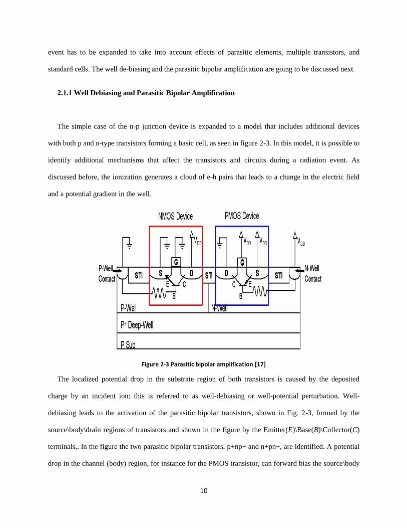
The simple case of the n-p junction device is expanded to a model that includes additional devices
with both p and n-type transistors forming a basic cell, as seen in figure 2-3. In this model, it is possible to
identify additional mechanisms that affect the transistors and circuits during a radiation event. As
discussed before, the ionization generates a cloud of e-h pairs that leads to a change in the electric field
and a potential gradient in the well.
Figure 2-3 Parasitic bipolar amplification [17]
The localized potential drop in the substrate region of both transistors is caused by the deposited
charge by an incident ion; this is referred to as well-debiasing or well-potential perturbation. Well-
debiasing leads to the activation of the parasitic bipolar transistors, shown in Fig. 2-3, formed by the
source\body\drain regions of transistors and shown in the figure by the Emitter(E)\Base(B)\Collector(C)
terminals,. In the figure the two parasitic bipolar transistors, p+np+ and n+pn+, are identified. A potential
drop in the channel (body) region, for instance for the PMOS transistor, can forward bias the source\body
11
junction leading to the activation of the parasitic bipolar transistor [17]. In this process carriers are going
to be injected from the emitter to the body, and collected by the collector terminal, thus increasing the
total amount of charge collected by the drain region during the radiation event. This charge, will them be
represented at the circuit-level as a transient current.
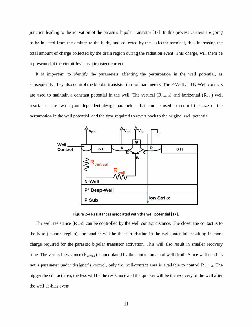
It is important to identify the parameters affecting the perturbation in the well potential, as
subsequently, they also control the bipolar transistor turn-on parameters. The P-Well and N-Well contacts
are used to maintain a constant potential in the well. The vertical (Rvertical) and horizontal (Rwell) well
resistances are two layout dependent design parameters that can be used to control the size of the
perturbation in the well potential, and the time required to revert back to the original well potential.
Figure 2-4 Resistances associated with the well potential [17].
The well resistance (Rwell), can be controlled by the well contact distance. The closer the contact is to
the base (channel region), the smaller will be the perturbation in the well potential, resulting in more
charge required for the parasitic bipolar transistor activation. This will also result in smaller recovery
time. The vertical resistance (Rvertical) is modulated by the contact area and well depth. Since well depth is
not a parameter under designer’s control, only the well-contact area is available to control Rvertical. The
bigger the contact area, the less will be the resistance and the quicker will be the recovery of the well after
the well de-bias event.
12
In dual well technology process with n-well, the p-channel transistor is considered to be less tolerant to
the well-debias when compared with the n-channel transistor [18], due to both the fact that holes have
lower mobility when compared to electrons and the confinement of charge in the well structure. For an
additional insight related to well engineering techniques that can be used to reduce the well de-bias,
please consult reference [19].
Now that a basic understanding of how the well de-bias can result in more charge collection by
semiconductor regions, it’s time to consider the Charge Sharing event. It turns out that in real circuits,
several transistors are placed in close proximity of each other, sharing the same well. With scaling, the
distances between these transistors are becoming increasingly smaller, and the transistor density is
increasing. On the top of that, to increase the density of transistors, the number of well contacts in the IC
is reduced. At advanced technology nodes, well and substrate contacts are designed as a separate cell and
placed at a distance dictated by Design rules. Standard cells that do not contain well/substrate contacts are
referred as tap less cells, and the cell containing the well/substrate contact is referred as Well Tap cell or
Tap cell. These design practices leads to increased sensitivity of transistors to the well de-bias effects.
Due to the proximity of the transistors, charge sharing has become a reality. In nanometer technology
nodes, a single radiation event can cause multiple logical nodes to collect charge, resulting in possible
Multiple Event Transients (MET) propagating through the circuit. The charge-sharing event was
investigated by [20, 21] in 130-nm and 90-nm technologies to show how it affects single-event sensitivity
and hardening techniques for these and future technologies. Charge sharing may also be enhanced when a
particle incident at a sharp angle traverses through multiple transistors.
With the understanding of important physical mechanisms required to model the transistor/circuit
response during a radiation event, the next step will be to develop computationally efficient models for
soft error analysis in this thesis. To achieve this goal, first the collected charge by a node needs to be
estimated, followed by transformation of the collected charge into an electrical pulse at each of the node
being affected. Simply put, we need to estimate the charge collection at all affected nodes and then
convert the collected charge into multiple SET pulses in the circuit. The next section will discuss how the

13
radiation event is modeled, followed by the charge collection and supporting models to estimate standard
cell response.
2.2 Radiation Event Modeling
Modeling the radiation event is a challenging process, due to its complexity. One of the main problems
associated with the characterization of the radiation event is the fact that the radiation environment plays
an important role in the characteristics of particles involved in the process. As it was discussed before, the
radiation event can be classified between direct and indirect ionization, this in turns leads to the fact that
different radiation environments can have different prevalent mechanisms to generate SEE. Discussing
the different radiation environments and details over direct and indirect ionization are not the objective of
this thesis, consult reference [3] for a better understanding of radiation environment characterization.
What is important to understand at this moment is that direct ionization can be directly described by
the Linear Energy Transfer (LET), but not indirect ionization. To make the situation more complicated, in
the terrestrial environment indirect ionization by neutrons play a major role in the characterization of the
single-event effects. Modeling the radiation event in a way that allows both direct and indirect ionization
to be integrated into the design/simulation flow is key for the soft error analysis.
A solution to bypass this problem is to use external tools and frameworks to characterize the event and
model both direct and indirect ionization as a profile of energy deposition. This profile can be extracted
using Monte Carlo simulation tools, like SRIM 2008 [22] and the Geant4 framework [23]. These
simulators allow the description of the target material along with characteristics of the radiation particle in
detail, and have been used before for this purpose. In figure 2-5, images from a Geant4 application
developed to estimate the range and the energy deposition profile of positive and negative muons in a
muon detector are shown.
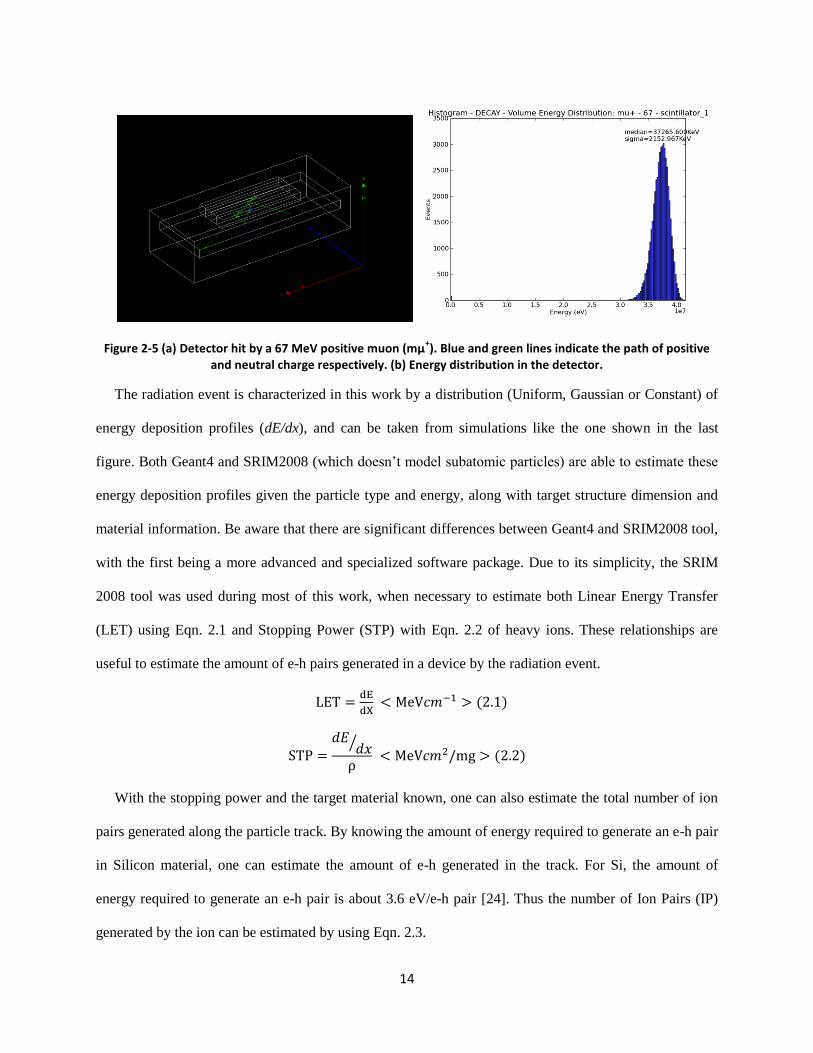
14
Figure 2-5 (a) Detector hit by a 67 MeV positive muon (mµ+). Blue and green lines indicate the path of positive
and neutral charge respectively. (b) Energy distribution in the detector.
The radiation event is characterized in this work by a distribution (Uniform, Gaussian or Constant) of
energy deposition profiles (dE/dx), and can be taken from simulations like the one shown in the last
figure. Both Geant4 and SRIM2008 (which doesn’t model subatomic particles) are able to estimate these
energy deposition profiles given the particle type and energy, along with target structure dimension and
material information. Be aware that there are significant differences between Geant4 and SRIM2008 tool,
with the first being a more advanced and specialized software package. Due to its simplicity, the SRIM
2008 tool was used during most of this work, when necessary to estimate both Linear Energy Transfer
(LET) using Eqn. 2.1 and Stopping Power (STP) with Eqn. 2.2 of heavy ions. These relationships are
useful to estimate the amount of e-h pairs generated in a device by the radiation event.
LET =dE
dX < MeV𝑐𝑚−1 > (2.1)
STP =𝑑𝐸
𝑑𝑥⁄
ρ < MeV𝑐𝑚2/mg > (2.2)
With the stopping power and the target material known, one can also estimate the total number of ion
pairs generated along the particle track. By knowing the amount of energy required to generate an e-h pair
in Silicon material, one can estimate the amount of e-h generated in the track. For Si, the amount of
energy required to generate an e-h pair is about 3.6 eV/e-h pair [24]. Thus the number of Ion Pairs (IP)
generated by the ion can be estimated by using Eqn. 2.3.
15
I. P =dE
𝑑𝑥⁄
ω , 𝜔 = 𝑒𝑉 𝑖. 𝑝⁄ , (2.3)
This relationship has been used by others [25, 26] to estimate the collected charge using the IRPP
model. For this thesis, the LET of particles using SRIM2008 was calculated and used as input to the
collected charge estimation method presented in the next chapter. Metal lines and the packaging material
were not considered in these simulations, but could be easily included in the analysis.
Note that the data calculated from these tools are converted into lookup tables, with pre-computed
values. These tables can be easily updated when necessary. For instance, the methodology presented in
this work can receive data from the MRED tool [27] to improve accuracy as MRED is known for having
great accuracy when predicting energy deposition profiles. With the assumption that the energy
deposition profiles are known, the next step is to estimate the collected charge by the circuit transistors.
16
CHAPTER 3
3. Collected Charge Modeling
For advanced technologies, SEE analysis requires accurate estimation of collected charge at any given
circuit node. Once collected charge is known, circuit simulators can use current sources or other models,
such as the Bias-Dependent Model [28], to easily estimate voltage perturbations in order to predict
circuit-level response to an incident ion. As the charge collected by a circuit node is a complex function
of technology parameters (junction depth, doping densities, etc.) and ion characteristics (ion species, LET
values, angle of incidence, etc.), this is one of the most challenging tasks for SEE analysis and
predictions.
To enable the applicability of collected charge models to circuit analysis, the computational
complexity of these models must be manageable without imposing significant loss in desired accuracy.
This means low run time and memory space requirements. These requirements are especially important
when models are to be integrated into an Electronic Design Automation (EDA) flow, a key achievement
that could enable the use of soft error analysis in the standard ASIC design flow. This chapter discusses
an accurate and computationally efficient model for estimating collected charge at a circuit node that
could be used by the EDA community.
3.1 Background
Many analytical models, such as the RPP [29], IRPP [30], Messenger Double Exponential [31],
electric field funnel model [32], and Ambipolar-Diffusion-with-Cutoff (ADC) model [33] have been
proposed to estimate the collected charge, each with its own limitations and requirements. Some models,
such as [30] and [32] , are based on electric field funneling and are known to be limited to low LETs
particles and short particle tracks [34]. Another major drawback for most of these models is their
applicability to the latest generation of technology nodes.
17
For advanced technology nodes, the close proximity of transistors and small geometries result in
increased charge-sharing between different semiconductor regions and parasitic-bipolar amplification
within a transistor. Most of these models can not effectively model these two prominent mechanisms at
advanced technology nodes. Unfortunately, the alternative to these shortcomings is to perform TCAD
simulations for every transistor in the circuit, a task that requires significantly more computational and
labor resources and time commitment to extract needed results. Since accurate estimation of collected
charge is a key requirement in determining the response of circuits to an incident ion, faster techniques to
estimate collected charge are of high interest to the radiation effects community.
In this chapter, the framework required to apply the ADC model to advanced technology nodes is
discussed and analytical expressions based on the ADC model are developed for modeling charge-
sharing. Comparison with published data for different technology nodes shows the efficacy of this
approach in modeling collected charge and charge sharing, while also reducing the computational
complexity of the problem. A comparison with both RPP and IRPP models shows a significant
improvement in accuracy when using ADC.
3.2 ADC Model and Proposed Extension
The ADC was first proposed by Edmonds [33], for estimating charge collected by bulk diodes, and
later extended to analyze multiple diodes [35]. The experimental validation of the ADC model and a
methodology to estimate the required omega function used in the ADC model have also been reported
[34]. Unlike other models for estimating collected charge, the ADC model does not attempt to model the
single-event (SE) radiation event as a “funneling” of the junction electric field, but as a composition of
regions within the semiconductor device with well-defined physical characteristics during the radiation
event. Fig. 3-1 shows the three regions originally proposed in [33]: the Depletion Region (DR), the
Ambipolar Region (AR), and the High-Resistance Region (HRR), characterized during the radiation
event. Of these, the depletion region is the conventional depletion region associated with the p-n junction.
The AR region is formed due to the high carrier density and weak electric field in the substrate region
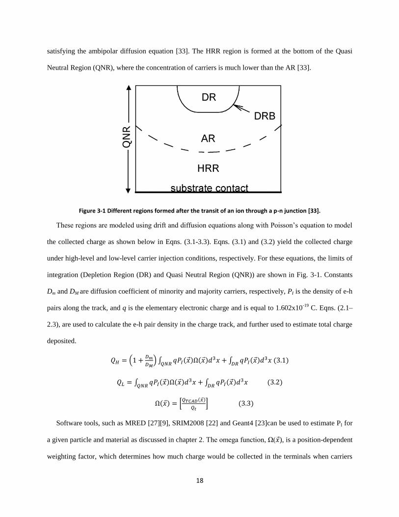
18
satisfying the ambipolar diffusion equation [33]. The HRR region is formed at the bottom of the Quasi
Neutral Region (QNR), where the concentration of carriers is much lower than the AR [33].
Figure 3-1 Different regions formed after the transit of an ion through a p-n junction [33].
These regions are modeled using drift and diffusion equations along with Poisson’s equation to model
the collected charge as shown below in Eqns. (3.1-3.3). Eqns. (3.1) and (3.2) yield the collected charge
under high-level and low-level carrier injection conditions, respectively. For these equations, the limits of
integration (Depletion Region (DR) and Quasi Neutral Region (QNR)) are shown in Fig. 3-1. Constants
Dm and DM are diffusion coefficient of minority and majority carriers, respectively, PI is the density of e-h
pairs along the track, and q is the elementary electronic charge and is equal to 1.602x10⁻¹⁹
C. Eqns. (2.1–
2.3), are used to calculate the e-h pair density in the charge track, and further used to estimate total charge
deposited.
𝑄𝐻 = (1 +𝐷𝑚
𝐷𝑀) ∫ 𝑞𝑃𝐼()Ω()𝑑
3𝑥𝑄𝑁𝑅
+ ∫ 𝑞𝑃𝐼()𝑑3𝑥
𝐷𝑅 (3.1)
𝑄𝐿 = ∫ 𝑞𝑃𝐼()Ω()𝑑3𝑥
𝑄𝑁𝑅+ ∫ 𝑞𝑃𝐼()𝑑
3𝑥𝐷𝑅
(3.2)
Ω() = [𝑄𝑇𝐶𝐴𝐷(𝑥)
𝑄𝑡] (3.3)
Software tools, such as MRED [27][9], SRIM2008 [22] and Geant4 [23]can be used to estimate PI for
a given particle and material as discussed in chapter 2. The omega function, Ω(), is a position-dependent
weighting factor, which determines how much charge would be collected in the terminals when carriers
QNR
19
are generated locally inside the device. Note that Ω() shown in (3.3) is derived using a point source
under low level injection (𝑃𝐼()) is a delta function) [34]. It satisfies the Laplace equation inside the QNR
with appropriate boundary conditions [33] as:
∇2Ω() = 0 𝑖𝑛 𝑄𝑁𝑅 , Ω() = 1 𝑜𝑛 𝐷𝑅𝐵,
Ω() = 0 𝑜𝑛 𝑆𝑢𝑏𝑠𝑡𝑟𝑎𝑡𝑒 𝑐𝑜𝑛𝑡𝑎𝑐𝑡 (3.4)
All the device geometry information is contained in Ω() implicitly. It could only be solved
analytically in certain simple cases, such as 1D simple diode and 3D isolated disk [33] or it could be
probed through two-photon absorption laser experiment [34]. To evaluate the Ω() in device with
complicated structure, TCAD simulations could also be used to construct the functional form by using the
relationship shown in (3). After constructing Ω(), it could predict the charge collection in low-level and
high-level injection conditions based on Eqns. (3.1) and (3,2) assuming that Ω() is the same in both
conditions. [34]. About 6 TCAD simulations were used to estimate the collected charge (QTCAD) and
the total amount of charge generated by the event along the device depth (Qt).
The above model was shown to work for a (~200 µm x ~800 µm) bulk silicon diode [34], but it is not
directly applicable to transistors during a single-event. To apply the ADC model to the transistor case, an
extension of the device model as used in the above discussion is necessary to take into account the
physical differences as well as mechanisms occurring in a transistor, but not in a diode. These differences
include the presence of a substrate contact, well/substrate boundaries, parasitic-bipolar amplification,
charge sharing, and criteria to determine the low- and high-level injection conditions.
With the objective of characterizing the transistor device regions similar to those shown in Fig. 3-1 for
the p-n diode, it was assumed that the bottom cutoff boundary for charge collection for p-type transistors
is at the well boundary, where the well/substrate depletion region forms a secondary junction with the
electric field limiting the collection of holes generated in the substrate. For the n-type transistors, this
bottom cut-off boundary is given by the effective charge collection depth, assuming a dual-well process.
Similar cutoff boundaries have been used before for TCAD SEE simulations [18].
20
For CMOS transistors, the presence of a parasitic bipolar transistor results in additional charge
collection [20] and therefore must be taken into account in the model. As a result, the total collected
charge for a PMOS transistor is the sum of the drift and diffusion currents inside the n-well and the
parasitic-bipolar-amplification current. The parasitic bipolar amplification for NMOS transistors is
assumed to be not significant for a dual-well process [20]. The parasitic-bipolar-amplification current is
incorporated within the omega function for the proposed model as described in section V.
Lastly, to apply this model, it is important to identify device conditions and particle LET values
required to create low and high-level injection. It was shown previously that charge deposition lower than
0.81 pC in the diode (n+p, p doped = 1x10¹⁵
cm-3
) used by [34] creates a low-level injection condition.
Although the specific value delineating high- and low-level injection conditions depends on the particular
structure, this value provides a useful first-order estimate to be used in the proposed model for transistors.
For particle LETs less than 30 MeV*cm2/mg, the total deposited charge in the n-well is less than 0.3 pC,
which is much less than 0.81 pC. In addition, as the technology scales, the n-well doping increases,
requiring higher LET particles to generate high-level injection conditions. Comparing the devices from
[34] and the ones used in this work, the well/substrate doping is between 1 and 3 orders of magnitude
higher, requiring even higher LETs to generate a high-level condition. Also, since the cross section
saturates for most advanced technology nodes for particles with LET equal to or greater than 30
MeV*cm2/mg, the data showed in this work, and the proposed ADC extension, considers low-level
injection conditions.
With the basic framework established to apply the ADC model to the transistor case, the model was
extended to include charge-sharing effects. The objective is to estimate the charge collected by multiple
transistors, given their distance to the ion hit location. Eqns. (3.5-3.7) show the equations used to
accomplish this task.
𝑄𝑞𝑛𝑟 = ∫ 𝑞𝑃𝐼()(1 − Ω())𝑑3𝑥
𝑄𝑁𝑅 (3.5)
𝑄𝐶𝑖 = 𝑄𝑞𝑛𝑟 ∗ Ω𝑑(𝑑) (3.6)
21
Ω𝑑(𝑑) = [𝑄𝑇𝐶𝐴𝐷()
𝑄𝑡] (3.7)
For the above equations, Qqnr is the charge due to the diffusion current and the parasitic bipolar
amplification and QCi is the charge collected at node i. Qqnr is modelled considering that the charge
collected by a secondary transistor will be mainly influenced by the physical conditions of the AR and
HRR regions, since in the DR region, PI(x)=0. This assumption allows Qqnr to be estimated using Eqn.
(3.5). The charge collected at each node (3.6), is then a function of Qqnr and the function Ωd(d). The
function Ωd(d) is used to fit the parasitic-bipolar amplification and diffusion current, and thus is both
technology and device dependent. To estimate Ωd, a few TCAD simulations are required to estimate the
collected charge vs. distance in an array of transistors. With this information, the ratio of collected charge
and charge generated is calculated using Eqn. (3.7), and fitted to a curve to define the distance omega
function, Ωd(d). For the work presented in this paper, the function Ωd was calculated using 8 TCAD
simulations using the Sentaurus [36] simulator from the Synopsys tool set. The number of TCAD
simulations required is small and the simulations need to be carried out only once for a given technology.
A minimum of one simulation for each of the device regions shown in Fig. 3-1 is required for estimating
the Omega function; more simulations will increase the accuracy of the model. More details related to the
omega function estimation are provided in section V.
3.3. Devices, Technology Nodes and Radiation Event
To validate the accuracy of the model, 4 different technology nodes (130, 90, 65 and 40 nm) were
analyzed, based on the availability of TCAD data for the comparison. Table I lists the technology
parameters needed to characterize the devices to be evaluated by the proposed model. Except for the
parameters listed in the table, no additional information regarding the technologies is required for the
proposed model. These parameters are for dual-well, bulk CMOS planar technologies. Data for the 0.13
µm technology were acquired from [20], 90 nm from [21] and 40 nm from [18]. The data for 65 nm were
estimated based on data from the 90 nm and 45 nm technologies.
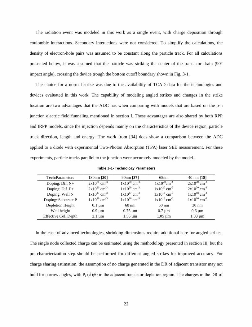
22
The radiation event was modeled in this work as a single event, with charge deposition through
coulombic interactions. Secondary interactions were not considered. To simplify the calculations, the
density of electron-hole pairs was assumed to be constant along the particle track. For all calculations
presented below, it was assumed that the particle was striking the center of the transistor drain (90°
impact angle), crossing the device trough the bottom cutoff boundary shown in Fig. 3-1.
The choice for a normal strike was due to the availability of TCAD data for the technologies and
devices evaluated in this work. The capability of modeling angled strikes and changes in the strike
location are two advantages that the ADC has when comparing with models that are based on the p-n
junction electric field funneling mentioned in section I. These advantages are also shared by both RPP
and IRPP models, since the injection depends mainly on the characteristics of the device region, particle
track direction, length and energy. The work from [34] does show a comparison between the ADC
applied to a diode with experimental Two-Photon Absorption (TPA) laser SEE measurement. For these
experiments, particle tracks parallel to the junction were accurately modeled by the model.
Table 3-1- Technology Parameters
Tech\Parameters 130nm [20] 90nm [37] 65nm 40 nm [18]
Doping: Dif. N+ 2x10²⁰
cm-3
1x10²⁰
cm-3
1x10²⁰
cm-3
2x10²⁰
cm-3
Doping: Dif. P+ 2x10²⁰
cm-3
1x10²⁰
cm-3
1x10²⁰
cm-3
2x10²⁰
cm-3
Doping: Well N 1x10¹⁷
cm-3
1x10¹⁷
cm-3
1x10¹⁸
cm-3
1x10¹⁸
cm-3
Doping: Substrate P 1x10¹⁶
cm-3
1x10¹⁶
cm-3
1x10¹⁶
cm-3
1x10¹⁶
cm-3
Depletion Height 0.1 µm 60 nm 50 nm 30 nm
Well height 0.9 µm 0.75 µm 0.7 µm 0.6 µm
Effective Col. Depth 2.1 µm 1.56 µm 1.05 µm 1.03 µm
In the case of advanced technologies, shrinking dimensions require additional care for angled strikes.
The single node collected charge can be estimated using the methodology presented in section III, but the
pre-characterization step should be performed for different angled strikes for improved accuracy. For
charge sharing estimation, the assumption of no charge generated in the DR of adjacent transistor may not
hold for narrow angles, with PI ()≠0 in the adjacent transistor depletion region. The charges in the DR of
23
nearby transistors have to be calculated with ∫ 𝑞𝑃𝐼()𝑑3𝑥
𝐷𝑅 for each DR in the particle track and added to
the charge estimation (𝑄𝐶𝑖) calculated using Eqn. (3.6).
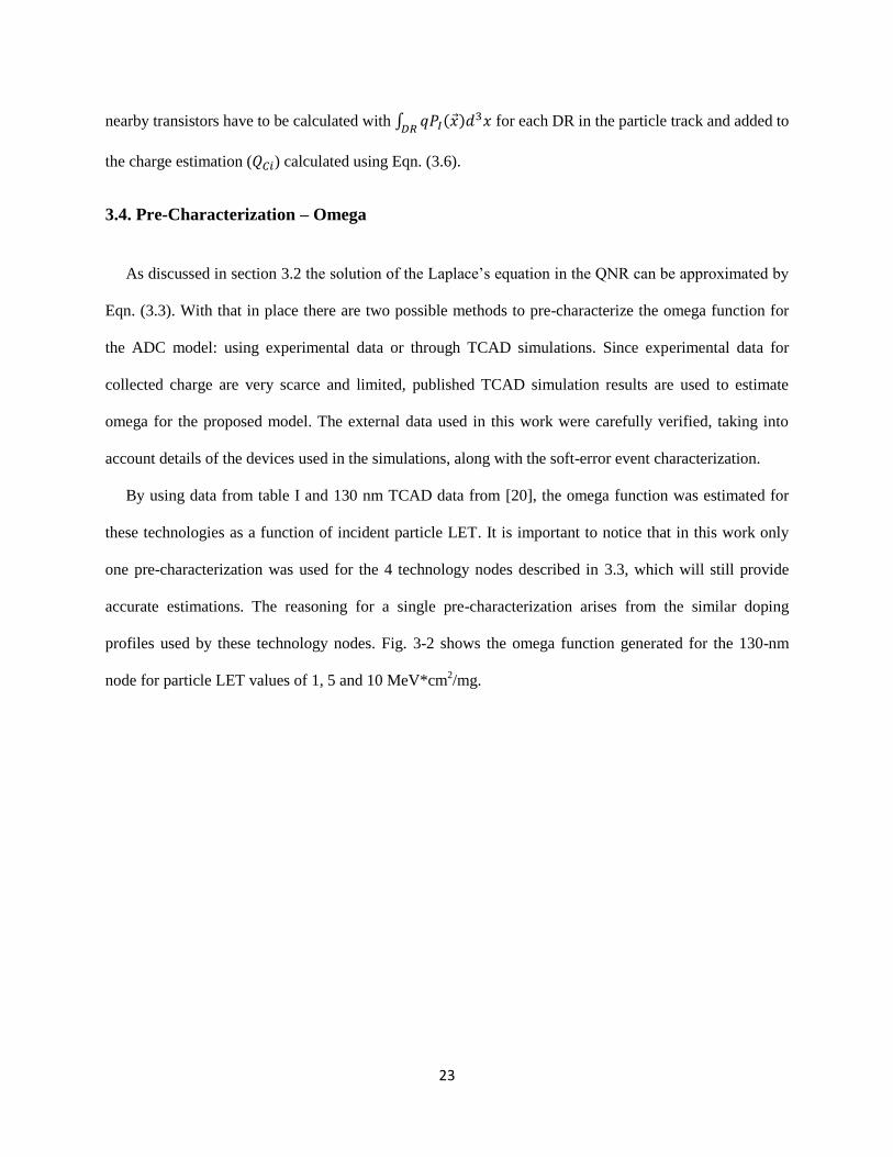
3.4. Pre-Characterization – Omega
As discussed in section 3.2 the solution of the Laplace’s equation in the QNR can be approximated by
Eqn. (3.3). With that in place there are two possible methods to pre-characterize the omega function for
the ADC model: using experimental data or through TCAD simulations. Since experimental data for
collected charge are very scarce and limited, published TCAD simulation results are used to estimate
omega for the proposed model. The external data used in this work were carefully verified, taking into
account details of the devices used in the simulations, along with the soft-error event characterization.
By using data from table I and 130 nm TCAD data from [20], the omega function was estimated for
these technologies as a function of incident particle LET. It is important to notice that in this work only
one pre-characterization was used for the 4 technology nodes described in 3.3, which will still provide
accurate estimations. The reasoning for a single pre-characterization arises from the similar doping
profiles used by these technology nodes. Fig. 3-2 shows the omega function generated for the 130-nm
node for particle LET values of 1, 5 and 10 MeV*cm2/mg.
24
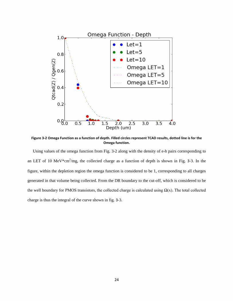
Figure 3-2 Omega Function as a function of depth. Filled circles represent TCAD results, dotted line is for the Omega function.
Using values of the omega function from Fig. 3-2 along with the density of e-h pairs corresponding to
an LET of 10 MeV*cm2/mg, the collected charge as a function of depth is shown in Fig. 3-3. In the
figure, within the depletion region the omega function is considered to be 1, corresponding to all charges
generated in that volume being collected. From the DR boundary to the cut-off, which is considered to be
the well boundary for PMOS transistors, the collected charge is calculated using Ω(x). The total collected
charge is thus the integral of the curve shown in fig. 3-3.
25
Figure 3-3- Collected Charge vs Depth for the 130 nm technology node parameters listed in Table I.
A similar procedure is used to estimate the omega distance function Ωd(d) for the charge sharing Eqn.
(9). Using TCAD data from the 130-nm node, the omega distance function was estimated by measuring
the collected charge on transistors up to 2 μm from the hit location for different particle LET values. Eqn.
(9) is then used to generate the data points for calibration. The secondary devices to collect charge are
modeled in TCAD with the biasing setting the transistors in the “off-state”.
26
Figure 3-4: Omega function as a function of distance. Filled circles represent TCAD data, dotted line is for the Omega
By measuring the Ωd(d) for multiple LETs the accuracy of the model can be improved by selecting the
closest data set according to the LET used as input in the model.
3.5 Single Node Collected Charge
To validate the applicability of the proposed additions to the ADC model to estimate single node
collected charge, the model is compared with TCAD simulation data and both RPP and IRPP estimations.
The RPP and IRPP models can both be analytically represented with the nested sensitive volume Eqn.
(3.8) [38], where α is a weighting coefficient and E the deposited energy. The first term of the equation is
the energy to charge conversion factor assuming that 3.6 eV are required to produce an electron-hole pair
[24].
Notice in this thesis the IRPP model is calculated considering multiple sensitive volumes. The IRPP
model therefore requires the definition of sensitive volumes (SV) and collection coefficients (αi). For this
work sensitive volumes were defined based on the guidelines from [39], and the collection coefficients
were estimated using 130nm technology data. For these devices a set of four SV, named as SV1, SV2,
27
SV3 and SV4 with collection coefficients 1, 0.62, 0.3 and 0.06, respectively, were used. The height of
each SV has to be calculated for each technology, with the SV1 height being the DR height and SV2,
SV3 and SV4 heights being approximately 30, 30, and 40%, respectively, of the distance from the DR to
the well boundary for the p-type transistors (and effective collection depth for the n-type transistors). The
RPP model can be seen as a single SV, with a constant collection coefficient.
𝑄𝑐 ≈1𝑝𝐶
22.5 𝑀𝑒𝑉∑𝛼𝑖𝐸𝑖
𝑁
𝑖=1
(3.8)
For a better comparison the RPP collection coefficient was fitted using 130nm technology data, and
for these computations was set to be 0.8. The collection coefficients used by both RPP and IRPP were set
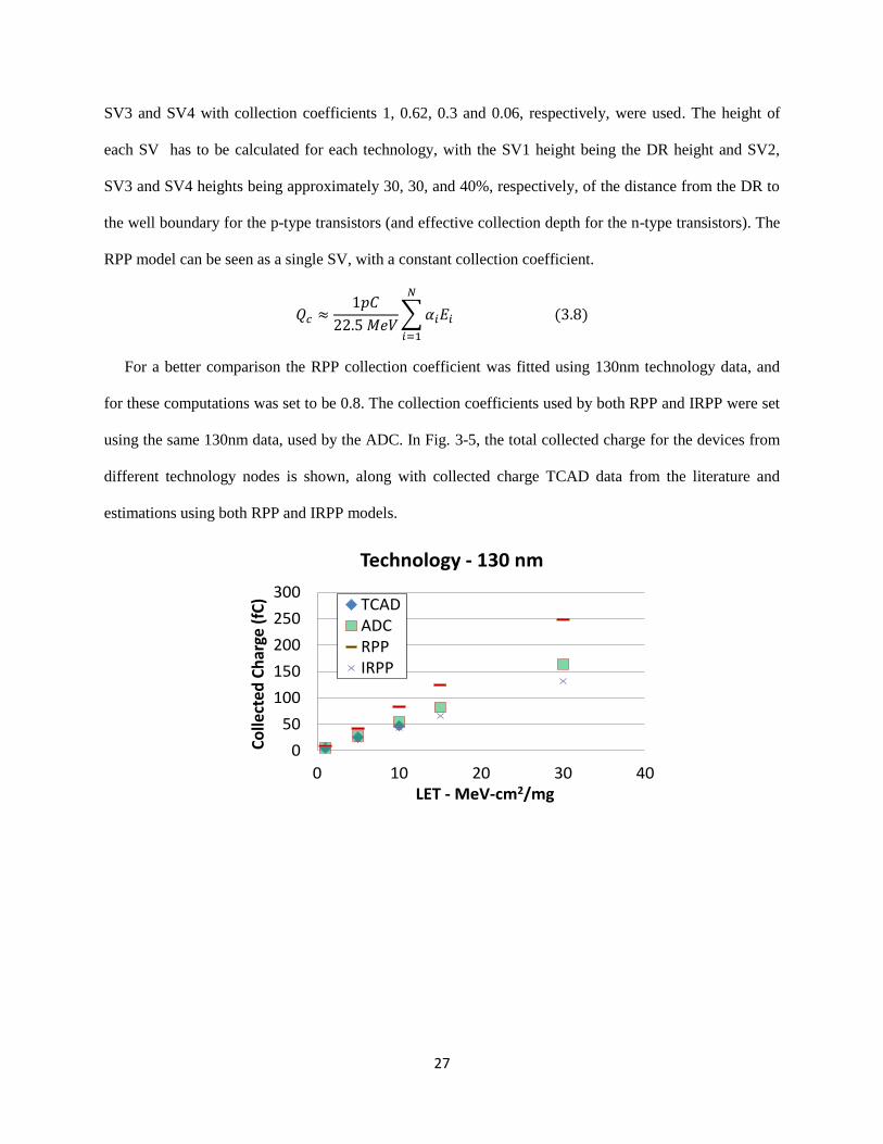
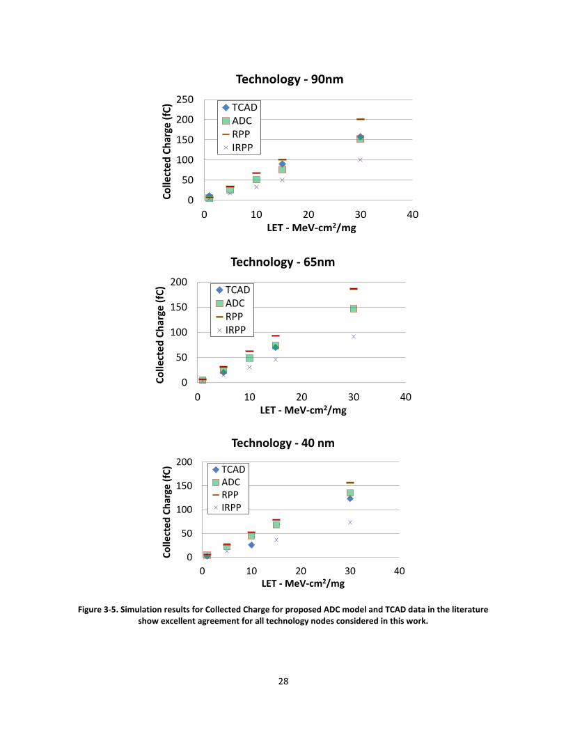
using the same 130nm data, used by the ADC. In Fig. 3-5, the total collected charge for the devices from
different technology nodes is shown, along with collected charge TCAD data from the literature and
estimations using both RPP and IRPP models.
0
50
100
150
200
250
300
0 10 20 30 40
Co
llect
ed C
har
ge (
fC)
LET - MeV-cm2/mg
Technology - 130 nm
TCADADCRPPIRPP
28
Figure 3-5. Simulation results for Collected Charge for proposed ADC model and TCAD data in the literature show excellent agreement for all technology nodes considered in this work.
0
50
100
150
200
250
0 10 20 30 40
Co
llect
ed C
har
ge (
fC)
LET - MeV-cm2/mg
Technology - 90nm
TCADADCRPPIRPP
0
50
100
150
200
0 10 20 30 40
Co
llect
ed
Ch
arge
(fC
)
LET - MeV-cm2/mg
Technology - 65nm
TCADADCRPPIRPP
0
50
100
150
200
0 10 20 30 40
Co
llect
ed C
har
ge (
fC)
LET - MeV-cm2/mg
Technology - 40 nm
TCADADCRPPIRPP
29
The PMOS transistor data from the proposed model are compared with data from [26, 40, 41] and [20]
for the 40, 90, 65, 130 nm technologies, respectively. The TCAD data mentioned before were validated,
by verifying both the devices used in simulations and the physical models set in the simulations. These
simulations were carried out using standard drift-diffusion models, carrier-carrier scattering models and
both Shockley-Read-Hall and Auger recombination models. The heavy ion simulations were set with a
track long enough to cross the devices, and the charge was distributed along the track with a Gaussian
profile, a common practice when simulating soft error events.
For the technologies compared in this work, the results indicate that the values of collected charge
estimated by the proposed ADC model are very close to the TCAD data reported in the literature. For
very low particle LET values, ~1 MeV*cm2/mg all models show excellent agreement with TCAD data.
However, as the particle LET values increase, the collected charge estimations of both RPP and IRPP
models start to deviate from TCAD data.
3.6. Error Comparison between ADC, RPP and IRPP
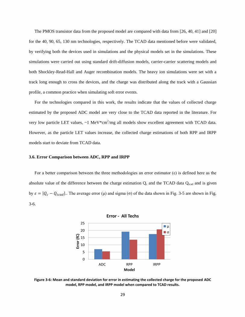
For a better comparison between the three methodologies an error estimator (ε) is defined here as the
absolute value of the difference between the charge estimation Qc and the TCAD data Qtcad and is given
by 𝜀 = |𝑄𝑐 − 𝑄𝑡𝑐𝑎𝑑|.. The average error (μ) and sigma (σ) of the data shown in Fig. 3-5 are shown in Fig.
3-6.
Figure 3-6: Mean and standard deviation for error in estimating the collected charge for the proposed ADC model, RPP model, and IRPP model when compared to TCAD results.
0
5
10
15
20
25
ADC RPP IRPP
Erro
r (f
C)
Model
Error - All Techs
μ
σ
30
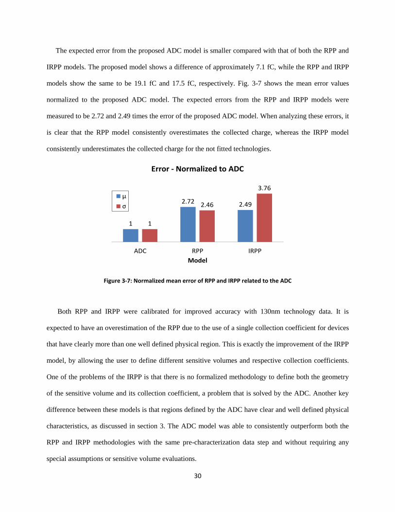
The expected error from the proposed ADC model is smaller compared with that of both the RPP and
IRPP models. The proposed model shows a difference of approximately 7.1 fC, while the RPP and IRPP
models show the same to be 19.1 fC and 17.5 fC, respectively. Fig. 3-7 shows the mean error values
normalized to the proposed ADC model. The expected errors from the RPP and IRPP models were
measured to be 2.72 and 2.49 times the error of the proposed ADC model. When analyzing these errors, it
is clear that the RPP model consistently overestimates the collected charge, whereas the IRPP model
consistently underestimates the collected charge for the not fitted technologies.
Figure 3-7: Normalized mean error of RPP and IRPP related to the ADC
Both RPP and IRPP were calibrated for improved accuracy with 130nm technology data. It is
expected to have an overestimation of the RPP due to the use of a single collection coefficient for devices
that have clearly more than one well defined physical region. This is exactly the improvement of the IRPP
model, by allowing the user to define different sensitive volumes and respective collection coefficients.
One of the problems of the IRPP is that there is no formalized methodology to define both the geometry
of the sensitive volume and its collection coefficient, a problem that is solved by the ADC. Another key
difference between these models is that regions defined by the ADC have clear and well defined physical
characteristics, as discussed in section 3. The ADC model was able to consistently outperform both the
RPP and IRPP methodologies with the same pre-characterization data step and without requiring any
special assumptions or sensitive volume evaluations.
1
2.72 2.49
1
2.46
3.76
ADC RPP IRPP
Model
Error - Normalized to ADC
μ
σ
31
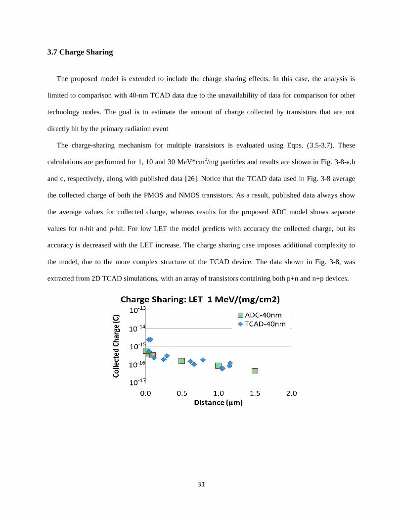
3.7 Charge Sharing
The proposed model is extended to include the charge sharing effects. In this case, the analysis is
limited to comparison with 40-nm TCAD data due to the unavailability of data for comparison for other
technology nodes. The goal is to estimate the amount of charge collected by transistors that are not
directly hit by the primary radiation event
The charge-sharing mechanism for multiple transistors is evaluated using Eqns. (3.5-3.7). These
calculations are performed for 1, 10 and 30 MeV*cm2/mg particles and results are shown in Fig. 3-8-a,b
and c, respectively, along with published data [26]. Notice that the TCAD data used in Fig. 3-8 average
the collected charge of both the PMOS and NMOS transistors. As a result, published data always show
the average values for collected charge, whereas results for the proposed ADC model shows separate
values for n-hit and p-hit. For low LET the model predicts with accuracy the collected charge, but its
accuracy is decreased with the LET increase. The charge sharing case imposes additional complexity to
the model, due to the more complex structure of the TCAD device. The data shown in Fig. 3-8, was
extracted from 2D TCAD simulations, with an array of transistors containing both p+n and n+p devices.
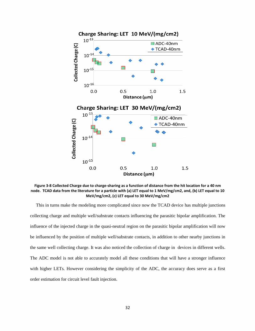
32
Figure 3-8 Collected Charge due to charge-sharing as a function of distance from the hit location for a 40 nm node. TCAD data from the literature for a particle with (a) LET equal to 1 MeV/mg/cm2, and, (b) LET equal to 10
MeV/mg/cm2, (c) LET equal to 30 MeV/mg/cm2
This in turns make the modeling more complicated since now the TCAD device has multiple junctions
collecting charge and multiple well/substrate contacts influencing the parasitic bipolar amplification. The
influence of the injected charge in the quasi-neutral region on the parasitic bipolar amplification will now
be influenced by the position of multiple well/substrate contacts, in addition to other nearby junctions in
the same well collecting charge. It was also noticed the collection of charge in devices in different wells.
The ADC model is not able to accurately model all these conditions that will have a stronger influence
with higher LETs. However considering the simplicity of the ADC, the accuracy does serve as a first
order estimation for circuit level fault injection.

33
3.8 Conclusions
It is shown that the ADC model can be used to estimate the collected charge for multiple transistors in
bulk nanometer scale technologies. Through technology characterization by TCAD simulations, a single
omega function is shown to be adequate to model the collected charge for the hit node and other nearby
nodes. When comparing the ADC model with both RPP and IRPP models, the error of these
methodologies was measured to be about 2.72x and 2.49x higher respectively when compared with the
ADC results. It was also shown that the proposed ADC extension was able to accurately estimate charge
sharing, showing good agreement between estimates and 40-nm TCAD data. The simple formulation of
the ADC model and its accuracy for collected charge estimation make this model a great candidate to be
integrated into the EDA design flow and for circuit level fault injection simulations.
.
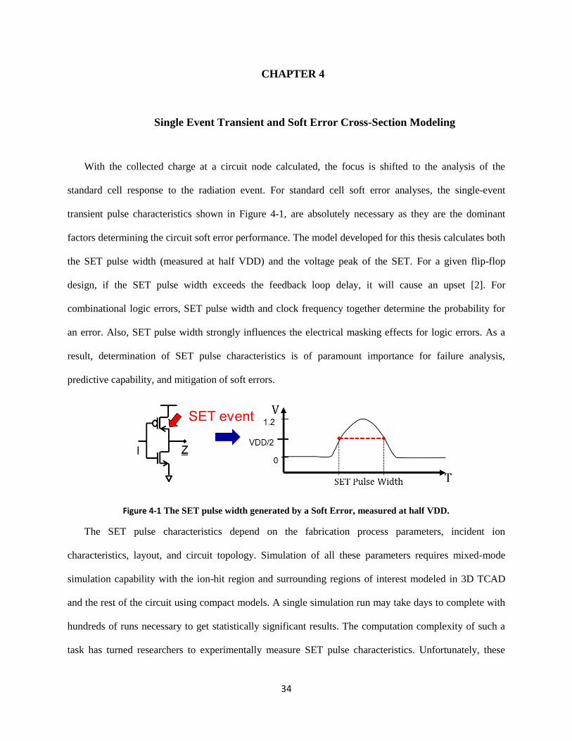
34
CHAPTER 4
4. Single Event Transient and Soft Error Cross-Section Modeling
With the collected charge at a circuit node calculated, the focus is shifted to the analysis of the
standard cell response to the radiation event. For standard cell soft error analyses, the single-event
transient pulse characteristics shown in Figure 4-1, are absolutely necessary as they are the dominant
factors determining the circuit soft error performance. The model developed for this thesis calculates both
the SET pulse width (measured at half VDD) and the voltage peak of the SET. For a given flip-flop
design, if the SET pulse width exceeds the feedback loop delay, it will cause an upset [2]. For
combinational logic errors, SET pulse width and clock frequency together determine the probability for
an error. Also, SET pulse width strongly influences the electrical masking effects for logic errors. As a
result, determination of SET pulse characteristics is of paramount importance for failure analysis,
predictive capability, and mitigation of soft errors.
Figure 4-1 The SET pulse width generated by a Soft Error, measured at half VDD.
The SET pulse characteristics depend on the fabrication process parameters, incident ion
characteristics, layout, and circuit topology. Simulation of all these parameters requires mixed-mode
simulation capability with the ion-hit region and surrounding regions of interest modeled in 3D TCAD
and the rest of the circuit using compact models. A single simulation run may take days to complete with
hundreds of runs necessary to get statistically significant results. The computation complexity of such a
task has turned researchers to experimentally measure SET pulse characteristics. Unfortunately, these
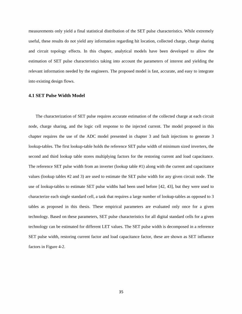
35
measurements only yield a final statistical distribution of the SET pulse characteristics. While extremely
useful, these results do not yield any information regarding hit location, collected charge, charge sharing
and circuit topology effects. In this chapter, analytical models have been developed to allow the
estimation of SET pulse characteristics taking into account the parameters of interest and yielding the
relevant information needed by the engineers. The proposed model is fast, accurate, and easy to integrate
into existing design flows.
4.1 SET Pulse Width Model
The characterization of SET pulse requires accurate estimation of the collected charge at each circuit
node, charge sharing, and the logic cell response to the injected current. The model proposed in this
chapter requires the use of the ADC model presented in chapter 3 and fault injections to generate 3
lookup-tables. The first lookup-table holds the reference SET pulse width of minimum sized inverters, the
second and third lookup table stores multiplying factors for the restoring current and load capacitance.
The reference SET pulse width from an inverter (lookup table #1) along with the current and capacitance
values (lookup tables #2 and 3) are used to estimate the SET pulse width for any given circuit node. The
use of lookup-tables to estimate SET pulse widths had been used before [42, 43], but they were used to
characterize each single standard cell, a task that requires a large number of lookup-tables as opposed to 3
tables as proposed in this thesis. These empirical parameters are evaluated only once for a given
technology. Based on these parameters, SET pulse characteristics for all digital standard cells for a given
technology can be estimated for different LET values. The SET pulse width is decomposed in a reference
SET pulse width, restoring current factor and load capacitance factor, these are shown as SET influence
factors in Figure 4-2.
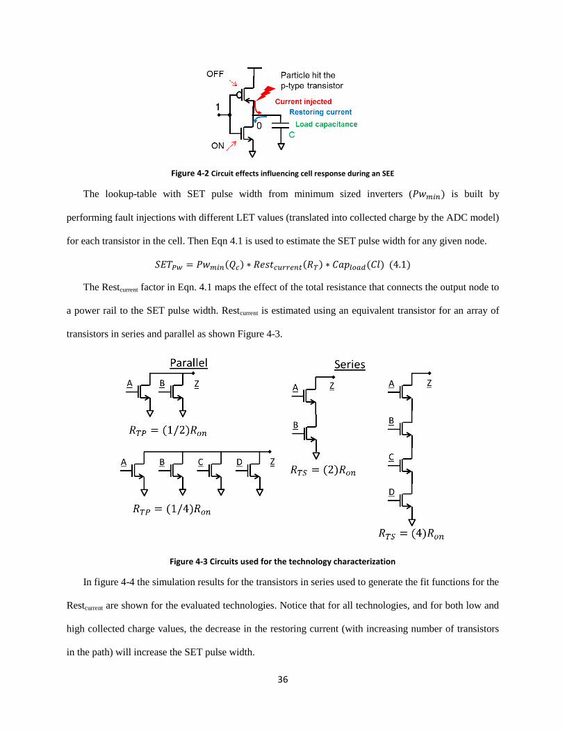
36
Figure 4-2 Circuit effects influencing cell response during an SEE
The lookup-table with SET pulse width from minimum sized inverters (𝑃𝑤𝑚𝑖𝑛) is built by
performing fault injections with different LET values (translated into collected charge by the ADC model)
for each transistor in the cell. Then Eqn 4.1 is used to estimate the SET pulse width for any given node.
𝑆𝐸𝑇𝑃𝑤 = 𝑃𝑤𝑚𝑖𝑛(𝑄𝑐) ∗ 𝑅𝑒𝑠𝑡𝑐𝑢𝑟𝑟𝑒𝑛𝑡(𝑅𝑇) ∗ 𝐶𝑎𝑝𝑙𝑜𝑎𝑑(𝐶𝑙) (4.1)
The Restcurrent factor in Eqn. 4.1 maps the effect of the total resistance that connects the output node to
a power rail to the SET pulse width. Restcurrent is estimated using an equivalent transistor for an array of
transistors in series and parallel as shown Figure 4-3.
Figure 4-3 Circuits used for the technology characterization
In figure 4-4 the simulation results for the transistors in series used to generate the fit functions for the
Restcurrent are shown for the evaluated technologies. Notice that for all technologies, and for both low and
high collected charge values, the decrease in the restoring current (with increasing number of transistors
in the path) will increase the SET pulse width.
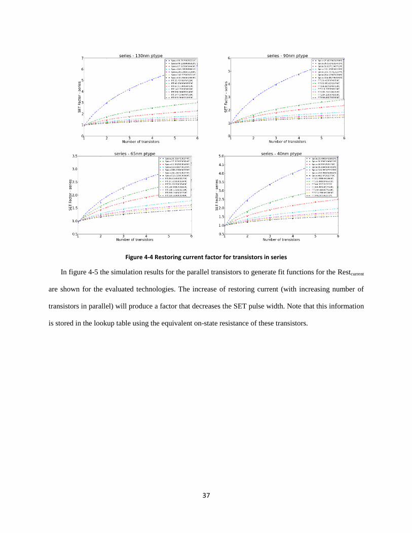
37
Figure 4-4 Restoring current factor for transistors in series
In figure 4-5 the simulation results for the parallel transistors to generate fit functions for the Restcurrent
are shown for the evaluated technologies. The increase of restoring current (with increasing number of
transistors in parallel) will produce a factor that decreases the SET pulse width. Note that this information
is stored in the lookup table using the equivalent on-state resistance of these transistors.

38
Figure 4-5 Restoring current factor for transistors in parallel
The Capload factor is the effect of the load capacitance at an output node on the SET Pulse width.
Lookup Table #3 is used to map different capacitance values at an output node and the reference SET
pulse width from an inverter to estimate the SET pulse width at the node in question. In figure 4-6 the
multiplication factor as a function of Capload is shown for 130, 90, 65 and 40nm technologies.
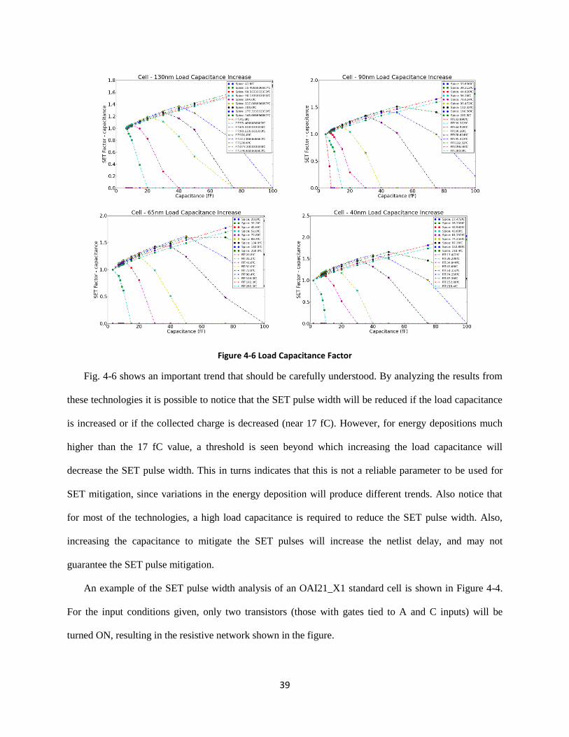
39
Figure 4-6 Load Capacitance Factor
Fig. 4-6 shows an important trend that should be carefully understood. By analyzing the results from
these technologies it is possible to notice that the SET pulse width will be reduced if the load capacitance
is increased or if the collected charge is decreased (near 17 fC). However, for energy depositions much
higher than the 17 fC value, a threshold is seen beyond which increasing the load capacitance will
decrease the SET pulse width. This in turns indicates that this is not a reliable parameter to be used for
SET mitigation, since variations in the energy deposition will produce different trends. Also notice that
for most of the technologies, a high load capacitance is required to reduce the SET pulse width. Also,
increasing the capacitance to mitigate the SET pulses will increase the netlist delay, and may not
guarantee the SET pulse mitigation.
An example of the SET pulse width analysis of an OAI21_X1 standard cell is shown in Figure 4-4.
For the input conditions given, only two transistors (those with gates tied to A and C inputs) will be
turned ON, resulting in the resistive network shown in the figure.
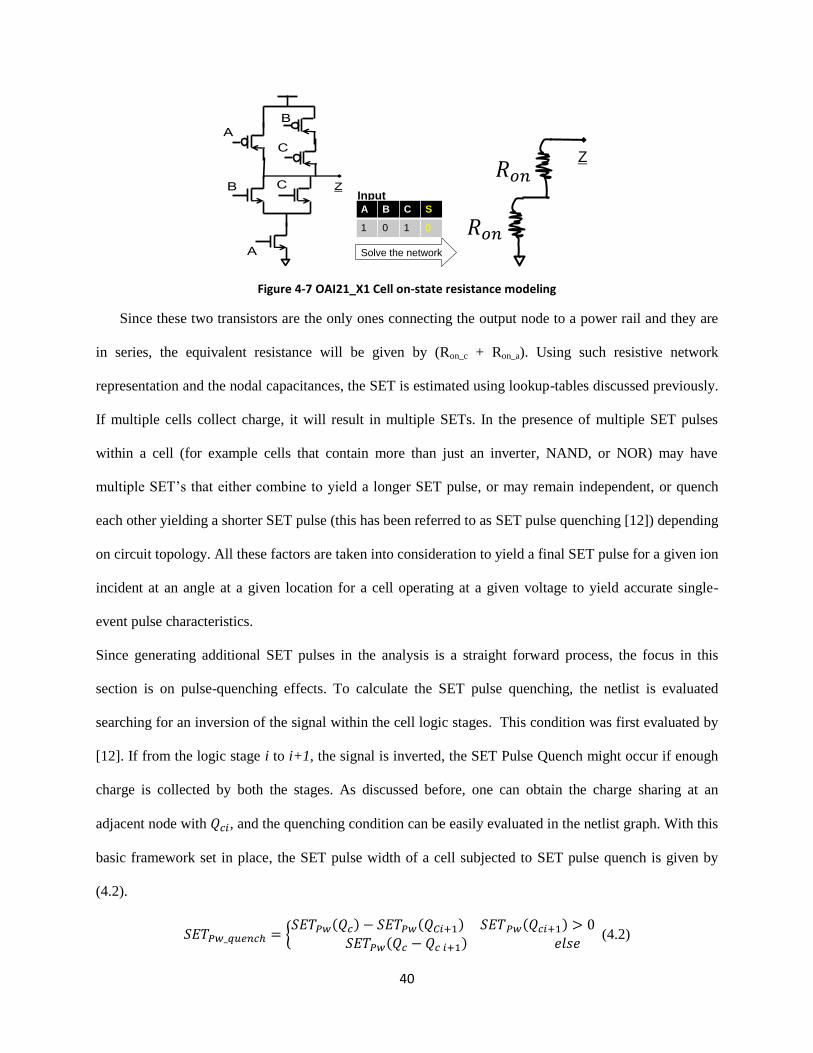
40
Figure 4-7 OAI21_X1 Cell on-state resistance modeling
Since these two transistors are the only ones connecting the output node to a power rail and they are
in series, the equivalent resistance will be given by (Ron_c + Ron_a). Using such resistive network
representation and the nodal capacitances, the SET is estimated using lookup-tables discussed previously.
If multiple cells collect charge, it will result in multiple SETs. In the presence of multiple SET pulses
within a cell (for example cells that contain more than just an inverter, NAND, or NOR) may have
multiple SET’s that either combine to yield a longer SET pulse, or may remain independent, or quench
each other yielding a shorter SET pulse (this has been referred to as SET pulse quenching [12]) depending
on circuit topology. All these factors are taken into consideration to yield a final SET pulse for a given ion
incident at an angle at a given location for a cell operating at a given voltage to yield accurate single-
event pulse characteristics.
Since generating additional SET pulses in the analysis is a straight forward process, the focus in this
section is on pulse-quenching effects. To calculate the SET pulse quenching, the netlist is evaluated
searching for an inversion of the signal within the cell logic stages. This condition was first evaluated by
[12]. If from the logic stage i to i+1, the signal is inverted, the SET Pulse Quench might occur if enough
charge is collected by both the stages. As discussed before, one can obtain the charge sharing at an
adjacent node with 𝑄𝑐𝑖, and the quenching condition can be easily evaluated in the netlist graph. With this
basic framework set in place, the SET pulse width of a cell subjected to SET pulse quench is given by
(4.2).
𝑆𝐸𝑇𝑃𝑤_𝑞𝑢𝑒𝑛𝑐ℎ = 𝑆𝐸𝑇𝑃𝑤(𝑄𝑐) − 𝑆𝐸𝑇𝑃𝑤(𝑄𝐶𝑖+1) 𝑆𝐸𝑇𝑃𝑤(𝑄𝑐𝑖+1) > 0
𝑆𝐸𝑇𝑃𝑤(𝑄𝑐 − 𝑄𝑐 𝑖+1) 𝑒𝑙𝑠𝑒 (4.2)
InputA B C S
1 0 1 0
Solve the network
Z
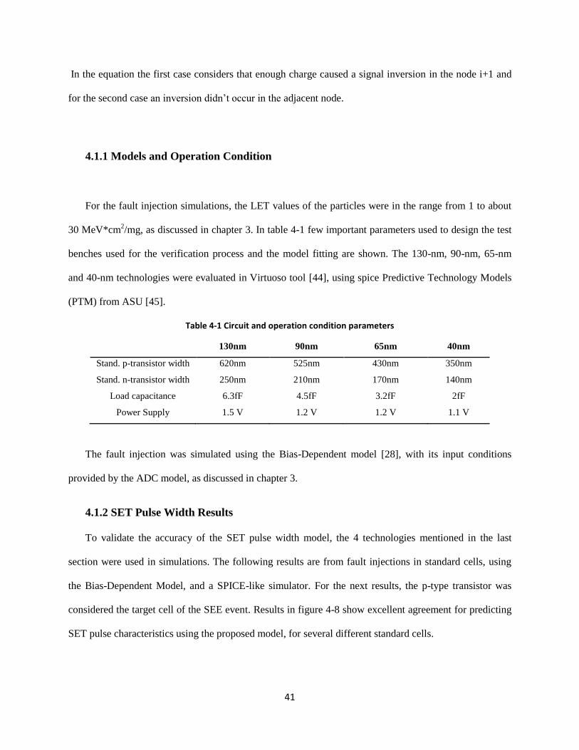
41
In the equation the first case considers that enough charge caused a signal inversion in the node i+1 and
for the second case an inversion didn’t occur in the adjacent node.
4.1.1 Models and Operation Condition
For the fault injection simulations, the LET values of the particles were in the range from 1 to about
30 MeV*cm2/mg, as discussed in chapter 3. In table 4-1 few important parameters used to design the test
benches used for the verification process and the model fitting are shown. The 130-nm, 90-nm, 65-nm
and 40-nm technologies were evaluated in Virtuoso tool [44], using spice Predictive Technology Models
(PTM) from ASU [45].
Table 4-1 Circuit and operation condition parameters
130nm 90nm 65nm 40nm
Stand. p-transistor width 620nm 525nm 430nm 350nm
Stand. n-transistor width 250nm 210nm 170nm 140nm
Load capacitance 6.3fF 4.5fF 3.2fF 2fF
Power Supply 1.5 V 1.2 V 1.2 V 1.1 V
The fault injection was simulated using the Bias-Dependent model [28], with its input conditions
provided by the ADC model, as discussed in chapter 3.
4.1.2 SET Pulse Width Results
To validate the accuracy of the SET pulse width model, the 4 technologies mentioned in the last
section were used in simulations. The following results are from fault injections in standard cells, using
the Bias-Dependent Model, and a SPICE-like simulator. For the next results, the p-type transistor was
considered the target cell of the SEE event. Results in figure 4-8 show excellent agreement for predicting
SET pulse characteristics using the proposed model, for several different standard cells.
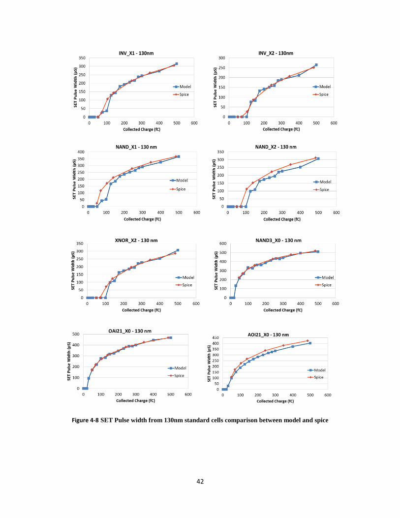
42
Figure 4-8 SET Pulse width from 130nm standard cells comparison between model and spice

43
Notice in figure 4-8 for 130-nm technology node that cells with different sizing and number of inputs
were properly characterized by the SET model. In Figure 4-9, other standard cells that were evaluated for
the 90-, 65- and 40-nm technology nodes are shown with the SET model displaying very good accuracy.
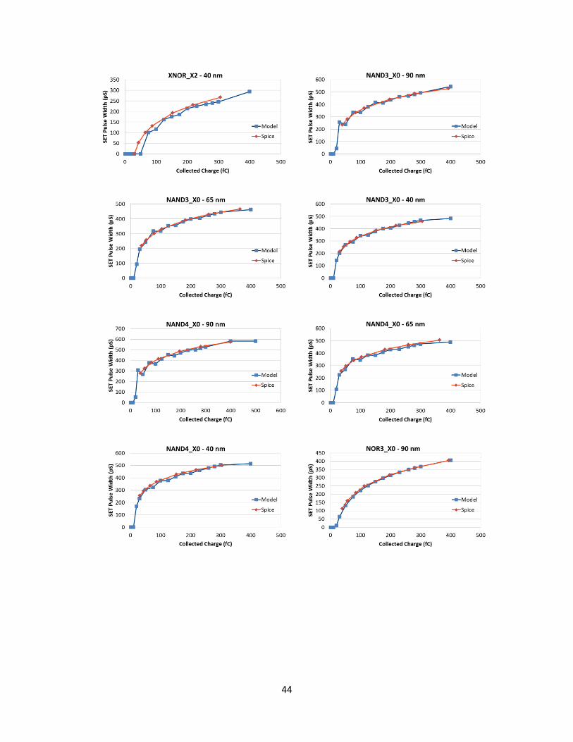
44
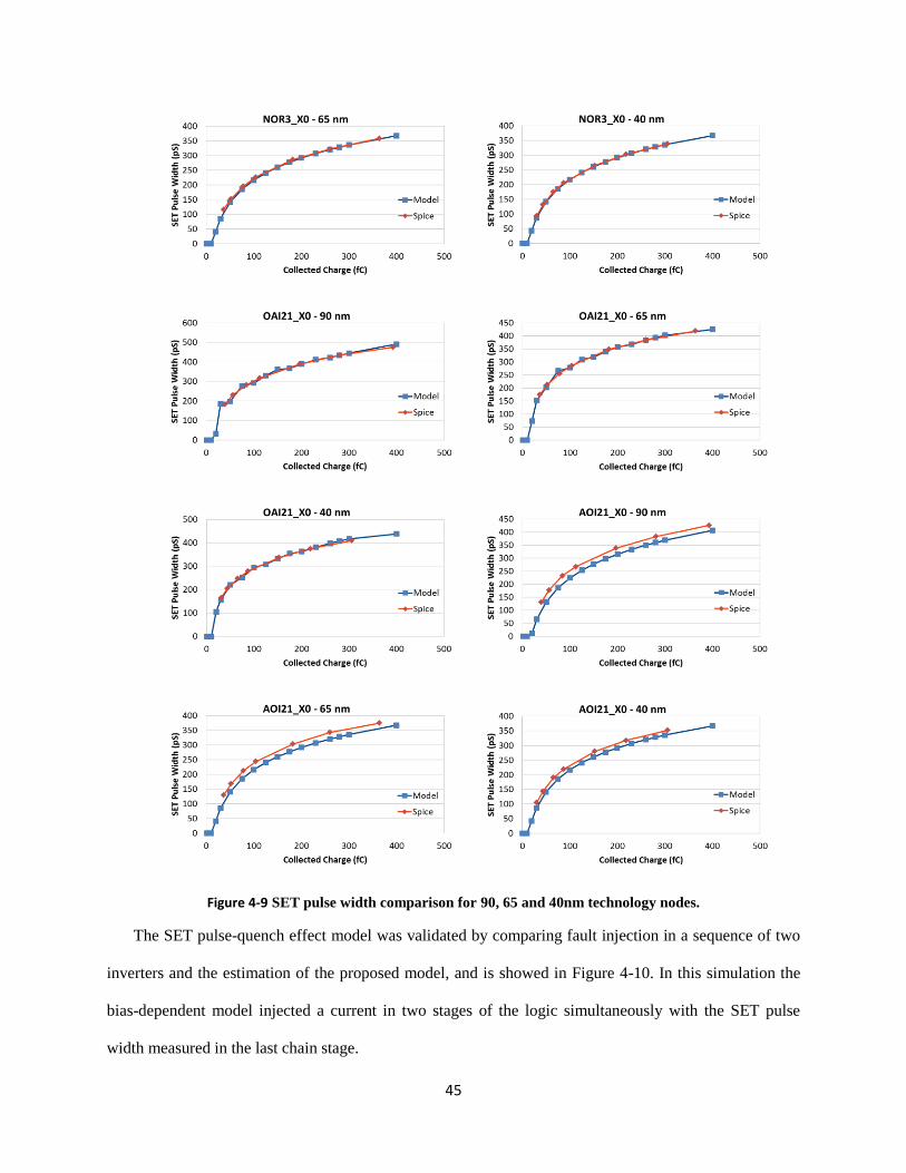
45
Figure 4-9 SET pulse width comparison for 90, 65 and 40nm technology nodes.
The SET pulse-quench effect model was validated by comparing fault injection in a sequence of two
inverters and the estimation of the proposed model, and is showed in Figure 4-10. In this simulation the
bias-dependent model injected a current in two stages of the logic simultaneously with the SET pulse
width measured in the last chain stage.
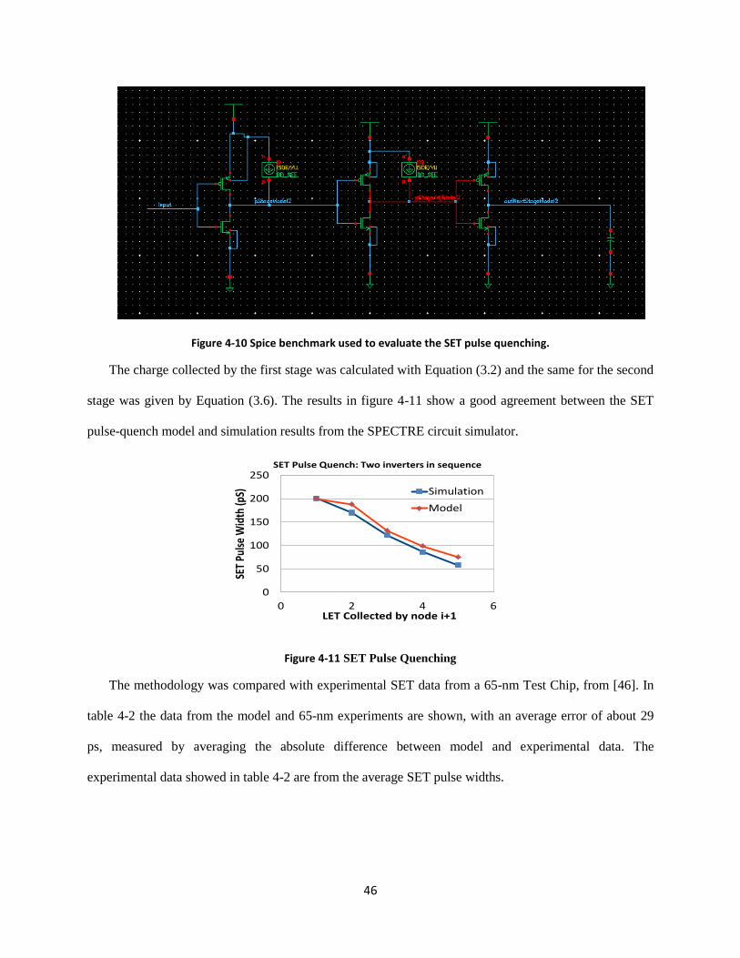
46
Figure 4-10 Spice benchmark used to evaluate the SET pulse quenching.
The charge collected by the first stage was calculated with Equation (3.2) and the same for the second
stage was given by Equation (3.6). The results in figure 4-11 show a good agreement between the SET
pulse-quench model and simulation results from the SPECTRE circuit simulator.
Figure 4-11 SET Pulse Quenching
The methodology was compared with experimental SET data from a 65-nm Test Chip, from [46]. In
table 4-2 the data from the model and 65-nm experiments are shown, with an average error of about 29
ps, measured by averaging the absolute difference between model and experimental data. The
experimental data showed in table 4-2 are from the average SET pulse widths.
0 2 4 6
0
50
100
150
200
250
LET Collected by node i+1
SET
Puls
e W
idth
(pS)
SET Pulse Quench: Two inverters in sequence
Simulation
Model
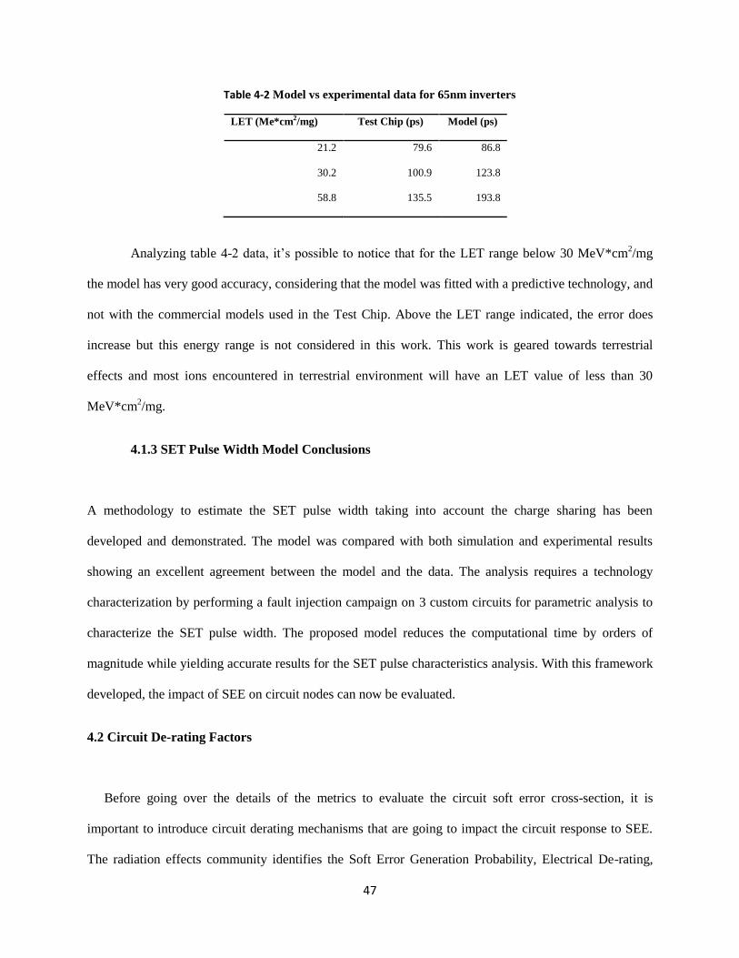
47
Table 4-2 Model vs experimental data for 65nm inverters
LET (Me*cm2/mg) Test Chip (ps) Model (ps)
21.2 79.6 86.8
30.2 100.9 123.8
58.8 135.5 193.8
Analyzing table 4-2 data, it’s possible to notice that for the LET range below 30 MeV*cm2/mg
the model has very good accuracy, considering that the model was fitted with a predictive technology, and
not with the commercial models used in the Test Chip. Above the LET range indicated, the error does
increase but this energy range is not considered in this work. This work is geared towards terrestrial
effects and most ions encountered in terrestrial environment will have an LET value of less than 30
MeV*cm2/mg.
4.1.3 SET Pulse Width Model Conclusions
A methodology to estimate the SET pulse width taking into account the charge sharing has been
developed and demonstrated. The model was compared with both simulation and experimental results
showing an excellent agreement between the model and the data. The analysis requires a technology
characterization by performing a fault injection campaign on 3 custom circuits for parametric analysis to
characterize the SET pulse width. The proposed model reduces the computational time by orders of
magnitude while yielding accurate results for the SET pulse characteristics analysis. With this framework
developed, the impact of SEE on circuit nodes can now be evaluated.
4.2 Circuit De-rating Factors
Before going over the details of the metrics to evaluate the circuit soft error cross-section, it is
important to introduce circuit derating mechanisms that are going to impact the circuit response to SEE.
The radiation effects community identifies the Soft Error Generation Probability, Electrical De-rating,
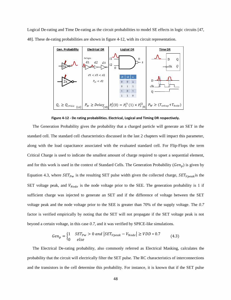
48
Logical De-rating and Time De-rating as the circuit probabilities to model SE effects in logic circuits [47,
48]. These de-rating probabilities are shown in figure 4-12, with its circuit representation.
Figure 4-12 - De rating probabilities. Electrical, Logical and Timing DR respectively.
The Generation Probability gives the probability that a charged particle will generate an SET in the
standard cell. The standard cell characteristics discussed in the last 2 chapters will impact this parameter,
along with the load capacitance associated with the evaluated standard cell. For Flip-Flops the term
Critical Charge is used to indicate the smallest amount of charge required to upset a sequential element,
and for this work is used in the context of Standard Cells. The Generation Probability (𝐺𝑒𝑛𝑝) is given by
Equation 4.3, where 𝑆𝐸𝑇𝑃𝑤 is the resulting SET pulse width given the collected charge, 𝑆𝐸𝑇𝑉𝑝𝑒𝑎𝑘is the
SET voltage peak, and 𝑉𝑁𝑜𝑑𝑒 is the node voltage prior to the SEE. The generation probability is 1 if
sufficient charge was injected to generate an SET and if the difference of voltage between the SET
voltage peak and the node voltage prior to the SEE is greater than 70% of the supply voltage. The 0.7
factor is verified empirically by noting that the SET will not propagate if the SET voltage peak is not
beyond a certain voltage, in this case 0.7, and it was verified by SPICE-like simulations.
𝐺𝑒𝑛𝑝 = 1 𝑆𝐸𝑇𝑃𝑤 > 0 𝑎𝑛𝑑 |𝑆𝐸𝑇𝑉𝑝𝑒𝑎𝑘 − 𝑉𝑁𝑜𝑑𝑒| ≥ 𝑉𝐷𝐷 ∗ 0.7
0 𝑒𝑙𝑠𝑒 (4.3)
The Electrical De-rating probability, also commonly referred as Electrical Masking, calculates the
probability that the circuit will electrically filter the SET pulse. The RC characteristics of interconnections
and the transistors in the cell determine this probability. For instance, it is known that if the SET pulse
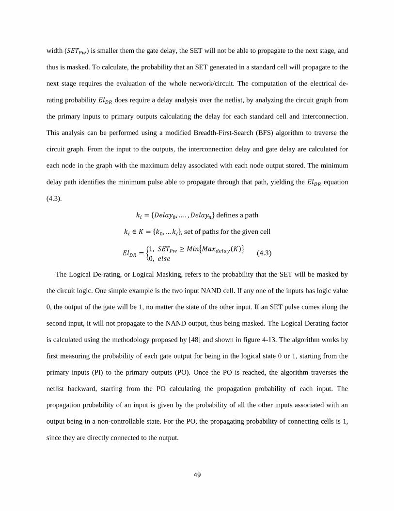
49
width (𝑆𝐸𝑇𝑃𝑤) is smaller them the gate delay, the SET will not be able to propagate to the next stage, and
thus is masked. To calculate, the probability that an SET generated in a standard cell will propagate to the
next stage requires the evaluation of the whole network/circuit. The computation of the electrical de-
rating probability 𝐸𝑙𝐷𝑅 does require a delay analysis over the netlist, by analyzing the circuit graph from
the primary inputs to primary outputs calculating the delay for each standard cell and interconnection.
This analysis can be performed using a modified Breadth-First-Search (BFS) algorithm to traverse the
circuit graph. From the input to the outputs, the interconnection delay and gate delay are calculated for
each node in the graph with the maximum delay associated with each node output stored. The minimum
delay path identifies the minimum pulse able to propagate through that path, yielding the 𝐸𝑙𝐷𝑅 equation
(4.3).
𝑘𝑖 = 𝐷𝑒𝑙𝑎𝑦0, … . , 𝐷𝑒𝑙𝑎𝑦𝑛 defines a path
𝑘𝑖 ∈ 𝐾 = 𝑘0, … 𝑘𝑙, set of paths for the given cell
𝐸𝑙𝐷𝑅 = 1, 𝑆𝐸𝑇𝑃𝑤 ≥ 𝑀𝑖𝑛𝑀𝑎𝑥𝑑𝑒𝑙𝑎𝑦(𝐾)
0, 𝑒𝑙𝑠𝑒 (4.3)
The Logical De-rating, or Logical Masking, refers to the probability that the SET will be masked by
the circuit logic. One simple example is the two input NAND cell. If any one of the inputs has logic value
0, the output of the gate will be 1, no matter the state of the other input. If an SET pulse comes along the
second input, it will not propagate to the NAND output, thus being masked. The Logical Derating factor
is calculated using the methodology proposed by [48] and shown in figure 4-13. The algorithm works by
first measuring the probability of each gate output for being in the logical state 0 or 1, starting from the
primary inputs (PI) to the primary outputs (PO). Once the PO is reached, the algorithm traverses the
netlist backward, starting from the PO calculating the propagation probability of each input. The
propagation probability of an input is given by the probability of all the other inputs associated with an
output being in a non-controllable state. For the PO, the propagating probability of connecting cells is 1,
since they are directly connected to the output.
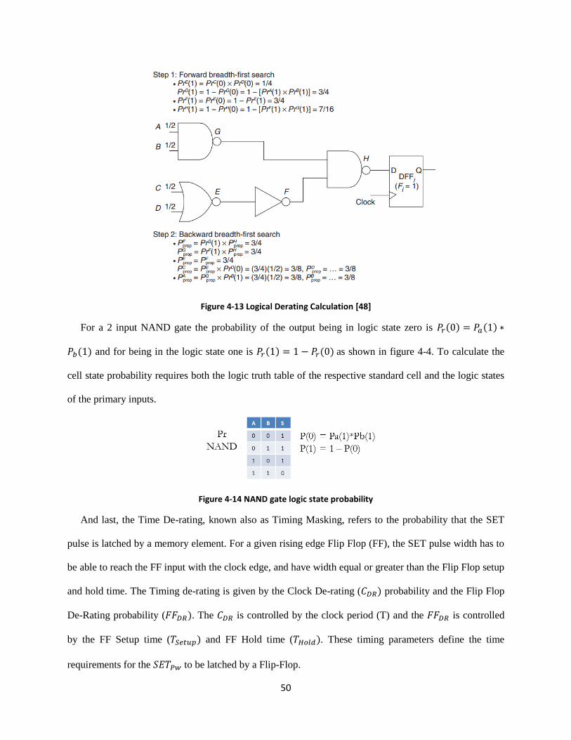
50
Figure 4-13 Logical Derating Calculation [48]
For a 2 input NAND gate the probability of the output being in logic state zero is 𝑃𝑟(0) = 𝑃𝑎(1) ∗
𝑃𝑏(1) and for being in the logic state one is 𝑃𝑟(1) = 1 − 𝑃𝑟(0) as shown in figure 4-4. To calculate the
cell state probability requires both the logic truth table of the respective standard cell and the logic states
of the primary inputs.
Figure 4-14 NAND gate logic state probability
And last, the Time De-rating, known also as Timing Masking, refers to the probability that the SET
pulse is latched by a memory element. For a given rising edge Flip Flop (FF), the SET pulse width has to
be able to reach the FF input with the clock edge, and have width equal or greater than the Flip Flop setup
and hold time. The Timing de-rating is given by the Clock De-rating (𝐶𝐷𝑅) probability and the Flip Flop
De-Rating probability (𝐹𝐹𝐷𝑅). The 𝐶𝐷𝑅 is controlled by the clock period (T) and the 𝐹𝐹𝐷𝑅 is controlled
by the FF Setup time (𝑇𝑆𝑒𝑡𝑢𝑝) and FF Hold time (𝑇𝐻𝑜𝑙𝑑). These timing parameters define the time
requirements for the 𝑆𝐸𝑇𝑃𝑤 to be latched by a Flip-Flop.
51
𝐶𝐷𝑅 = 𝑆𝐸𝑇𝑃𝑤
𝑇⁄ 𝑆𝐸𝑇𝑃𝑤 ≤ 𝑇
1 𝑒𝑙𝑠𝑒
𝐹𝐹𝐷𝑅 = 1 𝑆𝐸𝑇𝑃𝑤 ≥ 𝑇𝑆𝑒𝑡𝑢𝑝 + 𝑇𝐻𝑜𝑙𝑑0 𝑒𝑙𝑠𝑒
𝑇𝐷𝑅 = 𝐶𝐷𝑅 ∙ 𝐹𝐹𝐷𝑅 . (4.4)
With the last model discussed in this section, it is possible to develop metrics capable of analyzing the
soft error impact on the whole circuit netlist, and not just for a single node/cell. This is the subject of the
next section.
4.3 Soft Error Sensitivity and Cross Section Estimation
The models discussed in the last section are used to establish the basic framework to analyze the circuit
soft-error cross-section and the circuit soft-error sensitivity index. The soft-error cross-section is the
metric used to analyze the effective number of errors/chip area for a given circuit. The circuit soft-error
sensitivity index is a simpler metric used to estimate the increase/decrease of the severity of the soft error
event for the netlist. Notice that the soft error sensitivity index does not directly translate into a countable
error.
The formulation of the circuit soft-error sensitivity index is shown in equations (4.5 and 4.6). These
equations are a commonly used approach to evaluate the soft-error sensitivity of netlists in high
abstraction models and it was used before by [48, 47]. This work expands the formulation by considering
charge sharing, as shown in the second term of Eqn. 4.6. The circuit soft-error sensitivity index is given
by the summation of individual nodes soft-error sensitivity as given by Eqn. 4.5. The nodal soft-error
sensitivity index is given by the multiplication of the generation probability, electrical, logical and time
de-rating factors.
𝑁𝑆𝑃(𝑖) = 𝐺𝑒𝑛𝑝(𝑖) ∙ 𝐸𝑙𝐷𝑅(𝑖) ∙ 𝐿𝑜𝐷𝑅(𝑖) ∙ 𝑇𝐷𝑅(𝑖) (4.5)
𝐶𝑆𝑃(𝐺) =∑(𝑁𝑆𝑃(𝑖) +∑𝑁𝑆𝑃(𝑗)
𝐾
𝑗=0
)
𝑁
𝑖=0
(4.6)

52
In equation 4.6, for each standard cell evaluated, the neighboring standard cells placed there by the
placement tool are also evaluated. Since their distance from the SEE hit location is known, models
presented in this thesis can be sued to estimate charge collected by them due to charge sharing. This is
performed for both left and right cells of the hit node. A standard cell located above and below the hit cell
is not considered in this computation since these cells are physically located in different regions and
separated by routing channels.
This analysis is useful to quickly analyze the netlist and extract a reference soft-error measurement to
make decisions during the design flow. This is possible because of the linear computational complexity
O(n) of the models developed in this work. However as discussed before, this equation can’t be directly
translated into an error cross-section. For this purpose another metric based on the de-rating factors is
required. Since the main objective here is to mitigate soft error threat, estimation of cross-section can be
performed at the end of the Physical Synthesis.
A novel methodology proposed in [49] and [47] provides guidance to estimate the circuit soft-error
cross-section using probability matrices and fault-injection simulations. In this work, a Monte-Carlo-
based methodology was adapted to remove the required high number of fault injections and it was
expanded to include the charge sharing effect.
The work from [49] differ from other methodologies by analyzing the soft-error event in multiple
clock cycles, and performing fault injection for the propagation analysis. It defines individual node error
probabilities (𝑃𝐶,𝑁𝐸𝑟𝑟𝑜𝑟) with a similar formulation as Eqn. 4.5 but fault injections are performed to analyze
the netlist response to each clock cycle. This in turn results in an error probability matrix as shown in
Figure 4-15, where each row represents a node sensitivity and each column represents the clock cycle of
the respective analysis. An additional vector (𝐴𝑁) is used to hold the nodal sensitivity area information to
estimate the soft-error cross-section of individual nodes.
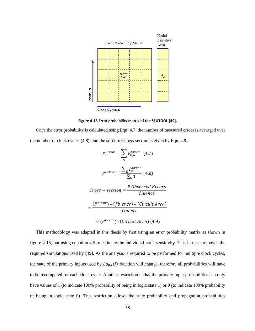
53
Figure 4-15 Error probability matrix of the SEUTOOL [49].
Once the error probability is calculated using Eqn. 4.7, the number of measured errors is averaged over
the number of clock cycles (4.8), and the soft error cross-section is given by Eqn. 4.9.
𝑃𝐶𝐸𝑟𝑟𝑜𝑟 =∑𝑃𝐶,𝑁
𝐸𝑟𝑟𝑜𝑟
𝑁
(4.7)
𝑃𝐸𝑟𝑟𝑜𝑟 =∑ 𝑃𝐶
𝐸𝑟𝑟𝑜𝑟𝐶
∑ 1𝐶 (4.8)
𝐶𝑟𝑜𝑠𝑠 − 𝑠𝑒𝑐𝑡𝑖𝑜𝑛 =# 𝑂𝑏𝑠𝑒𝑟𝑣𝑒𝑑 𝐸𝑟𝑟𝑜𝑟𝑠
𝑓𝑙𝑢𝑒𝑛𝑐𝑒
=(𝑃𝐸𝑟𝑟𝑜𝑟) ∗ (𝑓𝑙𝑢𝑒𝑛𝑐𝑒) ∗ (𝐶𝑖𝑟𝑐𝑢𝑖𝑡 𝐴𝑟𝑒𝑎)
𝑓𝑙𝑢𝑒𝑛𝑐𝑒
= (𝑃𝐸𝑟𝑟𝑜𝑟) ∙ (𝐶𝑖𝑟𝑐𝑢𝑖𝑡 𝐴𝑟𝑒𝑎) (4.9)
This methodology was adapted in this thesis by first using an error probability matrix as shown in
figure 4-15, but using equation 4.5 to estimate the individual node sensitivity. This in turns removes the
required simulations used by [49]. As the analysis is required to be performed for multiple clock cycles,
the state of the primary inputs used by 𝐿𝑜𝐷𝑅(𝑖) function will change, therefore all probabilities will have
to be recomputed for each clock cycle. Another restriction is that the primary input probabilities can only
have values of 1 (to indicate 100% probability of being in logic state 1) or 0 (to indicate 100% probability
of being in logic state 0). This restriction allows the state probability and propagation probabilities
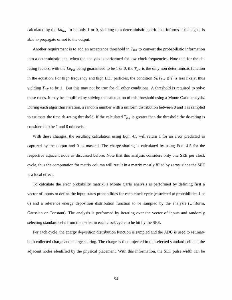
54
calculated by the 𝐿𝑜𝐷𝑅 to be only 1 or 0, yielding to a deterministic metric that informs if the signal is
able to propagate or not to the output.
Another requirement is to add an acceptance threshold in 𝑇𝐷𝑅 to convert the probabilistic information
into a deterministic one, when the analysis is performed for low clock frequencies. Note that for the de-
rating factors, with the 𝐿𝑜𝐷𝑅 being guaranteed to be 1 or 0, the 𝑇𝐷𝑅 is the only non deterministic function
in the equation. For high frequency and high LET particles, the condition 𝑆𝐸𝑇𝑃𝑤 ≤ 𝑇 is less likely, thus
yielding 𝑇𝐷𝑅 to be 1. But this may not be true for all other conditions. A threshold is required to solve
these cases. It may be simplified by solving the calculation of this threshold using a Monte Carlo analysis.
During each algorithm iteration, a random number with a uniform distribution between 0 and 1 is sampled
to estimate the time de-rating threshold. If the calculated 𝑇𝐷𝑅 is greater than the threshold the de-rating is
considered to be 1 and 0 otherwise.
With these changes, the resulting calculation using Eqn. 4.5 will return 1 for an error predicted as
captured by the output and 0 as masked. The charge-sharing is calculated by using Eqn. 4.5 for the
respective adjacent node as discussed before. Note that this analysis considers only one SEE per clock
cycle, thus the computation for matrix column will result in a matrix mostly filled by zeros, since the SEE
is a local effect.
To calculate the error probability matrix, a Monte Carlo analysis is performed by defining first a
vector of inputs to define the input states probabilities for each clock cycle (restricted to probabilities 1 or
0) and a reference energy deposition distribution function to be sampled by the analysis (Uniform,
Gaussian or Constant). The analysis is performed by iterating over the vector of inputs and randomly
selecting standard cells from the netlist in each clock cycle to be hit by the SEE.
For each cycle, the energy deposition distribution function is sampled and the ADC is used to estimate
both collected charge and charge sharing. The charge is then injected in the selected standard cell and the
adjacent nodes identified by the physical placement. With this information, the SET pulse width can be
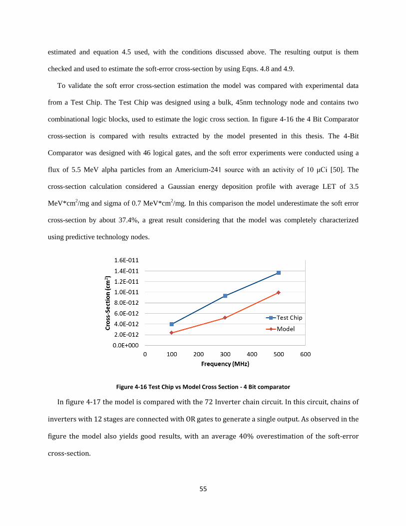
55
estimated and equation 4.5 used, with the conditions discussed above. The resulting output is them
checked and used to estimate the soft-error cross-section by using Eqns. 4.8 and 4.9.
To validate the soft error cross-section estimation the model was compared with experimental data
from a Test Chip. The Test Chip was designed using a bulk, 45nm technology node and contains two
combinational logic blocks, used to estimate the logic cross section. In figure 4-16 the 4 Bit Comparator
cross-section is compared with results extracted by the model presented in this thesis. The 4-Bit
Comparator was designed with 46 logical gates, and the soft error experiments were conducted using a
flux of 5.5 MeV alpha particles from an Americium-241 source with an activity of 10 μCi [50]. The
cross-section calculation considered a Gaussian energy deposition profile with average LET of 3.5
MeV*cm2/mg and sigma of 0.7 MeV*cm
2/mg. In this comparison the model underestimate the soft error
cross-section by about 37.4%, a great result considering that the model was completely characterized
using predictive technology nodes.
Figure 4-16 Test Chip vs Model Cross Section - 4 Bit comparator
In figure 4-17 the model is compared with the 72 Inverter chain circuit. In this circuit, chains of
inverters with 12 stages are connected with OR gates to generate a single output. As observed in the
figure the model also yields good results, with an average 40% overestimation of the soft-error
cross-section.
56
Figure 4-17 Test Chip vs Model Cross Section - 72 Inverter chain
These results show that the model is able to estimate the soft error cross-section with
considerable accuracy. It is also important to indicate that the methodology was properly able to
model the impact of the frequency variation, by correctly predicting the increase in soft error cross-
section with the frequency increase.
4.4 Circuit Analysis Conclusions
Two metrics to evaluate the circuit response to SEE were presented and discussed, and will be used to
report the soft error data in this work. With the framework to analyze soft errors for both standard cells
and circuits developed, the focus now is on the Physical Synthesis process.
.
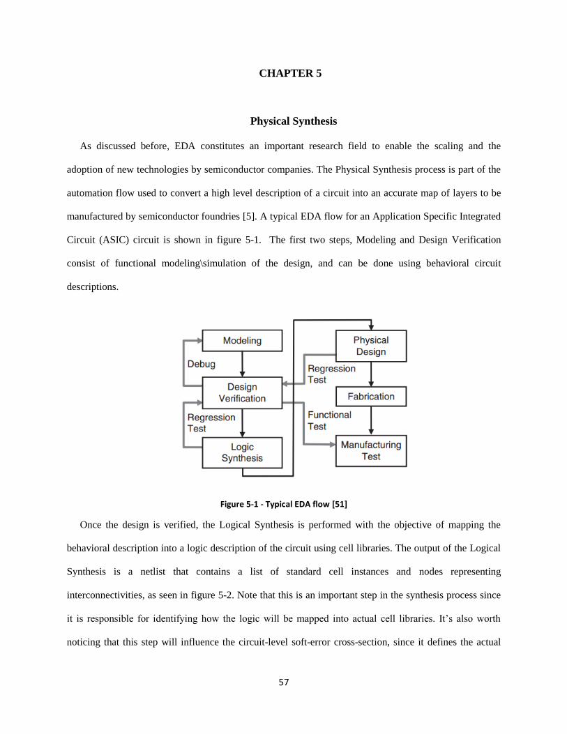
57
CHAPTER 5
5. Physical Synthesis
As discussed before, EDA constitutes an important research field to enable the scaling and the
adoption of new technologies by semiconductor companies. The Physical Synthesis process is part of the
automation flow used to convert a high level description of a circuit into an accurate map of layers to be
manufactured by semiconductor foundries [5]. A typical EDA flow for an Application Specific Integrated
Circuit (ASIC) circuit is shown in figure 5-1. The first two steps, Modeling and Design Verification
consist of functional modeling\simulation of the design, and can be done using behavioral circuit
descriptions.
Figure 5-1 - Typical EDA flow [51]
Once the design is verified, the Logical Synthesis is performed with the objective of mapping the
behavioral description into a logic description of the circuit using cell libraries. The output of the Logical
Synthesis is a netlist that contains a list of standard cell instances and nodes representing
interconnectivities, as seen in figure 5-2. Note that this is an important step in the synthesis process since
it is responsible for identifying how the logic will be mapped into actual cell libraries. It’s also worth
noticing that this step will influence the circuit-level soft-error cross-section, since it defines the actual
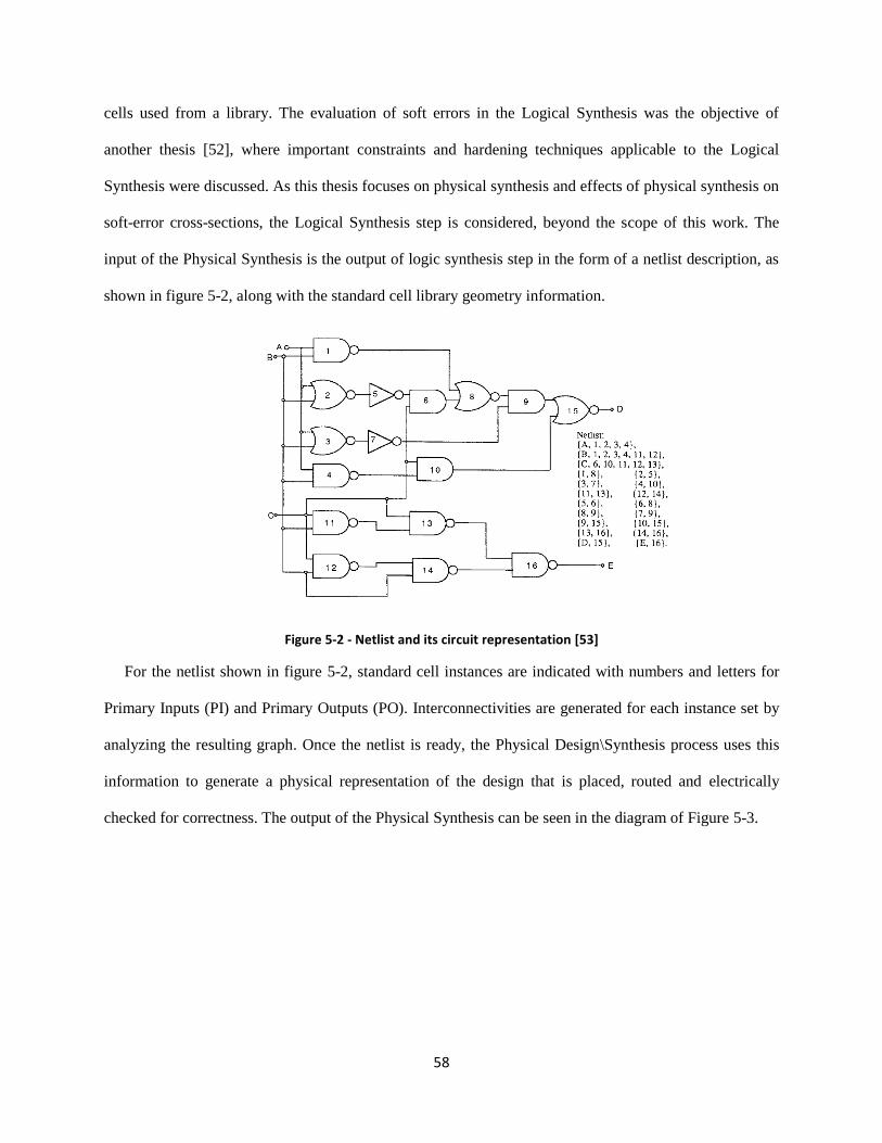
58
cells used from a library. The evaluation of soft errors in the Logical Synthesis was the objective of
another thesis [52], where important constraints and hardening techniques applicable to the Logical
Synthesis were discussed. As this thesis focuses on physical synthesis and effects of physical synthesis on
soft-error cross-sections, the Logical Synthesis step is considered, beyond the scope of this work. The
input of the Physical Synthesis is the output of logic synthesis step in the form of a netlist description, as
shown in figure 5-2, along with the standard cell library geometry information.
Figure 5-2 - Netlist and its circuit representation [53]
For the netlist shown in figure 5-2, standard cell instances are indicated with numbers and letters for
Primary Inputs (PI) and Primary Outputs (PO). Interconnectivities are generated for each instance set by
analyzing the resulting graph. Once the netlist is ready, the Physical Design\Synthesis process uses this
information to generate a physical representation of the design that is placed, routed and electrically
checked for correctness. The output of the Physical Synthesis can be seen in the diagram of Figure 5-3.
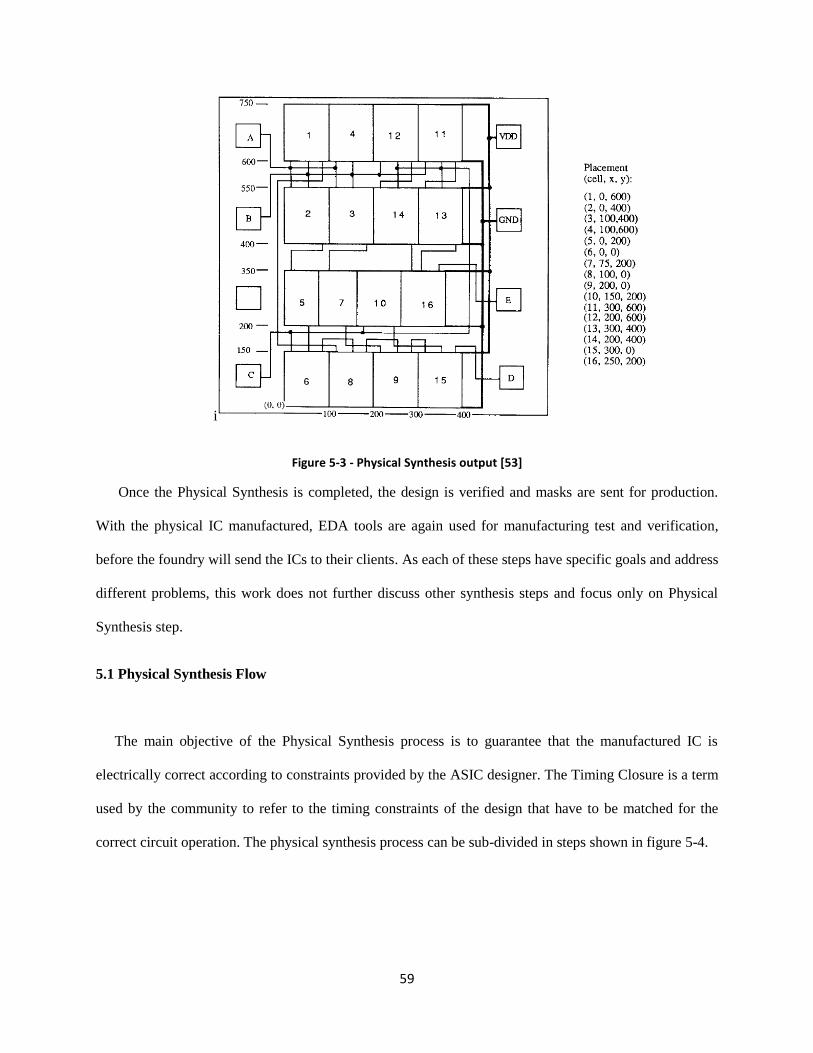
59
i
Figure 5-3 - Physical Synthesis output [53]
Once the Physical Synthesis is completed, the design is verified and masks are sent for production.
With the physical IC manufactured, EDA tools are again used for manufacturing test and verification,
before the foundry will send the ICs to their clients. As each of these steps have specific goals and address
different problems, this work does not further discuss other synthesis steps and focus only on Physical
Synthesis step.
5.1 Physical Synthesis Flow
The main objective of the Physical Synthesis process is to guarantee that the manufactured IC is
electrically correct according to constraints provided by the ASIC designer. The Timing Closure is a term
used by the community to refer to the timing constraints of the design that have to be matched for the
correct circuit operation. The physical synthesis process can be sub-divided in steps shown in figure 5-4.
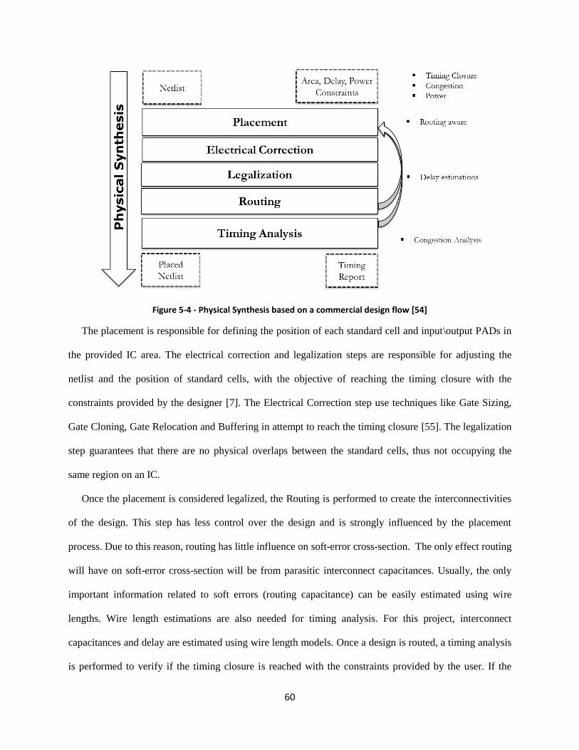
60
Figure 5-4 - Physical Synthesis based on a commercial design flow [54]
The placement is responsible for defining the position of each standard cell and input\output PADs in
the provided IC area. The electrical correction and legalization steps are responsible for adjusting the
netlist and the position of standard cells, with the objective of reaching the timing closure with the
constraints provided by the designer [7]. The Electrical Correction step use techniques like Gate Sizing,
Gate Cloning, Gate Relocation and Buffering in attempt to reach the timing closure [55]. The legalization
step guarantees that there are no physical overlaps between the standard cells, thus not occupying the
same region on an IC.
Once the placement is considered legalized, the Routing is performed to create the interconnectivities
of the design. This step has less control over the design and is strongly influenced by the placement
process. Due to this reason, routing has little influence on soft-error cross-section. The only effect routing
will have on soft-error cross-section will be from parasitic interconnect capacitances. Usually, the only
important information related to soft errors (routing capacitance) can be easily estimated using wire
lengths. Wire length estimations are also needed for timing analysis. For this project, interconnect
capacitances and delay are estimated using wire length models. Once a design is routed, a timing analysis
is performed to verify if the timing closure is reached with the constraints provided by the user. If the
61
design does not reach the timing closure, the design has to be re-placed, re-routed, and passed through the
electrical correction step again.
The electrical correction techniques do influence the electrical characteristics of the circuit, and thus
will influence the soft error response of the IC. It’s important to understand the techniques used by EDA
to solve the circuit delay problems and how they will impact the circuit soft error response. A review of
the main electrical correction techniques applied in the Physical Synthesis is discussed next.
5.2 Electrical Correction Techniques and Soft Errors
The main electrical correction techniques used in the Physical Synthesis are the Gate Sizing, Gate
Cloning, Gate Relocation, and Buffering as discussed by [55]. These techniques are commonly used by
the synthesis to achieve the timing closure after the initial netlist placement is available.
The Gate Sizing technique [56] consists of replacing standard cells that are not able to drive the
expected load (higher load capacitances than expected), with a cell with identical function but higher
current driving capability. This is shown in figure 5-5. In a standard cell library, higher driving capability
is achieved through adding transistors in parallel to the ones already present in the cell. This operation,
increases the width of the standard cell, but not the cell height. The addition of transistors in parallel
reduces the total resistance from the output to the power rail, thus increasing the cell drive current
(I=V/R). The usage of Gate Sizing as a technique to mitigate Soft Errors was proposed by [57] with an
algorithm to compute the necessary gate size to mitigate SETs modeled by the double exponential
equation [31]. The increased driving-current capability at the output node reduces the SET pulse width at
that node, thereby reducing the circuit soft-error vulnerability. The effectiveness of transistor sizing to
mitigate soft errors was further evaluated by [58] using a TCAD tool for a 90-nm technology.
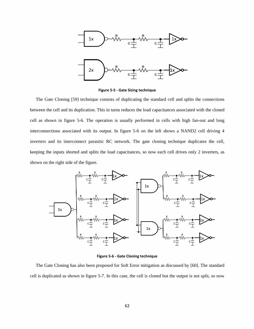
62
Figure 5-5 - Gate Sizing technique
The Gate Cloning [59] technique consists of duplicating the standard cell and splits the connections
between the cell and its duplication. This in turns reduces the load capacitances associated with the cloned
cell as shown in figure 5-6. The operation is usually performed in cells with high fan-out and long
interconnections associated with its output. In figure 5-6 on the left shows a NAND2 cell driving 4
inverters and its interconnect parasitic RC network. The gate cloning technique duplicates the cell,
keeping the inputs shorted and splits the load capacitances, so now each cell drives only 2 inverters, as
shown on the right side of the figure.
Figure 5-6 - Gate Cloning technique
The Gate Cloning has also been proposed for Soft Error mitigation as discussed by [60]. The standard
cell is duplicated as shown in figure 5-7. In this case, the cell is cloned but the output is not split, so now
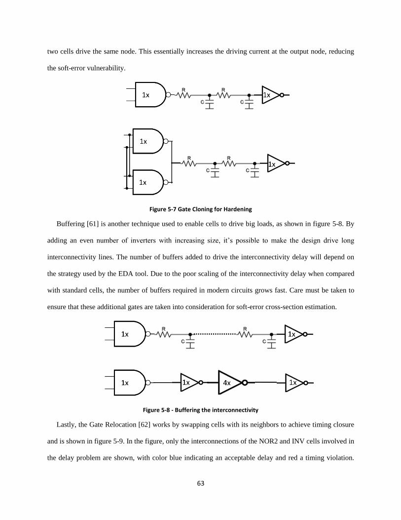
63
two cells drive the same node. This essentially increases the driving current at the output node, reducing
the soft-error vulnerability.
Figure 5-7 Gate Cloning for Hardening
Buffering [61] is another technique used to enable cells to drive big loads, as shown in figure 5-8. By
adding an even number of inverters with increasing size, it’s possible to make the design drive long
interconnectivity lines. The number of buffers added to drive the interconnectivity delay will depend on
the strategy used by the EDA tool. Due to the poor scaling of the interconnectivity delay when compared
with standard cells, the number of buffers required in modern circuits grows fast. Care must be taken to
ensure that these additional gates are taken into consideration for soft-error cross-section estimation.
Figure 5-8 - Buffering the interconnectivity
Lastly, the Gate Relocation [62] works by swapping cells with its neighbors to achieve timing closure
and is shown in figure 5-9. In the figure, only the interconnections of the NOR2 and INV cells involved in
the delay problem are shown, with color blue indicating an acceptable delay and red a timing violation.
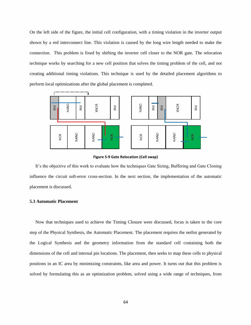
64
On the left side of the figure, the initial cell configuration, with a timing violation in the inverter output
shown by a red interconnect line. This violation is caused by the long wire length needed to make the
connection. This problem is fixed by shifting the inverter cell closer to the NOR gate. The relocation
technique works by searching for a new cell position that solves the timing problem of the cell, and not
creating additional timing violations. This technique is used by the detailed placement algorithms to
perform local optimizations after the global placement is completed.
Figure 5-9 Gate Relocation (Cell swap)
It’s the objective of this work to evaluate how the techniques Gate Sizing, Buffering and Gate Cloning
influence the circuit soft-error cross-section. In the next section, the implementation of the automatic
placement is discussed.
5.3 Automatic Placement
Now that techniques used to achieve the Timing Closure were discussed, focus is taken to the core
step of the Physical Synthesis, the Automatic Placement. The placement requires the netlist generated by
the Logical Synthesis and the geometry information from the standard cell containing both the
dimensions of the cell and internal pin locations. The placement, then seeks to map these cells to physical
positions in an IC area by minimizing constraints, like area and power. It turns out that this problem is
solved by formulating this as an optimization problem, solved using a wide range of techniques, from
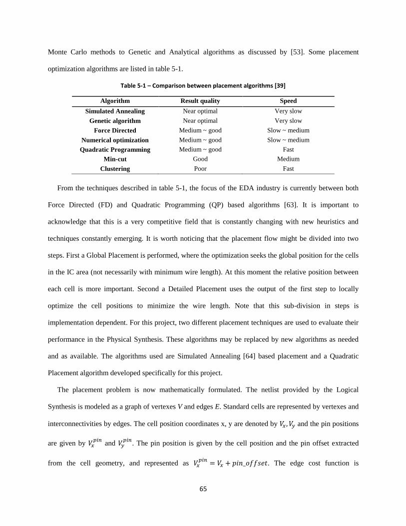
65
Monte Carlo methods to Genetic and Analytical algorithms as discussed by [53]. Some placement
optimization algorithms are listed in table 5-1.
Table 5-1 – Comparison between placement algorithms [39]
Algorithm Result quality Speed
Simulated Annealing Near optimal Very slow
Genetic algorithm Near optimal Very slow
Force Directed Medium ~ good Slow ~ medium
Numerical optimization Medium ~ good Slow ~ medium
Quadratic Programming Medium ~ good Fast
Min-cut Good Medium
Clustering Poor Fast
From the techniques described in table 5-1, the focus of the EDA industry is currently between both
Force Directed (FD) and Quadratic Programming (QP) based algorithms [63]. It is important to
acknowledge that this is a very competitive field that is constantly changing with new heuristics and
techniques constantly emerging. It is worth noticing that the placement flow might be divided into two
steps. First a Global Placement is performed, where the optimization seeks the global position for the cells
in the IC area (not necessarily with minimum wire length). At this moment the relative position between
each cell is more important. Second a Detailed Placement uses the output of the first step to locally
optimize the cell positions to minimize the wire length. Note that this sub-division in steps is
implementation dependent. For this project, two different placement techniques are used to evaluate their
performance in the Physical Synthesis. These algorithms may be replaced by new algorithms as needed
and as available. The algorithms used are Simulated Annealing [64] based placement and a Quadratic
Placement algorithm developed specifically for this project.
The placement problem is now mathematically formulated. The netlist provided by the Logical
Synthesis is modeled as a graph of vertexes V and edges E. Standard cells are represented by vertexes and
interconnectivities by edges. The cell position coordinates x, y are denoted by 𝑉𝑥 , 𝑉𝑦 and the pin positions
are given by 𝑉𝑥𝑝𝑖𝑛
and 𝑉𝑦𝑝𝑖𝑛
. The pin position is given by the cell position and the pin offset extracted
from the cell geometry, and represented as 𝑉𝑥𝑝𝑖𝑛= 𝑉𝑥 + 𝑝𝑖𝑛_𝑜𝑓𝑓𝑠𝑒𝑡. The edge cost function is
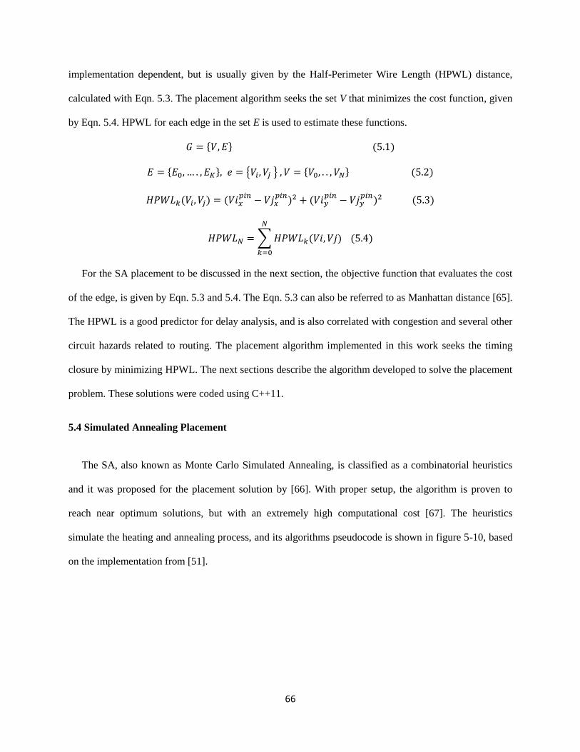
66
implementation dependent, but is usually given by the Half-Perimeter Wire Length (HPWL) distance,
calculated with Eqn. 5.3. The placement algorithm seeks the set V that minimizes the cost function, given
by Eqn. 5.4. HPWL for each edge in the set E is used to estimate these functions.
𝐺 = 𝑉, 𝐸 (5.1)
𝐸 = 𝐸0, … . , 𝐸𝐾, 𝑒 = 𝑉𝑖, 𝑉𝑗 , 𝑉 = 𝑉0, . . , 𝑉𝑁 (5.2)
𝐻𝑃𝑊𝐿𝑘(𝑉𝑖, 𝑉𝑗) = (𝑉𝑖𝑥𝑝𝑖𝑛− 𝑉𝑗𝑥
𝑝𝑖𝑛)2 + (𝑉𝑖𝑦
𝑝𝑖𝑛− 𝑉𝑗𝑦
𝑝𝑖𝑛)2 (5.3)
𝐻𝑃𝑊𝐿𝑁 =∑𝐻𝑃𝑊𝐿𝑘(𝑉𝑖, 𝑉𝑗)
𝑁
𝑘=0
(5.4)
For the SA placement to be discussed in the next section, the objective function that evaluates the cost
of the edge, is given by Eqn. 5.3 and 5.4. The Eqn. 5.3 can also be referred to as Manhattan distance [65].
The HPWL is a good predictor for delay analysis, and is also correlated with congestion and several other
circuit hazards related to routing. The placement algorithm implemented in this work seeks the timing
closure by minimizing HPWL. The next sections describe the algorithm developed to solve the placement
problem. These solutions were coded using C++11.
5.4 Simulated Annealing Placement
The SA, also known as Monte Carlo Simulated Annealing, is classified as a combinatorial heuristics
and it was proposed for the placement solution by [66]. With proper setup, the algorithm is proven to
reach near optimum solutions, but with an extremely high computational cost [67]. The heuristics
simulate the heating and annealing process, and its algorithms pseudocode is shown in figure 5-10, based
on the implementation from [51].
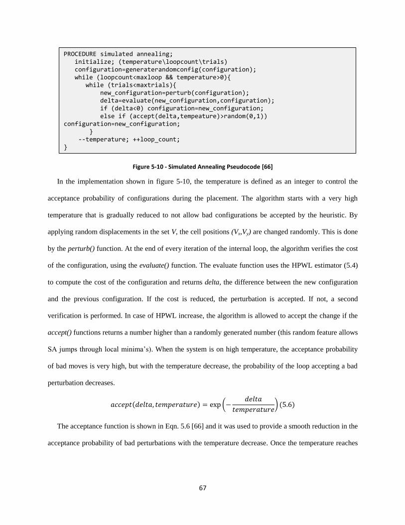
67
Figure 5-10 - Simulated Annealing Pseudocode [66]
In the implementation shown in figure 5-10, the temperature is defined as an integer to control the
acceptance probability of configurations during the placement. The algorithm starts with a very high
temperature that is gradually reduced to not allow bad configurations be accepted by the heuristic. By
applying random displacements in the set V, the cell positions (Vx,Vy) are changed randomly. This is done
by the perturb() function. At the end of every iteration of the internal loop, the algorithm verifies the cost
of the configuration, using the evaluate() function. The evaluate function uses the HPWL estimator (5.4)
to compute the cost of the configuration and returns delta, the difference between the new configuration
and the previous configuration. If the cost is reduced, the perturbation is accepted. If not, a second
verification is performed. In case of HPWL increase, the algorithm is allowed to accept the change if the
accept() functions returns a number higher than a randomly generated number (this random feature allows
SA jumps through local minima’s). When the system is on high temperature, the acceptance probability
of bad moves is very high, but with the temperature decrease, the probability of the loop accepting a bad
perturbation decreases.
𝑎𝑐𝑐𝑒𝑝𝑡(𝑑𝑒𝑙𝑡𝑎, 𝑡𝑒𝑚𝑝𝑒𝑟𝑎𝑡𝑢𝑟𝑒) = exp (−𝑑𝑒𝑙𝑡𝑎
𝑡𝑒𝑚𝑝𝑒𝑟𝑎𝑡𝑢𝑟𝑒) (5.6)
The acceptance function is shown in Eqn. 5.6 [66] and it was used to provide a smooth reduction in the
acceptance probability of bad perturbations with the temperature decrease. Once the temperature reaches
PROCEDURE simulated annealing;
initialize; (temperature\loopcount\trials)
configuration=generaterandomconfig(configuration); while (loopcount<maxloop && temperature>0)
while (trials<maxtrials)
new_configuration=perturb(configuration);
delta=evaluate(new_configuration,configuration);
if (delta<0) configuration=new_configuration;
else if (accept(delta,tempeature)>random(0,1)) configuration=new_configuration;
--temperature; ++loop_count;
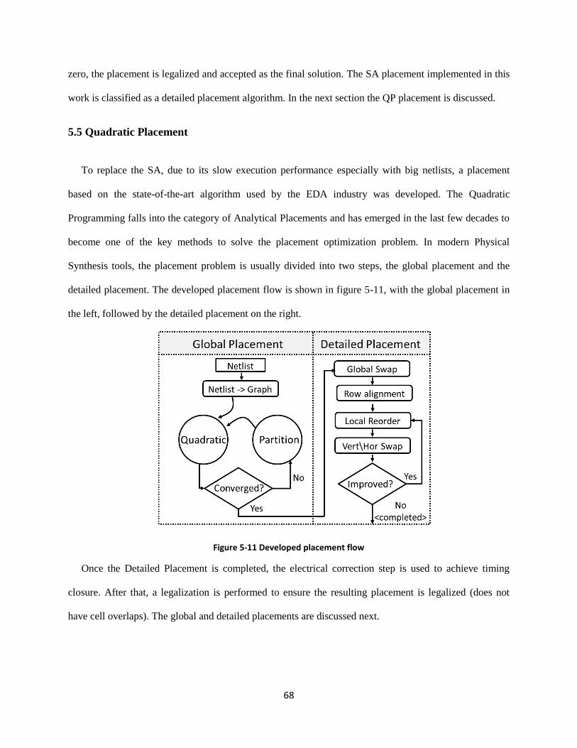
68
zero, the placement is legalized and accepted as the final solution. The SA placement implemented in this
work is classified as a detailed placement algorithm. In the next section the QP placement is discussed.
5.5 Quadratic Placement
To replace the SA, due to its slow execution performance especially with big netlists, a placement
based on the state-of-the-art algorithm used by the EDA industry was developed. The Quadratic
Programming falls into the category of Analytical Placements and has emerged in the last few decades to
become one of the key methods to solve the placement optimization problem. In modern Physical
Synthesis tools, the placement problem is usually divided into two steps, the global placement and the
detailed placement. The developed placement flow is shown in figure 5-11, with the global placement in
the left, followed by the detailed placement on the right.
Figure 5-11 Developed placement flow
Once the Detailed Placement is completed, the electrical correction step is used to achieve timing
closure. After that, a legalization is performed to ensure the resulting placement is legalized (does not
have cell overlaps). The global and detailed placements are discussed next.
69
5.5.1 Global Placement
The global placement, as shown in figure 5-11, uses Quadratic Programming to solve the
optimization problem discussed in section 5.3. In this work the Quadratic Placement uses the region
partition algorithm to reduce the overlap between cells and spread of cells in the placement area [68]. In
the QP implemented in this work, the length of the netlist is given by the quadratic cost function (shown
in Eqn. 5.7) where the 𝑤𝑥,𝑝𝑞 and 𝑤𝑦,𝑝𝑞 are the Bound2Bound weight factor [69] used to take into account
pin density when estimating the optimum wire length, and is given by Eqn. 5.8. The equations ahead are
based on the implementation of both [68] and [69].
𝛤 =1
2∑ 𝑤𝑥,𝑖𝑗(𝑉𝑖𝑥
𝑝𝑖𝑛+ 𝑉𝑗𝑥
𝑝𝑖𝑛)2
𝐾
𝑒=(𝑉𝑖,𝑉𝑗)𝜖𝐸
+𝑤𝑦,𝑖𝑗(𝑉𝑖𝑦𝑝𝑖𝑛+ 𝑉𝑗𝑦
𝑝𝑖𝑛)2 (5.7)
𝑤𝑥,𝑖𝑗 =
0, 𝑖𝑓 𝑖 𝑎𝑛𝑑 𝑗 𝑎𝑟𝑒 𝑖𝑛𝑛𝑒𝑟 𝑝𝑖𝑛𝑠2
𝑝 − 1∙
1
|𝑉𝑖𝑥𝑝𝑖𝑛− 𝑉𝑗𝑥
𝑝𝑖𝑛|, 𝑒𝑙𝑠𝑒 (5.8)
To minimize the quadratic function 𝛤, Eqn. (5.7) is transformed in a matrix vector notation as
shown in Eqn. 5.10, where x and y are the vector position of the M movable blocks (Eqn. 5.9), and
vectors dx and dy are used to reflect the connections between fixed modules and movable blocks [68].The
matrices Cx and Cy are the connectivity matrices of dimension M x M and represent the connectivity
between movable blocks. The generation of these matrixes is performed using the method proposed by
[69].
𝒙 = (𝑉𝑥0, … . , 𝑉𝑥𝑀)𝑇 𝒚 = (𝑉𝑦0, … . , 𝑉𝑦𝑀)
𝑇 (5.9)
𝛤 =1
2𝒙𝑇𝑪𝑥𝒙 + 𝒙
𝑇𝒅𝑥 +1
2𝒚𝑇𝑪𝑦𝒚 + 𝒚
𝑇𝒅𝑦 (5.10)
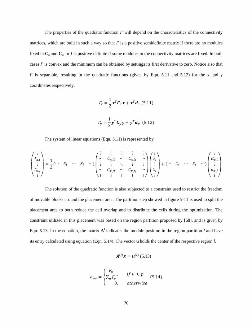
70
The properties of the quadratic function 𝛤 will depend on the characteristics of the connectivity
matrices, which are built in such a way so that 𝛤 is a positive semidefinite matrix if there are no modules
fixed in Cx and Cy, or 𝛤is positive definite if some modules in the connectivity matrices are fixed. In both
cases 𝛤 is convex and the minimum can be obtained by settings its first derivative to zero. Notice also that
𝛤 is separable, resulting in the quadratic functions (given by Eqn. 5.11 and 5.12) for the x and y
coordinates respectively.
𝛤𝑥 =1
2𝒙𝑇𝑪𝑥𝒙 + 𝒙
𝑇𝒅𝑥 (5.11)
𝛤𝑦 =1
2𝒚𝑇𝑪𝑦𝒚 + 𝒚
𝑇𝒅𝑦 (5.12)
The system of linear equations (Eqn. 5.11) is represented by
(
⋮𝛤𝑥,𝑖⋮𝛤𝑥,𝑗⋮ )
=1
2(⋯ 𝑥𝑖 ⋯ 𝑥𝑗 ⋯)
(
⋮ ⋮ ⋮ ⋮ ⋮⋯ 𝐶𝑥,𝑖𝑖 ⋯ 𝐶𝑥,𝑖𝑗 ⋯
⋮ ⋮ ⋱ ⋮ ⋮⋯ 𝐶𝑥,𝑗𝑖 ⋯ 𝐶𝑥,𝑗𝑗 ⋯
⋮ ⋮ ⋮ ⋮ ⋮ )
(
⋮𝑥𝑖⋮𝑥𝑗⋮ )
+ (⋯ 𝑥𝑖 ⋯ 𝑥𝑗 ⋯)
(
⋮𝑑𝑥,𝑖⋮𝑑𝑥,𝑗⋮ )
The solution of the quadratic function is also subjected to a constraint used to restrict the freedom
of movable blocks around the placement area. The partition step showed in figure 5-11 is used to split the
placement area to both reduce the cell overlap and to distribute the cells during the optimization. The
constraint utilized in this placement was based on the region partition proposed by [68], and is given by
Eqn. 5.13. In the equation, the matrix Al indicates the module position in the region partition l and have
its entry calculated using equation (Eqn. 5.14). The vector u holds the center of the respective region l.
𝑨(𝑙)𝒙 = 𝒖(𝑙) (5.13)
𝑎𝑝𝑢 =
𝐹𝑢∑ 𝐹𝑦𝑢
, 𝑖𝑓 𝑢 ∈ 𝑝
0, 𝑜𝑡ℎ𝑒𝑟𝑤𝑖𝑠𝑒
(5.14)

71
In Eqn. 5.14, 𝐹𝑢 is the total unit area occupied by module u and p is the region. The constraint,
given by Eqn. 5.13, has the effect of restricting the modules in the matrix 𝑨(𝑙) to the respective regions
indicated by the vector 𝒖(𝑙). The central coordinates of each region partition act like a gravity pulling
modules away from the initial configuration, reducing the amount of overlap between the cells. The
matrix 𝑨(𝑙) has M columns and L lines for each region partition. As a consequence to the fact that a
module can’t be in more them one region, each column in the matrix contains only one nonzero entry, as
indicated by Eqn. 5.14. With both constraint and objective function stated, the minimization problem can
be formulated as Eqn. 5.15.
𝑚𝑖𝑛𝑥∈𝑀 = 1
2𝒙𝑇𝑪𝑥𝒙 + 𝒙
𝑇𝒅𝑥 |𝑨(𝑙)𝒙 = 𝒖(𝑙) (5.15)
As discussed before, the 𝛤 is positive-definite and convex. To solve Eqn. 5.15, the library
QuadProg++ [70] is used in this work. The library solves the QP by implementing the Goldfarb-Idnani
active-set dual method presented by [71] to solve strictly convex problems. With the resulting cell
configuration, the placement evaluates the placement convergence seeking high density overlaps. If there
are still areas in the placement with high density cell overlaps, the region is further partitioned. In every
high overlapping area, the algorithm makes a new region partition and call QP iteratively. The addition of
a new partition increases the size of 𝑨(𝑙) by one. Once the convergence is reached, the detailed placement
process is started.
5.5.2 Detailed Placement
Once the Global Placement is completed, an optimization step is performed to fix bad cell
positions generated by the region-partition algorithm discussed in the last section. During the global
placement, when a region partition is defined, cells are pulled to the region central location and will not
be able to return to the previous partition. In some cases, groups of connected cells are split in different
regions when they shouldn’t be split. To achieve a better cell organization, the Global Swap step is used
72
in the detailed placement to move cells freely in the placement area. During the detailed placement
process, the region partition is ignored.
The Global Swap is performed once, by iterating over the M movable cells seeking for the
optimum cell position (𝑥𝑜𝑝𝑡 , 𝑦𝑜𝑝𝑡) given the current placement condition. The estimated optimum cell
position [72] is given by the median of the x and y coordinates of each cell neighbors (given by Eqn.
5.15-5.16).
𝑥𝑜𝑝𝑡 = 𝑚𝑒𝑑𝑖𝑎𝑛(𝑥0, 𝑥1, … . , 𝑥ℎ) (5.15)
𝑦𝑜𝑝𝑡 = 𝑚𝑒𝑑𝑖𝑎𝑛(𝑦0, 𝑦1, … . , 𝑦ℎ) (5.16)
After the 𝑥𝑜𝑝𝑡 , 𝑦𝑜𝑝𝑡 are calculated, the HPWL method is used to determine if there is an
improvement over the wire length. If the netlist is improved, the cell position is updated and the algorithm
continues until all cells are verified. With the Global Swap completed, the Row Alignment is started.
The resulting placement now has cells spread around the placement area and overlaps between
cells exist. To remove the overlap and put the cells in a row organization (also adding routing channel),
the algorithm uses the method proposed by [68] to align the modules without perturbing the relative
organization between the cells. The Row Alignment step consists of first ordering the cells by the y
coordination. Once the order along the y-direction is completed, an estimation is calculated to determine
the number of cells per row to define sub-sets to be placed in each row. Once this sub-set is defined, the
cells are now ordered by their x-coordinates and placed in their positions within each row. In this thesis,
the cell ordering is performed using the Merge Sort algorithm [73], with worst case performance of O(n
log n). At the end of this step, the cells are organized in rows separated by routing channels (with channel
height defined by the user).
With the cells organized in rows, a local optimization step is performed to relocate bad placement
of individual cells and to improve the netlist wire length. The algorithm starts a loop that stops when no
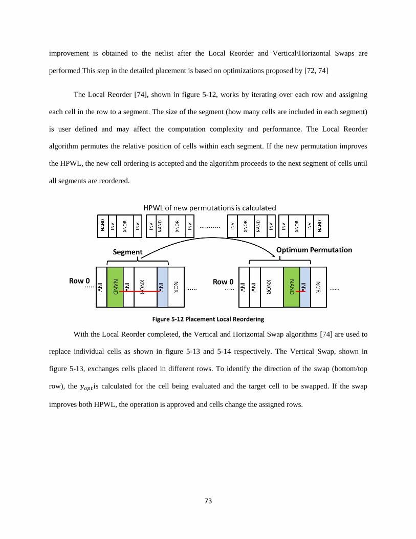
73
improvement is obtained to the netlist after the Local Reorder and Vertical\Horizontal Swaps are
performed This step in the detailed placement is based on optimizations proposed by [72, 74]
The Local Reorder [74], shown in figure 5-12, works by iterating over each row and assigning
each cell in the row to a segment. The size of the segment (how many cells are included in each segment)
is user defined and may affect the computation complexity and performance. The Local Reorder
algorithm permutes the relative position of cells within each segment. If the new permutation improves
the HPWL, the new cell ordering is accepted and the algorithm proceeds to the next segment of cells until
all segments are reordered.
Figure 5-12 Placement Local Reordering
With the Local Reorder completed, the Vertical and Horizontal Swap algorithms [74] are used to
replace individual cells as shown in figure 5-13 and 5-14 respectively. The Vertical Swap, shown in
figure 5-13, exchanges cells placed in different rows. To identify the direction of the swap (bottom/top
row), the 𝑦𝑜𝑝𝑡is calculated for the cell being evaluated and the target cell to be swapped. If the swap
improves both HPWL, the operation is approved and cells change the assigned rows.
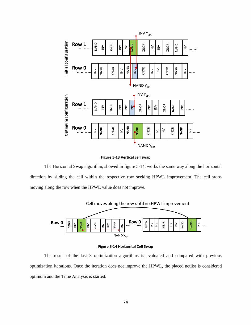
74
Figure 5-13 Vertical cell swap
The Horizontal Swap algorithm, showed in figure 5-14, works the same way along the horizontal
direction by sliding the cell within the respective row seeking HPWL improvement. The cell stops
moving along the row when the HPWL value does not improve.
Figure 5-14 Horizontal Cell Swap
The result of the last 3 optimization algorithms is evaluated and compared with previous
optimization iterations. Once the iteration does not improve the HPWL, the placed netlist is considered
optimum and the Time Analysis is started.
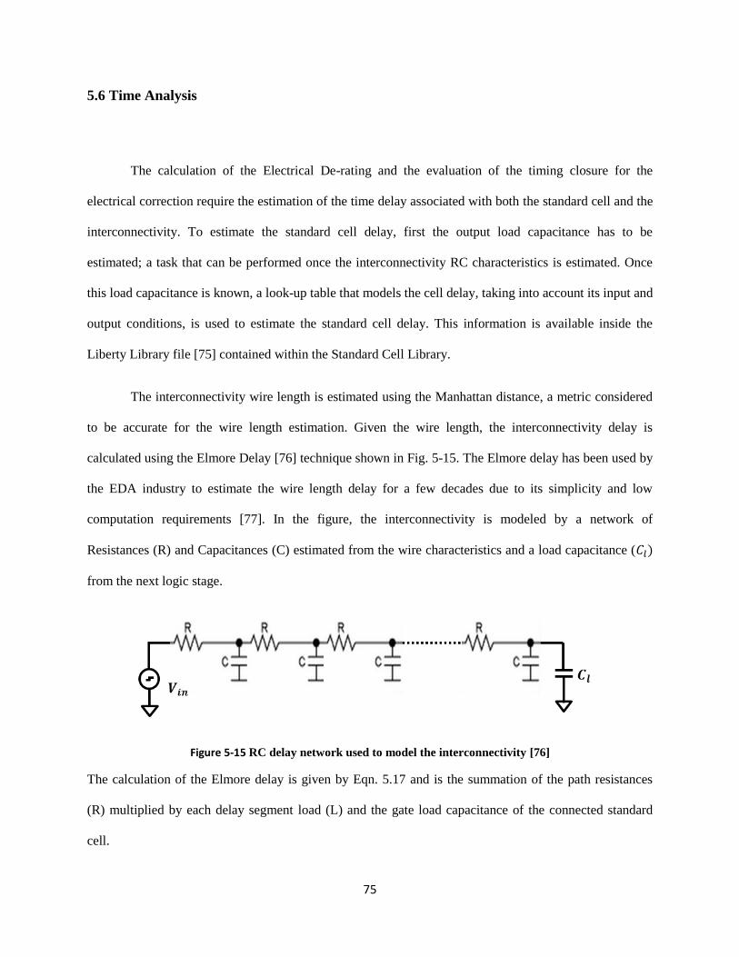
75
5.6 Time Analysis
The calculation of the Electrical De-rating and the evaluation of the timing closure for the
electrical correction require the estimation of the time delay associated with both the standard cell and the
interconnectivity. To estimate the standard cell delay, first the output load capacitance has to be
estimated; a task that can be performed once the interconnectivity RC characteristics is estimated. Once
this load capacitance is known, a look-up table that models the cell delay, taking into account its input and
output conditions, is used to estimate the standard cell delay. This information is available inside the
Liberty Library file [75] contained within the Standard Cell Library.
The interconnectivity wire length is estimated using the Manhattan distance, a metric considered
to be accurate for the wire length estimation. Given the wire length, the interconnectivity delay is
calculated using the Elmore Delay [76] technique shown in Fig. 5-15. The Elmore delay has been used by
the EDA industry to estimate the wire length delay for a few decades due to its simplicity and low
computation requirements [77]. In the figure, the interconnectivity is modeled by a network of
Resistances (R) and Capacitances (C) estimated from the wire characteristics and a load capacitance (𝐶𝑙)
from the next logic stage.
Figure 5-15 RC delay network used to model the interconnectivity [76]
The calculation of the Elmore delay is given by Eqn. 5.17 and is the summation of the path resistances
(R) multiplied by each delay segment load (L) and the gate load capacitance of the connected standard
cell.
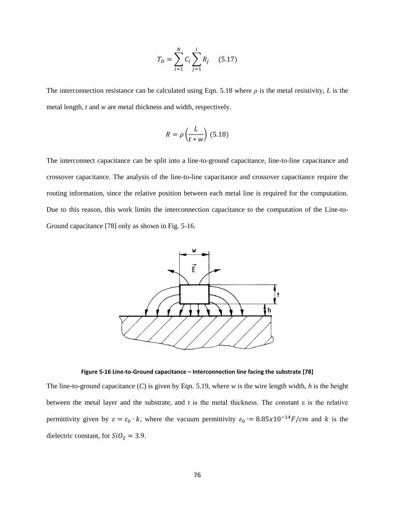
76
𝑇𝐷 =∑𝐶𝑖
𝑁
𝑖=1
∑𝑅𝑗
𝑖
𝑗=1
(5.17)
The interconnection resistance can be calculated using Eqn. 5.18 where ρ is the metal resistivity, L is the
metal length, t and w are metal thickness and width, respectively.
𝑅 = 𝜌 (𝐿
𝑡 ∗ 𝑤) (5.18)
The interconnect capacitance can be split into a line-to-ground capacitance, line-to-line capacitance and
crossover capacitance. The analysis of the line-to-line capacitance and crossover capacitance require the
routing information, since the relative position between each metal line is required for the computation.
Due to this reason, this work limits the interconnection capacitance to the computation of the Line-to-
Ground capacitance [78] only as shown in Fig. 5-16.
Figure 5-16 Line-to-Ground capacitance – Interconnection line facing the substrate [78]
The line-to-ground capacitance (C) is given by Eqn. 5.19, where w is the wire length width, h is the height
between the metal layer and the substrate, and t is the metal thickness. The constant ε is the relative
permittivity given by 𝜀 = 𝜀0 ∙ 𝑘, where the vacuum permittivity 𝜀0 ∙= 8.85𝑥10−14𝐹/𝑐𝑚 and 𝑘 is the
dielectric constant, for 𝑆𝑖𝑂2 = 3.9.
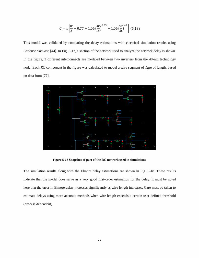
77
𝐶 = 𝜀 [𝑤
ℎ+ 0.77 + 1.06 (
𝑤
ℎ)0.25
+ 1.06 (𝑡
ℎ)0.5
] (5.19)
This model was validated by comparing the delay estimations with electrical simulation results using
Cadence Virtuoso [44]. In Fig. 5-17, a section of the network used to analyze the network delay is shown.
In the figure, 3 different interconnects are modeled between two inverters from the 40-nm technology
node. Each RC component in the figure was calculated to model a wire segment of 1µm of length, based
on data from [77].
Figure 5-17 Snapshot of part of the RC network used in simulations
The simulation results along with the Elmore delay estimations are shown in Fig. 5-18. These results
indicate that the model does serve as a very good first-order estimation for the delay. It must be noted
here that the error in Elmore delay increases significantly as wire length increases. Care must be taken to
estimate delays using more accurate methods when wire length exceeds a certain user-defined threshold
(process dependent).
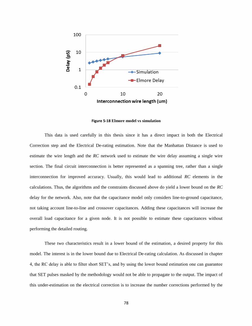
78
Figure 5-18 Elmore model vs simulation
This data is used carefully in this thesis since it has a direct impact in both the Electrical
Correction step and the Electrical De-rating estimation. Note that the Manhattan Distance is used to
estimate the wire length and the RC network used to estimate the wire delay assuming a single wire
section. The final circuit interconnection is better represented as a spanning tree, rather than a single
interconnection for improved accuracy. Usually, this would lead to additional RC elements in the
calculations. Thus, the algorithms and the constraints discussed above do yield a lower bound on the RC
delay for the network. Also, note that the capacitance model only considers line-to-ground capacitance,
not taking account line-to-line and crossover capacitances. Adding these capacitances will increase the
overall load capacitance for a given node. It is not possible to estimate these capacitances without
performing the detailed routing.
These two characteristics result in a lower bound of the estimation, a desired property for this
model. The interest is in the lower bound due to Electrical De-rating calculation. As discussed in chapter
4, the RC delay is able to filter short SET’s, and by using the lower bound estimation one can guarantee
that SET pulses masked by the methodology would not be able to propagate to the output. The impact of
this under-estimation on the electrical correction is to increase the number corrections performed by the

79
model. However, this does not affect the trend to be observed in the analysis of the SER cross-section
analysis.
5.7 Electrical Correction & Legalization
With the Time Analysis completed, the Electrical Correction techniques can be applied to solve
netlist violations. The placed netlist is now analyzed to verify if the Timing Closure is achieved. In this
work, the Timing Closure is formulated using Eqn. 5.20 and 5.21 from [79]. The Eqn. 5.20 models the
Setup Constraint, and refers to long paths in the netlist. It specifies the amount of time the input data
should be steady before the clock edge of each Flip Flop. In the equation Tcycle is the clock period,
tcritical_path is the longest path in the circuit, tsetup the clock setup time and tskew is the clock skew.
𝑇𝑐𝑦𝑐𝑙𝑒 ≥ 𝑡𝑐𝑟𝑖𝑡𝑖𝑐𝑎𝑙𝑝𝑎𝑡ℎ + 𝑡𝑠𝑒𝑡𝑢𝑝 + 𝑡𝑠𝑘𝑒𝑤 (5.20)
The Eqn. 5.21 models the Hold Constraint and refers to short paths used to indicate the amount of
time the input data should be stable after the clock edge. In the Eqn. 5-21, tcomb_delay is the path delay from
the cell to FF, and thold is the Flip Flop hold time.
𝑡𝑐𝑜𝑚𝑏_𝑑𝑒𝑙𝑎𝑦 ≥ 𝑡ℎ𝑜𝑙𝑑 + 𝑡𝑠𝑘𝑒𝑤 (5.21)
The Time Analysis section discussed before is used to provide the timing information required in
this section. The worst and the best case delay paths associated with each node in the graph is stored to
evaluate conditions (given by Eqn. 5.20 and 5.21. If time closure is not achieved (equalities specified in
Eqn. 5-20 and 5-21 are not satisfied), the electrical correction techniques, such as Gate Sizing, Gate
Cloning and Buffering are used to adjust the netlist timing. Because we are also interested in analyzing
the effects of each of these individual techniques, algorithms used in this work allow the user to block the
use of each of these electrical correction techniques. Notice also that the input frequency provided by the
user will have a strong influence on the Timing Closure and will directly impact the number of operations
to be performed in this step.
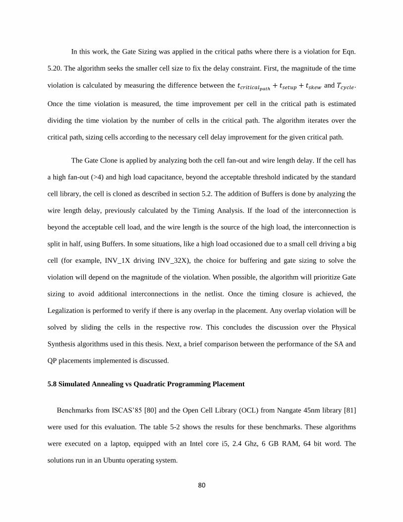
80
In this work, the Gate Sizing was applied in the critical paths where there is a violation for Eqn.
5.20. The algorithm seeks the smaller cell size to fix the delay constraint. First, the magnitude of the time
violation is calculated by measuring the difference between the 𝑡𝑐𝑟𝑖𝑡𝑖𝑐𝑎𝑙𝑝𝑎𝑡ℎ + 𝑡𝑠𝑒𝑡𝑢𝑝 + 𝑡𝑠𝑘𝑒𝑤 and 𝑇𝑐𝑦𝑐𝑙𝑒.
Once the time violation is measured, the time improvement per cell in the critical path is estimated
dividing the time violation by the number of cells in the critical path. The algorithm iterates over the
critical path, sizing cells according to the necessary cell delay improvement for the given critical path.
The Gate Clone is applied by analyzing both the cell fan-out and wire length delay. If the cell has
a high fan-out (>4) and high load capacitance, beyond the acceptable threshold indicated by the standard
cell library, the cell is cloned as described in section 5.2. The addition of Buffers is done by analyzing the
wire length delay, previously calculated by the Timing Analysis. If the load of the interconnection is
beyond the acceptable cell load, and the wire length is the source of the high load, the interconnection is
split in half, using Buffers. In some situations, like a high load occasioned due to a small cell driving a big
cell (for example, INV_1X driving INV_32X), the choice for buffering and gate sizing to solve the
violation will depend on the magnitude of the violation. When possible, the algorithm will prioritize Gate
sizing to avoid additional interconnections in the netlist. Once the timing closure is achieved, the
Legalization is performed to verify if there is any overlap in the placement. Any overlap violation will be
solved by sliding the cells in the respective row. This concludes the discussion over the Physical
Synthesis algorithms used in this thesis. Next, a brief comparison between the performance of the SA and
QP placements implemented is discussed.
5.8 Simulated Annealing vs Quadratic Programming Placement
Benchmarks from ISCAS’85 [80] and the Open Cell Library (OCL) from Nangate 45nm library [81]
were used for this evaluation. The table 5-2 shows the results for these benchmarks. These algorithms
were executed on a laptop, equipped with an Intel core i5, 2.4 Ghz, 6 GB RAM, 64 bit word. The
solutions run in an Ubuntu operating system.
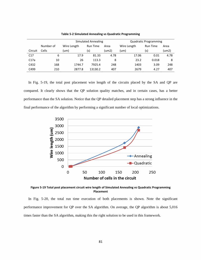
81
Table 5-2 Simulated Annealing vs Quadratic Programming
Simulated Annealing Quadratic Programming
Circuit
Number of
Cells
Wire Length
(um)
Run Time
(s)
Area
(um2)
Wire Length
(um)
Run Time
(s)
Area
(um2)
C17 6 17.9 81.33 4.78 17.06 0.01 4.78
C17a 10 26 113.3 8 23.2 0.018 8
C432 168 1744.7 7925.4 248 1403 3.09 248
C499 210 2877.8 13130.2 407 2679 4.27 407
In Fig. 5-19, the total post placement wire length of the circuits placed by the SA and QP are
compared. It clearly shows that the QP solution quality matches, and in certain cases, has a better
performance than the SA solution. Notice that the QP detailed placement step has a strong influence in the
final performance of the algorithm by performing a significant number of local optimizations.
Figure 5-19 Total post placement circuit wire length of Simulated Annealing vs Quadratic Programming Placement
In Fig. 5-20, the total run time execution of both placements is shown. Note the significant
performance improvement for QP over the SA algorithm. On average, the QP algorithm is about 5,016
times faster than the SA algorithm, making this the right solution to be used in this framework.
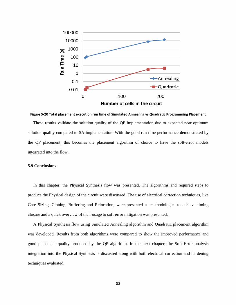
82
Figure 5-20 Total placement execution run time of Simulated Annealing vs Quadratic Programming Placement
These results validate the solution quality of the QP implementation due to expected near optimum
solution quality compared to SA implementation. With the good run-time performance demonstrated by
the QP placement, this becomes the placement algorithm of choice to have the soft-error models
integrated into the flow.
5.9 Conclusions
In this chapter, the Physical Synthesis flow was presented. The algorithms and required steps to
produce the Physical design of the circuit were discussed. The use of electrical correction techniques, like
Gate Sizing, Cloning, Buffering and Relocation, were presented as methodologies to achieve timing
closure and a quick overview of their usage to soft-error mitigation was presented.
A Physical Synthesis flow using Simulated Annealing algorithm and Quadratic placement algorithm
was developed. Results from both algorithms were compared to show the improved performance and
good placement quality produced by the QP algorithm. In the next chapter, the Soft Error analysis
integration into the Physical Synthesis is discussed along with both electrical correction and hardening
techniques evaluated.
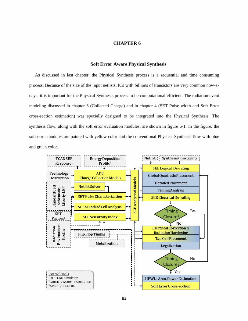
83
CHAPTER 6
6. Soft Error Aware Physical Synthesis
As discussed in last chapter, the Physical Synthesis process is a sequential and time consuming
process. Because of the size of the input netlists, ICs with billions of transistors are very common now-a-
days, it is important for the Physical Synthesis process to be computational efficient. The radiation event
modeling discussed in chapter 3 (Collected Charge) and in chapter 4 (SET Pulse width and Soft Error
cross-section estimation) was specially designed to be integrated into the Physical Synthesis. The
synthesis flow, along with the soft error evaluation modules, are shown in figure 6-1. In the figure, the
soft error modules are painted with yellow color and the conventional Physical Synthesis flow with blue
and green color.
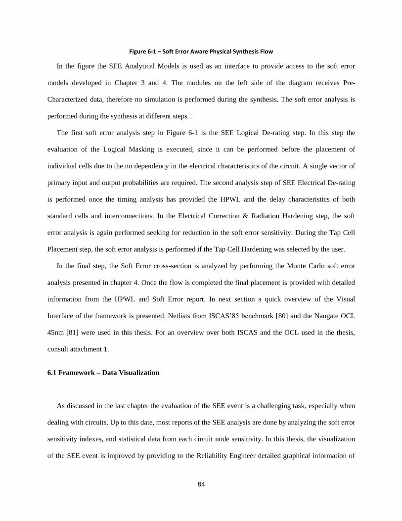
84
Figure 6-1 – Soft Error Aware Physical Synthesis Flow
In the figure the SEE Analytical Models is used as an interface to provide access to the soft error
models developed in Chapter 3 and 4. The modules on the left side of the diagram receives Pre-
Characterized data, therefore no simulation is performed during the synthesis. The soft error analysis is
performed during the synthesis at different steps. .
The first soft error analysis step in Figure 6-1 is the SEE Logical De-rating step. In this step the
evaluation of the Logical Masking is executed, since it can be performed before the placement of
individual cells due to the no dependency in the electrical characteristics of the circuit. A single vector of
primary input and output probabilities are required. The second analysis step of SEE Electrical De-rating
is performed once the timing analysis has provided the HPWL and the delay characteristics of both
standard cells and interconnections. In the Electrical Correction & Radiation Hardening step, the soft
error analysis is again performed seeking for reduction in the soft error sensitivity. During the Tap Cell
Placement step, the soft error analysis is performed if the Tap Cell Hardening was selected by the user.
In the final step, the Soft Error cross-section is analyzed by performing the Monte Carlo soft error
analysis presented in chapter 4. Once the flow is completed the final placement is provided with detailed
information from the HPWL and Soft Error report. In next section a quick overview of the Visual
Interface of the framework is presented. Netlists from ISCAS’85 benchmark [80] and the Nangate OCL
45nm [81] were used in this thesis. For an overview over both ISCAS and the OCL used in the thesis,
consult attachment 1.
6.1 Framework – Data Visualization
As discussed in the last chapter the evaluation of the SEE event is a challenging task, especially when
dealing with circuits. Up to this date, most reports of the SEE analysis are done by analyzing the soft error
sensitivity indexes, and statistical data from each circuit node sensitivity. In this thesis, the visualization
of the SEE event is improved by providing to the Reliability Engineer detailed graphical information of
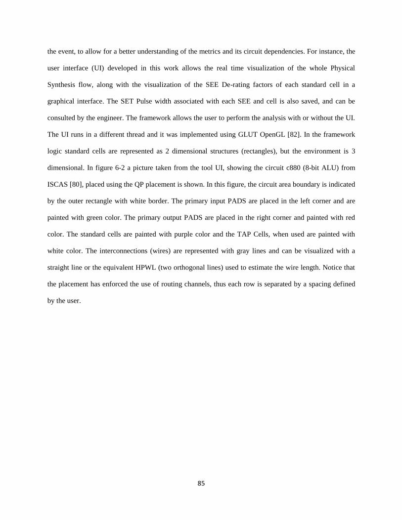
85
the event, to allow for a better understanding of the metrics and its circuit dependencies. For instance, the
user interface (UI) developed in this work allows the real time visualization of the whole Physical
Synthesis flow, along with the visualization of the SEE De-rating factors of each standard cell in a
graphical interface. The SET Pulse width associated with each SEE and cell is also saved, and can be
consulted by the engineer. The framework allows the user to perform the analysis with or without the UI.
The UI runs in a different thread and it was implemented using GLUT OpenGL [82]. In the framework
logic standard cells are represented as 2 dimensional structures (rectangles), but the environment is 3
dimensional. In figure 6-2 a picture taken from the tool UI, showing the circuit c880 (8-bit ALU) from
ISCAS [80], placed using the QP placement is shown. In this figure, the circuit area boundary is indicated
by the outer rectangle with white border. The primary input PADS are placed in the left corner and are
painted with green color. The primary output PADS are placed in the right corner and painted with red
color. The standard cells are painted with purple color and the TAP Cells, when used are painted with
white color. The interconnections (wires) are represented with gray lines and can be visualized with a
straight line or the equivalent HPWL (two orthogonal lines) used to estimate the wire length. Notice that
the placement has enforced the use of routing channels, thus each row is separated by a spacing defined
by the user.
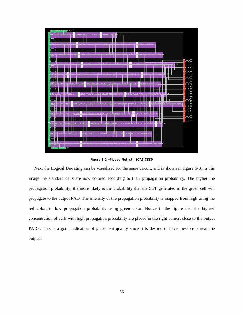
86
Figure 6-2 –Placed Netlist- ISCAS C880
Next the Logical De-rating can be visualized for the same circuit, and is shown in figure 6-3. In this
image the standard cells are now colored according to their propagation probability. The higher the
propagation probability, the more likely is the probability that the SET generated in the given cell will
propagate to the output PAD. The intensity of the propagation probability is mapped from high using the
red color, to low propagation probability using green color. Notice in the figure that the highest
concentration of cells with high propagation probability are placed in the right corner, close to the output
PADS. This is a good indication of placement quality since it is desired to have these cells near the
outputs.
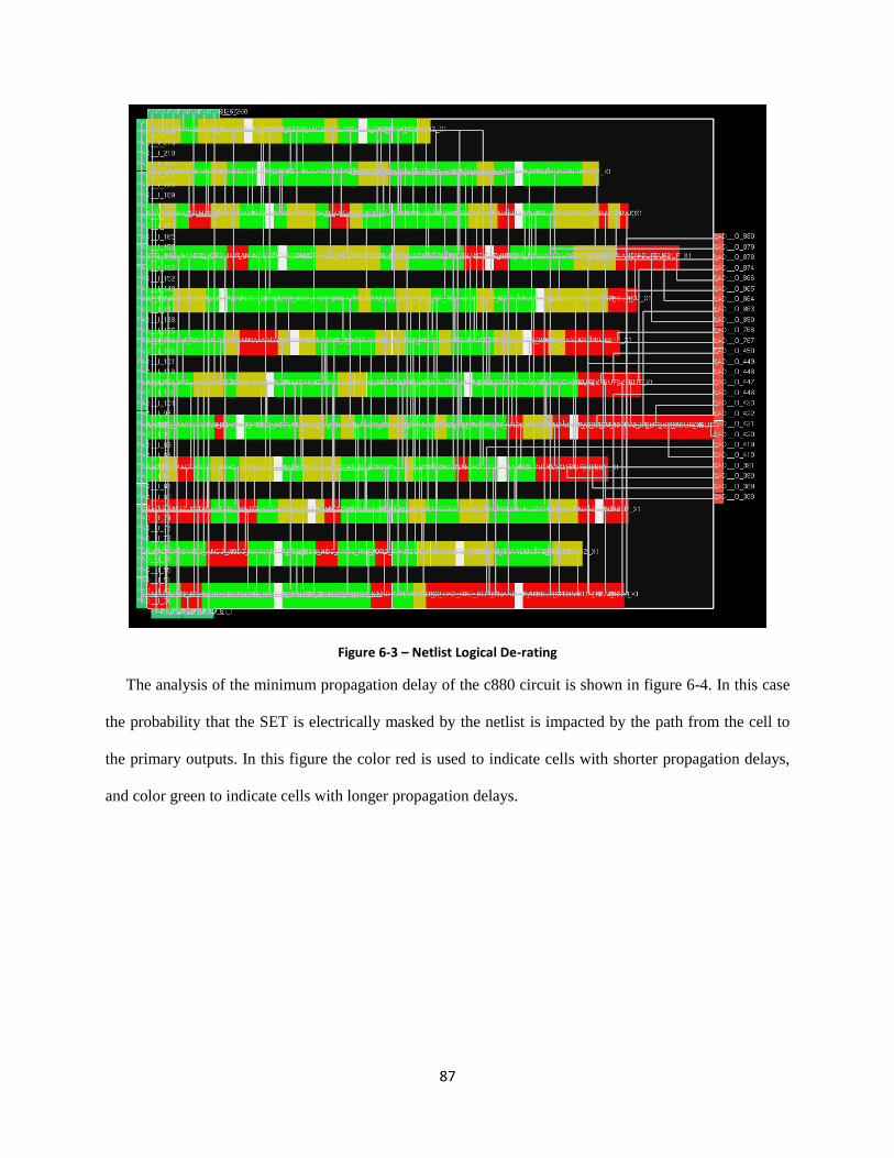
87
Figure 6-3 – Netlist Logical De-rating
The analysis of the minimum propagation delay of the c880 circuit is shown in figure 6-4. In this case
the probability that the SET is electrically masked by the netlist is impacted by the path from the cell to
the primary outputs. In this figure the color red is used to indicate cells with shorter propagation delays,
and color green to indicate cells with longer propagation delays.
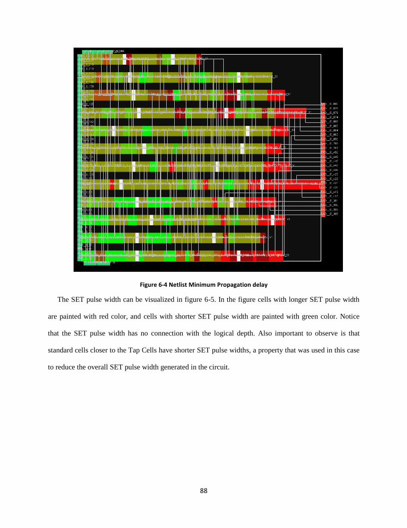
88
Figure 6-4 Netlist Minimum Propagation delay
The SET pulse width can be visualized in figure 6-5. In the figure cells with longer SET pulse width
are painted with red color, and cells with shorter SET pulse width are painted with green color. Notice
that the SET pulse width has no connection with the logical depth. Also important to observe is that
standard cells closer to the Tap Cells have shorter SET pulse widths, a property that was used in this case
to reduce the overall SET pulse width generated in the circuit.
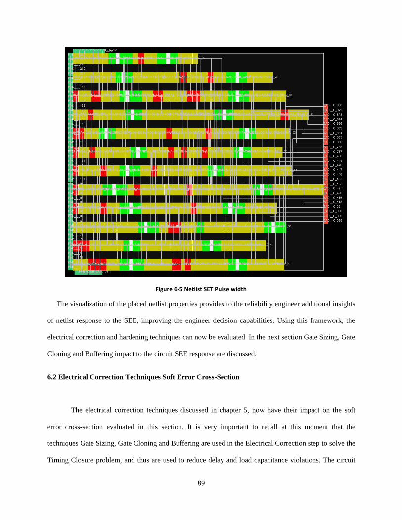
89
Figure 6-5 Netlist SET Pulse width
The visualization of the placed netlist properties provides to the reliability engineer additional insights
of netlist response to the SEE, improving the engineer decision capabilities. Using this framework, the
electrical correction and hardening techniques can now be evaluated. In the next section Gate Sizing, Gate
Cloning and Buffering impact to the circuit SEE response are discussed.
6.2 Electrical Correction Techniques Soft Error Cross-Section
The electrical correction techniques discussed in chapter 5, now have their impact on the soft
error cross-section evaluated in this section. It is very important to recall at this moment that the
techniques Gate Sizing, Gate Cloning and Buffering are used in the Electrical Correction step to solve the
Timing Closure problem, and thus are used to reduce delay and load capacitance violations. The circuit
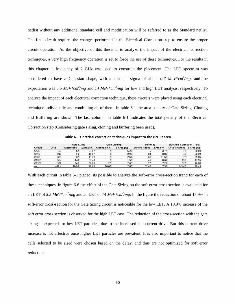
90
netlist without any additional standard cell and modification will be referred to as the Standard netlist.
The final circuit requires the changes performed in the Electrical Correction step to ensure the proper
circuit operation. As the objective of this thesis is to analyze the impact of the electrical correction
techniques, a very high frequency operation is set to force the use of these techniques. For the results in
this chapter, a frequency of 2 GHz was used to constrain the placement. The LET spectrum was
considered to have a Gaussian shape, with a constant sigma of about 0.7 MeV*cm2/mg, and the
expectation was 5.5 MeV*cm2/mg and 14 MeV*cm
2/mg for low and high LET analysis, respectively. To
analyze the impact of each electrical correction technique, these circuits were placed using each electrical
technique individually and combining all of them. In table 6-1 the area penalty of Gate Sizing, Cloning
and Buffering are shown. The last column on table 6-1 indicates the total penalty of the Electrical
Correction step (Considering gate sizing, cloning and buffering been used).
Table 6-1 Electrical correction techniques impact to the circuit area
With each circuit in table 6-1 placed, its possible to analyze the soft-error cross-section trend for each of
these techniques. In figure 6-6 the effect of the Gate Sizing on the soft-error cross section is evaluated for
an LET of 5.5 MeV*cm2/mg and an LET of 14 MeV*cm
2/mg. In the figure the reduction of about 15.9% in
soft-error cross-section for the Gate Sizing circuit is noticeable for the low LET. A 13.9% increase of the
soft error cross section is observed for the high LET case. The reduction of the cross-section with the gate
sizing is expected for low LET particles, due to the increased cell current drive. But this current drive
increase is not effective once higher LET particles are prevalent. It is also important to notice that the
cells selected to be sized were chosen based on the delay, and thus are not optimized for soft error
reduction.
Circuit Cells Sized cells Δ Area (%) Cloned cells Δ Area (%) Buffers Added Δ Area (%) Cells Changed Δ Area (%)
C432 168 62 51.67 7 5.20 5 3.72 72 60.59
C499 210 16 10.67 8 2.93 24 8.80 48 22.39
C880 383 32 11.70 8 2.57 36 11.58 72 25.85
C1355 554 148 37.40 8 1.53 45 8.61 196 47.55
C1908 932 245 36.80 22 2.06 77 7.21 329 46.08
Avg 449.4 100.6 29.65 10.60 2.86 37.40 7.98 143.40 40.49
Gate Sizing Gate Cloning Buffering Electrical Correction - Total
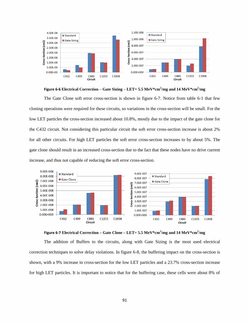
91
Figure 6-6 Electrical Correction – Gate Sizing – LET= 5.5 MeV*cm2/mg and 14 MeV*cm
2/mg
The Gate Clone soft error cross-section is shown in figure 6-7. Notice from table 6-1 that few
cloning operations were required for these circuits, so variations in the cross-section will be small. For the
low LET particles the cross-section increased about 10.8%, mostly due to the impact of the gate clone for
the C432 circuit. Not considering this particular circuit the soft error cross-section increase is about 2%
for all other circuits. For high LET particles the soft error cross-section increases to by about 5%. The
gate clone should result in an increased cross-section due to the fact that these nodes have no drive current
increase, and thus not capable of reducing the soft error cross-section.
Figure 6-7 Electrical Correction – Gate Clone – LET= 5.5 MeV*cm2/mg and 14 MeV*cm
2/mg
The addition of Buffers to the circuits, along with Gate Sizing is the most used electrical
correction techniques to solve delay violations. In figure 6-8, the buffering impact on the cross-section is
shown, with a 9% increase in cross-section for the low LET particles and a 23.7% cross-section increase
for high LET particles. It is important to notice that for the buffering case, these cells were about 8% of

92
the circuit, and have a direct impact on the cross-section, with about 9% cross-section increase for low
LET particles.
Figure 6-8 Electrical Correction – Buffering – LET= 5.5 MeV*cm2/mg and 14 MeV*cm
2/mg
Now the techniques discussed before are combined, as they would be in a synthesis step. In figure
6-9 the soft error cross-section is shown for both low and high LET case. For the low LET case the soft-
error cross section increases about 15%. For the high LET case the increase of the soft-error cross-section
is consistent for all circuits, with an average increase of 45%.
Figure 6-9 Electrical Correction – LET= 5.5 MeV*cm2/mg and 14 MeV*cm
2/mg
Electrical correction techniques do have a direct impact to the circuit soft-error cross-section and
should be properly evaluated in the design flow. The use of buffers and gate clone will increase the soft-
error cross-section if the additional cells are vulnerable to the given LET particle, therefore these
operations should be used carefully if the soft error rate is a concern. The specification of the radiation
environment (fluence and energy spectrum) are very important to determinate the expected circuit soft-
error cross-section. The circuit soft error response will strongly depend on the radiation environment
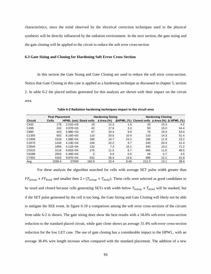
93
characteristics, since the trend observed by the electrical correction techniques used in the physical
synthesis will be directly influenced by the radiation environment. In the next section, the gate sizing and
the gate cloning will be applied to the circuit to reduce the soft error cross-section
6.3 Gate Sizing and Cloning for Hardening Soft Error Cross-Section
In this section the Gate Sizing and Gate Cloning are used to reduce the soft error cross-section.
Notice that Gate Cloning in this case is applied as a hardening technique as discussed in chapter 5, section
2. In table 6-2 the placed netlists generated for this analysis are shown with their impact on the circuit
area.
Table 6-2 Radiation hardening techniques impact to the circuit area
For these analysis the algorithm searched for cells with average SET pulse width greater than
𝐹𝐹𝑆𝑒𝑡𝑢𝑝 + 𝐹𝐹𝐻𝑜𝑙𝑑 and smaller then 2 ∗ (𝑇𝑆𝑒𝑡𝑢𝑝 + 𝑇𝐻𝑜𝑙𝑑). These cells were selected as good candidates to
be sized and cloned because cells generating SETs with width below 𝑇𝑆𝑒𝑡𝑢𝑝 + 𝑇𝐻𝑜𝑙𝑑 will be masked, but
if the SET pulse generated by the cell is too long, the Gate Sizing and Gate Cloning will likely not be able
to mitigate the SEE event. In figure 6-10 a comparison among the soft error cross-sections of the circuits
from table 6-2 is shown. The gate sizing does show the best results with a 58.6% soft-error cross-section
reduction to the standard placed circuit, while gate clone shows an average 31.4% soft-error cross-section
reduction for the low LET case. The use of gate cloning has a considerable impact to the HPWL, with an
average 38.4% wire length increase when compared with the standard placement. The addition of a new
Circuit Cells HPWL (um) Sized cells Δ Area (%) ΔHPWL (%) Cloned cells Δ Area (%) Δ HPWL (%)
C432 178 2.51E+03 19 12.3 1.0 33 15.3 4.2
C499 242 3.97E+03 42 17.6 3.3 50 15.0 44.4
C880 423 5.88E+03 57 20.4 9.9 76 19.4 53.0
C1355 602 8.16E+03 110 20.0 10.4 110 14.3 51.4
C1908 1016 1.58E+04 186 16.7 23.2 186 11.9 23.2
C2670 1434 4.13E+04 156 22.2 9.7 240 20.4 41.4
C3540 1859 4.11E+04 132 7.3 15.1 340 10.2 71.2
C5315 3116 9.81E+04 276 11.5 6.7 466 11.6 48.5
C6288 2552 5.46E+04 0 0.0 0.0 26 0.7 4.5
C7552 4162 9.87E+04 631 26.4 14.6 596 12.1 41.9
Avg 1558.4 37009 160.9 15.4 9.40 212.3 13.1 38.4
Post Placement Hardening Sizing Hardening Cloning
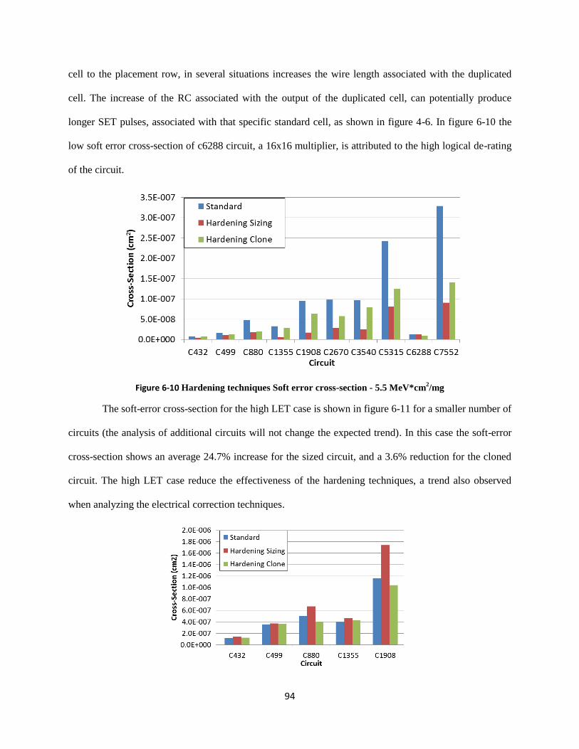
94
cell to the placement row, in several situations increases the wire length associated with the duplicated
cell. The increase of the RC associated with the output of the duplicated cell, can potentially produce
longer SET pulses, associated with that specific standard cell, as shown in figure 4-6. In figure 6-10 the
low soft error cross-section of c6288 circuit, a 16x16 multiplier, is attributed to the high logical de-rating
of the circuit.
Figure 6-10 Hardening techniques Soft error cross-section - 5.5 MeV*cm2/mg
The soft-error cross-section for the high LET case is shown in figure 6-11 for a smaller number of
circuits (the analysis of additional circuits will not change the expected trend). In this case the soft-error
cross-section shows an average 24.7% increase for the sized circuit, and a 3.6% reduction for the cloned
circuit. The high LET case reduce the effectiveness of the hardening techniques, a trend also observed
when analyzing the electrical correction techniques.
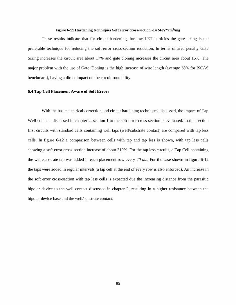
95
Figure 6-11 Hardening techniques Soft error cross-section -14 MeV*cm2/mg
These results indicate that for circuit hardening, for low LET particles the gate sizing is the
preferable technique for reducing the soft-error cross-section reduction. In terms of area penalty Gate
Sizing increases the circuit area about 17% and gate cloning increases the circuit area about 15%. The
major problem with the use of Gate Cloning is the high increase of wire length (average 38% for ISCAS
benchmark), having a direct impact on the circuit routability.
6.4 Tap Cell Placement Aware of Soft Errors
With the basic electrical correction and circuit hardening techniques discussed, the impact of Tap
Well contacts discussed in chapter 2, section 1 to the soft error cross-section is evaluated. In this section
first circuits with standard cells containing well taps (well\substrate contact) are compared with tap less
cells. In figure 6-12 a comparison between cells with tap and tap less is shown, with tap less cells
showing a soft error cross-section increase of about 210%. For the tap less circuits, a Tap Cell containing
the well\substrate tap was added in each placement row every 40 um. For the case shown in figure 6-12
the taps were added in regular intervals (a tap cell at the end of every row is also enforced). An increase in
the soft error cross-section with tap less cells is expected due the increasing distance from the parasitic
bipolar device to the well contact discussed in chapter 2, resulting in a higher resistance between the
bipolar device base and the well/substrate contact.
96
Figure 6-12 Soft-error cross-section comparison between cells with tap and tap less cells – 5.5 MeV*cm2/mg.
With the increase in soft-error cross-section resulting from the use of tap less standard cells, a
placement algorithm is proposed in this thesis to reduce the impact of tap less cells to the soft error cross-
section. Considering that the Standard Tap Cell algorithm places cells at regular intervals according to
DRC rules, it is proposed in this thesis to optimize the tap cell position according the SET pulse width of
the cells in the given placement row. In this work, the Tap Cell position is given by both a minimum
required distance from the standard cells to the Tap Cell (as done in the standard tap placement algorithm)
and the tap cell position that minimizes the SET pulse width in a given placement row section.
The algorithm, now referred to as the Tap Hardening algorithm simply divide the placement row
into segments according to the minimum required distance from the standard cell to the tap cell (in this
case 40um). Now within this segment the algorithm iterates over each cell position and calculate the total
SET pulse width of all cells in the row segment. The final tap cell position will be the one with minimum
total SET pulse width. For this analysis to ensure a fair comparison between the standard tap placement
and the hardening tap placement, the number of Tap Cells used for each technique was constant, therefore
in each placement row the number of tap cells used by the hardening technique and the standard tap
placement are the same. In table 6-3 the impact of the tap cell placement techniques to the HPWL is
shown, with the Tap Hardening technique causing a very small increase to the HPWL.
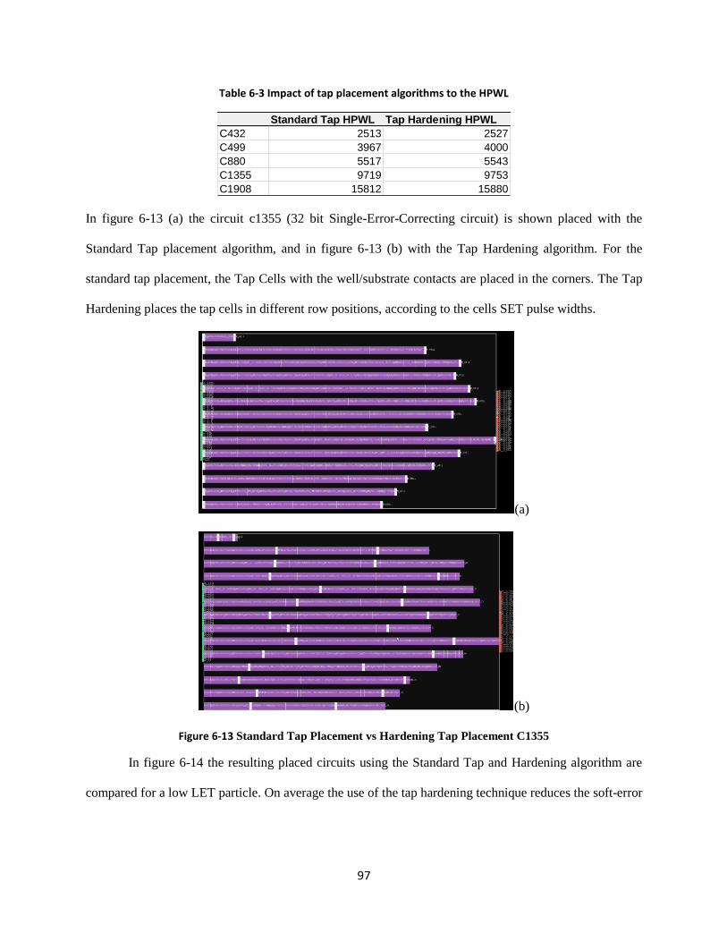
97
Table 6-3 Impact of tap placement algorithms to the HPWL
In figure 6-13 (a) the circuit c1355 (32 bit Single-Error-Correcting circuit) is shown placed with the
Standard Tap placement algorithm, and in figure 6-13 (b) with the Tap Hardening algorithm. For the
standard tap placement, the Tap Cells with the well/substrate contacts are placed in the corners. The Tap
Hardening places the tap cells in different row positions, according to the cells SET pulse widths.
(a)
(b)
Figure 6-13 Standard Tap Placement vs Hardening Tap Placement C1355
In figure 6-14 the resulting placed circuits using the Standard Tap and Hardening algorithm are
compared for a low LET particle. On average the use of the tap hardening technique reduces the soft-error
Standard Tap HPWL Tap Hardening HPWL
C432 2513 2527
C499 3967 4000
C880 5517 5543
C1355 9719 9753
C1908 15812 15880
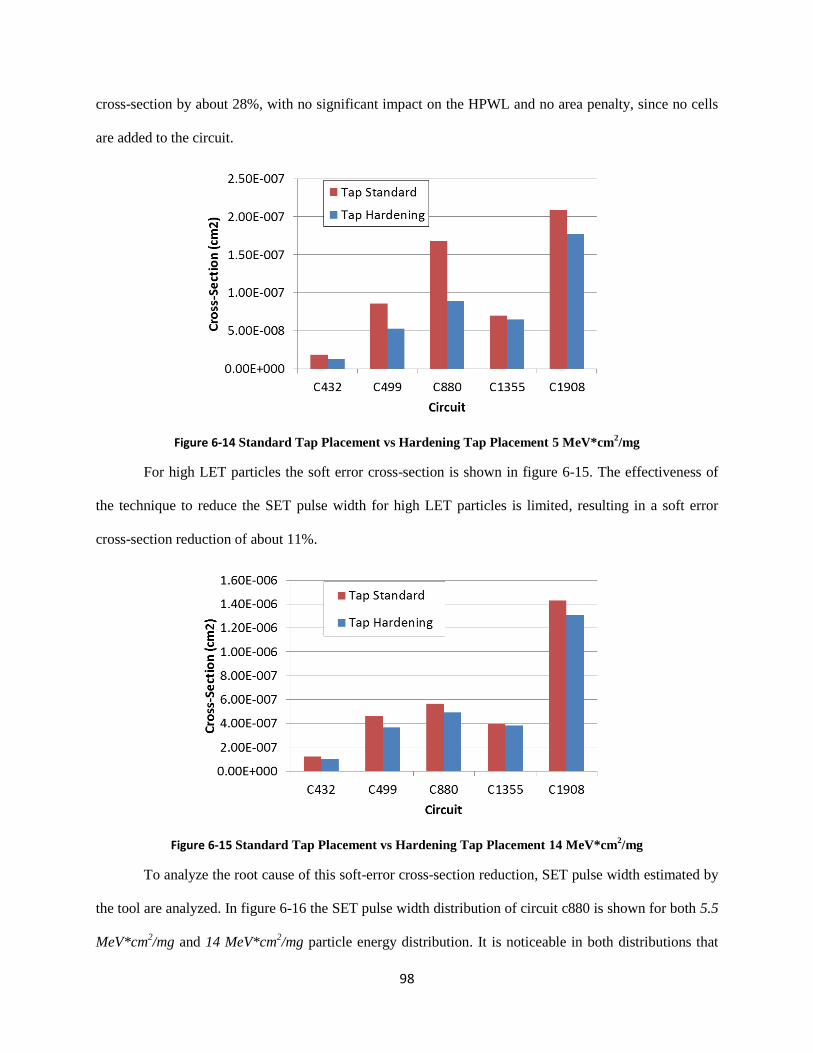
98
cross-section by about 28%, with no significant impact on the HPWL and no area penalty, since no cells
are added to the circuit.
Figure 6-14 Standard Tap Placement vs Hardening Tap Placement 5 MeV*cm2/mg
For high LET particles the soft error cross-section is shown in figure 6-15. The effectiveness of
the technique to reduce the SET pulse width for high LET particles is limited, resulting in a soft error
cross-section reduction of about 11%.
Figure 6-15 Standard Tap Placement vs Hardening Tap Placement 14 MeV*cm2/mg
To analyze the root cause of this soft-error cross-section reduction, SET pulse width estimated by
the tool are analyzed. In figure 6-16 the SET pulse width distribution of circuit c880 is shown for both 5.5
MeV*cm2/mg and 14 MeV*cm
2/mg particle energy distribution. It is noticeable in both distributions that
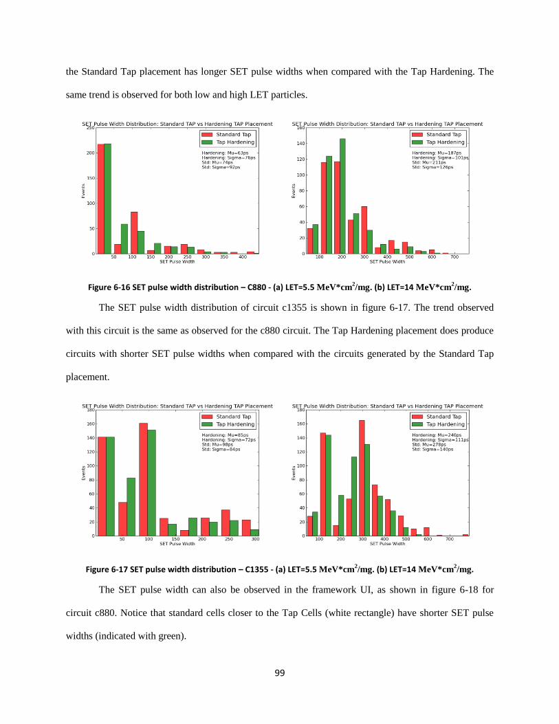
99
the Standard Tap placement has longer SET pulse widths when compared with the Tap Hardening. The
same trend is observed for both low and high LET particles.
Figure 6-16 SET pulse width distribution – C880 - (a) LET=5.5 MeV*cm2/mg. (b) LET=14 MeV*cm
2/mg.
The SET pulse width distribution of circuit c1355 is shown in figure 6-17. The trend observed
with this circuit is the same as observed for the c880 circuit. The Tap Hardening placement does produce
circuits with shorter SET pulse widths when compared with the circuits generated by the Standard Tap
placement.
Figure 6-17 SET pulse width distribution – C1355 - (a) LET=5.5 MeV*cm2/mg. (b) LET=14 MeV*cm
2/mg.
The SET pulse width can also be observed in the framework UI, as shown in figure 6-18 for
circuit c880. Notice that standard cells closer to the Tap Cells (white rectangle) have shorter SET pulse
widths (indicated with green).
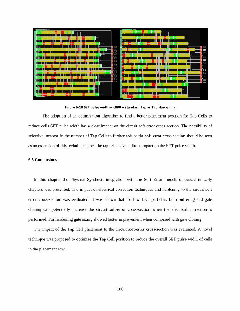
100
Figure 6-18 SET pulse width – c880 – Standard Tap vs Tap Hardening
The adoption of an optimization algorithm to find a better placement position for Tap Cells to
reduce cells SET pulse width has a clear impact on the circuit soft-error cross-section. The possibility of
selective increase in the number of Tap Cells to further reduce the soft-error cross-section should be seen
as an extension of this technique, since the tap cells have a direct impact on the SET pulse width.
6.5 Conclusions
In this chapter the Physical Synthesis integration with the Soft Error models discussed in early
chapters was presented. The impact of electrical correction techniques and hardening to the circuit soft
error cross-section was evaluated. It was shown that for low LET particles, both buffering and gate
cloning can potentially increase the circuit soft-error cross-section when the electrical correction is
performed. For hardening gate sizing showed better improvement when compared with gate cloning.
The impact of the Tap Cell placement to the circuit soft-error cross-section was evaluated. A novel
technique was proposed to optimize the Tap Cell position to reduce the overall SET pulse width of cells
in the placement row.
101
CHAPTER 7
Conclusions
In this work a computationally feasible approach to model the Soft Error event in the Physical
Synthesis process is presented. By using a combination of analytical models and lookup tables soft error
event were modeled for different technologies, using a flexible and robust framework.
This thesis first, expands the ADC model used to estimate collected charge for the multiple transistor
charge collection case. By using the ADC, detailed characteristics of the SEE event can be dynamically
computed by the framework, without much computational impact. Results were validated with TCAD
data, showing good model accuracy.
A methodology to estimate the SET pulse width was developed to model the SEE response of multiple
standard cells, with limited pre-characterization. By using only 3 lookup tables and the standard cell
circuit analysis, the SET pulse width can be accurately estimated. Results were validated using SPICE
simulations and experimental SET pulse width data from a 45nm Test Chip. To measure the circuit SEE
response, a Monte Carlo analysis using probability matrices was developed. The model is able to estimate
the circuit soft-error cross-section with a good accuracy and it was validated using data from a 45nm Test
Chip.
With the Soft Error analysis methodology implemented, the Physical Synthesis flow was modeled.
Two placement algorithms based on Monte Carlo Simulated Annealing and Quadratic Programming were
implemented and evaluated in this work. The Physical synthesis flow was partially implemented covering
the Timing Analysis, Electrical Correction, Detailed Placement and Legalization algorithms.
The electrical correction techniques, Gate Sizing, Gate Cloning and Buffering had their impact to the
circuit soft error cross-section evaluated. It was found out that the electrical correction is going to increase
the circuit soft-error cross-section if the cells added to the circuit are vulnerable to the analyzed radiation
102
environment. The use of buffers are particular likely to increase the soft-error cross-section if the particle
is able to upset these cells. The Gate Sizing and Gate Cloning as circuit hardening techniques were also
evaluated. Results have shown a better efficiency of Gate Sizing to reduce the circuit soft error cross-
section when compared to the gate cloning. The high wire length increase occasioned due to the Gate
Cloning is another drawback to the use of this technique for hardening circuits against soft errors.
The use of the circuit hardening techniques like Gate Sizing and Gate Cloning should be used with
care, due to the limitation of these techniques to mitigate low LET particles. The radiation environment
should be carefully evaluated, before consider the use of these circuit operations as hardening techniques.
As demonstrated in this thesis, the methodology proposed is able to detect these trends and provide
valuable information about the circuit soft error response.
An algorithm to reduce the circuit soft error cross-section by optimizing the Tap Cell placement was
proposed. The algorithm was able to generate circuits with consistent reduced soft-error cross-section
when compared with circuits generated by standard tap cell placement algorithms. The better placement
of the Tap Cells has a consistent impact on the soft-error cross-section for both low and high LET
particles.
A design flow to allow the integration of the soft error analysis into the Physical Synthesis without
disrupting the standard ASIC design flow used by the industry was developed. By adopting two metrics to
evaluate the soft error event (soft error sensitivity index and the cross section calculation) in different
steps of the design flow, the soft error evaluation can be effectively integrated into the Physical Synthesis.
Lastly, the capabilities of the resulting framework developed in this thesis to analyze circuits and
provide detailed information from the soft error event was shown. The framework enables the traceability
of the SEE events to identify the root-cause of events and circuit characteristics impacting the standard
cell response.
Future work includes the modeling of collected charge and charge sharing on FinFET transistors and
the evaluation of this analysis to estimate the soft-error cross-section of sequential circuits.
103
REFERENCES
[1] R. Baumann, "Radiation-Induced Soft Error in Advanced Semiconductor Technologies," IEEE Trans.
Devi. Mate. Reli., vol. 5, no. 3, pp. 305-316, Sept. 2005.
[2] L. Massengill, B. Bhuva, W. Holman, M. Alles and T. Loveless, "Technology scaling and soft error
reliability," in IEEE International Reliability Physics Symposium (IRPS), Anaheim, 2012.
[3] R. Reed, R. Weller, M. Mendenhall, J.-M. Lauenstein, K. Warren, J. Pellish, R. Schrimpf, B. Sierawski,
L. Massengill, P. Dodd, M. Shaneyfelt, J. Felix, J. Schwank, N. Haddad, R. Lawrence and J. Bowman,
"Impact of Ion Energy and Species on Single Event Effects Analysis," IEEE Trans. Nucl. Sci., vol. 54,
no. 6, pp. 2312 - 2321, Dec. 2007.
[4] N. Atkinson, J. Ahlbin, A. Witulski, N. Gaspard, W. Holman, B. Bhuva, E. Zhang, L. Chen and L.
Massengill, "Effect of Transistor Density and Charge Sharing on Single-Event Transients in 90-nm
Bulk CMOS," IEEE Trans. Nucl. Sci., vol. 58, no. 6, pp. 2578 - 2584, Oct. 2011.
[5] R. Brayton and J. Cong, "Electronic Design Automation Past, Present, Future," NSF Workshop
Report, Arlington, VA, 2009.
[6] NVIDIA Corporation, "NVIDIA’s Next Generation - Kepler TM GK110," 1 1 2012. [Online]. Available:
http://www.nvidia.com/content/PDF/kepler/NVIDIA-Kepler-GK110-Architecture-Whitepaper.pdf.
[Accessed 1 11 2014].
[7] C. Alpert, C. Chu and P. Villarrubia, "The Coming of Age of Physical Synthesi," in IEEE/ACM
International Conference on Computer-Aided Design (ICCAD), San Jose, CA, 2007.
[8] K. Bhattacharya and N. Ranganathan, "A New Placement Algorithm for Reduction of Soft Errors in
Macrocell Based Design of Nanometer Circuits.," in VLSI, IEEE Computer Society Annual Symposium
on, Tampa, 2009.
[9] K. Bhattacharya and N. Ranganathan, "Placement for Immunity of Transient Faults in Cell-Based
Design of Nanometer Circuits," IEEE Transactions on Very Large Scale Integration (VLSI) Systems,
vol. 19, no. 5, pp. 918 - 923, Apri. 2011.
[10] L. Entrena, A. Lindoso, E. Millan, S. Pagliarini, F. Almeida and F. Kastensmidt, "Constrained
Placement Methodology for Reducing SER Under Single-Event-Induced Charge Sharing Effects," IEEE
Trans. Nucl. Sci., vol. 59, no. 4, pp. 811 - 817, Apr. 2012.
104
[11] D. Yankang and B. L. S. Chen, "A Constrained Layout Placement Approach to Enhance Pulse
Quenching Effect in Large Combinational Circuits," IEEE Trans. Devi. Mate. Reli., vol. 14, no. 1, pp.
268 - 274, Nov. 2013.
[12] J. R. Ahlbin, L. W. Massengill, B. L. Bhuva, B. Narasimham, M. J. Gadlage and P. H. Eaton, "Single-
Event Transient Pulse Quenching in Advanced CMOS Logic Circuits," IEEE Trans. Nucl. Sci., vol. 56,
no. 6, pp. 3050-3056, Dec. 2009.
[13] N. Rezzak, TOTAL IONIZING DOSE EFFECTS IN ADVANCED CMOS TECHNOLOGIES, Nashville:
Vanderbilt Thesis, 2012.
[14] S. Jagannathan, Portable Behavioral Modeling of TID Degradation of Voltage Feedback Op-Amps,
Nashville: Vanderbilt Thesis, 2009.
[15] C. Hu, "Alfa-Particle-Indeuced Field and Enhanced Collection," IEEE Elec. Dev. Letters, vol. 3, no. 2,
pp. 31-34, 1982.
[16] W. G. Bennett, EFFICIENT CHARACTERIZATION OF TRANSIENT PULSE SHAPES FROM RADIATION
INDUCED UPSETS, Nashville T: Vanderbilt - PhD Thesis, 2012.
[17] O. A. Amusan, Effects of Single-Event-Induced Charge Sharing in sub-100nm bulk CMOS
technologies, Nashville, TN: Vanderbilt - PhD Thesis, 2009.
[18] I. Chatterjee, SINGLE-EVENT CHARGE COLLECTION AND UPSET IN 65-NM AND 40-NM DUAL- AND
TRIPLE-WELL BULK CMOS SRAMS, Nashville: Vanderbilt - Thesis, 2012.
[19] N. J. Gaspard, IMPACT OF WELL STRUCTURE ON SE RESPONSE IN 90-nm BULK CMOS, Nashville:
Vanderbilt - Thesis, 2011.
[20] O. Amusan, A. Witulski, L. Massengill, B. Bhuva, P. Fleming, M. Alles, A. Sternberg, J. Black and R.
Schrimpf, "Charge Collection and Charge Sharing in a 130 nm CMOS Technology," IEEE Transactions
on Nuclear Science, vol. 53, no. 6, pp. 3253-3258, 2006.
[21] O. Amusan, L. Massengill, M. Baze, B. Bhuva, A. Witulski, J. Black, A. Balasubramanian, M. Casey, D.
Black, J. Ahlbin, R. Reed and M. McCurdy, "Mitigation techniques for single event induced charge
sharing in a 90 nm bulk CMOS process," IEEE International Reliability Physics Symposium, pp. 468-
472, 27 April 2008.
[22] J. F. Ziegler, J. P. Biersack and M. D. Ziegler, The Stopping and Range of Ions in Matter, Pergamon
Press, 1977-1985.
[23] J. Allison, K. Amako, J. Apostolakis, H. Araujo, P. Dubois, M. Asai, G. Barrand, R. Capra, S. Chauvie, R.
Chytracek, G. Cirrone, G. Cooperman, G. Cosmo and e. al., "Geant4 developments and
105
applications," IEEE Trans. Nucl. Sci., vol. 53, no. 1, pp. 270-278, Feb. 2006.
[24] R. F. Pierret, Semiconductor Device Fundamentals, -: Addison-Wesley, 1996.
[25] K. Warren, A. Sternberg, R. Weller, M. Baze, L. Massengill, R. Reed, M. Mendenhall and R. Schrimpf,
"Integrating Circuit Level Simulation and Monte-Carlo Radiation Transport Code for Single Event
Upset Analysis in SEU Hardened Circuitry," IEEE Trans. Nucl. Sci. , vol. 55, no. 6, pp. 2886-2894, Dec.
2008.
[26] J. Kauppila, T. Haeffner, D. Ball, A. Kauppila, T. Loveless, S. Jagannathan, A. Sternberg, B. Bhuva and
L. Massengill, "Circuit-Level Layout-Aware Single-Event Sensitive-Area Analysis of 40-nm Bulk CMOS
Flip-Flops Using Compact Modeling," IEEE Trans. Nucl. Sci., vol. 58, no. 6, pp. 2680-2686, Nov. 2011.
[27] R. Weller, M. Mendenhall, R. Reed, R. Schrimpf, K. Warren, B. Sierawski and L. Massengill, "Monte
Carlo Simulation of Single Event Effects," IEEE Trans. Nucl. Sci., vol. 57, no. 4, pp. 1726-1746, Aug.
2010.
[28] J. S. Kaupilla, A. L. Sternberg, M. L. Alles, A. M. Francis, J. Holmes, O. A. Amusan and L. Massengill,
"A Bias-Dependent Single-Event Compact Model Implemented Into BSIM4 and a 90 nm CMOS
Process Design Kit," IEEE Trans. Nucl. Sci., vol. 56, no. 6, pp. 3152-3157, Dec. 2009.
[29] J. N. Bradford, "Geometric Analysis of Soft Errors and Oxide Damage Produced by Heavy Cosmic
Rays and Alpha Particles," IEEE Trans. Nucl. Sci., vol. 27, no. 1, pp. 942-947, Feb. 1980.
[30] E. Petersen, J. Pickel, J. Adams and E. Smith, "Rate Prediction for Single Event Effects – a Critique,"
IEEE Trans. Nucl. Sci., vol. 39, no. 6, pp. 1577-1599, Dec. 1992.
[31] G. Messenger, "Collection of Charge on Junction Nodes from Ion Tracks," IEEE Trans. Nucl. Sci., vol.
29, no. 6, pp. 2024-2031, Dec. 1982.
[32] F. McLean and T. R. Oldham, "Charge Funneling in N- and P-Type Si Substrates," IEEE Trans. Nucl.
Sci., vol. 30, no. 6, pp. 4493-4500, Dec. 1983.
[33] L. Edmonds, "A Theoretical Analysis of the Role of Ambipolar Diffusion in Charge-Carrier Transport
in a Quasi-Neutral Region Under High Injection," IEEE Trans. Nucl. Sci., vol. 58, no. 5, pp. 2459-2469,
Aug. 2011.
[34] N. Hooten, L. Edmonds, W. Bennett, J. Ahlbin, N. Dodds, R. Reed, R. Schrimpf and R. Weller, "The
Significance of High-Level Carrier Generation Conditions for Charge Collection in Irradiated
Devices," IEEE Trans. Nucl. Sci., vol. 59, no. 6, pp. 2710-2721, Dec. 2012.
[35] L. Edmonds, "Extension of the ADC Charge-Collection Model to Include Multiple Junctions," IEEE
Trans. Nucl. Sci., vol. 58, no. 6, pp. 3333-3342, Oct. 2011.
106
[36] Synopsys, Sentaurus TCAD, Mountain View: Synopsys Inc., 2010.
[37] S. DasGupta, TRENDS IN SINGLE EVENT PULSE WIDTHS AND PULSE SHAPES IN DEEP SUBMICRON
CMOS, Nashville: Vanderbilt - Thesis, 2007.
[38] K. Warren, R. Weller, B. Sierawski, R. Reed, M. Mendenhall, R. Schrimpf, L. Massengill, M. Porter, J.
Wilkinson, K. LaBel and J. Adams, "Application of RADSAFE to Model Single Event Upset Response of
a 0.25 um CMOS SRAM," IEEE Trans. Nucl. Sci., vol. 54, no. 4, pp. 898-903, Aug. 2007.
[39] B. Sierawski, R. Reed, R. Schrimpf, K. Warren, R. Weller, M. Mendenhall, J. Black, A. Tipton, M.
Xapsos, R. Baumann, X. Deg, M. Campola, M. Friendlich, H. Kim, A. Phan and C. Seidleck, "Impact of
Low-Energy Proton Induced Upsets on Test Methods and Rate Predictions," IEEE Trans. Nucl. Sci.,
vol. 56, no. 6, pp. 3085-3092, Dec. 2009.
[40] L. Artola, G. Hubert, S. Duzellier and F. Bezerra, "Collected Charge Analysis for a New Transient
Model by TCAD Simulation in 90 nm Technology," IEEE Trans. Nucl. Sci., vol. 57, no. 4, pp. 1869-
1875, Aug. 2010.
[41] L. Artola, G. Hubert, K. Warren, M. Gaillardin, R. Schrimpf, R. Reed, R. Weller, J. Ahlbin and P. e. a.
Paillet, "SEU Prediction From SET Modeling Using Multi-Node Collection in Bulk Transistors and
SRAMs Down to the 65 nm Technology Node," IEEE Trans. Nucl. Sci., vol. 58, no. 3, pp. 1338-1346,
May. 2011.
[42] B. Zhang, W. Wang and M. Orshansky, "FASER: Fast Analysis of Soft Error Susceptibility for Cell-
Based Designs," in IEEE International Symposium on Quality Electronic Design, San Jose, 2006.
[43] R. Rajaraman, N. Vijaykrishnan and Y. Xie, "SEAT-LA: a soft error analysis tool for combinational
logic," IEEE International Conference on Embedded Systems and Design, 3 Jan 2006.
[44] Cadence Design Systems, Virtuoso IC Design, San Jose: Cadence Design Systems Inc, 2010.
[45] ASU, "Predictive Technology Model (PTM)," Arizona State University, 01 01 2012. [Online].
Available: http://ptm.asu.edu/. [Accessed 01 01 2012].
[46] S. Jagannathan, M. Gadlage, B. Bhuva, R. Schrimpf, B. Narasimham, J. Chetia, J. Ahlbin and L.
Massengill, "Independent Measurement of SET Pulse Widths From N-Hits and P-Hits in 65-nm
CMOS," IEEE Trans. Nucl. Sci., vol. 57, no. 6, pp. 3386-3391, Oct. 2010.
[47] L. Massengill, A. Baranski, D. Van Nort, J. Meng and B. Bhuva, "Analysis of single-event effects in
combinational logic-simulation of the AM2901 bitslice processor," IEEE Trans. Nucl. Sci., vol. 47, no.
6, pp. 2609-2615, Dec. 2000.
[48] C. Zhao, S. Dey and X. Bai, "Soft-Spot Analysis: Targeting Compound Noise Effects in Nanometer
107
Circuits," IEEE Trans. Design and Test, vol. 22, no. 4, pp. 362-740, Aug. 2005.
[49] L. W. Massengill, M. S. Reza, B. L. Bhuva and T. L. Turflinger, "Single-event upset cross section
modeling in combinational CMOS logic circuits," Journal Radiation Effects, vol. 16, no. 1, 1998.
[50] N. N. Mahatme, N. J. Gaspard, S. Jagannathan, T. D. Loveless, H. Abdel-Aziz, B. L. Bhuva and L. W.
Massengill, "Estimating the Frequency Threshold for Logic Soft Errors," in IEEE International
Reliability Physics Symposium, Anaheim, 2013.
[51] C. E. Stroud, L.-T. Wang and Y. Chang, "VLSI design flow and typical EDA flow," 1 1 2009. [Online].
Available: http://cc.ee.ntu.edu.tw/~ywchang/Courses/PD/EDA_Chapter1.pdf. [Accessed 03 12
2014].
[52] D. Limbrick, Impact of Logic Synthesis on the Soft Error Rate of Digital Integrated Circuits, Nashville:
Vanderbilt University, 2012.
[53] K. SHAHOOKAR and M. P., "VLSI Cell Placement Techniques," Journal ACM Computing Surveys , vol.
23, no. 2, 1991.
[54] ALTERA Corporation, AN 311: Standard Cell ASIC to FPGA Design Methodology and Guidelines,
Altera, 2009.
[55] L. Hui, I. Markov and e. al., "Keeping Physical Synthesis Safe and Sound," University of Michigan,
Michigan, 2006.
[56] L. N. Kannan, P. R. Suaris and H. G. Fang, "A Methodology and Algorithms for Post-Placement Delay
Optimization," IEEE Design Automation Conference, pp. 327-332, 6-10 Jun. 1994.
[57] Q. Zhou and K. Mohanram, "Gate sizing to radiation harden combinational logic," Computer-Aided
Design of Integrated Circuits and Systems, IEEE Transactions on, vol. 25, no. 1, pp. 155-166, Jan.
2006.
[58] T. Assis, F. Kastensmidt, G. Wirth and R. Reis, "Measuring the effectiveness of symmetric and
asymmetric transistor sizing for Single Event Transient mitigation in CMOS 90nm technologies," in
IEEE Latin-america Test Workshop, Buzios, 2009.
[59] M. Hrkic, J. Lillis and G. Beraudo, "An Approach to Placement-Coupled Logic Replication," IEEE
Design Automation Conference, pp. 711-716, 7-11 Jul. 2004.
[60] T. Heijmen and A. Nieuwland, "Soft-Error Rate Testing of Deep-Submicron Integrated Circuits," in
IEEE European Test Symposium, Southampton, May 2006.
[61] L.P.P.P. Ginneken, "Buffer placement in distributed RC-tree networks for minimal Elmore delay,"
108
IEEE International Symposium on Circuits and Systems, pp. 865-868, 1-3 May 1990.
[62] A. H. Ajami and M. Pedram, "Post-Layout Timing-Driven Cell Placement Using an Accurate Net
Length Model with Movable Steiner Points," IEEE Design Automation Conference, pp. 595-600, 02
Feb. 2001.
[63] I. Markov, J. Hu and M. Kim, "Progress and challenges in VLSI placement research," in IEEE/ACM
International Conference on Computer-Aided Design (ICCAD), San Jose, 2012.
[64] S. KIRKPATRIC, C. GELATT and M. P. VECCHI, "Optimization by Simulated Annealing," Science,, vol.
220, no. 4598, 1983.
[65] Paul E. Black, "Manhattan distance - Dictionary of Algorithms and Data Structures," NIST, 31 May
2006. [Online]. Available: http://www.nist.gov/dads/HTML/manhattanDistance.html. [Accessed 3
12 2014].
[66] C. Sechen and A. Vincentelli, "The TimberWolf Placement and Routing Package," IEEE JOURNAL OF
SOLID-STATE CIRCUITS, vol. 20, no. 2, pp. 510-522, Apri. 1985.
[67] D. Mitra, F. Romeo and A. Sangiovanni-Vincentelli, "Convergence and finite-time behavior of
simulated annealing," in Fort Lauderdale, Fort Lauderdale,, IEEE Conference on Decision and
Control.
[68] J. Kleinhans, G. Sigl, F. Johannes and K. Antreich, "GORDIAN: VLSI placement by quadratic
programming and slicing optimization," IEEE Trans. Computer-Aided Design of Integrated Circuits
and Systems, vol. 10, no. 3, pp. 356 - 365, Aug. 2002.
[69] P. Spindler, U. Schlichtmann and F. Johannes, "Kraftwerk2—A Fast Force-Directed Quadratic
Placement Approach Using an Accurate Net Model," IEEE Transactions on Computer-Aided Design
of Integrated Circuits and Systems, vol. 27, no. 8, pp. 1398 - 1411, May 2008.
[70] L. D. Gaspero., "QuadProg++ project," QuadProg++ , 18 5 2008. [Online]. Available:
http://quadprog.sourceforge.net/. [Accessed 12 12 2014].
[71] A. I. D. Goldfarb, "A numerically stable dual method for solving strictly convex quadratic programs,"
Mathematical Programming, vol. 27, no. 1, pp. pp 1-33, 1983.
[72] S. Goto, "An efficient algorithm for the two-dimensional placement problem in electrical circuit
layout," IEEE Trans. Circ. Syst., vol. 28, no. 1, pp. 12-18, Jan. 2003.
[73] D. Knuth, "Sorting by Merging- Sorting and Searching.," in The Art of Computer Programming 2,
Addison-Wesley, 1998, p. 158–168.
109
[74] M. Pan, N. Viswanathan and C. Chu, "An efficient and effective detailed placement algorithm,"
IEEE/ACM International Conference on Computer-Aided Design, pp. 48 - 55, 6 11 2005.
[75] Synopsys Inc, "Open Source Liberty," Synopsys, Inc., 01 01 2008. [Online]. Available:
https://www.opensourceliberty.org/. [Accessed 01 01 2014].
[76] W. C. Elmore, "The transient response of damped linear networks with particular regard to
wideband amplifiers," Jour. Appl. Phys., vol. 19, no. 1, pp. 55 -63, Jan. 1948.
[77] S. Shi and D. Pan, "Wire sizing with scattering effect for nanoscale interconnection," in Asia and
South Pacific Conference on Design Automation, Yokohama, 2006.
[78] E. Barke, "Line-to-Ground Capacitance Calculation for VLSI: A comparison," IEEE Trans. Computer-
Aided Design, vol. 7, no. 2, pp. 295-298, Feb. 1988.
[79] A. Kahng, J. Lienig, I. Markov and J. Hu, "8 - Timing Closure," in VLSI Physical Design: From Graph
Partitioning to Timing Closure, Springer Netherlands, 2011, pp. 221-262.
[80] ISCAS 85,89, "Benchmark circuits," 02 01 2007. [Online]. Available:
http://www.pld.ttu.ee/~maksim/benchmarks/. [Accessed 13 Aug 2014].
[81] NanGate Inc., "NanGate FreePDK 45nm Open Cell Library," 3 March 2008. [Online]. Available:
http://www.nangate.com/?page_id=2325. [Accessed 8 Jun 2014].
[82] Silicon Graphics International Corp. , "OpenGL," Silicon Graphics International Corp. , 01 01 2008.
[Online]. Available: https://www.opengl.org/resources/libraries/. [Accessed 01 03 2012].
[83] M. Hansen, H.Yalcin and J. Hayes, "Unveiling the ISCAS-85 Benchmarks: A Case Study in Reverse
Engineering," IEEE Design & Test Computers, vol. 16, no. 3, pp. 72-80, 1999.
[84] R. Baumann, "Soft errors in advanced computer systems," in Design & Test of Computers, IEEE,
Dallas, TX., 2005.
[85] W. Kleitz, Digital Electronics: A Practical Approach with VHDL, -: Prentice Hal, 2011.
[86] N. M. Atkinson, SINGLE-EVENT CHARACTERIZATION OF A 90-nm BULK CMOS DIGITAL CELL LIBRARY,
Nashville: Vanderbilt - Master Thesis, 2010.
[87] ITC 99, "ITC 99," 1999. [Online]. Available: http://www.cad.polito.it/downloads/tools/itc99.html.
[Accessed 4 July 2014].
[88] ICCAD, "IEEE CEDA / Taiwan MOE, ICCAD 2014 Contest," 05 11 2014. [Online]. Available:
http://cad_contest.ee.ncu.edu.tw/CAD-Contest-at-ICCAD2014/problem_b/default.html. [Accessed
110
12 Aug 2014].
[89] N.N.Mahatme, Design Techniques for Power-Aware Combinational Logic SER Mitigation, Nashille:
Vanderbilt - PhD Thesis, 2014.
[90] C. Alpert, C. Chu and P. Villarrubia, "The coming of age of physical synthesis," IEEE/ACM
International Conference on Computer-Aided Design, pp. 246-249, 8 Nov 2007.
[91] O. A. Amusan, Analysis of Single Event Vulnerabilities in a 130 nm CMOS Technology, Nashville:
Vanderbilt - Thesis, 2006.
[92] R. A. Reed, R. A. Weller, M. H. Mendenhall, J.-M. Lauenstein, K. M. Warre, J. A. Pellish, R. D.
Schrimpf, B. D. Sierawski and L. W. Massengill, "Impact of Ion Energy and Species on Single Event
Effects Analysis," IEEE Trans. Nucl. Sci., vol. 54, no. 6, pp. 2312-2321, Dec. 2007.
[93] B. Narasimham, B. L. Bhuva, R. D. Schrimpf, L. W. Massengill, M. J. Gadlage and e. al.,
"Characterization of Digital Single Event Transient Pulse-Widths in 130-nm and 90-nm CMOS
Technologies," IEEE Trans. Nucl. Sci., vol. 54, no. 6, pp. 2506-2511, Dec. 2007.
[94] J. D. Black, P. E.Dodd and K. M. Warren, "Physics of Multiple-Node Charge Collection and Impacts
on Single-Event Characterization and Soft Error Rate Prediction," IEEE Trans. Nucl. Sci., vol. 60, no.
3, pp. 1836-1851, May. 2013.
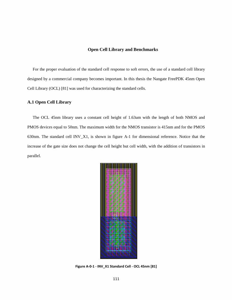
111
Open Cell Library and Benchmarks
For the proper evaluation of the standard cell response to soft errors, the use of a standard cell library
designed by a commercial company becomes important. In this thesis the Nangate FreePDK 45nm Open
Cell Library (OCL) [81] was used for characterizing the standard cells.
A.1 Open Cell Library
The OCL 45nm library uses a constant cell height of 1.63um with the length of both NMOS and
PMOS devices equal to 50nm. The maximum width for the NMOS transistor is 415nm and for the PMOS
630nm. The standard cell INV_X1, is shown in figure A-1 for dimensional reference. Notice that the
increase of the gate size does not change the cell height but cell width, with the addition of transistors in
parallel.
Figure A-0-1 - INV_X1 Standard Cell - OCL 45nm [81]
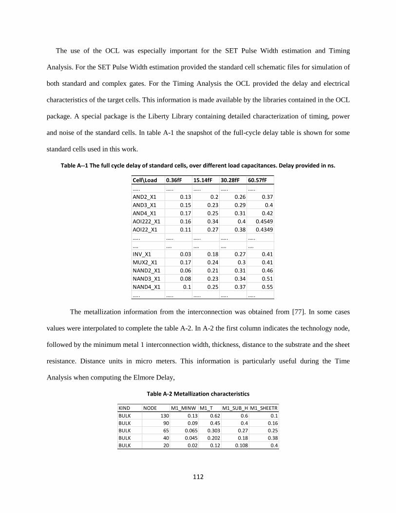
112
The use of the OCL was especially important for the SET Pulse Width estimation and Timing
Analysis. For the SET Pulse Width estimation provided the standard cell schematic files for simulation of
both standard and complex gates. For the Timing Analysis the OCL provided the delay and electrical
characteristics of the target cells. This information is made available by the libraries contained in the OCL
package. A special package is the Liberty Library containing detailed characterization of timing, power
and noise of the standard cells. In table A-1 the snapshot of the full-cycle delay table is shown for some
standard cells used in this work.
Table A--1 The full cycle delay of standard cells, over different load capacitances. Delay provided in ns.
The metallization information from the interconnection was obtained from [77]. In some cases
values were interpolated to complete the table A-2. In A-2 the first column indicates the technology node,
followed by the minimum metal 1 interconnection width, thickness, distance to the substrate and the sheet
resistance. Distance units in micro meters. This information is particularly useful during the Time
Analysis when computing the Elmore Delay,
Table A-2 Metallization characteristics
Cell\Load 0.36fF 15.14fF 30.28fF 60.57fF
….. ….. ….. ….. …..
AND2_X1 0.13 0.2 0.26 0.37
AND3_X1 0.15 0.23 0.29 0.4
AND4_X1 0.17 0.25 0.31 0.42
AOI222_X1 0.16 0.34 0.4 0.4549
AOI22_X1 0.11 0.27 0.38 0.4349
….. ….. ….. ….. …..
…. …. …. …. ….
INV_X1 0.03 0.18 0.27 0.41
MUX2_X1 0.17 0.24 0.3 0.41
NAND2_X1 0.06 0.21 0.31 0.46
NAND3_X1 0.08 0.23 0.34 0.51
NAND4_X1 0.1 0.25 0.37 0.55
….. ….. ….. ….. …..
KIND NODE M1_MINW M1_T M1_SUB_H M1_SHEETR
BULK 130 0.13 0.62 0.6 0.1
BULK 90 0.09 0.45 0.4 0.16
BULK 65 0.065 0.303 0.27 0.25
BULK 40 0.045 0.202 0.18 0.38
BULK 20 0.02 0.12 0.108 0.4

113
Flip flop information required for both Time De-rating calculation and the Timing Closure
estimation are shown in table A-3. The delay data from Setup Time and Hold Time refer to the full cycle
delay, and is given in nano seconds. The Flip Flop Leakage is given in nano Watts.
Table A--3 Flip Flop Technology Information
The analysis over the benchmarks to be presented in the next section have indicated the standard cells to
be used in this work, and shown in table A-4. Information regarding the number of transistors, cell width
and cell height are shown for reference.
Table A--4 - OCL Cells used by the benchmarks
[45nm]
Standard Cells Transistors W(um) H(um) Area(um2) INV_X1 2 0.61 1.63 0.9943
INV_X2 4 0.8 1.63 1.304
INV_X4 8 1.18 1.63 1.9234
INV_X8 16 1.94 1.63 3.1622 INV_X16 32 3.46 1.63 5.6398
BUF_X1 4 0.8 1.63 1.304 NAND2_X1 4 0.8 1.63 1.304 NAND3_X1 6 0.99 1.63 1.6137
NAND4_X1 8 1.18 1.63 1.9234 NAND2_X2 8 1.18 1.63 1.9234
NAND3_X2 12 1.56 1.63 2.5428 NAND4_X2 16 1.94 1.63 3.1622 AND2_X1 6 0.99 1.63 1.6137 AND3_X1 8 1.18 1.63 1.9234
AND4_X1 10 1.37 1.63 2.2331 NOR2_X1 4 0.8 1.63 1.304 NOR3_X1 6 0.99 1.63 1.6137
NOR4_X1 8 1.18 1.63 1.9234 NOR2_X2 8 1.18 1.63 1.9234 NOR3_X2 12 1.56 1.63 2.5428 NOR4_X2 16 1.94 1.63 3.1622 OR2_X1 6 0.99 1.63 1.6137 OR3_X1 8 1.18 1.63 1.9234
KIND NODE FF_SETUP_TIME FF_HOLD_TIME FF_LEAKAGE
BULK 130 0.1 0.11 175.21
BULK 90 0.09 0.1 144.14
BULK 65 0.058 0.065 110.1
BULK 40 0.035 0.04 79.11
BULK 20 0.02 0.015 49.44
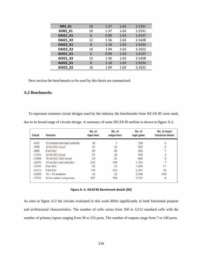
114
OR4_X1 10 1.37 1.63 2.2331 XOR2_X1 10 1.37 1.63 2.2331
OAI21_X1 6 0.99 1.63 1.6137 OAI21_X2 12 1.56 1.63 2.5428 OAI22_X1 8 1.18 1.63 1.9234 OAI22_X2 16 1.94 1.63 3.1622 AOI21_X1 6 0.99 1.63 1.6137
AOI21_X2 12 1.56 1.63 2.5428 AOI22_X1 8 1.18 1.63 1.9234 AOI22_X2 16 1.94 1.63 3.1622
Next section the benchmarks to be used by this thesis are summarized.
A.2 Benchmarks
To represent common circuit designs used by the industry the benchmarks from ISCAS 85 were used,
due to its broad range of circuits design. A summary of some ISCAS 85 netlists is shown in figure A-2.
Figure A--2- ISCAS'85 Benchmark details [83]
As seen in figure A-2 the circuits evaluated in this work differ significantly in both functional purpose
and architectural characteristics. The number of cells varies from 160 to 3,512 standard cells with the
number of primary inputs ranging from 36 to 233 ports. The number of outputs range from 7 to 140 ports.
115
Publications
List of Publications
Journals
1. T.R. Assis, K. Ni, J. Kauppila, B. L. Bhuva, R.D. Schrimpf, L.W. Massengill, S. Wen, R. Wong, C.
Slayman. Estimation of Single-Event Induced Collected Charge for Multiple Transistors Using
Analytical Expressions. IEEE Transactions on Nuclear Science. 2015.
2. J.S. Kauppila, W.H. Kay, T.D. Haeffner, D.R. Rauch, T.R. Assis, N.N Mahatme, J. Gaspard, B.L. Bhuva,
M.L. Alles, W.T. Holman, L.W. Massengill. “Single-Event Upset Characterization Across
Temperature and Supply Voltage for a 20nm Bulk Planar CMOS Technology” IEEE Transactions on
Nuclear Science. 2015
3. N. A. Dodds, M. J. Martinez, P. E. Dodd, M. R. Shaneyfelt, F. W. Sexton, J. D. Black, D. S. Lee, S. E.
Swanson,B. L. Bhuva, K. M. Warren, R. A. Reed, J. Trippe, B. D. Sierawski, R. A. Weller, N. Mahatme,
N. J. Gaspard, T. Assis, R. Austin, S. L. Weeden-Wright, L. W. Massengill, G. Swift, M. Wirthlin, M.
Cannon, R. Liu, L. Chen, A. T. Kelly, P. W. Marshall, M. Trinczek, E. W. Blackmore, S.-J. Wen, R. Wong,
B. Narasimham, J. A. Pellish, and H. Puchner. “The contribution of low-energy protons to the total on-
orbit SEU rate”. IEEE Transactions on Nuclear Science. 2015.
4. Mahatme, N.N.; Gaspard, N.J.; Assis, T.; Chatterjee, I.; Loveless, T.D.; Bhuva, B.L.; Robinson, W.H.;
Massengill, L.W.; Wen, S.-J.; Wong, R., "Kernel-Based Circuit Partition Approach to Mitigate
Combinational Logic Soft Errors,"Nuclear Science, IEEE Transactions on , vol.61, no.6, pp.3274,3281,
Dec. 2014
5. Jagannathan, S.; Loveless, T. D.; Bhuva, B. L.; Gaspard, N. J.; Mahatme, N.; Assis, T.; Wen, S.-J.; Wong,
R.; Massengill, L. W.; Frequency Dependence of Alpha-Particle Induced Soft Error Rates of Flip-
Flops in 40-nm CMOS Technology. Nuclear Science, IEEE Transactions on , Volume 59 (6), Dec 1,
2012.
Conferences
1. T.R. Assis, K. Ni, J. Kauppila, B. L. Bhuva, R.D. Schrimpf, L.W. Massengill, S. Wen, R. Wong, C.
Slayman. Estimation of Single-Event Induced Collected Charge for Multiple Transistors Using
Analytical Expressions. IEEE Nuclear and Space Radiation Effects Conference 2015.
2. T.R. Assis, N. J. Gaspard, N. N. Mahatme, R. A. Reed, R. A. Weller, M. H. Mendenhall, B. L. Bhuva, L.
W. Massengill, E. Blackmore, M. Trinczek, S. A. Wender. Neutrons and Protons Radiation Induced
Single Event Effects in an Advanced Technology Node. Single Event Effects (SEE) Symposium, May.
2014.
3. Mahatme, N.N.; Gaspard, N.J.; Assis, T.; Jagannathan, S.; Chatterjee, I.; Loveless, T.D.; Bhuva, B.L.;
Massengill, L.W.; Wen, S.J.; Wong, R., "Impact of technology scaling on the combinational logic soft
error rate," Reliability Physics Symposium, 2014 IEEE International , vol., no., pp.5F.2.1,5F.2.6, 1-5 June
2014
4. Narasimham, B.; Chandrasekharan, K.; Wang, J.K.; Djaja, G.; Gaspard, N.J.; Mahatme, N.N.; Assis, T.R.;
Bhuva, B.L., "High-speed pulsed-hysteresis-latch design for improved SER performance in 20 nm
bulk CMOS process,"Reliability Physics Symposium, 2014 IEEE International , vol., no.,
pp.5F.4.1,5F.4.5, 1-5 June 2014
5. Adrian Evans (Cisco), Michael Nicolaidis (IMAG-FR), Shi-Jie Wen(Cisco), Thiago Assis(Vanderbilt) B.
Bhuva (Vanderbilt). Clustering Techniques and Statistical Fault Injection for Selective Mitigation of
SEUs in Flip-Flops. International Symposium on Quality Electronic Design (ISQED) 2013

116
Industry Awards\Competitions
1. Cisco Systems - 1st Place Supply Chain Operation Case Competition – 2014
2. Cisco Systems - 1st Place Supply Chain Operation Case Competition – 2013