bruce mayer, pe licensed electrical & mechanical engineer bmayer@chabotcollege
DESCRIPTION
Engineering 45. Imperfections In Solids. Bruce Mayer, PE Licensed Electrical & Mechanical Engineer [email protected]. Learning Goals. Learn The Forms of Defects in Solids Use metals as Prototypical Example How the number and type of defects Can be varied and controlled - PowerPoint PPT PresentationTRANSCRIPT
[email protected] • ENGR-45_Lec-05_SolidImperfections.ppt1
Bruce Mayer, PE Engineering-45: Materials of Engineering
Bruce Mayer, PELicensed Electrical & Mechanical Engineer
Engineering 45
ImperfectioImperfectionsns
In SolidsIn Solids
[email protected] • ENGR-45_Lec-05_SolidImperfections.ppt2
Bruce Mayer, PE Engineering-45: Materials of Engineering
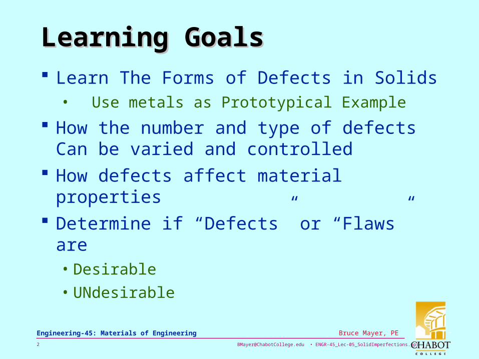
Learning GoalsLearning Goals
Learn The Forms of Defects in Solids• Use metals as Prototypical Example
How the number and type of defects Can be varied and controlled
How defects affect material properties Determine if “Defects” or “Flaws” are
• Desirable
• UNdesirable
[email protected] • ENGR-45_Lec-05_SolidImperfections.ppt3
Bruce Mayer, PE Engineering-45: Materials of Engineering
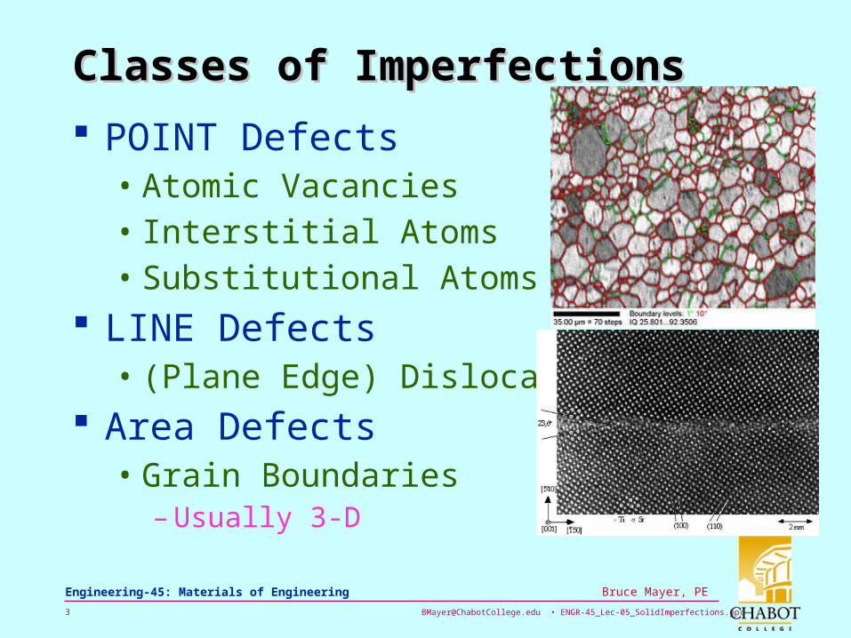
Classes of ImperfectionsClasses of Imperfections
POINT Defects• Atomic Vacancies• Interstitial Atoms• Substitutional Atoms
LINE Defects• (Plane Edge) Dislocations
Area Defects• Grain Boundaries
– Usually 3-D
[email protected] • ENGR-45_Lec-05_SolidImperfections.ppt4
Bruce Mayer, PE Engineering-45: Materials of Engineering
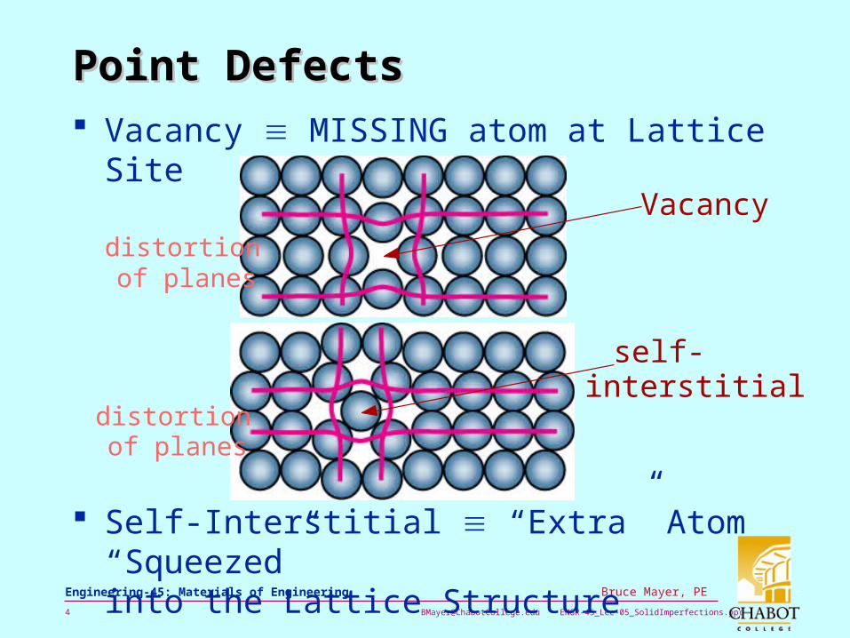
Point DefectsPoint Defects Vacancy MISSING atom at Lattice Site
Self-Interstitial “Extra” Atom “Squeezed” into the Lattice Structure
Vacancydistortion of planes
self-interstitial
distortion of planes
[email protected] • ENGR-45_Lec-05_SolidImperfections.ppt5
Bruce Mayer, PE Engineering-45: Materials of Engineering
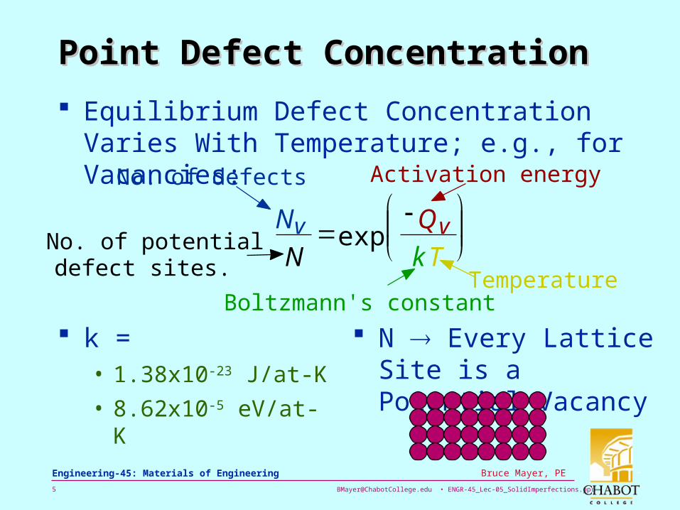
Point Defect ConcentrationPoint Defect Concentration
Equilibrium Defect Concentration Varies With Temperature; e.g., for Vacancies:
k = • 1.38x10⁻²³ J/at-K
• 8.62x10⁻⁵ eV/at-K
N Every Lattice Site is a Potential Vacancy
Boltzmann's constant
Nv
Nexp
Qv
kT
No. of defects
No. of potential defect sites.
Activation energy
Temperature
[email protected] • ENGR-45_Lec-05_SolidImperfections.ppt6
Bruce Mayer, PE Engineering-45: Materials of Engineering
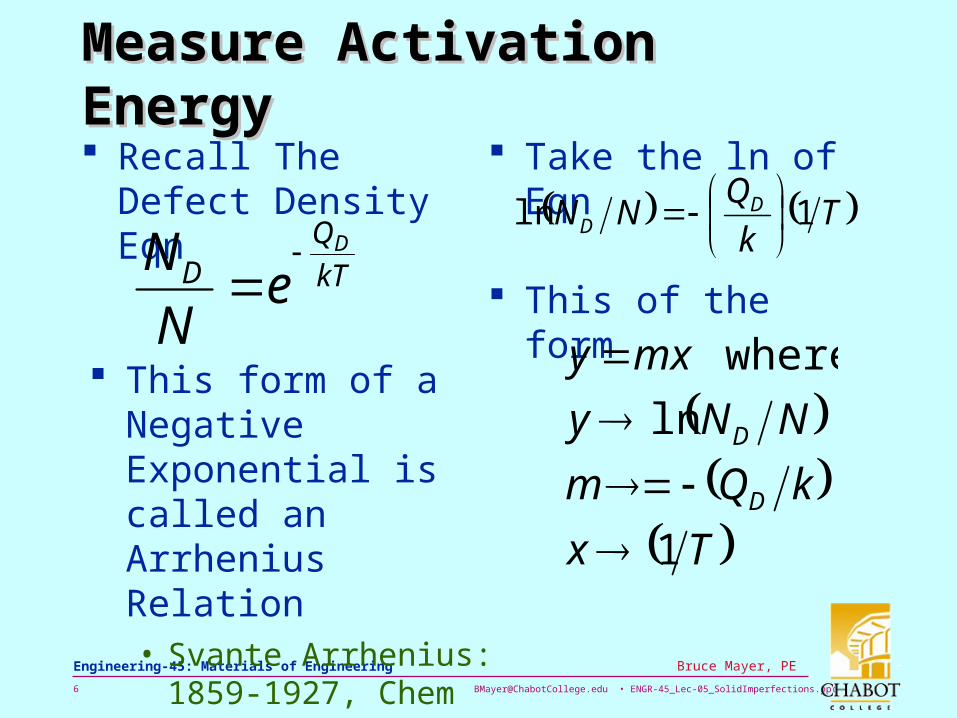
Measure Activation EnergyMeasure Activation Energy Recall The Defect
Density Eqn Take the ln of Eqn
kT
QD
D
eN
N
This form of a Negative Exponential is called an Arrhenius Relation• Svante Arrhenius:
1859-1927, Chem Nobel 1903
Tk
QNN D
D 1ln
This of the form
Tx
kQm
NNy
mxy
D
D
1
ln
where
[email protected] • ENGR-45_Lec-05_SolidImperfections.ppt7
Bruce Mayer, PE Engineering-45: Materials of Engineering
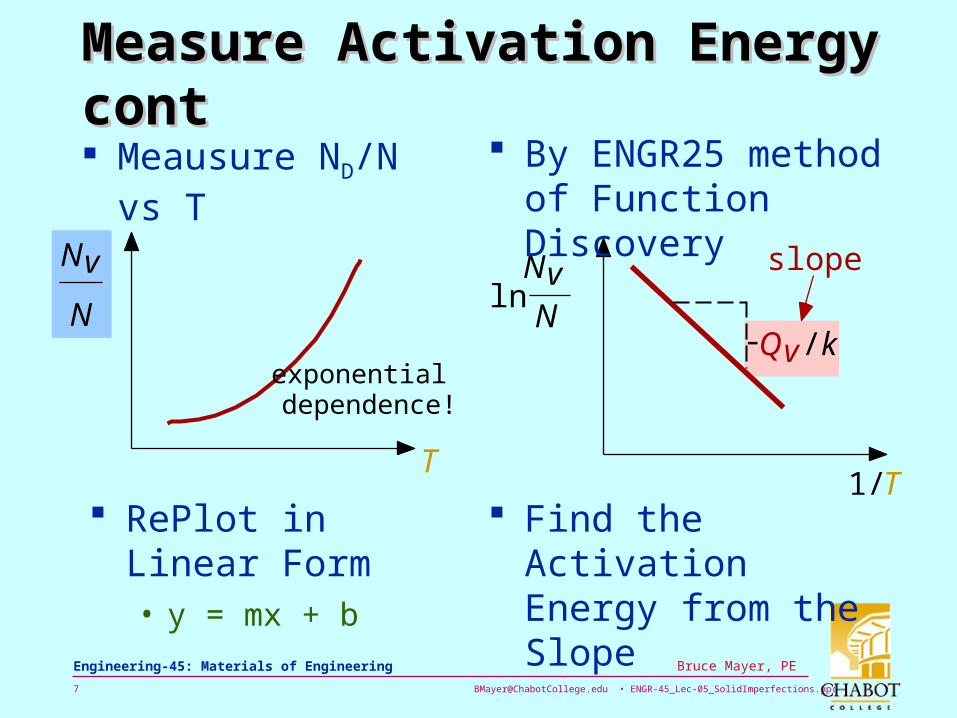
Measure Activation Energy contMeasure Activation Energy cont Meausure ND/N vs T
Find the Activation Energy from the Slope
RePlot in Linear Form• y = mx + b
Nv
N
T
exponential dependence!
1/T
N
Nvln
-Qv /k
slope
By ENGR25 method of Function Discovery

[email protected] • ENGR-45_Lec-05_SolidImperfections.ppt8
Bruce Mayer, PE Engineering-45: Materials of Engineering
Vacancy Concentration ExmplVacancy Concentration Exmpl In Defect Density
Rln QD Can Take Two forms• Qv Vacancies
• Qi Interstitials
Consider a Qv Case
• Copper at 1000 C
• Qv = 0.9 eV/at
• ACu = 63.5 g/mol
= 8400 kg/cu-m
Find the Vacancy Density• First Find N in units
of atoms per cu-m
3
3
23
//
Check units
0635.0
840010023.6
m
at
molkg
mkgmolatN
N
A
NN
Cu
A
[email protected] • ENGR-45_Lec-05_SolidImperfections.ppt9
Bruce Mayer, PE Engineering-45: Materials of Engineering
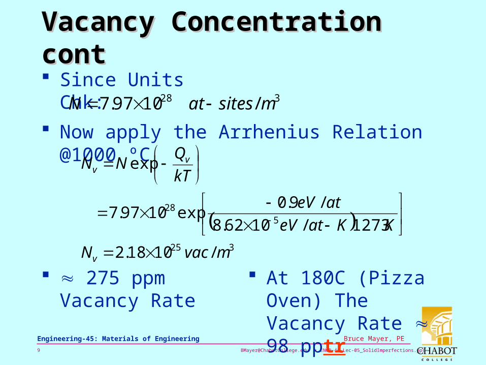
Vacancy Concentration contVacancy Concentration cont Since Units Chk:
At 180C (Pizza Oven) The Vacancy Rate 98 pptr
328 /1097.7 msitesatN Now apply the Arrhenius Relation @1000 ºC
275 ppm Vacancy Rate
325
528
/1018.2
1273/1062.8
/9.0exp1097.7
exp
mvacN
KKateV
ateV
kT
QNN
v
vv
[email protected] • ENGR-45_Lec-05_SolidImperfections.ppt10
Bruce Mayer, PE Engineering-45: Materials of Engineering
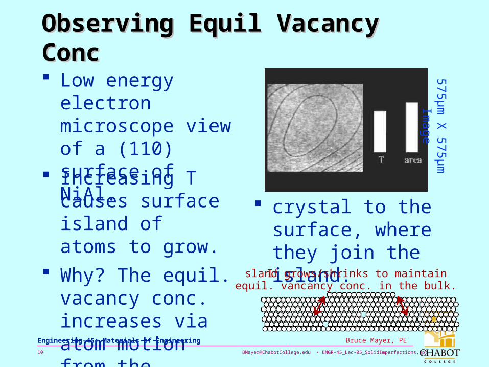
Observing Equil Vacancy ConcObserving Equil Vacancy Conc
Low energy electron microscope view of a (110) surface of NiAl.
Increasing T causes surface island of atoms to grow.
Why? The equil. vacancy conc. increases via atom motion from the
crystal to the surface, where they join the island.
575
μm
X 5
75
μm
Im
age
Island grows/shrinks to maintain equil. vancancy conc. in the bulk.

[email protected] • ENGR-45_Lec-05_SolidImperfections.ppt11
Bruce Mayer, PE Engineering-45: Materials of Engineering
Point Impurities in SolidsPoint Impurities in Solids Two outcomes if impurity (B) added to host (A)
1. Solid solution of B in A (i.e., random dist. of point defects)
2. Solid solution of B in A plus particles of a NEW PHASE (usually for a larger amount of B)
OR
Substitutional alloy(e.g., Cu in Ni)
Interstitial alloy
(e.g., C in Fe)
Second phase particle• different composition (chem formula)• often different structure
• e.g.; BCC in FCC
[email protected] • ENGR-45_Lec-05_SolidImperfections.ppt12
Bruce Mayer, PE Engineering-45: Materials of Engineering
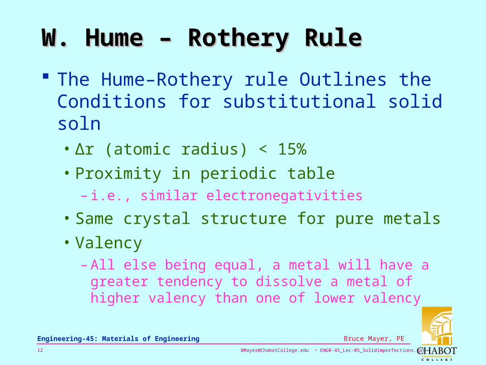
W. Hume – Rothery RuleW. Hume – Rothery Rule
The Hume–Rothery rule Outlines the Conditions for substitutional solid soln• Δr (atomic radius) < 15%
• Proximity in periodic table – i.e., similar electronegativities
• Same crystal structure for pure metals
• Valency– All else being equal, a metal will have a greater
tendency to dissolve a metal of higher valency than one of lower valency
[email protected] • ENGR-45_Lec-05_SolidImperfections.ppt13
Bruce Mayer, PE Engineering-45: Materials of Engineering
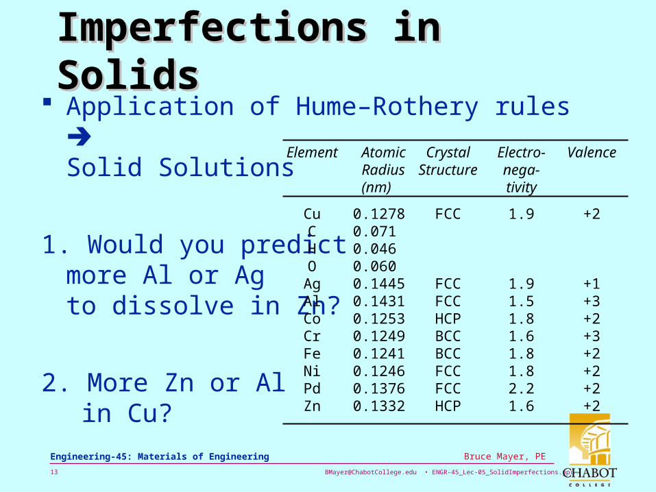
Imperfections in SolidsImperfections in Solids Application of Hume–Rothery rules
Solid Solutions
1. Would you predictmore Al or Ag to dissolve in Zn?
2. More Zn or Al in Cu?
Element Atomic Crystal Electro- ValenceRadius Structure nega-
(nm) tivity
Cu 0.1278 FCC 1.9 +2C 0.071H 0.046O 0.060Ag 0.1445 FCC 1.9 +1Al 0.1431 FCC 1.5 +3Co 0.1253 HCP 1.8 +2Cr 0.1249 BCC 1.6 +3Fe 0.1241 BCC 1.8 +2Ni 0.1246 FCC 1.8 +2Pd 0.1376 FCC 2.2 +2Zn 0.1332 HCP 1.6 +2
[email protected] • ENGR-45_Lec-05_SolidImperfections.ppt14
Bruce Mayer, PE Engineering-45: Materials of Engineering
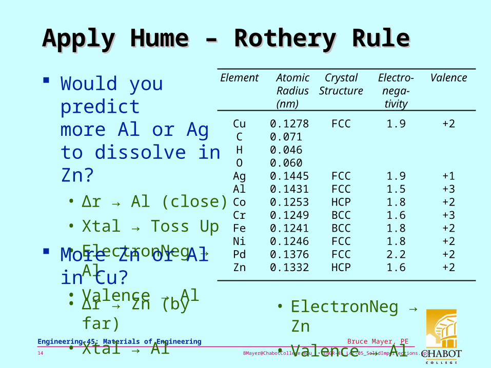
Apply Hume – Rothery RuleApply Hume – Rothery Rule
Would you predictmore Al or Ag to dissolve in Zn? • Δr → Al (close)
• Xtal → Toss Up
• ElectronNeg → Al
• Valence → Al
Element Atomic Crystal Electro- ValenceRadius Structure nega-
(nm) tivity
Cu 0.1278 FCC 1.9 +2C 0.071H 0.046O 0.060Ag 0.1445 FCC 1.9 +1Al 0.1431 FCC 1.5 +3Co 0.1253 HCP 1.8 +2Cr 0.1249 BCC 1.6 +3Fe 0.1241 BCC 1.8 +2Ni 0.1246 FCC 1.8 +2Pd 0.1376 FCC 2.2 +2Zn 0.1332 HCP 1.6 +2
More Zn or Al in Cu?• Δr → Zn (by far)
• Xtal → Al
• ElectronNeg → Zn
• Valence → Al
[email protected] • ENGR-45_Lec-05_SolidImperfections.ppt15
Bruce Mayer, PE Engineering-45: Materials of Engineering
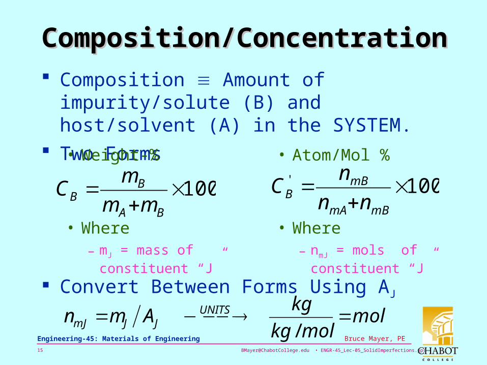
Composition/ConcentrationComposition/Concentration Composition Amount of impurity/solute (B)
and host/solvent (A) in the SYSTEM. Two Forms
Convert Between Forms Using AJ
• Weight-%
• Where– mJ = mass of
constituent “J”
100'
mBmA
mBB nn
nC
• Atom/Mol %
• Where– nmJ = mols of
constituent “J”
molmolkg
kgAmn UNITSJJmJ
/
100
BA
BB mm
mC
[email protected] • ENGR-45_Lec-05_SolidImperfections.ppt16
Bruce Mayer, PE Engineering-45: Materials of Engineering
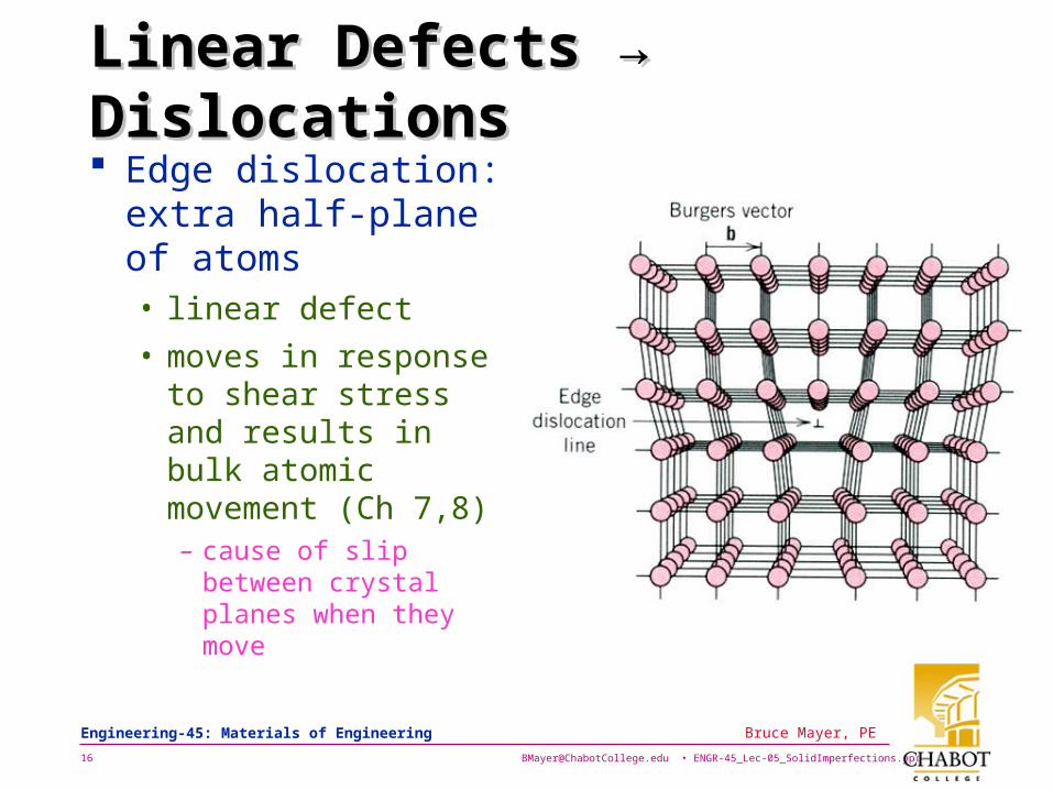
Linear Defects → DislocationsLinear Defects → Dislocations Edge dislocation:
extra half-plane of atoms• linear defect
• moves in response to shear stress and results in bulk atomic movement (Ch 7,8)– cause of slip between
crystal planes when they move
[email protected] • ENGR-45_Lec-05_SolidImperfections.ppt17
Bruce Mayer, PE Engineering-45: Materials of Engineering
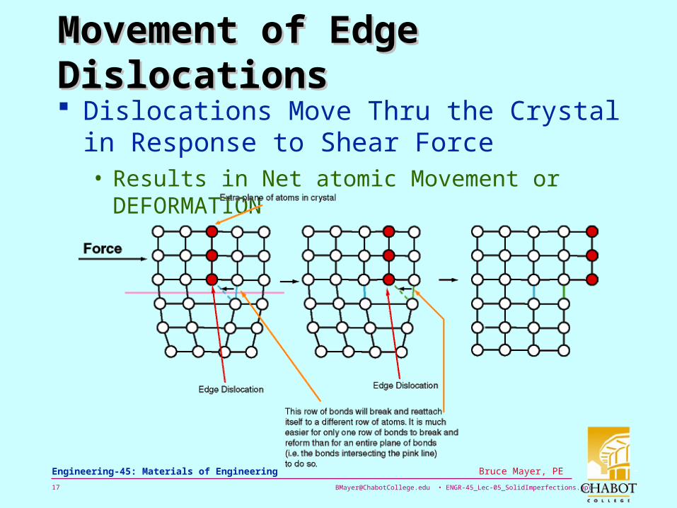
Movement of Edge DislocationsMovement of Edge Dislocations Dislocations Move Thru the Crystal in
Response to Shear Force• Results in Net atomic Movement or DEFORMATION
[email protected] • ENGR-45_Lec-05_SolidImperfections.ppt18
Bruce Mayer, PE Engineering-45: Materials of Engineering
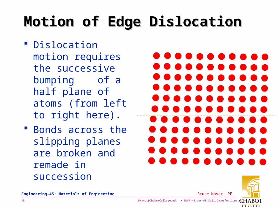
Motion of Edge DislocationMotion of Edge Dislocation
Dislocation motion requires the successive bumping of a half plane of atoms (from left to right here).
Bonds across the slipping planes are broken and remade in succession
[email protected] • ENGR-45_Lec-05_SolidImperfections.ppt19
Bruce Mayer, PE Engineering-45: Materials of Engineering
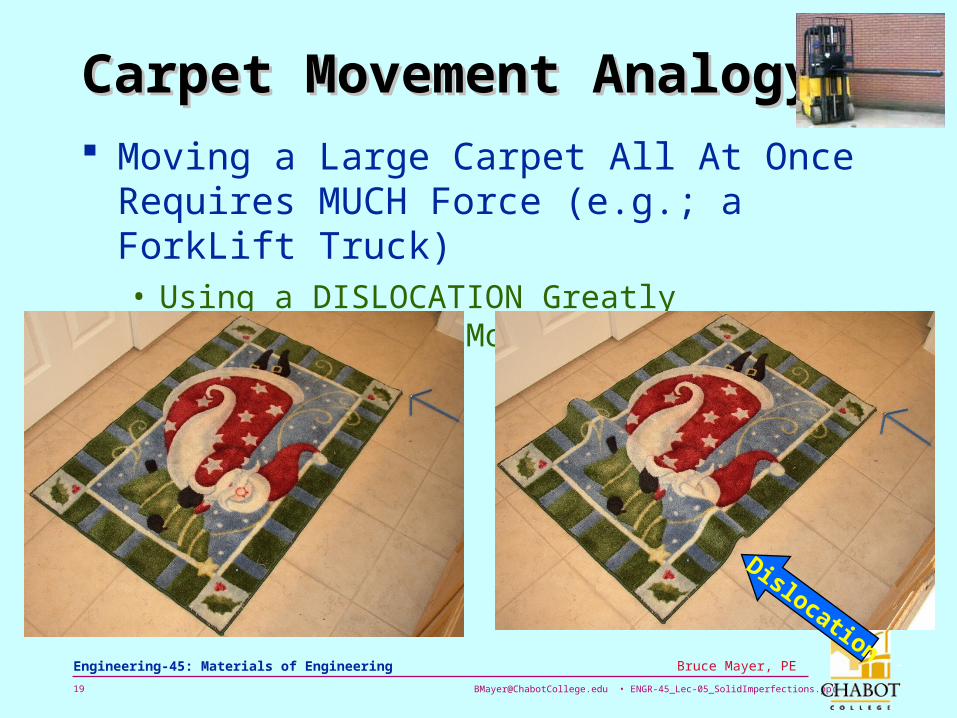
Carpet Movement AnalogyCarpet Movement Analogy Moving a Large Carpet All At Once Requires
MUCH Force (e.g.; a ForkLift Truck)• Using a DISLOCATION Greatly Facilitates the Move
Dislocation
[email protected] • ENGR-45_Lec-05_SolidImperfections.ppt20
Bruce Mayer, PE Engineering-45: Materials of Engineering
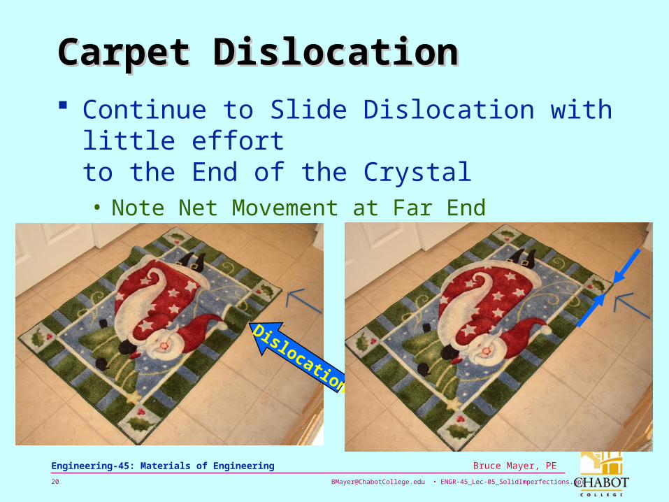
Carpet DislocationCarpet Dislocation Continue to Slide Dislocation with little effort
to the End of the Crystal• Note Net Movement at Far End
Dislocation
[email protected] • ENGR-45_Lec-05_SolidImperfections.ppt21
Bruce Mayer, PE Engineering-45: Materials of Engineering
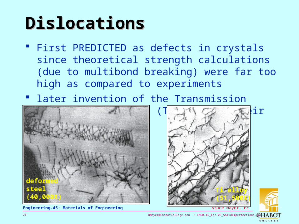
DislocationsDislocations First PREDICTED as defects in crystals since
theoretical strength calculations (due to multibond breaking) were far too high as compared to experiments
later invention of the Transmission Electron Microscope (TEM) PROVED their Existence
deformed steel (40,000X)
Ti alloy (51,500X)
[email protected] • ENGR-45_Lec-05_SolidImperfections.ppt22
Bruce Mayer, PE Engineering-45: Materials of Engineering
Interfacial DefectsInterfacial Defects
2D, Sheet-like Defects are Termed as Interfacial
Some Macro-Scale Examples• Solid Surfaces (Edges)
– Bonds of Surface Atoms are NOT SatisfiedSource of “Surface Energy” in Units of J/sq-m
• Stacking Faults – When atom-Plane Stacking Pattern is Not as Expected
• Phase Boundaries – InterFace Between Different Xtal Structures

[email protected] • ENGR-45_Lec-05_SolidImperfections.ppt23
Bruce Mayer, PE Engineering-45: Materials of Engineering
Interface Def. → Grain BoundariesInterface Def. → Grain Boundaries
Grain Boundaries• are Boundaries BETWEEN crystals
• Produced by the solidification process, for example
• Have a Change In Crystal Orientation across them
• IMPEDE dislocation motion
• Generally Weaker that the Native Xtal– Typically Reduce Material Strength
thru Grain-Boundary Tearing
Crack Along GB
[email protected] • ENGR-45_Lec-05_SolidImperfections.ppt24
Bruce Mayer, PE Engineering-45: Materials of Engineering
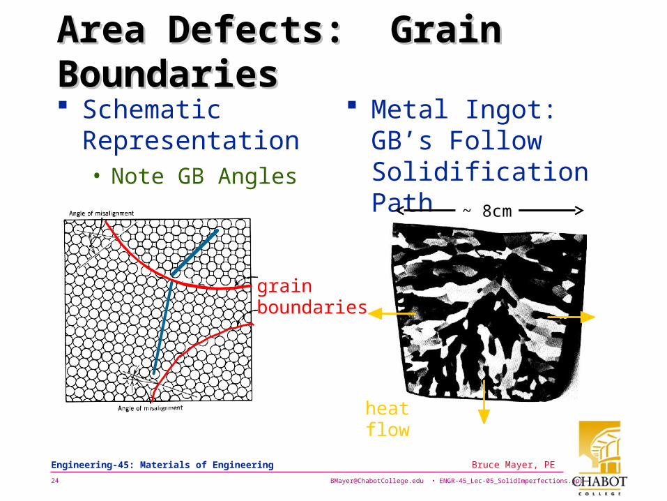
Area Defects: Grain BoundariesArea Defects: Grain Boundaries Schematic
Representation• Note GB Angles
grain boundaries
Metal Ingot: GB’s Follow Solidification Path
heat flow
~ 8cm
[email protected] • ENGR-45_Lec-05_SolidImperfections.ppt25
Bruce Mayer, PE Engineering-45: Materials of Engineering
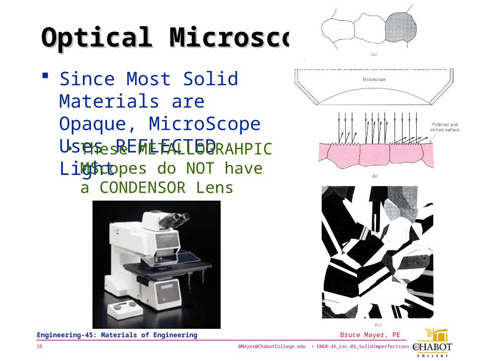
Optical MicroscopyOptical Microscopy Since Most Solid Materials
are Opaque, MicroScope Uses REFLECTED Light• These METALLOGRAHPIC
MScopes do NOT have a CONDENSOR Lens

[email protected] • ENGR-45_Lec-05_SolidImperfections.ppt26
Bruce Mayer, PE Engineering-45: Materials of Engineering
Optical MicroScopy contOptical MicroScopy cont The Resolution, Z The Magnification, M
NAZ
61.0
• Where Light Wavelength
550 nm For “White” Light (Green Ctr)
– NA Numerical Aperture for the OBJECTIVE Lens 0.9 for a Very
High Quality Lens
Typical Values• Z 375 nm
– Objects Smaller than This Cannot be observed
– Objects Closer Together than This Cannot Be Separated
• Mtrue 200
mmtrue
NAM
12.0
[email protected] • ENGR-45_Lec-05_SolidImperfections.ppt27
Bruce Mayer, PE Engineering-45: Materials of Engineering
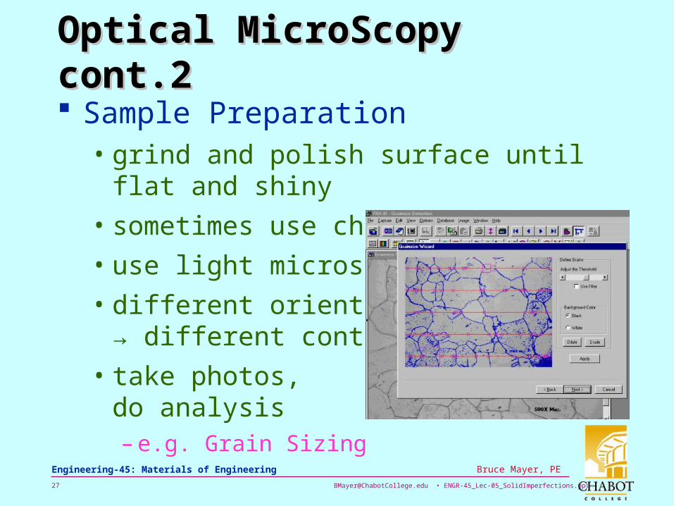
Optical MicroScopy cont.2Optical MicroScopy cont.2
Sample Preparation• grind and polish surface until flat and shiny
• sometimes use chemical etch
• use light microscope
• different orientations → different contrast
• take photos, do analysis– e.g. Grain Sizing
[email protected] • ENGR-45_Lec-05_SolidImperfections.ppt28
Bruce Mayer, PE Engineering-45: Materials of Engineering
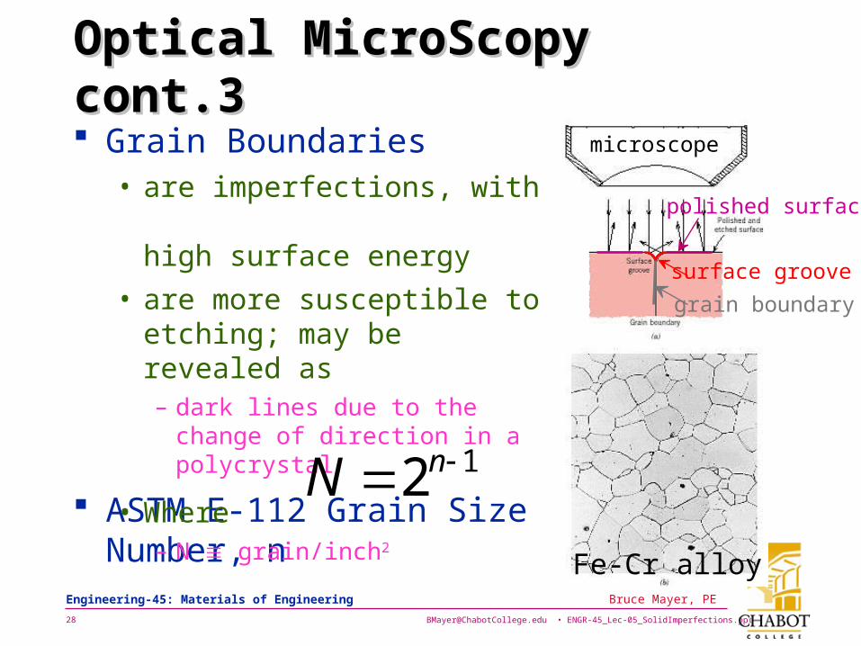
Optical MicroScopy cont.3Optical MicroScopy cont.3 Grain Boundaries
• are imperfections, with high surface energy
• are more susceptible to etching; may be revealed as – dark lines due to the change of
direction in a polycrystal
ASTM E-112 Grain Size Number, n 12 nN• Where
– N grain/inch2
microscope
grain boundary
surface groove
polished surface
Fe-Cr alloy
[email protected] • ENGR-45_Lec-05_SolidImperfections.ppt29
Bruce Mayer, PE Engineering-45: Materials of Engineering
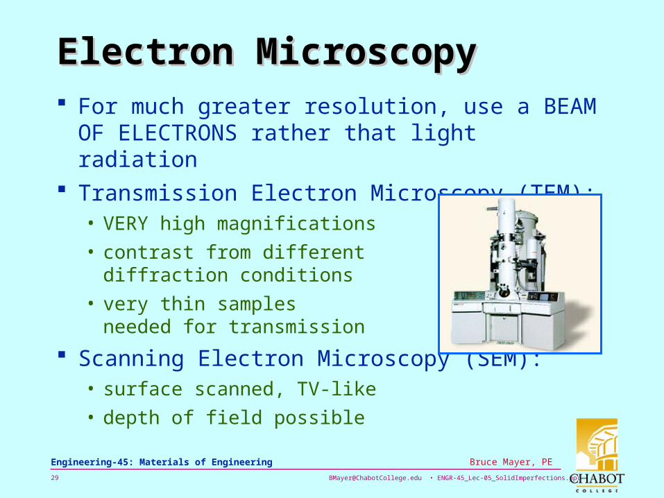
Electron MicroscopyElectron Microscopy For much greater resolution, use a BEAM OF
ELECTRONS rather that light radiation Transmission Electron Microscopy (TEM):
• VERY high magnifications
• contrast from different diffraction conditions
• very thin samples needed for transmission
Scanning Electron Microscopy (SEM):• surface scanned, TV-like
• depth of field possible

[email protected] • ENGR-45_Lec-05_SolidImperfections.ppt30
Bruce Mayer, PE Engineering-45: Materials of Engineering
Atomic Force MicroScopy Atomic Force MicroScopy AFM is Also called Scanning
Probe Microscopy (SPM)• tiny probe with a tinier tip
rasters across the surface
• topographical map on atomic scale
Polymer
[email protected] • ENGR-45_Lec-05_SolidImperfections.ppt31
Bruce Mayer, PE Engineering-45: Materials of Engineering
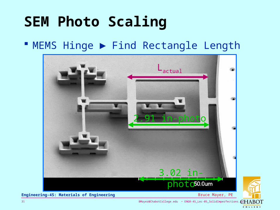
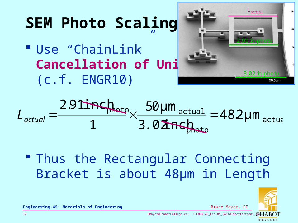
SEM Photo Scaling
MEMS Hinge ► Find Rectangle Length
3.02 in-photo
2.91 in-photo
Lactual
[email protected] • ENGR-45_Lec-05_SolidImperfections.ppt32
Bruce Mayer, PE Engineering-45: Materials of Engineering
SEM Photo Scaling
Use “ChainLink” Cancellation of Units (c.f. ENGR10)
Thus the Rectangular Connecting Bracket is about 48µm in Length
actualphoto
actualphoto µm 2.48inch .023
µm 05
1
inch 91.2actualL
3.02 in-photo
2.91 in-photo
Lactual
[email protected] • ENGR-45_Lec-05_SolidImperfections.ppt33
Bruce Mayer, PE Engineering-45: Materials of Engineering
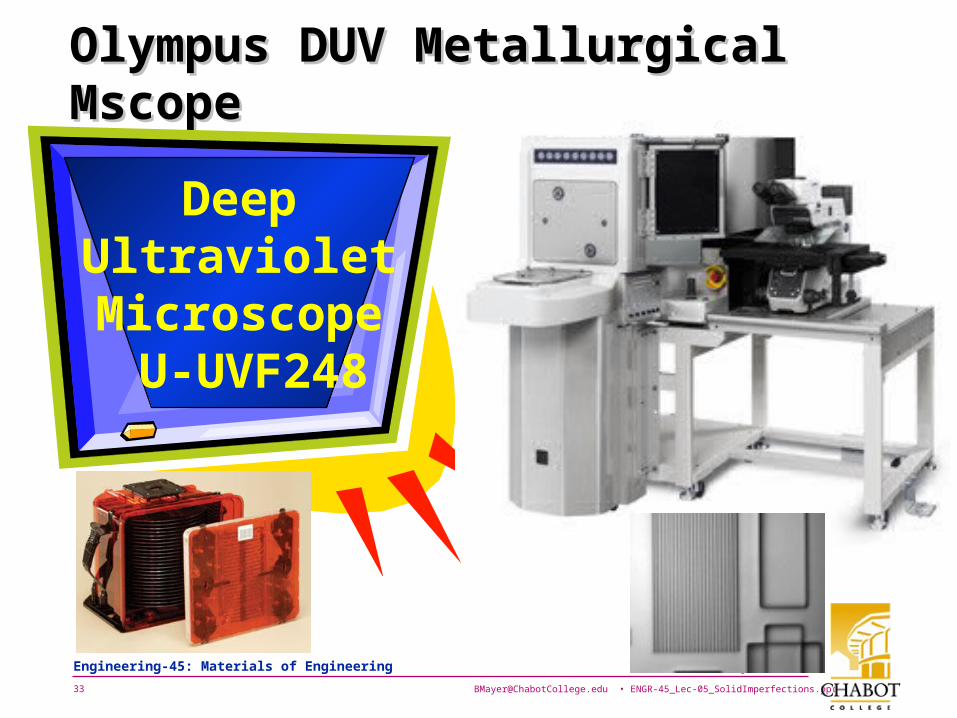
Olympus DUV Metallurgical MscopeOlympus DUV Metallurgical Mscope
DeepUltravioletMicroscope U-UVF248