banafsheh barabadi multiscale transient thermal analysis...
TRANSCRIPT

Banafsheh BarabadiDepartment of Mechanical Engineering,
Massachusetts Institute of Technology,
77 Massachusetts Avenue,
Cambridge, MA 02139
Satish KumarGeorge W. Woodruff School
of Mechanical Engineering,
Georgia Institute of Technology,
801 Ferst Drive,
Atlanta, GA 30332
Valeriy SukharevDesign-to-Silicon,
Mentor Graphics Corporation,
46871 Bayside Parkway,
Fremont, CA 94538
Yogendra K. Joshi1George W. Woodruff School
of Mechanical Engineering,
Georgia Institute of Technology,
801 Ferst Drive,
Atlanta, GA 30332
e-mail: [email protected]
Multiscale Transient ThermalAnalysis of MicroelectronicsIn a microelectronic device, thermal transport needs to be simulated on scales rangingfrom tens of nanometers to hundreds of millimeters. High accuracy multiscale models arerequired to develop engineering tools for predicting temperature distributions with suffi-cient accuracy in such devices. A computationally efficient and accurate multiscalereduced order transient thermal modeling methodology was developed using a combina-tion of two different approaches: “progressive zoom-in” method and “proper orthogonaldecomposition (POD)” technique. The capability of this approach in handling severaldecades of length scales from “package” to “chip components” at a considerably lowercomputational cost, while maintaining satisfactory accuracy was demonstrated. A flipchip ball grid array (FCBGA) package was considered for demonstration. The transienttemperature and heat fluxes calculated on the top and bottom walls of the embedded chipat the package level simulations are employed as dynamic boundary conditions for thechip level simulation. The chip is divided into ten function blocks. Randomly generateddynamic power sources are applied in each of these blocks. The temperature rise in thedifferent layers of the chip calculated from the multiscale model is compared with a finiteelement (FE) model. The close agreement between two models confirms that the multi-scale approach can predict temperature rise accurately for scenarios corresponding todifferent power sources in functional blocks, without performing detailed FE simulations,which significantly reduces computational effort. [DOI: 10.1115/1.4029835]
Keywords: Joule heating, three-dimensional (3D) architecture, transient thermalanalysis, reduced order modeling, proper orthogonal decomposition, progressive zoom-in approach
1 Introduction
The integrated circuits (IC) industry is driven by scaling tosmaller and higher performing devices to enable lower cost andhigher speed. However, major challenges exist in maintaining per-formance and reliability while facing fundamental scaling limita-tions. The current chip and package architectures are subjected tohigher density of the heat dissipating elements and elevated totalpower generation rates. This can result in local hot-spots that arelayout and/or workload dependent, leading to significant variationin the performance and leakage current of devices. Moreover,cyclic thermal events as a result of Joule heating in the metallicinterconnect and transistors can lead to fatigue failure, due to thethermal expansion coefficients mismatch among different materi-als in the device. Thus, it is essential to develop fast and accuratemultiscale models to calculate the thermal response of circuits foradvanced technology nodes.
Various approaches have been proposed in the literature forpredicting temperature distributions with sufficient accuracy inchips and packages [1,2]. Among these multiscale methodologies,the traditional bottom-up approaches are extensively used for tran-sient thermal modeling. Perhaps, the best known of this class ofmethods is the resistance–capacitance network, which is con-structed using thermal impedances [3,4]. The accuracy of themodels decreases for complex geometries, complex boundaryconditions, and nonlinearity in the heat conduction equation [5].
Another common bottom-up approach utilizes compact models,which can be finite volume (FV) or FE based. In a traditional FEor FV analysis, the domain is discretized in a way that each ele-ment is homogeneous. It can, however, have anisotropic thermalconductivity. Compact models do not require conventional bilin-ear rectangular or homogeneous elements and can have elements
comprising both metal and dielectric region. Some of the firstcompact modeling work was done by Kreuger and Bar-Cohen in1992 [6]. They modeled a chip package with a simplified resistornetwork and shorter simulation times. However, the network to-pography of compact models becomes complex with increase inmodel size, also potentially compromising the accuracy of themodel [7]. Another limitation of such compact models is the diffi-culty in handling fluid/solid interactions. In general, these bottom-up approaches have primarily addressed the steady-state Jouleheating in interconnects. However, pulsed currents and the result-ing transient heat conduction in interconnect arrays remain a keyconcern in the design for reliability for the next generation high-performance chips.
Top-down approaches are another category of multiscale ther-mal modeling in microelectronics. A recent approach is behav-ioral thermal modeling, which is a combination of the generalizedpencil-of-function (GPOF) [8,9] and subspace methods [10,11].GPOF was developed in the communications community to esti-mate poles of an electromagnetic system by solving a generalizedeigenvalue problem. These methods are mainly used for high-performance multicore microprocessor design. In general, theypotentially suffer from a lack of predictability problems. There-fore, there is a need for the development of a new thermal simula-tion methodology that overcomes the challenges faced by existingthermal models.
In this study, a novel, computationally efficient, and accuratemultiscale reduced order transient thermal modeling methodologyis developed, which comprises two parts: (1) progressive zoom-inand (2) POD. The analyses at various length scales are integratedvia the progressive zoom-in approach, which is illustrated inFig. 1 and will be further discussed in Sec. 2.2. POD is a robustand elegant method of data analysis that provides low-dimensional but accurate descriptions of a high-dimensional sys-tem. It was first introduced by Lumley [12] in the field of turbu-lence; Holmes et al. [13] provided a thorough summary forapplications of POD in various fields. As shown by Barabadi et al.[14], for any linear system, the method is capable of predicting
1Corresponding author.Contributed by the Electronic and Photonic Packaging Division of ASME for
publication in the JOURNAL OF ELECTRONIC PACKAGING. Manuscript received May 2,2013; final manuscript received February 16, 2015; published online April 16, 2015.Assoc. Editor: Amy Fleischer.
Journal of Electronic Packaging SEPTEMBER 2015, Vol. 137 / 031002-1Copyright VC 2015 by ASME
Downloaded From: https://electronicpackaging.asmedigitalcollection.asme.org/ on 07/27/2015 Terms of Use: http://asme.org/terms
transient temperature distribution regardless of the temporal orspatial dependence of the applied heat source. This feature pro-vides the ability to predict temperature distributions for arbitraryheat inputs, by using a smaller sample set of applied heat sourcesand power maps, resulting in considerably decreased simulationtime. Combining POD with the progressive zoom-in approach canfurther enhance the computational efficiency.
The proposed methodology has the capability of modeling sev-eral decades of length scale from package to “chip component”and potentially the “interconnect” (not included here) levels, at asignificantly lower computational cost than currently availablemethods. This characteristic of the method also applies for timescales from seconds down to microseconds, corresponding to vari-ous transient thermal events. The suggested approach provides theability to rapidly predict thermal responses under different powerinput patterns, based only on a few representative detailed simula-tions, while maintaining adequate spatial and temporal accuracy.
In this paper, an FCBGA package with an embedded die is con-sidered for thermal modeling. Random dynamic power distribu-tions were considered for the total chip power, as well as for thefunction blocks that compose the entire chip to demonstrate thecapability of the POD method. To validate this methodology, theresults were compared with an FE model developed in COMSOL
[15]. It is demonstrated that the computational time is reduced byat least two orders of magnitude at every step of modeling.
2 Hybrid Scheme for Multiscale Thermal Modeling
A hybrid scheme has been developed in this paper, which com-bines the implementation of POD and progressive zoom-inapproach, as summarized below.
2.1 Fundamentals of POD Method. POD offers an optimalset of basis functions, also known as POD modes, which areempirically determined from an ensemble of observations. Theseobservations are obtained either experimentally or from numericalsimulation, as in this study. The POD method characterizes andcaptures the overall behavior and complexity of a physical systemby using a reduced number of degrees-of-freedom. This results ina much lower computational cost than a full-field simulationmethod. The most remarkable characteristic of the POD is its opti-mality, i.e., it provides the most efficient way of capturing thedominant components of an infinite-dimensional process, withonly finite number of basis functions [13]. In developing the PODmodel, data sets are expanded for modal decomposition on empir-ically determined basis functions in a way that minimizes the leastsquare error between the true solution and the truncated represen-tation of the POD model. Therefore, it makes the POD method themost efficient method of capturing the dominant components of alarge-dimensional system with a finite number of modes [16,17].
In this technique, the temperature distribution is determinedfrom the expansion
Tðx; y; z; tÞ ¼ T0ðx; y; zÞ þXm
i¼1
biðtÞ/iðx; y; zÞ (1)
where T0 is the time average of temperature (i.e., the mean vectorof the observation matrix), ui(x, y, z) is the ith POD mode, andbi(t) is the ith POD coefficient [14]. A detailed procedure to gener-ate a two-dimensional (2D) POD based reduced order model isprovided in Ref. [14]. The primary steps to generate a POD basedreduced order model are outlined below:
(1) Generating the observation matrix.(2) Calculating basis functions (POD modes).(3) Calculating POD coefficients, bi.
As demonstrated in Ref. [14], the POD coefficients, bi, can bedetermined by solving the discretized matrix of coupled ordinarydifferential equations, Eq. (2), using the sixth-order Runge–Kuttamethod shown below:
Aij_bjðtÞ � BijbjðtÞ � ðcþ qÞi ¼ 0; i; j ¼ 1; 2; :::;m (2)
Coefficients Aij, Bij, ci, and qi in Eq. (2) were derived and pre-sented for 2D POD model in Ref. [14]. For this study, coefficientsin Eq. (2) were determined for 3D analysis as
Aij ¼ð
Xuj � uidX (3a)
Bij ¼ð
Xauj � r2uidX ¼ �
ðX
a@uj
@x� @ui
@xþ@uj
@y� @ui
@yþ@uj
@z� @ui
@z
� �dX
þð
x
auj �@ui
@y
� �y¼ymax
y¼ymin
dxþð
y
auj �@ui
@x
� �x¼xmax
x¼xmin
dyþð
z
auj �@ui
@z
� �z¼zmax
z¼zmin
dx
(3b)
cj ¼ð
Xauj � r2T0dX ¼ �
ðX
a@uj
@x� @T0
@xþ@uj
@y� @T0
@yþ@uj
@z� @T0
@z
� �dX
þð
x
auj �@T0
@y
� �y¼ymax
y¼ymin
dxþð
y
auj �@T0
@x
� �x¼xmax
x¼xmin
dyþð
z
auj �@T0
@z
� �z¼zmax
z¼zmin
dz
(3c)
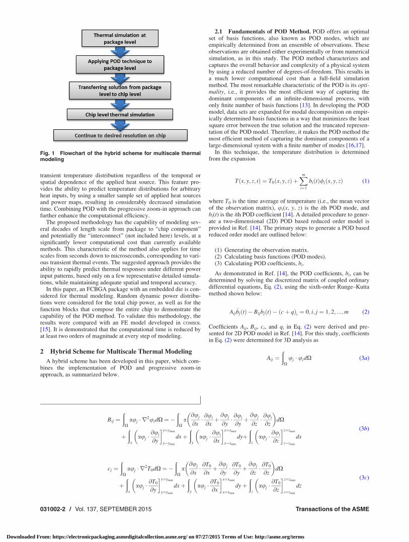
Fig. 1 Flowchart of the hybrid scheme for multiscale thermalmodeling
031002-2 / Vol. 137, SEPTEMBER 2015 Transactions of the ASME
Downloaded From: https://electronicpackaging.asmedigitalcollection.asme.org/ on 07/27/2015 Terms of Use: http://asme.org/terms

qj ¼ð
X
1
qcpuj � q000ðtÞdX (3d)
The last two terms on the right-hand side of Eqs. (3b) and (3c)are the boundary terms. If the boundary conditions are homogene-ous or insulation, these are eliminated and Bij and ci are simplifiedto
Bij ¼ �ð
Xa@uj
@x� @ui
@xþ@uj
@y� @ui
@yþ@uj
@z� @ui
@z
� �dX (4a)
cj ¼ �ð
Xa@uj
@x� @T0
@xþ@uj
@y� @T0
@yþ@uj
@z� @T0
@z
� �dX (4b)
(4) Generating the POD temperature field.
A sufficient number of POD modes and POD coefficients needto be calculated, which can then be used in Eq. (1) for the determi-nation of the temperature field anywhere in the domain and at anyinstant of time.
The number of retained POD modes is quite critical in captur-ing the physics of the problem. It is shown that an insufficientnumber of POD modes can cause significant phenomena not tobe detected [18]. On the contrary, taking too many POD modescan produce unexpected behavior or make the model unstable.The last POD modes are generally associated with low energyterms in the model and have rapid localized fluctuation through-out the domain. If too many modes are considered in the PODreconstruction, the accumulation of these rapid fluctuationsresults in an increase in the numerical error and can potentiallycause the solution to diverge [19,20]. The energy captured by theith basis function in the problem is relative to its correspondingeigenvalue, ki. Sorting these eigenvalues in a descending orderresults in an ordering of the corresponding POD modes [14].Therefore, the first POD mode captures the largest portion ofenergy relative to the other basis functions. To determine thetruncation degree of the POD method, the cumulative correlationenergy, Em, captured by the first m POD modes is defined byBizon et al. [21]
Em ¼
Xm
i¼1
ki
Xn
i¼1
ki
(5)
To be able to generate a reliable POD model, in the presentstudy, the number of POD modes is determined in such a way thatthe cumulative energy of the modes, calculated from Eq. (5), islarger than 99.9%.
2.2 Progressive Zoom-In Approach. The progressive zoom-in method integrates package and chip level analyses, acquiringthe advantages of each. Figure 1 shows a flowchart of theapproach used in this study for multiscale transient thermal mod-eling of a representative FCBGA package. The overall hybridapproach is outlined below:
(1) Thermal simulation at the package level: The first step is tomodel the entire structure, i.e., the package, including thesurrounding mold, underfill, solder bumps, and substrate.This simulation is performed in the commercial code COM-
SOL. It is important to note that at this level, the chip is mod-eled as a solid block with effective material and thermalproperties, without considering internal details.
(2) Applying POD technique to package level: Once the tem-perature distribution at package level is determined, a PODmodel is developed. The POD model provides the ability topredict dynamic temperature distribution for different
power maps and types of power sources, without develop-ing any further full-field FE models, which can significantlydecrease computational cost and potentially be used todefine a criterion for the optimal distribution of the currentdensity in the domain.
(3) Transferring the solution from package level to the chiplevel: Once the temperature distribution at the packagelevel is obtained, a combination of temperature and heatflux at the top and bottom walls of the chip is extracted andlinearly interpolated on a 2D grid with higher spatial reso-lution. These data were then applied as boundary conditionsfor the chip level simulation.
(4) Chip level thermal simulation: At this level, the chip is nolonger treated as a solid block. It is divided into subdomainscalled function blocks. Each block represents a specificcomponent with unique functionality on the chip and con-sists of three sublayers: (1) top Si layer, (2) middle devicelayer, and (3) interconnect/dielectric multilayer (see Fig. 2).Function blocks were simulated based on the assignedpower generation and calculated effective material/thermalproperties for each layer within that block. At this level ofthermal simulation, the spatial resolution is limited to thesublayers. Once the chip is divided into subdomains, thepower map needs to be determined at any instant of timefor each individual function block.
(5) Continue to the desired resolution on the chip: This methodcan be continued to multiple levels, such that the desiredspatial resolution is achieved. Only representative resultsfor two steps (package and chip level) are presented in thispaper.
3 Results and Discussion
Figure 2(a) shows the schematic of the simplified FCBGApackage used in this study for the package level modeling. Thismodel is for low power portable systems, where heat sinks andforced cooling are not employed due to the compact form factor.As described in Sec. 2, the first step is to model the package forwhich the material properties and dimensions are required. Table 1lists these for the die, solder bumps, underfill, mold, and substrate.These values were mainly provided by Mentor Graphics Corpora-tion, and the rest were chosen based on Ref. [22]. Reference [23]is used as a guideline for the dimensions of the FCBGA package.Underfill is a specially engineered epoxy that fills the areabetween the die and the carrier surrounding the solder bumps.Effective density and specific heat of the underfill layer are calcu-lated based on volume averaging. It is assumed that 60% of thesurface area between the die and substrate is covered with under-fill and 40% is solder bumps. The effective vertical (Kveff
) andhorizontal (Kheff
) thermal conductivity values are calculated basedon thermal resistor network formulation
Kheff¼ 1
8U
8tot
1
KU
þ 8S
8tot
1
KS
� � (6a)
Kveff¼ KU
AhU
Ah
þ KS
AhS
Ah
� �(6b)
where 8tot is the entire volume, 8U and 8S are volumes of underfilland solder bumps, respectively. Similarly, AhU and AhS are thecumulative horizontal cross-sectional areas of the underfill andsolder bumps. KU and KS are the thermal conductivities of theunderfill and solder bumps, respectively. Considering that thesolder bumps are made of conductive material and electricallyconnect the chip to the underlying substrate while underfill is aninsulating material, it is expected that the vertical effective ther-mal conductivity of the underfill layer will be significantly higherthan its horizontal value. The computed values are 20.2 and
Journal of Electronic Packaging SEPTEMBER 2015, Vol. 137 / 031002-3
Downloaded From: https://electronicpackaging.asmedigitalcollection.asme.org/ on 07/27/2015 Terms of Use: http://asme.org/terms

1.47 W/m�K, respectively. The package dimensions, also listed inTable 1, were provided by Mentor Graphics Corporation.
Natural convection boundary condition is imposed on the topsurface and vertical boundaries of the package with a heat transfercoefficient of h¼ 15 W/m2 K in the typical range for air cooling[24]. A constant temperature boundary condition is applied to thebottom surface. The initial temperature and the surrounding tem-perature were assumed to be equal to the room temperatureTamb¼ 300 K.
A detailed FE model is developed in COMSOL using a time stepof dt¼ 0.05 s. The convergence of the FE model is verified withrespect to the solver type, time step, and time integration method.The FE model of the package consists of 75,919 elements, ofwhich 343 are for the chip (die). This grid size is determined afterperforming mesh independence analysis. For the grid independ-ence study, the mesh resolution of the model is continuouslyrefined until there is less than 1% difference in the computed tem-peratures. This analysis indicated that the grid size of 75,919 ele-ments is sufficient. Total chip power is Q ¼ 3 sin 2ptþ 3 (W),which is applied for 1 s. The temperature rise in the simulation do-main is represented by DT (K) throughout the paper. Figure 3(a)
shows the spatial distribution of the temperature rise in theFCBGA package extracted from the FE model after 1 s. The tem-perature rise of the chip is plotted separately in Fig. 3(b). Table 2demonstrates the numerical solution parameters and specificationsused in package level FE model, POD technique, and chip levelFE model.
After obtaining the transient temperature field at the packagelevel, the POD model is developed using the algorithm demon-strated in Sec. 2.1. Twenty-six observations of the transient tem-perature solution were taken in the first 0.5 s using the packagelevel FE model. These observations correspond to the temperaturesolutions obtained at different time instants using total chip powerof Q ¼ 3 sin 2ptþ 3 (W). It is important to note that the observa-tions are generated only for this case, and results for any differentpower dissipation are calculated without any new observations. Infact, the POD solutions of these transient thermal scenarios are in-dependent of the initial observations. Essentially, for any linearsystem, once the solution to a sample case of chip total power isobtained, there is no need to generate new observations or performfull-field FE simulations. The ability of the POD method to pre-dict other cases based on a smaller sample set can significantly
Fig. 2 (a) Schematic of a simplified FCBGA for package level modeling and (b)zoomed-in schematic of the die layer used in chip level modeling
Table 1 Material properties and dimensions of the package
Thermal conductivity (W/m�K) Density (kg/m3) Specific heat capacity (J/kg�K) Dimension (mm3)
Die 98.4 2300 721 10� 10� 0.266Underfill 0.6 1820 236 10� 10� 0.1Solder bumps 50 8510 183 40% of the die surface areaEffective underfill 1.47 (horizontal)
20.24 (vertical)4496 214.8 60% of the die surface area
Mold 0.5 1820 236 37� 37� 1.9Substrate 0.7 1700 920 37� 37� 1.1
Fig. 3 Spatial distribution of temperature rise extracted from FE method after 1 s for (a)FCBGA package and (b) chip
031002-4 / Vol. 137, SEPTEMBER 2015 Transactions of the ASME
Downloaded From: https://electronicpackaging.asmedigitalcollection.asme.org/ on 07/27/2015 Terms of Use: http://asme.org/terms

decrease computational cost. After the observations have beengenerated, the POD basis functions (POD modes) are calculated.In order to build a reliable but fast reduced order model, only fourPOD modes are used in the present model. This is chosen suchthat the cumulative correlation energy, Em, Eq. (5), is greater than99.9%. The first two modes alone capture over 96% of the energy.The results will not have the desired accuracy if the number of ini-tial observations, n, is less than the minimum required PODmodes (four in the present case).
Since the POD modes are three-dimensional, for better visual-ization, 2D contours of the first four POD modes at heightz¼ 1.33 mm across the center of the die are illustrated in Fig. 4.This height is chosen because it has the highest temperature gradi-ent, due to material inhomogeneity and the application of powersource only to the die. The POD modes are normalized with thetotal sum of the modes for a more accurate comparison.
To have a realistic and accurate thermal simulation, a detaileddynamic power map of the embedded chip is required. However,one of the major challenges in microelectronics is the determina-tion of the dynamic power dissipation in the chip, since power val-ues and temperature distribution are coupled in an electrothermalloop. A randomly generated function is assumed for the dynamicchip power in this study to illustrate the application of the PODformulation. Figure 5(d) shows the randomly generated power dis-tribution for the chip for the first 1 s. The minimum and maximumallowed values for the power were chosen to be 3 W and 18 W,respectively. In essence, there are three changes in the nature ofthe previously used power source (Q ¼ 3 sin 2ptþ 3 (W)) and thecurrent random chip power:
(1) The first case is only applied for 0.5 s, whereas the secondcase used for POD approach models the entire 1 s.
(2) The magnitude of the maximum value for the second caseis 18 W versus 6 W for the initial FE simulation.
(3) The temporal behavior of the power has changed from awell-defined sinusoidal function to a randomly generatedstep function.
The benefit of using the POD model to predict the transientthermal profile for a different power source than the original oneis that no new observation or full-field simulation is required. ThePOD coefficients were calculated as functions of time using themethod of Galerkin projection [14].
Once the POD modes and the b-coefficients are calculated, thetransient temperature field can be determined using Eq. (1).Figure 6(a) displays the 3D spatial distribution of temperatureextracted from the POD model at 1 s. For higher precision, the do-main is sliced vertically along the XZ plane and four of these slicesare presented. The right-most slice is the A–A cross section acrossthe center of the die (Fig. 6(b)). To validate the results of the PODmodel, a full-field FE model with a time step of 0.05 s is developedin COMSOL using the same grid points and elements used in the PODmodel. The results are shown in Fig. 6(c). It can be inferred that thePOD model closely predicts the transient thermal behavior of thesystem, not only for the given time domain but also for projectedfuture time (>0.5 s) using just a few POD modes. The mean abso-lute error between the POD and FE model is 7.2% over the entirespace and time domain. Required computation time for the full-field FE simulation is 23.7 mins versus 40 s for the POD simula-tions. The first POD simulation run-time is 40 s, while additionalsimulations with different power sources take 15 s each. Thecomputations are performed on a workstation using an Intel(R)
Core (TM) i7 @ 2.20 GHz with 8 GB RAM.For a more comprehensive comparison between POD and FE
results, the time-dependent temperature rise at four differentpoints in the FCBGA package (center of the mold, die, underfill,and substrate) is considered (Fig. 7(a)). The maximum erroroccurs at the center of the die between t¼ 0.833 and t¼ 1 s. Asillustrated in Fig. 7(b), this is the time period when the maximum
Fig. 4 2D contour plots of the first four POD modes atz 5 1.33 mm from the bottom of the package; this plane crossesthe center of die
Fig. 5 Dynamic randomly generated power profile for functionblocks 1, 2, 10 (a–c) and randomly generated total chip power (d)
Table 2 Parameters of numerical solution
FE package level model POD package level model FE chip level model
Solver type Crank–Nicolson time integrationscheme and conjugate gradient iterative solver
Sixth-orderRunge–Kutta method
Crank–Nicolson time integration schemeand conjugate gradient iterative solver
Time step (s) 0.05 0.05 0.05Number of element 75,919 75,919 268,033Mesh independent Yes Yes YesSimulation time 23.7 mins 40 s (first run)
15 s (other runs)26.27 mins
Journal of Electronic Packaging SEPTEMBER 2015, Vol. 137 / 031002-5
Downloaded From: https://electronicpackaging.asmedigitalcollection.asme.org/ on 07/27/2015 Terms of Use: http://asme.org/terms

jump in the total chip power occurs. The dotted arrow in Fig. 7points to the time of this maximum jump in the temperature plot.
After obtaining the transient thermal solution at the packagelevel and with the POD model, the next step in the hybrid schemeis to transfer the solution to the chip with the higher spatial resolu-tion in the form of boundary conditions. Due to the transient
nature of this analysis, temperature on the top surface and heatflux on the bottom surface of the die are extracted at ten differenttime intervals between 0 and 1 s (every 0.1 s). The extracted dataare then applied as temporal boundary conditions for the chiplevel model. The four side walls of the die are assumed to be adia-batic considering the high aspect ratio of the die. The solution islinearly interpolated on a 2D grid with much higher spatial resolu-tion at this level (268,033 elements to model the chip at this levelversus 343 elements to model the chip at the package level).
At the chip level simulation, the die is no longer treated as asolid block. It is segmented into ten subdomains called functionblocks. In practical applications, each block represents a specificcomponent with unique functionality on the chip. In this study,the blocks were artificially created for illustration of the proposedmethodology [25]. As demonstrated in Fig. 2(b), each block hasthree layers: (1) top Si layer with the thickness of 0.249 mm, (2)middle layer which is a 5 lm-thick device layer, and (3) intercon-nect/dielectric multilayer at the bottom with the thickness of16.72 lm. The third layer consists of 21 sublayers including tenmetal layers.
Due to the high level of geometrical complexity, a combinationof directional volume and surface averaging methods was used todetermine the effective properties of the functional blocks. Table 3indicates the calculated material properties of the blocks at thechip level simulations. Density and specific heat are calculatedusing the volume averaging method. In-plane thermal conductiv-ity is determined based on the ratio of the volume of the intercon-nects to the total volume, due to the fact that the in-plane thermaltransport is governed mainly by the interconnects. On the otherhand, vias are the dominant paths of through-plane heat transfer ineach block. Therefore, for the vertical thermal conductivity, thevalues are calculated based on the ratio of the volume of the vias
Fig. 6 Spatial distribution of temperature rise at 1 s extracted from the POD model (a) and FEsimulation (c). The domain is sliced vertically along XZ plane. The right-most slice is the A–Across section (b).
Fig. 7 Comparison of temporal dependence of temperaturerise between FE (markers) and POD (solid lines) models at fourdifferent points (a) and the corresponding randomly generatedtotal chip power (b)
Table 3 Properties and dimensions of the function blocks for chip level simulation
Vertical thermalconductivity (W/m�K)
Horizontal thermalconductivity (W/m�K)
Density(kg/mm3)
Specific heatcapacity (J/kg�K)
Interconnect/dielectric layer
Block 1 0.48 3.53 1512.17 742.01Block 2 0.48 3.53 1512.16 742.01Block 3 0.49 3.56 1512.73 741.99Block 4 0.48 3.49 1511.44 742.05Block 5 0.49 3.66 1514.61 741.90Block 6 0.47 3.41 1509.90 742.12Block 7 0.49 3.58 1513.21 741.96Block 8 0.49 3.63 1514.20 741.91Block 9 0.48 3.49 1511.46 742.05Block 10 0.49 3.56 1512.82 741.98
Device layer 34 34 2320 678Si layer 130 130 2329 700
031002-6 / Vol. 137, SEPTEMBER 2015 Transactions of the ASME
Downloaded From: https://electronicpackaging.asmedigitalcollection.asme.org/ on 07/27/2015 Terms of Use: http://asme.org/terms

to the entire volume of each block. At this stage, the spatial reso-lution is limited to the sublayers of the blocks.
Once the chip is divided into subdomains, the dynamic powergrid needs to be assigned to individual function blocks. For thisstudy, the Joule heating produced in the third layer is neglectedand the only powered layer is the device layer. Using the samemethod as described earlier, ten random power sources with mini-mum and maximum values of 0 and 3 W were generated between0 and 1 s. The power sources for blocks 1, 2, and 10 are presentedin Figs. 5(a)–5(c) as representatives. The block power sources aregenerated in such way that their sum will equal the total chippower used for the package level simulation as shown in Fig. 5(d).
After allocating the power sources to the function blocks, an FEmodel is developed using the time step of dt¼ 0.05 s for the finalstep of the hybrid scheme. As mentioned, the model consists of268,033 elements. The computational time to run the transient sim-ulation for 1 s is 26.27 mins. Figure 8 displays the 2D spatial distri-bution of temperature rise extracted from the FE solution at varioustimes between 0 and 1 s at height z¼ 16.72 lm, which is the planebetween the device layer and interconnect/dielectric multilayer(plane between layers 2 and 3). Based on the one-dimensional sim-plified resistance-network model of the chip, it can be seen that themajority of heat generated at the device layer will be dissipatedthrough the top silicon layer and only about 5% of the heat is dissi-pated through the underlying interconnect/dielectric multilayer; i.e.,ðRthrough Si layer=Rthrough interconnet=dielectric layerÞ� 0.06.
4 Summary and Conclusion
In this study, a computationally efficient and accurate multi-scale reduced order transient thermal model is developed which
has the capability of modeling several decades of length and timescales at a considerably lower computational cost, while maintain-ing satisfactory accuracy. In particular, by using the proposedmodel, the computational time is reduced by at least two orders ofmagnitude at every step of zooming into the geometry. It is alsoshown that the hybrid scheme accurately predicts the transientthermal behavior of the system for not only the time domain con-sidered for the initial observations, but also for time outside of thespecified initial time domain. The mean absolute error betweenthe proposed and FE model is 7.2% over the entire space and timedomain.
A distinct benefit of the proposed method is that, for any linearsystem, the POD solution is independent of the transient powerprofile. In other words, once the solution to a sample power inputis obtained, there is no need to generate new observations or full-field FE simulations. This important feature can drasticallydecrease computational cost for parametric numerical simulations,making POD a fast and robust method for reduced order model oftransient heat conduction in microelectronic devices. An addi-tional unique characteristic of this model is that the initial obser-vations can be obtained experimentally, which creates the abilityof modeling a potentially complex system without generating anynumerical model.
The hybrid scheme proposed in this study is not limited to thetwo levels considered in the present study and can potentiallyextended from package to “interconnect level.” One of thestrengths of this method is that the algorithm can be scaled to mul-tiple levels and can be used to simulate more detailed structureson the chip, while taking advantage of the capabilities of PODmethod to avoid any further full-field simulation. In essence, with-out losing the desired resolution, the hybrid scheme proposes anew approach to further decrease the computational cost by ordersof magnitude.
The integration of the proposed method into the commerciallyavailable software packages can create a powerful tool for bothacademic and industry applications. It will address the lack ofphysical models for multiscale thermal problems, relating poten-tial performance variation to critical layout parameters. Anotherpossible application of this method would be in the IC designindustry. A POD model can be developed for a specific chip struc-ture using output signals of the embedded temperature sensors onthe chip as the original observations. By incorporating this modelinto a closed-loop on-chip control system, the possible locationsof hot-spots can then be predicted and potentially avoided.
Acknowledgment
The research is partially funded by the Semiconductor ResearchCorporation (SRC) under Task 1883.001 and Design-to-Silicondivision of Mentor Graphics Corporation.
Nomenclature
A ¼ cross-sectional area (m2)Aij ¼ coefficient in Eq. (2)bi ¼ ith POD coefficient (K)
Bij ¼ coefficient in Eq. (2)ci ¼ coefficient in Eq. (2)dt ¼ time step (s)
Em ¼ cumulative correlation energyh ¼ heat transfer coefficient (W/m2 K)K ¼ thermal conductivity (W/m�K)m ¼ number of POD modes usedn ¼ number of observationsQ ¼ total chip power (W)qi ¼ coefficient in Eq. (2)t ¼ time (s)
T ¼ temperature (K)T0 ¼ time averaged temperature (K)
z ¼ height (mm)
Fig. 8 Transient temperature distribution at the interface ofdevice and interconnect/dielectric layers: t 5 0, 0.2, 0.4, 0.6,0.85, and 0.95 s
Journal of Electronic Packaging SEPTEMBER 2015, Vol. 137 / 031002-7
Downloaded From: https://electronicpackaging.asmedigitalcollection.asme.org/ on 07/27/2015 Terms of Use: http://asme.org/terms

Greek Symbols
ki ¼ ith eigenvalueui ¼ ith POD mode
Subscripts
amb ¼ room/ ambienthS ¼ solder bumps (horizontal)hU ¼ underfill (horizontal)
h_eff ¼ effective horizontal valueS ¼ solder bumps
tot ¼ totalU ¼ underfill
v_eff ¼ effective vertical value
References[1] Gurrum, S. P., Joshi, Y. K., King, W. P., Ramakrishna, K., and Gall, M., 2008,
“A Compact Approach to On-Chip Interconnect Heat Conduction ModelingUsing the Finite Element Method,” ASME J. Electron. Packag., 130(3),p. 031001.
[2] Joshi, Y., 2012, “Reduced Order Thermal Models of Multiscale Microsystems,”ASME J. Heat Transfer, 134(3), p. 031008.
[3] Christiaens, F., Vandevelde, B., Beyne, E., Mertens, R., and Berghmans, J.,1998, “A Generic Methodology for Deriving Compact Dynamic Thermal Mod-els, Applied to the PSGA Package,” IEEE Trans. Compon., Packag., Manuf.Technol., Part A, 21(4), pp. 565–576.
[4] Lasance, C., Vinke, H., Rosten, H., and Weiner, K. L., 1995, “A NovelApproach for the Thermal Characterization of Electronic Parts,” EleventhAnnual IEEE Semiconductor Thermal Measurement and Management Sympo-sium (SEMI-THERM XI), San Jose, CA, Feb. 7–9.
[5] Gerstenmaier, Y., and Wachutka, G., 2002, “Rigorous Model and Network forTransient Thermal Problems,” Microelectron. J., 33(9), pp. 719–725.
[6] Krueger, W., and Bar-Cohen, A., 1992, “Thermal Characterization of a PLCC-Expanded Rjc Methodology,” IEEE Trans. Compon., Hybrids, Manuf. Technol.,15(5), pp. 691–698.
[7] Celo, D., Xiao Ming, G., Gunupudi, P. K., Khazaka, R., Walkey, D. J., Smy, T.,and Nakhla, M. S., 2005, “Hierarchical Thermal Analysis of Large IC Mod-ules,” IEEE Trans. Compon. Packag. Technol., 28(2), pp. 207–217.
[8] Hua, Y., and Yu, Z., 1989, “Generalized Pencil-of-Function Method forExtracting Poles of an EM System From Its Transient Response,” IEEE Trans.Antennas Propag., 37(2), pp. 229–234.
[9] Hua, Y., and Yu, Z., 1991, “On SVD for Estimating Generalized Eigenvalues ofSingular Matrix Pencil in Noise,” IEEE Trans. Signal Process., 39(4), pp. 892–900.
[10] Zao, L., Tan, S. X. D., Hai, W., Quintanilla, R., and Gupta, A., 2011, “CompactThermal Modeling for Package Design With Practical Power Maps,” InternationalGreen Computing Conference and Workshops (IGCC), Orlando, FL, July 25–28.
[11] Duo, L., Tan, S. X. D., Pacheco, E. H., and Tirumala, M., 2009, “Architecture-Level Thermal Characterization for Multicore Microprocessors,” IEEE Trans.VLSI Syst., 17(10), pp. 1495–1507.
[12] Lumley, J. L., 1967, “The Structure of Inhomogeneous Turbulent Flows,”Atmospheric Turbulence and Radio Wave Propagation, Nauka, Moscow,pp. 166–178.
[13] Holmes, P., Lumley, J. L., and Berkooz, G., 1998, Turbulence, CoherentStructures, Dynamical Systems and Symmetry, Cambridge University Press,Cambridge, UK.
[14] Barabadi, B., Joshi, Y., and Kumar, S., 2011, “Prediction of Transient ThermalBehavior of Planar Interconnect Architecture Using Proper Orthogonal Decom-position Method,” ASME Paper No. IPACK2011-52133.
[15] COMSOL, 2011, “COMSOL Version 4.2,” Comsol Multiphysics, Inc., Burlington,MA, http://www.comsol.com
[16] Chatterjee, A., 2000, “An Introduction to the Proper Orthogonal Decom-position,” Curr. Sci., 78(7), pp. 808–817.
[17] Berkooz, G., Holmes, P., and Lumley, J., 1996, Turbulence, Coherent Struc-tures, Dynamical Systems and Symmetry (Cambridge Monographs on Mechan-ics), Cambridge University Press, Cambridge, UK, pp. 1200–1208.
[18] Graham, M. D., and Kevrekidis, I. G., 1996, “Alternative Approaches to theKarhunen–Loeve Decomposition for Model Reduction and Data Analysis,”Comput. Chem. Eng., 20(5), pp. 495–506.
[19] Rowley, C. W., Colonius, T., and Murray, R. M., 2001, “Dynamical Models forControl of Cavity Oscillations,” AIAA Paper No. 2001-2126.
[20] Samadiani, E., Joshi, Y., Hamann, H., Iyengar, M. K., Kamalsy, S., and Lacey,J., 2012, “Reduced Order Thermal Modeling of Data Centers Via DistributedSensor Data,” ASME J. Heat Transfer, 134(4), p. 041401.
[21] Bizon, K., Continillo, G., Russo, L., and Smula, J., 2008, “On Pod ReducedModels of Tubular Reactor With Periodic Regimes,” Comput. Chem. Eng.,32(6), pp. 1305–1315.
[22] Incropera, F. P., Bergman, T. L., Lavine, A. S., and Dewitt, D. P., 2011, Funda-mentals of Heat and Mass Transfer, Wiley, Hoboken, NJ.
[23] Chang, K. C., Li, Y., Lin, C. Y., and Lii, M. J., 2004, “Design Guidance for theMechanical Reliability of Low-K Flip Chip BGA Package 1,” 37th Interna-tional Microelectronics and Packaging Society (IMAPS) Topical Workshop andExhibition on Flip Chip Technology, Long Beach, CA, Nov. 14–18, pp. 21–24.
[24] Tang, L., and Joshi, Y. K., 2005, “A Multi-Grid Based Multi-Scale ThermalAnalysis Approach for Combined Mixed Convection, Conduction, and Radia-tion Due to Discrete Heating,” ASME J. Heat Transfer, 127(1), pp. 18–26.
[25] Barabadi, B., Kumar, S., Sukharev, V., and Joshi, Y. K., 2012, “Multi-ScaleTransient Thermal Analysis of Microelectronics,” ASME Paper No.IMECE2012-89864.
031002-8 / Vol. 137, SEPTEMBER 2015 Transactions of the ASME
Downloaded From: https://electronicpackaging.asmedigitalcollection.asme.org/ on 07/27/2015 Terms of Use: http://asme.org/terms