automatic scoring system - intel.com · the system stores audio materi al onto a secure digital...
TRANSCRIPT
Automatic Scoring System
Third Prize
Automatic Scoring System
Institution: Huazhong University of Science & Technology
Participants: Ya-bei Yang, Zun Li, and Yao Zhao
Instructor: Xiao Kan
Design IntroductionHistory records what happened in the past. Do you remember the 23rd Olympic Games in Los Angeles? Xu Haifeng, the Chinese athlete, won China’s first gold medal for shooting. Do you remember the 1992 Olympic Games in Barcelona? Zhang Shan, a female Chinese athlete, outperformed all male athletes and became the only female champion in the history of skeet shooting. Do you remember the 1996 Olympic Games in Atlanta and the 2000 Olympic Games in Sydney? The shooting athlete Yang Ling twice won the 10 meter running target championship and became the only repeat winner until today. Do you remember the 2004 Olympic Games in Athens? In an unprecedented sweep, the Chinese athletes Du Li, Wang Yifu, Zhu Qi’nan, and Jia Zhanbo won 4 gold, 2 silver, and 3 bronze medals, and the five-starred red flag flew time and time again on the Olympic field. Over the past 50 years, Chinese shooting athletes have won 14 Olympic gold medals, 113 world championships, and broken records 117 times. In short, shooting has become a competitive Chinese sport. We strongly believe that Chinese athletes will make additional progress in the upcoming 2008 Olympic Games in Beijing.
While taking pride in Chinese athletes’ achievements, have you paid attention to the software and hardware used for Chinese shooting? We investigated which automatic targets and electronic scoring systems Chinese athletes used, and found that most are not made in China: they are imported. For example, we visited the Hubei Shooting Management Center to investigate their setup. The Hubei shooting ground only has two or three sets of devices, which are imported from Germany. Each set costs about 100 thousand RMB. Therefore, the athletes do not use the devices for daily training: they only use them for official situations. Even the automatic targets and electronic scoring systems that the athletes will use in the 2008 Olympic Games in Beijing are imported by BOCOG from Swizerland (from Sius). This research does not even consider the devices used for our troops, police, and training grounds!
We need a cheap, practical automated target and electronic scoring system. If we can develop this product, it will significantly improve the shooting skill of China’s athletes and modernize China’s shooting devices.
123

Nios II Embedded Processor Design Contest—Outstanding Designs 2006
Design ObjectiveOur goal was to develop a small, intelligent automatic scoring system for training and shooting competitions. We placed a high-resolution camera in front of the target (at the bottom) that takes a real-time image of the target plane. We then use an FPGA to analyze the shot, calculating the bullet’s location and determining it’s position on the target. The bullet hole is tracked for each shot, helping the human replacing the target to avoid danger.
Related Research and Current SituationThere are four basic types of automated scoring systems:
■ Double-layer electrode short-circuit sampling—This method has a very low reporting rate and does not work for round or short headed pistols. Additionally, it does not work for tracer bullets and has a low reporting rate for ordinary long bullets.
■ Laser diode array—In this method, a laser diode and the receiving tube are placed in a line. The bullet blocks the diode-emitted laser when the bullet passes through the diode, which generates a pulse at the laser receiving circuit. The background circuit can determine the circular number based on this signal. The system can report the target’s circular number without target paper, but it is difficult to improve the reporting accuracy because small-diameter laser diodes are not available.
■ Sound positioning—Today’s media frequently shows the sound positioning scoring system. This method uses four sound sensors on the four corners of the target. It uses the noise the bullet makes when it passes through the target to determine the bullet’s position. Because it uses a lot of technology, the sound sensor is very expensive. Additionally, the system has comparatively high on the target plane requirements, because the target paper must be made of special material so that it generates enough sound. These restrictions will prevent wide use of the system.
■ Image processing—The system determines the bullet hole’s position by analyzing the bullet’s image on the target plane. Theoretically, this method is very accurate, even better than sound positioning. With a camera that has millions of pixels, the system can meet competition demands at a low price. Provided the costs can be lowered enough, this system can be used in a wide range of applications, can help improve Chinese athlete’s shooting ability, and break the automatic scoring system monopoly.
Today, companies and institutes are researching video-processing-based automated scoring systems. However, most of them use a PC to deal with the video. Compared to an embedded system, a PC has poor stability, adaptability, and size, and is not suitable for outdoor use or the special training needs of army and police systems.
Design ArchitectureThis section describes the design architecture and system function.
System FunctionLooking at the shooting field structure, the system is composed of a target-side image processing front end and an athlete-side human-machine interaction back end. The system integrates image processing, dual-machine communication, and human-machine interaction functions. See Figure 1.
124

Automatic Scoring System
Figure 1. General System Functions
Image Processing FunctionThe design has the following image processing functions:
■ Bullet hole identification—The FPGA controls the camera to collect the image, saves the pixel array into the SDRAM on the Development and Education (DE2) board for buffering, and then reads the data to apply a template-matching algorithm and identify the bullet hole. The function converts the coordinates to determine the bullet hole’s coordinates and circular number.
■ Bullet hole tracking (automatic adjustment of the target paper)—We used a closed-loop feedback control mechanism based on the bullet hole identification function. The system can effectively track the bullet hole and control the paper feeding mechanism to adjust the target paper automatically. This setup helps the person replacing the target avoid danger and ensures security.
Communication FunctionThe design has the following communication functions:
■ RS-485 transmission—To meet the transmission distance demand on the front or back end while ensuring correct data transmission, the system uses the RS-485 bus to provide duplex communication between the image processing front end and human-machine interaction back end.
■ Wireless transmission—To increase the system’s flexibility, we use software radio technology to wirelessly transmit data between the front and back end.
Function
LCDDisplays the
Scores
PrintedScore Record
Storage onSD Card
Audio Broadcast
RS-485Transmission
WirelessTransmission
DE2 Board DE2 Board
RS485 bus
Software radio
Bullet HoleIdentification
Bullet HoleTracking
ImageProcessing
Machine VisualSource of Light
Image Tracking
AutomaticControl
Human-MachineInteraction Back End
Image ProcessingFront End
Related Technology
AlteraCyclone II
FPGA
AlteraCyclone II
FPGA
Nios IICPU
Nios IICPU
Voice ShootingReport
TimingService
125

Nios II Embedded Processor Design Contest—Outstanding Designs 2006
Data Exchange FunctionThe system has the following data exchange functions:
■ LCD display—The display is an important tool for providing information. This system uses a 640 x 480 LCD module to display the real-time competition scores, letting athletes easily access competition information.
■ Printer—Printing is a simple, effective way to store information and is vital rating proof in shooting competitions. Therefore, the micro-printer module is an integral part of our system. We use a TPUP-T16 series dot matrix printer to record the athletes’ scores and thereby calculate the total scores.
■ Voice reporting—To inform the audience of the competition progress, the system has an audio reporting function. The system stores audio material onto a secure digital (SD) card and delivers the data to a 24-bit audio codec when the card is read, resulting in voice broadcasting.
■ Timing service—The International Shooting Sport Federation imposes stringent shooting time requirements. We added a system clock service to the human-machine interaction back end to provide an electronic clock and use the DE2 development board’s four built-in keys to implement the time setup.
System ArchitectureThe system is composed of a target-side image processing front end and the athlete-side human-machine interaction back end. The front-end DE2 board collects and processes the image and communicates with the back-end board. The back-end DE2 board communicates with the front-end board and provides the human-machine interaction environment. Figure 2 shows the architecture.
Figure 2. Automatic Scoring System Architecture
We used two Nios® II processors for the image processing front end and human-machine interaction back end. The Nios II processors control data collection and processing, provide communication, and establish an interactive environment. The RS-485 connection and a radio allow the front and back end to communicate, making the system flexible and adaptable.
Nios II Architecture: Image Processing Front EndThe Nios II system in the image processing front end controls the image sensor, data collection and processing, paper feeding mechanism, and data transmission. Figure 3 shows the detailed architecture.
LED
Printer
Nios IINios II640 x 480
LCD
16 x 2 LCDDisplay Clock
Voice ShootingBroadcast
InputDevice
RS-232
DigitalDecoding
AnalogReceiving &
Demodulation
ConvertRS-232 toRS-485
Human-Machine InteractionBack-End Nios II System
Image-Processing Front-EndNios II System
ConvertRS-232 toRS-485
RS-232 Image Sensor Control
& Image Processing
CMOSImageSensor
ElectricMachine
Control I/O
ElectricMachine
D/A ConversionHigh-Frequency
PowerAmplifier
DigitalIntermediateFrequency
CommunicationCables
DE2 BoardDE2 Board
126

Automatic Scoring System
Figure 3. Nios II Architecture of the Image Processing Front End
The FPGA collects an image with a CMOS camera, saves the pixel array into the DE2 board’s SDRAM for buffering, and reads the data to apply a template-matching algorithm and identify the bullet hole. The Nios II embedded processor converts the coordinates and calculates the bullet hole’s coordinates and circular number. It uses a UART peripheral to switch the RS-485 bus interface, and follows the RS-485 bus specification to make the transmission distance meet the system demand. The self-defined pulse width modulation (PWM) controller peripheral controls the direct current machine that automatically adjusts the target paper. The programmable I/O (PIO) inferface controls the wireless transmission module directly. Because the SDRAM contains the image collecting units, the system self-defines the peripherals (using an interface to user logic) to implement SRAM controller and run the programs in SRAM.
Nios II Architecture: Human-Machine Interaction Back EndThe Nios II system in the human-machine interaction back end receives data sent from the front-end system, displays and prints the results in real time, and provides a human-machine interaction interface, clock service, etc. See Figure 4.
JTAGDebug Module
Nios II Fast Processor
Core
Interfaceto User Logic
EPCSController
SRAMMemory
Tri-State BridgeOff-ChipMemory
AvalonSwitchFabric
Timer
PIO
PIO
PIO
RS-485
Clock Reset
Data
Instr.
Paper FeedingMechanism
Press Key
WirelessTransmission Module
UART
PWM
Image ProcessingUnit
CMOS Camera
System ID
DataAddress
WRRDCS.
127

Nios II Embedded Processor Design Contest—Outstanding Designs 2006
Figure 4. Nios II Architecture of the Human-Machine Interaction Back End
We take advantage of the peripherals provided with the Nios II processor: two UART peripherals implement the RS-485 switch and printer control. We use multiple PIO peripherals to build the connection between the 640 x 480 LCD controller and the wireless receiving module. A system timer generates a clock and provides a timing service for the peripheral LCD 16207 and the seven-segment numeric display. Switches and keys provide human-machine interaction.
Function DescriptionThis section describes the various modules in our design.
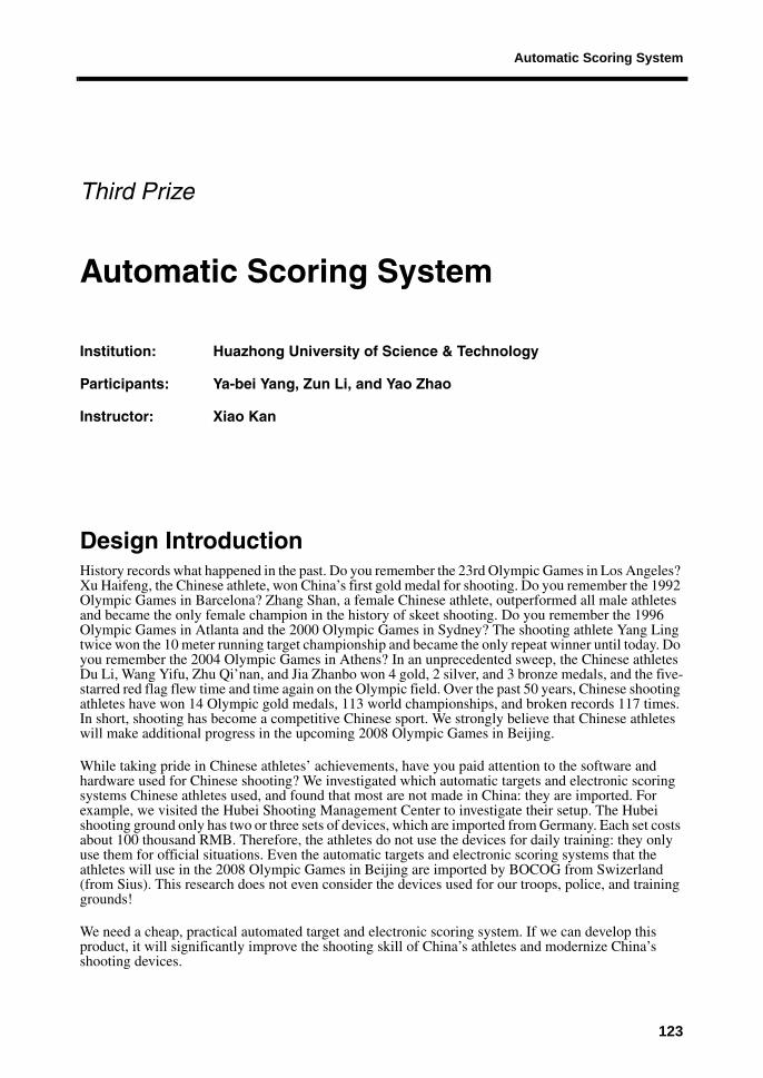
Image Processing ModuleImage processing module is the core of the system; it identifies and positions the target and converts the coordinates. In the module design, we applied an image processing algorithm in hardware and used software to convert the matched coordinates and track the target. Figure 5 shows the image processing hardware circuit.
JTAGDebug Module
Nios II Processor
Core
Interfaceto User Logic
EPCSController
SDRAMMemory SDRAM
Controller
AvalonSwitchFabric
UART1
Timer
User Logic
LCD DisplayDriver
PIO
PIO
PIO
RS-485
Clock Reset
Data
Instr.
LCD DisplayModule
WirelessReceiving Module
Switch
UART2
PIO
Printer
Clock
Press Key
Seven-SegmentDisplay
LCD 16207
128
Automatic Scoring System
Figure 5. Image Processing Hardware Circuit
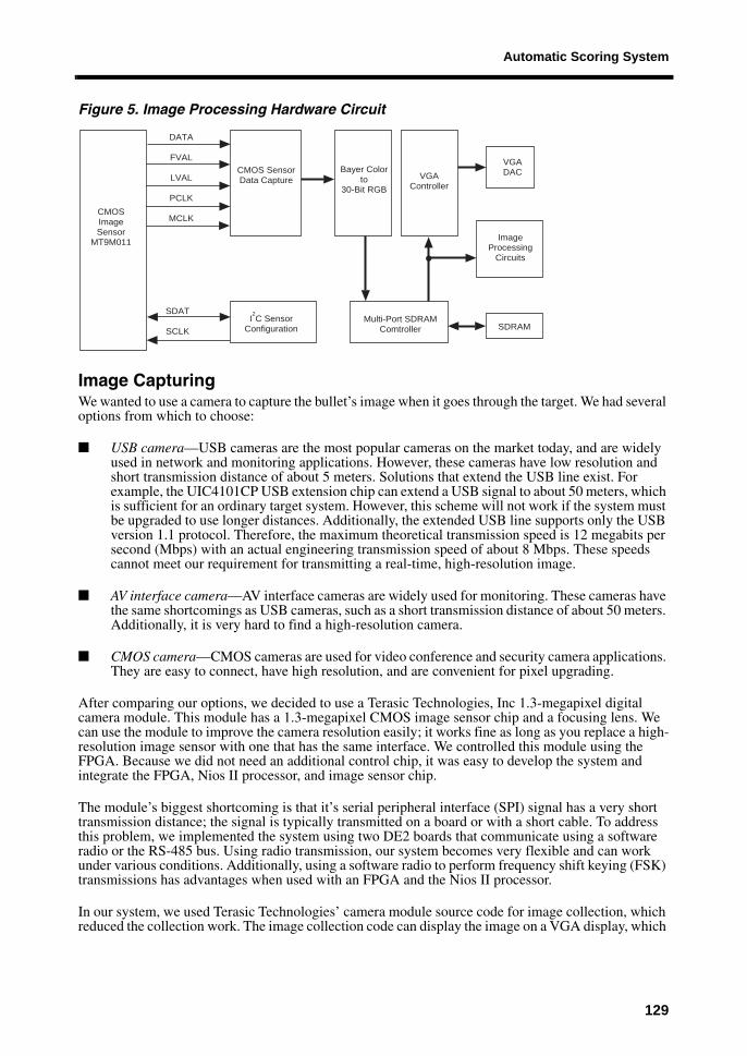
Image CapturingWe wanted to use a camera to capture the bullet’s image when it goes through the target. We had several options from which to choose:
■ USB camera—USB cameras are the most popular cameras on the market today, and are widely used in network and monitoring applications. However, these cameras have low resolution and short transmission distance of about 5 meters. Solutions that extend the USB line exist. For example, the UIC4101CP USB extension chip can extend a USB signal to about 50 meters, which is sufficient for an ordinary target system. However, this scheme will not work if the system must be upgraded to use longer distances. Additionally, the extended USB line supports only the USB version 1.1 protocol. Therefore, the maximum theoretical transmission speed is 12 megabits per second (Mbps) with an actual engineering transmission speed of about 8 Mbps. These speeds cannot meet our requirement for transmitting a real-time, high-resolution image.
■ AV interface camera—AV interface cameras are widely used for monitoring. These cameras have the same shortcomings as USB cameras, such as a short transmission distance of about 50 meters. Additionally, it is very hard to find a high-resolution camera.
■ CMOS camera—CMOS cameras are used for video conference and security camera applications. They are easy to connect, have high resolution, and are convenient for pixel upgrading.
After comparing our options, we decided to use a Terasic Technologies, Inc 1.3-megapixel digital camera module. This module has a 1.3-megapixel CMOS image sensor chip and a focusing lens. We can use the module to improve the camera resolution easily; it works fine as long as you replace a high-resolution image sensor with one that has the same interface. We controlled this module using the FPGA. Because we did not need an additional control chip, it was easy to develop the system and integrate the FPGA, Nios II processor, and image sensor chip.
The module’s biggest shortcoming is that it’s serial peripheral interface (SPI) signal has a very short transmission distance; the signal is typically transmitted on a board or with a short cable. To address this problem, we implemented the system using two DE2 boards that communicate using a software radio or the RS-485 bus. Using radio transmission, our system becomes very flexible and can work under various conditions. Additionally, using a software radio to perform frequency shift keying (FSK) transmissions has advantages when used with an FPGA and the Nios II processor.
In our system, we used Terasic Technologies’ camera module source code for image collection, which reduced the collection work. The image collection code can display the image on a VGA display, which
CMOSImageSensor
MT9M011
CMOS SensorData Capture
I2C Sensor
Configuration
Bayer Colorto
30-Bit RGBVGA
Controller
Multi-Port SDRAMComtroller
VGADAC
ImageProcessing
Circuits
SDRAM
DATA
FVAL
LVAL
PCLK
MCLK
SDAT
SCLK
129

Nios II Embedded Processor Design Contest—Outstanding Designs 2006
helped us build an image-processing platform. We added our image processing code to the collection code. The image collection operates as follows:
1. Configure the image sensor using the I2C bus.
2. Read the collected image dot matrix according to the timing attributes of the image sensor.
3. Use algorithms to convert the dot matrix Bayer color space to the RGB color space.
4. Save the dot matrix data to SDRAM.
5. The VGA display code reads the data from the SDRAM. Because the SDRAM controller has a dual-port control, our image-processing code can read data from the SDRAM.
Image ProcessingThis section describes the image processing algorithms and hardware circuit we used in our design.
Image Processing Algorithm Selection and AnalysisDue to circuit power noise and the image sensor chip’s limitations, the analog-to-digital (A/D) sensor conversion result has a lot of noise. Even if the sensor converts the same image, there is a difference in the image array data produced by different frame numbers generated at a different time. Comparing two images to judge the target position involves image fuzzy processing and other complicated algorithms.
To solve this problem, we use an innovative template matching algorithm. The algorithm has a two-dimensional (2D) filtering effect, which eliminates traditional median filtering and image smoothing and completely removes noise, which accelerates the speed. We were confident that the algorithm could achieve the target check. Figure 6 shows the template matching algorithm.
Figure 6. Template Matching Algorithm
The template matching algorithm performs target searching and positioning. The template matching step compares a specific area in the original image to a known template (in this design it is the target image) of the same size. If the compared image domain value is within a specified range, the images match. We start with the upper left point of the template and image and compare an area of the template to the same size area in the original image. Then, we move to the next pixel and perform the same operation. After all areas are compared, the area that meets our specified domain value is the target that we want.
We use the difference of the pixel domain values to measure the difference of the target template and target plane. The suggested the template size is m x n (i.e., width by height) and the image size is width x height. The coordinates of a template point are x0, y0, the point’s grey level is U (x0, y0), the
ImageHeight
Image Partto be Matched
Image Width
M
Template
130

Automatic Scoring System
coordinates of the coincident point in the image is X0 - x0, Y0 - y0, and the grey level is V (X0 - x0, Y0 - y0), yielding a matched result of:
During matching, the point that meets our specified domain value is the result. Template matching requires considerable operations. The m x n subtraction and m x n - 1 addition must be made for each match, and the whole image requires (width - m + 1) x (height - n + 1) iterations. Additionally, the software processing template matching algorithm performs circular operations, which requires a lot of calculations. The operation volume increases rapidly as the template is enlarged. However, if we perform the process in hardware using a parallel, pipelined architecture, we can increase the processing speed remarkably. With this implementation, enlarging the template does not affect the processing speed, it simply affects the circuit size.
Validating the Image Processing AlgorithmBefore implementing the video processing in hardware, we used software to validate the algorithm. We used software because it is comparatively more mature and is more flexible for computer-based design tuning. Additionally, software provides a variety of image processing functions that we can call directly and conveniently. In contrast, there are only a few methods available for hardware tuning. We used the MATLAB software to validate the algorithm, which proved that our concept was the same as the implementation. Then, we converted the software algorithm into hardware to perform the image processing.
During the algorithm validation, we used the DE2_Control_Panel software that came with the DE2 board to read image data from SDRAM. The Image_Converter_v1.1 software translates the RGB format data from the camera into bitmap format. The MATLAB image processing function processes the picture file in bitmap format. We used the following key MATLAB functions:
Imagedata=imread('target. bmp');Twovalue=im2bw(Imagedata);Imshow(Twovalue);
Figure 7 shows the image from the camera and Figure 8 shows the image after it is converted to binary. The target position is obvious in the binary file. However, if a bright light is added in front of the target plane, the whole target plane has light reflection. In this case, the image sensor’s converted A/D result is saturated and influences the target judgment (the light directly operates the exposure registry in the image sensor chip). Controlling the camera’s exposure time reduces the sunlight input to the camera, which decreases the camera’s value after A/D conversion and makes the target identifiable. This solution solves the problem of a bright light on the target plane, making the system more adaptable and validating the advantages of using the image sensor chip directly. After we chose the right domain value, the target position in the image can be identified.
U x0 y0,( ) V X0 x0– Y0 y0–,( )–
x0 0=
m 1–
∑y0 0=
n 1–
∑
131

Nios II Embedded Processor Design Contest—Outstanding Designs 2006
Figure 7. Target Plane Image
Figure 8. Target Plane Image after Binarization
Image Processing Algorithm Hardware Circuit and ConceptsThe system’s image processing module has an innovative hardware template matching algorithm. We got this concept from the software template matching algorithm and the hardware median filtering algorithm. It has the speed and agility of hardware processing, which is superior to the software template matching algorithm and the hardware median filtering algorithm regardless of the computing volume or complexity.
We used the shift register from the library of parameterized modules (LPM) in the Quartus® II software, simplifying the system design and optimizing the code. The shift register length is the length of the horizontal line of the image. We use 640 horizontal pixels in the design.
In the design we used a 4 x 4 template, i.e., 16 processing units (PEs), each of which is a domain value computing circuit synchronized with the clock. The 4-level pipeline structure provides parallel processing. When a synchronized clock signal arrives, the template processing structure generates 16 domain values that are sent to the addition circuit to compute the template’s total domain value. We compare the computed result to the preset domain value. If it is smaller than the preset value, the template is assumed to match the target. An external interrupt is sent to the Nios II CPU, allowing the CPU to read the coordinates that matched the target. The remaining work is performed in software. Figure 9 shows the hardware image processing algorithm.
132

Automatic Scoring System
Figure 9. Hardware Image Processing Algorithm Structure
Image Processing Light Source DesignThe light source design plays a key role in the machine’s vision. In fact, the light source determines whether the machine vision is successful. Therefore, we fully consider the light source in the system design. To reduce costs, we use a general fluorescent lamp instead of a professional light source. To solve the fluorescent lamp’s light quality problems, we added a baffle plate behind the target plane to capture the bullets and diffuse the light. The baffle makes the light through the target even and bright, which improves the system’s target identification and enhances it’s adaptability to the external light. This design enhances the system’s adaptability, and light from the incandescent lamp in front of the target plane does not affect the target identification accuracy.
Changing the Coordinate SpaceThe camera must be put on the upper left, upper right, or below the target plane. In these positions, it leans at an angle, which transmutes the collected image to a certain degree. In our design, we place the camera below the target plane with an iron board to protect it. Figure 10 shows the camera position.
SDRAM
Image LineShift Register
Register 1 Register 2 Register 3 Register 4
Addition CircuitDomain Value
Computing
Compare the CircuitDomain Value
Judgement
PE PE PE PE
Meet the Requirements& Output the Result
Nios II CPU
PE
PE Circuit Structure
CLK
iData
rst_n
oData_bak
result
PE PE PE PE
PE PE PE PE
PE PE PE PE
133

Nios II Embedded Processor Design Contest—Outstanding Designs 2006
Figure 10. Spatial Position of the Camera Relative to the Target Plane
As shown in Figure 10, Hup > Hdown, that is, as a point moves further from the camera, the line collected by the camera becomes longer. Because the camera’s horizontal pixel point is fixed, as two pixels move further away from the camera, the distance between them becomes longer. From a vertical perspective, the two pixel’s image distances collected by the camera are different too. The camera we used has a short focus, so we ignored the focus effect and considered the camera to be a point. This point forms an angle with the upper and lower border, which is divided into the same angles by the camera’s vertical resolution. The target plane’s real distances for each corresponding angle are different. The target plane’s left and right camera also form an angle, which is affected by the vertical direction. Therefore, the problem is one of three-dimensional (3D) coordinate changes. To obtain the actual score, we need to find the actual shooting position. The design finds the actual distance between the target and the center of the target plane, and then computes the corresponding score according to the target plane standard.
Figure 11 shows the relative spatial positions of the target and target plane.
Figure 11. Relative Spatial Position of the Target and the Target Plane
We need to compute the actual target coordinates (shown as a black circle in Figure 11). The horizontal resolution is PixelH and the vertical resolution is PixelV. The coordinates collected during the target’s
Hup
Hv
Hdown
Lh
Hv
Hdown
Lh
134

Automatic Scoring System
image identification are Xtemp, Ytemp. To obtain the actual coordinates and the score, we perform the following computations.
The actual vertical distance from the target to the lower border is:
The actual vertical distance from the target to the center of the target plane is:
The actual distance from the target to the vertical central line is:
The actual distance from the target to the center of the target plane is:
We can compute the actual score with this data. The design uses the target plane for a 25-meter air rifle, in which the actual size of the central circle is 10 mm (score: 2) and other circles are 8 mm (score: 1). The actual score can be computed with the real distance between the target and the center of the target plane. If Lcenter < 5, the actual score is:
If Lcenter >= 5, the actual score is:
Software (Nios II) and Hardware (FPGA) CooperationThe hardware (FPGA) processes the image to obtain the relative position of the target. When the hardware identifies the target, it sends an interrupt signal to the Nios II CPU. The hardware processing result is read after the CPU enters the interrupt service program generated by the image processing hardware unit, i.e., the identified X, Y coordinates. The software transforms the X, Y coordinates into actual coordinates and continues the transfer work. With this method, the system uses both hardware speed and software agility.
Image TrackingAfter the target position is identified, the system adds automated target tracking to adjust and replace the target sheet strip automatically. This process avoids confusing the targets and improves system security by preventing manual interference of the target sheet. If we used a preset distance it would waste the paper strip. Instead, we used a closed-loop control design concept to move the paper strip to the shortest position from which the bullet hole cannot be seen. Figure 12 shows the target tracking algorithm’s software/hardware cooperation.
Lv Lh TtempPixelV------------------⎝ ⎠
⎛ ⎞tan×=
Lvcenter Hv2
------- Lv–=
Lhcenter Lh2 Lv2– Ytemp PixelH
2------------------–⎝ ⎠
⎛ ⎞tan×=
Lcenter Lvcenter2 Lhcenter2+=
Number 10.9 Lcenter5
--------------------–=
Number 10 Lcenter 5–8
-----------------------------–=
135

Nios II Embedded Processor Design Contest—Outstanding Designs 2006
Figure 12. Target Tracking Algorithm’s Software/Hardware Cooperation
Wireless Communication ModuleTo account for different indoor/outdoor contest environments, enhance system agility, and optimize the system, we added a wireless communication module to save a redundant transmission line. This module uses a software-defined radio (SDR) for the data communication system, including transmitting, transferring, and receiving data.
The transmission part uses direct digital synthesis (DDS) to allow direct transmission in the intermediate frequency (IF) using a high speed digital-to-analog converter (DAC). For the actual shooting distance, the IF can be transferred 10 to 15 meters away. It does not require a radio frequency (RF), which eliminates the need for an upconverter that is used in a traditional SDR system. The data transfer part uses frequency shift keying (FSK) and packaging and cyclic redundancy code (CRC) check technology to minimize the communication bit-error-rate between the host and the guest and to send/receive the target coordinates between the host and the guest. Due to analog-to-digital converter (ADC) limitations, the receive section uses a simulated, doubled frequency conversion and digital phase locked loop (DPLL) to perform FSK demodulation and the connect to the transmit function. Figure 13 shows the overall module structure.
Figure 13. Overall Module Structure
Transmit ModulationFigure 14 shows the transmit modulation schematic diagram.
CameraImage Collection
ImageProcessing
Match to the Target Output
Interrupted
0.5 SecondSoftware Timing
Tracking FinishesStop the Machine
Are there 2 Interruptions?No Match to the Target
Machine RotatesMatch ID is 1
Y
N
TargetCoordinate
DigitalCoding
CRC
Image Processing Front End
SendModulation
ModuleWirelessChannel
OutputDigital
Decoding
Validation
Human-Machine Interaction Back End
ReceiveDemodulation
Module+
136

Automatic Scoring System
Figure 14. Transmit Modulation Schematic Diagram
This module is designed in simplex mode, so the host cannot receive feedback from the slave. As a result, the information cannot be transmitted stably and the frequency band utilization is not very demanding. In commonly used binary digital modulation, the amplitude shift keying (ASK) frequency band has high utilization and low reliability. In contrast, the FSK frequency band has low utilization, strong anti-interference ability, high reliability, and is easily implemented using DDS. To ensure reliable data transmission, the signal energy can be concentrated on the analog channel. If the frequency band utilization has low requirements, the system can use FSK modulation to transmit the data.
An ordinary IF carrier can support 10- to 15-meter transmission distances, which eliminates digital frequency transformation and simplifies the module design. The ADCs and DACs currently available in the market usually work in IF, so the transmit and receive modules can be connected easily. Custom logic or the Nios II processor can control the interface between the DAC/ADC and the baseband processing unit, making the module compact.
The carrier’s frequency stability is up to 10-5 for wireless transmission. To ensure that the DDS synthesized waveform is not obviously deformed, we interpolate16 points into a signal cycle. The synthesized frequency is not required to be more than 10M. The FPGA and DAC interface data transmission rate is 10M x 16, 160 Mwords/second.
The transmission rate is hard to implement on the DE2 board, and it may cause DAC data errors due to incomplete high-speed signals. We used a MAX5858A device to remove the conflict between waveform deformation and transmission rate. It is a two-route, 10-bit 300 millions of samples per second (MSPS) DAC with a 4x/2x/1x interpolation low-pass filtering circuit. If we use 4x interpolation at its maximum output velocity, the data transmission rate is (300 Mwords/second)/4 = 75 Mwords/second.
The DDS outputs a sine wave with 75M interpolation points per second. The wave finishes the 4-step interpolation and digital low-pass filtering in the DAC. The interpolation and filtering are converted into actual voltage for output. This flow eliminates distortion of the high-frequency band output sine wave signal, lowers the data interface transmission rate, simplifies the post-DAC filtering circuit design, and improves the module’s stability. According to the MAX5858A device data sheet, when the device is in the 4-step interpolation and digital low-pass filtering state, the maximum system clock is 75M and the maximum output frequency is 31M. To achieve the system transmission distance and implement a connection with the receiving demodulation module, we selected 30.7M as the system carrier frequency with 500 Hz and 3 kHz wave frequencies.
In the FSK modulating transmission module, all digital carriers and frequency modulating basic waveforms are implemented using the DDS technology. Figure 15 shows the DDS schematic diagram.
Bullet HoleCoordinates CRC Error
CorrectionCoding
PackagingFrame Head
Parallel-SerialConversion
FSKModulation DDS DAC
DigitalIntermediateFrequency
Nios IICPU
AlteraCyclone II
FPGA
137

Nios II Embedded Processor Design Contest—Outstanding Designs 2006
Figure 15. DDS Schematic Diagram
The phase accumulator is the core of the DDS. Controlled by the reference clock source, the phase accumulator:
■ Linearly accumulates the frequency control words.
■ Takes the phase codes obtained as the address to search the waveform storage’s address.
■ Obtains the discrete amplitude coding.
■ Outputs the analog staircase voltage through the DAC.
■ Smooths the output waveform using the low-pass filter.
These actions result in a frequency waveform with consecutive phases.
Based on the DDS module, digital FSK modulation operates by overlapping the discrete signals generated by the frequency modulating baseband DDS on the fixed-frequency control words. Figure 16 shows the FSK digital modulation schematic diagram.
Figure 16. FSK Schematic Diagram
With multiple clocks in the modulation module, coordinating the clocks in the Verilog HDL code is very important. The clock domains must be coordinated so that the when the code is operating in the FPGA there are no logic element (LE) timing errors. We follow this principle throughout the system design: the signal traffic in any logic module depends only on one clock, which avoids multiple clock timing.
Receive DemodulationIn a traditional SDR receiver, the antenna is directly followed by a high-speed ADC, which is then followed by a channel processing module and a decoder module. The channel processing module
FrquencyControl Word
PhaseAccumulator
PhaseRegister Adder RAM
PhaseControl Word
Clock Source
FPGA
DACLow-PassFiltering
Clock SourceDIV
ClockSource
ClockSource PLL
BasebandSequence
FrequencyModulating Baseband
DDS
Frequency OffsetModulation
RAMPhaseAccumulator
Carrier FrequencyControl Word
DigitalIntermediateFrequency
138

Automatic Scoring System
addresses display data channel (DDC) choice, filtering, and balance, and the serial cascaded integrator-comb (CIC) filter and finite impulse response (FIR) filter. The decoder module performs the decoding and checking using a predetermined protocol. Limited by the high-speed ADC, this module abandons purely digital demodulation and simulates the second frequency transformation and DPLL to perform FSK decoding. Figure 17 shows the data receiving schematic diagram.
Figure 17. Data Receiving Schematic Diagram
The second frequency transformation converts the modulation signal frequency received from the antenna into the first mid-frequency signal (such as 10.7 MHz). Then, it converts the mid-frequency signal into 455 kHz, that is, the mid-frequency signal goes through the second frequency transformation. Our design uses MC13135 tuning to receive the decoding circuit. Figure 18 shows the composition and realization.
Figure 18. Tuning Receiving and Demodulating Circuit
The radio sends the received signal to the MC13135 device and mixes first local oscillator (LO) frequency with a 20-MHz crystal oscillator to obtain the 10.7-MHz first mid-frequency signal. By frequency mixing the signal and the 10.245-MHz second LO signal, it obtainst the 455-kHz second mid-frequency signal. The MC13135 device processes this signal to generate the modulated signal.
The FSK decoding circuit uses a universal 74HC4046 CMOS DPLL. The PLL functions as a narrow-band filter in which the central frequency tracks the input signal’s frequency fluctuation. With the PLL
SimulatedReceivingFront End
FSKDemodulation
Frame HeadDetection
Serial-ParallelConversion
CRCCheck
Nios IICPU
AlteraCyclone II
FPGA
139

Nios II Embedded Processor Design Contest—Outstanding Designs 2006
tracking function, the carrier and the phase have the same frequency extraction with little phase difference. The narrow-band filtering feature improves the synchronous system’s noise performance, which provides low-threshold frequency authentication. In this system, the frequency of two FSK carriers, fmin, are 500 Hz and 3 kHz and the central frequency f0 = 2 kHz. The R2 and C1 values are determined by the component’s fmin - R2/Cl curve. The R2/R1 value is determined by the (fmax/fmin) - R2/R1 curve, from which we can obtain the resistance of R1.
Figure 19 shows the FSK demodulating circuit including the 74HC4046 device. The LM311 fore comparer converts the analog input frequency transformation signal into TTL levels for the 74HC4046 input. The back comparer uses a NE5532 device (implementing a 2-step, low-pass filter) to remove the high-frequency components in the demodulation output signals. Finally, we use a 74LS04 device to reshape the signal and output 0- to 5-V digital signals.
Figure 19. FSK Modem Circuit
The FSK demodulation output enters the FPGA and detects the frame header (synchronization code 8'h55) using a synchronization state machine. If a data frame is received, the system immediately enters a data receiving state, converts between serial and parallel, outputs the parallel data and CRC check, and sends the 10-bit parallel coordinate information to the Nios II processor. Figure 20 shows the hardware state diagram.
140

Automatic Scoring System
Figure 20. Data Receiving Hardware State Diagram
Figure 21 shows the frame header detection and serial/parallel conversion module simulation using the ModelSim SE software version 6.0.
Figure 21. Frame Header Detection and Serial/Parallel Conversion Module Simulation
Encoding and Error CorrectingBecause this system uses a simplex channel, the host cannot receive feedback from the slave. Therefore, the host cannot ensure that the information is transmitted stably. To ensure correct data transmission, which is crucial to ensure fairness in the competition, the design must address code errors and missing code problems.
To solve the problem of code errors, the data transmission protocol references the user datagram protocol (UDP). Data is divided into small frames, with each frame delivered independently and added with the CRC. The slave performs a CRC check and error correction when it detects data, which ensures that each frame of received data is correct. For missing code, the system uses a three-time check method. If the slave receives the same data twice in a given time interval, the data is considered correct.
Because the system only needs to deliver the bullet hole coordinates that are processed by the host hardware, the data is minimal and does not require a high data transmission rate. Thus, the previously described scheme can work and our tests shows that is 100% correct, which is very important in an actual competition. For the frame format, each data frame includes a synchronization head, X/Y coordinate information, data load, and a check word, or 34 bits total. At a 100-Hz frequency, the system achieves a 100-bit per second (bps) data transmission rate. Figure 22 shows the data frame structure.
Figure 22. Data Frame Structure
0 0
1
1
1 1
1
0
0
0
1
1
0
0 1
0
0
01
010
1
2
3
4 5
6
7
8
Serial-Parallel Conversiontarget_p <= {target_p[22:0], serial_i}
counter <= counter + 1'b1;
Convert to 24 Bits?if counter == 23
CRC Check
01010101
0101010
010101
01010 0101
Y
N
FrameHeader
FrameSynchronization
X/Y CoordinateInformation
Data CRC Check Codes
01010101 1 Bit 9 Bit 16 Bit
141

Nios II Embedded Processor Design Contest—Outstanding Designs 2006
Taking advantage of the FPGA hardware, the system uses the wide bit CRC-16 (x16 + x12 + x2 + 1) to check and correct errors. Despite the wide bits, the hardware’s parallel nature ensures that the transmission is accurate as the checking capability increases proportionally.
CRCCRCs are important linear grouping codes with simple encoding/decoding methods and strong error detection/correction capability. They are widely used for error control in the communications industry. To use a CRC to detect errors, we generate an r-bit supervise code (CRC code) on the delivery side that checks rules according to the k bit binary code sequence to be delivered. We attach the code at the end of the original information to form a new binary code sequence k + r, and then send the combined information. On the receiving end, we check the information and CRC code according to the defined rules, which lets us determine whether there are any delivery errors.
In the hardware circuit, the division circuit performs polynomial division using a shift register and module 2 adder (exclusive OR unit). For example, the CRC-ITU is composed of a 16-level shit register and 3 adders. See Figure 23 (used for encoding and decoding). Before encoding and decoding, all registers are set to 1 and the information bit moves in with the clock. When all information bits are input, the registers output the CRC results.
Figure 23. CRC-ITU Hardware
The serial encoding uses more clock cycles and is concerned with the input bit width, which affects the software’s flexibility. So it uses parallel coding in this system. Figure 24 shows the CRC parallel coding hardware flow chart.
15 14 13 12 11 5 3 2 1 010 9 8 7 6 4
Bit Input
142

Automatic Scoring System
Figure 24. CRC Coding Process
Figure 25 shows the CRC coding module function’s simulation waveform in the ModelSim SE software version 6.0.
Figure 25. CRC Coding Simulation
CRC CheckThe received CRC is divided by G(x). If there are no delivery errors, the result is 0. If there are errors, the result is not 0. Figure 26 shows the hardware implementation block diagram.
crc_reg Initializationcrc_reg <= {idata, 9'h0}
Is crc_reg's FirstBit a 1?
N
Y
crc_reg <= crc_reg^Polynomial
crc_reg Moves Leftfor 1 Bit, Read a Zero
Have Seven ZerosBeen Read?
N
Y
The First 16 Bits of crc_regis the CRC to Be Calculated
Parallel-SerialConversion Output
143

Nios II Embedded Processor Design Contest—Outstanding Designs 2006
Figure 26. CRC Check Block Diagram
Software and Hardware InterfaceFigure 27 shows the decoder receiving module.
Figure 27. Decoding Receiving Module
Figure 28 shows the Nios II processor’s software control module and connection diagram.
Figure 28. Radio Receiving Module and CPU Connection Functions
To implement the procedure, we set a switch interrupt. When SW17 is 1, it generates a switch interrupt and sends the interrupt service program’s start_nowire_receive_sem signal to notify μC/OS-II OS
Y
N
N
Y
Y
N
Initialization of crc_bufcrc_buf<= crc_i
Isthe First Bit of crc_buf
[23:7] 1?
crc_buf <= crc_buf^ Polynomial
crc_buf Moves Left for 1 Bit
Read tothe End of crc_buf?
Iscrc_buf 0?
Do Not Process Correct Data
Nios II
AlteraCyclone II
FPGA
wireless_reset_pio
wireless_endover_pio
wireless_data_pio
Generate a High-Level PulseReset Receive Module
Generate Interrupt AfterCompleting the Data,Notifying the CPU that
Data is Being Read
8-Bit Parallel Data Interface
144

Automatic Scoring System
to initiate nowire_receive_task. Meanwhile, it stops the RS-485 serial interrupt and starts the radio receiving interrupt.
We set a radio receiving interrupt on nowire_endover_pio. When the receive module finishes processing the data, the nowire_endover signal goes high. We check nowire_endover_pio on the rising edge, enter the interrupt service program nowire_receive_isr, read the 8-bit valid data, send the get_raw_data_sem signal, and initiate process_data_task. Figure 29 shows the prodecure details.
Figure 29. Radio Receiving Module Software Flow Chart
We use a dual Nios II processor scheme on the delivery and receiving ends. Two Nios II processors control data collection, communication, and display the collection result. A one-way data transmission system links between the delivery and receiving end, the FSK modulation, and PLL demodulation. To improve the reliability, the system uses the CRCs for package communication.
Transformation ModuleTo meet the gunshot distance demands while ensuring correct transmission of the front-end data, we use a RS-485 bus transformation scheme.
Start
Wait for Switch Interrupt
Switch Interrupt?N
Y
Send start_wireless_receive_sem
Initiate wireless_receive_task &Close Serial Interrupt. Start
wireless_endover_pio Interrupt
Wait for wireless_endover_pioInterrupt
wireless_endover_pioInterrupt?
N
Y
Receive Data & Send get_raw_data_sem
Start process_data_task
End
145

Nios II Embedded Processor Design Contest—Outstanding Designs 2006
The RS-232, RS-422, and RS-485 serial data interface standards are produced and released by Electronic Industries Association (EIA). RS-422 is evolved from RS-232. To overcome the RS-232 interface standard’s short communication distance and low velocity shortcomings, RS-422 defines a parallel communication interface. It increases the transmission velocity to 10 Mbps and the transmission distance to 4,000 inches (the velocity is lower than 100 Kbps), and it permits up to 10 receivers to connect on a parallel bus. To expand the application scope, the EIA created the RS-485 standard, which is based on RS-422, in 1983. This standard includes multi-point, two-way communication, i.e., a multi-transmitter is connected to the same bus, adding transmitter drive capability and collision protection, and expanding the bus’s module sharing.
With the RS-485 standard’s long transmission distance, the DE2 board’s image processing front end sends the data out using the standard RS-232 interface. Then, the RS-232/RS-485 passive interface converter converts the data into an RS-485 signal, which is transmitted via a shielded twisted cable. After receiving the signal, the human-machine interaction back end delivers the signal to the RS-232/RS-485 passive interface converter to reconvert the signal into an RS-232 signal. Then, the signal goes to the DE2 development board.
The system uses Jabsco’s RS-232/RS-485 passive interface converter. It’s RS-232 and RS-485 interfaces have a DB9 connector. The converter is also equipped with terminal binding posts. Figure 30 shows the converter.
Figure 30. RS-232/RS-485 Passive Interface Converter
Table 1 shows the converter’s pins (the sixth pin on the RS-485 port is the +5 V backup power input).
The RS-485 interface supports two-line and four-line connection. Our system uses the two-line method, and the RS-485 port’s sixth +5 V backup power input can be impending due to short transmission distance (10 meters). Note that the MAX232 and RS-232/ RS-485 passive interface converters’ connection on the RS-232 port is cross hair. Figure 31 shows the connection method.
Figure 31. RS-485 Module Line Connection
Table 1. RS-232/RS-485 Passive Interface Converter Pin Assignments
Pin RS-232 Pin RS-485Second pin Data in (RXD) First pin 485+
Third pin Data out (TXD) Second pin 485-
Fifth pin Signal ground (GND) Fifth pin Ground
RS-232 RS-485
InterfaceConverter
485- 485+
DE2 DE2RXD
TXD
GND
Image ProcessingFront End
MAX232 RS-232/RS-485Passive Interface
Converter
Human-MachineInteraction Back End
MAX232RS-232/RS-485Passive Interface
Converter
RXD
TXD
GND
TXD
RXD
GND
TXD
RXD
GND
485+
485-
GND
RXD
TXD
GPIO[0]
GPIO[1]
146

Automatic Scoring System
The data we delivered is the bullet hole’s X and Y coordinates and circular number in character form, for instance, X = 240. We send three characters: 2, 4, and 0. To prevent missing data, we opened a serial interrupt in the μC/OS-II OS and defined a set of simple protocols. Table 2 shows the serial data format.
We save the received data into the rxbuf[20] array and use the integer index to record the received characters. After receiving the data, we process it to obtain the X, Y coordinates, the circular number, the global variable result_number (which is the circular number result sequence that is used for displaying and printing), and address some abnormal conditions. Figure 32 shows the data receiving and processing procedure.
Figure 32. RS-485 Data Receiving and Processing Procedure
Table 2. Serial Data Format
Starting character “s” X coordinate Y coordinate Circular number Ending character “t”
Start
Open Serial Interrupt,Wait to Receive Data
Was an S Received?
Receive Data & Save torxbuf[20]. Increment
Index
Was a T Received?
Parity
N
Y
N
Y
N
Y
Initiate process_data_task &Add 1 to result_number
Is the IndexLarger than 10?
Send Error Informationerr, Inquire about Resending
Circular Number is Larger than 10,Get X,Y & Circular Number
Circular Number is Smaller than 10,Get X, Y & Circular Number
Send Information Trafficshow_result_sem
End
Y
N
Is ParityCorrect?
147

Nios II Embedded Processor Design Contest—Outstanding Designs 2006
Display ModuleThe display is an important tool for transferring information to the user. The system uses the NS-TFT6448 LCD control board module from Wuhan Bokong technology Co., Ltd for the display.
The NS-TFT6448 LCD control module is designed for the TFT true color screen with a resolution of 640 x 480 and can implement 256 colors and a double-page display. It also provides a high-speed, 8-bit bus interface (I/O command mode) that connects with the CPU directly to enter the X, Y coordinates without computing the address. The module integrates the double-page display memory to provide pixel and line writing modes. It adds a 1 automatically during the write operation and does not need initialization.
LCD System StructureFigure 33 shows the LCD system structure diagram.
Figure 33. LCD System Structure Diagram
Coordinates and Pixel MappingThe column coordinate (X) value range is 0 to 639. The row coordinate (Y) value range is 0 to 479. The pixel format is R3G3B2.
Register DescriptionThere are 4 registers, including the column address register, status control register, and display data register. See Table 3.
The row and column address has to be specified before line reading/writing data process. The column address register (X) is shown below. The X coordinate’s valid value range is 0 to 639. It’s highest order X[9:8] is in the control register.
Table 3. LCD Module Register Distribution
CS A1A0 WR Functions0 00 0 Column address register
0 01 0 Row address register
0 10 0 Control register
0 11 0 Display data register
0 ×× 1 —
1 ×× × —
D7 D6 D5 D4 D3 D2 D1 D0
AlteraCyclone II
FPGA
Nios II
Data
Control
LCD ControllerTFT6448
True-ColorLCD
640 x 480
148

Automatic Scoring System
The row address register (Y) is shown below. The Y coordinate’s valid value range is 0 to 479, its highest order Y[8] is in the control register.
The control register is shown below. P_disp chooses the display page (page 0/page 1). P_rw chooses the read/write page (page 0/page 1). P_disp and P_rw are set at will and choose the page freely. X[9:8] is the highest order of the column address. X[9:8] is the highest order of the row address.
Display the Data Read/Write ModeThe NS-TFT6448 modules provids two data display read/write modes, row and byte:
■ In row mode, it first specifies the row and column address Y, X. Then it continuously reads/writes the data beginning with the row’s X address. It does not need to reset X and Y. After each display data read/write operation, it adds a 1 automatically to the X column address. When it reads/writes a new row, it resets X and Y.
■ In byte mode, the module sets X and Y before each display data read/write. It adds a 1 to X automatically.
In the Nios II SOPC Builder system, we added LCD_ADDR_PIO, CD_CTRL_PIO and LCD_DATA_PIO, which are 2, 3, and 8 digits, respectively, to control the NS-TFT6448 LCD control board module. Figure 34 shows the system structure.
Figure 34. NS-TFT6448 LCD Control Module System
We used row mode to display the read/write data. Figures 35 and 36 show the process flow.
D7 D6 D5 D4 D3 D2 D1 D0
P_disp P_rw x x X[9] X[8] x Y[8]
Nios II
AlteraCyclone II
FPGA
LCD_ADDR_PIO
LCD_CTRL_PIO
LCD_DATA_PIO
A0, A1
/CS, /RD & /WR
D0 to D7
149

Nios II Embedded Processor Design Contest—Outstanding Designs 2006
Figure 35. Write Display Data Process Flow
Figure 36. LCD Refresh Process Flow
To display the target on the LCD, we drew a 480 x 480 target in Photoshop and saved it as a black-and-white bitmap with only one bit of data (0 or 1) for each pixel. Then, we translated it into a 480 x 480 0 and 1 2-dimensional (2D) integer array after processing. To save storage area and ease processing, we further processed the image by combining the 0 and 1 values of each 8, 16, or 32 pixels and saved them
Start
/WR = 0, Write Enabled
A1 A0 = 11, Choose the Display Data Register
Write Display Data
/WR = 1, Write Disabled
End
Start
Choose the Read/Write Page
Set X & Y = 0 Initially
Write Display Data, Add a 1to the Column Coordinate X
Y
N
X < 640?
N
Y
Y = Y + 1, Reset the InitialX & Y Coordinates
Y < 480?
Finish Page Refresh
End
150

Automatic Scoring System
as integer data. We compiled the format conversion application, Project1.exe, using C++. The processing procedure is described below:
1. Choose the saved data type after conversion: char (8 bits), short (16 bits), and int (32 bits).
2. Initialize data = 0.
3. Scan the pixel value of the bitmap point by point. If it is black, set the corresponding data position as 1 and move the data to the right 1 bit.
4. Determine whether the data has reached the specified bit width. If it has, store the data and continue converting the next row.
As a result of the conversion, we obtain a 2D array saved as .h or .txt, which we can use after including it in the Nios II project. See Figure 37.
Figure 37. Format Conversion Processing
Because the LCD does not support a word library, we used a similar process to display words. We drew 2 sets of 64 x 64 and 32 x 32 pixel digits in Photoshop. Then we ran and stopped a 100 x 160 pixel picture, converted to a 2D array using the format conversion program, saved as a .h file, and included it in the Nios II project.
We read the 2D array when displaying the target and obtain the pixel value using a shift operation. If the value is a 1, we write the display data in yellow; if it is 0, we write is in red or black. With this process, we can write the data to the LCD and display the score, target setting, and other functions. See Figure 38.
151

Nios II Embedded Processor Design Contest—Outstanding Designs 2006
Figure 38. LCD Row Scanning Program Process
Printer ModulePrinting provides important evidence to judge the final score and is an economical and effective way to store information during shooting contests. Therefore, the micro-printer module is essential. Our system uses the TPUP-T16 series micro-dot matrix printer to record the athletes’ shooting score. This imformation is used to compute their total performance.
The printer uses the RS-232 communication mode (DB-25 connector) with an optional baud rate of 150, 300, 600, 1,200, 2,400, 4,800, 9,600, and 19,200 bps (K1 through K3). It uses asynchronous transmission mode, handshaking uses marking control or X-ON/X-OFF protocol (K4) with a parity check (K5 - K6). The uses can select the mode using the machine’s dipswitch (see the printer instructions for detailed operations). All signals use EIA logic levels.
We connected to the DE2 board’s standard RS-232 port using a cross adapter from a DB-25 connector to a DB-9 connector through the serial port. Handshaking uses the marking control mode, the baud rate is 9,600 bps with no parity check, and the data digit is 8. The data uses asynchronous transmission mode
N
Y
Y
N
Start
Set the Display PositionX & Y
Shift Codeshift_mask = 0x80000000
Read 2-Dimensional Array. Comparewith shift_mask to Obtain the Pixel
Value of Each Point
Pixel Value = 1?
Show the Under Color, shift_mask Moves 1 Bit
to the Left
Show Black, shift_mask Moves 1 Bit
to the Left
Has a Row Been Displayed?
Reset X & YDisplay the Next Row
End
152

Automatic Scoring System
(see Table 4). Table 5 shows the marking handshaking mode (where mark is a logic 1 and space is a logic 0).
The printer supports the ESC and TPUP-T16 command codes. Our system uses the TPUP-T16 command code. Table 6 shows the general command codes.
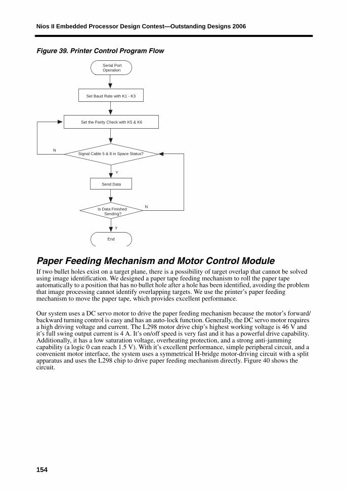
Figure 39 shows the printer control program flow.
Table 4. Asynchronous Transmission Mode
Start Bit 0 Data Bit Parity Bit Stop Bit1 bit 7/8 1 1
Table 5. Marking Handshake Mode
Handshaking Mode Data Direction RS-232C Interface SignalMarking Control Data input is allowed Signal cable 5 and 8 in space status
Data input is not allowed Signal cable 5 and 8 in mark status
Table 6. General Command Codes
Command Code Format DescriptionHex Decimal Hex
00 0 00 n Choose the character set 1 or 2: n = 01, 02.
0A 10 0A Press the Enter key to start a new row.
0D 13 0D Press the Enter key to start a new row, the command ends.
0E 14 0E n Reprint the code before 0E for n times.
153
Nios II Embedded Processor Design Contest—Outstanding Designs 2006
Figure 39. Printer Control Program Flow
Paper Feeding Mechanism and Motor Control ModuleIf two bullet holes exist on a target plane, there is a possibility of target overlap that cannot be solved using image identification. We designed a paper tape feeding mechanism to roll the paper tape automatically to a position that has no bullet hole after a hole has been identified, avoiding the problem that image processing cannot identify overlapping targets. We use the printer’s paper feeding mechanism to move the paper tape, which provides excellent performance.
Our system uses a DC servo motor to drive the paper feeding mechanism because the motor’s forward/backward turning control is easy and has an auto-lock function. Generally, the DC servo motor requires a high driving voltage and current. The L298 motor drive chip’s highest working voltage is 46 V and it’s full swing output current is 4 A. It’s on/off speed is very fast and it has a powerful drive capability. Additionally, it has a low saturation voltage, overheating protection, and a strong anti-jamming capability (a logic 0 can reach 1.5 V). With it’s excellent performance, simple peripheral circuit, and a convenient motor interface, the system uses a symmetrical H-bridge motor-driving circuit with a split apparatus and uses the L298 chip to drive paper feeding mechanism directly. Figure 40 shows the circuit.
Serial PortOperation
Set Baud Rate with K1 - K3
Set the Parity Check with K5 & K6
Signal Cable 5 & 8 in Space Status?N
Y
N
Y
Send Data
Is Data Finished Sending?
End
154

Automatic Scoring System
Figure 40. L298 Motor Driving Circuit
System Clock Service ModuleTo implement the shooting timing, the system uses the system clock service on the human-machine interaction back-end to generate an electronic clock service. Typically, when creating an electronic clock service with a single-chip microcomputer, the system first initializes the timer, selects a 1-second timer (or some other timer), counts using a counter, and uses 1 second interrupts. However, with a Nios II processor, we do not need to run this program on the hardware application layer (HAL) because the processor takes care of the initialization process and related hardware details. Instead, we start the system clock service, which generates an alarm event every other second and adds a 1 to the number of seconds in the callback function. Figure 41 shows the system clock service procedure.
Figure 41. System Clock Service Flow
Start
Call alt_alarm_start to Startthe System Clock Service
Add a 1 to the Number of Seconds in the Call-back Function my_alarm_callback & Send Signal Volume add_second_sem
Call alt_alarm_stop to Stop the System Clock Service
End
Call process_timer_task to Process theCarry of Seconds, Minutes & Hours
155

Nios II Embedded Processor Design Contest—Outstanding Designs 2006
The HAL provides the following steps for using the system clock service:
1. Call alt_alarm_start() to start the system clock service.
2. Compile the callback function according to the format requirements (the function implements the user-defined function).
3. Call alt_alarm_stop() to stop the system clock service.
To build the time interaction setting, our system uses the DE2 development board’s four buttons. This function mainly implements the system operation status and time setting/control (e.g., setting the date and time), and controls the Nios II back end start, stop, and reset. We had to figure out how to use only 4 buttons for all of the functions: we used different statuses to implement different functions.
In the Nios II CPU, we distribute the RESET pinout to the development board’s KEY0. KEY0 implements the Nios II system back-end reset function. KEY1, KEY2, and KEY3 implement the date and time setting and some other control functions. Table 7 shows the button functions.
When implementing the program, we determined the status first and then the key value. We implemented various functions according to different key values. See Figure 42.
Table 7. Button Functions
Pin Function DistributionKEY0 Reset of the whole Nios II system back end.
KEY1 Run control status. Setting status: add 1.
KEY2 Stop control status. Setting status: subtract 1.
KEY3 Change status button.
156

Automatic Scoring System
Figure 42. Interaction Setting Flow
Speaker ModuleThe speaker module makes the system more personalized and automated. We save the speaker data in the SD memory card and transfer it to the 24-bit audio codec using the SD card read operation for audio playing.
The multifunctional SD memory card provides large capacity, high performance, and excellent security. SD cards were developed by Panasonic, Toshiba, and Sandisk based on the multimedia card (MMC) card, which have been used in digital cameras, personal digital assistants (PDAs), mobile phones, and other portable devices.
SD Memory Card Bus ProtocolThe SD memory card protocol is question-answer. The host sends a command (CMD) and the card sends a response (RES). If there is data to be transferred, it is sent on the DATA line. The SD card has 34 commands, including copyright protection commands (26 basic and 8 special commands). The CMD command format is predefined (see Figure 43).
Start
Initialize the Button, Register Button Interrupt & Start the Interrupt
Interrupt the Service Program to Obtain the KeyValue. Send the Signal Volume to
get_key_value_sem
Start process_key_data_task to PerformDifferent Processing According to the
Key Value
Determine Status
Set Run or Stop Status Set Year, Month & Day Status Set Hour & Minute Status
Judge key_value
Key 1 Key 2 Key 3Key 1 Key 2 Key 3Key 1 Key 2 Key 3
CloseRS-485Interrupt
StartRS-485Interrupt
Enter intoSet YearStatus
Add 1 tothe Year,Month &
Day
Subtract1 from
the Year,Month &
Day
Enterinto the
NextStatusin Turn
Add 1 toHour &Minute
Subtract 1 fromHour &Minute
Enterinto the
NextStatusin Turn
Judge key_valueJudge key_value
157

Nios II Embedded Processor Design Contest—Outstanding Designs 2006
Figure 43. SD Card Command Format
The SD card responds to four formats, R1, R2, R3, and R6. All commands have a specified response except CMD 0. Figure 44 shows the R1 response format; other response formats are similar to R1—the only difference is the length and information carried.
Figure 44. R1 Response Format
Refer to SD memory card specifications for more information on the commands, responses, and information carried.
SD Memory Card Register DescriptionThe SD card configuration process is the read/write process of the SD card register. The card identification (CID), card-specific data (CSD), and operation conditions register (OCR) are the key registers. Table 8 describes the register function.
SD Memory Card InitializationSD card initialization generally includes following steps:
1. Check whether the card is inserted.
2. Rest the control module and card.
3. Check the card’s type.
4. Validate the card’s voltage.
5. Get the card’s CID.
Bit Position 17 16 [15:10] [39:8] [7:1] 0
Width (Bits)Value
1‘0’
1‘0’
6x
32x
7x
1‘1’
Description Start Bit Transmission Bit Command Index Card Status CRC7 End Bit
Table 8. SD Card Register Description
Register FunctionCID Include the card manufacturer and version information.
CSD Include card capacity information, block size, and whether write protection is enabled.
OCR Include the card operation voltage information. Can set the card’s working voltage by reading/writing the register.
Transmitter Bit:'1' = Host Command
Start Bit:Always '0'
0 1 Content CRC 1
Command Content: Command & Address Informationor Parameter, Protected by 7-Bit CRC Checksum
End Bit:Always '1'
Total length = 48 Bits
158

Automatic Scoring System
6. Distribute the relative card address (RCA).
7. Set the data’s read/write block size.
SD Memory Card Read/Write OperationSD cards are usually read/written using the data block mode (BLOCK). Each read/write is an integer multiple of BLOCK. The CMD17/CMD18 and CMD24/CMD25 commands read one or more or write one or more data blocks, respectively. The data has a CRC at the end. If validation fails, the transferred data is discarded and the data read/write operation is also suspended.
Audio Encoding/DecodingThe DE2 board has the WM8731 audio encoding/decoding device, which supports 24-bit multi-bit sigma triangle analog-to-digital (A/D) and digital-to-analog (D/A) conversion, and an A/D converter (ADC) and D/A converter (DAC), all of which support inserting a digital value, 16 to 32 bits, a sampling rate of 8 to 96 kHz, stereo audio output with data cache, and digital volume adjustment. The CPU controls the chip via the I2C bus.
I2C Bus OverviewThe I2C serial bus is composed of an SDA data cable and SCL clock, which can send and receive data between the CPU and components it controlls. The maximum transfer speed between components is100 kbps. All controlled components, each of which has a unique address, are connected to the bus in parallel. During information transfer, the host controller’s control signal includes the address code and control volume. The address code selects the address, i.e., it selects the components that are expected to provide control. Therefore, all control components are on the same bus but independent of each other.
Speaker ImplementationWe include three SOPC Builder modules for the SD card, I2C bus, and audio modules. The SD card module provides data, clock, and commands using three programmable I/Os (PIOs): SD_DAT, SD_CLK, and SD_CMD. The I2C module connects to the CPU and the audio encoding/decoding device, and allows the CPU to control the audio encoding/decoding device. The audio module contains the following functions:
■ User-defined peripheral Audio_0—Provides data processing and time sequence synchronization. The module’s clock is generated by the 27-MHz external crystal oscillator using a phase locked loop.
■ AUD_FULL PIO—Generates a high-level signal when the audio encoding/decoding device data register is full. Every time it writes data to the WM8731 device’s data register, it first queries whether it is a low level. Because the SD card’s data reading speed is not the same as theWM8731 device’s decoding speed, we use another 512-byte buffer area to save the data read from SD card.
Figure 45 shows the audio playback flow.
159

Nios II Embedded Processor Design Contest—Outstanding Designs 2006
Figure 45. Audio Playback Program Flow
μC/OS-IIThe embedded system is important technology that is widely used in communications. It has greatly enhanced people’s quality of life and affected their lifestyle. An embedded OS is system software that runs on an embedded hardware platform and provides unified coordination, operation, and control over the system and its components. Because of it’s hardware features, diversified application environment, and unique development approach, an embedded OS is very different from an ordinary OS. Embedded OS’s have the following features:
■ Small size
■ Can be clipped
■ Real-time operation
■ High reliability
■ Portability
Start
initialize SD Card
Read Data with Data Block (512 Bytes) tothe Buffer Area
Is AUD_FULL at a Low Level?
N
Y
N
Y
Write 16-Bit Data to Audio_0
Is the Data BlockFinished Writing?
End
Read Data of the Next DataBlock to the Buffer Area
160

Automatic Scoring System
Featuring small size, high efficiency, real-time personal customization, ROM storage, etc, the embedded system is widely used in a variety of fields. Generally, the embedded OS provides the following three services to help application designers:
■ Memory management—Assigns and releases the memory for the application so that the memory can be used repeatedly.
■ Multi-tasking management—Provides a good task schedule mechanism, controlling the start, operation, suspension, ending, etc. tasks.
■ Peripheral management—Schedules and manages peripherals such as the keyboard, display, communication port, peripheral controller, etc.
Comparing μC/OS-II and μCLinuxμC/OS-II and μCLinux are both excellent embedded operating systems. They have good performance and open source code, however, one is real-time and the other is not. μC/OS-II is a real-time OS that is applicable to small control systems. It has high efficiency, a delicate structure, real-time operation, good scalability, etc. μCLinux is not real-time and it has the advantages of Linux. It is specifically designed for embedded processors: it has built-in network protocols and supports multiple file systems, and includes Linux advantages such as stability, powerful network capability, and an excellent file system.
Table 9 compares μC/OS-II and μCLinux in terms of real-time operation, task schedules, file system support, and system portability.
Our system has a strong real-time requirement and only needs a small control system, therefore, we used μC/OS-II, which is sufficient to perform the required tasks.
μC/OS-II IntroductionμC/OS-II is a priority-based, hard, preemptive real-time kernel, and has gained acceptance worldwide since its launch in 1992. The kernel is designed for embedded devices and has been ported to over 40 CPUs with different structures and 8- to 64-bit systems. The system has authenticated by the American FAA since version 2.51, and can run on very demanding systems such as aircrafts. μC/OS-II source code is available for free, which is, undoubtedly, the most economical choice for an embedded RTOS. Figure 46 shows the μC/OS-II system structure.
Table 9. Comparing μC/OS-II and μCLinux
Feature μC/OS-II μCLinuxReal-time operation Supports real-time operation. Does not support real-time operation.
Task schedules Has preemptive schedules. When a higher priority task occurs in the ready state, the schedule immediately suspends the current task’s operation (places it in the ready state) and assigns the CPU to the higher priority task.
Has non-preemptive schedules using a time slice service. The system initiates the tasks at some interval while generating quick and periodic interrupts to determine the function schedule (when the program can get its time slice).
File system support Has no support. Uses the romfs file management system.
System portability Very simple. Altera has ported μC/OS-II to the Nios II platform.
Comparatively complex and divided into structure level, platform level, and board-level portability.
161

Nios II Embedded Processor Design Contest—Outstanding Designs 2006
Figure 46. μC/OS-II System Structure
μC/OS-II TasksThe μC/OS-II kernel manages and schedules tasks. It can manage up to 64 tasks, including 8 system tasks and 56 user tasks. Each task is composed of a task control module, stack, and code. The task control module records the tasks’ stack pointer, current state, priority etc., connecting the task code and stack. To manage multi-tasking, μC/OS-II links all system task control modules together, forming two task chains that manage the task control module, which performs relevant operations. The task stack saves information in the CPU register or the task’s private data when the task switches or the response is interrupted. The task code implements user-defined functions, and it is an infinite cycling structure. Figure 47 shows the code for a task with an infinite cycling structure.
Figure 47. Compiled C Language Task
μC/OS-II has a preemptive task schedule, which keeps the highest priority task in a ready state and running all the time. μC/OS-II schedules the tasks according to the ready task list and the task scheduler schedules the detailed tasks. The task scheduler looks in the ready task list for the highest priority task in ready state and switches tasks. μC/OS-II has two types of task schedulers: a task-level scheduler and an interrupt-level scheduler. The task-level scheduler uses the OSSched() function and the interrupt-level scheduler uses the OSIntExt() function.
μC/OS-II InterruptsSimilar to an ordinary MCU, μC/OS-II response interrupts support interrupt nesting. The Nios II HAL interrupt is compatible with μC/OS-II, therefore, the Nios II HAL can run on μC/OS-II with a slight modification. Of particular note is that the μC/OS-II kernel is preemptive: after completing the interrupt service program, the system runs the highest priority task in the ready state, if necessary, instead of the interrupted task.
User's Application Program
Code Explaining Irrelevancebetween μC/OS-II & Processor
Code Explaining Relevance between
μC/OS-II & ApplicationProgram
OS_CFG.HINCLUDES.H
OS_CORE.COS_FLAG.COS_MBOX.COS_MEM.COS_MUTEX.C
OS_Q.COS_SEM.COS_TASK.COS_TIME.CUC/OS-II.CUS/OS-II.H
CPU Timer
Software
Hardware
μC/OS-II
Code Explaining Relevancebetween μC/OS-II & Processor
(Must Be Modified when Transplanted)
OS_CPU.HOS_CPU_A.ASMOS_CPU_C.C
162

Automatic Scoring System
When compiling the μC/OS-II interrupt service, we use the following functions:
■ OSIntEnter() is the interrupt entering function and it usually occurs after the interrupt service program’s interrupted data but before the user’s interrupt service code operation. It adds a 1 to the OSIntNesting global variable to record the interrupt nesting layers.
■ OSIntExit() is the interrupt service out function. It subtracts a 1 from the OSIntNesting global variable and switches the ready-to-operate task if OSIntNesting is 0. If the scheduler is not locked up and the ready task list’s highest priority task is not the interrupted task, it returns to the interrupted service sub-program.
Synchronization and Communication of μC/OS-II TasksWhen performing multiple tasks, the OS must resolve two problems:
■ The shared resource can only be accessed by one task at one moment, that is, the tasks are mutually exclusive.
■ The tasks must be executed in order to perform task synchronization.
Solving these problems requires communication between the tasks. μC/OS-II achieves this communication by signal traffic, e-mail, and a message queue. Simple signal traffic communicates between the system tasks, which is what we describe here.
Signal traffic was invented in the mid 1960s. It controls access to the shared resource, presents events, and synchronizes two tasks. The μC/OS-II signal traffic operations include establishing, waiting, and delivering signal traffic, using the OSSemCreate(), OSSemPend(), and OSSemPost() functions, respectively. The initial values must be provided when the signal traffic is established. The initial value is one of three types:
■ 0—The signal traffic represents the occurrence of a event.
■ 1—The signal traffic controls access to shared resources.
■ n—The signal traffic stands for the number of resources available to be accessed.
When multiple tasks are waiting for the same signal traffic, μC/OS-II always gives it to the highest priority task.
μC/OS-II Task ArchitectureIn this system, the OS operates on the athlete side, and receives, processes, displays, and prints the matches results (7 tasks, 6 traffic signals, and 5 interrupts). Table 10 shows the task functions.
Table 10. Task Functions
Task Function Descriptioninitialize_task() Father task. Performs self-cancellation after initializing signal traffic and
establishing task functions.
process_key_data_task() Addresses differently according to different key values.
process_timer_task() Manages the date and time.
process_data_task() Processes the data received by wired or wireless cable. Gets the X, Y coordinates and circular number.
Wireless_receive_task() Initializes the wireless receiving module, opens a wireless receiving interrupt, and closes the wired receiving interrupt.
163

Nios II Embedded Processor Design Contest—Outstanding Designs 2006
Table 11 shows the signal traffic functions.
Figure 48 shows the μC/OS-II OS flow chart.
lcd_show_task() Controls the LCD target surface, sets the target, and displays the circular number.
printer_task() Prints the match results.
speaker_task() Reports the target shooting via audio.
Table 11. Signal Traffic Functions
Signal Traffic Functionadd_second_sem Sent by the system clock service’s callback function my_alarm_callback() to
notify process_timer_task() of time processing.
get_key_value Sent by the key interrupt service sub-program button_isr(). Notifies process_key_data_task() that is should judge the key values and make processions.
printer_sem Sent by process_data_task(). Notifies printer_task() that it should print the match results when it obtains the circular number.
show_result_sem Sent by process_data_task(). Notifies lcd_show_task() that it should display the match results when it obtains the circular number.
get_raw_result_sem Sent by wired or wireless receiving interrupt. Notifies process_data_task() that it should process the X, Y coordinates and circular number upon receipt of the data.
start_wireless_sem Sent by the switch interrupt switch_pio_isr(). Notifies Wireless_receive_task() that it should open the wireless receiving interrupt.
speaker _sem Sent by process_data_task(). Notifies speaker _task() that it should broadcast the match results when it obtains the circular number.
Table 10. Task Functions
Task Function Description
164

Automatic Scoring System
Figure 48. μC/OS-II Procedure Flow Chart
System Testing and AnalysisThis section describes the tests we performed and discusses the results.
Target Identification TestTarget identification is the key technology of the system, and it directly affects the shooting reporting accuracy. In the actual report, the circular number refers to the shortest distance between the ring’s center and the target. Table 12 shows the test results.
We can place a light in front of the target. Our practice shots show that the system can identify the target even if the light is not very bright.
Table 12. Target Identification Test
Number of Times Circular NumberVisual Inspection System Test
1st time 4.2 to 4.4 4.2
2nd time 5.6 to 5.7 5.7
3rd time 6.5 to 6.7 6.6
4th time 7.5 to 7.8 7.6
5th time 8.6 to 8.8 8.6
6th time 9.5 to 9.7 9.6
7th time 10.4 to 10.6 10.5
Start
SystemInitialization
Establish Father TaskInitiate OS
Wait Interrupt
JudgeInterrupt
TimerInterrupt
Key PressInterrupt
Wired ReceiveInterrupt
SwitchInterrupt
Send Signal Trafficadd_second_sem
Send Signal Trafficget_key_value
Send Signal Trafficge_raw_result_sem
Send Signal Trafficstart_wireless_sem
Initiate Taskprocess_timer_task
Initiate Taskprocess_key_data_task
Initiate Taskprocess_data_task
Initiate Taskwireless_receive_task
165

Nios II Embedded Processor Design Contest—Outstanding Designs 2006
Test results—When we compared the actual measurement and the system’s measurement, the system’s target identification accuracy is up to 0.1 ring, which is sufficient to meet the demands of ordinary competitions and meets the design goal.
Target Tracking TestTo improve the system’s automation and intelligence, we introduced a closed-loop feedback control mechanism to add target tracking ability. When the athlete finishes shooting and the system identifies the target position, the paper feeding mechanism rotates the target paper downward until the target disappears. Table 13 shows the test results.
Test results—The test showed that the system can track the target until it disappears, which meets the design goal.
Wireless Transmission TestTo improve the system’s flexibility for various conditions, we added a wireless transmission module. Because correct data transmission is crucial for the competition to be fair and just, the transmission distance and error code rate are strictly required. Table 14 shows the test results.
Test results—The test showed that the error code rate is next to zero, which satisfies the system demands and meets the design goal.
RS-485 TestTo ensure correct data transmission, the system supports RS-485 transmission. The data is sent from the image processing front-end via the DE2 development board’s standard RS-232 peripheral, through shielded twisted-pair cables, through the human-machine interaction module’s RS-232 peripheral (in the background), to the DE2 development board. Table 15 shows the test results.
Table 13. Target Tracking Test
Number of Times Target Position Tracking Goal Achieved?1st time About 7 rings Yes
2nd time About 8 rings Yes
3rd time About 9 rings Yes
4th time About 10 rings Yes
Table 14. Wireless Transmission Module Test
Number of Times Data Sent Data Received1st time 305 305
2nd time 535 535
3rd time 524 524
Table 15. RS-485 Bus Transmission Test
Number of Times Data Sent Data Received1st time s240240109t s240240109t
2nd time s235245950t s235245950t
3rd time s345198580t s345198580t
166

Automatic Scoring System
Test results—The test showed that the module correctly transmits the data, which satisfies the system demands and meets the design goal.
Printer TestThe printed competition scores are the proof that rates the athletes’ performance and serves as a data back-up. To ensure that the competition is fair and just, the printed scores must be accurate with no errors. Therefore, correct data delivery, transmission, and printing is vitally important. The data is sent via the DE2 board’s standard serial port and is transmitted to a micro-printer using a serial cable. Figure 49 shows the printer and cable.
Figure 49. Printer and Cable
Table 16 shows the test results.
Test results—Comparing the actual printed data to the sent data, the printer can correctly print the competition scores, which meets the design goal.
LCD Display TestThe display is an important tool for human-machine interaction. It presents the system and competition information to the users and improves the system’s visual value. The system uses three PIOs to control the LCD, which can simultaneously display the current and past scores as well as the target position. Figure 50 shows the LCD.
Table 16. Printer Test
Number of Times Data Sent Data Printed1st time 1 1
2nd time 2 2
3rd time a a
4th time b b
167

Nios II Embedded Processor Design Contest—Outstanding Designs 2006
Figure 50. LCD
Table 17 shows the test results.
Test results—The test shows that the LCD module can display the current and past scores as well as the target position, which meets the design goal.
Design FeaturesOur design has the following features.
■ With the approach of the 2008 Beijing Olympic Games, we combined advanced FPGA technology and an embedded SOPC with shooting to built a cheap, applied, intelligent, highly integrated auto riflery scoring system.
■ We convert the machine vision and template matching into practice and perform bullet hole positioning and recognition.
■ The system combines software and hardware to build the design in one FPGA.
■ Implementing image processing in hardware greatly improves the response speed and is important for image processing in ASICs.
■ The system applies software radio technology, adds the wireless transmission function, and enhances system flexibility.
Table 17. LCD Display Test List
Number of Times Data Sent Data Displayed1st time X 240 X 240
Y 240 Y 240
Circular number 10.9 Circular number 10.9
2nd time X 190 X 190
Y 230 Y 230
Circular number 9.3 Circular number 9.3
3rd time X 180 X 180
Y 198 Y 198
Circular number 7.1 Circular number 7.1
168

Automatic Scoring System
■ When recognizing the bullet hole, the system introduces machine vision: using a light source design that adopts a diffused reflection in poor light to increase the hole’s brightness and adapt the light in front of the target.
■ The system pays attention to human interaction, and uses an LCD and speaker to deliver all-in-one users information.
■ Using an auto-control theory, the system introduces closed-loop feedback to adjust the system intelligently and save the maximum resources without increasing the system cost.
■ The system fully uses the Nios II processor advantages. The resources used can perform the system operation without any other controller.
■ Each part of the system is designed modularly, providing abundant peripheral interfaces for extending the system. The system provides excellent migration and utility; besides the scoring system, the application can be applied to other areas, such as image processing and software radio technology.
ThoughtsWe were very honored to participate in the Nios II contest. Not only did we learn new technology, we learned cooperation and persistance. We enthusiastically chose the automatic scoring system as our topic because we had worked on one before. In the past, however, we used a laser diode, which cannot improve precision. After participating in the contest, we decided to use audio processing. In the beginning, we knew nothing about audio processing and searched for information on the Internet and in the IEEE archives with keywords such as FPGA and IMAGE. Fortunately, we found a lot of materials and experience from others. Our algorithm originated from median filtering with an FPGA.
Of course, we did have some difficulties, e.g., the DE2 development board SDRAM was used as the camera module buffer, so our Nios II program could not run on the SDRAM. But, the FPGA’s RAM was too small, and we could only run the program on SRAM. This problem caused us difficulty for quite a long time, because the SRAM could access data in 16-bit format, but the operation program was not stable. We eventually found that if we changed the SRAM into 8-bit data format we could ensure stable program operation.
In the process of defining the custom instruction, we realized that if we did not include a custom instruction when we first built the CPU, we needed to reconstruct the CPU when we added the instruction later. We successfully migrated μClinux to the Nios II processor. But with the network and USB functions, and because we did not have to migrate a lot of programs or use network functions for our system, μC/OS-II met all of our requirements and we used it instead.
We noticed that when we combined the FPGA with the Nios II processor, the strength of the Nios II processor could be fully exerted. We could combine all of the Verilog HDL digital modules with the Nios II processor. We could select the best way to implement the whole system.
We want to thank the teachers and students who provided great support and encouragement. We want to thank Altera for the opportunity and Terasic Technologies for their support during the contest—they provided us with excellent Verilog HDL code examples that we used to learn how to create the Verilog HDL project. For example, all of the development board pinouts are defined in the top-level module. The pins are all assigned, and the following development work does not needs to worry about whether the pins have been assigned correctly, makeing development more convenient. Many of our problems had nothing to do with the technology, but they did affect the project process.
Thanks to Mr. Huang Weifeng’s (of Huazhong University of Science and Technology) image processing speech and Mr. Chen Jia’s (an excellent analog IC designer) great support. Thanks to Mr. Jin Qiang’s (from the department of mechanical engineering of Huazhong University of Science and Technology) guidance on machine design and the Huazhong University of Science and Technology’s machine factory environment support. Thanks to the great support from director Huang and Wang, the
169

Nios II Embedded Processor Design Contest—Outstanding Designs 2006
Hubei Sports Shooting Training Center coach. Thanks to the technical guidance from KZW (you must be familiar with the name if you have visited the Nios II forum). We also want to express our appreciation to the Yin and Xiao teachers from the Electrical and Electronic Innovation Center of Huazhong University of Science and Technology. We could not complete our work without the support of so many friends. This kind of work is not only a technological achievement, but it is also a collaboration many people’s efforts.
We expended a lot of effort in our work, but we cannot say it is perfect and we plan to make improvements in the future.
ConclusionOur design implements an automated scoring system for shooting sports, which provides an effective solution for target identification, data transfer, result display, and automated target sheet replacement. The design is based on template matching, closed-loop control, software-defined radio, and other leading concepts, and successfully combines with embedded SOPC technology, image processing, wireless communication, and automatic control technology. The system is adaptable and agile, and can be used in indoor/outdoor fixed target contests and training as well as field and military training. It also improves shooting training levels and automates the shooting contest management.
It took three months to complete the design and collaboration strongly with each other during the development. We learned the difference between the Nios II embedded processor and general embedded processors, and the distinctive features of embedded SOPC technology. We focused on our project unceasingly during the three months, which helped us to learn and improve.
AcknowledgementsThanks to the contest organizers, the Hubei Undergraduate Electronic Design Contest committee, Wuhan Institute of Technology, South Central University, and Altera, who gave us the opportunity to learn and use new technology, widen our view, and encourage our innovative spirit. We want to express our appreciation.
Additionally, we want to thank Huazhong University of Science and Technology for the opportunity it gave us to participate in the contest and their support during the contest.
Thanks to Yin Shi and Xiao Kan, the Electrical and Electronic Innovation Center teachers, and Chen Yongquan for their guidance and help. We also want to thank Chen Jia from the Department of Electronic Engineering of Huazhong University of Science and Technology for his guidance on the image processing module. We could not have made the design without their guidance and encouragement. We want to express our thanks and appreciation to all of them.
ReferencesBeeckler, John Sachs, Warren J. Gross. FPGA Particle Graphics Hardware. Proceedings of the 13th Annual IEEE Symposium on Field-Programmable Custom Computing Machines, 2005.
Chao, Zhang and Li Fanming. The Application of an Improved Template Matching Mode on Target Identification. Shanghai: Infrared, no. 12.
Chenglian, Peng, et al. Challenge SOC - Nios II-based SOPC Design and Practice. Beijing: Tsinghua University Press, Jul., 2004.
Fenglin, Fu. Collection of Nios II Softcore Embedded Processing. Xi’an Xidian University Press, 2005.
Fuchang, Wang, Xiong Zhaofei, and Huang Benxiong. Communication Theory. Beijing: Tsinghua University Press, 2006.
170

Automatic Scoring System
Gonalez. Digital Image Processing. Beijing: Electronic Industry Press, 2003.
Inoue, Seiki. C Language Practical Image Processing. Beijing: Science Press, 2003.
Jianbo, Zhang, Lu Chaoyang, Gao Xiquan, and Ding Yumei. A Method to Improve the Shooting Automatic Scoring System Accuracy. Xi’an: Journal of Xidian University (Natural Science Edition), Jun., 2002.
Jihua, Wu and Wang Cheng. Altera FPGA/CPLD Design (Advanced). Beijing: People’s Post and Telecommunication Press, Jul., 2005.
Labrosse, J. J., et al. Translated by Shao Beibei, etc. μC/OS-II: Source Code Opened Real Time Embedded OS. Beijing: China Electric Power Press, 2001.
Ligong, Zhou, et al. Nios II SOPC Embedded System Development Guide. Guangzhou: Guangzhou Zhouligong SCM Development Co., Ltd, 2005.
Lili, Chen, Jia Yunhe, Zhao Kongxin, and Qian Feng. The Designing and Realizing of Portable Wireless Automatic Scoring System. Beijing: Science Technology and Engineering, May, 2005.
National Undergraduate Electronic Design Contest Committee. Collection of Work of National Undergraduate Electronic Design Contest Winners (2001). Beijing: Beijing Institute of Technology Press, 2003.
Peng, Song, Jiang Jie, and Zhang Guangjun. Application of FPGA Apparatus with Embedded ARM Core on Image Detection. Nanjing: Industrial Control Computer, vol. 18, no. 5, 2005.
Shujun, Guo, Wang Yuhua, and Ge Renqiu. Embedded Processor Theory and Application - Nios II System Design and C Language Programming. Beijing: Tsinghua University Press, Jun., 2004.
Song, Pan, Huang Jiye, and Zeng Yu. Practical Course of SOPC Technology. Beijing: Tsinghua University Press, 2005.
Suwen, Zhang. High Frequency Electronic Circuits. 4th ed. Higher Education Press, 2004.
Wei, Zhang and Gao Hang. The Designing and Realizing of Image Processing Technology-based Automatic Scoring System. Nanjing: Journal of Nanjing University of Aeronautics and Astronautics, no. 12, 2000.
Xiren, Xie. Computer Network. 4th ed. Beijing: Electronic Industry Press, 2003.
Yamaoka, K., T. Morimoto, H. Adachi, T. Koide, and H. J. Mattausch. Image Segmentation and Pattern Matching Based FPGA/ASIC Implementation Architecture of Real-Time Object Tracking. IEEE, 2006.
Zhe, Ren. The Principal and Application of Embedded Real Time OS μC/OS-II. Beijing: Beijng University of Aeronautics and Astronautics Press, 2005.
Zimei, Xie. Electronic Circuit Design, Experiment & Measurement. 2nd ed. Wuhan: Huazhong University of Science and Technology Press, 2000.
Altera Nios II documentation and forums.
Appendix: CodeRefer to the PDF of this paper on the Altera web site at http://www.altera.com for code that was created for this project.
171

Nios II Embedded Processor Design Contest—Outstanding Designs 2006
172

Automatic Scoring System
Appendix 1 Image process unit module verilog code module PE( idata, odata_bak, odata_result, clk, rst_n); input clk; input [9:0]idata; input rst_n; output reg[9:0]odata_bak; output reg[9:0]odata_result; always@(posedge clk or negedge rst_n) if(!rst_n) begin odata_bak<=0; odata_result<=10'h3ff; end else begin odata_bak<=idata; odata_result<=1023-idata; end endmodule
Nios II Embedded Processor Design Contest—Outstanding Designs 2006
Appendix 2 Instantiat the verilog code of template by image process unit module pe_44( clk, idata1, idata2, idata3, idata4, rst_n, total_threshold, ); output [15:0]total_threshold; input clk; input [9:0]idata1,idata2,idata3,idata4; input rst_n; //internal wire [9:0]q11,q12,q13,q14,q21,q22,q23,q24,q31,q32,q33,q34,q41,q42,q43,q44; wire [9:0]result11,result12,result13,result14,result21,result22,result23,result24,result31,
result32,result33,result34,result41,result42,result43,result44; wire [15:0]total_threshod; assign total_threshold=result11+result12+result13+result14+result21+result22+result23
+result24+result31+result32+result33+result34+result41+result42+result43+result44; always@(posedge clk or negedge rst_n) if(!rst_n) begin ……. //omit end else begin ……//omit end //Instantiate the template code PE u11( .idata(idata1), .odata_bak(q11), .odata_result(result11), .clk(clk), .rst_n(rst_n)); PE u12(//The process of process unit instantiation is omitted… ); //following is omitted ……. endmodule

Automatic Scoring System
Appendix 3 Tamplate matching algorithm core verilog code module Template_matching( clk, rst_n, idata, X_Cont, Y_Cont, total_threshold, oData_me_X, oData_me_Y, oData_en, ); output reg oData_en; input clk; input rst_n; input [9:0]idata; input [9:0]X_Cont; input [9:0]Y_Cont; output [15:0]total_threshold; output reg [9:0]oData_me_X; output reg [9:0]oData_me_Y; //internal wire [9:0]idata1,idata2,idata3,idata4; //-------------- always@(posedge clk or negedge rst_n) begin if(!rst_n) begin oData_en<=0; oData_me_X<=0; oData_me_Y<=0; end else begin if(total_threshold<5000)//Filed value estimation begin oData_en<=1; oData_me_X<=X_Cont; oData_me_Y<=Y_Cont; end else begin oData_en<=0;

Nios II Embedded Processor Design Contest—Outstanding Designs 2006
oData_me_X<=oData_me_X; oData_me_Y<=oData_me_Y; end end end pe_44 u1( //image tamplate .clk(clk), .idata1(idata1), .idata2(idata2), .idata3(idata3), .idata4(idata4), .rst_n(rst_n), .total_threshold(total_threshold)); stack_4 u2( //image row shift register .data(idata), .clk(clk), .q1(idata1), .q2(idata2), .q3(idata3), .q4(idata4), .X_Cont(X_Cont), .Y_Cont(Y_Cont), .rst_n(rst_n)); endmodule

Automatic Scoring System
Appendix 4 Bullet hole tracking software code int EN_Motor_Move_For_Auto=0; //Motor move control flag bit, if it is 1, notify motor move int Time_for_auto=0; //timing number control alt_u32 my_alarm_callback(void* context) //system clock callback function { //realize the user-defined function if(Time_for_auto==1) { Time_for_auto=0; counter_for_auto=0; } counter_for_auto++; if(counter_for_auto==2){ counter_for_auto=0;EN_Motor_Move_For_Auto=0;} return 500; } //start system clock service void timer_start() { if(alt_alarm_start(&alarm_me,500,my_alarm_callback,NULL)<0) { printf("\nNo system clock available!\n"); } } void Motor_move_for_auto() //auto control motor function { if(EN_Motor_Move_For_Auto==1) { // printf("The motor start\n"); Motion_start(); } if(EN_Motor_Move_For_Auto==0) { //printf("The motor end\n"); Motion_end(); } }

Nios II Embedded Processor Design Contest—Outstanding Designs 2006
Appendix 5 Space coordinates conversion software code //work out the actual distance between the bullet hole and the blank with formula bottom2hole_v=CCD2Target_Bottom*tan((double)(480-y_cont)/(double)480*V_angle); hole2Center_Target_v=bottom2hole_v-9; CCD2hole_v=sqrt(bottom2hole_v*bottom2hole_v+CCD2Target_Bottom*CCD2Target_Bottom); hole2Center_Target_h=CCD2hole_v*tan((double)fabs(320-x_cont)/(double)320*H_angle); hole2Center_Target=sqrt(hole2Center_Target_h*hole2Center_Target_h+hole2Center_Target_v*hole2Center_Target_v); //calculate the actual ring number if(hole2Center_Target>Target_Center_half_length){ Target_num=10-(hole2Center_Target-Target_Center_half_length)/0.8; if(Target_num<0)Target_num=0;} else
Target_num=10.9-hole2Center_Target/0.55; //calculate the corresponding coordinates on the virtual target
……
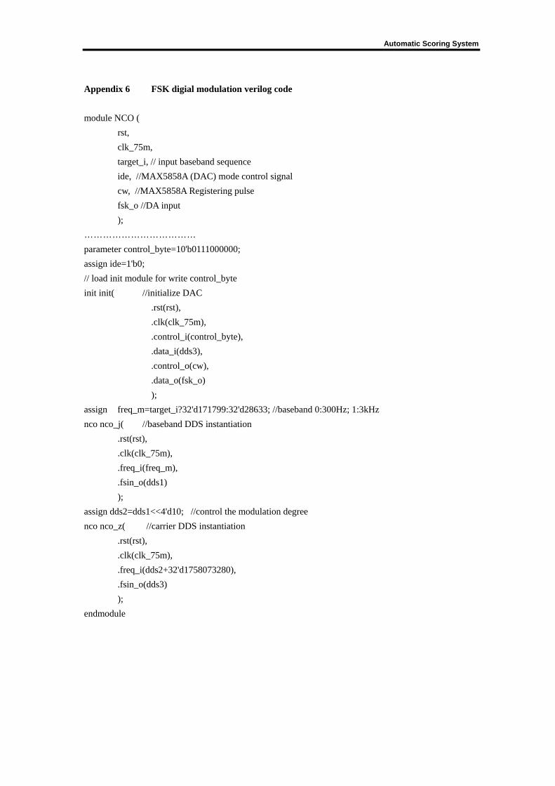
Automatic Scoring System
Appendix 6 FSK digial modulation verilog code module NCO ( rst, clk_75m, target_i, // input baseband sequence ide, //MAX5858A (DAC) mode control signal cw, //MAX5858A Registering pulse fsk_o //DA input ); ……………………………… parameter control_byte=10'b0111000000; assign ide=1'b0; // load init module for write control_byte init init( //initialize DAC .rst(rst), .clk(clk_75m), .control_i(control_byte), .data_i(dds3), .control_o(cw), .data_o(fsk_o) ); assign freq_m=target_i?32'd171799:32'd28633; //baseband 0:300Hz; 1:3kHz nco nco_j( //baseband DDS instantiation .rst(rst), .clk(clk_75m), .freq_i(freq_m), .fsin_o(dds1) ); assign dds2=dds1<<4'd10; //control the modulation degree nco nco_z( //carrier DDS instantiation .rst(rst), .clk(clk_75m), .freq_i(dds2+32'd1758073280), .fsin_o(dds3) ); endmodule

Nios II Embedded Processor Design Contest—Outstanding Designs 2006
Appendix 7 Frame header checking and the serial and parallel conversion verilog code module receive ( rst, clk, serial_i, //demodulation output endover, //external interrupt sent to the CPU target_o //coordinates information ); ……………………………… //the data information after receiving and fulfill the serial and parallel conversion (26 with 16 crc) always@(posedge clk) if(headover) begin target_p<=target_p<<1; target_p[0]<=target_buf; if(counter==25) begin endover<=1'b1; counter<=0; end else begin endover<=1'b0; counter<=counter+1'b1; end end else begin target_p<=target_p; endover<=endover; counter<=0; end //frame header checking sequence status (check the header 01010101) always@(state or serial_i or counter) case(state) 0: begin headover<=1'b0; target_buf<=1'bz; nextstate<=(!serial_i)?1:0; end 1: begin

Automatic Scoring System
headover<=1'b0; target_buf<=1'bz; nextstate<=(serial_i)?2:1; end 2: begin headover<=1'b0; target_buf<=1'bz; nextstate<=(!serial_i)?3:0; end ……………………………… 6: begin headover<=1'b0; target_buf<=1'bz; nextstate<=(!serial_i)?7:0; end 7: begin headover<=1'b0; target_buf<=1'bz; nextstate<=(serial_i)?8:1; end 8: begin headover<=1'b1; target_buf<=serial_i; nextstate<=!(counter==25)?8:0; end default: begin headover<=1'b0; target_buf<=1'bz; nextstate<=0; end endcase //********************************************************* Endmodule

Nios II Embedded Processor Design Contest—Outstanding Designs 2006
Appendix 8 CRC coding verilog code module crc ( rst, clk, target_i, crc_o ); ……………………………… reg xor_flag,add_flag,sft_flag,finish_flag; //define the marks of nonequivalence, counting, shift, and finish parameter Polynomial=17'b11000000000000101; //CRC-16 //********************************************************* assign crc_o={target_i,crc}; //********************************************************* //always@(xor_flag or sft_flag) always@(posedge clk) begin case({xor_flag,sft_flag}) 2'b00:crc_reg<=crc_reg; 2'b01:crc_reg<={crc_reg[15:0],1'b0}; 2'b10:crc_reg<=crc_reg^Polynomial; 2'b11:crc_reg<={target_i[7:0],9'h000}; default:crc_reg<=crc_reg; endcase end //********************************************************* //always@(add_flag or finish_flag) always@(posedge clk) begin case({add_flag,finish_flag}) 2'b00: begin counter<=counter;crc<=crc; end 2'b01: begin counter<=counter;crc<=crc_reg[16:1]; end 2'b10: begin counter<=counter+1'b1;crc<=crc; end 2'b11: begin counter<=4'h0;crc<=16'h0000; end default: begin counter<=counter; crc<=crc; end endcase end //********************************************************* always@(state or counter or crc_reg[16]) begin case(state) 0:

Automatic Scoring System
begin xor_flag<=1; sft_flag<=1; add_flag<=1; finish_flag<=1; nextstate<=1; end 1: begin xor_flag<=0; sft_flag<=0; add_flag<=0; finish_flag<=0; nextstate<=(crc_reg[16]==1'b1)?2:3; //judge whether the initial bit is 1 end ……………………………… 4: begin xor_flag<=0; sft_flag<=0; add_flag<=0; finish_flag<=0; nextstate<=(counter==10)?5:1;//if 9 “0” are moved in end ……………………………… 7: begin xor_flag<=0; sft_flag<=0; add_flag<=0; finish_flag<=0; nextstate<=7; end default: begin xor_flag<=0; sft_flag<=0; add_flag<=0; finish_flag<=0; nextstate<=0; end endcase end

Nios II Embedded Processor Design Contest—Outstanding Designs 2006
endmodule

Automatic Scoring System
Appendix 9 LCD source program void show_bamian() //display the target {
int x_row,y_line; ……………… unsigned int shift_mask; //shift code ………………
for(x_row=0;x_row<480;x_row++) { y_line=0; set_xy(x_row,y_line); //set X and Y coordinates before writing display data for(i=0;i<20;i++) { shift_mask=0x80000000; for(j=0;j<32;j++) { if(Pic[x_row][i]&shift_mask) //the relevant pixel point is 1, display as yellow write_data(0xfc); else write_data(0xe0); //otherwise display as red shift_mask=shift_mask>>1; //the shift code is left shifted 1 bit } } } }

Nios II Embedded Processor Design Contest—Outstanding Designs 2006
Appendix 10 Printer control source program void print_result(float result) { //open the serial port ……………… //the data process gets the ones place and decimal place of result ……………… send_char(0x0,uart1); //select character set 1 send_char(0x01,uart1); send_char(0x0d,uart1); //the command is end send_char(result_number,uart1); //print result number send_char(0x04,uart1); //print 4 “space” send_char(result_one,uart1); //print the number of ones place in the result send_char('.',uart1); //print radix point send_char(result_xiaoshu,uart1); //print the decimal place of result ……………… }
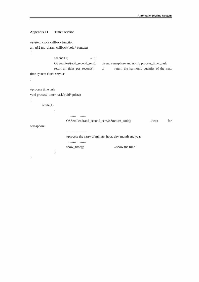
Automatic Scoring System
Appendix 11 Timer service //system clock callback function alt_u32 my_alarm_callback(void* context) { second++; //+1 OSSemPost(add_second_sem); //send semaphore and notify process_timer_task return alt_ticks_per_second(); // return the harmonic quantity of the next time system clock service } //process time task void process_timer_task(void* pdata) { while(1) { ……………… OSSemPend(add_second_sem,0,&return_code); //wait for semaphore ……………… //process the carry of minute, hour, day, month and year ……………… show_time(); //show the time } }

Nios II Embedded Processor Design Contest—Outstanding Designs 2006
Appendix 12 Key processing source program void process_key_data_task(void* pdata) { while(1) { OSSemPend(get_key_value,0,&return_code); //wait for getting key value semaphore switch(status) { case ctrl_status: switch(key_value) //carry out different process according to various key value and press KEY3 to enter set_year break; case set_year: switch(key_value) //carry out different process according to various key value and press KEY3 to enter set_month break; case set_month: switch(key_value) //carry out different process according to various key value and press KEY3 to enter set_day break; case set_day: switch(key_value) //carry out different process according to various key value and press KEY3 to enter set_hour break; case set_hour: switch(key_value) //carry out different process according to various key value and press KEY3 to enter set_minute break; case set_minute: switch(key_value) //carry out different process according to various

Automatic Scoring System
key value and press KEY3 to enter ctrl_status break; default: //ctrl_status is default break; }//switch }//while(1) }

Nios II Embedded Processor Design Contest—Outstanding Designs 2006
Appendix 13 Format conversion program Project.exe void __fastcall TForm1::Button1Click(TObject *Sender) { //select the conversion storage mode ……………… //distribute memory space for the generated file to get file path //open the image file //get the image length and width ……………… unsigned int data=0; // the initialized data bit is o for(int i=0;i<height;i++) { for (int j=0;j<width;j++) { if (Pic->Canvas->Pixels[j][i]!=0) // if the pixel point is not black, enter 1 data|=1; if(((j+1)%ww)==0) //when the data bit is full, write the data to the file { fprintf (outfile,"%d",data); if(i!=height-1||j!=width-1) //write file information by bit fprintf (outfile,","); data=0; } data=data<<1; //data bit is left shifted 1 bit } fprintf (outfile,"\n"); } //close the file and release the memory space }

Automatic Scoring System
Appendix 14 Sound target reporting source program void sound() { BYTE Buffer[512]; /define the size of buffer …………………… SD_card_init(); //SD card initialization …………………… for() //appoint the read data block number segment { SD_read_lba(Buffer,j,1); //read a data block data to buffer while(i<512) { if(!IORD(AUD_FULL_BASE,0)) //judge whether the WM8731 data register is full { Tmp1=(Buffer[i+1]<<8)|Buffer[i]; //write 16-bit data to AUDIO_0 IOWR(AUDIO_0_BASE,0,Tmp1); i+=2; } j++; //data block number +1 i=0; } } }