automated channel assessment for single chip medradio
TRANSCRIPT

Portland State University Portland State University
PDXScholar PDXScholar
Dissertations and Theses Dissertations and Theses
Spring 6-14-2013
Automated Channel Assessment for Single Chip Automated Channel Assessment for Single Chip
MedRadio Transceivers MedRadio Transceivers
Mark Alexander Hillig Portland State University
Follow this and additional works at: https://pdxscholar.library.pdx.edu/open_access_etds
Part of the Biomedical Commons, Electronic Devices and Semiconductor Manufacturing Commons,
Equipment and Supplies Commons, and the Signal Processing Commons
Let us know how access to this document benefits you.
Recommended Citation Recommended Citation Hillig, Mark Alexander, "Automated Channel Assessment for Single Chip MedRadio Transceivers" (2013). Dissertations and Theses. Paper 1005. https://doi.org/10.15760/etd.1005
This Thesis is brought to you for free and open access. It has been accepted for inclusion in Dissertations and Theses by an authorized administrator of PDXScholar. Please contact us if we can make this document more accessible: [email protected].

Automated Channel Assessment for Single Chip MedRadio Transceivers
by
Mark Alexander Hillig
A thesis submitted in partial fulfillment of the requirements for the degree of
Master of Science in
Electrical and Computer Engineering
Thesis Committee: Fu Li, Chair
Marek A. Perkowski James E. Morris
Portland State University
2013
Page i of vii
Abstract
Modern implantable and body worn medical devices leverage wireless telemetry
to improve patient experience and expand therapeutic options. Wireless medical
devices are subject to a unique set of regulations in which monitoring of the
available frequency spectrum is a requirement. To this end, implants use
software protocols to assess the in-band activity to determine which channel
should be used. These software protocols take valuable processing time and
possibly degrade the operational lifetime of the battery. Implantable medical
devices often take advantage of a single chip transceiver as the physical layer for
wireless communications. Embedding the channel assessment task in the
transceiver hardware would free the limited resources of the microprocessor.
This thesis proposes hardware modifications to existing transceiver architectures
which would provide an automated channel assessment means for implantable
medical devices. The results are applicable beyond medical device applications
and could be employed to benefit any low-power, wireless, battery-operated
equipment.

Page ii of vii
Acknowledgements
I would like to thank Micro Systems Engineering Incorporated for providing me
the resources needed to complete this thesis. Special thanks to Brian Sutton and
Paul Stadnik for guidance through its development.
I would also like to acknowledge the guidance of Dr. Fu Li throughout my
graduate studies and thesis. Additional thanks to Dr. Marek Perkowski and Dr.
James Morris for participating on my thesis committee.

Page iii of vii
Table of Contents
1. Introduction .................................................................................................... 1
2. Single Chip Radio Technology....................................................................... 3
2.1. Receiver Structure................................................................................... 3
2.2. Power Usage in Single Chip Transceivers .............................................. 5
2.3. Channel Assessment............................................................................... 7
3. CCA System Requirements ........................................................................... 9
3.1. MedRadio Requirements......................................................................... 9
3.2. Channel Assessment Time.................................................................... 10
3.3. Channel Assessment Protocol .............................................................. 12
4. Channel Assessment Means ....................................................................... 14
4.1. Down-Converting Mixer ......................................................................... 15
4.2. Frequency Source ................................................................................. 16
4.3. Power Detector...................................................................................... 17
4.4. Control Output and Measurement ......................................................... 17
4.5. Digital Control........................................................................................ 18
4.6. Hardware Impact on Transceiver Size................................................... 21
4.7. CCA System Hardware ......................................................................... 22
4.8. Hardware Timing Considerations .......................................................... 23
4.9. Signal Power Level and Power Consumption Considerations............... 24
5. CCA System Performance ........................................................................... 26
5.1. CCA Test Setup and Conditions............................................................ 26
5.2. Timing Confirmation .............................................................................. 28
5.3. Characterization Results ....................................................................... 32
5.4. Packet Test Results............................................................................... 36
5.5. Threshold Detection Vs. Channel Energy Assessment ......................... 39
6. Possible Improvements to the CCA System ................................................ 41
6.1. Scan Rate.............................................................................................. 41
6.2. Mixer Type Selection............................................................................. 41
6.3. Multi-Level Reporting or Automatic Threshold Adjustment.................... 42
6.4. Integration with the Larger Transceiver System .................................... 42
7. Conclusion ................................................................................................... 44
8. References................................................................................................... 45
Appendix A. Verilog Source Code for Clear Channel Assessment ..................... 50
Appendix B. Schematics for RF, DAC, and ADC Hardware................................ 54

Page iv of vii
Tables
Table 1 - A comparison of the apparent architecture of 13 commercial chip transceivers. ......................................................................................................... 4
Table 2 - The stated current consumption for various operating modes for each of the chip transceivers studied. ............................................................................... 6
Table 3 - CCA packet test performance with 34-channels.................................. 38
Table 4 - CCA packet test performance with 12-channels.................................. 39

Page v of vii
Figures
Figure 1 -The direct-conversion reciever architecture. ......................................... 4
Figure 2 - Limiter amplifier chain for receiver gain control. ................................... 5
Figure 3 - Hypothetical, three-part, bidirectional protocol for a two-node MedRadio network.............................................................................................. 11
Figure 4 – Potential measurement points within a channel. ............................... 13
Figure 5 - An unsuppressed image signal from a DSB mixer appearing in the IF filter bandwidth. .................................................................................................. 16
Figure 6 - Block diagram of the study system..................................................... 18
Figure 7 - Block diagram of the digital control hardware..................................... 20
Figure 8 - State flow diagram of the hardware finite state machine (FSM). ........ 21
Figure 9 - CCA System hardware....................................................................... 24
Figure 10 - Test setup used to evaluate the proposed CCA system................... 27
Figure 11 - SMIQ controller software written in C# for packet testing................. 28
Figure 12 - Accumulated spectrum for the VCO output with 12 channels. ......... 29
Figure 13 - Accumulated spectrum for the VCO output with 34 channels. ......... 30
Figure 14 - DAC/ADC write/read timing and VCO output using 34 channels. .... 31
Figure 15 - DAC/ADC write/read timing and VCO output using 34 channels. .... 32
Figure 16 – The WCDMA test signal and the CCA system. ............................... 34
Figure 17 - The Bluetooth modulated test signal and the CCA system output. .. 35
Figure 18 – The 2FSK test signal and the CCA system output. ......................... 36

Page vi of vii
Equations
Equation 1 - Detection threshold of occupied channels in the 402-405 MHz band............................................................................................................................ 10
Equation 2 - Carson's bandwidth rule and the resulting detection threshold. ..... 10

Page vii of vii
Acronyms and Abbreviations
ADC analog to digital converter ASK amplitude shift key CCA clear channel assessment CMOS complementary metal oxide semiconductor DAC digital to analog converter DSB double-sideband mixer FPGA field programmable gate array FSK frequency shift key IF intermediate frequency kbps kilobits per second kHz kilohertz LBT listen-before-talk LNA low noise amplifier LO local oscillator mA milliamperes MedRadio 47 CFR 95.627; 47 CFR 95.628 MHz megahertz MICS Medical Implant Communications Service ms milliseconds PLL phase-lock-loop RF radio frequency RSSI received signal strength indicator RX receive SSB single side-band UART universal asynchronous receiver/transmitter µs microseconds VCO voltage controlled oscillator VGA variable gain amplifier WCDMA wide band code division multiple access

Page 1 of 57
1. Introduction
Implantable and body worn medical devices are available for a wide range of
applications such as pacemakers, insulin pumps, and neurological stimulation.
These devices significantly benefit from wireless connectivity, aiding both the
physician and the patient by allowing communication with the device without the
need for physical contact or a medical office visit. With an increase in use of
wireless connectivity, the limited MedRadio frequency spectrum [1], [2] is
becoming crowded. For low-power, battery-operated, wireless nodes such as
medical devices, crowded channels can directly impact the operational lifetime of
the network [3]. As a result, clear channel assessment (CCA) techniques [4] are
of critical importance to maintaining wireless link integrity while reducing radio
on-time.
A hardware mechanism that gives insight into channel activity could provide low-
power networks a means to maintain timely access without compromising
operational lifetime. Significant research has been done in the design and study
of MedRadio transceivers [5]-[10] however, none of these efforts have
demonstrated a built-in means to perform channel assessment. Furthermore, in
the evaluation of 13 commercial single chip transceivers [11]-[23] (conducted in
this thesis), none possessed any self-contained, automated means with which to
assess their relative operating spectrum.

Page 2 of 57
This thesis proposes hardware which can be integrated with existing single chip
transceiver hardware to automate the channel assessment process with minimal
impact on overall size and complexity. Chapter 2 outlines what is available in
single chip transceiver technology for the MedRadio band and each receiver’s
hardware design. Chapter 3 discusses what an effective CCA system should
comprise. Chapter 4 covers the design of evaluation hardware for a CCA
system. Chapter 5 relates the performance of the CCA system. Chapter 6
examines how the CCA system could be extended or improved and Chapter 7
provides concluding remarks.

Page 3 of 57
2. Single Chip Radio Technology
Single chip transceivers were surveyed to understand the basic architectures
employed in these devices. Each transceiver interfaces with a host
microcontroller or microprocessor. The transceivers selected for evaluation
operate within the frequency range of 401MHz to 457MHz. This frequency range
is covered by the MedRadio regulations [1], [2] (superseding the Medical Implant
Communications Service [MICS] regulations) and provides fewer challenges to
Radio Frequency (RF) circuit design when compared with higher frequencies
such as the 915MHz and 2.4GHz industrial scientific medical bands.
Manufacturers’ datasheets were studied to determine specific elements that
comprise each device’s receiver as well as identify and evaluate key
performance metrics. Datasheets often omit explicit details of implementation but
provide sufficient information for this work.
2.1. Receiver Structure
Of the commercial transceivers studied all implement some form of direct-
conversion receiver architecture [24]. A block diagram depicting the direct-
conversion receiver is shown in Figure 1. The incoming RF signal is supplied to a
pair of down-converting mixers for incident and quadrature, driven by a local
oscillator (LO) signal at both 0° and 90° phase, respectively. The mixer output,
the intermediate frequency (IF) signal, is then filtered and amplified by a variable
gain amplifier (VGA) before being sampled by an analog to digital converter
(ADC). There is often feedback from the ADC to the VGA which allows the

Page 4 of 57
appropriate gain level to be set dynamically. In all of the transceivers studied, the
LO signal is provided by either an integer-N frequency synthesizer or a fractional-
N frequency synthesizer. Table 1 gives a comparison of the receiver structures
present in the transceivers evaluated.
Manufacturer Model # Stage 1
Stage 2
Stage 3
Stage 4
Stage 5
Stage 6
Sample Type
TI CC1120 LNA Mixer IF Amp Filter -- -- ADC
TI CC1021 LNA1 LNA2 Mixer Filter VGA ADC ADC
TI CC1020 LNA1 LNA2 Mixer Filter VGA ADC ADC
Micrel MICRF506 LNA Mixer IF Amp
SK Filter Filter -- ADC
Analog Devices ADF7020-1 LNA Mixer Filter VGA
-- -- Limiter
Nordic nRF905 LNA Mixer IF Filter --
-- -- ADC
Atmel ATA5428 LNA Mixer IF Filter
IF Amp
-- -- ADC
NXP OL2381 LNA Mixer IF Filter
IF Amp
-- -- Limiter
Silicon Labs Si4430/31/32 LNA Mixer VGA -- -- -- ADC
RFM TRC102 LNA Mixer IF Filter
IF Amp
-- -- ADC
RFM TRC105 LNA Mixer VGA Filter Filter IF Amp ADC
Maxim MAX7031 LNA Mixer VGA -- -- -- Limiter
Maxim MAX7030 LNA Mixer VGA -- -- -- Limiter
Table 1 - A comparison of the apparent architecture of 13 commercial chip transceivers.
Note: LNA = low noise amplifier
Figure 1 -The direct-conversion reciever architecture.

Page 5 of 57
Several transceivers do not sample the down-converted signal directly but
instead amplify the signal through a chain of low gain VGAs referred to as a
limiter chain [25]. At each stage, the signal level is assessed and feedback is
provided to set the gain level. Once the signal has achieved the required voltage
level, it is supplied directly to the demodulation hardware. Figure 2 shows an
example of such a limiter chain. In this receiver architecture, the received signal
strength indicator (RSSI) is proportional to the level of gain supplied by the VGA
or limiter chain. The RSSI level is used to assess the relative power of the
received signal.
Figure 2 - Limiter amplifier chain for receiver gain control.
2.2. Power Usage in Single Chip Transceivers
These transceivers are targeted primarily at low power, low cost, personal
electronics applications. Many of these applications require battery operation and
place significant emphasis on low power operation. The transmit section of these
devices will contribute significantly to the overall power consumption but is
outside the scope of this research. All of these devices have three or four
operation modes consisting of receive (RX) mode, transmit (TX) mode,

Page 6 of 57
shutdown, or idle mode where the frequency synthesizer runs continuously to
minimize startup delay. Table 2 was constructed with data from the
manufacturers’ datasheets to illustrate which section of the receiver contributes
to the overall RX mode power consumption.
MFG Model #
Lowest RX
Current (mA) Delta
Highest RX
Current (mA)
w/Synth Running
(mA)
w/Crystal Current
(mA)
No Crystal Current
(mA)
TI CC1120 17.000 5.000 22.000 -- 1.300 0.170
TI CC1021 19.900 0.000 19.900 7.500 0.500 0.077
TI CC1020 19.900 0.000 19.900 7.500 0.500 0.077
Micrel MICRF506 8.000 4.000 12.000 -- 0.780 0.280
Analog Devices ADF7020-1 17.600 2.500 20.100 -- 2.000 --
Nordic nRF905 10.500 2.000 12.500 -- 0.100 0.013
Atmel ATA5428 10.500 3.500 14.000 8.800 0.430 0.370
NXP OL2381 15.500 2.500 18.000 5.000 0.900 0.005
Silicon Labs Si4430/31/32 18.500 0.000 18.500 8.500 0.800 0.450
RFM TRC102 11.000 0.000 11.000 -- 0.600 --
RFM TRC105 2.700 0.000 2.700 1.400 0.065 0.001
Maxim MAX7031 6.700 2.000 8.700 -- -- 0.008
Maxim MAX7030 6.400 1.900 8.300 -- -- 0.008
Average 12.631 1.800 14.431 6.450 0.725 0.133
Standard Deviation 5.533 1.646 5.603 2.567 0.524 0.155
Table 2 - The stated current consumption for various operating modes for each of the chip transceivers studied.
Across the population, the average current consumption of the shutdown and idle
modes were 0.133 mA and 6.450 mA, respectively. In receive mode, some
variability is noted in current consumption primarily from the amount of gain
required in the receive chain. The average peak RX current was 14.431 mA and
the average minimum RX current was 12.631 mA with an average difference of
2.340 mA. Of the available idle mode current data, an average value of 6.450 mA

Page 7 of 57
was calculated for the population. This indicates that slightly less than half of the
RX mode current is from frequency synthesis and that the variability of supplied
current in the VGA chain is only about 16% of the peak RX mode current.
2.3. Channel Assessment
To help improve the probability of error-free communication and reduce power
consumption, communication protocols may rely on CCA to find channels with
the lowest levels of noise [4]. This is referred to as listen-before-talk (LBT) in the
MedRadio regulations. Some protocols may employ carrier sense multiple
access [26] in which a mote or node in a wireless network must contend for
available channels with other cooperative or competing nodes. As with any
communication channel, it is also possible for time-varying levels of noise to exist
as well. A channel assessment mechanism could also be used to facilitate a
channel scan when a node is searching for a cooperative node with which to
communicate.
The most straightforward means to perform CCA is to simply enter RX mode and
listen for the expected signals. If no intelligible data can be found, an RSSI level
can be used to determine if a noise source or competing signal is present in the
channel. A high RSSI level would suggest the presence of such a signal. There
are several downsides to this method. First, entering receive mode to simply
listen for a clear channel requires just as much current as receiving useful packet
data. For receivers with dynamic gain control, more current is required to listen to
channels with low to no signal levels as compared with channels where there is a
Page 8 of 57
strong, potentially identifiable signal. Another issue is that, for the majority of the
transceivers studied, no automated assessment mechanism exists. This requires
the host controller to be fully active, listening for received data and managing
channel switching as well as RSSI level assessment. This further increases
current consumption and busies the controller with additional overhead.
The only transceiver reviewed in this study that had any form of automated
channel assessment capability was the Silicon Labs Si443x. To provide this
function, the Si443x has a single register which complements the RSSI register
into which a threshold value can be written. The controller can set this threshold
level and place the transceiver into receive mode. The controller is then free to
enter a low power state. If the RSSI level exceeds the threshold level, an
interrupt mechanism can be triggered to wake the controller. This is a small
improvement but only benefits the overall current consumption by allowing the
controller to enter a lower power state and restricts the assessment to a single
channel.

Page 9 of 57
3. CCA System Requirements
In order to design an effective CCA system, it is critical to understand the types
of signals that may be present in the frequency band of interest. These include
not only wanted signals but unwanted signals as well. Unwanted signals can take
the form of noise or excessive power from devices operating in adjacent bands or
at harmonic multiples of the operating band of interest. Devices operating the
MedRadio frequency bands have well-defined operating characteristics.
3.1. MedRadio Requirements
MedRadio devices typically use medium to low data rate digital communication
with a frequency shift key (FSK) or amplitude shift key (ASK) modulation
scheme. Phase shift key (PSK) modulation is possible but, based on the
commercial transceiver offerings, not typically available. The MedRadio
regulations set limits on the power levels and the occupied bandwidth of
transmitters operating in the various bands within the 401-457 MHz range.
MedRadio devices operating in the 401-406 MHz range have a bandwidth
limitation of up to 300 kilohertz (kHz) from 402-405 MHz and 100 kHz otherwise.
The MedRadio requirements also dictate that devices operating in the 402-405
MHz band define the center channel about 403.65 MHz.
The LBT requirements for MedRadio devices state that transmitters operating in
the 402-405 MHz band must listen for 10 ms per channel, five seconds prior to
any attempt to transmit on that channel. The listening device must register a

Page 10 of 57
channel in use if the power detected in the channel exceeds a threshold given by
Equation 1.
( ) ( )dBiGHz
dBmHzB +
−150log10 10
Equation 1 - Detection threshold of occupied channels in the 402-405 MHz band.
Here B represents the widest emission bandwidth of the signal to be transmitted
and G represents the isotropic antenna gain of the transmitter. For an FSK
signal with a single-sided frequency deviation of 50 kHz and a Manchester
encoded bit rate of 48 kilobits per second (kbps), the estimated bandwidth is
approximated by Carson’s Rule (Equation 2) [27]. If the antenna gain is
assumed flat over the 402-405 MHz band at 0 dBi (dB relative to an isotropic
radiating source) the LBT detection threshold is shown in Equation 2.
( )
( )( ) dBm
ffB m
97015048000500002log10
2
10 −=+−+∗
+∆∗=
Equation 2 - Carson's bandwidth rule and the resulting detection threshold.
3.2. Channel Assessment Time
There are no access time restrictions in the MedRadio bands. Once a channel is
established between two devices, the communication session is permitted to
proceed indefinitely. However, endless communications are unlikely. It is
reasonable to assume that the majority of communications will consist of short
bidirectional sessions between two or more nodes. Consider a three-part

Page 11 of 57
bidirectional session between two nodes consisting of an initiation packet (192
encoded bit periods), a data packet (576 encoded bit periods), and an
acknowledgement packet (192 encoded bit periods). The Manchester encoded
bit rate will be 48 kbps.
Figure 3 shows the communication structure and timing for a simple two node
network. It is assumed that there is no delay for each endpoint’s transition
between receive mode and transmit although the actual delay may be some
number of bit periods. The Analog Devices ADF7020-1 transceiver datasheet
specifies this turn-around time to be roughly 252 µs at 48 kbps but this time
varies by manufacturer.
Figure 3 - Hypothetical, three-part, bidirectional protocol for a two-node MedRadio network
Assuming a hypothetical arrangement of 25 of these two-node networks, and
each individual node has effectively equal probability of detecting any other
transmitting node in the listening space. Each pair of nodes is comprised of a
sensor node and a master node that attempts to obtain data from the sensor
node every five minutes on a randomly selected channel. If the INIT packet fails
to garner a response, the master node does not retry but simply waits for another
five minutes to elapse, disregarding the time spent with its failed attempt.

Page 12 of 57
Assuming the INIT packet has 80 encoded bit periods of preamble, this protocol
provides a 1.667 ms window in which a sensor node is able to detect and
possibly decode an INIT packet from its paired master node. In contrast, an
unpaired sensor or master node has a 20 ms window in which this exchange
between any other two-node networks could be detected. This illustrates that
even with nodes that maintain synchronization between communication attempts,
a CCA mechanism that is able to quickly scan all available channels could aid in
improving network performance by not only avoiding blocked channels but
quickly identifying potentially paired nodes as well. An effective channel
assessment mechanism must to be fast enough to allow for scanning that can
capture these short duration events.
3.3. Channel Assessment Protocol
There are two basic functions of the channel assessment mechanism. The first
is to identify the least-interfered channel in accordance with an LBT protocol for a
node that wishes to transmit. The intuitive choice would be to measure the
power level directly at the center of each channel. This is true for ASK
modulation but the spectral distribution for an FSK signal would have the highest
power level concentration at some frequency deviation above and below from the
carrier frequency. The second function of the channel assessment system is to
allow a receiving node to make a best guess as to which channel to begin
listening by determining if there is a signal centered within the channel of interest.
The challenge then is that, with only measuring in the center of the channel, it
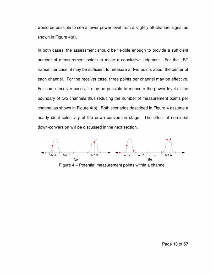
Page 13 of 57
would be possible to see a lower power level from a slightly off-channel signal as
shown in Figure 4(a).
In both cases, the assessment should be flexible enough to provide a sufficient
number of measurement points to make a conclusive judgment. For the LBT
transmitter case, it may be sufficient to measure at two points about the center of
each channel. For the receiver case, three points per channel may be effective.
For some receiver cases, it may be possible to measure the power level at the
boundary of two channels thus reducing the number of measurement points per
channel as shown in Figure 4(b). Both scenarios described in Figure 4 assume a
nearly ideal selectivity of the down conversion stage. The effect of non-ideal
down-conversion will be discussed in the next section.
Figure 4 – Potential measurement points within a channel.

Page 14 of 57
4. Channel Assessment Means
Because MedRadio devices primarily use FSK or ASK modulation and have a
limited channel bandwidth between 100 and 300 kHz, the spectral distributions
should be fairly well-defined. Detection of such a signal should be relatively
simple as well. A simple square-law power detector circuit could be employed.
In fact, this method is a typical means with which an RSSI level can be extracted
in a receiver [27]. In order to assess the in-channel power, it is important to
isolate the signal in the channel and avoid the influence of adjacent channels on
the measurement. One option is to use very selective filtering, restricting the out-
of-channel signals. The problem with very narrow, multi-pole, band-pass filters is
that the signal of interest can be greatly attenuated, calling for additional
amplification after filtering. From a low power detection standpoint, this is fairly
wasteful.
Another option is to down-convert the channel of interest, filter at the IF stage,
and finally measure the power of the IF signal. The direct-conversion style
receiver architecture shown in Figure 1 contains most of the elements required to
do this already and is employed by many of the single-chip transceivers
discussed above. A similar system has been proposed in [28] but is designed as
a standalone system and does not take advantage of the existing resources of a
chip transceiver.

Page 15 of 57
4.1. Down-Converting Mixer
A mixer can be constructed in many ways but can be categorized into two basic
types, active and passive. Active mixers are typically constructed using field
effect transistors [29], but some forms may also employ bipolar junction
transistors or commercially available complementary metal oxide semiconductor
processes [8]. Active mixers limit the losses incurred in down-conversion process
and, in some cases, boost the IF signal output level. The downside of active
mixers is that they require biasing or amplification which, in turn, requires some
amount of power. Passive mixers can be constructed with simple diode-based
structures and require no biasing in most cases. This allows passive mixers to
be much more power efficient but at a cost of higher local oscillator (LO) drive
levels to reduce the conversion loss (reduction in IF output power) [29]. For this
study, a doubly balance mixer [29], comprised of a schottky diode bridge and two
balun transformers, was selected for simple construction and straightforward
performance characterization.
One limitation to this mixer design is that it is a double-sideband (DSB) mixer [27]
with no means to suppress frequency images that may intersect the IF filter
bandwidth. Figure 5 shows that, as the LO signal to the mixer is stepped through
the band of interest, any signal above the LO frequency within the IF filter
bandwidth will be present in the down-converted signal spectrum. As the LO
frequency steps past this signal, the image is present in the IF filter bandwidth.
The transceivers considered in this study use a single-sideband (SSB) [27] or

Page 16 of 57
image-rejection mixer [30] as shown in Figure 1. This eliminates the image
problem.
Figure 5 - An unsuppressed image signal from a DSB mixer appearing in the IF filter bandwidth.
4.2. Frequency Source
The commercial transceivers studied use some form of frequency synthesizer to
produce the LO signal for the down-conversion stage in the receiver chain.
Typical frequency synthesizers are phase-lock-loop (PLL) based. PLLs use a low
frequency crystal oscillator reference in a phase detection loop to control a
voltage controlled oscillator (VCO) which generates the higher frequency LO
signal [31]. The control of the frequency is through a set of N-integer or
fractional-N dividers. PLL synthesizers have poorer noise performance than high
frequency crystal oscillators but are usually much cheaper to implement. For this
application, the noise considerations are not as stringent because the
assessment of power levels between channels is relative. For simplicity, a
simple monolithic VCO was selected as the frequency source. To attain
sufficient drive level, the VCO output will be amplified before it is supplied to the
mixer stage.

Page 17 of 57
4.3. Power Detector
The mixer stage translates the RF signal content around the LO frequency to an
IF signal. The IF signal will therefore constitute a representation of all signal
power near the LO frequency. Many transceivers employ an IF power detector to
assess RSSI through an RF coupled path [31]. Because the primary concern is
measuring the IF signal power without demodulation, the IF output of the mixer is
directly coupled to a small-signal IF detector circuit [31] which supplies a DC
signal whose output can then be sampled. In order to ensure the signal that
reaches the detector circuit is only the IF signal of concern, a single-pole low-
pass filter allows frequencies below 300 kHz to pass to the detector.
4.4. Control Output and Measurement
In an actual receiver, there are often many functions under some form of digital
control including frequency selection, amplifier gain, filter selectiveness, and
many demodulation parameters. In this application only control over the LO
frequency is required. A 12-bit digital to analog converter (DAC) was used to
digitally control the tuning voltage for the VCO. The receiver also requires a
means to translate the DC voltage output of the detector circuit to a digital
representation so it can be provided to the receiver controller. This is achieved
through a 12-bit ADC.

Page 18 of 57
4.5. Digital Control
In a single chip transceiver, the various functions of the device are managed by a
digital control block. The purpose of this block is to control the operating
parameters of various functional blocks within the transceiver, handle digital
modulation/demodulation, and provide control feedback to the host controller.
The structures in the digital block could include register files, state machines, and
control of ADCs and DACs used to monitor and control the transceiver functional
blocks. For this application, the digital block is simply required to manage the
ADC input control, the DAC output control, registers, and the channel
assessment state machine. To approximate the digital block of a chip
transceiver, a field programmable gate array (FPGA) was used. A block diagram
of this system is shown in Figure 6.
Figure 6 - Block diagram of the study system
The ADC and DAC are both controlled over a serial bus protocol, unlike a true
digital control block where the ADC and DAC typically have parallel read/write
registers. One functional block in the FPGA controls these serial interfaces in a
transparent way that will make them appear as parallel interfaces to the
remaining digital blocks. The channel assessment mechanism consists of a set

Page 19 of 57
of registers which will serve as a list of frequency points where the power level is
measured, a state machine that controls the measurement and frequency
selection process, and result registers. The frequency control registers will
contain the DAC values that will control the VCO tuning voltage.
To trigger a scan sequence, the Start Scan register is written to 0x01. This
register is then cleared by hardware. The state machine then sets the DAC
value, allows time for the VCO to settle, initiates the ADC conversion, reads back
the result from the ADC, and places the result in the result registers for each
channel sequentially. To observe the data recovered by the channel assessment
system, a universal asynchronous receiver/transmitter (UART) interface from the
FPGA to a PC will be used. A diagram of the digital block can be found in Figure
7 and the state flow diagram in Figure 8. The channel assessment mechanism
could be implemented in two ways, shown in Figure 7. One method is to simply
provide an ADC value for each channel which can be then be processed by the
host controller. This has the disadvantage of requiring an additional register in
the register file for each channels sample. If multiple scans are used between
host controller reads, a significant number of registers would be needed. A more
simplistic but less resource constraining method is to have the CCA system
automatically test each sample against a “Threshold” register. As each ADC
sample is returned, it is tested against the threshold value. If the ADC sample is
greater than the threshold value, a single bit is set for the corresponding channel
in the CCA result register(s). Only a single bit would be required for each

Page 20 of 57
channel but multiple registers may need to be used depending on the number of
channels.
Figure 7 - Block diagram of the digital control hardware.

Page 21 of 57
Channel
Count == MAX
Set DAC Ouput
Channel 0 Tuning
Voltage
Sample ADC and
place in Sample
Buffer
Increment DAC
Value to next
Channel
Send Sample to
PC via UART
UART
Count == MAX
Idle
Yes
No
No
Yes
Figure 8 - State flow diagram of the hardware finite state machine (FSM).
4.6. Hardware Impact on Transceiver Size
The impact on the transceiver die area requirement is worth considering. A
transceiver is a complex system consisting of both analog and digital elements
as well as consideration for resonant structures used in the frequency synthesis
and filtering. For example, a MICS transceiver has been implemented on a 1.9 x
2.5 mm2 die using a 0.18um CMOS process [7]. For this design an estimated

Page 22 of 57
9% of the overall die size is devoted to the digital controller. Because the
hardware changes required for a CCA system should be mainly in the digital
controller it is reasonable to assume the impact on overall die size should be
small. The digital portion of the transceiver will already contain registers, timing,
and control logic. If we assume that the CCA system will increase the digital
block size by 10% this will translate to an overall die size increase of less than
1%.
4.7. CCA System Hardware
The FPGA used for the evaluation was a Xilinx Spartan 6 on a Digilent Nexys 3
development board [32]. A custom printed circuit board was designed to
interface the other hardware with the FPGA. The DAC used was a Texas
Instruments DAC121S101 [33] which is a 12-bit, single-channel DAC with built-in
output buffering. The ADC used was an Analog Devices AD7991 12-bit, 4-
channel ADC [34]. Each ADC input was buffered using an Op-Amp in a 20 kHz
low pass filter configuration. The VCO was a Maxim MAX2608 [35] matched to
an Avago MGA-68563 [36] low noise amplifier. This combination provided
sufficient signal drive (+7dBm) to the LO input of the mixer in the 402-405 MHz
band. The doubly balanced mixer was comprised of two, Mini Circuits TCM4-19+
wire wound balun transformers [37] and a Skyworks SMS3626-023 Schottky
diode quad [38]. The IF low pass filter used was a single pole LC. The detector
circuit used a single Skyworks zero biased Schottky detector diode. A picture of
the CCA evaluation system is shown in Figure 9.

Page 23 of 57
4.8. Hardware Timing Considerations
The DAC (TI DAC121S101) and ADC (Analog Devices AD7991) used in the
CCA system both have serial interfaces with limited bus speeds. These bus
speeds impose significant timing constraints which would not exist in a system
employing parallel read/write hardware that is likely to be found in most
transceiver architectures. The critical timing limit is imposed by the ADC which
limits the sample rate to 2,500 samples per second. For this reason, the CCA
system is able to sample a new channel every 0.8 ms. As discussed in section
3.3, the number of points used to assess each channel dictates the ability of the
CCA system to localize detected energy within the frequency band. Because the
channel scan rate is fixed, increasing the number of channels in the scan will
increase the total scan time. This effectively increases the probability for very
short packets to be missed by the scan protocol. The proposed block diagram
shown in Figure 7 is not completely represented by the evaluation system. The
CCA system does not contain “Start Scanning” or “# of Scans” registers and
instead a 0.5 s overflow timer triggers each scan in an endless loop.

Page 24 of 57
Figure 9 - CCA System hardware
4.9. Signal Power Level and Power Consumption Considerations
In order to accurately assess the power in a given channel, a CCA system must
have a well characterized output response within the band of interest. The actual
output of a power level detector will depend on several factors including low
noise amplifier gain, mixer conversion gain (or loss) as well as the losses
associated with filtering and noise suppression. This level of hardware
performance is outside the scope of this work as the major thrust is to show the
Digilent Nexys 3
FPGA Board
VCO
VCO Test Port RF Input Port
Mixer and
Power Detector
ADC
DAC

Page 25 of 57
potential of such a CCA system. The same can also be said for system power
consumption. Precise characterization of the input power to output result value
will not be undertaken. It is assumed that the frequency response of the CCA
system over the band of interest is linear and that the CCA system will have
sufficiently low noise levels to provide meaningful results. The actual
implementation of such a system is left to the transceiver designer.

Page 26 of 57
5. CCA System Performance
To evaluate the performance of the CCA system a test strategy was devised.
Several tests were conducted demonstrating the proper operation of each portion
of the design and CCA system behavior to the presence of common RF signals.
5.1. CCA Test Setup and Conditions
To test the operating capabilities of the CCA system proposed in section 4, the
test setup shown in Figure 10 was used. The SMIQ 03B signal generator was
used to create various modulated signals within the test band of interest (402-
405 MHz). A spectrum analyzer was used to capture the output of the signal
generator for later comparison with the results reported by the CCA system. As
each scan completes, the stored ADC samples are truncated to 8-bits and written
to the UART. Each scan sample set is collected on the PC side by a Python
script and stored in a comma separated value file for evaluation. Additionally,
software (Figure 11) was written to control the SMIQ for packet tests. The CCA
system evaluated does not employ the automatic assessment means discussed
in section 4 as this would be trivially done in hardware and obtaining the raw
sample data provides a better illustration of the system behavior.
The evaluation of the CCA system was broken into two test categories. One
category characterizes the hardware response of the system to various
modulated waveforms. The other evaluates the systems response to packet
detection under various conditions. The CCA system was designed to sample 12

Page 27 of 57
or 34 channels, either of which could be selected while in operation through a
hardware switch.
Figure 10 - Test setup used to evaluate the proposed CCA system.

Page 28 of 57
Figure 11 - SMIQ controller software written in C# for packet testing.
5.2. Timing Confirmation
To confirm timing of the ADC and DAC as well as the VCO control voltage,
screen captures of these signals were taken using both 12 and 34 channels as
shown in Figure 14 and Figure 15. Figure 12 and Figure 13 show the
accumulated frequency spectrum for the VCO output in both 12-channel and 34-
channel modes respectively. The screen capture for the 12-channel operation is
a 4 ms per division resolution and shows discrete steps in the VCO tuning
voltage (lower trace) indicating larger frequency channel steps. The 34 channel

Page 29 of 57
screen capture is at 10ms per division and shows a much finer resolution control
of the VCO tuning voltage. Both screen captures are at the same vertical scale.
The flat portion at the top of each VCO tuning curve is the period in which
samples are written out via the UART before the DAC value is reset to the
starting channel. The upper two traces show write trigger timing for each DAC
write and write completion.
Figure 12 - Accumulated spectrum for the VCO output with 12 channels.

Page 30 of 57
Figure 13 - Accumulated spectrum for the VCO output with 34 channels.

Page 31 of 57
Figure 14 - DAC/ADC write/read timing and VCO output using 12 channels.

Page 32 of 57
Figure 15 - DAC/ADC write/read timing and VCO output using 34 channels.
5.3. Characterization Results
Three signals were used to characterize the response of the CCA system to
various signals that may be present in the frequency band of interest. The first
was a wide band code division multiple access (WCDMA) modulated signal at a
symbol rate of 1.8M symbols per second at a center frequency of 403.65MHz.
This would allow the CCA system to be characterized in the presence of a wide
band signal. The second test signal was a Bluetooth modulation standard signal

Page 33 of 57
at a symbol rate of 1M symbols per second, a frequency deviation of 160 kHz,
and centered about 403.65MHz. The final test signal was a 2FSK signal with a
frequency deviation of 10 kHz and a symbol rate of 4k symbols per second
centered about 403.65MHz. This signal provides characterization of the CCA
system for a very narrow bandwidth signal.
Figure 16 shows the spectrum analyzer capture for the WCDMA signal alongside
the CCA results for both 12 and 34 channels. The spectrum analyzer capture
shows the evenly dispersed energy over a 2MHz bandwidth with a roll off in
power in both sides of about 0.25MHz. The CCA system captures roughly the
same spectral distribution which much greater detail provided in the 34 channel
assessment. Because the energy in the WCDMA signal is spread over a larger
bandwidth the power observed in the IF stage by the CCA system is relatively
low for each bin. For this design, the IF signal level is just above the minimum
for detection.
The Bluetooth modulation standard test signal and the associated CCA system
responses are shown in Figure 17. The spectral distribution is narrower than the
WCDMA signal in part due to the Gaussian FSK format but still requires a
significant amount of bandwidth. With this test signal, the effect of the SSB mixer
is visible. This is more apparent in the 34-channel CCA sweep than the 12-
channel sweep which makes the energy more difficult to localize. If a DSB mixer
was used, this would not be an issue. The narrow 2FSK test signal in Figure 18
displays the SSB mixer issue clearly, creating what appear to be two energy

Page 34 of 57
sources in the band. If this image is ignored, the energy appears to be properly
identified at about 403.7 MHz. All three test signals demonstrate that the CCA
system accurately identifies channels in which no energy exists.
Figure 16 – The WCDMA test signal and the CCA system.

Page 35 of 57
Figure 17 - The Bluetooth modulated test signal and the CCA system output.

Page 36 of 57
Figure 18 – The 2FSK test signal and the CCA system output.
5.4. Packet Test Results
The packet test was intended to show the response of the CCA system to time
varying signal levels within the band of interest. The SMIQ controller software
shown in Figure 11 was used to configure the SMIQ for the packet test. Each
packet consisted of 9 preamble byte and 225 payload bytes including cyclical
redundancy check. With Manchester encoding, this gave a packet length of
3744 encoded bits or chips. The CCA controller generated an external trigger
pulse with each scan that was used to trigger the SMIQ to send a packet. This
provided synchronization of the transmitted packets with the CCA assessment.

Page 37 of 57
To test the response of the CCA system to both varying packet bandwidth and
the duration of packet data activity, the packet content was left fixed and only the
data modulation rate was varied. 40 packets were transmitted at each data rate
with a center frequency of 403MHz and a frequency deviation of 70 kHz. Energy
in a given channel for each packet is considered to be “detected” if there are at
least four ADC counts recorded.

Page 38 of 57
Detected Packets Average ADC Counts
Data Rate (kbps) 8 32 64 256 1000 8 32 64 256 1000
CBR (kHz) 156 204 268 652 2140 156 204 268 652 2140
Active Time (ms) 468 117 58.5 14.6 3.74 468 117 58.5 14.6 3.74
401.744 0 0 0 0 0 2 1 1 1 1
401.837 0 0 0 0 40 2 1 1 1 6
401.929 0 0 0 0 40 2 1 1 1 22
402.022 0 0 0 0 40 2 1 1 1 6
402.114 0 0 0 0 40 2 1 1 1 5
402.207 0 0 0 0 0 2 1 1 1 1
402.299 3 0 0 0 0 2 1 1 1 1
402.392 40 36 40 40 0 5 4 5 5 1
402.484 0 0 0 0 0 3 2 2 2 1
402.577 0 0 0 0 0 3 2 2 2 1
402.669 2 0 0 0 0 3 3 2 3 1
402.762 40 40 40 40 0 5 7 4 7 1
402.855 40 40 40 40 0 20 26 24 24 1
402.947 40 40 40 40 0 26 32 30 36 1
403.040 40 40 40 40 0 34 33 32 18 1
403.132 40 26 40 40 0 7 4 5 5 1
403.225 0 40 40 40 0 2 34 9 16 1
403.317 0 40 40 40 0 2 28 34 39 1
403.410 0 40 40 40 0 2 34 33 25 1
403.502 0 40 40 0 0 2 9 13 1 1
403.595 0 2 40 0 0 2 3 4 1 1
403.687 0 0 0 0 0 2 2 2 1 1
403.780 0 0 0 0 0 2 2 2 1 1
403.873 0 0 0 0 0 2 1 2 1 1
403.965 0 0 0 0 0 2 1 1 1 1
404.058 0 0 0 0 0 2 1 1 1 1
404.150 0 0 0 0 0 2 1 1 1 1
404.243 0 0 0 0 0 2 1 1 1 1
404.335 0 0 0 0 0 2 1 1 1 1
404.428 0 0 0 0 0 2 1 1 1 1
404.520 0 0 0 0 0 2 1 1 1 1
404.613 0 0 0 0 0 2 1 1 1 1
404.705 0 0 0 0 0 2 1 1 1 1
Chan
nels
(M
Hz)
404.798 0 0 0 0 0 2 1 1 1 1
Table 3 - CCA packet test performance with 34-channels.

Page 39 of 57
The 34-channel CCA system output (Table 3) shows the expected results with an
increasing number of channels demonstrating energy presence as the bandwidth
of the signal increases. At 0.8 ms per channel, the 34-channel sweep takes 27.2
ms. Packets issued at the 256 kbps and 1000 kbps data rates both conclude
before the 34-channel sweep. This is evident in the higher data rate results. For
the 12-channel CCA system, a scan takes only 10.4 ms. As shown in Table 4,
the 12-channel system is capable of properly detecting the packets at all but the
highest data rate tested.
Detected Packets Average ADC Counts
Data Rate (kbps) 8 32 64 256 1000 8 32 64 256 1000
CBR (kHz) 156 204 268 652 2140 156 204 268 652 2140
Active Time (ms) 468 117 58.5 14.6 3.74 468 117 58.5 14.6 3.74
402.023 0 0 0 0 0 2 1 1 1 1
402.582 0 0 0 0 40 2 1 1 1 4
402.313 0 0 0 0 40 3 2 1 2 7
402.582 8 40 40 40 40 3 8 5 7 5
402.832 40 40 40 40 40 24 36 32 17 8
403.091 40 40 40 40 0 55 33 33 40 1
403.361 40 40 40 40 0 6 5 5 5 1
403.650 0 40 40 40 0 3 5 5 5 1
403.900 0 0 0 0 0 2 1 1 1 1
404.159 0 0 0 0 0 2 1 1 1 1
404.418 0 0 0 0 0 2 1 1 1 1
Chan
nels
(M
Hz)
404.718 0 0 0 0 0 2 1 1 1 1
Table 4 - CCA packet test performance with 12-channels.
5.5. Threshold Detection Vs. Channel Energy Assessment
A key point from the packet test results is the tradeoff in using a threshold
detection method compared to assessing the signal power channel by channel.
Consider the case where all of the channels in a scan returned an ADC count

Page 40 of 57
value of four or greater. Using the threshold logic, it would appear that the entire
band is unusable due to high activity. But if the majority of the channels had
energy levels right at the threshold level, there may still be an opportunity to use
those channels. This makes selection of the threshold more difficult.
Alternatively, having the host controller access the ADC count values directly
would make identifying available channels much easier.

Page 41 of 57
6. Possible Improvements to the CCA System
The CCA system evaluated in this paper is not representative of an ideal CCA
system for all use cases. The following discusses some possible improvements
that could be made and what realistic performance could be expected.
6.1. Scan Rate
In an actual chip radio, the scan rate would be limited by a combination of factors
including the frequency synthesizer lock latency and the ADC conversion time.
For the ADC used in this work, the conversion time is stated as 1 µs and the
synthesizer used in the Analog Devices AD7020F-1 transceiver specifies the PLL
settling time to be 40 µs. Summing these components and rounding up to 50 µs
gives a channel scan rate of 20 kHz. For a 25 channel system, a single scan
could be conducted in 1.25 ms. This time would be quick enough to catch the
preamble of the protocol discussed in section 3.2. These values are approximate
but this calculation shows a significant improvement over the CCA system
evaluated. Actual scan times would vary greatly depending on the transceiver
design.
6.2. Mixer Type Selection
As discussed in section 4.1, using an image-reject or SSB mixer would be
required to make this design viable. Fortunately most of the transceivers
reviewed in this work already have this type of mixer employed.

Page 42 of 57
6.3. Multi-Level Reporting or Automatic Threshold Adjustment
The impacts of directly providing the CCA result register to the host controller is
an increase in the transceiver register file size, data transfer time from the
transceiver to the controller, and host controller processing time. The host
controller may be required to read and process multiple bytes per channel to
accurately assess energy contained therein. The threshold method only requires
a single bit which cuts down on both storage and processing time requirements
but lacks resolution. One alternative to the single threshold may be multiple
threshold levels equating to an additional bit per channel in storage and a very
slight increase in controller processing time for each threshold level. Two bits
per channel could encode four discrete threshold levels. Another alternative
would be to have the transceiver monitor the average threshold level across the
channels and dynamically increase the threshold to compensate. This option
would have a small impact on the transceiver hardware side but would provide
improved immunity to situations where the noise level in the band is fairly high.
6.4. Integration with the Larger Transceiver System
Because a transceiver is a complex system of analog and digital circuitry, it is
unlikely that a CCA system can be integrated without additional modification of
some transceiver subsystems. In order to perform the channel scan, the receiver
gain and filter control mechanisms would need to be activated as well as those
systems responsible for frequency synthesis. The process of integrating this
feature into a transceiver’s hardware architecture will likely uncover many

Page 43 of 57
common hardware structures while at the same time making the control system
more complex.

Page 44 of 57
7. Conclusion
This research has demonstrated that it is feasible, with a small amount of
additional hardware, to augment single chip transceiver designs to include an
automated means for frequency channel assessment. This modification is
especially well-suited for medical devices which operate in the MedRadio band
and are required to monitor in-band activity prior to transmission. The approach
may also have application in other bands where channel contention is a concern.
With automated channel scanning, medical device manufacturers can shift
critical software resources from a task that can easily be done in hardware to
focus those resources on beneficial patient therapy and monitoring.

Page 45 of 57
8. References
1. Federal Communications Commission. (2012, January 27). MedRadio
transmitters in the 401–406 MHz band. Code of Federal Regulations Title
47 95.627 2012 ed.
2. Federal Communications Commission. (2012, January 27). MedRadio
transmitters in the 413–419 MHz, 426–432 MHz, 438–444 MHz, and 451–
457 MHz bands. Code of Federal Regulations Title 47 95.628 2012 ed.
3. Cano-García, J.M. An Empirical Evaluation of the Consumption of
802.15.4/ZigBee Sensor Motes in Noisy Environments. 2011 International
Conference on Networking, Sensing and Control. Delft, the Netherlands,
11-13 April 2011
4. Ramachandran, I., & Roy, S. (2007). Clear Channel Assessment in
Energy Constrained Wideband Wireless Networks. Wireless
Communications, IEEE , vol.14, no.3, June, 70-78.
5. Tekin, A.; Yuce, M.R.; Wentai Liu, "A low power MICS band transceiver
architecture for implantable devices," Wireless and Microwave
Technology, 2005. WAMICON 2005. The 2005 IEEE Annual Conference ,
vol., no., pp.55,58, 2005
6. Hsu, Chen-Ming; Lee, Chien-Ming; Yo, Tzong-Chee; Luo, Ching-Hsing,
"The low power MICS band biotelemetry architecture and its LNA design
for implantable applications," Solid-State Circuits Conference, 2006.
ASSCC 2006. IEEE Asian , vol., no., pp.435,438, 13-15 Nov. 2006
7. Cho, Namjun; Bae, Joonsung; Kim, Sunyoung; Yoo, Hoi-Jun, "A 10.8mW
body-channel-communication/MICS dual-band transceiver for a unified
body-sensor-network controller," Solid-State Circuits Conference - Digest
of Technical Papers, 2009. ISSCC 2009. IEEE International , vol., no.,
pp.424,425,425a, 8-12 Feb. 2009
8. Yang, J.; Fu, M.; Skafidas, E.; Tran, N.; Bai, S.; Mareels, I.; Ng, D.C.;
Halpern, M., "A super low power MICS band receiver front-end down
converter on 65 nm CMOS," Biomedical Engineering and Informatics
(BMEI), 2010 3rd International Conference on , vol.4, no., pp.1412,1415,
16-18 Oct. 2010
Page 46 of 57
9. Min, Seungkee; Shashidharan, S.; Stevens, M.; Copani, T.; Kiaei, S.;
Bakkaloglu, B.; Chakraborty, S., "A 2mW CMOS MICS-band BFSK
transceiver with reconfigurable antenna interface," Radio Frequency
Integrated Circuits Symposium (RFIC), 2010 IEEE , vol., no., pp.289,292,
23-25 May 2010
10. Liu, Li-Chen; Ho, Ming-Han; Wu, Chung-Yu, "A medradio-band low-
energy-per-bit CMOS OOK transceiver for implantable medical devices,"
Biomedical Circuits and Systems Conference (BioCAS), 2011 IEEE , vol.,
no., pp.153,156, 10-12 Nov. 2011
11. Analog Devices, ADF7020-1 High Performance FSK/ASK Transceiver IC,
Datasheet Available Online at: http://www.analog.com/static/imported-
files/data_sheets/ADF7020-1.pdf (Accessed on June 23 2012)
12. Atmel, ATA5428 UHF ASK/FSK Transceiver IC, Datasheet Available
Online at: http://www.atmel.com/Images/Atmel-4841-Transceiver-ICs-
ATA5428_Datasheet.pdf (Accessed on June 25 2012)
13. Maxim, MAX7030 Low-Cost, 308MHz, 315MHz, and 433.92MHz FSK
Transceiver with Fractional-N PLL, Datasheet Available Online at:
http://datasheets.maximintegrated.com/en/ds/MAX7030.pdf (Accessed on
June 26 2012)
14. Maxim, MAX7031 Low-Cost, 315MHz, 345MHz, and 433.92MHz ASK
Transceiver with Fractional-N PLL, Datasheet Available Online at:
http://datasheets.maximintegrated.com/en/ds/MAX7031.pdf (Accessed on
June 26 2012)
15. Micrel, MICRF506 410MHz and 450MHz ISM Band Transceiver,
Datasheet Available Online at: http://www.micrel.com/_PDF/micrf506.pdf
(Accessed on June 23 2012)
16. Nordic, nRF905 Single chip 433/868/915MHz Transceiver, Datasheet
Available Online at:
http://www.nordicsemi.com/eng/content/download/2452/29528/file/Product
_Specification_nRF905_v1.5.pdf (Accessed on June 24 2012)
17. NXP, OL2381 Highly Integrated Single-Chip Sub 1 GHz RF Transceiver,
Datasheet Available Online at:
http://www.nxp.com/documents/data_sheet/OL2381.pdf (Accessed on
June 25 2012)

Page 47 of 57
18. RFM, TRC102 400 to 1000 MHz Transceiver, Datasheet Available Online
at: http://www.rfm.com/products/data/trc102.pdf (Accessed on June 25
2012)
19. RFM, TRC105 300 to 510 MHz Transceiver, Datasheet Available Online
at: http://www.rfm.com/products/data/trc105.pdf (Accessed on June 25
2012)
20. Silicon Labs, Si4430/31/32-B1 ISM Transceiver, Datasheet Available
Online at:
http://www.silabs.com/Support%20Documents/TechnicalDocs/Si4430-31-
32.pdf (Accessed on June 25 2012)
21. Texas Instruments, CC1120 High Performance RF Transceiver for
Narrowband Systems, Datasheet Available Online at:
http://www.ti.com/lit/ds/symlink/cc1120.pdf (Accessed on June 23 2012)
22. Texas Instruments, CC1020 Low-Power RF Transceiver for Narrowband
Systems, Datasheet Available Online at:
http://www.ti.com/lit/ds/symlink/cc1020.pdf (Accessed on June 23 2012)
23. Texas Instruments, CC1021 Single Chip Low Power RF Transceiver for
Narrowband Systems, Datasheet Available Online at:
http://www.ti.com/lit/ds/symlink/cc1021.pdf (Accessed on June 23 2012)
24. Kalivas, G. (2009). Digital Radio System Design. Chichester, U.K.: Wiley,
Internet Resource.
25. Hu, W.-Y., Lin, J.-W., Tien, K.-C., Hsieh, Y.-H., Chen, C.-L., Tso, H.-T., et
al. (2010). A 0.18- m CMOS RF Transceiver With Self-Detection and
Calibration Functions for Bluetooth V2.1 EDR Applications. Microwave
Theory and Techniques, IEEE Transactions on , vol.58, no.5, May, 1367-
1374.
26. Kleinrock, L., & Tobagi, F. A. (1975). Packet Switching in Radio Channels:
Part I-carrier Sense Multiple-Access Modes and Their Throughput-Delay
Characteristics. IEEE Trans. Commun., vol. 23, Dec. , 1400-1416.
27. Stremler, F. G. (1990). 3rd ed. Introduction to Communications Systems .
U.S.A.: Addison-Wesley, Print.

Page 48 of 57
28. Mulagada, R.K.; Yi Yang; Weldon, T.P.; Lieu, D.T., "Single chip spectrum
sensing module in CMOS with digital frequency synthesizer and digital
output," Southeastcon, 2012 Proceedings of IEEE , vol., no., pp.1,4, 15-18
March 2012
29. Maas, S. A. (1998). The RF and Microwave Circuit Design Cookbook.
U.S.A.: Addison-Wesley, Print.
30. Ludwig, R. & Bretchko, P. (2000). RF Circuit Design Theory and
Applications. USA: Prentice Hall, Print.
31. Sayre, C. W. (2008). 2nd ed. Complete Wireless Design. U.S.A.: McGraw-
Hill, Print.
32. Digilent, Nexys3 Board Reference Manual, Available Online at:
http://www.digilentinc.com/Products/Detail.cfm?NavPath=2,400,897&Prod=NE
XYS3 (Accessed on July 2, 2012)
33. Texas Instruments, DAC121S101 12-Bit Micro Power, RRO Digital-
toAnalog Converter, Datasheet available online at:
http://www.ti.com/lit/ds/symlink/dac121s101.pdf (Accessed on July 2 2012).
34. Analog Devices, AD7991/AD7995/AD7999 4-Channel, 12-/10-/8-Bit ADC
with I2C-Compatible Inferface, Datasheet available online at:
http://www.analog.com/static/imported-
files/data_sheets/AD7991_7995_7999.pdf (Accessed on July 18 2012)
35. Maxim Integrated, MAX2605-MAX2609 45MHz to 650MHz, Integrated IF
VCOs with Differential Output, Datasheet available online at:
http://datasheets.maximintegrated.com/en/ds/MAX2605-MAX2609.pdf
(Accessed on July 6 2012).
36. Avago, MGA-68563 Current-Adjustable, Low Noise Amplifer, Datasheet
available online at: http://www.avagotech.com/docs/AV02-0654EN (Accessed
on September 2 2012)
37. Minicircuits, TCM4-19+ Surface Mount RF Transformer, Datasheet
available online at: http://www.minicircuits.com/pdfs/TCM4-19+.pdf (Accessed
on May 22 2012)
38. Skyworks, SMS3626-023 Schottky Diode Quad, Datasheet available
online at:

Page 49 of 57
http://www.skyworksinc.com/uploads/documents/Schottky_Quad_Mixer_Diode
s_200040G.pdf (Accessed on July 2 2012)

Page 50 of 57
Appendix A. Verilog Source Code for Clear Channel Assessment //****************************************************************************/
// Description:
// This verilog module represents a mostly complete channel scanning module.
// The port interface assumes a higher level module will bring this module
// together with an ADC that has a 16-bit wide data output (with a 12-bit
// result) and a trigger input. The higher level module must also contain a
// DAC with a 12-bit wide input vector and a trigger input. Both peripherals
// must operate within the timing constraints of the "Timing Generation
// section"
//****************************************************************************/
module channel_scanner(
input clk, // System clock
reset, // System reset
input sw_in, // Switch to control channel format
input [15:0] adc_data, // 16-bit ADC result
output reg adc_trig, // Triggers the ADC module to read
output uart_txd, // The UART TX line (single pin)
output [11:0] dac_value, // 12-bit value for the DAC
output reg dac_trig // Triggers the DAC
);
//****************************************************************************/
// UART TX Control
//****************************************************************************/
reg uart_trig;
reg uart_ready;
reg [3:0] uart_addr;
reg [7:0] uart_data;
// Generic UART module obtained from opencores.org
UART_TX_CTRL UART_TX (
.SEND(uart_trig),
.DATA(uart_data),
.CLK(clk),
.READY(uart_ready),
.UART_TX(uart_txd) //UART output line to hardware.
);
//****************************************************************************/
// LBT channel scan state machine
//****************************************************************************/
//State parameters
localparam WAIT = 5'b00001;
localparam DACW = 5'b00010;
localparam ADCS = 5'b00100;
localparam UART = 5'b01000;
localparam STOP = 5'b10000;
//Channel run parameters
localparam SSTART = 12'd29;
localparam BSTART = 12'd27;
localparam SCHANNEL = 6'd11;
localparam BCHANNEL = 6'd33;
localparam SSTSIZE = 2'd3;
localparam BSTSIZE = 2'd1;
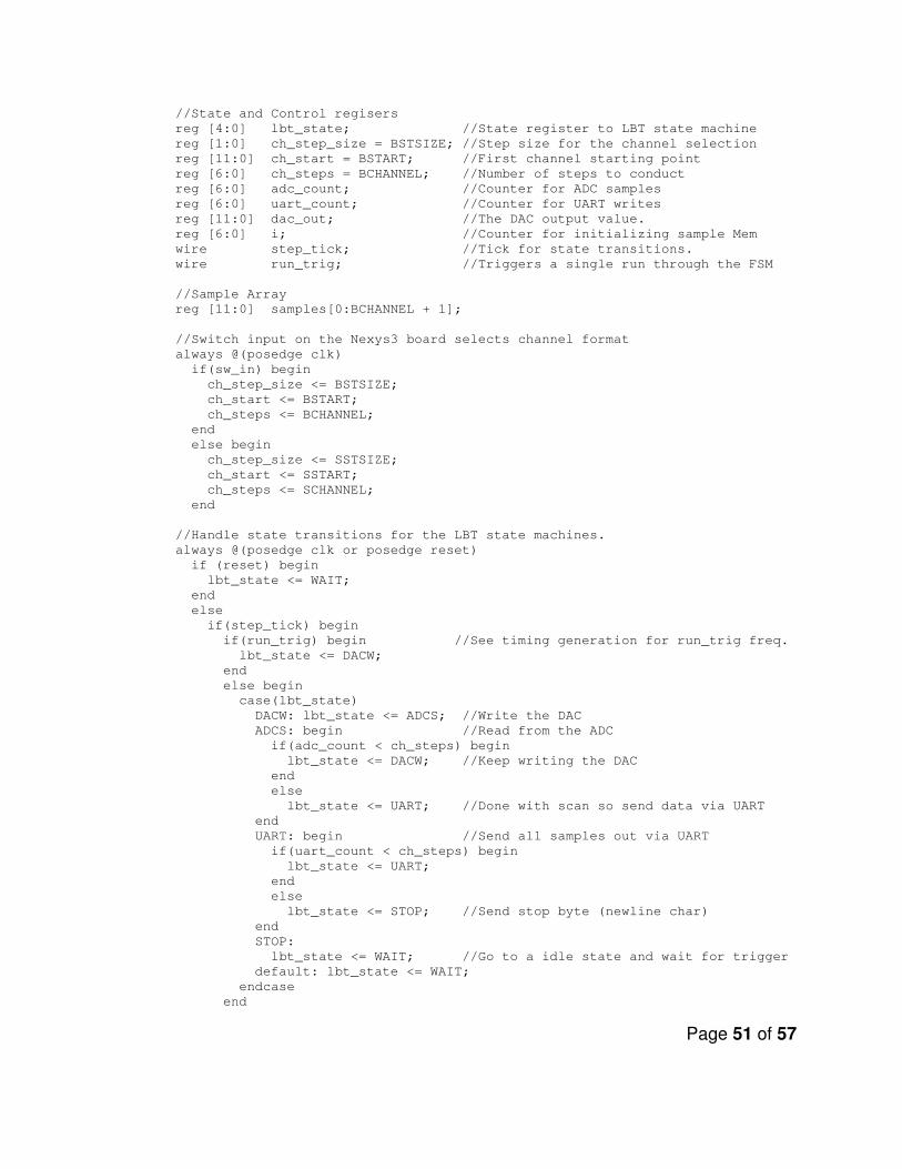
Page 51 of 57
//State and Control regisers
reg [4:0] lbt_state; //State register to LBT state machine
reg [1:0] ch_step_size = BSTSIZE; //Step size for the channel selection
reg [11:0] ch_start = BSTART; //First channel starting point
reg [6:0] ch_steps = BCHANNEL; //Number of steps to conduct
reg [6:0] adc_count; //Counter for ADC samples
reg [6:0] uart_count; //Counter for UART writes
reg [11:0] dac_out; //The DAC output value.
reg [6:0] i; //Counter for initializing sample Mem
wire step_tick; //Tick for state transitions.
wire run_trig; //Triggers a single run through the FSM
//Sample Array
reg [11:0] samples[0:BCHANNEL + 1];
//Switch input on the Nexys3 board selects channel format
always @(posedge clk)
if(sw_in) begin
ch_step_size <= BSTSIZE;
ch_start <= BSTART;
ch_steps <= BCHANNEL;
end
else begin
ch_step_size <= SSTSIZE;
ch_start <= SSTART;
ch_steps <= SCHANNEL;
end
//Handle state transitions for the LBT state machines.
always @(posedge clk or posedge reset)
if (reset) begin
lbt_state <= WAIT;
end
else
if(step_tick) begin
if(run_trig) begin //See timing generation for run_trig freq.
lbt_state <= DACW;
end
else begin
case(lbt_state)
DACW: lbt_state <= ADCS; //Write the DAC
ADCS: begin //Read from the ADC
if(adc_count < ch_steps) begin
lbt_state <= DACW; //Keep writing the DAC
end
else
lbt_state <= UART; //Done with scan so send data via UART
end
UART: begin //Send all samples out via UART
if(uart_count < ch_steps) begin
lbt_state <= UART;
end
else
lbt_state <= STOP; //Send stop byte (newline char)
end
STOP:
lbt_state <= WAIT; //Go to a idle state and wait for trigger
default: lbt_state <= WAIT;
endcase
end

Page 52 of 57
end
//Handle state machine outputs
always @(posedge clk or posedge reset)
if (reset) begin
adc_trig <= 1'b0;
dac_trig <= 1'b0;
uart_trig <= 1'b0;
dac_out <= BSTART;
uart_data <= 8'd0;
adc_count <= 6'd0;
uart_count <= 6'd0;
//Initialize the sample buffer to all 0's
for (i = 1'd0; i < BSTART; i = i + 1'd1) begin
samples[i] <= 12'd0;
end
end
else begin
//See timing generation for tick values below
if(step_tick) begin
case(lbt_state)
WAIT: begin
dac_trig <= 1'b0;
adc_trig <= 1'b0;
uart_trig <= 1'b0;
dac_out <= ch_start;
adc_count <= 6'd0;
uart_count <= 6'd0;
end
DACW: begin //Write the new value for the DAC and trigger DAC module
dac_trig <= 1'b1;
dac_out <= dac_value + ch_step_size;
end
ADCS: begin //Read the sampled power level with the ADC
adc_trig <= 1'b1;
adc_count <= adc_count + 1'd1;
samples[adc_count] <= adc_data[11:0];
end
UART: begin //Send sample buffer out via UART
uart_trig <= 1'b1;
//Scale up the data to avoid the PC side getting confused about a
//hex code of 10 (newline character).
uart_data <= samples[uart_count][6:0] + 4'd15;
uart_count <= uart_count + 1'd1;
end
STOP: begin //Send the UART newline character (0x0D).
uart_trig <= 1'b1;
uart_data <= 8'd10;
//Reset the DAC value back to the first channel
dac_trig <= 1'b1;
dac_out <= ch_start;
end
default: begin
adc_trig <= 1'b0;
dac_trig <= 1'b0;
uart_trig <= 1'b0;
end
endcase
end
else begin

Page 53 of 57
dac_trig <= 1'b0;
adc_trig <= 1'b0;
uart_trig <= 1'b0;
end
end
assign dac_value = dac_out;
//****************************************************************************/
// Timing Generation
//****************************************************************************/
//Clock enable divider
localparam hz_5k = 16'd39_999; //Actually 2500Hz
//Counter Registers
reg [15:0] ck_count_5k = 0;
reg tick5khz = 0;
// Generate 5kHz pulse
always @(posedge clk)
if (ck_count_5k == hz_5k) begin
ck_count_5k <= 0;
tick5khz <= 1'b1;
//tick5khz <= ~tick5khz;
end
else begin
ck_count_5k <= ck_count_5k + 1'b1;
tick5khz <= 1'b0;
end
//Clock enable dividers
localparam hz_20 = 26'd49_999_999; // TRUE 20Hz
//Counter Registers
reg [25:0] ck_count_20 = 0;
reg tick20hz = 0;
// Generate 20Hz pulse
always @(posedge clk)
if (ck_count_20 == hz_20) begin
ck_count_20 <= 0;
tick20hz <= 1'b1;
end
else begin
ck_count_20 <= ck_count_20 + 1'b1;
tick20hz <= 1'b0;
end
//Triggers a scan of the channels every 500ms
assign run_trig = tick20hz;
//This is the scanning state machine tick
assign step_tick = tick5khz;
endmodule

Page 54 of 57
Appendix B. Schematics for RF, DAC, and ADC Hardware
Block Diagram
DAC Hardware (Note that only 1 channel was used in this work).

Page 55 of 57
ADC Hardware (Note only one channel was used in this work
Nexys3 Interface connections

Page 56 of 57
VCO and amplifier. Note that the MAX2634 amplifier was replaced with the Avago
amplifier circuit shown below due to the MAX2634 having too low a compression point.
Avago power amplifier for boosting the VCO output to around +7dBm.

Page 57 of 57
Mixer, IF diplex filter and Diode detector circuit. Note that the HSMS-2850 was replaced
with a Skyworks zero-biased Schottky detector diode.