author : fabrice bernard-granger september 18th, … · mtj resistive states ... semiconductor...
TRANSCRIPT

Author : Fabrice BERNARD-GRANGER
September 18th, 2014

Fabrice BERNARD-GRANGER
September, 18th 2014 Keysight Semiconductor Devices Characterisation Seminar 2
Spintronic Introduction
Spintronic Design Flow and Compact Modelling
Process Variation and Design Impact

Fabrice BERNARD-GRANGER
September, 18th 2014 Keysight Semiconductor Devices Characterisation Seminar 3
Spintronic Introduction
Spintronic Design Flow and Compact Modelling
Process Variation and Design Impact

Fabrice BERNARD-GRANGER
September, 18th 2014 Keysight Semiconductor Devices Characterisation Seminar 4
Electronic Spintronic
information is conveyed using electron charge (e-) . Generation, manipulation, detection of charge currents: flow of electrons The most used material is semiconductor (Si)
information is conveyed through electron spin (e↓ or e↑). Generation, manipulation, detection of spin currents: flow of magnetic moments. The material of choice is ferromagnetic alloy (Fe, Co, Mg)
M magnetization vector of a ferromagnetic layer
50% e↑
50% e↓ electron
flux
with X << Y
Electron flux
spin polarized
Albert Fert, French physicist, was awarded the 2007 Nobel Prize
Magneto resistance
effect in multi
layer stack
Spin polarized current
Electron spin
Current I
Y% e↑
X% e↓

Fabrice BERNARD-GRANGER
September, 18th 2014 Keysight Semiconductor Devices Characterisation Seminar 5
A Magnetic Tunnel Junction
is the basic device used for storing information in a MRAM
Free layer
Reference Layer
r low resistance R large resistance
R r
AP state = 1 P state = 0
Oxide layer
MTJ stack
Free layer magnetization dynamic
during writing process
MTJ resistive states
M magnetization vector of a ferromagnetic layer

Fabrice BERNARD-GRANGER
September, 18th 2014 Keysight Semiconductor Devices Characterisation Seminar 6
Use electron spin added
to its electric charge
Standalone MRAM,
TMR (early 00’s)
HDD, GMR
(early 80’s)
Embedded MRAM &
Distribute non-volatility
within logic
(development)
Field Induce
Magnetic Switching
(FIMS, Toggle)
Thermally
Assisted Switching
(TAS)
Spin Torque
Transfer
(STT)
Spin-Based
Logic ?
…Spin Orbit
Torque
(SOT)

Fabrice BERNARD-GRANGER
September, 18th 2014 Keysight Semiconductor Devices Characterisation Seminar 7
MRAM an emergent and credible candidate for SRAM and flash replacement

Fabrice BERNARD-GRANGER
September, 18th 2014 Keysight Semiconductor Devices Characterisation Seminar 8
Q3, 2014
Altera has taken the lead in enabling ST-MRAM within memory and storage markets supported by high performance, low power FPGAs
20 Japanese & US Cies joined their efforts on MRAM development Q4, 2013

Fabrice BERNARD-GRANGER
September, 18th 2014 Keysight Semiconductor Devices Characterisation Seminar 9
XMC a Chineese foundry, plan to developp MRAM process in 2015 http://www.xmcwh.com/technology/process-technology/
Q1, 2014
Q3, 2014
The mobile chip giant Qualcomm has also been working on STT-MRAM, and in a recent test of TDK-Headway’s chips, it found no errors in data retention after 528 hours at 150 °C.

Fabrice BERNARD-GRANGER
September, 18th 2014 Keysight Semiconductor Devices Characterisation Seminar 10
Spintronic Introduction
Spintronic Design Flow and
Compact Modelling
Process Variation and Design Impact
Fabrice BERNARD-GRANGER
September, 18th 2014 Keysight Semiconductor Devices Characterisation Seminar 11
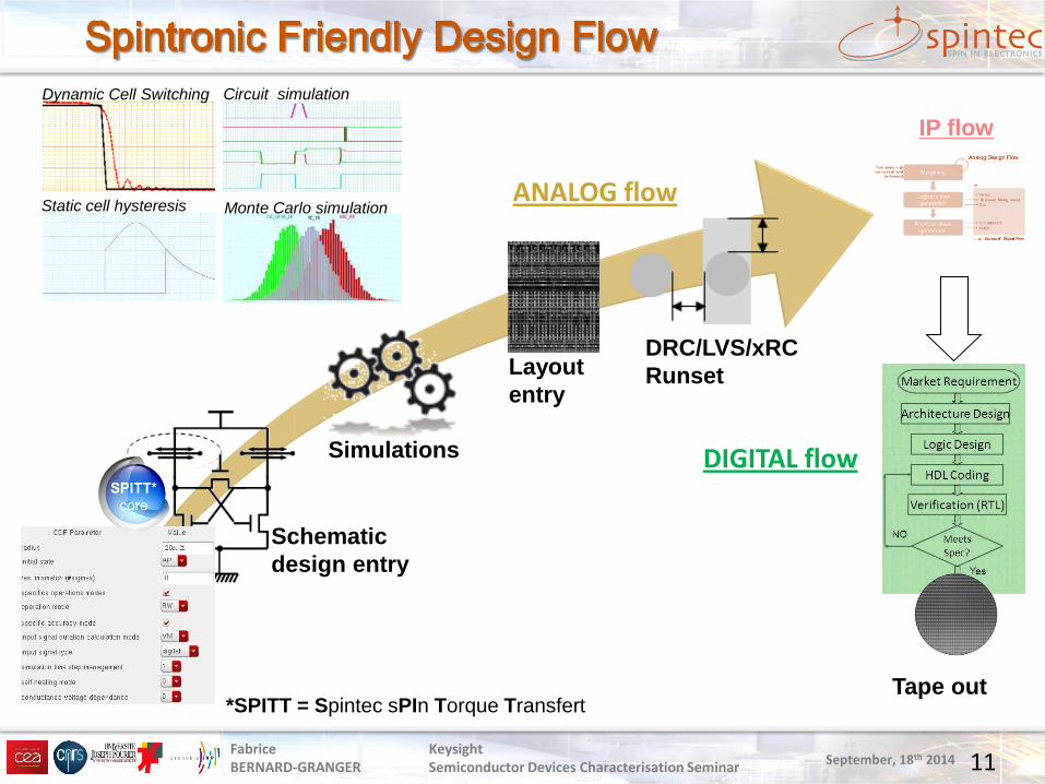
Schematic
design entry
Simulations
Layout
entry
DRC/LVS/xRC
Runset
Tape out
IP flow
Monte Carlo simulation
Dynamic Cell Switching
Static cell hysteresis
Circuit simulation
*SPITT = Spintec sPIn Torque Transfert
ANALOG flow
DIGITAL flow

Fabrice BERNARD-GRANGER
September, 18th 2014 Keysight Semiconductor Devices Characterisation Seminar 12
SPITT*
core
Extraction/fit module (in progress with LETI) Dedicated fitting algorithm
ICCAP tool plugin
Physics
TCAD
SPICE model SPITT
(Spintec sPIn Torque Transfert)
Modes (accuracy vs. speed)
Physical phenomenon
SPICE
simulator
STTRAM
Raw data Model card
parameters
corners and statistic

Fabrice BERNARD-GRANGER
September, 18th 2014 Keysight Semiconductor Devices Characterisation Seminar 13
State - V I-V R-V
SPITT Model
Merits figures

Fabrice BERNARD-GRANGER
September, 18th 2014 Keysight Semiconductor Devices Characterisation Seminar 14
Spintronic Introduction
Spintronic Design Flow and Compact Modelling
Process Variation and Design
Impact

Fabrice BERNARD-GRANGER
September, 18th 2014 Keysight Semiconductor Devices Characterisation Seminar 15
5 corners set to catch process variation in a MTJ based on
the following parameters:
• RA (sheet resistance) [Ω.um²] (+/- 3 σ*)
• TMR (Tunneling Mangeto Resistance = ∆R/R) [%] (+/- 3 σ*)
• ISW (Switching Current) [uA] (+/- 3 σ*)
SWITCHING CURRENT
RESISTANCE
* σ = Gaussian distribution width

Fabrice BERNARD-GRANGER
September, 18th 2014 Keysight Semiconductor Devices Characterisation Seminar 16
Reduction to speed up the development phase
3 T
25 P 3 V
Full MRAM = MRAM Cell + all CMOS logic / analogic
MRAM Cell = MTJ + Nmos transistor
# MRAM Process corners = 25
= 5 MTJ corners * 5 MOS corners
P
V
T
# MRAM Voltage corners = 3
Vdd –x%, Vdd, Vdd +x%
# MRAM Temprature corners = 3
Tmin, 27°C, Tmax
225 corners

Fabrice BERNARD-GRANGER
September, 18th 2014 Keysight Semiconductor Devices Characterisation Seminar 17
5 functionals architectures @ nominal conditions
225 corners
around 10 times less
Electrical simulations across all PVT
σMTJ large σMTJ small
Design functionality loss due to inaccurate MTJ characterization

Fabrice BERNARD-GRANGER
September, 18th 2014 Keysight Semiconductor Devices Characterisation Seminar 18
Logic
Arithmetic Logic Unit Standard cell library (latch, flip flop, register..) Nano processor (based on spintronics cells)
FPGA
Look Up Table (silicon proven)
Memory, IC Design
Test chip circuit (test device oriented) STT-RAM Full 256kb, 1 Mb and 4Mb single port compiler oriented (design on going) 8x8b SOT-RAM + peripheries (tape out ongoing)
Standard Cell
Circuit
Memory
• Fabless
• Design analog-numeric-system
• Control processors data centric

Fabrice BERNARD-GRANGER
September, 18th 2014 Keysight Semiconductor Devices Characterisation Seminar 19
Spintronic technology
Non volatility key for power reduction
Ready for MRAM production
New technology = new flow to set-up
Silicon characterization
PDK and Full Design plateform developement
Spintronic impact @ system level
Architecture tremendously modified
New functionality arising
