audio-triggered el wire sequencer
TRANSCRIPT
Audio-Triggered EL Wire Sequencer
by
Ben Paik
Senior Project
Electrical Engineering Department
California Polytechnic State University
San Luis Obispo
June, 2011

i
Table of Contents
Section Page List of Tables and Figures ii Acknowledgements iv Abstract v
I. Introduction 1
II. Background 2
III. Requirements 4
IV. Design 7
V. Test Plans 14
VI. Development and Construction 17
VII. Integration and Test Results 19
VIII. Conclusion 29
IX. Bibliography 30 Appendices A. Specifications/Requirements 31 B. Parts List/Costs 34 C. Schedule/Time Estimates 35
D. PCB Layout 37
E. Program Listing 38
F. Hardware Configuration/Layout 56
ii
List of Tables and Figures
Table Page Table I: Frequency Response of MSGEQ7 24 Table II: MSGEQ7 Filter Characteristics 26 Table III: Parts List and Costs 34 Figure Figure 1: System Design Block Diagram 7 Figure 2: Sequencer Design 9
Figure 3: Optoisolator TRIAC 10
Figure 4: ATMega32A Pin Diagram 11
Figure 5: Audio Amplifier Circuit Schematic 12
Figure 6: MSGEQ7 Wiring Diagram 13
Figure 7: Single Unit in EL Wire Sequencer 14
Figure 8: PCB Layout for Sequencer 18
Figure 9: Modified PCB Connection 20
Figure 10: TRIAC Diagram 20
Figure 11: Frequency Response of MSGEQ7 (full range) 23
Figure 12: Frequency Response of MSGEQ7 (lower frequencies)
24
Figure 13: Software Block Diagram 27 Figure 14: Revised System Block Diagram 28 Figure 15: Project Schedule 35

iii
Figure 16: PCB Layout 36 Figure 17: Final System Block Diagram 56

iv
Acknowledgements
This project was made possible by the contributions of Dr. John Oliver and Paul Saueressig.
My senior project advisor, Dr. John Oliver was tremendously helpful in planning out my
approach, keeping me on schedule, and as a consultant through various aspects of the
project’s development. My neighbor, Paul Saueressig, was also incredibly helpful in the
design and construction of the housing for the EL wire. Without the benefit of his expertise
and machine shop, this would have been virtually impossible.
v
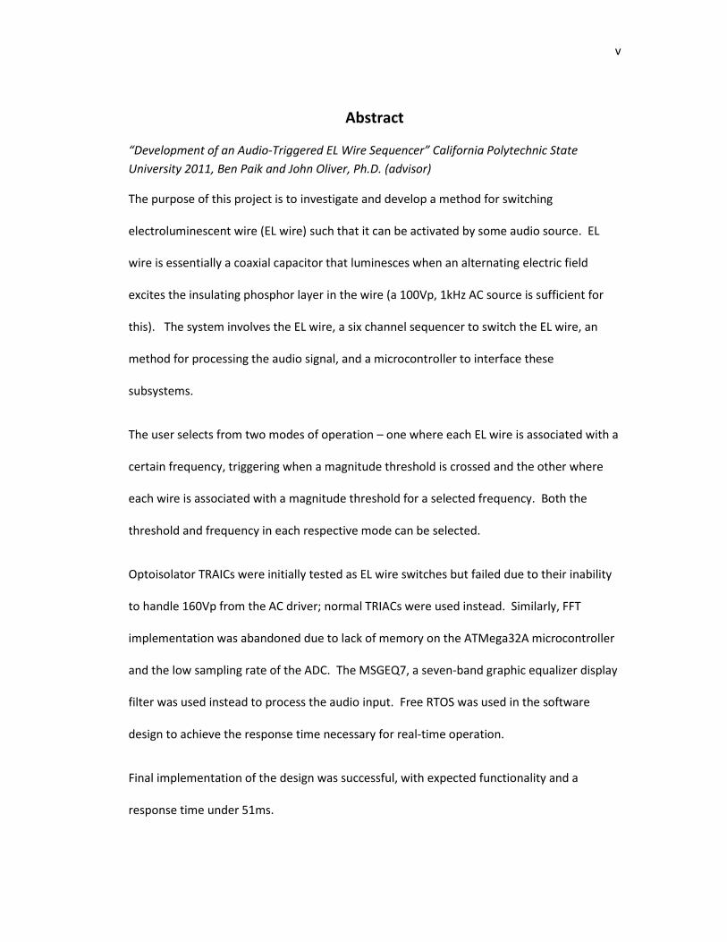
Abstract
“Development of an Audio-Triggered EL Wire Sequencer” California Polytechnic State
University 2011, Ben Paik and John Oliver, Ph.D. (advisor)
The purpose of this project is to investigate and develop a method for switching
electroluminescent wire (EL wire) such that it can be activated by some audio source. EL
wire is essentially a coaxial capacitor that luminesces when an alternating electric field
excites the insulating phosphor layer in the wire (a 100Vp, 1kHz AC source is sufficient for
this). The system involves the EL wire, a six channel sequencer to switch the EL wire, an
method for processing the audio signal, and a microcontroller to interface these
subsystems.
The user selects from two modes of operation – one where each EL wire is associated with a
certain frequency, triggering when a magnitude threshold is crossed and the other where
each wire is associated with a magnitude threshold for a selected frequency. Both the
threshold and frequency in each respective mode can be selected.
Optoisolator TRAICs were initially tested as EL wire switches but failed due to their inability
to handle 160Vp from the AC driver; normal TRIACs were used instead. Similarly, FFT
implementation was abandoned due to lack of memory on the ATMega32A microcontroller
and the low sampling rate of the ADC. The MSGEQ7, a seven-band graphic equalizer display
filter was used instead to process the audio input. Free RTOS was used in the software
design to achieve the response time necessary for real-time operation.
Final implementation of the design was successful, with expected functionality and a
response time under 51ms.
1
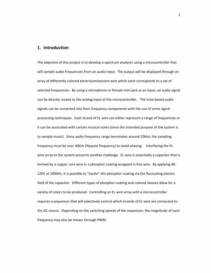
1. Introduction
The objective of this project is to develop a spectrum analyzer using a microcontroller that
will sample audio frequencies from an audio input. The output will be displayed through an
array of differently colored electroluminescent wire which each corresponds to a set of
selected frequencies. By using a microphone or female mini-jack as an input, an audio signal
can be directly routed to the analog input of the microcontroller. The time-based audio
signals can be converted into their frequency components with the use of some signal
processing techniques. Each strand of EL wire can either represent a range of frequencies or
it can be associated with certain musical notes (since the intended purpose of the system is
to sample music). Since audio frequency range terminates around 20kHz, the sampling
frequency must be over 40kHz (Nyquist frequency) to avoid aliasing. Interfacing the EL
wire array to the system presents another challenge. EL wire is essentially a capacitor that is
formed by a copper core wire in a phosphor coating wrapped in fine wire. By applying 90-
120V at 1000Hz, it is possible to “excite” this phosphor coating via the fluctuating electric
field of the capacitor. Different types of phosphor coating and colored sleeves allow for a
variety of colors to be produced. Controlling an EL wire array with a microcontroller
requires a sequencer that will selectively control which strands of EL wire are connected to
the AC source. Depending on the switching speeds of the sequencer, the magnitude of each
frequency may also be shown through PWM.

2
II. Background
Electroluminescence is a phenomenon by which a material will emit light (or luminesces)
when an electrical current or field is applied to it. The electric current or field raises the
electrons in the material to a higher energy state and drop back to their original energy
levels – emitting photons in the process. This has been adapted to suit a wide variety of
applications such as LEDs and LCD display backlights. LEDs are a common example of
electroluminescence via electric current while the LCD display backlights demonstrate
electroluminescence via electric field. Generally speaking, electric field-based
electroluminescence will have diffused appearance than its current-based counterpart.
Phosphor powder is typically used as the electroluminescent medium in electric field
electroluminescence. The phosphor acts as the insulating layer between the plates of a
capacitor which generate the required electric field when powered by an AC source. 100Vp
or greater is typically required for luminescence with higher voltages producing greater
luminosity. Similarly, frequency can vary from around 60Hz to several kilohertz with higher
frequencies producing greater luminosity (though higher frequencies reduce the lifetime of
the medium). Electroluminescence produced in this manner is unique in that it is completely
non-directional (i.e. perfectly homogeneous) which is the cause of its diffused appearance.
[1], [2]
Electroluminescent wire (EL wire) is a fairly recent implementation of electric field-based
electroluminescence. Developed in 1998 by ELAM EL Industries, Ltd. (LyTec), EL wire uses
3
coaxial capacitance to create electroluminescence in a wire rather than a flat surface. It
consists of a copper wire core insulated by the phosphor coating. Another copper wire is
wound around the phosphor to create the coaxial capacitor between the two conductors.
100Vp AC at 1kHz tends to be the standard operating range for most EL wire. EL wire is
currently being used in a variety of applications due to its low cost, low power, and
flexibility. Though it is being used as a substitute for neon signs, its greatest market resides
with hobbyists who use it to accentuate their projects (such as costumes or art pieces).
[3], [4]

4
III. Requirements - this section discusses the desired performance of the system. It details the user
interface, the system/subsystem specifications.
A. User Controls
1. Button 1:
Upon startup, the system will be in MODE 1. Pressing button 1 will toggle the mode of the
system between MODE 1 and MODE 2.
2. Button 2:
In MODE 1, this button acts as a sensitivity control for triggering the EL wire. It increments
the threshold level by 100 each time it is pressed (the threshold is scaled to the 10-bit ADC
for a minimum threshold of 100 and a maximum threshold of 1000). The threshold defaults
to 100 on startup and each time MODE 1 is reentered. In MODE 2, this button increments
the frequency whose magnitude will be represented on the EL wire. The lowest frequency is
the default value for upon entering MODE 2.
B. Specifications
1. System:
- The system will receive an audio signal via standard 3.5mm TRS connector (i.e. minijack)
that will serve as the input to the system. This was chosen over a microphone input to
eliminate external noise and preserve the bandwidth of the audio (since many
microphones only have a 10kHz range).
- The system shall operate in two modes which can be selected with a mode button.
5
- The output of the system shall consist of six strands of differently colored EL wire, each
with common threshold and unique frequency band (MODE 1).
- The output of the system shall consist of six strands of differently colored EL wire which
all have a unique threshold and share a frequency selected by a frequency button
(MODE 2). The frequency defaults to the lowest frequency once the mode is entered
and is incremented up as the frequency button is pressed (the frequency rolls over to
the lowest frequency after the highest frequency is selected).
- The system shall consist of three main subsystems that allow it to operate properly: the
sequencer, the spectrum analyzer, and the software.
2. Subsystems:
Sequencer:
- The sequencer will interface between the six strands of EL wire, the AC source, and the
microcontroller.
- The sequencer will have seven lines that connect to the microcontroller port. These
include a common ground and six control lines that can route the corresponding EL wire
to the AC source when a 5V signal is applied to the input pin.
- The 5V input signal should be current limited to under 20mA so that in can be sourced
by the microcontroller.
- The 5V input signal should be current limited to under 20mA so that in can be sourced
by the microcontroller.
- The control lines shall all be active HIGH.

6
Spectrum Analyzer:
- The spectrum analyzer shall produce a minimum of six frequency bands – one for each
strand of EL wire (For FFT implementation, this corresponds to a minimum length of
N=8.)
- The spectrum analyzer shall span frequencies within the audible range (<20kHz) with a
maximum frequency of at least 16kHz.
- According to the sampling theorem, the sample rate of the spectrum analyzer must be
at least 32kHz in order to recover the 16kHz maximum frequency.
Software:
- The software must handle the operation of all subsystems in real time (this means
running the spectrum analyzer and updating to the EL wire sequencer in under 50ms
every cycle).
- The software must also implement the user interface. This means handling the mode
switching, threshold switching (in MODE 1), frequency switching (in MODE 2), and
button debouncing.
7
IV. Design
- This section gives an overview of the initial design on the system level and more
specifically on the subsystem level.
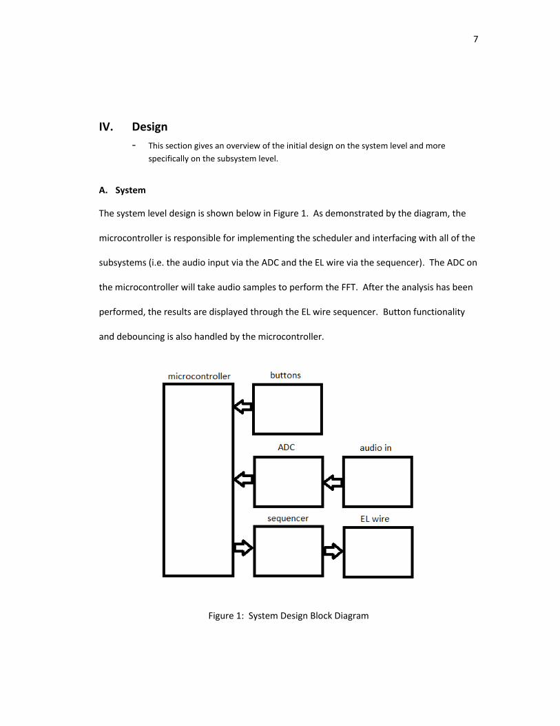
A. System
The system level design is shown below in Figure 1. As demonstrated by the diagram, the
microcontroller is responsible for implementing the scheduler and interfacing with all of the
subsystems (i.e. the audio input via the ADC and the EL wire via the sequencer). The ADC on
the microcontroller will take audio samples to perform the FFT. After the analysis has been
performed, the results are displayed through the EL wire sequencer. Button functionality
and debouncing is also handled by the microcontroller.
Figure 1: System Design Block Diagram

8
B. Subsystems
1. Sequencer:
The circuit schematic for the EL wire sequencer is shown below in Figure, 2 where each
strand of EL wire is represented by a capacitor (since EL wire is effectively modeled as a
coaxial capacitor). The sequencer can be broken down into six identical units (one for each
strand of EL wire) connected in parallel with the driver (160Vp at 4.6kHz AC source). Each
unit consists of an EL wire strand in series with a TRIAC [5], which acts as a switch for the AC
source. A 1k Ohm resistor is used to limit the current at the gate of the TRIAC to under
20mA (the maximum current the microcontroller can source). Activating multiple TRIACS
simultaneously has the effect of adding capacitors in parallel to the source (or lengthening
the EL wire). Additionally, there is a ceramic capacitor placed in parallel with the AC source
to protect the AC driver (which cautions against using the driver with no EL wire attached).
This way the driver will always have a load to supply, even if none of the TRIACS are
activated.

9
Figure 2: Sequencer Design
A similar sequencer design can also be implemented using optoisolator TRIACs [6] which
would serve to protect the microcontroller from the AC source. In this design, the
microcontroller pins and the EL wire are electrically independent from each other. This is
accomplished by having a photosensitive TRIAC connected to the EL wire and AC source
while an internal LED is connected to the microcontroller pins. The unit for this design is
shown below in Figure 3.
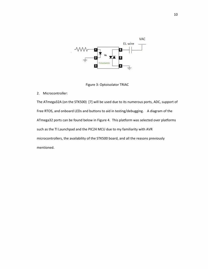
10
Figure 3: Optoisolator TRIAC
2. Microcontroller:
The ATmega32A (on the STK500) [7] will be used due to its numerous ports, ADC, support of
Free RTOS, and onboard LEDs and buttons to aid in testing/debugging. A diagram of the
ATmega32 ports can be found below in Figure 4. This platform was selected over platforms
such as the TI Launchpad and the PIC24 MCU due to my familiarity with AVR
microcontrollers, the availability of the STK500 board, and all the reasons previously
mentioned.

11
Figure 4: ATMega32A Pin Diagram
3. Spectrum Analyzer:
The Spectrum Analyzer will be implemented with on the microcontroller using the 10-bit
ADC [7] to obtain samples required for the FFT. The audio will be input to the ADC through
an inverting amplifier (shown below in Figure 5 [8]), designed to provide the DC offset
necessary to ensure that the input to the ADC is always positive. The FFT algorithm will be
64 points to improve the speed of the calculation.

12
Figure 5: Audio Amplifier Circuit Schematic
If an FFT is not feasible in this system, a graphic equalizer display filter will be used to
perform the frequency instead. The MSGEQ7 [9] is such an IC configured as a multiplexed
array of seven bandpass filter and peak detectors. The frequencies and corresponding
magnitudes are accessed sequentially (63 Hz, 160 Hz, 400 Hz, 1 kHz, 2.5 kHz, 6.25 kHz, 6.25
kHz, and 16kHz) via a strobe line. The magnitude of the currently selected frequency is
output as a DC voltage from 0 to 5V. Thus the IC can be seamlessly interfaced with the
microcontroller by toggling the strobe line with a standard digital out and reading the
resulting DC voltage through the ADC. A wiring diagram of the MSGEQ7 is shown below in
Figure 6.

13
Figure 6: MSGEQ7 Wiring Diagram
4. Software:
The software is to be implemented using Free RTOS [10]. Tasks will be made to obtain
samples from the ADC, perform the FFT, output to the EL wire, change modes, and handle
button debouncing.

14
V. Test Plans
- This section details the methods by which all the components in the system will be
tested and evaluated.
A. EL Wire:
EL wire will be characterized by measuring its current consumption, capacitance, and
luminosity as a function of frequency/voltage.
B. Sequencer:
Primary testing for the sequencer involves testing the TRIACs and optoisolator TRIACs to
switch EL wire. This will be done by testing individual the units of each sequencer. The
switching characteristics of each mechanism can be determined by applying a 5V square
wave with 2.5V DC offset to the inputs of each unit (shown below in Figure 7 for the TRIAC
and previously in Figure 3 for the optoisolator version) and varying the frequency. The
maximum switching speed of the TRIACs and optoisolators can be determined in this way.
Figure 7: Single Unit in EL Wire Sequencer

15
C. ADC:
Once properly configured in the microcontroller, the accuracy of the ADC can be tested with
a DC power supply and 4-digit seven segment display [11] interfaced to the SPI port of the
microcontroller. Since the ADC has 10-bit resolution, the full range (0 to 1024) of the ADC
can be shown on the seven segment display, and its accuracy can be determined by
comparing this to the multimeter result. Source code for the ADC testing can be found in
the program listing appendix.
D. Audio Amplifier Test:
The audio amplifier simply needs to be built and have the DC offset verified. Gain
bandwidth product is not very important in this case since the maximum frequency that will
be measured is 20kHz and the gain can be as low as unity since the signal from the audio
source (ipod/computer) can surpass the 5V range of the ADC independently (it just needs
the DC offset).
E. FFT Test:
Once completed, the FFT can be tested by sweeping frequencies of constant magnitude
from a function generator on the input of the ADC. The FFT result can be determined by
finding the magnitude of individual frequency bands independently by using the previously
mentioned 7-segment display. For example, inputting a 2.5V 1 kHz sine wave to the ADC
should produce a value near 512 on the seven segment display when selecting for frequency
bands near 1 kHz.
16
F. MSGEQ7:
This IC will be tested by measuring pure sinusoids of 100mVpp in various frequency
increments from 0 to 20 kHz. The resulting DC voltage will be recorded for each of the
seven bands at every input frequency. Frequency increments will be selected to improve
resolution near the center frequencies of each bandpass filter. Measurements will also be
taken to determine the bandwidths of each filter.
G. Software:
The software will be tested incrementally as part of the evaluation of each of the previous
subsystems. Once this is complete, tasks will be created using Free RTOS to manage and
integrate each of the subsystems together. Testing will be done using the onboard LEDs of
the STK500 before interfacing to the sequencer (with the only code modification being
writing vales for the active-LOW LEDs rather than for the active-HIGH sequencer). Once this
functions properly, the sequencer can be interfaced to the system. Proper functionality can
be ensured by applying a 100mVpp sinusoid to the audio input and sweeping the frequency
from 0Hz to 20kHz while observing when each LED is activated.

17
VI. Development and Construction
- This section explains how the major components of the system were developed over the
course of the project. It explains modifications made to existing components as well as
the construction of custom components.
A. EL Wire:
In order to connect to the male Molex headers on the PCB, each of the six EL wire strands
needed to be fitted with the corresponding female headers. This involved cutting the
original connectors on the EL wire, stripping the leads, and soldering them to the leads on
the female Molex headers. These connections were also shrink-wrapped to protect the
solder points.
B. Housing:
The housing for the EL wire display began with a concept sketch that guided the
development and construction process. The array of EL wires would be enclosed in glass
with an internal frame to support an intricate spiral pattern. The entire structure was
custom built from brass tubing and aluminum plates in a machine shop over several days
and eventually came to bare a strong resemblance to the initial concept design.
C. Sequencer:
The sequencer was implemented on a printed circuit board (PCB) designed and ordered
through ExpressPCB. The board was 3.8” x 2.5” and can be seen below in Figure 8. This
board was implemented using the optoisolator TRIAC design shown in Figure 3. The red
traces represent the top layer while the green traces represent the bottom layer of the
board. On the far left is the seven pin Molex connecter used to interface with the
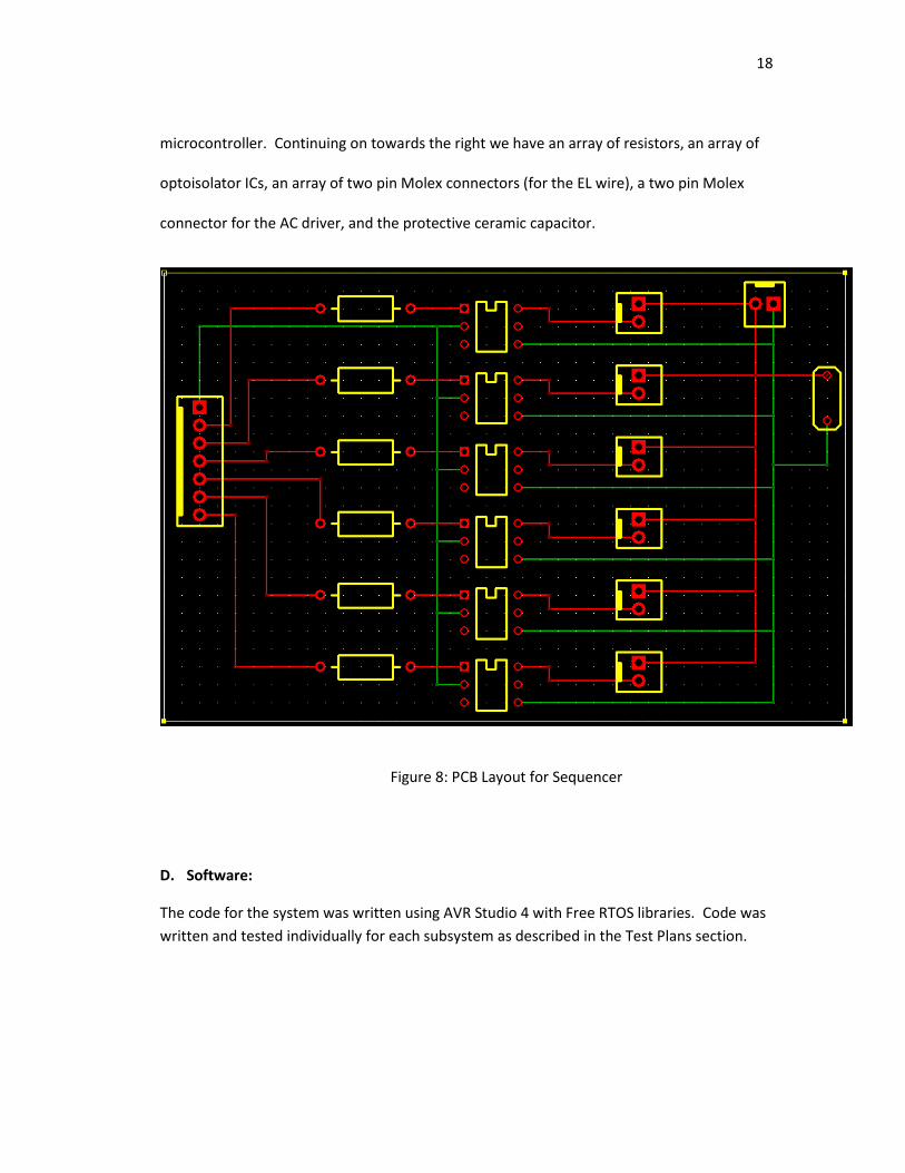
18
microcontroller. Continuing on towards the right we have an array of resistors, an array of
optoisolator ICs, an array of two pin Molex connectors (for the EL wire), a two pin Molex
connector for the AC driver, and the protective ceramic capacitor.
Figure 8: PCB Layout for Sequencer
D. Software:
The code for the system was written using AVR Studio 4 with Free RTOS libraries. Code was
written and tested individually for each subsystem as described in the Test Plans section.
19
VII. Integration and Test Results - This section details the results of all the tests that were previously outlined and what, if
any design modifications needed to be made in response to these tests to implement
the system.
A. EL Wire:
Each of the five foot strands of EL wire had a capacitance of 20nF and drew 15mA. This
came out to 4nF/ft. and 3mA/ft. for the 2mm gauge EL wire used in this project. Since the
light produced by EL wire is non-directional, it was impossible to attain luminosity
measurements as functions of frequency/voltage with lumen meters.
B. Optoisolator TRIACS:
The optoisolator TRIACs did not function as intended as they are only meant for low level
signals. Thus, the 160Vp sinusoid was too large for the optoisolators to handle. When used
in the circuit shown in Figure 3, the optoisolators were able to switch the EL wire on when
5V was placed on the input. However, reducing the input down to 0V did not switch the EL
wire off.
Design Modification:
Due to the results of the optoisolator tests mentioned, the sequencer design from Figure 2
(using standard TRIACs) was selected. Since the PCB shown in Figure 8 had already been
ordered, modifications were made to implement the design from Figure 2 on the PCB. This
simply required wire to be soldered across pins 2 and 4 for all the IC’s drawn on the PCB
(demonstrated below in Figure 9). A1 and A2 (from the TRIAC diagram below in Figure 10)
were soldered onto pins 4 and 6 of Figure 9, and the gate was soldered to pin 1 on Figure 9.

20
Figure 9: Modified PCB Connection
Figure 10: TRIAC Diagram
C. TRIAC:
The basic unit of the EL wire sequencer is shown previously in Figure 7. This unit was tested
with the EL wire driver as the AC source and a 2.5Vp square wave with a 2.5V DC offset as
the input to the 1k Ohm resistor to simulate the digital output from the microcontroller.
The frequency of the square wave was varied to determine the maximum switching
frequency of the TRIACs. The EL wire responded to the input signal until the frequency of
the square wave exceeded 33Hz. At this point, the EL wire simply remained off and did not
luminesce until the frequency dropped below 33Hz.

21
Design Modification:
Since the TRIACs limited the EL wire to a flicker rate well below the desired value (i.e. the
blinking of the EL wire at 33Hz was very apparent), using PWM as a method of representing
magnitude was effectively ruled out. Instead, two distinct modes of operation were
introduced - one showing all measured frequencies simultaneously with low magnitude
resolution and one showing individual frequencies with greater magnitude resolution. This
is explained in depth in the user controls section.
D. ADC:
The accuracy of the ADC was measured in 0.1V increments from 0V to 5V – thus covering
the full ADC range. Each of the 50 voltages that were tested was compared to the 10-bit
ADC result on the four digit seven-segment display. None of these values (on the seven-
segment display) deviated by more than 2 when compared to the voltage measurement on
the multimeter (converted to a 10-bit value with 5V being the full scale range).
While configuring the ADC for free running mode, it was discovered that the maximum
sample rate that could be achieved was 9.615 kHz. This is because the ADC clock frequency
needed to be prescaled within the range of 50 to 200 kHz. Using the internal oscillator for
the microcontroller and the available prescaler selections, the maximum ADC clock
frequency that can be attained within the given range is 125 kHz. Additionally, each ADC
conversion takes 13 clock cycles which means that the sampling frequency is 125 kHz/13 (or
9.615 kHz). When considering the sampling theorem, this means that the maximum
frequency that can be recovered through the FFT is half of the sample rate - 4.807 kHz. This
value is far below the desired 20 kHz maximum frequency to cover the audible range.

22
E. FFT:
Since high frequency resolution was not required for this project, the smallest FFT (low N)
that could be found for AVR microcontrollers seemed the optimal choice. This ended up
being a 64-point FFT written in assembly. However, attempts to implement this failed due
to memory overflows as a result of running Free RTOS on the microcontroller.
Design Modification:
Performing frequency analysis through the FFT was abandoned due to the limitations of the
microcontroller’s sampling rate and memory. Frequency analysis will instead be
implemented using the MSGEQ7, a graphic equalizer display filter IC. As a result of the
design modification, the audio amplifier will no longer be required to provide a DC offset
since the output of the MSGEQ7 is always a positive DC voltage.
F. MSGEQ7:
Test results for the MSGEQ7 are shown in Figure 11 with the corresponding source data in
Table I below. Table I shows all the tested frequencies in the leftmost column and the
corresponding DC outputs (in volts) for each of the seven bandpass filters in the subsequent
columns. The frequency response of each bandpass filter can be seen Figure 11, where each
color is representative of a single bandpass filter as designated in the associated legend. All
input signals had a magnitude of 100mVpp and the only variable parameter was the
frequency. The range of test frequencies spans from 0Hz to 20kHz. The magnitude of the
frequency response is represented by the DC output of the MSGEQ7 which can range from
0V to 5V. Figure 12 is a graph of the same data in Figure 11, but it instead focuses on the
lower frequencies (0Hz to 1.1kHz to better characterize the bandpass filters in that range.

23
As made evident by the graphs in Figures 11 and 12, the peak DC outputs for each bandpass
filter are not identical. The smallest peak is 2.969V for the 400Hz bandpass filter and the
largest peak is 3.797V for the 16kHz bandpass filter. The implication of this is that the
bandpass filters with greater peaks will trigger their corresponding EL wires more easily than
those with smaller peaks, though the 16kHz bandpass is the only filter that really stands out.
It is also noteworthy to mention that the center frequencies for a few of the bandpass filters
on the chip differ significantly from their listed values. Lastly, there is a noticeable
asymmetry in several of the frequency responses (i.e. subsequent peaks), though this should
be of no consequence.
Extra data points were taken near peaks of each bandpass filter to determine the filter
characteristics. Each filter’s peak, 3dB point, actual center frequency, cutoff frequencies,
and bandwidth were determined from the data in Table I and are listed below in Table II.
Figure 11: Frequency Response of MSGEQ7 (full range)
0
0.5
1
1.5
2
2.5
3
3.5
4
0 5000 10000 15000 20000
volt
age
(V
)
frequency (Hz)
63Hz
160Hz
400Hz
1kHz
2.5kHz
6.25kHz
16kHz

24
Figure 12: Frequency Response of MSGEQ7 (lower frequencies)
frequency (Hz) 63Hz 160Hz 400Hz 1kHz 2.5kHz 6.25kHz 16kHz
20 0.4031 0.3094 0.3642 0.3125 0.2812 0.5938 0.3125
50 1.497 0.3406 0.2469 0.2938 0.2 0.2625 0.2625
54 2.094 0.3438 0.2812 0.2812 0.1875 0.3125 0.25
60 3.047 0.3594 0.2969 0.2812 0.1875 0.3125 0.25
63 2.609 0.3906 0.3125 0.2969 0.2031 0.3281 0.2656
66 2.078 0.4062 0.2969 0.2969 0.1875 0.3125 0.25
70 1.609 0.4531 0.3281 0.2344 0.3594 0.2656 0.2969
100 0.7156 0.6375 0.3875 0.325 0.2 0.325 0.2871
141 0.5 2.094 0.4219 0.3281 0.2031 0.3215 0.2656
155 0.4688 2.969 0.4531 0.3281 0.2188 0.3281 0.2656
169 0.4531 2.094 0.5 0.3438 0.2344 0.3281 0.2656
160 0.4812 2.747 0.4812 0.3406 0.1844 0.3406 0.2781
200 0.3719 1.044 0.6062 0.3406 0.2312 0.3406 0.2625
300 0.3719 0.5125 1.294 0.4656 0.2625 0.3719 0.45
340 0.3438 0.4531 2.219 0.4688 0.2812 0.3438 0.2812
370 0.3594 0.4219 3.125 0.5 0.2812 0.3438 0.2812
408 0.3594 0.3906 2.203 0.5469 0.2969 0.3438 0.2969
400 0.3406 0.3875 2.466 0.5437 0.3094 0.3406 0.2781
0
0.5
1
1.5
2
2.5
3
3.5
0 200 400 600 800 1000 1200
volt
age
(V
)
frequency (Hz)
Series1
Series2
Series3
Series4

25
500 0.2469 0.325 1.028 0.6531 0.3094 0.3562 0.2938
800 0.2969 0.2656 0.5469 1.828 0.4219 0.4219 0.3281
829 0.3125 0.2656 0.5156 2.219 0.4062 0.4062 0.3125
900 0.3125 0.2656 0.4844 3.141 0.4375 0.4219 0.3125
1000 0.2938 0.2469 0.4344 2.216 0.4656 0.3875 0.3094
1050 0.2969 0.2969 0.4219 1.797 0.5469 0.4219 0.2969
1100 0.2969 0.2656 0.4219 1.453 0.5156 0.4219 0.2969
1200 0.2969 0.2344 0.4219 1.078 0.5781 0.4219 0.3094
1500 0.3094 0.2156 0.3406 0.7625 0.8094 0.4031 0.3094
1750 0.2781 0.2156 0.3406 0.6219 1.138 0.4969 0.3406
2000 0.2781 0.2 0.3406 0.5437 1.95 0.5125 0.3406
2200 0.2781 0.2156 0.3406 0.5281 3.016 0.6094 0.3594
2030 0.2812 0.2188 0.3438 0.5469 2.125 0.5312 0.3438
2250 0.2938 0.2156 0.325 0.5281 3.109 0.5437 0.3562
2470 0.2969 0.2188 0.3125 0.4844 2.125 0.5938 0.3438
2400 0.2969 0.6406 0.3594 0.5469 2.484 0.5781 0.3594
2500 0.2781 0.2 0.2938 0.4656 2.731 0.5625 0.3437
2750 0.25 0.1875 0.3125 0.4687 1.328 0.6562 0.375
3000 0.2812 0.2031 0.2812 0.4219 1.031 0.6562 0.375
3250 0.2812 0.2031 0.2812 0.4375 0.8437 0.7812 0.3906
4000 0.2969 0.1875 0.2969 0.3906 0.625 1.062 0.4219
5000 0.2031 0.1875 0.2812 0.3281 0.4844 2.156 0.4531
5070 0.2812 0.1875 0.2812 0.3906 0.5 2.281 0.4688
5500 0.2656 0.2031 0.2656 0.4219 0.4844 3.172 0.5156
5550 0.2812 0.1875 0.2656 0.375 0.4531 3.234 0.4844
5600 0.2969 0.2031 0.3906 0.3906 0.4844 3.234 0.4844
5700 0.2969 0.1406 0.2656 0.3906 0.3906 3.141 0.5469
6000 0.2031 0.1875 0.2656 0.3125 0.5 2.156 0.4687
6160 0.2812 0.1875 0.2656 0.3594 0.4375 2.281 0.5312
6250 0.2812 0.1875 0.2656 0.3594 0.4219 2.141 0.5469
6500 0.2812 0.125 0.2812 0.3594 0.4375 1.828 0.5469
6750 0.2656 0.1875 0.2656 0.2812 0.4062 1.562 0.5781
7000 0.2969 0.1406 0.2656 0.3594 0.4219 1.422 0.5938
8000 0.2656 0.1875 0.2812 0.3594 0.3437 1.047 0.7031
10000 0.2812 0.1875 0.2031 0.3437 0.3594 0.8125 0.9844
12000 0.2812 0.1562 0.2656 0.3437 0.3437 0.7187 1.781
12800 0.3281 0.2344 0.3281 0.3906 0.3906 0.7344 2.672
13000 0.2969 0.2031 0.2656 0.3281 0.3281 0.6719 2.922
13500 0.2969 0.2031 0.2656 0.3281 0.3281 0.7031 3.547
14000 0.2812 0.1875 0.25 0.3437 0.3437 0.6562 3.797
14500 0.2812 0.1875 0.25 0.3437 0.3437 0.6406 3.422
15000 0.2812 0.1875 0.25 0.3437 0.3437 0.6562 2.906

26
15250 0.2812 0.1875 0.2656 0.3281 0.3281 0.625 2.672
16000 0.2812 0.2031 0.2812 0.3281 0.3281 0.6406 2.062
17000 0.2812 0.1875 0.25 0.3437 0.3437 0.6094 1.578
18000 0.2812 0.1875 0.2656 0.3437 0.3125 0.5938 1.312
20000 0.2812 0.1875 0.2656 0.3437 0.3437 0.5938 1.016
Table I: Frequency Response of MSGEQ7
filter peak 3dB voltage f0 fL fH bandwidth
63Hz 3.047 2.154229 60Hz 54Hz 66Hz 9Hz
160Hz 2.969 2.099083 155Hz 141Hz 169Hz 28Hz
400Hz 3.125 2.209375 370Hz 340Hz 408Hz 68Hz
1kHz 3.141 2.220687 900Hz 829Hz 1kHz 171Hz
2.5kHz 3.109 2.198063 2.25kHz 2.03kHz 2.47kHz 440Hz
6.25kHz 3.234 2.286438 5.55kHz 5.07kHz 6.16kHz 1.09kHz
16kHz 3.797 2.684479 14kHz 12.8kHz 15.25kHz 2.45kHz
Table II: MSGEQ7 Filter Characteristics
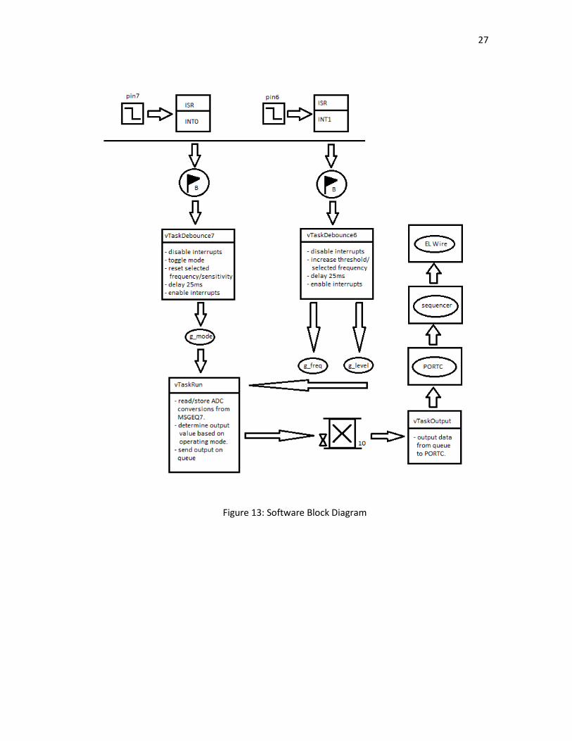
G. Software:
The software was integrated into the final system seamlessly. Initial software tests using
the LEDs on the STK500 were successful. Sweeping the 100mVpp sinusoid across the audio
frequency range yielded expected results based on the data in Table I and the chosen
threshold level for the system. The system was interfaced with the EL wire sequencer
without issue once the LED tests were complete. A software diagram for the final design is
shown below in Figure 13.
27
Figure 13: Software Block Diagram

28
H. Final System Revision:
The final system design is represented as a block diagram in Figure 14 below.
Figure 14: Revised System Block Diagram

29
VIII. Conclusion
Overall, the final implementation of the Audio-Triggered EL Wire Sequencer was successful,
although several design and requirement changes were necessary due to the limitations of
the available hardware. These limitations included the switching speed of the TRIACs, the
source voltage limits of the optoisolator TRIACs, the available memory on the ATMega32A
microcontroller, and the maximum clock rate of the ADC on the ATMega32A. As a result of
these PWM could not be used to represent a signals magnitude, modifications needed to be
made to the PCB to accommodate TRIACs, and a graphic equalizer display filter substituted
for an FFT implementation.
The performance of the resulting system is exceptional in spite of the changes made to the
original system. When synchronized with an audio signal, the EL wire reacts in real time –
with the total response time under 51ms (virtually identical to the response time listed in
the requirements). All of the operating modes and corresponding controls function as
expected without issue.

30
IX. Bibliography
[1] "A History of Electroluminescent Displays." Indiana University. Web. 09 June 2011.
<http://www.indiana.edu/~hightech/fpd/papers/ELDs.html>.
[2] "Electroluminescence." Wikipedia, the Free Encyclopedia. Web. 09 June 2011.
<http://en.wikipedia.org/wiki/Electroluminescent>.
[3] "What Is Electroluminescent Wire." Welcome to Elwire.com Your EL Wire, Aka
Electroluminescent Wire Source. A Glowing String / Wire / Cable / Rope / Fiber like Material.
Web. 09 June 2011. <http://www.elwire.com/whatis.html>.
[4] "EL Wire FAQ." Welcome to Elwire.com Your EL Wire, Aka Electroluminescent Wire
Source. A Glowing String / Wire / Cable / Rope / Fiber like Material. Web. 09 June 2011.
<http://www.elwire.com/faq/faq.html>.
[5] STMicroelectronics Z0103MA Datasheet. Standard 1A Triacs. Geneva, Switzerland,
2010. Retrieved June 9, 2011 from http://www.st.com/stonline/books/pdf/docs/7474.pdf
[6] Texas Instruments moc3022 Datasheet. Optoisolator Triac. Texas, 1998. Retrieved June
9, 2011 from http://focus.ti.com/lit/ds/symlink/moc3022.pdf
[7] Atmel ATMega32A Datasheet. 8-bit AVR Microcontroller with 32Kbytes In-System
Programmable Flash. San Jose, 2011. Retrieved June 9, 2011 from
http://www.atmel.com/dyn/resources/prod_documents/doc8155.pdf
[8] "Electronics Experiments: Audio Amplifiers." Electronix Express - Electronics for Schools
and Industry. Web. 09 June 2011. <http://www.elexp.com/t_audio.htm>.
[9] Mixed Signal Integration MSGEQ7 Datasheet. Seven Band Graphic Equalizer Display
Filter. San Jose, 2004.
[10] FreeRTOS-A Free Professional Grade RTOS Supporting 27 Architectures, including
ARM7, ARM9, Cortex-M3, RX600, MSP430, MSP430X, MicroBlaze, AVR, X86, PIC32, PIC24,
DsPIC, H8S, HCS12 and 8051. Web. 09 June 2011. <http://www.freertos.org/>.
[11] Sparkfun Electronics COM-09765 Datasheet. Serial 7-Segment Display. Boulder,
Colorado, 2010. Retrieved June 9, 2011 from
http://www.sparkfun.com/datasheets/Components/LED/7-Segment/SFE-0012-DS-
7segmentSerial-v41.pdf

31
Appendices
A. Specifications (requirements)
System:
3. The system will receive an audio signal via standard 3.5mm TRS connector (i.e. minijack)
that will serve as the input to the system.
4. The system shall operate in two modes which can be selected with a mode button.
5. The output of the system shall consist of six strands of differently colored EL wire, each
with common threshold and unique frequency band (MODE 1).
6. The output of the system shall consist of six strands of differently colored EL wire which
all have a unique threshold and share a frequency selected by a frequency button
(MODE 2). The frequency defaults to the lowest frequency once the mode is entered
and is incremented up as the frequency button is pressed (the frequency rolls over to
the lowest frequency after the highest frequency is selected).
7. The system shall consist of three main subsystems that allow it to operate properly: the
sequencer, the spectrum analyzer, and the software.

32
Subsystems:
Sequencer:
1. The sequencer will interface between the six strands of EL wire, the AC source,
and the microcontroller.
2. The sequencer will have seven lines that connect to the microcontroller port.
These include a common ground and six control lines that can route the
corresponding EL wire to the AC source when a 5V signal is applied to the input
pin.
3. The 5V input signal should be current limited to under 20mA so that in can be
sourced by the microcontroller.
4. The control lines shall all be active HIGH.
Spectrum Analyzer:
1. The spectrum analyzer shall produce a minimum of six frequency bands – one
for each strand of EL wire (For FFT implementation, this corresponds to a
minimum length of N=8)
2. The spectrum analyzer shall span frequencies within the audible range (<20kHz)
with a maximum frequency of at least 16kHz.
3. According to the sampling theorem, the sample rate of the spectrum analyzer
must be at least 32kHz in order to recover the 16kHz maximum frequency.
Software:

33
1. The software must handle the operation of all subsystems in real time (this
means running the spectrum analyzer and updating to the EL wire sequencer in
under 50ms every cycle).
2. The software must also implement the user interface. This means handling the
mode switching, threshold switching (in MODE 1), frequency switching (in
MODE 2), and button debouncing.

34
B. Parts List and Costs
Item Quantity Unit Cost Total Cost
EL wire(5ft. 2mm) 6 $8.75 $52.5
EL wire driver (50ft.) 1 $18.95 $18.95
Optoisolator TRIAC 6 $1.00 $6.00
511-Z0103MA TRIAC 6 $0.54 $3.24
1k Ohm resistors 6 $0.15 $0.90
20nF capacitor 1 $0.24 $0.24
2-pin Molex connector
7 $0.70 $4.90
7-pin Molex header 1 $1.25 $1.25
sequencer PCB 3 $30.47 $91.41
MSGEQ7 1 $4.95 $4.95
TRS connector 1 $1.25 $1.25
0.1uF capacitor 2 $0.25 $0.50
0.01uF capacitor 1 $0.22 $0.22
33pF capacitor 1 $0.25 $0.25
200k Ohm resistor 1 $0.20 $0.20
741 Op Amp 1 $0.80 $0.80
10k Ohm resistors 4 $0.10 $0.40
10uF capacitor 1 $1.29 $1.29
1uF capacitor 1 $1.09 $1.09
STK500 w/ ATMega32A
1 N/A N/A
7-segment serial display
1 $12.95 $12.95
3/8x36” rod thread 4 $11.99 $47.96
36x7/32 brass tube 4 3.99 $15.96
fasteners 12 $0.26 $3.12
brass wing nut 1 $2.25 $2.25
aluminum plates 3 N/A N/A
willow pieces 3 N/A N/A
Table III: Parts List and Costs
35
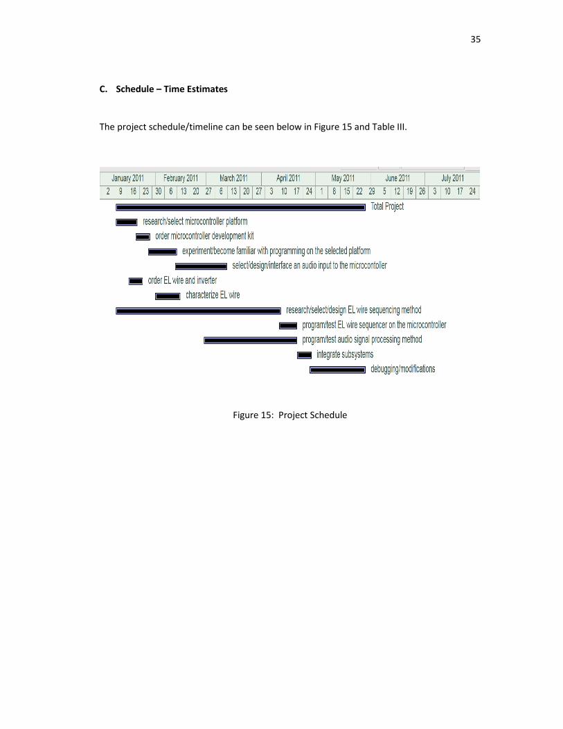
C. Schedule – Time Estimates
The project schedule/timeline can be seen below in Figure 15 and Table III.
Figure 15: Project Schedule

36
Table IV: Project Schedule

37
D. PC Board Layout
Figure 16: PCB layout
38
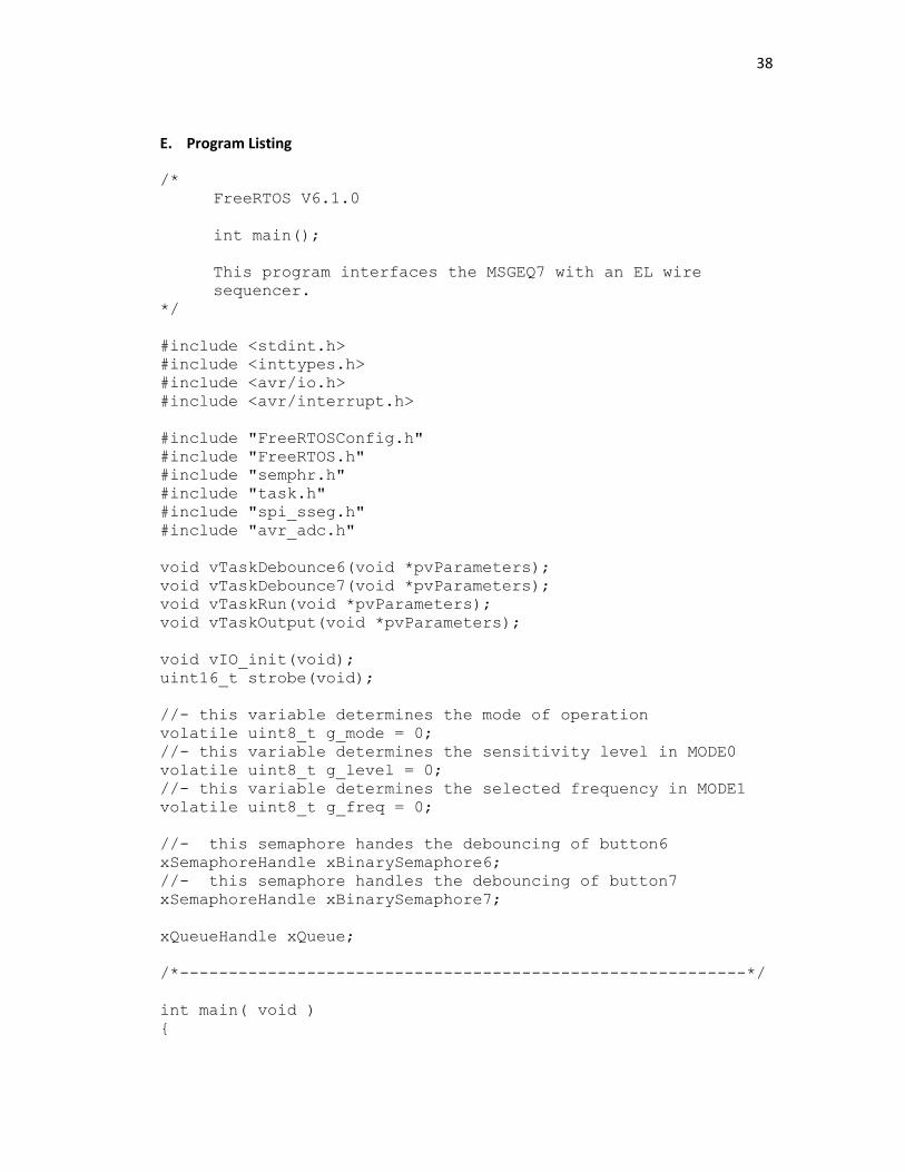
E. Program Listing
/*
FreeRTOS V6.1.0
int main();
This program interfaces the MSGEQ7 with an EL wire
sequencer.
*/
#include <stdint.h>
#include <inttypes.h>
#include <avr/io.h>
#include <avr/interrupt.h>
#include "FreeRTOSConfig.h"
#include "FreeRTOS.h"
#include "semphr.h"
#include "task.h"
#include "spi_sseg.h"
#include "avr_adc.h"
void vTaskDebounce6(void *pvParameters);
void vTaskDebounce7(void *pvParameters);
void vTaskRun(void *pvParameters);
void vTaskOutput(void *pvParameters);
void vIO_init(void);
uint16_t strobe(void);
//- this variable determines the mode of operation
volatile uint8_t g_mode = 0;
//- this variable determines the sensitivity level in MODE0
volatile uint8_t g_level = 0;
//- this variable determines the selected frequency in MODE1
volatile uint8_t g_freq = 0;
//- this semaphore handes the debouncing of button6
xSemaphoreHandle xBinarySemaphore6;
//- this semaphore handles the debouncing of button7
xSemaphoreHandle xBinarySemaphore7;
xQueueHandle xQueue;
/*----------------------------------------------------------*/
int main( void )
{
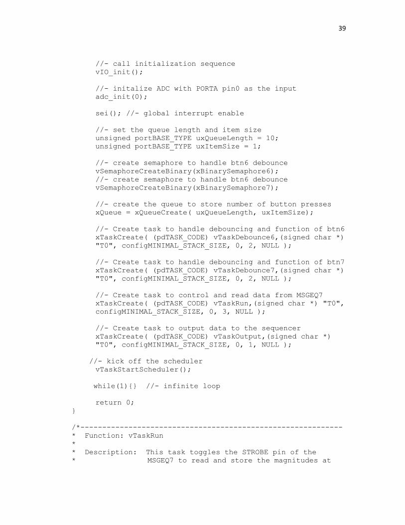
39
//- call initialization sequence
vIO_init();
//- initalize ADC with PORTA pin0 as the input
adc_init(0);
sei(); //- global interrupt enable
//- set the queue length and item size
unsigned portBASE_TYPE uxQueueLength = 10;
unsigned portBASE_TYPE uxItemSize = 1;
//- create semaphore to handle btn6 debounce
vSemaphoreCreateBinary(xBinarySemaphore6);
//- create semaphore to handle btn6 debounce
vSemaphoreCreateBinary(xBinarySemaphore7);
//- create the queue to store number of button presses
xQueue = xQueueCreate( uxQueueLength, uxItemSize);
//- Create task to handle debouncing and function of btn6
xTaskCreate( (pdTASK_CODE) vTaskDebounce6,(signed char *)
"T0", configMINIMAL_STACK_SIZE, 0, 2, NULL );
//- Create task to handle debouncing and function of btn7
xTaskCreate( (pdTASK_CODE) vTaskDebounce7,(signed char *)
"T0", configMINIMAL_STACK_SIZE, 0, 2, NULL );
//- Create task to control and read data from MSGEQ7
xTaskCreate( (pdTASK_CODE) vTaskRun,(signed char *) "T0",
configMINIMAL_STACK_SIZE, 0, 3, NULL );
//- Create task to output data to the sequencer
xTaskCreate( (pdTASK_CODE) vTaskOutput,(signed char *)
"T0", configMINIMAL_STACK_SIZE, 0, 1, NULL );
//- kick off the scheduler
vTaskStartScheduler();
while(1){} //- infinite loop
return 0;
}
/*------------------------------------------------------------
* Function: vTaskRun
*
* Description: This task toggles the STROBE pin of the
* MSGEQ7 to read and store the magnitudes at

40
* each frequency. It then outputs results to
* PORTC according to the mode of operation.
------------------------------------------------------------*/
void vTaskRun(void *pvParameters)
{
PORTD &= ~_BV(1); //-initialize STROBE line LOW
//- create array to store magnitudes of each frequency
//- band
static uint16_t adc_result[7];
//- create local counting variables
static uint8_t i = 0;
static uint8_t j = 0;
//- create variable to store result to be output on LEDs
static uint8_t outputs = 0x00; //- sequencer init
//- this look up table stores values for the ADC result
//- to be compared to
static const threshold[10] = \
{100,200,300,400,500,600,700,800,900,1000};
for(;;)
{
//- read all frequency bands from MSGEQ7 and store
//- values in adc_result array
//- (63Hz,160Hz,400Hz,1kHz,2.5kHz,6.25kHz,16kHz
//- correspond to i=0 to i=6)
for(i=0;i<7;i++)
{
adc_result[i] = strobe();
}
//- reset outputs variable for next iteration
outputs = 0x00;
//- determine outputs for mode0 (all frequencies
//- with low magnitude resolution)
if(g_mode == 0)
{
for(j=0;j<7;j++)
{
//- compare all frequencies to selected
//- threshold level
if(adc_result[j] > threshold[g_level])

41
{
//- set bit if frequency's
//- magnitude exceeds the threshold
outputs |= _BV(j);
}
}
}
//- determine outputs for mode1 (single frequency
//- with high magnitude resolution)
else if(g_mode == 1)
{
for(j=0;j<8;j++)
{
//- compare selected frequency's
//- magnitude to all threshold values
if(adc_result[g_freq] > threshold[j])
{
//- set bit if selected frequency's
//- magnitude exceeds the threshold
outputs |= _BV(j);
}
}
}
//- send output data to Output task via the queue
xQueueSend(xQueue, &outputs, 0);
}
}
/*------------------------------------------------------------
* Function: vTaskOutput
*
* Description: This task takes data from the Run task via
* the queue and outputs the result on PORTC.
* The queue will block if there is no new data
* to receive.
------------------------------------------------------------*/
void vTaskOutput(void *pvParameters)
{
static uint8_t outputs = 0; //- store queue data
for(;;)
{
//- store data from the queue locally onto outputs
xQueueReceive(xQueue, &outputs, portMAX_DELAY);
PORTC = outputs; //- output result to PORTC
42
}
}
/*------------------------------------------------------------
* Function: vTaskDebounce6
*
* Description: This task debounces btn6 and increments the
* threshold(sensitivity) or the selected
* frequency depending on the mode.
------------------------------------------------------------*/
void vTaskDebounce6(void *pvParameters)
{
//- take semaphore once at program start to start at 0
xSemaphoreTake(xBinarySemaphore6, portMAX_DELAY);
for(;;)
{
//- take semaphore once at program start to start
//- at 0
if(xSemaphoreTake(xBinarySemaphore6, portMAX_DELAY)
== pdPASS)
{
cli(); //- disable interrupts
//- increment the threshold (lower
//- sensitivity) in mode0
if(g_mode == 0)
{
g_level++;
//- reset to 0
if(g_level == 9) g_level = 0;
}
//- increment the selected frequency in mode1
else if(g_mode == 1)
{
g_freq++;
//- reset to 0
if(g_freq == 7) g_freq = 0;
}
//- delay until btn6 is debounced
vTaskDelay(25 / portTICK_RATE_MS );
sei(); //- enable interrupts after delay
}
}
}
/*------------------------------------------------------------
43
* Function: vTaskDebounce7
*
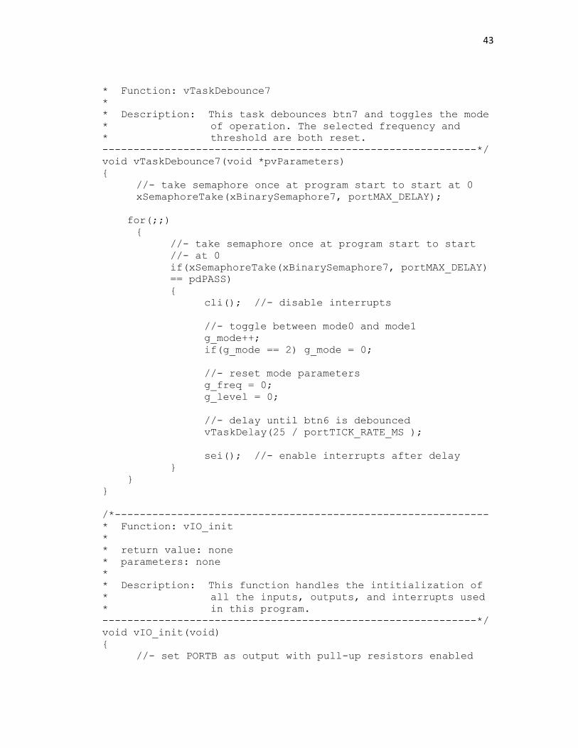
* Description: This task debounces btn7 and toggles the mode
* of operation. The selected frequency and
* threshold are both reset.
------------------------------------------------------------*/
void vTaskDebounce7(void *pvParameters)
{
//- take semaphore once at program start to start at 0
xSemaphoreTake(xBinarySemaphore7, portMAX_DELAY);
for(;;)
{
//- take semaphore once at program start to start
//- at 0
if(xSemaphoreTake(xBinarySemaphore7, portMAX_DELAY)
== pdPASS)
{
cli(); //- disable interrupts
//- toggle between mode0 and mode1
g_mode++;
if(g_mode == 2) g_mode = 0;
//- reset mode parameters
g_freq = 0;
g_level = 0;
//- delay until btn6 is debounced
vTaskDelay(25 / portTICK_RATE_MS );
sei(); //- enable interrupts after delay
}
}
}
/*------------------------------------------------------------
* Function: vIO_init
*
* return value: none
* parameters: none
*
* Description: This function handles the intitialization of
* all the inputs, outputs, and interrupts used
* in this program.
------------------------------------------------------------*/
void vIO_init(void)
{
//- set PORTB as output with pull-up resistors enabled

44
DDRB = 0xFF;
PORTB = 0xFF;
//- set PORTC as output with pull-up resistors enabled
DDRC = 0xFF;
PORTC = 0xFF;
//- pins 2,3 as input 0,1 as outputs
DDRD = (0<<2)|(0<<3)|(1<<0)|(1<<1);
PORTD = 0xFF; //- set pull-up resistors on PORTD
//- enable external interrupts
GICR |= (1<<INT1)|(1<<INT0);
}
/*------------------------------------------------------------
* Function: strobe
*
* return value: ADC reading for the selected channel on the
* MSGEQ7
*
* parameters: none
*
* Description: This function generates the square wave on
* the STROBE pin of the MSGEQ7 and returns the
* ADC reading from the DC output of the chip.
------------------------------------------------------------*/
uint16_t strobe(void)
{
PORTD |= _BV(1); //- square wave HIGH
//- first half square wave period
vTaskDelay(1 / portTICK_RATE_MS );
PORTD &= ~_BV(1); //- square wave LOW
//- second half square wave period
vTaskDelay(1 / portTICK_RATE_MS );
return read_adc(); //- store ADC result in array
}
//- ISR for btn7
ISR (INT0_vect)
{
static portBASE_TYPE xHigherPriorityTaskWoken;
xHigherPriorityTaskWoken = pdFALSE;
xSemaphoreGiveFromISR( xBinarySemaphore6,
&xHigherPriorityTaskWoken );
45
}
//- ISR for btn6
ISR (INT1_vect)
{
static portBASE_TYPE xHigherPriorityTaskWoken;
xHigherPriorityTaskWoken = pdFALSE;
//- pass semaphore to debounce task
xSemaphoreGiveFromISR( xBinarySemaphore7,
&xHigherPriorityTaskWoken );
}
/* -----------------------------------------------------------
* Filename: avr_adc.h
*
* This file provides support for the associated ".c" file.
* The function headers should be the same for both files.
*
*-----------------------------------------------------------*/
//------------------------------------------------------------
//- Function: adc_init()
//-
//- return value: none
//- parameters: PORTA pins that will be ADC inputs
//-
//- Description: Initializes the ADC with 5V reference voltage
//- and a clock divider of 8.
//------------------------------------------------------------
void adc_init(uint8_t);
//------------------------------------------------------------
//- Function: read_adc()
//-
//- return value: 10-bit ADC result
//- parameters: none
//-
//- Description: This function initializes and ADC conversion,
//- waits for the conversion to be complete, and returns the
//- 10-bit result typecast as an unsigned 16-bit integer.
//------------------------------------------------------------
uint16_t read_adc(void);
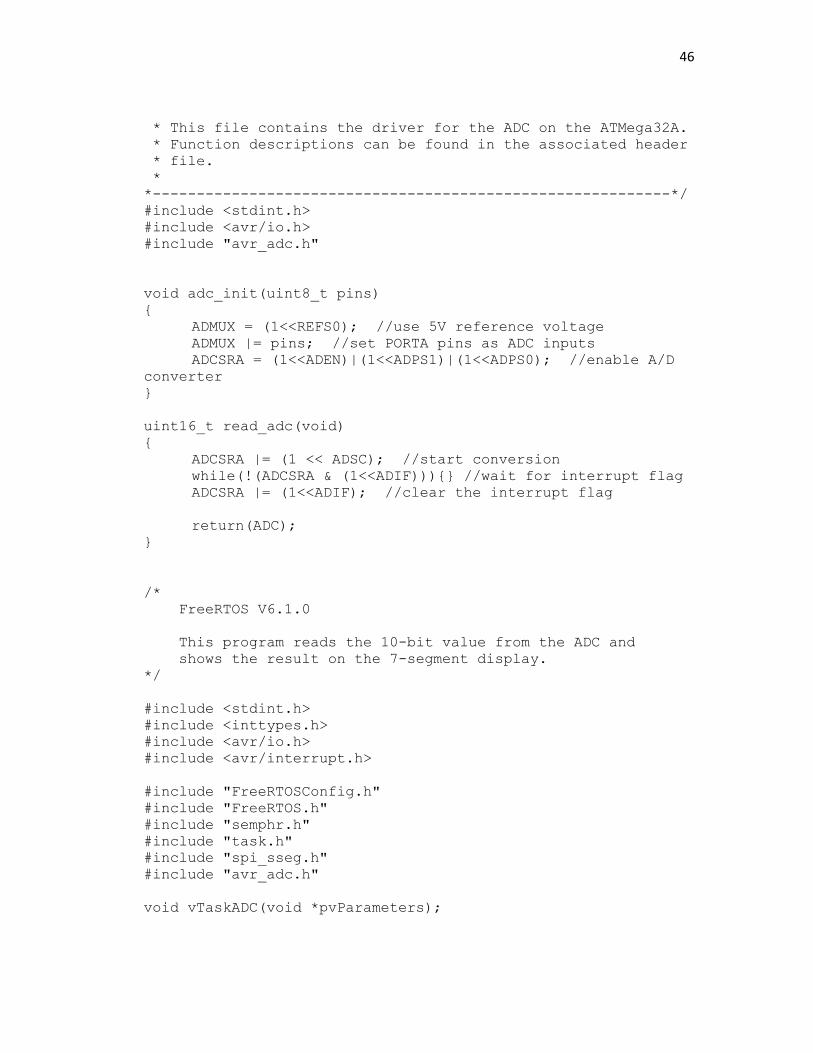
/* -----------------------------------------------------------
* Filename: avr_adc.c
*
46
* This file contains the driver for the ADC on the ATMega32A.
* Function descriptions can be found in the associated header
* file.
*
*-----------------------------------------------------------*/
#include <stdint.h>
#include <avr/io.h>
#include "avr_adc.h"
void adc_init(uint8_t pins)
{
ADMUX = (1<<REFS0); //use 5V reference voltage
ADMUX |= pins; //set PORTA pins as ADC inputs
ADCSRA = (1<<ADEN)|(1<<ADPS1)|(1<<ADPS0); //enable A/D
converter
}
uint16_t read_adc(void)
{
ADCSRA |= (1 << ADSC); //start conversion
while(!(ADCSRA & (1<<ADIF))){} //wait for interrupt flag
ADCSRA |= (1<<ADIF); //clear the interrupt flag
return(ADC);
}
/*
FreeRTOS V6.1.0
This program reads the 10-bit value from the ADC and
shows the result on the 7-segment display.
*/
#include <stdint.h>
#include <inttypes.h>
#include <avr/io.h>
#include <avr/interrupt.h>
#include "FreeRTOSConfig.h"
#include "FreeRTOS.h"
#include "semphr.h"
#include "task.h"
#include "spi_sseg.h"
#include "avr_adc.h"
void vTaskADC(void *pvParameters);
47
/*----------------------------------------------------------*/
int main( void )
{
SPI_MasterInit();
//- call initialization sequence
vIO_init();
//- initalize ADC with PORTA pin0 as the input
adc_init(0);
//- global interrupt enable
sei();
//- Create task to output data to the sequencer
xTaskCreate( (pdTASK_CODE) vTaskADC,(signed char *) "T0",
configMINIMAL_STACK_SIZE, 0, 1, NULL );
//- kick off the scheduler
vTaskStartScheduler();
while(1){}
return 0;
}
/*------------------------------------------------------------
* Function: vTaskADC
*
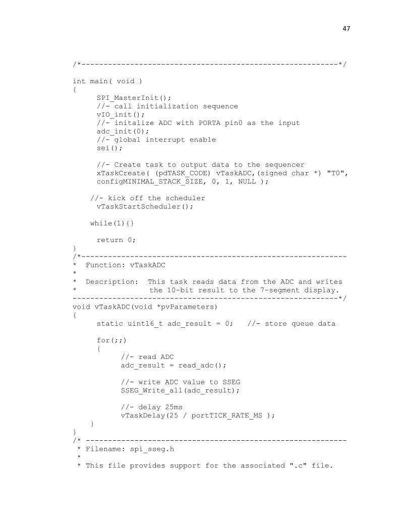
* Description: This task reads data from the ADC and writes
* the 10-bit result to the 7-segment display.
------------------------------------------------------------*/
void vTaskADC(void *pvParameters)
{
static uint16_t adc_result = 0; //- store queue data
for(;;)
{
//- read ADC
adc_result = read_adc();
//- write ADC value to SSEG
SSEG_Write_all(adc_result);
//- delay 25ms
vTaskDelay(25 / portTICK_RATE_MS );
}
}
/* -----------------------------------------------------------
* Filename: spi_sseg.h
*
* This file provides support for the associated ".c" file.

48
* The function headers should be the same for both files.
* While not optimal, that seemed like the best thing to do at
* the moment.
*
* -bryan (mealy) 2011
*----------------------------------------------------------*/
//----------------------------------------------
//- This driver uses the following:
//- PB4 as the chip select (arbitrary)
//- PB5 as the MOSI output
//- PB7 as the clock output
//----------------------------------------------
#define SPI_SS 4
#define SPI_MOSI 5
#define SPI_SCK 7
// various escape code stuff for the 7-seg display
#define SSEG_BRIGHTNESS 0x7A
#define SSEG_RESET 0x76
#define SSEG_SPACE 0x78
#define SSEG_DEC_PNT 0x77
//- date used to turn on individual bits for 0-F
//- plus everything off (final value)
#define SSEG_0 0x3F
#define SSEG_1 0x06
#define SSEG_2 0x5B
#define SSEG_3 0x4F
#define SSEG_4 0x66
#define SSEG_5 0x6D
#define SSEG_6 0x7D
#define SSEG_7 0x07
#define SSEG_8 0x7F
#define SSEG_9 0x67
#define SSEG_A 0x77
#define SSEG_B 0x7C
#define SSEG_C 0x79
#define SSEG_D 0x5E
#define SSEG_E 0x79
#define SSEG_F 0x71
#define SSEG_BLANK 0x00
//- decimal point stuff
#define SSEG_DP_0 (0x01 << 0) //- digit1 DP
#define SSEG_DP_1 (0x01 << 1) //- digit2 DP
#define SSEG_DP_2 (0x01 << 2) //- digit3 DP

49
#define SSEG_DP_3 (0x01 << 3) //- digit4 DP
#define SSEG_DP_4 (0x01 << 4) //- colon between digits two
and three
#define SSEG_DP_5 (0x01 << 5) //- digit3 degree
//- DIGIT_1 is the left-most display
#define DIGIT_1 0x01
#define DIGIT_2 0x02
#define DIGIT_3 0x03
#define DIGIT_4 0x04
//- escape code for individual 7-segment digits
//- DIG1 is the left-most digit
#define SSEG_DIG1 0x7B
#define SSEG_DIG2 0x7C
#define SSEG_DIG3 0x7D
#define SSEG_DIG4 0x7E
#define LED0 0x00
#define LED2 0x02
//------------------------------------------------------------
//- Function: SPI_MasterInit()
//-
//- return value: none
//- parameters: none
//-
//- Description: Initializes the AVR device as a master and
//- and turns on the device and sets the clock frequency.
//- For convenience, this function also configures the SPI
//- port GPIOs
//------------------------------------------------------------
void SPI_MasterInit(void);
//------------------------------------------------------------
//- Function: SPI_MasterTransmit()
//-
//- return value: none
//- parameters: data to be transmitted
//-
//- Description: This function selects the device, transmits
//- the data, waits for a the transmission to complete with
//- a poll, then deselects the device.

50
//------------------------------------------------------------
void SPI_MasterTransmit(uint8_t data);
//------------------------------------------------------------
//- Function: SSEG_Set_Brightness()
//-
//- return value: none
//- parameters: val, the value to set the brightness of
//- display.
//-
//- Description: This function set the brightness of the
//- display where 255 is off and 0 is on as bright as
//- possible.
//------------------------------------------------------------
void SSEG_Set_Brightness(uint8_t val);
//------------------------------------------------------------
//- Function: SSEG_Reset()
//-
//- return value: none
//- parameters: none
//-
//- Description: This function turns off all display elements.
//------------------------------------------------------------
void SSEG_Reset(void);
//------------------------------------------------------------
//- Function: SSEG_Write_digit()
//-
//- return value: none
//- parameters: digit location and digit value
//-
//- Description: This is a wrapper function for writing
//- individual digits to the display. In this case, you need
//- to first send the initial escape character before you
//- send the actual data.
//------------------------------------------------------------
void SSEG_Write_digit(uint8_t digit, uint8_t val);
//------------------------------------------------------------
//- Function: SSEG_Write_left_digits()
51
//-
//- return value: none
//- parameters: binary value for display on two left-most
//- digits
//-
//- Description: This function decomposes the sent value into
//- a tens and ones digit the then sends them off to the two
//- left-most digits of the display. This function also
//- handles lead zero blanking.
//------------------------------------------------------------
void SSEG_Write_left_digits(uint8_t val);
//------------------------------------------------------------
//- Function: SSEG_Write_right_digits()
//-
//- return value: none
//- parameters: binary value for display on two right-most
//- digits
//-
//- Description: This function decomposes the sent value into
//- a tens and ones digit the then sends them off to the two
//- right-most digits of the display. This function also
//- handles lead zero blanking.
//------------------------------------------------------------
void SSEG_Write_right_digits(uint8_t val);
//------------------------------------------------------------
//- Function: SSEG_Write_right_digits()
//-
//- return value: none
//- parameters: binary value for display on two right-most
//- digits
//-
//- Description: This function decomposes the sent value into
//- a tens and ones digit the then sends them off to the two
//- right-most digits of the display. This function also
//- handles lead zero blanking.
//------------------------------------------------------------
void SSEG_Write_all(uint16_t val);
/* -----------------------------------------------------------
* Filename: spi_sseg.c
*
* This file is the c file for the 7-segment display driver.

52
*
*----------------------------------------------------------*/
#include <stdint.h>
#include <inttypes.h>
#include <avr/io.h>
#include <avr/interrupt.h>
#include "spi_sseg.h"
void SPI_MasterInit(void)
{
//- set DDR for SPI and LEDs
DDRB = (1<<SPI_MOSI)|(1<<SPI_SCK)|(1<<SPI_SS);
//- enable SPI, set as master, set SCK frequency
SPCR = (1<<SPE)|(1<<MSTR)|(1<<SPR0);
//- initialize chip select and LEDs HIGH
PORTB |= (1<<SPI_SS);
}
void SPI_MasterTransmit(uint8_t data)
{
//- chip select active LOW
PORTB &= ~(1<<SPI_SS);
//- put data in data register
SPDR = data;
//- wait for transmit to complete
while(!(SPSR & (1<<SPIF))){}
//- chip select HIGH
PORTB |= (1<<SPI_SS);
}
void SSEG_Set_Brightness(uint8_t val)
{
//- set brightness to some value from 0 to 255
SPI_MasterTransmit(SSEG_BRIGHTNESS);
SPI_MasterTransmit(val);
}
void SSEG_Reset(void)
{
//- reset SPI port
SPI_MasterTransmit(SSEG_RESET);
}
void SSEG_Write_digit(uint8_t digit, uint8_t val)
{
//- select which 7-segment to write to
53
switch(digit)
{
case 1:
SPI_MasterTransmit(SSEG_DIG1);
break;
case 2:
SPI_MasterTransmit(SSEG_DIG2);
break;
case 3:
SPI_MasterTransmit(SSEG_DIG3);
break;
case 4:
SPI_MasterTransmit(SSEG_DIG4);
break;
default:
SPI_MasterTransmit(SSEG_DIG1);
break;
}
//- write value to selected digit
switch(val)
{
case 0:
SPI_MasterTransmit(SSEG_0);
break;
case 1:
SPI_MasterTransmit(SSEG_1);
break;
case 2:
SPI_MasterTransmit(SSEG_2);
break;
case 3:
SPI_MasterTransmit(SSEG_3);
break;
case 4:
SPI_MasterTransmit(SSEG_4);
break;
case 5:
SPI_MasterTransmit(SSEG_5);
break;
case 6:
SPI_MasterTransmit(SSEG_6);
break;
case 7:
SPI_MasterTransmit(SSEG_7);
break;
case 8:
SPI_MasterTransmit(SSEG_8);
break;
case 9:

54
SPI_MasterTransmit(SSEG_9);
break;
case 10:
SPI_MasterTransmit(SSEG_A);
break;
case 11:
SPI_MasterTransmit(SSEG_B);
break;
case 12:
SPI_MasterTransmit(SSEG_C);
break;
case 13:
SPI_MasterTransmit(SSEG_D);
break;
case 14:
SPI_MasterTransmit(SSEG_E);
break;
case 15:
SPI_MasterTransmit(SSEG_F);
break;
default:
SPI_MasterTransmit(SSEG_BLANK);
break;
}
}
void SSEG_Write_left_digits(uint8_t val)
{
uint8_t tens, ones;
//- find ten's place value
tens = val/10;
//- find one's place value
ones = val%10;
//- if ten's place is zero, blank digit
if(tens == 0)
{
SSEG_Write_digit(DIGIT_1, 16);
//- if one's is also zero, blank digit
if(ones == 0)
{
SSEG_Write_digit(DIGIT_2, 16);
}
else
{
//- write one's value otherwise
SSEG_Write_digit(DIGIT_2, ones);

55
}
}
//- write both digits if none are zero
else
{
SSEG_Write_digit(DIGIT_1, tens);
SSEG_Write_digit(DIGIT_2, ones);
}
}
void SSEG_Write_right_digits(uint8_t val)
{
uint8_t tens, ones;
//- find ten's place value
tens = val/10;
//- find one's place value
ones = val%10;
//- blank digit if ten's is zero
if(tens == 0)
{
SSEG_Write_digit(DIGIT_3, 16);
}
//- write ten's value otherwise
else
{
SSEG_Write_digit(DIGIT_3, tens);
}
//- write one's place
SSEG_Write_digit(DIGIT_4, ones);
}
void SSEG_Write_all(uint16_t val)
{
uint8_t right, left;
//- find thousanth's/hundredth's place
left = val/100;
//- find ten's/one's place
right = val%100;
//- write left/right to display
SSEG_Write_left_digits(left);
SSEG_Write_right_digits(right);
}
56
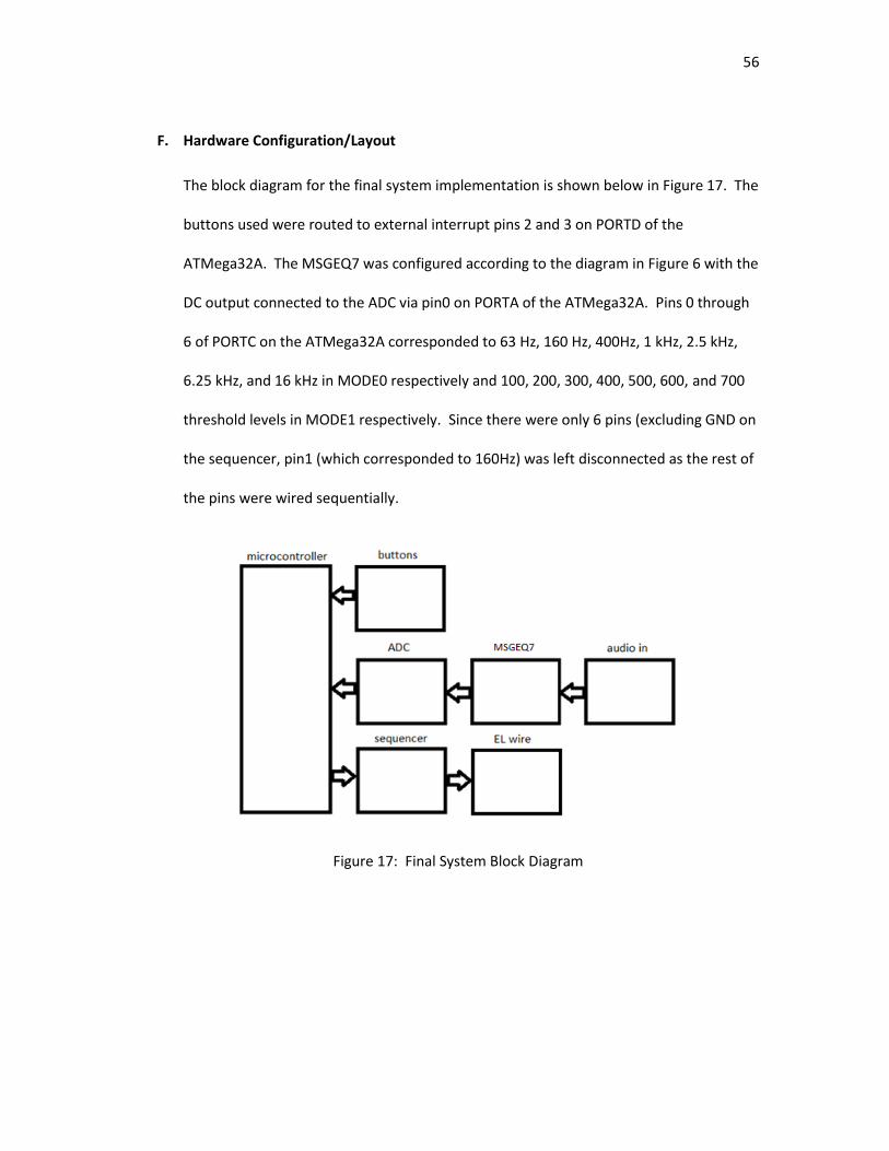
F. Hardware Configuration/Layout
The block diagram for the final system implementation is shown below in Figure 17. The
buttons used were routed to external interrupt pins 2 and 3 on PORTD of the
ATMega32A. The MSGEQ7 was configured according to the diagram in Figure 6 with the
DC output connected to the ADC via pin0 on PORTA of the ATMega32A. Pins 0 through
6 of PORTC on the ATMega32A corresponded to 63 Hz, 160 Hz, 400Hz, 1 kHz, 2.5 kHz,
6.25 kHz, and 16 kHz in MODE0 respectively and 100, 200, 300, 400, 500, 600, and 700
threshold levels in MODE1 respectively. Since there were only 6 pins (excluding GND on
the sequencer, pin1 (which corresponded to 160Hz) was left disconnected as the rest of
the pins were wired sequentially.
Figure 17: Final System Block Diagram