atomic manipulation by stm nanoscience and nanotechnology 180/198 – 534 peter grutter mcgill...
TRANSCRIPT
Atomic Manipulation by STM
Nanoscience and Nanotechnology 180/198 – 534
Peter GrutterMcGill University
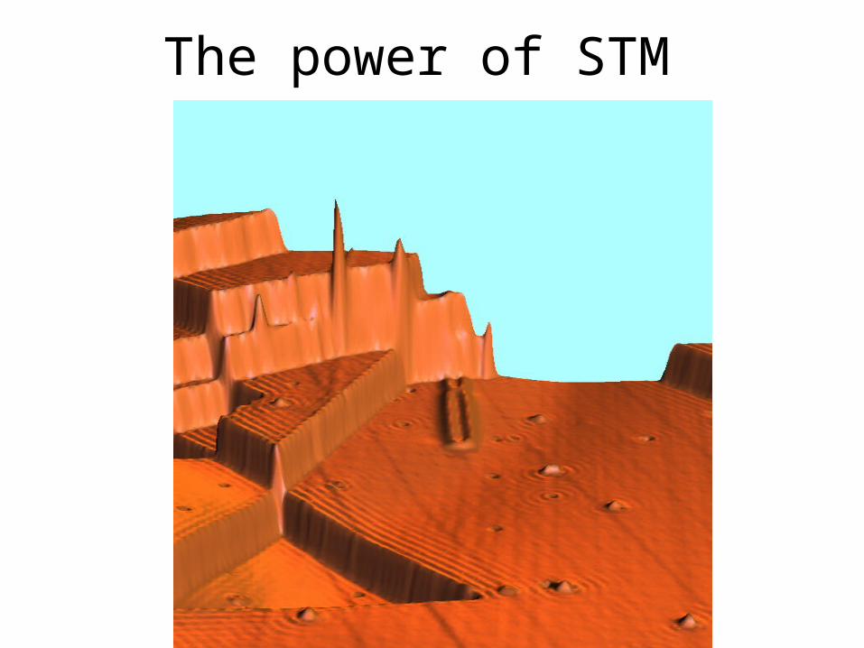
The power of STM

Atomic-scale STM manipulation modes
1. Parallel processe1. Field assisted diffusion
2. Serial Processes1. Sliding
2. Transfer or near contact
3. Field evaporation
4. Electromigration
J. Stroscio and D. Eigler, Science 254, 1319 (1991)
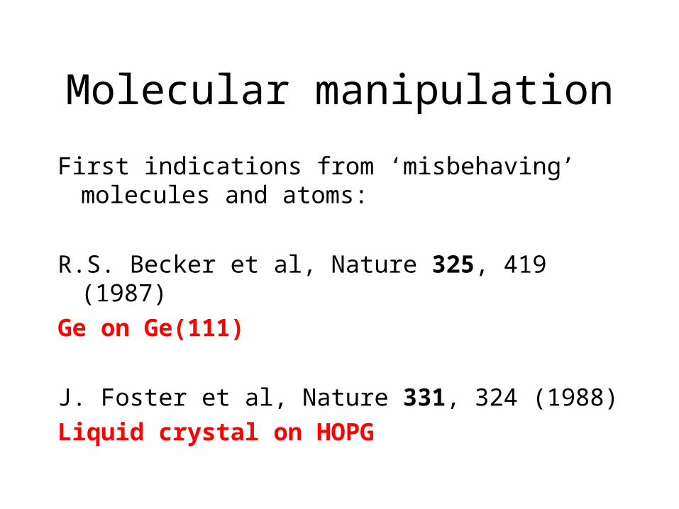
Molecular manipulation
First indications from ‘misbehaving’ molecules and atoms:
R.S. Becker et al, Nature 325, 419 (1987)
Ge on Ge(111)
J. Foster et al, Nature 331, 324 (1988)
Liquid crystal on HOPG
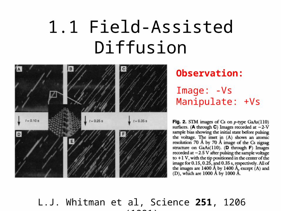
1.1 Field-Assisted Diffusion
L.J. Whitman et al, Science 251, 1206 (1991)
Observation:
Image: -Vs Manipulate: +Vs
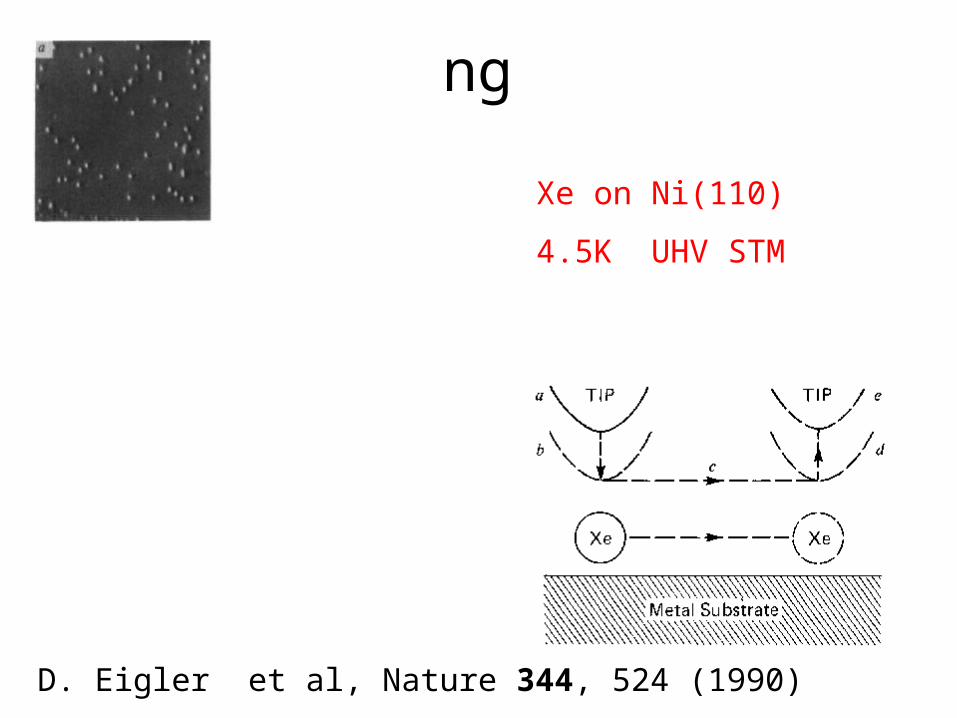
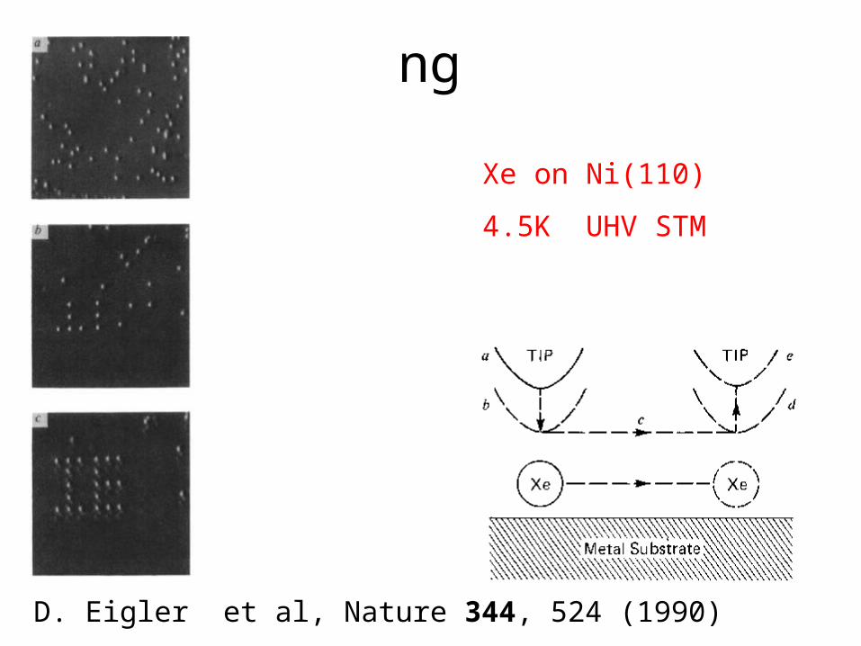
2.1 Sliding
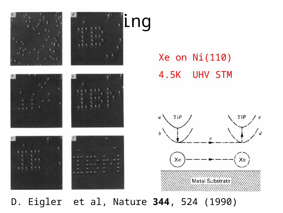
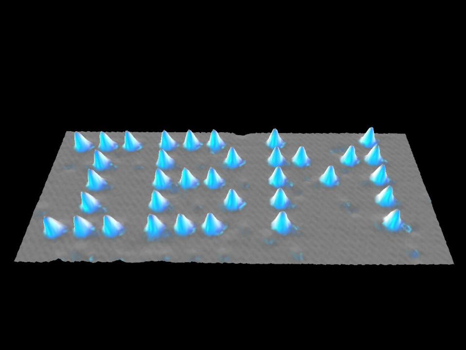
D. Eigler et al, Nature 344, 524 (1990)
Xe on Ni(110)
4.5K UHV STM

2.1 Sliding
D. Eigler et al, Nature 344, 524 (1990)
Xe on Ni(110)
4.5K UHV STM
2.1 Sliding
D. Eigler et al, Nature 344, 524 (1990)
Xe on Ni(110)
4.5K UHV STM
2.1 Sliding
D. Eigler et al, Nature 344, 524 (1990)
Xe on Ni(110)
4.5K UHV STM
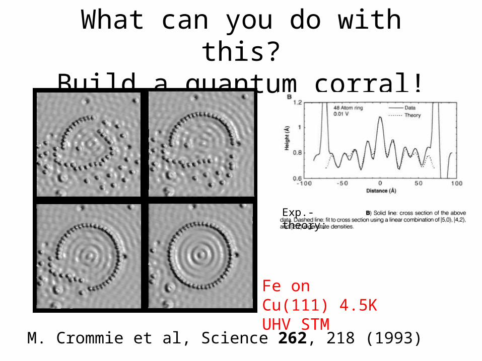
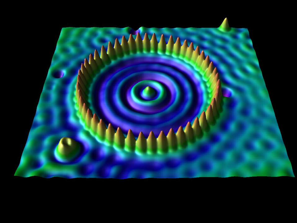
What can you do with this?Build a quantum corral!
M. Crommie et al, Science 262, 218 (1993)
Fe on Cu(111) 4.5K UHV STM
Exp.-theory:

What can you do with a corral?
M. Crommie et al, Science 262, 218 (1993)
Fe on Cu(111) 4.5K UHV STM
Study quantum chaos! (or at least try)

Why do you want to do this?
It’s a nanolab! Study structure – property relationships in nano
systems.
1. Corrugation energies along different x-tal directions (sliding)
2. Strength and sign of interactions in ‘new’, 1D structures, e.g. linear chain of Xe atoms.
3. Big advantage: integrated manipulation, imaging and characterization tool.
4. Many interesting scientific problems, e.g. electrons in confined spaces (corral), information processing, …
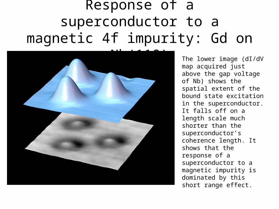
Response of a superconductor to a magnetic 4f impurity: Gd on Nb(110)
The lower image (dI/dV map acquired just above the gap voltage of Nb) shows the spatial extent of the bound state excitation in the superconductor. It falls off on a length scale much shorter than the superconductor’s coherence length. It shows that the response of a superconductor to a magnetic impurity is dominated by this short range effect.

Detection of the magnetic Kondo resonance localized around a single Co atom on Cu(111)
Manoharan, Lutz, and Eigler, Nature 403, 512.515 (2000)
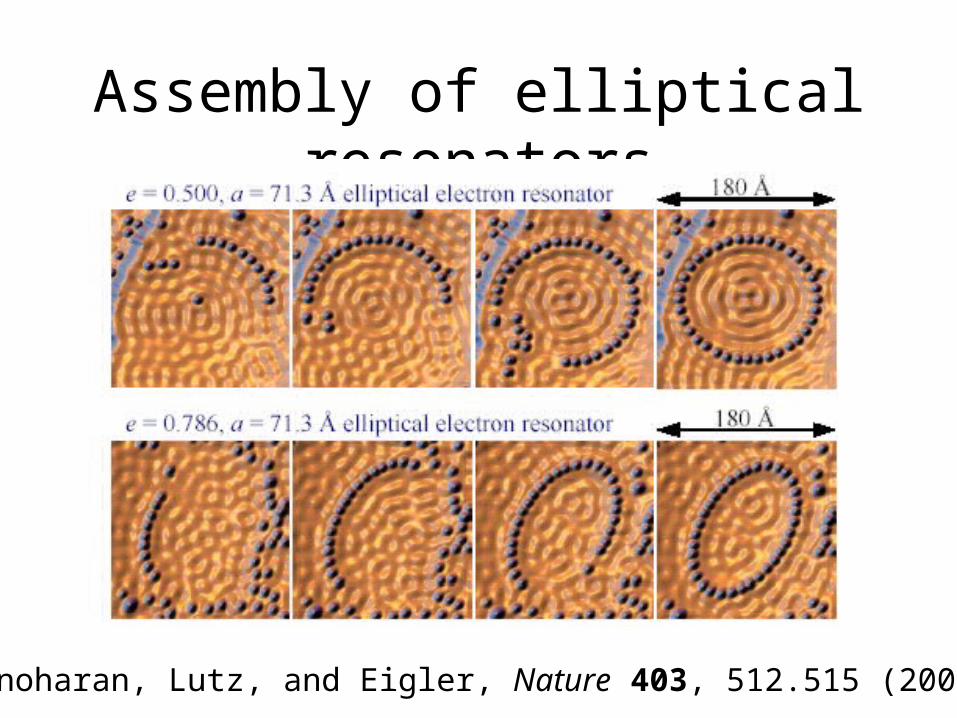
Assembly of elliptical resonators
Manoharan, Lutz, and Eigler, Nature 403, 512.515 (2000)
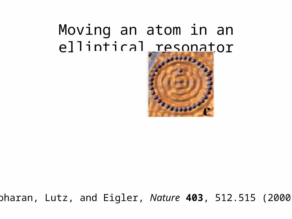
Moving an atom in an elliptical resonator
Manoharan, Lutz, and Eigler, Nature 403, 512.515 (2000)
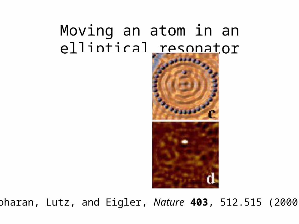
Moving an atom in an elliptical resonator
Manoharan, Lutz, and Eigler, Nature 403, 512.515 (2000)

Moving an atom in an elliptical resonator
Manoharan, Lutz, and Eigler, Nature 403, 512.515 (2000)
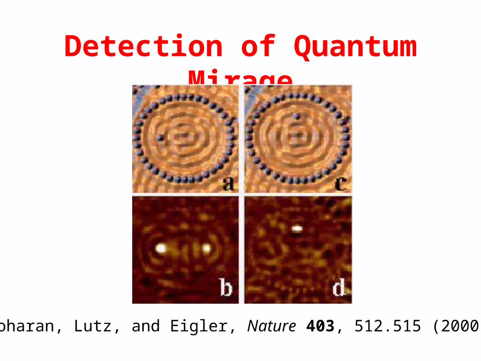
Detection of Quantum Mirage
Manoharan, Lutz, and Eigler, Nature 403, 512.515 (2000)
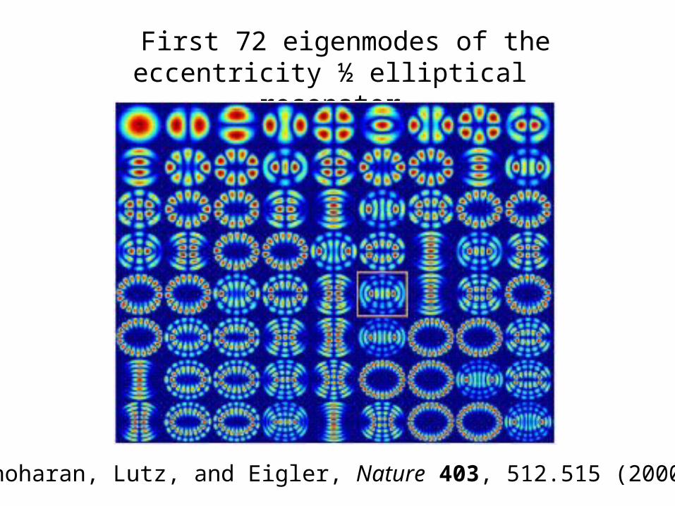
First 72 eigenmodes of the eccentricity ½ elliptical resonator
Manoharan, Lutz, and Eigler, Nature 403, 512.515 (2000)

Sliding molecules at RT
Cu-TBP porphyrin
T.A. Jung et al, Science 271, 181 (1996)
Cu-TP porphyrinon Cu(100) RT UHV STM

A molecular cascade device
A.J.Heinrich et al, Science 298, 1381 (2002)
A prototype for a molecular cascade device. CO molecules are deposited on a Cu(111) surface at 4 K. Individual molecules are imaged as depressions (a).
The red dots mark adsorption sites for CO molecules, whereas the blue dots represent the lattice positions of Cu atoms.
There are two possible geometries for CO trimers: the chevron configuration (lower left corner of part a) and the threefold symmetric (lower left corner of part b). The chevron trimer is only metastable and decays into the threefold symmetric by displacing the central CO molecule to a nearest-neighbor site (from a to b).
By suitably arranging the CO molecules, the decay of one of the trimers into the other one can produce a cascade of events that communicates a bit of information (presence/absence of a CO molecule at a given site) from one end of thechain to the other (c and d).
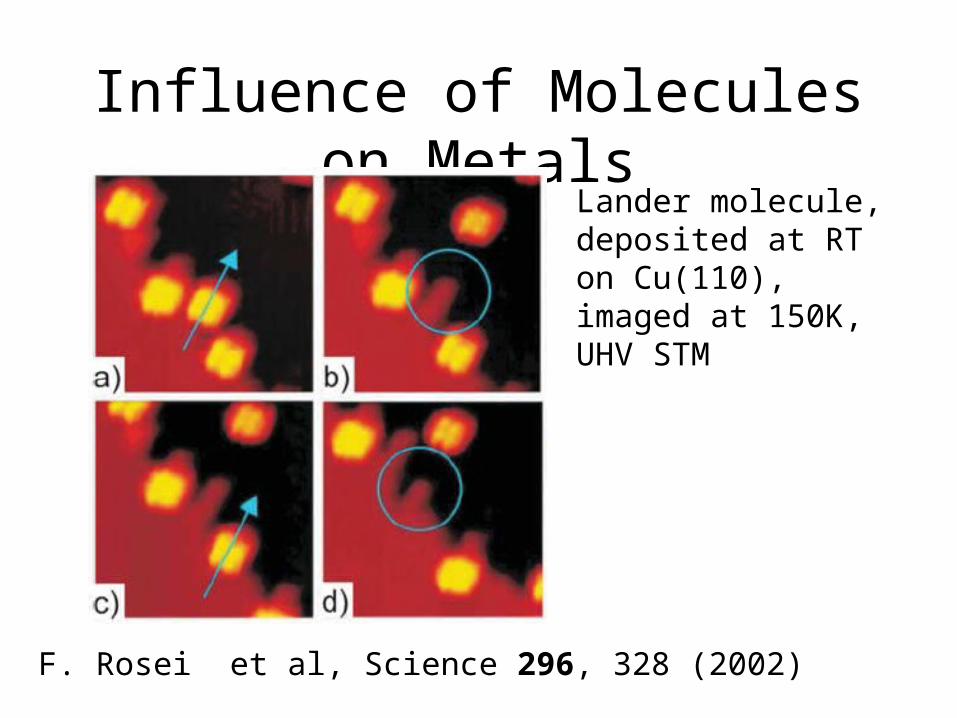
Influence of Molecules on Metals
F. Rosei et al, Science 296, 328 (2002)
Lander molecule, deposited at RT on Cu(110), imaged at 150K, UHV STM
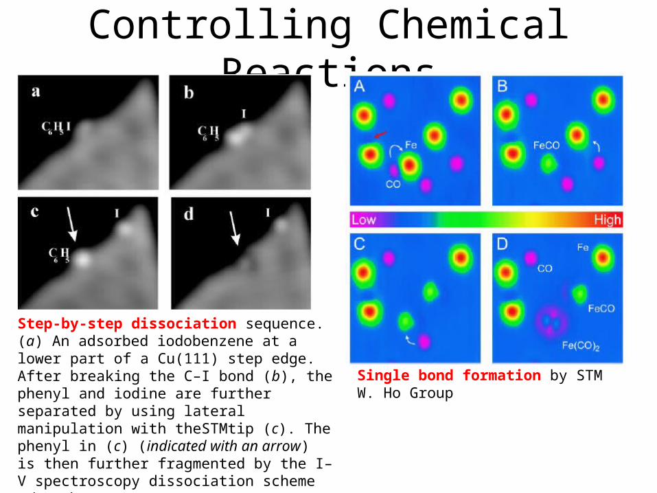
Controlling Chemical Reactions
Step-by-step dissociation sequence. (a) An adsorbed iodobenzene at a lower part of a Cu(111) step edge. After breaking the C–I bond (b), the phenyl and iodine are further separated by using lateral manipulation with theSTMtip (c). The phenyl in (c) (indicated with an arrow) is then further fragmented by the I–V spectroscopy dissociation scheme (d). Theresultant fragments include protrusion and depression regions contributed by the resulting hydrocarbon fragments. (Rieder Group, Berlin)
Single bond formation by STMW. Ho Group

an atomic switch!
Reliable for Xe, benzene, not so for Pt.
No current or electrical field neccessary.
2.2 Transfer or Near Contact
D. Eigler et al, Nature 352, 600 (1991)
J. Repp,
Rieder Group, Berlin
G. Meyer et al., Single Mol. 1, 79 (2000)
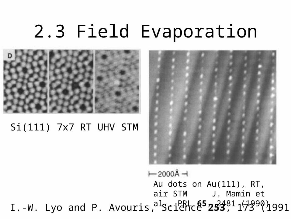
2.3 Field Evaporation
I.-W. Lyo and P. Avouris, Science 253, 173 (1991)
Si(111) 7x7 RT UHV STM
Au dots on Au(111), RT, air STM J. Mamin et al., PRL 65, 2481 (1990)
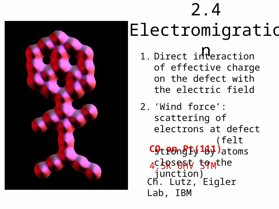
2.4 Electromigration
CO on Pt(111)
4.5K UHV STM
Ch. Lutz, Eigler Lab, IBM
1. Direct interaction of effective charge on the defect with the electric field
2. ‘Wind force’: scattering of electrons at defect (felt strongly by atoms closest to the junction)
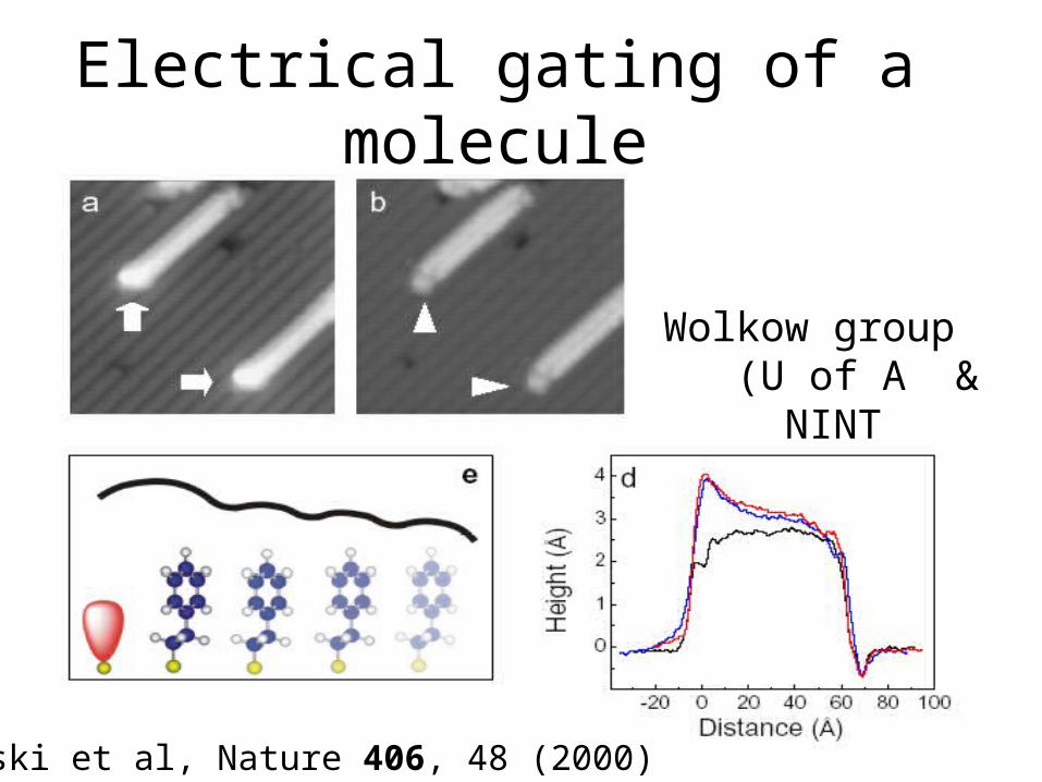
Electrical gating of a molecule
Wolkow group (U of A & NINT
Lopinski et al, Nature 406, 48 (2000)
Challenges
• Identification of manipulation mechanism
• Correlation with simulation and theory
• Identification of different building blocks
• 3D strutures
• Interfacing to the macroscopic world
x23
x60
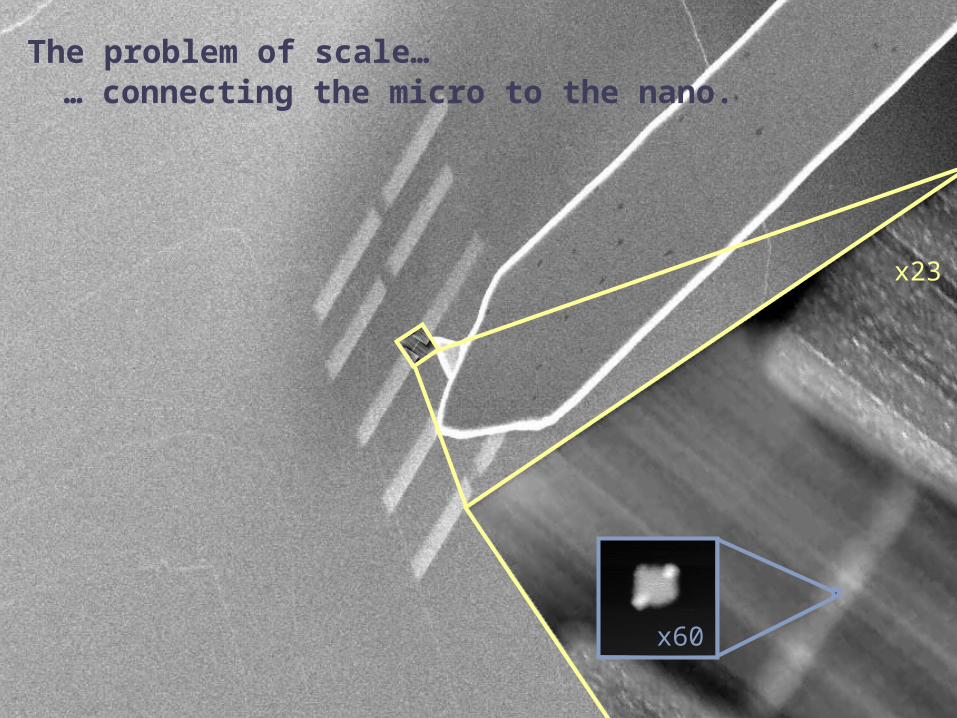
The problem of scale…… connecting the micro to the nano.