at89rfd-10 / evlb002 non-dimmable fluorescent ballast user
TRANSCRIPT
AT89RFD-10 / EVLB002 Non-Dimmable Fluorescent Ballast..........................................................................................................................................................
User Guide
Section 1Introduction ........................................................................................... 1-1
1.1 General Description .................................................................................1-21.2 Ballast Demonstrator Features ................................................................1-2
Section 2Ballast Demonstrator Device Features ................................................ 2-5
2.1 Atmel Supported Products .......................................................................2-52.2 IXYS Supported Products ........................................................................2-5
Section 3Ballast Description ............................................................................... 3-7
3.1 Circuit Topology .......................................................................................3-7
3.1.1 Line Conditioning ...............................................................................3-7
3.1.2 Low Voltage Supply ...........................................................................3-7
3.1.3 PFC Boost Regulator .........................................................................3-8
3.1.4 PFC Magnetics ..................................................................................3-8
3.1.5 Lamp Drive ........................................................................................3-8
3.1.6 Control ...............................................................................................3-8
3.1.7 IXYS IXI859 Charge Pump Regulator ...............................................3-9
3.1.8 IXYS IXTP02N50D Depletion Mode MOSFET used ..........................3-9
3.1.9 IXYS IXD611 Half bridge MOSFET driver .......................................3-10
3.1.10 IXYS IXTP3N50P PolarHV N-Channel Power MOSFET .................3-10
Section 4Circuit Operation................................................................................. 4-11
4.1 PFC ........................................................................................................4-11
4.1.1 PFC Sequence ................................................................................4-12
4.2 Lamp Circuit ...........................................................................................4-12
4.2.1 General ............................................................................................4-12
Section 5AT8xEB5114 Non-dimmable Software ............................................... 5-15
5.1 Main_AT8xEB5114_fluo_demo.c ..........................................................5-17
5.1.1 ADC STATE MACHINE ...................................................................5-17
5.2 Pfc_ctrl.c ................................................................................................5-19
5.2.1 PFC STATE MACHINE ...................................................................5-19
5.3.1 Lamp State Machine ........................................................................5-21
Section 6Conclusion ......................................................................................... 6-23
Ballast Demonstrator User Guide -1
7629A–AVR–04/06

6.1 Appendix 1: Capacitor Coupled Low Voltage Supply .............................6-236.2 Appendix 2: PFC Basics .........................................................................6-246.3 Appendix 3: Bill of Materials....................................................................6-256.4 Appendix 4: Schematic ...........................................................................6-28
-2 Ballast Demonstrator User Guide
7629A–AVR–04/06
Section 1Introduction
Efficient fluorescent lamps and magnetic ballasts have been the standard lighting fixturein commercial and industrial lighting for many years. Several lamp types, rapid start,high output, and others are available for cost effective and special applications. Thisuser guide covers operation and development details of the non-dimmable version ofour fluorescent ballast for operating a variety of lamps that are available today. Thisguide also covers power electronic circuits that find wide utilization in other applicationsbeyond lighting alone, which include Power Factor Correction, Half-Bridge InverterDrives, and Charge Pump Regulators all employing a variety of IXYS / Atmel parts.
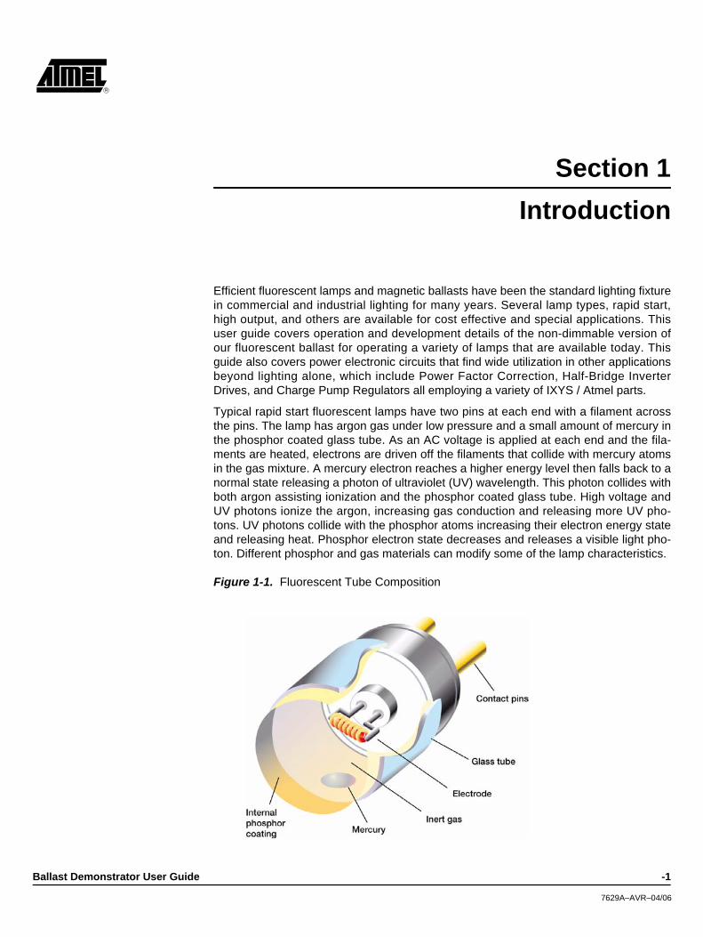
Typical rapid start fluorescent lamps have two pins at each end with a filament acrossthe pins. The lamp has argon gas under low pressure and a small amount of mercury inthe phosphor coated glass tube. As an AC voltage is applied at each end and the fila-ments are heated, electrons are driven off the filaments that collide with mercury atomsin the gas mixture. A mercury electron reaches a higher energy level then falls back to anormal state releasing a photon of ultraviolet (UV) wavelength. This photon collides withboth argon assisting ionization and the phosphor coated glass tube. High voltage andUV photons ionize the argon, increasing gas conduction and releasing more UV pho-tons. UV photons collide with the phosphor atoms increasing their electron energy stateand releasing heat. Phosphor electron state decreases and releases a visible light pho-ton. Different phosphor and gas materials can modify some of the lamp characteristics.
Figure 1-1. Fluorescent Tube Composition
Ballast Demonstrator User Guide -1
7629A–AVR–04/06
Since the argon conductivity increases and resistance across the lamp ends decreasesas the gas becomes excited, an inductance (ballast) must be used to limit and controlthe gas current. In the past, an inductor could be designed to limit the current for a nar-row range of mains voltage and frequency. A better method to control gas current is tovary an inductor's volt-seconds to achieve the desired lamp current and intensity. A vari-able frequency inverter operating from a DC bus can do this. If the inductor is part of anR-L-C circuit, rapid start ignition and operating currents are easily controlled dependingon the driving frequency versus resonant frequency.
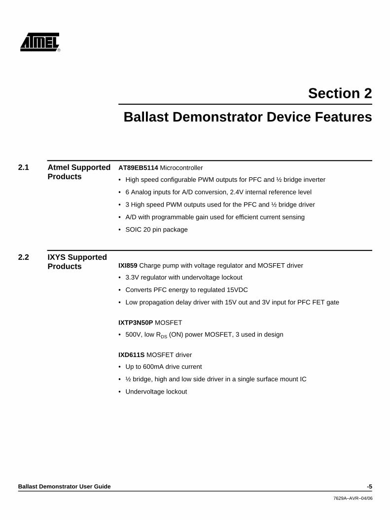
Utility is enhanced by designing a power factor correcting boost converter (PFC) toachieve the inverter DC bus over a wide mains voltage range of 90 - 265VAC, 50/60 Hz.Since a PFC circuit keeps the mains current and voltage in phase with very low distor-tion, mains power integrity is maintained. Additional utility is achieved by designing amicrocontroller for the electronic ballast application that can precisely and efficientlycontrol power levels in the fluorescent lamp. An application specific microcontrolleroffers the designer unlimited opportunity to enhance marketability of lighting products.The final design topology is shown in the block diagram of Figure 1-3.
1.1 General Description
Fluorescent ballast topology usually includes line conditioning for CE compliance, apower factor correction block including a boost converter to 380 V for universal inputapplications and a half bridge inverter. Varying the frequency of the inverter permits timefor filament preheat and ignition for rapid starting, including precise power control. Asshown in the block diagram, figure 3, all of these functions can be timed, regulated, anddiagnosed with the Atmel AT89EB5114 microcontroller.
1.2 Ballast Demonstrator Features
• Automatic microcontroller non-dimmable ballast
• Universal input _ 90 to 265 VAC 50/60 Hz, 90 to 370 VDC
• Power Factor Corrected (PFC) boost regulator
• Power feedback for stable operation over line voltage range
• Variable frequency half bridge inverter
• 18W, up to 2 type T8 lamps
• Automatic single lamp operation
-2 Ballast Demonstrator User Guide
7629A–AVR–04/06
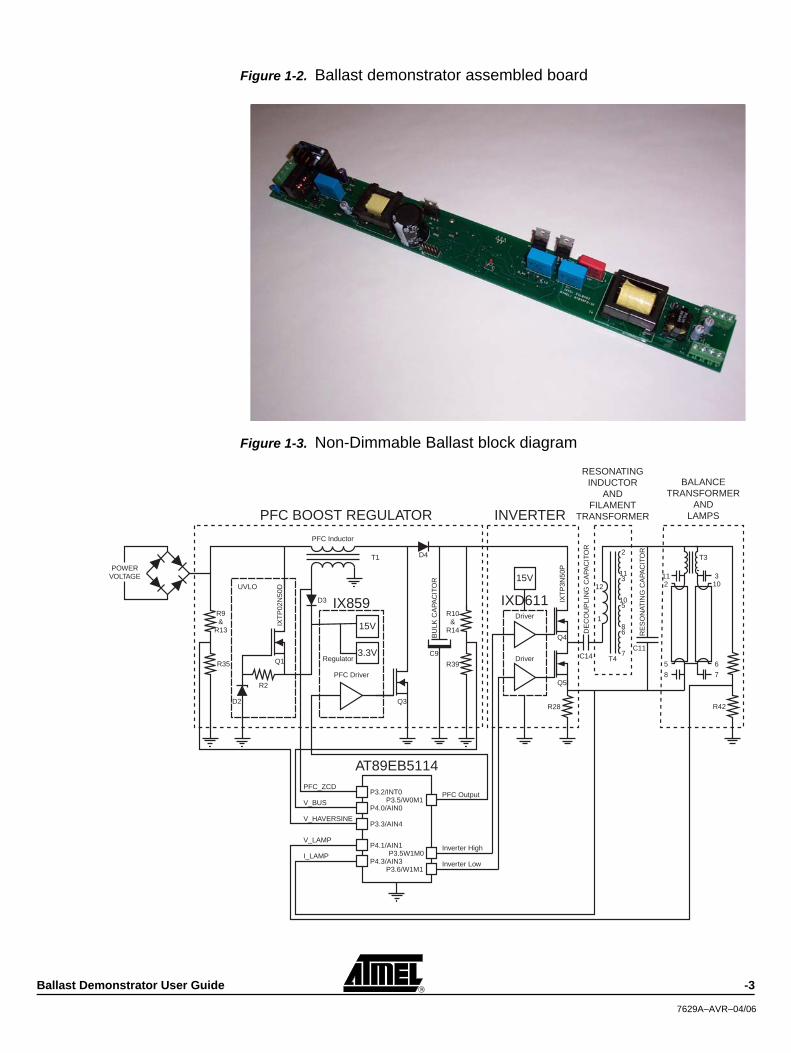
Figure 1-2. Ballast demonstrator assembled board
Figure 1-3. Non-Dimmable Ballast block diagram
UVLO
15V
3.3VRegulator
PFC Driver
IX859
PFC BOOST REGULATOR
Driver
Driver
15V
INVERTER
DE
CO
UP
LIN
G C
APA
CIT
OR
RESONATINGINDUCTOR
ANDFILAMENT
TRANSFORMER
2
113
105
86
7T4
IXD611
R28
IXT
P3N
50P
Q5
Q4BU
LK C
APA
CIT
OR
C9 C14
D4
Q3
R2
Q1
D2
D3
R9&
R13
R35
T1
IXT
P02
N50
D
R10&
R14
R39
112 10
3
5 6
7
C11R
ES
ON
ATIN
G C
APA
CIT
OR
T3
BALANCETRANSFORMER
ANDLAMPS
POWERVOLTAGE
R42
PFC Output
Inverter High
Inverter Low
V_HAVERSINE
V_BUS
V_LAMP
I_LAMP
P3.5/W0M1
P3.5W1M0
P3.6/W1M1
P4.0/AIN0
P3.3/AIN4
P4.1/AIN1
P4.3/AIN3
PFC_ZCDP3.2/INT0
AT89EB5114
8
12
1
PFC Inductor
Ballast Demonstrator User Guide -3
7629A–AVR–04/06
Section 2Ballast Demonstrator Device Features
2.1 Atmel Supported Products
AT89EB5114 Microcontroller
• High speed configurable PWM outputs for PFC and ½ bridge inverter
• 6 Analog inputs for A/D conversion, 2.4V internal reference level
• 3 High speed PWM outputs used for the PFC and ½ bridge driver
• A/D with programmable gain used for efficient current sensing
• SOIC 20 pin package
2.2 IXYS Supported Products IXI859 Charge pump with voltage regulator and MOSFET driver
• 3.3V regulator with undervoltage lockout
• Converts PFC energy to regulated 15VDC
• Low propagation delay driver with 15V out and 3V input for PFC FET gate
IXTP3N50P MOSFET
• 500V, low RDS (ON) power MOSFET, 3 used in design
IXD611S MOSFET driver
• Up to 600mA drive current
• ½ bridge, high and low side driver in a single surface mount IC
• Undervoltage lockout
Ballast Demonstrator User Guide -5
7629A–AVR–04/06
Section 3Ballast Description
3.1 Circuit Topology • Line conditioning with input filter and varistor for noise suppression and protection.
• Low Voltage supply
• PFC / boost regulator
• PFC magnetics
• Lamp drive
• Microprocessor control
• Charge pump regulator
• ½ bridge driver
• ½ bridge power MOSFET stage for up to 2 lamps
3.1.1 Line Conditioning An input filter section consisting of C1, C3, and common mode choke L1 prevent switch-ing signal frequencies and their harmonics from the PFC boost converter from beingconducted to the mains. Varistor RV1 protects the ballast circuit from line voltage tran-sients. Full wave bridge rectifier BR1 converts the line AC to a DC haversine. Diode D2is used to provide a point ahead of the boost inductor and filter where the haversine sig-nal can be sensed by the microcontroller. This is necessary for the proper timing of thePFC control drive signal which must maintain a constant ON time pulse width over ahaversine period.
3.1.2 Low Voltage Supply 3.3V microcontroller power and ~ 15V FET drive power are provided by the low voltagesupply consisting of a current source (Q1) and multipurpose IC U1 (IXI589). Internal toU1 are a 3.3V linear regulator, a 15V (nominal) two point regulator, under-voltage lock-out comparators and control, charge pump switching circuitry, and a FET driver. (Seemore detailed description of the IXI859 below) For startup, the current source formed byQ1, and its associated components sources current into C6 until the voltage at U1 pin 1reaches the under-voltage lockout upper limit of approximately 14.1V. The currentsource voltage output is limited by zener diode D3 to about 16 V. When the under-volt-age lockout limit is reached, the IXI859 begins to supply 3.3V to the microcontroller. Themicrocontroller then begins to supply drive pulses to the PFC FET Q3 through theIXI859 FET gate driver. The charge pump regulator circuit is then able to supply 15Vpower by efficiently converting energy from the PFC switching circuit. This feature is notused in the non-dimmable demonstrator design. Rather, a voltage doubler circuit con-sisting of D4, D20 and C31 connected to the PFC transformer secondary provides 15Vpower after startup.
Ballast Demonstrator User Guide -7
7629A–AVR–04/06

3.1.3 PFC Boost Regulator
The PFC (Power Factor Correcting) boost regulator circuit is used to convert the recti-fied input line voltage to a 380V DC supply while maintaining a sinusoidal average inputcurrent in phase with the input voltage. The microcontroller accomplishes this by switch-ing the PFC FET with ON times that are constant over a haversine period and bymaintaining nearly critical conduction conditions. Since the current in the PFC inductoris nearly triangular and its peaks are proportional to the input haversine voltage, theaverage current is proportional to the input waveform. Therefore, the power factor ismaintained near unity.
3.1.4 PFC Magnetics Without going into the derivations of the formulas used, the transformer design is asfollows:
L = [(1.4 * 90VAC) * (20 uS)] / 3.6A peak = 700 uH
A 3.6 Apk maximum FET current is 1.8 A approximately divided by the ON/OFF ratio.The ON time has been discussed earlier and the OFF time maximum will occur at highline condition at the peak of the haversine. A 16 mm core was chosen for the recom-mended power density at 200 mT and 50 KHz.
3.1.5 Lamp Drive The microcontroller sends rectangular pulses to the half-bridge driver (IXD611). TheIXD611 contains high side and low side FET drivers and floating high side supply cir-cuitry to produce high side gate drive. (See more detailed description of the IXD611 tofollow) The pulses from the microcontroller are non-overlapping and 180 degrees out ofphase. A deadband time between HBRIDGE HI and HBRIDGE LO pulses insures thatboth drivers are never on at the same time. The lamp drive is constant in duty cycle. Thepower to the lamps is controlled by varying the frequency of the drive signals. TheIXD611 drives two FETs (IXTP3N50P) in a half-bridge configuration.
The output of the half-bridge is AC coupled by C11 to the lamps through a resonatingtransformer and capacitor (T4 and C12). Additional windings on T4 supply filament cur-rent to the lamps. Balance transformer T3 forces the current to be shared equally by thetwo lamps. The lamp currents are conducted to circuit common through a 1 Ohm resis-tor which is used to sense the lamp current so that lamp power may be controlled by themicrocontroller.
3.1.6 Control The ballast is controlled by microcontroller U3. U3 is an Atmel AT8xEB5114 with an80C51 core and specialized circuitry for controlling the ballast. Included are two PWMunits that are used for controlling the PFC drive and the half-bridge drive with deadtime.An internal analog to digital converter converts input signals so the processor can moni-tor and control the ballast.
The AT8xEB5114 pin connections for ballast control and scale factors for analog inputsare as follows:
• P4.0/AIN0 VBus monitor input (VBus = AIN0 x 201)
• P4.1/AIN1 Rectified Lamp Voltage Sense (Vlamp = AIN1 x 294)
• P4.2/AIN2 Lamp AC Voltage (VAC ~= AIN2 x 446)
• P4.3/AIN3 Lamp Current (Amplify by 10) (Ilamp = AIN3/1Ohm)
• P3.3/AIN4 Haversine Voltage input (Vhaversine = AIN4 x 201)
• P3.4/AIN5 Temperature sensor (Vtemp = 1.1V @ 25C || .264V @ 85C)
• P3.6 NC (No Connection)
• P3.5/W1M0 PFC Drive
• P3.2/INT0 Current Zero Crossing Detect (Interrupt)
• P3.1/W0M1 Half Bridge high side drive
-8 Ballast Demonstrator User Guide
7629A–AVR–04/06
• P3.0/W0M0 Half Bridge low side drive
The Temperature monitor is a thermistor with a nominal 10K resistance at 25°C and1.74K resistance at 80°C. It is mounted on the circuit board and so monitors ambienttemperature in the lamp housing.
Additional dedicated pins allow in-circuit programming of the flash memory using headerJ2. Other pins provide connections for the oscillator and voltage reference components.
3.1.7 IXYS IXI859 Charge Pump Regulator
The IXI859 charge pump regulator integrates three primary functions central to the PFCstage of the ballast demonstrator. First it includes a linear regulated supply voltage out-put, and in this application the linear regulator provides 3.3V to run the microcontroller.The second function is a gate drive buffer that switches an external power MOSFETused to boost the PFC voltage to 380V. Once the microcontroller is booted up and run-ning, it generates the input signal to drive the PFC MOSFET through the IXI859 gatedrive buffer. Finally, the third function provides two point regulated supply voltage foroperating external devices. As a safety feature, the IXI859 includes an internal Vccclamp to prevent damage to itself due to over-voltage conditions.
In general applications at start-up, an R-C combination is employed at the Vcc supplypin that ramps up a trickle voltage to the Vcc pin from a high voltage offline source. Thevalue of R is large to protect the internal zener diode clamp and as a result, can't supplyenough current to power the microcontroller on it's own. C provides energy to boot themicrocontroller. At a certain voltage level during the ramp up, the Under Voltage LockOut point is reached and the IXI859 enables itself. The internal voltage regulator thatsupplies the microcontroller is also activated during this time. However, given the tricklecharge nature of the Vcc input voltage, the microcontroller must boot itself up andenable PFC operation to provide charge pump power to itself. This means that the R-Ccombination must be sized carefully so that the voltage present at the Vcc pin does notcollapse too quickly under load and causes the UVLO circuitry to disable device opera-tion before the microcontroller can take over the charge pump operation. There are acouple of problems associated with this method. Namely, under normal operation aspreviously mentioned, the internal zener diode clamps the input Vcc pin voltage and Rmust dissipate power as long as the zener diode is clamped. Assuming that a rectifiedsine wave is supplied at the Vcc means that the internal zener will be clamped and R willbe dissipating power as long as the input voltage is greater than the zener voltage.Another problem is that when a universal range is used at the Vcc pin, 90-265V, R mustdissipate nine times the power, current squared function for power in R, over a three-fold increase of voltage from 90V at the low end to 265V on the high end.
As an alternative and as used in the ballast demonstrator, the Vcc pin is fed voltage byway of a constant current source. This circuit brings several advantages over the regularR-C usage. First we can reduce power consumed previously by R and replace it with acircuit that can provide power at startup and once the microcontroller is running, shut offcurrent into the Vcc pin. The constant current source also has the ability to provide suffi-cient power to run the microcontroller unlike the R-C combination. This would be anadvantage in the case that a standby mode is desired. Overall power consumption canbe reduced by allowing the microcontroller to enter a low power mode and shut downPFC operation without having to reboot the microcontroller. Since the R-C combinationcannot provide enough power to sustain microcontroller operation, the microcontrollermust stay active running the PFC section to power itself.
3.1.8 IXYS IXTP02N50D Depletion Mode MOSFET used as a current source
The IXYS IXTP02N50D depletion mode MOSFET is used in this circuit to provide powerand a start-up voltage to the Vcc pin of the IXI859 charge pump regulator. TheIXTP02N50D acts as a current source and self regulates as the source voltage risesabove the 15V zener voltage and causes the gate to become more negative than the
Ballast Demonstrator User Guide -9
7629A–AVR–04/06
source due to the voltage drop across the source resistor. Enough energy is availablefrom the current source circuit during the conduction angles to keep the IXI859 (U1) pin1 greater than 14VDC as required to enable the Under Voltage Lock Out (UVLO) cir-cuitry in the IXI859.
3.1.9 IXYS IXD611 Half bridge MOSFET driver
The IXD611 half bridge driver includes two independent high speed drivers capable of600mA drive current at a supply voltage of 15V. The isolated high side driver can with-stand up to 650V on its output while maintaining its supply voltage through a bootstrapdiode configuration. In this ballast application, the IXD611 is used in a half-bridgeinverter circuit driving two IXYS IXTP3N50P power MOSFETs. The inverter load con-sists of a series resonant inductor and capacitor to power the lamps. Filament power isalso provided by the load circuit and is wound on the same core as the resonant induc-tor. Pulse width modulation (PWM) is not used in this application, instead the power iscontrolled through frequency variation. It is important to note that pulse overlap, whichcould lead to the destruction of the two MOSFETs due to current shoot through, is pre-vented via the input drive signals through the microcontroller. This parameter, alsoknown as dead time, is not available on this particular driver. However, a dead timeoption is built in on other driver models within the IXYS bridge driver family.
Other features of the IXD611 driver include: – Wide supply voltage operation 10-35V – Matched propagation delay for both drivers – Undervoltage lockout protection – Latch up protected over entire operating range
• +/- 50V/ns dV/dt immunity
3.1.10 IXYS IXTP3N50P PolarHV N-Channel Power MOSFET
The IXTP3N50P is a 3A 500V general purpose power MOSFET that comes from thefamily of IXYS PolarHV MOSFETs. When comparing equivalent die sizes, PolarHTresults in 50% lower R DS(ON), 40% lower R THJC (thermal resistance, junction tocase), and 30% lower Qg (gate charge) enabling a 30% - 40% die shrink, with the sameor better performance verses the 1st generation power MOSFETs.
Within the ballast demonstrator itself the IXTP3N50 serves two functions. The first ofwhich is the power switching pair of devices in the half-bridge circuit that drives thelamps. While a third device serves duty in the main PFC circuit as the power switch thatdrives the PFC inductor.
-10 Ballast Demonstrator User Guide
7629A–AVR–04/06
Section 4Circuit Operation
General requirements
• One or two lamps, type T8 of any characteristics
– Ballast to compensate automatically – Hardware is capable of up to 40W per lamp
• Line voltage of 90 to 265 VAC, 50 or 60 Hz
– 380 volt DC bus as provided by a power factor correcting boost regulator(PFC)
4.1 PFC Upon application of mains power, without the PFC running, the filter cap C9 will chargeto the peak line voltage. The current source will supply the low voltages. After the DCbus voltage is 0.9 times the haversine peak and the under voltage lockout (UVLO)requirements are met, a series of fixed width soft-start pulses are sent to the PFC FETof 10 uS at a 20 KHz rate. At very low 380V load current the 380DVC bus should rise to380V. If the bus rises to 410 VDC, all PFC pulses stop. The zero crossing detector(P3.2/INT0) starts to sense zero crossings from the PFC transformer secondary. A 380VDC bus and a zero crossing event starts the PFC control loop.
Checks are made for the presence of the rectified mains (haversine) and bus voltagethroughout normal operation. Mains sense (P3.3/AIN4) < 0.76 V pk (90 VAC) or > 2.24V pk (265 VAC) faults the PFC to off, turns off the ½ bridge and initiates a restart.
The control consists of measuring the 380V bus error from the 380V setpoint of 1.89 Vat P4.0/AIN0 to determine the PFC drive pulse width (PW). The PW is made propor-tional to the error, and has to be constant during a complete half period, so the update isdone each time the haversine is null. A maximum PW limit should be coded to limit theFET current under upset of high error and high haversine (265VAC*1.4). The maximumpulse width allowed is inversely proportional to the peak haversine voltage and variesbetween 6 uS at high line and 20 uS at low line.
PWmax = K/Vhaversine
Current sensing of the PFC FET source is not needed as the peak current allowed canbe set by the haversine peak detect.
tmax = L Ipk / Vhaversine
With L at 700 uH and Ipk at 3.2 A, tmax = 6 uS at high line (265 Vrms). This also effec-tively limits the FET dissipation under upset conditions. Under normal operation, a pulse
Ballast Demonstrator User Guide -11
7629A–AVR–04/06
width maximum of 20 uS is allowed for maximum 380 VDC error but with the high linelimitation. 1% regulation of the 380 VDC bus was achieved with this control scheme.
After the PFC FET ON pulse, the PFC inductor flyback boosts the voltage through D6 tothe bulk filter capacitor. The boost current decays as measured by the inductor second-ary. After the current goes to zero, the next pulse is started. This ensures operation innear critical conduction boost mode. The current zero crossing detect of P3.2/INT0 setsthe PFC off time. This off time is effectively proportional to the haversine amplitude withthe lowest PFC frequency occurring at the haversine crest and the highest frequency atthe haversine zero. Because of the haversine voltage, and di=v*dt/L the mains currentenvelope should follow the voltage for near unity power factor. This assumes a nearlyconstant error (di) of the 380 VDC bus over each haversine period.
The PFC on time is modified proportionally to the error between 380V and the actualvalue of the 380VDC BUS. In case the Vbus reaches the overshoot value (410V) thepulse is reduce to 0.
4.1.1 PFC Sequence 1. Power on. 2. IXI859 function block supplies 3.3V to microcontroller 3. Microcontroller undervoltage lockout released 4. Disable half-bridge drive output 5. Disable P3.2/INT0 comparator. 6. P3.3/AIN4 must be >0.76 Vmin (90VAC) & <2.24 (265VAC) Vmax (haversine
peak) for the PFC to start. 7. Check AC line condition every 200 mS maximum (10 cycles of 50 Hz). 8. If fail check, halt PFC, and Half-Bridge. Do not restart until line within specs to
protect PFC. 9. Soft start PFC with 10 uS pulses at 50 uS period for 800 uS. 10. Monitor for a zero crossing of the PFC inductor secondary voltage. This occurs
after the 10 uS start pulse burst. 11. If no Zero Crossing & after 800 uS halt PFC Drive, wait 1 second & provide PFC
Drive with 10 uS pulses for 800 uS. Try 10 times 12. After Zero Crossing and 380 VDC (1.89 V at P4.0/AIN0) enable PFC control loop 13. If > 410V (2.04 V at P4.0/AIN0) then inhibit PD0 pulse 14. If < 380V (1.89 V at P4.0/AIN0) then use the control loop to establish the pulse
width. 15. Limit pulse width to 25 uS or as determined by the haversine peak voltage. 16. After PFC pulse, wait until Zero Crossing detected (PFC off time) then enable
PFC pulse with width calculated from bus error and haversine peak.
4.2 Lamp Circuit
4.2.1 General T4 primary and C12 form a series resonant circuit driven by the output half bridge. Sincethe output is 380V pulsed DC, DC isolation is provided by C11 to drive the lamp circuitwith AC. The lamp is placed across the resonating capacitor C12. The lamp filamentsare driven by windings on T4 secondaries to about 3 Vrms so that the resonating induc-tor current provides the starting lamp filament current.
Sequentially, the lamp is started at a frequency well above resonance at 100 KHz beforeramping down to 55 KHz ignition. 80 KHz provides a lagging power factor where most of
-12 Ballast Demonstrator User Guide
7629A–AVR–04/06
the drive voltage appears across the inductor. A smaller voltage appears across the res-onating capacitor and the lamps. However with 1 mH gapped inductance, there issufficient inductor current to power the filaments.
For lamp ignition, the frequency is reduced from 80 KHz to 40 KHz at 30 KHz/sectowards resonance causing the lamp voltage to rise to about 340 Vpeak.
Ignition occurs at about 40 KHz for a 18W T8 lamp. The plasma established in the lamppresents a resistive load across the resonating capacitor thereby reducing the voltageacross the capacitor and shifting the reactive power in the bridge circuit to resistivepower in the lamp.
A further reduction in frequency to 32 KHz at 30 KHz/sec establishes maximum bright-ness as the resonant circuit now has a leading (capacitive) power factor causing morevoltage and current (approx. 360 Vpeak) across the capacitor and the lamp.
4.2.1.1 Single lamp operation
Single lamp operation can be detected from the 380VDC bus current through the 1 Ohmsense resistor. At preheat the current for one lamp is half that for two lamps. This cur-rent is also used to sense open filament condition or lamp removed under powercondition. An abrupt change in the bus current is a good indicator of lamp condition thatdoes not require a high frequency response nor a minimal response due to reactivecurrents.
Once single lamp condition is detected, the minimum run frequency is determined byIx380V = Single Lamp Power. If the single lamp condition occurs during "run" as notedby a decrease in current of more than 20% from the preset level, increase the frequencyuntil the single lamp power conditions are met. If the current increases by more than20% , assume the lamp has been replaced. Step Increase the frequency to 80 KHz torestart the ignition process. This is necessary to preheat the new lamp filament toensure that the hot lamp will not ignite much sooner than the cold lamp exceeding thebalance transformer range.
Repeat ignition sequence. With one cold lamp in parallel with one hot lamp, it may benecessary to restart several times to get both lamps to ignite.
The AT8xEB5114 internal amplifier has the gain preset in the program to 10. This scalesthe lamp current input to a reasonable A/D resolution.
4.2.1.2 Lamp Number Sequence
After Vbus = 380 V start preheat
Start half-bridge drive with 12.5 uS total period (80 KHz)
If I > 20 ma, then 2 lamps. If I < 20 ma assume a single lamp.
I < 10 ma assume an empty fixture = fault & shutdown.
4.2.1.3 Start Ignition Sequence
1. Sweep half-bridge frequency down at 30 KHz/sec 2. Stop sweep at 40 KHz or 25 uS period (12.5 uS pulses for each ½ bridge FET) 3. Check I > 100 ma (2 lamps) or > 30 ma (1 lamp) for proof of ignition 4. Hold ignition frequency for 10 mS 5. Measure the lamp voltage collapse for proof of ignition (P4.1/AIN1 < 200 mV) 6. If the lamp voltage has not collapsed, increase frequency to 77 KHz for preheat
for 1 second. Repeat ignition sequence. 7. Proceed to full power setting at 30 KHz/sec rate after ignition is detected.
4.2.1.4 Power Control Calculate input power for both lamps = I x 380VDC.
Adjust freq. up (lower power) or down (higher power) at 30 KHz/sec rate.
Limit freq. to 32 KHz to 80 KHz range.
Ballast Demonstrator User Guide -13
7629A–AVR–04/06

If lamp currents exceed power limits by 10% (as determined by lamp type), set half-bridge drive off due to over current. Start re-ignition sequence. Repeat 6 times and if stillout of spec, shutdown PFC and half-bridge drive.
PD6 rectified AC drive
Checks are made for the presence of the rectified mains (haversine) and bus voltagethroughout normal operation. Mains voltage < 90 VAC or 265 VAC peak faults the PFCto off, turns off the half-bridge and initiates a restart.
-14 Ballast Demonstrator User Guide
7629A–AVR–04/06

Section 5AT8xEB5114 Non-dimmable Software
This section of the document describes the software architecture utilizing the followingsource code files and related state machines.
Main_at8xeb5114_fluo_demo.c – ADC State Machine
Pfc_ctrl.c – PFC State Machine
Lamp_ctrl.c – Lamp State Machine
And their associated header files.
- main_at8xeb5114_fluo_demo.h – Pfc_ctrl.h – Lamp_ctrl.h
Including the following peripherals:
• TIMER0, ADC, amplifier, PWM0, and PWM1.
In order for the ballast to operate, there are two primary control systems that run simul-taneously. The first is for the PFC control and second for the Lamp control.
Furthermore in order to work properly, the state machines require input data. This ana-log data is provided via an auto running interrupt mode ADC state machine.
The complete software package for the application is split into the functional blocks inthe diagram shown below. While the variables are identified as follows.
• g_ global
• gv_global volatile
• gs_ global static
Voltage and current variables are identified by the following examples
• g_v or g_i global - voltage/current
• gv_v or gv_i global volatile - voltage/current
• gs_v or gs_i global static - voltage/current
Ballast Demonstrator User Guide -15
7629A–AVR–04/06
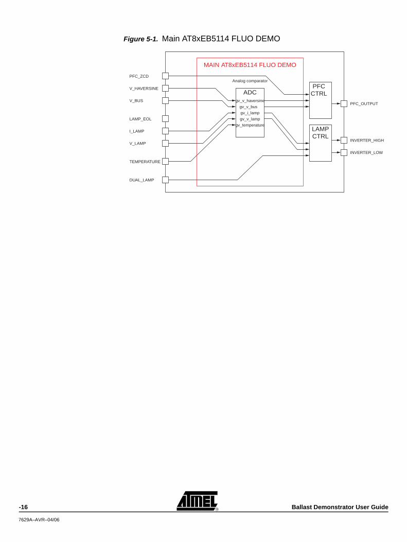
Figure 5-1. Main AT8xEB5114 FLUO DEMO
V_HAVERSINE
TEMPERATURE
I_LAMP
V_LAMP
V_BUS
PFC_ZCD
LAMP_EOL
Analog comparator
ADC
PFC_OUTPUT
INVERTER_HIGH
INVERTER_LOW
DUAL_LAMP
PFCCTRL
LAMPCTRL
gv_v_haversine
gv_v_bus
gv_i_lamp
gv_v_lamp
gv_temperature
MAIN AT8xEB5114 FLUO DEMO
-16 Ballast Demonstrator User Guide
7629A–AVR–04/06
5.1 Main_AT8xEB5114_fluo_demo.c
This file executes all the peripherals initializations and then schedules the different con-trol tasks.
The ADC state machine is included in this file. The ADC state machine is controlled viainterrupts.
5.1.1 ADC STATE MACHINE
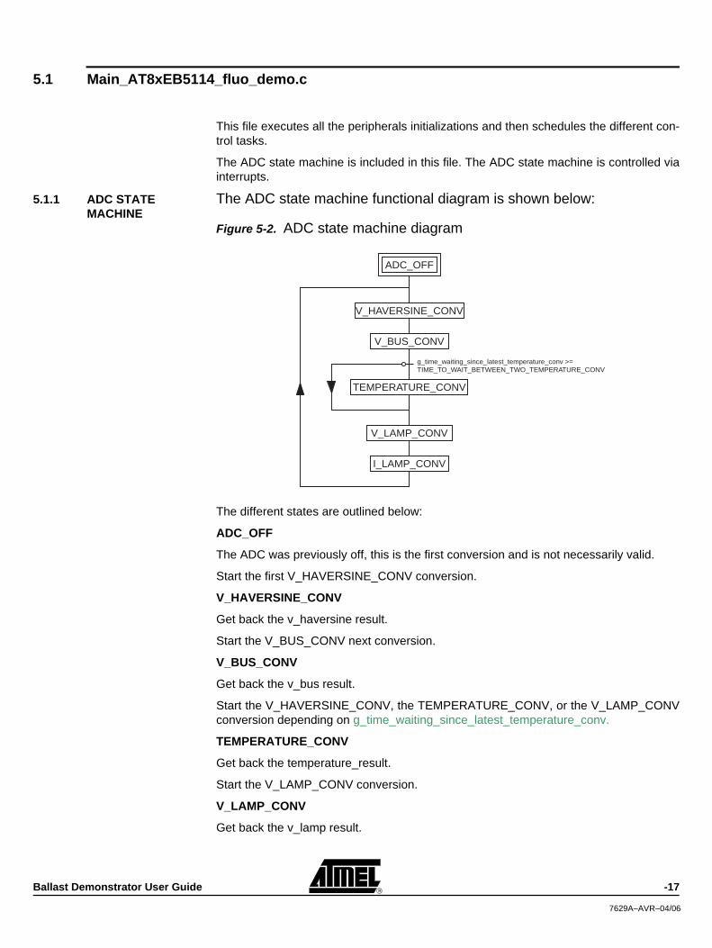
The ADC state machine functional diagram is shown below:
Figure 5-2. ADC state machine diagram
The different states are outlined below:
ADC_OFF
The ADC was previously off, this is the first conversion and is not necessarily valid.
Start the first V_HAVERSINE_CONV conversion.
V_HAVERSINE_CONV
Get back the v_haversine result.
Start the V_BUS_CONV next conversion.
V_BUS_CONV
Get back the v_bus result.
Start the V_HAVERSINE_CONV, the TEMPERATURE_CONV, or the V_LAMP_CONVconversion depending on g_time_waiting_since_latest_temperature_conv.
TEMPERATURE_CONV
Get back the temperature_result.
Start the V_LAMP_CONV conversion.
V_LAMP_CONV
Get back the v_lamp result.
V_HAVERSINE_CONV
TEMPERATURE_CONV
V_BUS_CONV
ADC_OFF
g_time_waiting_since_latest_temperature_conv >= TIME_TO_WAIT_BETWEEN_TWO_TEMPERATURE_CONV
V_LAMP_CONV
I_LAMP_CONV
Ballast Demonstrator User Guide -17
7629A–AVR–04/06

Start the I_LAMP_CONV conversion.
I_LAMP_CONV
Get back the i_lamp result.
Start the next conversion cycle with a V_HAVERSINE_CONV conversion.
-18 Ballast Demonstrator User Guide
7629A–AVR–04/06
5.2 Pfc_ctrl.c This fi le executes the PFC state machine according to the scheduler in theMain_AT8xEB5114_fluo_demo.c file.
5.2.1 PFC STATE MACHINE
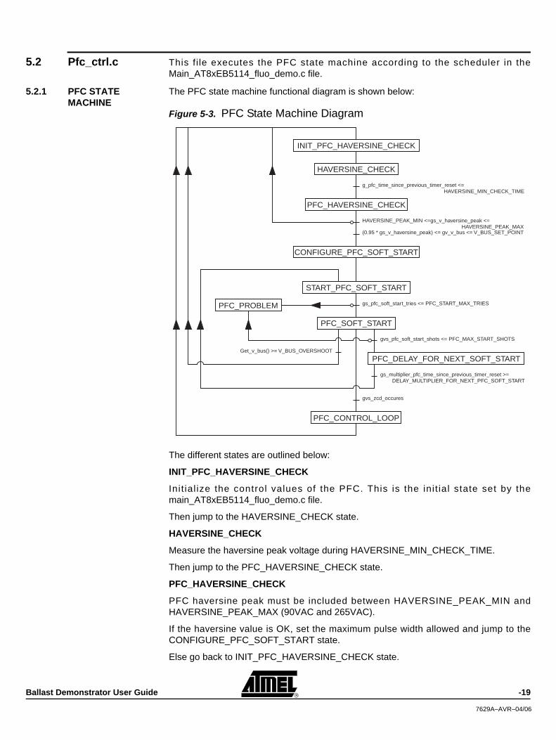
The PFC state machine functional diagram is shown below:
Figure 5-3. PFC State Machine Diagram
The different states are outlined below:
INIT_PFC_HAVERSINE_CHECK
Ini t ial ize the control values of the PFC. This is the init ial state set by themain_AT8xEB5114_fluo_demo.c file.
Then jump to the HAVERSINE_CHECK state.
HAVERSINE_CHECK
Measure the haversine peak voltage during HAVERSINE_MIN_CHECK_TIME.
Then jump to the PFC_HAVERSINE_CHECK state.
PFC_HAVERSINE_CHECK
PFC haversine peak must be included between HAVERSINE_PEAK_MIN andHAVERSINE_PEAK_MAX (90VAC and 265VAC).
If the haversine value is OK, set the maximum pulse width allowed and jump to theCONFIGURE_PFC_SOFT_START state.
Else go back to INIT_PFC_HAVERSINE_CHECK state.
INIT_PFC_HAVERSINE_CHECK
PFC_CONTROL_LOOP
PFC_DELAY_FOR_NEXT_SOFT_START
PFC_SOFT_START
START_PFC_SOFT_START
CONFIGURE_PFC_SOFT_START
HAVERSINE_CHECK
PFC_HAVERSINE_CHECK
g_pfc_time_since_previous_timer_reset <= HAVERSINE_MIN_CHECK_TIME
HAVERSINE_PEAK_MIN <=gs_v_haversine_peak <= HAVERSINE_PEAK_MAX(0.95 * gs_v_haversine_peak) <= gv_v_bus <= V_BUS_SET_POINT
gs_pfc_soft_start_tries <= PFC_START_MAX_TRIESPFC_PROBLEM
gvs_zcd_occures
Get_v_bus() >= V_BUS_OVERSHOOT
gvs_pfc_soft_start_shots <= PFC_MAX_START_SHOTS
gs_multiplier_pfc_time_since_previous_timer_reset >= DELAY_MULTIPLIER_FOR_NEXT_PFC_SOFT_START
Ballast Demonstrator User Guide -19
7629A–AVR–04/06

CONFIGURE_PFC_SOFT_START
Configures the peripherals PWM1 and interrupt 0 to soft start the PFC.
Then jump to START_PFC_SOFT_START.
START_PFC_SOFT_START
Check that the soft start has been tried less than PFC_START_MAX_TRIES
If OK then start PWM1 and jump to PFC_SOFT_START state.
Else immediately jump to PFC_PROBLEM state.
PFC_SOFT_START
The PFC soft start consists on PFC_MAX_START_SHOTS pulses configured onPFC_SOFT_START_CONFIGURATION.
If a zero crossing detection appears, jump to the PFC_CONTROL_LOOP state
Else go to INIT_PFC_HAVERSINE_CHECK, PFC_DELAY_FOR_NEXT_PFC_SOFT_START, or PFC_PROBLEM state depending on the different conditions detailed in the PFC diagram.
PFC_DELAY_FOR_NEXT_PFC_SOFT_START
In case the soft start fails, the software has to wait DELAY_FOR_NEXT_PFC_SOFT_START*DELAY_MULTIPLIER_FOR_NEXT_PFC_SOFT_START, before trying a new soft start by going back to the START_PFC_SOFT_START state.
PFC_CONTROL_LOOP
A zero crossing detection occurs so the PFC is now started and the PFC can be config-ured on autoretrigg mode. The PFC is now running. This is the normal PFC loop control.
-20 Ballast Demonstrator User Guide
7629A–AVR–04/06
5.3 Lamp_ctrl.c This f i le executes Lamp state machine according to the scheduler in theMain_AT8xEB5114_fluo_demo.c file.
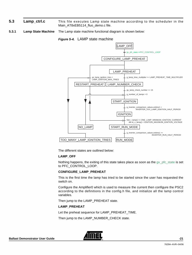
5.3.1 Lamp State Machine The Lamp state machine functional diagram is shown below:
Figure 5-4. LAMP state machine
The different states are outlined below:
LAMP_OFF
Nothing happens, the exiting of this state takes place as soon as the gv_pfc_state is setto PFC_CONTROL_LOOP.
CONFIGURE_LAMP_PREHEAT
This is the first time the lamp has tried to be started since the user has requested theswitch on.
Configure the Amplifier0 which is used to measure the current then configure the PSC2according to the definitions in the config.h file, and initialize all the lamp controlvariables.
Then jump to the LAMP_PREHEAT state.
LAMP_PREHEAT
Let the preheat sequence for LAMP_PREHEAT_TIME.
Then jump to the LAMP_NUMBER_CHECK state.
CONFIGURE_LAMP_PREHEAT
START_IGNITION
LAMP_PREHEAT
LAMP_NUMBER_CHECK
g_lamp_time_multiplier >= LAMP_PREHEAT_TIME_MULTIPLIER
gs_lamp_check_number >= 15
LAMP_OFF
gv_pfc_state==PFC_CONTROL_LOOP
g_inverter_comparison_values.ontime1 < INVERTER_XXX_LAMP_IGNITION_HALF_PERIOD
IGNITION
Get_i_lamp() >= ONE_LAMP_MINIMUM_IGNITION_CURRENT && et_v_lamp() < IGNITION_MAXIMUM_IGNITION_VOLTAGE
RESTART_PREHEAT
gs_lamp_ignition_tries < LAMP_IGNITION_MAX_TRIES
START_RUN_MODE
g_inverter_comparison_values.ontime1 >= INVERTER_RUN_HALF_PERIOD
RUN_MODE
g_number_of_lamps > 0
TOO_MANY_LAMP_IGNITION_TRIES
NO_LAMP
Ballast Demonstrator User Guide -21
7629A–AVR–04/06

LAMP_NUMBER_CHECK
Check the preheat current in order to know whether there is one or two lamps
Then jump to the START_IGNITION state.
In case there is no lamp, jump to the NO_LAMP state.
START_IGNITION
Decrease the frequency from the init frequency down to INVERTER_IGNITION_HALF_PERIOD.
Then jump to IGNITION state.
IGNITION
The ignition sequence consists in maintaining the ignition frequency determined byINVERTER_IGNITION_HALF_PERIOD for 10ms, then checking for ignition by measur-ing lamp current and voltage.
In case it is... START_RUN_MODE.
In case it isn't... RESTART_PREHEAT.
RESTART_PREHEAT
Reconfigure the Inverter with the Restart parameters, then LAMP_PREHEAT.
If Ignition fails too many times... Go to TOO_MANY_LAMP_IGNITION_TRIES.
START_RUN_MODE
Increase the frequency from the init frequency, INVERTER_IGNITION_HALF_PERIOD.
Then jump to RUN_MODE state.
RUN_MODE
Normal control loop to have the light in accordance with the gv_lamp_preset_current.
TOO_MANY_LAMP_IGNITION_TRIES
If the ignition has failed LAMP_IGNITION_MAX_TRIES, the lamp is switched off.
NO_LAMP
If during the LAMP_NUMBER_CHECK number no lamp is detected, the lamp isswitched Off.
-22 Ballast Demonstrator User Guide
7629A–AVR–04/06
Section 6Conclusion
The ballast demonstrator shows that the Atmel microcontroller and supporting IXYSdevices can control and regulate one or more fluorescent lamps with precision and effi-ciency, therefore providing the lamp controller manufacturer with maximum flexibilitywith their design. Universal input and power factor control adds to the flexibility of thedesign with a minimal addition of more expensive active components.
Additionally, the programmability of the microcontroller offers the lamp manufacturer theflexibility to add or modify design features to enhance their market position. The ballastdemonstrator, with its many features, does not address all the possibilities available tothe lamp controller designer.
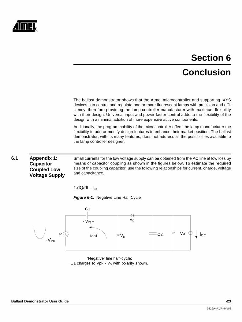
6.1 Appendix 1: Capacitor Coupled Low Voltage Supply
Small currents for the low voltage supply can be obtained from the AC line at low loss bymeans of capacitor coupling as shown in the figures below. To estimate the requiredsize of the coupling capacitor, use the following relationships for current, charge, voltageand capacitance.
1.dQ/dt = IDC
Figure 6-1. Negative Line Half Cycle
AC
C1
VD
VD
C2
“Negative” line half -cycle:C1 charges to Vpk - VD with polarity shown.
VoIch1 IDC
-VPK
- VC1 +
Ballast Demonstrator User Guide -23
7629A–AVR–04/06
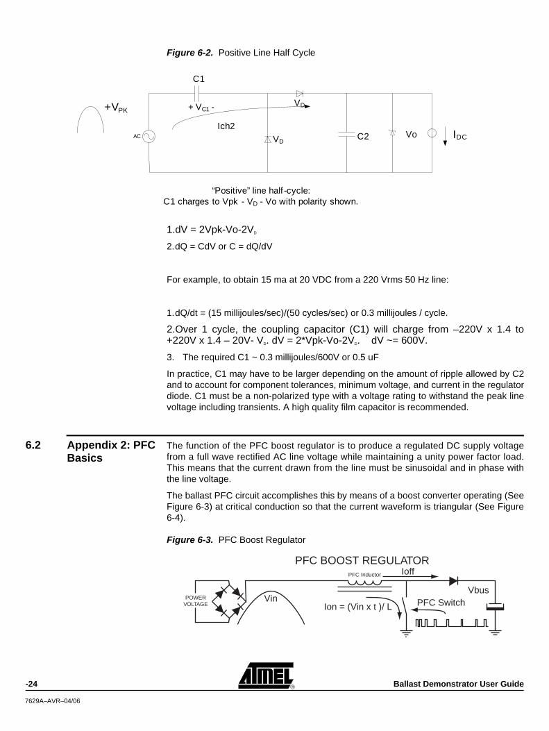
Figure 6-2. Positive Line Half Cycle
1.dV = 2Vpk-Vo-2VD
2.dQ = CdV or C = dQ/dV
For example, to obtain 15 ma at 20 VDC from a 220 Vrms 50 Hz line:
1.dQ/dt = (15 millijoules/sec)/(50 cycles/sec) or 0.3 millijoules / cycle.
2.Over 1 cycle, the coupling capacitor (C1) will charge from –220V x 1.4 to+220V x 1.4 – 20V- VD. dV = 2*Vpk-Vo-2VD. dV ~= 600V.3. The required C1 ~ 0.3 millijoules/600V or 0.5 uF
In practice, C1 may have to be larger depending on the amount of ripple allowed by C2and to account for component tolerances, minimum voltage, and current in the regulatordiode. C1 must be a non-polarized type with a voltage rating to withstand the peak linevoltage including transients. A high quality film capacitor is recommended.
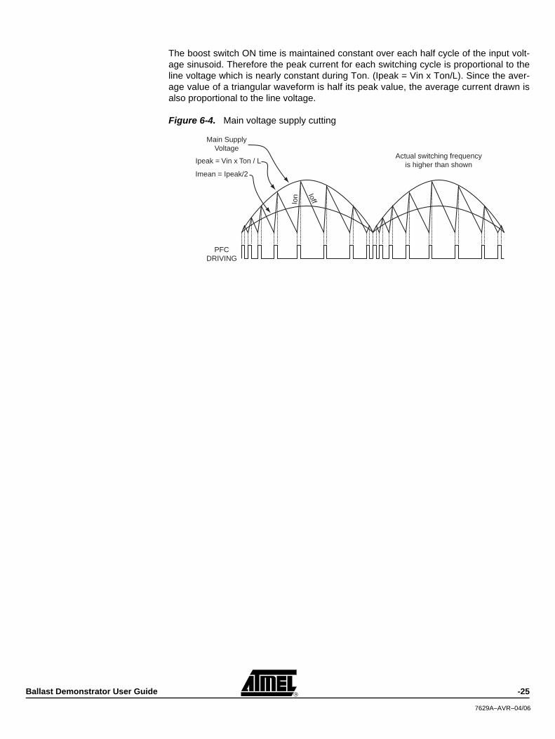
6.2 Appendix 2: PFC Basics
The function of the PFC boost regulator is to produce a regulated DC supply voltagefrom a full wave rectified AC line voltage while maintaining a unity power factor load.This means that the current drawn from the line must be sinusoidal and in phase withthe line voltage.
The ballast PFC circuit accomplishes this by means of a boost converter operating (SeeFigure 6-3) at critical conduction so that the current waveform is triangular (See Figure6-4).
Figure 6-3. PFC Boost Regulator
AC
C1
VD
VD
C2
“Positive” line half -cycle:C1 charges to Vpk - VD - Vo with polarity shown.
VoIch2
IDC
+VPK + VC1 -
PFC Inductor
PFC BOOST REGULATOR
POWERVOLTAGE
VinVbus
Ion = (Vin x t )/ L
Ioff
PFC Switch
-24 Ballast Demonstrator User Guide
7629A–AVR–04/06
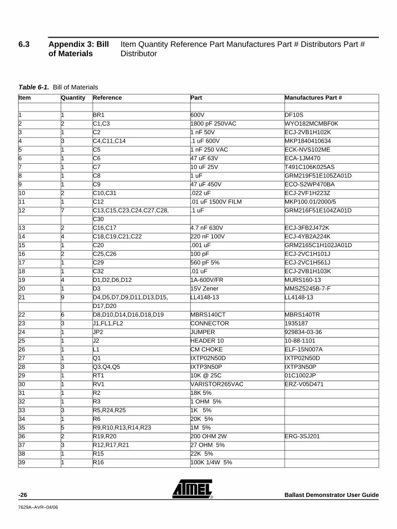
The boost switch ON time is maintained constant over each half cycle of the input volt-age sinusoid. Therefore the peak current for each switching cycle is proportional to theline voltage which is nearly constant during Ton. (Ipeak = Vin x Ton/L). Since the aver-age value of a triangular waveform is half its peak value, the average current drawn isalso proportional to the line voltage.
Figure 6-4. Main voltage supply cutting
PFCDRIVING
Main SupplyVoltage
Ipeak = Vin x Ton / L
Imean = Ipeak/2
Ion Ioff
Actual switching frequencyis higher than shown
Ballast Demonstrator User Guide -25
7629A–AVR–04/06
6.3 Appendix 3: Bill of Materials
Item Quantity Reference Part Manufactures Part # Distributors Part # Distributor
Table 6-1. Bill of MaterialsItem Quantity Reference Part Manufactures Part #
1 1 BR1 600V DF10S2 2 C1,C3 1800 pF 250VAC WYO182MCMBF0K3 1 C2 1 nF 50V ECJ-2VB1H102K4 3 C4,C11,C14 .1 uF 600V MKP18404106345 1 C5 1 nF 250 VAC ECK-NVS102ME6 1 C6 47 uF 63V ECA-1JM4707 1 C7 10 uF 25V T491C106K025AS8 1 C8 1 uF GRM219F51E105ZA01D9 1 C9 47 uF 450V ECO-S2WP470BA10 2 C10,C31 .022 uF ECJ-2VF1H223Z11 1 C12 .01 uF 1500V FILM MKP100.01/2000/512 7 C13,C15,C23,C24,C27,C28, .1 uF GRM216F51E104ZA01D
C3013 2 C16,C17 4.7 nF 630V ECJ-3FB2J472K14 4 C18,C19,C21,C22 220 nF 100V ECJ-4YB2A224K15 1 C20 .001 uF GRM2165C1H102JA01D16 2 C25,C26 100 pF ECJ-2VC1H101J17 1 C29 560 pF 5% ECJ-2VC1H561J18 1 C32 .01 uF ECJ-2VB1H103K19 4 D1,D2,D6,D12 1A-600V/FR MURS160-1320 1 D3 15V Zener MMSZ5245B-7-F21 9 D4,D5,D7,D9,D11,D13,D15, LL4148-13 LL4148-13
D17,D2022 6 D8,D10,D14,D16,D18,D19 MBRS140CT MBRS140TR23 3 J1,FL1,FL2 CONNECTOR 193518724 1 JP2 JUMPER 929834-03-3625 1 J2 HEADER 10 10-88-110126 1 L1 CM CHOKE ELF-15N007A27 1 Q1 IXTP02N50D IXTP02N50D28 3 Q3,Q4,Q5 IXTP3N50P IXTP3N50P29 1 RT1 10K @ 25C 01C1002JP30 1 RV1 VARISTOR265VAC ERZ-V05D47131 1 R2 18K 5%32 1 R3 1 OHM 5%33 3 R5,R24,R25 1K 5%34 1 R6 20K 5%35 5 R9,R10,R13,R14,R23 1M 5%36 2 R19,R20 200 OHM 2W ERG-3SJ20137 3 R12,R17,R21 27 OHM 5%38 1 R15 22K 5%39 1 R16 100K 1/4W 5%
-26 Ballast Demonstrator User Guide
7629A–AVR–04/06
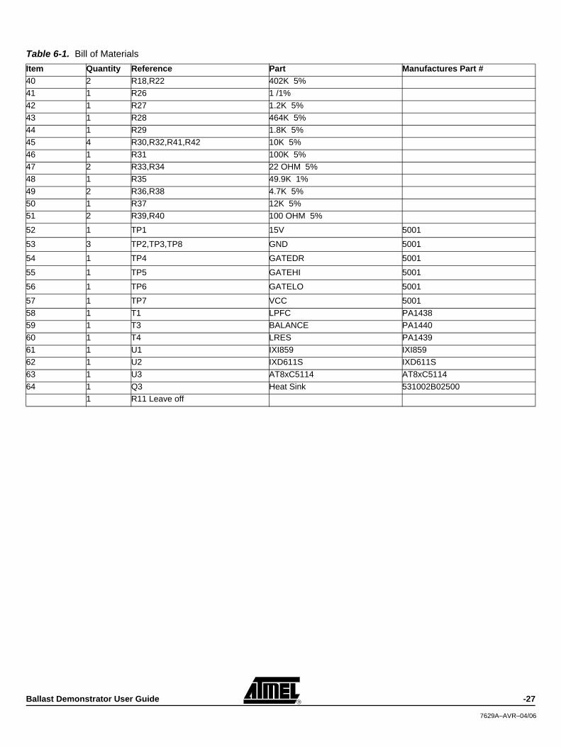
40 2 R18,R22 402K 5%41 1 R26 1 /1%42 1 R27 1.2K 5%43 1 R28 464K 5%44 1 R29 1.8K 5%45 4 R30,R32,R41,R42 10K 5%46 1 R31 100K 5%47 2 R33,R34 22 OHM 5%48 1 R35 49.9K 1%49 2 R36,R38 4.7K 5%50 1 R37 12K 5%51 2 R39,R40 100 OHM 5%
52 1 TP1 15V 5001
53 3 TP2,TP3,TP8 GND 5001
54 1 TP4 GATEDR 5001
55 1 TP5 GATEHI 5001
56 1 TP6 GATELO 5001
57 1 TP7 VCC 500158 1 T1 LPFC PA143859 1 T3 BALANCE PA144060 1 T4 LRES PA143961 1 U1 IXI859 IXI85962 1 U2 IXD611S IXD611S63 1 U3 AT8xC5114 AT8xC511464 1 Q3 Heat Sink 531002B02500
1 R11 Leave off
Table 6-1. Bill of MaterialsItem Quantity Reference Part Manufactures Part #
Ballast Demonstrator User Guide -27
7629A–AVR–04/06
6.4 Appendix 4: Schematic
Figure 6-5.
C7
10
uF
25
V
J1
CO
NN
EC
TOR
1234
C8
1uF
LA
MP
_DC
BO
OS
TV
SUP
FL2 C
ON
NE
CTO
R
L11 L22
L3 3L4 4
FL1
CO
NN
EC
TOR
L11 L22
L3 3L4 4
R9
1M
R1
31
M
SINGLE
LAMP OP
Q3
IXT
P3
N50
P
VCC
R1
2
27
D6
1A-
60
0V/
FR
D1
7
LL4
14
8-1
3
C1
4.1
uF
600
V
R3
0
10K
C9
50u
F 4
75V
R1
5
22K
LA
MP
_DC
RECT. LAMP VOLTAGE DET
.
IGNITION, RAMP, MISSING LAMP DET
.
ANALOG INPUT
R2
91.
8 K
1.25 TO 2.75
NORMA
L
1.00 TO 3.00
END O
F
LIFE T8
t
RT
110
K @
25
C
1 2
R6
20K
TE
MPE
RA
TU
RE
OVERTEMP DET
.
OPEN FILAMENTS DETECTE
D BY 1/2 BRIDGE
CURRENT, ONE LAMP
JUMPER, & RECT LAMP VOLTAGE. OPTION IN CODE TO ACCEPT
ONE LAMP W/D
ALI FL
AG OR FAULT.
0.264 V @ 80
C
1.1V @ 25C
250 uA MAX.
D1
0
MBR
S1
40C
TR
16
100
K 1
/4W
C2
7.1
uF
VCC
R3
3
22
OH
M
HBR
IDG
E_H
I
HA
VER
SIN
E_IN
HA
VER
SIN
E_IN
HA
VER
SIN
E_IN
HA
VER
SIN
E_IN
PFC
_D
RIV
E
HB
RID
GE
_LO
U3
AT8
xC
511
4
P4
.0/A
IN0
1
P4
.1/A
IN1
2
P4
.2AI
N2
3
P4
.3AI
N3
4
P3
.3AI
N4
5
P3
.4AI
N5
6
P3.5
/W1M
07
P3
.2/IN
T0
8
P3.1
/W0M
19
P3.0
/W0M
01
0Vc
c1
1Vs
s1
2R
ST
13
XT
AL1
14
XT
AL2
15
C1
6R
17
Vss
a1
8V
cca
19
Vre
f2
0
D5
LL4
14
8-1
3
R3
5
49.9
K 0
.1%
R3
610
K
D1
8
C2
95
60
pF
1%
D1
9
ZE
RO
CR
OS
SIN
G
LA
MP
_AC
NO
TES
:
R1
41
M
R1
01
M
HIGH FET CURRENT
ALARM
CURRENT SENSE FOR
POWER CALC
LAMP MISSING DET.
LAMP CURRENT DET.
T3 B
AL
AN
CE
16
49
Q1
IXTP
02
N50
D1
2 3
U2
IXD
611
S
HO
7H
IN2
VCC
1
LO
5
LIN
3
CO
M4
VS
6
VB
8
R2
18K
TO-220
C2
1nF
C2
8.1
uF
R3
42
2 O
HM
D3
15
V Z
ene
r
C2
61
00p
F
LAM
P_
CU
RR
ENT
C2
0
.00
1uF
HA
VER
SIN
E_IN
R5
1K
C2
51
00P
F
PFC
_D
RIV
E
BO
OS
TV
SUP
R3
33
0 O
HM
D4
LL4
14
8-1
3
T1
LPF
C
1
36
5
10 8
ZE
RO
CR
OS
SIN
G
VCC
VCC
15V
VCC
VCC
15V
VCC
VCC
VCC
VCC
D1
3
LL4
14
8-1
3
R2
4
1K
HB
RID
GE
_LO
HBR
IDG
E_H
I
D7
LL4
14
8-1
3
C4
.1u
F 6
00V
110/220-VIN
Q4
IXT
P3
N50
P
400V BUS TES
T
RESONANT CAP
LAMP VO
LT DET.
END OF LIFE
DC & A
C
DAC CONTROLLED WINDOW
COMP.
D1
1
LL4
14
8-1
3
R1
1
20
0 O
HM
3 W
Q5
IXT
P3
N50
P
C1
0
.02
uF
CLOSE
PROXIMITY R
21
27
GA
TEH
ID9
LL4
14
8-1
3
C3
0.1
uF
Flourescent Lamp
Flourescent Lamp
C1
18
00
pF
25
0VA
C
VBU
S
TP-8
R3
210
K
C2
4
.1u
F
D8
MBR
S1
40C
T
VCC
C5
1 n
F 6
00 V
D1
5LL
41
48-
13
JP2
JU
MPE
R
12
REMOVE FOR SINGLE LAMP OP.
REMOVE FOR SINGLE LAMP OP.
R1
92
00
OH
M 3
W
Title
Siz
eD
oc
um
ent N
um
be
rR
ev
Da
te:
She
et
of
C-0
50
41
8-1
0C
11
We
dn
esd
ay
, Fe
bru
ary
15
, 200
6
Fire
fly B
alla
stW
L W
illia
mso
n &
AS
SO
C
R2
02
00
OH
M 3
W
C1
65
nF
C1
75
nF
C1
3
.1u
F
C3
21
0nF
R3
810
K
C1
1.1
uF
60
0V
FIL
M
C1
9
220
nF
100
V
VDC
TP1
15V
C1
2.0
1u
F 1
50
0V
FIL
M
R3
910
0
R1
84
00K
-+
BR1 600
V
3
1
4
2
R3
712
K
R2
24
00K
R2
71.
2K
TP2
GN
D
TP8
GN
D
VBU
S
C3
18
00
pF
25
0VA
C
TE
MPE
RA
TU
RE
TE
MPE
RA
TU
RE
TE
MPE
RA
TU
RE
TE
MPE
RA
TU
RE
TE
MPE
RA
TU
RE
TE
MPE
RA
TU
RE
TE
MPE
RA
TU
RE
TE
MPE
RA
TU
RE
TE
MPE
RA
TU
RE
TE
MPE
RA
TU
RE
TE
MPE
RA
TU
RE
TE
MPE
RA
TU
RE
TE
MPE
RA
TU
RE
TE
MPE
RA
TU
RE
TE
MPE
RA
TU
RE
TE
MPE
RA
TU
RE
D2
1A-
60
0V/
FR
TP4
GA
TED
R
VBUS
RV
1
LA
MP
_AC
C1
8
220
nF
100
V
R4
010
0
J2
HE
AD
ER
10
1 2 3 4 5 6 7 8 9 10
D1
2
1A-
60
0V/
FR
T4A
TR
AN
SFO
RM
ER
S1
F1
2
TP5
C2
2
220
nF
100
V
VCC
T4E
TR
AN
SFO
RM
ER
S6
F7
TP6
T4B
TR
AN
SFO
RM
ER
S2
F1
1
C2
1
220
nF
100
V
D1
6
MBR
S1
40C
T
R2
51
K
LAM
P_
CU
RR
ENT
LAM
P_
CU
RR
ENT
LAM
P_
CU
RR
ENT
LAM
P_
CU
RR
ENT
LAM
P_
CU
RR
ENT
LAM
P_
CU
RR
ENT
LAM
P_
CU
RR
ENT
LAM
P_
CU
RR
ENT
D1
4
MBR
S1
40C
T
VCC
R2
61
/1%
T4C
TR
AN
SFO
RM
ER
S3
F1
0
R4
110
K
U1
IXI5
89
VSU
P7
VO
UT
2
VCC
1
GAT
E5
NC
3
IN4
GN
D6
VC
AP
8TP
3
GN
D
L1
CM
CH
OK
E
T4D
TR
AN
SFO
RM
ER
S5
F8
R3
11
00 K
C2
3.1
uF
C6
47
uF
C1
5.1
uF
VOLTAGE DOUBLER
D2
0LL
41
48-
13
C3
1
.02
2uF
BO
OS
TV
SUP
R1
7
27
R2
84
60 K
GA
TEL
OR
23
1M
R4
210
K
D1
1A-
60
0V/
FR
TP7
VCC
0.8 V
-28 Ballast Demonstrator User Guide
7629A–AVR–04/06
Disclaimer: The information in this document is provided in connection with Atmel products. No license, express or implied, by estoppel or otherwise, to anyintellectual property right is granted by this document or in connection with the sale of Atmel products. EXCEPT AS SET FORTH IN ATMEL’S TERMS AND CONDITIONS OFSALE LOCATED ON ATMEL’S WEB SITE, ATMEL ASSUMES NO LIABILITY WHATSOEVER AND DISCLAIMS ANY EXPRESS, IMPLIED OR STATUTORY WARRANTYRELATING TO ITS PRODUCTS INCLUDING, BUT NOT LIMITED TO, THE IMPLIED WARRANTY OF MERCHANTABILITY, FITNESS FOR A PARTICULAR PURPOSE,OR NON-INFRINGEMENT. IN NO EVENT SHALL ATMEL BE LIABLE FOR ANY DIRECT, INDIRECT, CONSEQUENTIAL, PUNITIVE, SPECIAL OR INCIDENTAL DAM-AGES (INCLUDING, WITHOUT LIMITATION, DAMAGES FOR LOSS OF PROFITS, BUSINESS INTERRUPTION, OR LOSS OF INFORMATION) ARISING OUT OF THEUSE OR INABILITY TO USE THIS DOCUMENT, EVEN IF ATMEL HAS BEEN ADVISED OF THE POSSIBILITY OF SUCH DAMAGES. Atmel makes no representations orwarranties with respect to the accuracy or completeness of the contents of this document and reserves the right to make changes to specifications and product descriptions atany time without notice. Atmel does not make any commitment to update the information contained herein. Unless specifically providedotherwise, Atmel products are not suit-able for, and shall not be used in, automotive applications. Atmel’s products are not intended, authorized, or warranted for use as components in applications intended to sup-port or sustain life.
Atmel Corporation Atmel Operations2325 Orchard ParkwaySan Jose, CA 95131, USATel: 1(408) 441-0311Fax: 1(408) 487-2600
Regional HeadquartersEurope
Atmel SarlRoute des Arsenaux 41Case Postale 80CH-1705 FribourgSwitzerlandTel: (41) 26-426-5555Fax: (41) 26-426-5500
AsiaRoom 1219Chinachem Golden Plaza77 Mody Road TsimshatsuiEast KowloonHong KongTel: (852) 2721-9778Fax: (852) 2722-1369
Japan9F, Tonetsu Shinkawa Bldg.1-24-8 ShinkawaChuo-ku, Tokyo 104-0033JapanTel: (81) 3-3523-3551Fax: (81) 3-3523-7581
Memory2325 Orchard ParkwaySan Jose, CA 95131, USATel: 1(408) 441-0311Fax: 1(408) 436-4314
Microcontrollers2325 Orchard ParkwaySan Jose, CA 95131, USATel: 1(408) 441-0311Fax: 1(408) 436-4314
La ChantrerieBP 7060244306 Nantes Cedex 3, FranceTel: (33) 2-40-18-18-18Fax: (33) 2-40-18-19-60
ASIC/ASSP/Smart CardsZone Industrielle13106 Rousset Cedex, FranceTel: (33) 4-42-53-60-00Fax: (33) 4-42-53-60-01
1150 East Cheyenne Mtn. Blvd.Colorado Springs, CO 80906, USATel: 1(719) 576-3300Fax: 1(719) 540-1759
Scottish Enterprise Technology ParkMaxwell BuildingEast Kilbride G75 0QR, Scotland Tel: (44) 1355-803-000Fax: (44) 1355-242-743
RF/AutomotiveTheresienstrasse 2Postfach 353574025 Heilbronn, GermanyTel: (49) 71-31-67-0Fax: (49) 71-31-67-2340
1150 East Cheyenne Mtn. Blvd.Colorado Springs, CO 80906, USATel: 1(719) 576-3300Fax: 1(719) 540-1759
Biometrics/Imaging/Hi-Rel MPU/High Speed Converters/RF Datacom
Avenue de RochepleineBP 12338521 Saint-Egreve Cedex, FranceTel: (33) 4-76-58-30-00Fax: (33) 4-76-58-34-80
Literature Requestswww.atmel.com/literature
© Atmel Corporation 2006. All rights reserved. Atmel®, logo and combinations thereof, and Everywhere You Are® are the trademarks or registeredtrademarks, of Atmel Corporation or its subsidiaries. Other terms and product names may be trademarks of others.
Printed on recycled paper.
7629A–AVR–04/06 /xM