article one cycle control of a pwm rectifier a new approach
TRANSCRIPT

Article
One Cycle Control of A PWM Rectifier a newapproach
Rodrigo Teixeira 1,† , Werbet Da Silva 1,† , Guilherme Pillon 1,† , João Carvalho Neto 2,† ,Elmer Villarreal 3,† , Andrés Salazar 1,†* and Alberto Lock 4,†
1 Department of Computer Engineering and Automation, Federal University of Rio Grande do Norte(DCA-UFRN), Natal 59072-970, Brazil;
[email protected] ; [email protected] ; [email protected] ;[email protected].
2 The Federal Institute of Education, Science and Technology of Rio Grande do Norte (IFRN), Natal, 59015-000,Brazil; [email protected]
3 Department of Natural Sciences, Mathematics, and Statistics, Federal Rural University of Semi-arid(DCME-UFERSA), Mossoró 59625-900, Brazi; [email protected]
4 Centro de Energias Renováveis e Alternativas (CEAR-UFPB), 58051-900, João Pessoa, PB, Brazil;[email protected]
* Correspondence: [email protected]† These authors contributed equally to this work.
Abstract: In this work, it is analyzed a Digital Signal Processor, DSP, based One Cycle Control,OCC, strategy for a Power Factor Corrector, PFC, rectifier, which presents Common-mode Voltage,CMV, immunity. The proposed strategy utilizes an emulated-resistance-controller in closed-loopconfiguration to set up dc-link voltage and achieve unity power factor, UPF. It is shown that if PFCcan achieve UPF condition and if phase voltage is only affected by CMV, then phase current is freefrom CMV, as well as a lead-lag compensator, LLC, to average phase current. Another possiblecondition is also analyzed. The proposal is verified by simulation and experiments.
Keywords: Power factor corrector; One cycle control; Common-mode voltage; Common-modecurrent.
0. INTRODUCTION
One-Cycle Control theory was proposed in [1]. OCC is a nonlinear control theory utilized tocontrol switching converters with only one switching cycle. The controller achieves instantaneousdynamic control of an average value of one of the switching variables from the converter after atransient. The most important feature of OCC is the control of the carrier amplitude, in contrast to thePulse Width Modulation, which controls the variable. One-Cycle control provides low complexity andlow-cost implementation, disturbance rejection, robustness, good stability, and fast dynamic response.OCC has been mostly utilized in the literature to control power factor correction, and it has been appliedin modular multilevel converters [2], a grid-tied single-stage buck-boost DC-AC micro-inverter [3] andVienna Rectifiers [4], a novel multi-converter-based unified power quality conditioner (MCB-UPQC) [5].The study and analysis of harmonics, energy consumption, and power quality of light-emitting diode(LED) lamps equipped in building lighting systems [6]. A novel, two-stage and hybrid approach basedon variational mode decomposition (VMD) and the deep stochastic configuration network (DSCN)for power quality (PQ) disturbances detection and classification in power systems [7]. In powerquality, two of the most significant concerns are harmonic currents and power factor, PF, caused bynonlinear loads. While the former may cause false triggering of protection devices and malfunctioningof motors and transformers, the later reduces available active power at the utility grid. The pastfew decades have witnessed extensive studies on power quality, mainly to satisfy specific standards,i.e., IEEE 519− 1992 [8], that recommend limiting harmonics distortion. To solve these issues for
Preprints (www.preprints.org) | NOT PEER-REVIEWED | Posted: 2 September 2020 doi:10.20944/preprints202009.0036.v1
© 2020 by the author(s). Distributed under a Creative Commons CC BY license.

2
end-consumer, a PWM rectifier is used to substitute each nonlinear load by an active resistance seenfrom the utility grid [9]. In that sense, this rectifier always tries to achieve unity power factor, UPF. Ifthe grid voltage is sinusoidal, then the current drawn by the rectifier must be sinusoidal and in phasewith the voltage, avoiding any current harmonics. Several methods have been proposed to achieveUPF in PWM rectifiers based on the enhanced control-loops concept [10], i.e., an inner current, aninstantaneous power loop, and an outer voltage loop. To force the phase-current to follow voltageloop reference, it is necessary to sense three-phase voltages, a dc-link voltage, and three-phase currents[11] and eventually, use a phase-locked loop, PLL, to guarantee voltage and current synchronization[12]. The control techniques based on this concept use space vector modulation, SVM, Park/Clarketransformations and control coupled terms, like voltage oriented control, VOC, [14], direct powercontrol, DPC, [13], model predictive control (MPC) [15], deadbeat control [16], fuzzy control [17]and neural networks [18]. Nevertheless, these methods are time-consuming, as they rely on systemparameters, requiring complicated online calculation. Resistance-emulation is another techniqueemployed in PWM rectifiers, generally using average value and PWM modulators. In this techniqueis always assumed that UPF is already achieved. There are two main methods based on open-loop,and closed-loop controls [9]. Open-loop controls estimate emulated-resistance, assuming a fixed value[19], while closed-loop methods adjust the emulated-resistance value by feedback [20]. Although thesetechniques were proposed for single-phase boost converters with diode rectifiers, they are complicatedto implement as they employ the four arithmetical operations.
Figure 1. (a) Hardware OCC. (b) Associate waveforms.
Among open-loop methods, One Cycle Control, OCC, originally a hardware technique [21],Figure 1(a), has implemented by a few commercials ICs, or a single chip, constituting a kind ofcost-effective solution. It uses a variable sawtooth-carrier-amplitude, Figure 1(b), and only addingand subtracting operations, contributing to its arithmetic simplicity and performing its control tasksin the only one switching cycle, therein the name OCC, despite this technique was also proposed forthree-phase, six power-switches boost-converter. Besides enhanced control-loops technique, OCC hasnot utilized phase-locked loop (PLL), Park/Clarke transformations, or online parameter calculations,but achieves a high dynamic response and satisfies UPF condition. Moreover, it eliminates the needfor three grid-voltage sensors, which adds control and hardware simplicity. Although this techniquewas applied several times, i.e., inactive power filters (APF) [22], [23], flexible ac transmission systems(FACTs), [28] and photo-voltaic grid-connected inverters (GCI) [24], [32], [27], OCC has presented suchserious instability problems [21], [29], [30], which to solve them, it was necessary to add extra circuitry,sacrificing control and hardware simplicity.
Hence, in order to preserve control and hardware simplicity, OCC was emulated in a DSP system.So a DSP-based software-OCC was proposed in [31], see Figure 1(c) and Figure 1(d). This versionenhances OCC with DSP calculation capability and uses closed-loop resistance emulation. Then, thesoftware offers more possibilities to apply OCC to the most complex control issues than those ofhardware [33], [34], [35]. Besides, unlike enhanced-loops methods mentioned above [11], [12], [14],
Preprints (www.preprints.org) | NOT PEER-REVIEWED | Posted: 2 September 2020 doi:10.20944/preprints202009.0036.v1

3
[13], [15], [16], [17], [18], software-OCC does not need PLL, nor Park/Clarke transformations, noronline parameter calculations, achieving some control simplicity. However, it was not reported anyfurther analysis, in spite DSPs have already applicated to OCC as a control core, i.e., for motor drivers[36], [37], and photovoltaics [32], while OCC runs as a sort of auxiliary circuit. Previous treatmentsto solve stability problems at no-load have sacrificed OCC simplicity once they use an additionalbulky resistor at dc-link [21], [30]. Instead, in [38], [39], [26] to decrease current distortion, an artificialphase-current was created. However, despite the efforts, instability remains when load current fallsbelow a certain limit [43], [28], [42]. On the other side, due to a lack of PLL synchronization, OCC hasexperienced PF derating at high-load [21], [39], [30], [42], [26]. To avoid this, OCC has sacrificed itssimplicity again as they use input voltage multiplexers, and other additional analog and logic circuits[43], [23], [28], [42], [25], requiring the knowledge of 600 angular sectors and to select positive andnegative peak voltages as reference current vectors. In [29], [41] was also necessary to sacrifice OCCsimplicity by adding a few analog multipliers and heavy and bulky inductors (10mH), but sacrificingthe cost-effectiveness of OCC solution. Hence, despite all the efforts, it is apparent that, to date, OCChas been not able, whatsoever, to solve its own problems fully. Above all, even though a few hardwaremethods have solve partially OCC stability issues at no-load [21], [38], [39], [26], [41], and at high-load[43], [29], [42], [25], they were never reported working together over a wide load range. Thus, one ofthe paper’s major contributions is to present a simple and stable OCC system working at no-load andhigh-load.
In this paper, analysis, simulation, and experimental results prove, based on theresistance-emulated controller [31], that software-OCC does not possess instability issues and preservesOCC simplicity and dynamical response, also satisfying UPF condition. The paper is organized asfollows: Section 1 presents a review of software-OCC fundamentals. Section 2 . shows OCC issuesand discusses software-OCC solving method. Section 3 depicts DSP implementation and discussesthe cost-effectiveness of software-OCC. Simulation and experimental results are shown in Section 4.Conclusions are shown in Section 5 .
1. FUNDAMENTALS Of SOFTWARE-OCC
Software-OCC is a PWM, where an average phase-current compares to carrier and controlsystem is integrated into the modulator, similar to hardware-OCC of Figure 1(c) [21]. Nevertheless,unlike hardware-OCC, this version is not a circuit, but a software. Hence, software-OCC implementsOCC features by programming embedded DSP devices and using just a few equations. However, ahigh-performance OCC system is obtained, as using a high-frequency DSP, the one switching-cyclecontrol can be guaranteed. Figure 2(a) displays a three-phase, IGBT PWM rectifier. As inhardware-OCC, it is assumed that,
• The switching frequency fC is much higher than line frequency f , hence the switching period TCis much lower than the line period T, so fC >> f and TC << T.
• The switches in each leg operate in a complementary fashion, i.e., the duty cycle for the upperand bottom switch is dg and dgn = (1− dg), respectively (g = a, b, c), 0 < dg < 1.
• Input impedance seen from the grid is a resistance, similar to the resistance emulation concept in[9]. Besides, software-OCC, Figure 1(c), present the following differences from hardware-OCC,
• i)Multipliers and dividers presence, as they are not much DSP time-consuming [44].• ii) The average method, i.e., a Lead-Lag compensator, LLC, Figure 1(c), decreases delay response
caused by the lagging part, using a leading constant.• iii) Carrier generation uses a triangular waveshape, Figure 1(d), instead of a sawtooth carrier in
the hardware OCC.• iv) Fixed amplitude carrier because of a software DSP limitation.• v) Closed-loop emulated resistance-control, guaranteeing UPF by feedback.• vi) Use of limiters at resistance control output.
Preprints (www.preprints.org) | NOT PEER-REVIEWED | Posted: 2 September 2020 doi:10.20944/preprints202009.0036.v1

4
Except for iv), these differences are a result of superior software-DSP-calculation capability overhardware technique. Applying Kirchhoff voltage law to the r− L branch of Figure 2,
vsa vsb vsc
rA
BC
O RL
C1
C2
ia
I0qa
qan
qb
qbn
qc
qcn
N
V0
L
Figure 2. (a) Three phase, PWM rectifier.
Figure 3. (b) Pole voltage, vGM.
vSa − ria − Ldia
dt= vAN + vNO
vSb − rib − Ldibdt
= vBN + vNO (1)
vSc − ric − Ldicdt
= vCN + vNO
where r is inductor resistance, L is inductor inductance; vSg and ig are grid voltage and phasecurrent, respectively; vGN is pole voltage (G = A, B, C), O is the middle point of dc-link capacitors C1
and C2, vNO is the voltage between neutral of the utility grid and middle point N of dc-link voltage,and V0 and I0 are dc-link voltage and current respectively.
1.1. Analysis of voltage vNO
Examining the former equation, it is apparent that to obtain an exact expression for phase-current,it is necessary to find an analytical expression for voltage vNO. However, although some previousworks indicate that this voltage does not depend on grid frequency [14], [40], the mathematical proofis missing. It is always possible to bypass the problem by assuming some control strategy, as it allowsadditional simplifications, [45], [46]. Hence, considering a balanced system,
vSa + vSb + vSc = 0
ia + ib + ic = 0 (2)
Preprints (www.preprints.org) | NOT PEER-REVIEWED | Posted: 2 September 2020 doi:10.20944/preprints202009.0036.v1

5
Grid voltages are given by,
vSa = Vpcosωt
vSb = Vpcos(ωt− 2π
3) (3)
vSc = Vpcos(ωt +2π
3)
where Vp is voltage amplitude, Vp > 0. Although OCC does not use references [21],[43], formathematical purposes, it could be useful to admit grid voltage, (3), as a virtual phase-currentreference, as phase-current has the same waveshape and in phase with of the grid voltages. In addition,considering a balanced system, (2), and manipulating (1) gives:
VNO =−13
(VAN + VBN + VCN) (4)
The former equation says that voltage VNO is related to pole voltage. Thus, to find an analyticalexpression for VNO could be long and tedious as in a PWM modulator, pole voltage depends on Besselfunctions and Fourier series [47]. The average of VNO is: from the last equation,
1TC
∫ TC
0VNOdt =
−13TC
(∫ TC
0VANdt +
∫ TC
0vBNdt +
∫ TC
0vCNdt) (5)
To find average pole voltage, Figure 2(a), it should be noted that,
1TC
∫ TC
0VGNdt =
1TC
∫ TC
0VGMdt− V0
2(6)
Since average value of pole voltage vGM over switching period is given by (see Figure3(b)),
1TC
∫ TC
0VGMdt =
1TC
[∫ tgn
0V0dt +
∫ TC
tgn0dt] = V0dgn (7)
where tgn = dgnTC. Hence, combining (6) and (7),
1TC
∫ TC
0VGNdt =
V0
2(1− 2dgn) (8)
Moreover, as duty cycle in a PWM modulator is proportional to its reference (3), provided thatfC >> f [47]:
dgn = Dpcos(ωt + φ) (9)
where 0 < Dp < 1, φ is such that, φ = 0 for g = a, φ = −2π3 for g = b, φ = 2π
3 for g = c. Then,combining (5), (8) and (9) yields,
1TC
∫ TC
0VNOdt =
−V0
2(10)
Preprints (www.preprints.org) | NOT PEER-REVIEWED | Posted: 2 September 2020 doi:10.20944/preprints202009.0036.v1

6
A common assumption in hardware OCC is that the current ripple is small and that inductorcurrent works in current continuous mode, CCM [21], so phase-current is proportional to its averagevalue. Thereby, using this assumption in software-OCC, phase-current can be written as,
ig =KTC
∫ TC
0ig(γ)dγ (11)
where K is proportionality constant. Then, for any time t > 0,
tdig(t) = K∫ t
0ig(γ)dγ (12)
Differentiating former equation,
tdig
dt= (K− 1)ig (13)
Combining (1) and (13),
VSg − rig =Lt(K− 1)ig = VGN −VNO (14)
As input impedance seen from the utility grid is assumed a resistance (condition c),
VSg = R0inig (15)
where R0in is assumed input resistance seen from the grid. This resistance is based on loss-free resistor
concept [48], since it transfers all energy from the input to the output port and does not dissipate activepower. Denoting r′ = (K− 1) L
t , where K is a constant (K > 1), and combining (14) and (15),
Rinig = VGN −VNO (16)
Rinig = R0in − (r + r′) (17)
Likewise, resistance Rin is input resistance seen from the grid. Nonetheless, this is the final resistancewhich is controlled by software-OCC, (21) [31], [34]. Averaging (16), it leads to,
Rin1
TC
∫ TC
0igdt =
1TC
∫ TC
0VGNdt− 1
TC
∫ TC
0VNOdt (18)
Combining equations (8), (10) and (18),
Rinigs = −V0(1− dgn) (19)
where igs is average phase-current. The right term of the former equation is the variable amplitude ofthe hardware-OCC carrier. Minus (−) signal means that carrier comes from −V0, when duty cycledgn = 0, to 0 when dgn = 1.
Preprints (www.preprints.org) | NOT PEER-REVIEWED | Posted: 2 September 2020 doi:10.20944/preprints202009.0036.v1

7
Figure 4. Software-OCC waveforms for illustration purposes. fC = 15kHz, f=60Hz. To emphasizethem, it was considered V0 = 450 + 67.5sin(2π f2t)V, f2 = 3.6kHz, Rin = 1Ω. (a) Classical modulator,(23). (b) Modified modulator, (24).
The former equation is coherent to emulated resistance concept, as that resistance was assumedsince operation beginning [9]. Furthermore, this constitutes a classical OCC equation as it achieves thesame level of OCC simplicity, i.e., it uses a sawtooth carrier and does not employ coupled terms, norPark/Clarke transformations [21] [43]. In addition, emulated resistance Rin satisfies,
VSg = Rinig (20)
To ensure that resistance is seen from the grid, satisfying condition c, Rin can become a V0 voltagecontroller. Because if Rin is a V0 controller, it also controls active power P as it depends on V0, sinceP = V0 I0, where I0 is dc link current, Figure 2. Resistance Rin also controls power factor indirectly, sinceactive power P, reactive power Q and apparent power S are related by the expression S =
√P2 + Q2.
In this sense, as S is fixed, if power P is set to a relatively high value (close to S), reactive power Qshould be close to zero. So,
Rin = Kp(V∗0 −V0) + KI
∫(V∗0 −V0)dt (21)
where V∗0 is dc link voltage reference, Kp, KI is proportional and integrative PI constants,respectively. PI constants are positive Kp > 0, KI > 0, to guarantee that Rin > 0, when V∗0 > V0. Rincontroller, named here emulated resistance control, leads to a resistive impedance seen from the grid.Moreover, in frequency domain, Rin controller can be expressed as a function of dc-link voltage error(V∗0 −V0) as,
Rin = (V∗0 −V0)(Kp1 +KI1
s) (22)
According to equation (19), the average current multiplied by Rin is compared to variableamplitude carrier, V0 Atri(t), where carrier Atri(t) = −(1 − dg). This could be the essence of theOCC method when implemented by hardware since a variable carrier amplitude is characteristicalof hardware-OCC [21], [38]. However, as the goal of the system is a software implementation, DSPcharacteristics must be included. In this order, it would be useful to modify classical software-OCCmodulator, (19), as,
qgn =
1, when igs.Rin ≥ V0.Atri(t)0, otherwise
(23)
Preprints (www.preprints.org) | NOT PEER-REVIEWED | Posted: 2 September 2020 doi:10.20944/preprints202009.0036.v1

8
where qgn is the logical state at the gate of lower switch of power converter shown in Figure 1(a). Yet,as dc-link voltage is positive, V0 > 0, former relation can be modified as,
qgn =
1, when (igsRin)
V0≥ Atri(t)
0, otherwise(24)
Former and latter relations are equivalent, as they generate the same firing pulses. The laterrepresents OCC variable-amplitude carrier, Figure 4(a), while the former is adequate for DSPmanipulation, Figure 4(b), as will see later in section IV. Besides, it resembles a PWM modulatorwith zero-sequence injection producing Space Vector PWM, SVPWM [49], or phase-clamping [50], butwithout phase-current distortion.
V0
V0
Limiter
ControllerPI
Figure 5. Rin controller and its maximum Rin−max and minimum Rin−min limits.
2. OCC STABILITY ANALYSIS
There is no simple method to analyze hardware-OCC stability by conventional control theory,as this technique is all except conventional, once control and hardware are integrated, while insoftware-OCC control and hardware are implemented and integrated by software. There are twomain stability issues reported in hardware-OCC i.e., at no-load [21], [38], [30], and high-load [29].However, control theory was not used to study them, but hardware analysis. This might be becauseOCC instability is provoked by over modulation [21] and hardware limitations [29] and not by poles orzeroes misplacement. Stability issues in hardware-OCC can be solved by using an emulated-resistancecontroller Rin of software-OCC [31], and it is max. and min. limiters, Figure 5. The next sub-sectionpresents a model based on emulated-resistance control, which explains hardware-OCC instability andsoftware-OCC solutions to the problem.
2.1. Hardware-OCC Theoretical Background.
In hardware-OCC, voltage Vm is a PI controller of dc voltage, given by [21],
Vm = (V∗0 −V0)(Kp1 +KI1
s) (25)
where Vm is carrier amplitude controller, Fig.5(a), in frequency domain, s = jω, Vm is defined by[21],
Vm =K1RsV0
Rin1(26)
where K1 is a parameter,VSgV0
< K1 < 1 +VSgV0
, RS is current sensor resistance (RS = 1Ω) and Rin1is emulated resistance, Rin1 > 0 , [21]. In addition, as in hardware-OCC firing pulses can be defined as[21], [43],
qgnh =
1, when igs ≥ Vm.Atrih(t)0, otherwise
(27)
Preprints (www.preprints.org) | NOT PEER-REVIEWED | Posted: 2 September 2020 doi:10.20944/preprints202009.0036.v1

9
where qgnh is the logical state at the gate of lower switch of power converter, Figure 1(a), Atrih isfixed carrier amplitude. The former equation represents hardware-OCC modulator since modulatingwave is compared to a variable-amplitude carrier, controlled by Vm > 0, (25). Note that this carrierleads to a multiplication operation, despite OCC arithmetic simplicity. Besides, as for a PWM rectifier,Figure 2, average dc voltage V0 has a voltage ripple V0r related to its peak value V0p [51], see Figure 5,then V0 = V0p + V0r . Hence,
V0 = V0p +I0
8CTSW (28)
where V0r =−I08C , I0 is dc-link current, RL is dc-link load, I0 = V0
RL, C is dc-link equivalent capacitor,
C = C1C2(C1+C2)
, TSW is switching time period, TSW = 2T0, T0 is time period between peaks of voltageripple. Although dc-link capacitor C is assumed so large that voltage ripple is neglected and henceaverage and peak dc-link values are the same, V0 ≈ V0p, [51]. Yet, for practical values of capacitance,only (28) is valid.
2.2. Hardware-OCC Issues
When this technique appeared at first offering a cost-effective and straightforward solution [21],[30], it arises two questions about what kind of simplicity and a solution to what. Answer to the laterwas hardware, control, and arithmetic simplicity [30]. Hardware and control simplicity was almostachieved, section I, but a lack of PLL synchronization could cause PF derating
t
V0r
V0p
V0
Figure 6. DC-link voltage in a PWM rectifier
due to a lack of grid synchronization mechanism, whatever a PLL or any other, and OCC had noone. Besides, arithmetic simplicity, i.e., arithmetic without multiplication and division, is most difficultto achieve. However, to avoid the later, the emblematic OCC variable-carrier was created, (27), but atthe cost of instability at no-load [21]. As a result, through instability and PF derating, the offered OCCsolution simplicity became no more than a nice try. Including the solution cost-effectiveness of theOCC. Above all, although the answer to the former question was power converters [43], [29], [1], [23],[28], [32], [27], it is still open, as it generates another question, (what if the OCC simplicity were true,what additional problems could solve).
1) Stability at no-load: In general, in a PWM rectifier, output power P0 equals input power PTminus power losses, PL, P0 = PT − PL. Then, admitting a proportionality between power losses andinput power,
P0 = K3PT (29)
where K3 is proportional constant. In addition, assuming UPF, input power is given by,
Preprints (www.preprints.org) | NOT PEER-REVIEWED | Posted: 2 September 2020 doi:10.20944/preprints202009.0036.v1

10
PT = 3VSg Ig (30)
where VSg and Ig denotes grid voltage and phase current in frequency domain, respectively, whileoutput power is,
P0 = V0 I0 (31)
Then, combining (29), (30) and (31), it yields,
Ig = K4 I0 (32)
where K4 = V0(3K3VSg)
, I0 is dc current. The former equation says that phase-current Ig is
proportional to I0. Yet, (32) has practical limits given by the sensitivity of the technique. As a smallphase-current could exist when I0 is null, or lower than a threshold value, I0th, causing phase-currentdistortion when Ig is greater than amplitude Vm, as reported in [21], [43], [38], [28], [39], [30], [42], [26].This is since Vm becomes tiny at no-load when V0 tends to its reference V∗0 , (25), which occurs whenV∗0 = V0p and I0 = 0, (28). To explain this phenomenon from an emulated-resistance approach, (26)can be rewritten as,
Rin1 =K1V0
Vm(33)
Which leads to a virtual input resistance Rin1, as a sort of V0 controller. Besides, as in OCC,phase-current varies according to [? ],
Rin1 =VSg
Re + sL(34)
where Re denotes OCC input resistance in frequency domain. Hence, by making Re = Rin1 andcombining (25), (33) and (34),
ma =Ig
Vm=
VSg
K1V0 + L(V∗0 −V0)(sKP1 + KI1)(35)
The equation (35) denotes modulation index ma, as Ig is modulating and Vm is carrier amplitude [21].Applying final value theorem to (35), for a unit step response ( 1
s ) when t→ +∞,
ma = limS→01S
SIg
Vm
VSg
K1V0 + LKI(V∗0 −V0)(36)
When V∗0 = V0p and I0 = 0, V∗0 = V0, (28), so equation (36) yields,
ma =VSg
K1V0(37)
Preprints (www.preprints.org) | NOT PEER-REVIEWED | Posted: 2 September 2020 doi:10.20944/preprints202009.0036.v1

11
Overmodulation ocurrs when ma > 1, (37), as VpV0
> K1 > 0, once VSg = Vpcosωt, (3), ma > 0,
i.e. K1 = 0.25 VpV0
, ma = 4, Vp > 0, V0 > 0. Above all, (37) can explain why previous works did notsuppress fully overmodulation by growing or falling Ig [43], [38], [28], [39], [42], [26], once K1 cannot becontrolled.[21]. Figure 7 illustrates this by ploting ma vs. K1, (37), for 0.67 > K1 > 0.19, Vp = 155.56V,V0 = 467V, when Ig grows 20%(A) and when Ig falls 20% (C). Notice that when K1 ≤ 0.25, the methoddoes not work, as ma > 1.
2) Hardware-OCC PF derating at high-load: As was mentioned earlier, PF derating occurs[29], through a lack of grid synchronization. However, this cannot be predicted by an open-loopresistance-emulator value, i.e., re [12], [21] as in frequency domain it leads to Re =
res , which combined
to (34), it gives Ig = sVSg
(re+s2L) , leading to an admittance angle φv = arctan( IgVSg
) = π2 , which is not true.
However, a better prediction can be obtained by combining (25) and (35),
Ig
VSg=
(V∗0 −V0)(sKP1 + KI1)
[sKP1L(V∗0 −V0) + KI1L(V∗0 −V0) + K1V0]s(38)
Then, combining former equation and (28), φv is given by,
φv = φ1 − arctan[ωLKP1(8C(V∗0 −V0p) + I0TSW)
LKI1(8C(V∗0 −V0p) + I0TSW) + K1(8CV0p + I0TSW)] (39)
∂φ
∂I0=
8ωLCTSWKP1K1V∗0(LKI1 I0TSW + K1(8CV0p − I0TSW))2 + (ωLKP1 I0TSW)2 (40)
where V0p = V∗0 was assumed for simplicity. It can be noticed that the former equation predictsPF derating because admittance angle φv is a decreasing function, confirming previous works [39], [30],[42], [26]. Figure 8 plots equation (39), for Vp = 155.56V, V0p = V∗0 = 467V, K1 = 1. Kp1 = 1, KI1 = 1.This figure confirms that φv is decreasing when I0 increases, i.e. from I0 = 10A (P) to I0 = 20A (N) andI0 = 30A (M).
2.3. Software-OCC Solutions
Although subtle, the main difference between hardware-OCC and software-OCC is voltagecontroller location, which in the later is named Vm and controls carrier, (25), (27), while in the former isnamed Rin and controls modulating, (22), (24). However, only Rin allows OCC to solve instability andPF derating issues. It is not just a matter of implementation, 1) Stability at no-load: As was mentionedearlier, phase-current is proportional to dc current, (32), but only under practical limits, through thesensitivity of OCC modulator. Since a small distorted phase-current could appear when dc currentis less than the threshold current, I0th. In order to avoid this in software-OCC, maximum controllerlimiter Rin−max could be calibrated to set up minimum phase-current Igmin, since Ig =
VSgRin
, (20). Then,as voltage VSg is fixed, minimum phase-current Igmin occurs when the resistance Rinmax is reached, asIgRin = VSg is a hyperbolic curve working at first quadrant, Ig > 0, Rin > 0. That is,
Igmin =VSg
Rinmax(41)
Thereby, to avoid phase-current distortion at no-load, Rinmax must be set up to achieve a minimumphase-current Igmin when dc current is less than I0th . Thus,
Preprints (www.preprints.org) | NOT PEER-REVIEWED | Posted: 2 September 2020 doi:10.20944/preprints202009.0036.v1

12
Ig =
Igmin, when I0 < I0thK4 I0, when I0 ≥ I0th
(42)
Figure 7. Hardware-OCC. (a) ma vs. K1, (37), A: Ig grows 20% B: Without correction. C: Ig falls 20%
Figure 8. Hardware-OCC. (b) Angle φv (10/div) vs. angular frequency (rad/s) as a function of dccurrent I0, V∗0 = V0p = 467V, Tsw = 8.33ms, C = 1000µF, L=1mH, Kp1 = KI1 = KI = 1.
Figure 9 shows a plot of Ig vs. I0, (32), when Igmin = 1.4A, I0th = 0.5A, VSg = 110V, Rinmax =
78.01Ω. Unlike hardware-OCC, a tiny dc-controller value does not provoke overmodulation, so thecurrent distortion becomes simpler to avoid.
2) Software-OCC PF derating at high-load: As at no-load, there is no current distortion, it wouldbe necessary to check if at no-load PF derating could be generated. In this sense, the no-load andhigh-load case must be analyzed for PF derating. Thus, substituting Re = Rin in (34),
Ig =VSg
Rin + sL(43)
Note in the former equation that if denominator left term is very greater than the right one,Rin >> sL, the equation becomes equivalent to (20). However, to achieve UPF, another expression canbe found by combining equations (22) and (45), and relation Rin >> sL,
Ig =VSg
(V∗0 −V0)(KP + KIs )
(44)
Preprints (www.preprints.org) | NOT PEER-REVIEWED | Posted: 2 September 2020 doi:10.20944/preprints202009.0036.v1

13
Relation Rin >> sL can be forced by setting resistance lower limit Rinmin = 10ωL, Figure 5, sincein practice this relation implies Rin ≥ 10ωL Rin ≥ 10ωL. Besides, from expression (44), admittanceangle φ = arctan( Ig
VSgis given by,
φv =π
2− arctan(
ωKPKI
) (45)
It can be noticed that this angle does not depend on dc current, nor dc voltage. Figure 10 shows aplot of admittance angle φvvs.ω, for software-OCC, (45), when KP = 1, KI = 1. This plot independs ondc current.
Figure 9. Software-OCC. (a) Ig vs. I0, (34), with a minimum value, Igmin = 1, VSg = 110V, V∗0 = 467V.
Figure 10. Software-OCC. (b) Angle φv(0.10/div) vs. angular frequency (rad/s) as a function of dccurrent I0, V∗0 = V0p = 467V, TSW = 8.33ms, C = 1000µF, L=1mH, Kp1 = KI1 = KI = 1.
ControllerV0
V0
LLC
LLC
LLC qc
qcn
qb
qbn
qa
qania
ib
ic
ias
ibs
ics
offset
A/DRs
Rt
is’
PI
Figure 11. (a) Software-OCC. (b) Phase-current conditioner
Preprints (www.preprints.org) | NOT PEER-REVIEWED | Posted: 2 September 2020 doi:10.20944/preprints202009.0036.v1

14
3. DSP IMPLEMENTATION
Software-OCC controller, Figure 11(a), employs embedded DSP devices like PWM modulators,analog to digital, A/D, converters and the arithmetic-logic unit, ALU, blocks to perform all itstasks digitally, i.e., arithmetic and logic operations (including multiplication and division), digitalcomparators, digital inverters, PI controllers, output limiters and lead-lag compensators, LLCs. Yet,it is necessary a phase-current conditioner, Figure 11(b), consisting of a Hall-effect current-sensor[52], some operational amplifiers, OP-AMPs, and a few resistors [53] to change phase-current over dcvoltage and then transforms it into digital, through A/D converter, see Appendix A. Hence, it is useda Hall-effect resistor RS (100Ω) to convert current into voltage and a resistor Rt (1KΩ) to attenuate it.Then, a bunch of resistors and OP-AMPs (Att) amplifies this voltage and adds an offset to it to input itto A/D, as in DSP, A/D converter only works with positive voltages [53]. Hence, a proportionalitybetween analog and digital is guaranteed for DSP to perform OCC control operations, once a scalefactor KS (bits /A) is maintained for all currents. For hardware-OCC, something similar occurs, butnow the scale factor is a resistance RS (V/A), since a current-sensor resistor is generally used inhardware systems. Anyway, for the sake of simplicity, to establish an equivalency between hardwareand software-OCC, it is defined in the later, resistor RS as unity, RS = 1Ω, denoting that phase-currentcorresponds to the digital value adopted in DSP control operations. After the digitalizing process,phase-current pass through software implemented LLC, which averages phase-current according to,
F(s) = G0(1 + sτ1)
(1 + sτ2)(46)
where F(s) = Igs(s)Ig(s)
, Igs(s), Ig(s) in frequency domain corresponds to phase and average currentsig and igs, respectively in time domain; G0 is gain, τ1 , τ2 are lead and lag compensator constants. Themain idea of former equation is to average phase-current ig without unwanted delay on phase angle,manipulating τ1 and τ2 values. A further analysis of LLC on software-OCC is performed in [34]. On theother hand, for DSP, carrier waveshape (a sawtooth or a symmetrical triangle) is a choice of DSP-PWMmodulator. Thus, in software-OCC, a triangle carrier is chosen since, for a sinusoidal modulatingwave, it produces less current harmonics than those in a sawtooth carrier [54]. Another DSP choiceis produced when carrier slope (rising or falling) intercepts current, generating an inherent delayrelated to the inverse of the carrier frequency. This does not jeopardize the time control algorithm, asDSP operations are performed between the interceptions. Yet, in software-OCC, a variation in carrieramplitude also involves a variation in carrier frequency, Table.1 [53]. Then, there is no direct methodto change carrier amplitude without vary carrier frequency also. However, in order to solve this issue,focusing on generating the same firing pulses, the OCC modulator equation (23) is modified as (24),which becomes the most suitable expression for DSP implementation as it considers a fixed carrieramplitude. In fact, the software-OCC controller is based on equations (21), (24), Figure 11(a).
Table 1. CARRIER AMPLITUDE AND FREQUENCY FOR DSP TMS3020F335.
Carrier Amplitude (A) fC (kHz)
3750 205000 157500 10
3.1. COST-EFFECTIVENESS SOFTWARE-OCC DISCUSSION.
Although first work on hardware-OCC rectifier might constitute a cost-effective solution [21],it presented such serious stability problems, that its use was not practical, i.e., for APF [55], orfor photovoltaics applications [32]. Later instability solutions performed by hardware at no-loadwere reported, but there was always current distortion when dc current falls below a certain level
Preprints (www.preprints.org) | NOT PEER-REVIEWED | Posted: 2 September 2020 doi:10.20944/preprints202009.0036.v1

15
[43], [38], [28], [39], [42], [26], except when a bulky resistor was placed at dc-link [21], [30]. And athigh-load where complicated circuits [43], [23], [28], [42], [25], or costly systems were used [29], [41].Thereby, despite these works represent a nice try to solve specific problems, they do not providea definitive solution, even sacrificing hardware simplicity, or cost-effectiveness of OCC [21], [30].Furthermore, any of the abovementioned reported works were capable of operating both at no-loadand at high-load. Thus, to compare the fair cost-effectiveness of existing hardware-OCC works withpresent software-OCC, it would be necessary to compare reported works of the same performance,that is, OCC rectifiers operating at a wide range of load. Otherwise, it is like comparing a calculatorwith a computer. Above all, although the present work was implemented by using a TMS 320F28335evaluation board in a laboratory prototype, a pretty cost-effective solution could be found acquiring aDSP chip and its accessories separately, or by using a simpler DSP, or a microcontroller chip, i.e., a PIC.In any case, the present proposal results in a cost-effective solution on a full range of load, at least, forlack of another option.
4. SIMULATION AND EXPERIMENTAL RESULTS
The performance of software-OCC has been verified by simulation by using MATLAB andPSCAD/EMTDC and by experimental using DSP TMS320F28335, for PWM rectifier shown in Figure12. The simulation was presented in Figures 14, 15 and 16 (PSCAD) and in Figure 8 and Figure10 (MATLAB). Experimentals are in Figures 18-Figure 28. Parameter values are in Table. 2. InFigure 17 and Figure 24, Vgrms =110V and V∗0 = 390V, but in Figure18- Figure 23, due to technicalproblems, Vgrms =21V and V∗0 = 100V. Figure 14 presents a simulation result only with hardware-OCCevidencing its instability, while Figure 17 presents a simulation result on stability at no-load andhigh-load conditions for software-OCC. It can be observed that at no-load, it does not presenthardware–OCC stability issues,
vsa vsb vsc
rA
BC
O RL
C1
C2
ia
I0qa
qan
qb
qbn
qc
qcn
N
V0
L
Figure 12. (a) PWM rectifier used in tests.
vsa vsb vsc
LA
B
C
O RL
C1
C2
ia
I0
N
V0
da
dan
db
dbn
dc
dcn
Figure 13. (b) PWM rectifier before start-up.
Preprints (www.preprints.org) | NOT PEER-REVIEWED | Posted: 2 September 2020 doi:10.20944/preprints202009.0036.v1

16
Figure 14. Hardware-OCC. (a) Overmodulation at no-load. Transitory from no-load to high-load(10ms/div). Upper: DC current I0 (5A/div). Middle: Carrier and average current (2V/div). Down:Grid voltage (50V/div) and phase current x 10 (50A/div).
Figure 15. Overmodulation at no-load (5ms/div). Detailed view. Upper: Carrier and average current(0.05V/div). Down: Grid voltage (2.5V/div) and phase current x 10 (2.5A/div).
Figure 16. No overmodulation (5ms/div). Detailed view. Upper: Carrier and average current(0.05V/div). Down: Grid voltage (2.5V/div) and phase current x 10 (2.5A/div).
Preprints (www.preprints.org) | NOT PEER-REVIEWED | Posted: 2 September 2020 doi:10.20944/preprints202009.0036.v1

17
ControllerV0
V0
LLC
LLC
LLC qc
qcn
qb
qbn
qa
qania
ib
ic
ias
ibs
ics
offset
A/DRs
Rt
is’
PI
Figure 17. Software-OCC. Transitory from no-load to high-load (10 ms/div). Upper: DC current I0
(5A/div). Middle: Carrier and average current (0.1u/div). Down: Grid voltage (50V/div) and phasecurrents x 10 (50A/div).
like overmodulation [21] (current distortion), nor present PF derating. This result verify equation(43) when KP1 >> KI1. Experimental results in Figure 18-Figure 28 are dedicated to confirm formerresult, or enhance it. Figure 17 shows software-OCC behavior at start-up at no-load, verifying thatthere is no current distortion, unlike [21], nor even in smaller amount [38], [39], [26]. This is because toavoid current distortion, software-OCC can define minimum current when load current is null, byusing Rin−max, (45). Figure 18 illustrates dc-link voltage response to a current step, from no-load tohigh-load, showing a relatively fast-software-OCC dynamic-response considering dc-link capacitorssize, thus complementing Figures 14, 15 and Figure 16. Figure 19 shows phase-current and Rincontroller response to a current step from no-load to high-load, presenting a high dynamic response,which is according to Figure 17.
Figure 18. Rin controller (x5Ω/V) (2V/div), dc-link current (1A/div), grid voltage (20V/div). andphase current (5A/div) for PWM rectifier transient from no -load to high -load. Hor. 40 ms/div.
Preprints (www.preprints.org) | NOT PEER-REVIEWED | Posted: 2 September 2020 doi:10.20944/preprints202009.0036.v1

18
RinI
0
i(t)a
Figure 19. Rin controller (x5Ω/V) (2V/div), dc-link current (1A/div), grid voltage (20V/div). andphase current (5A/div) for PWM rectifier transient from no -load to high -load. Hor. 40 ms/div.
Figure 20 is a Figure 19 amplification for current-shape better illustration. It can be noticed inthe former figure, that at no-load, when I0 = 0, phase-current is small, but it does not exhibit currentdistortion, as it could be expected considering power balancing in equation (41), but instead, regardinga minimum phase-current, according to equation (42), see Figure 19, Figure 20 and Figure 22. Also, itcan be observed that there is no power factor derating, as occurs in conventional hardware-OCC [21],see Figure 21, and Figure 23, and to preserve power factor, it is not necessary to use bulky inductors,unlike [29], [41], Table. 2. Thus, also confirming Figure 17.
Figure 20. Harmonic spectrum. Phase a current, at no=load. fC = 24kHz. THD=1.36%.
Preprints (www.preprints.org) | NOT PEER-REVIEWED | Posted: 2 September 2020 doi:10.20944/preprints202009.0036.v1

19
Rin
v (t)sa
i(t)a
Figure 21. (20ms/div). Grid voltage (2V/div) and phase-current (1A/div) at high-load, fC = 24 kHz.Phase a.
Figure 22. Harmonic spectrum. Phase a current, at high-load fC = 24 kHz. THD=2.5%.
From Figure 20 and Figure 22, it can be deduced that the present proposal satisfies IEEEStd519−1992 [8], as current distortion is small. Figure 21 shows the proposed controller start-up when theload is high. It illustrates a high dynamic response of software-OCC at high-load and that in suchconditions, there is no PF derating. This result could substitute Figure 19 and Figure 26 results, oncethese figures do not achieve high-load results. On the other hand, Figure 23 shows PF derating vs.phase current at different load conditions. Figure 23 was built from Figure 19 at no-load and Figure 21at high-load. Figure 23 demonstrates that there is a tiny variation when phase currents change. Figure24-Figure 26. illustrate dc-link voltage response to a current step, from high-load to no-load, showinga relatively fast software-OCC dynamic-response due to dc-link capacitors size, thus complementingFigure 17.
Preprints (www.preprints.org) | NOT PEER-REVIEWED | Posted: 2 September 2020 doi:10.20944/preprints202009.0036.v1

20
Figure 23. Power factor vs. phase current.
Figure 24. DC-link voltage V0 (20V/div) and dc-link current I0 (0.5A/div), for PWM rectifier transientfrom no-load to high-load. Vgrms =21V. Hor. 2 s/div.
Figure 25. PWM rectifier transient from high-load to no-load. DC-link voltage (50V/div) and dc-linkcurrent (x4) (0.5A/div). Vgrms =21V. Hor. 0.4 s/div
Preprints (www.preprints.org) | NOT PEER-REVIEWED | Posted: 2 September 2020 doi:10.20944/preprints202009.0036.v1

21
Rin
i(t)a
I0
Figure 26. Rin controller (x5Ω/V) (2V/div), dc-link current (1A/div), grid voltage(20V/div). andphase current (5A/div) for PWM rectifier transient from high-load to no-load. Hor. 40 ms/div.
Table 2. PARAMETERS ON SIMULATION AND EXPERIMENTALS.
Parameter R (Ω) ω(r/s) L(mH) C1(µF) C2(µF) VSg (V) τ1(ms) τ2(ms) fC(kHz)
Simulation 1 377 1 670 670 110 1 0.15 20Experimental 1 377 1 2200 2200 110 1 0.15 25
Figure 27 illustrates the dynamic response of software PWM-OCC (switching frequency:24 kHz,RL : 100Ω) as well as the charging capacitor of the dc-link voltage. It spends approximately 0.55s,which is consistent with C=1100µF, Table. 2, and RL. Since the time constant τ = RLC and chargingcapacitor should last 3τ approx. Although OCC systems use to have a high dynamic response, fordc-link capacitor charging, this response depends on the capacitor value that, in the present case, wasnot possible to change due to the physical stability of Semikron board and laboratory facilities setup,Figure 28.
i(t)a
i(t)b
i(t)c
i(t)+a
i(t)+b
i(t)c
Figure 27. DC-link voltage V0 (300V/div) and phase currents ia, ib and ic (14 A/div), V∗0 = 390V.Vgrms =110V. Hor: 100ms/div.
Preprints (www.preprints.org) | NOT PEER-REVIEWED | Posted: 2 September 2020 doi:10.20944/preprints202009.0036.v1
22
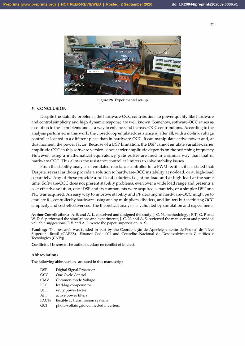
Figure 28. Experimental set-up
5. CONCLUSION
Despite the stability problems, the hardware-OCC contributions to power quality like hardwareand control simplicity and high dynamic response are well known. Somehow, software-OCC raises asa solution to these problems and as a way to enhance and increase OCC contributions. According to theanalysis performed in this work, the closed-loop emulated-resistance is, after all, with a dc-link voltagecontroller located in a different place than in hardware-OCC. It can manipulate active power and, atthis moment, the power factor. Because of a DSP limitation, the DSP cannot emulate variable-carrieramplitude OCC in this software version, since carrier amplitude depends on the switching frequency.However, using a mathematical equivalency, gate pulses are fired in a similar way than that ofhardware-OCC. This allows the resistance controller limiters to solve stability issues.
From the stability analysis of emulated-resistance controller for a PWM rectifier, it has stated that:Despite, several authors provide a solution to hardware-OCC instability at no-load, or at high-loadseparately. Any of these provide a full-load solution, i.e., at no-load and at high-load at the sametime. Software-OCC does not present stability problems, even over a wide load range and presents acost-effective solution, once DSP and its components were acquired separately, or a simpler DSP or aPIC was acquired. An easy way to improve stability and PF derating in hardware-OCC might be toemulate Rin controller by hardware, using analog multipliers, dividers, and limiters but sacrificing OCCsimplicity and cost-effectiveness. The theoretical analysis is validated by simulation and experiments.
Author Contributions: A. S. and A. L. conceived and designed the study; J. C. N., methodology ; R.T., G. P. andW. D. S. performed the simulations and experiments; J. C. N. and A. S. reviewed the manuscript and providedvaluable suggestions; E.V. and A. L. wrote the paper; supervision, A. S.
Funding: This research was funded in part by the Coordenação de Aperfeiçoamento de Pessoal de NívelSuperior—Brasil (CAPES)—Finance Code 001 and Conselho Nacional de Desenvolvimento Científico eTecnológico (CNPq).
Conflicts of Interest: The authors declare no conflict of interest.
Abbreviations
The following abbreviations are used in this manuscript:
DSP Digital Signal ProcessorOCC One Cycle ControlCMV Common-mode VoltageLLC lead-lag compensatorUPF unity power factorAPF active power filtersFACTs flexible ac transmission systemsGCI photo-voltaic grid-connected inverters.
Preprints (www.preprints.org) | NOT PEER-REVIEWED | Posted: 2 September 2020 doi:10.20944/preprints202009.0036.v1

23
References
1. Smedley, K. M.; Cuk, S. One-cycle control of switching converte. In Proceedings of IEEE PESC 91, Cambridge,1991; pp.888–896.
2. Zhao, B.; Huangfu, Y.; Abramovitz, A. Derivation of OCC Modulator for Grid-Tied Single-Stage Buck-BoostInverter Operating in the Discontinuous Conduction Mode. Energies. 2020 , 13(3168), 1–15.
3. Tian, X.; Ma, Y.; Yu, J.; Wang, C.; H. Cheng, H. A Modified One-Cycle-Control Method for Modular MultilevelConverters. Energies. 2019 , 12(157), 1–17.
4. Wang, C.; Liu, J.; Cheng, H. ; Zhuang, Y.; Zhao, Z. A Modified One-Cycle Control for Vienna Rectifiers withFunctionality of Input Power Factor Regulation and Input Current Distortion Mitigation. Energies. 2019 ,12(3375), 1–20.
5. Yang, B. ; Liu, K. ; Zhang, S. ; Zhao, J. Design and Implementation of Novel Multi-Converter-Based UnifiedPower Quality Conditioner for Low-Voltage High-Current Distribution System. Energies. 2018 , 11(3150),1–21.
6. Phannil, N. ; Jettanasen, C.; Ngaopitakkul, A. Harmonics and Reduction of Energy Consumption in LightingSystems by Using LED Lamps. Energies. 2018 , 11(3169), 1–27.
7. Cai, K. ; Alalibo, B. P. ; Cao, W.; Liu, Z. ; Wang, Z. ; Li, G. Hybrid Approach for Detecting andClassifying Power Quality Disturbances Based on the Variational Mode Decomposition and Deep StochasticConfiguration Network. Energies. 2018 , 11(3040), 1–18.
8. IEEE. Recommended Practice and Requirements for Harmonic Control in Electric Power Systems. IEEEStandard 519-1992, 1992.
9. Erickson, R. W. Fundamentals of Power Electronics. Kluwer Academic Publishers. 2000.10. Rodriguez, J. R. ; Dixon, J. W. ; Espinoza, J. R. ; Pontt, J. ; Lezana, P. PWM regenerative rectifiers: state of the
art. IEEE Transactions on Industrial Electronics. 2005, 52(1), 5–22.11. Hartman, M. ; Ertl, H. ; Kolar, J. W. Current control of three phase rectifier system using three independent
current controllers. IEEE Transactions Power Electronics.2013,28(8), 2088–3000.12. Chung, S. K. Phase-locked loop for grid-connected three-phase power conversion systems. IEE Proc-Electr.
Power Appl. 2000, 147(3),213–219.13. Monfared, M.; Rastegar, H. ; Kojabadi, H. M. High performance direct instantaneous power control of PWM
rectifiers. Energy Conversion and Management.2010, 51(5), 947–954.14. Kazmierkowski, M. ; Malesani, L. Current control techniques for three-phase voltage-source PWM converters:
A survey. IEEE Transactions on Industrial Electronics. 1998, 45(5), 691–703.15. Bouafia, A. ; Gaubert, J. ; Krim, F. Design and implementation of predictive current control of three-phase
PWM rectifier using space-vector modulation (SVM). Energy Conversion and Management. 2010, 51(12),2473–2481.
16. Malesani, L. ; Mattavelli, P. ; Buso, S. Robust dead-beat current control for PWM rectifier and active filters.IEEE Transactions on Industry Applications. 1999, 35(3),613–620.
17. Dixon, J. ; Contardo, J. ; Moran, L. A Fuzzy-Controlled Active Front-End Rectifier with Current HarmonicFiltering Characteristics and Minimum Sensing Variables. IEEE Transactions Power Electronics. 1999,14(4),724–729.
18. Coteli, R.; Acikgoz, H. ; Ucar, F. ; Dandil, B. Design and implementation of Type-2 fuzzy neural systemcontroller for PWM rectifiers. International Journal of Hydrogen Energy. 2017,42(32),20759–20771.
19. Chattopadhyay, S. ; Ramanarayanan, V. Digital Implementation of a Line Current Shaping Algorithm forThree Phase High Power Factor Boost Rectifier Without Input Voltage Sensing. IEEE Transactions PowerElectronics. 2004, 19(3),709–711.
20. Maksimovic, D. ; Jang, Y. ; Erickson, R. W. Nonlinear-carrier control for high-power-factor boost rectifiers.IEEE Transactions Power Electronics. 1996, 11(4), 578–584.
21. Qiao, C. ; Smedley, K. M. Unified constant-frequency integration control of three-phase standard bridgeboost rectifiers with power-factor correction. IEEE Transactions on Industrial Electronics. 2003, 50,100–107.
22. Qiao, C. ; Smedley, K. M. Three-Phase Bipolar Mode Active Power Filters. IEEE Transactions on IndustryApplications. 2002 38(1), 149–158.
23. Qiao, C. ; Jin, T. ; Smedley, K. M. One-cycle control of three-phase active power filter with vector operation.IEEE Transactions on Industrial Electronics. 2004 51(2), 455–463.
Preprints (www.preprints.org) | NOT PEER-REVIEWED | Posted: 2 September 2020 doi:10.20944/preprints202009.0036.v1

24
24. Chen, Y. ; Smedley, K. M. A cost-effective single-stage inverter with maximum power point tracking. IEEETransactions Power Electronics. 2004, 45(2), 1289–1294.
25. Jin, T. ; Li, L. ; K. Smedley, K. A universal vector controller for three-phase PFC, APF, STATCOM, andgrid-connected inverter. Proceedings of 19th Ann., Appl. Power Electron, 2004; pp. 594–600.
26. Chatterjee, K. ; Ghodke, D. V. ; Chandra, A. ; Al-Haddad, K. Modified one cycle controlled load compensator.IET Power Electronics. 2011, 4(4),481–490.
27. Chen, Y. ; Smedley, K. M. Three-Phase Boost-Type Grid-Connected Inverter. IEEE Transactions PowerElectronics. 2008, 23(5),2301–2309.
28. Jin, T.; Li, L. ; Smedley, K. M. A Universal Vector Controller for Four-Quadrant Three-Phase Power Converters.IEEE Trans. Circ. and Syst. I. Regular papers. 2007, 54(2),377–390.
29. Ghodke, D. V.; Sreeraj, E. S.; Chatterjee, K.; Fernandes, B. G. One-Cycle-Controlled Bidirectional AC-to-DCConverter with Constant Power Factor. IEEE Transactions on Industrial Electronics. 2009,56(5), 1499–1519.
30. Smedley, K. ; Zhou, L. ; Qiao, C. Unified constant-frequency integration control of active powerfilters-steady-state and dynamics. IEEE Transactions Power Electronics. 2001, 16(3), 428–436.
31. Lock, A. S. ; Da Silva, E. R. C.; Elbuluk, M. E. ; Fernandes, D. A. A hybrid current control for a controlledrectifier. IEEE Energy Conversion Congress and Exposition (ECCE) 2010; pp.920–926.
32. Fortunato, M. ; Giustiniani, A. ; Petrone, G. ; Spagnuolo, G. ; Vitelli, M. Maximum Power Point Tracking in aOne-Cycle-Controlled Single-Stage Photovoltaic Inverter. IEEE Transactions on Industrial Electronics. 2008,55(7), 2684–2693.
33. Lock, A. S. ; Da Silva, E. R. C.; Elbuluk, M. E. ; Fernandes, D. A. Torque control of induction motor drivesbased on One-Cycle Control method. IEEE- IAS Annual Meeting 2012; 1–8.
34. Lock, A. S. ; Da Silva, E. R. C.; Elbuluk, M. E. ; Fernandes, D. A. An -OCC strategy for common-mode currentrejection. IEEE Transactions on Industry Applications. 2016, 52(6), 4935–4945.
35. Bento, A. M. ; Lock, A. S. ; Da Silva, E. R. C. ; Fernandes, D. A., Hybrid one-cycle control technique forthree-phase power factor Control. IET Power Electronics. 2018, 11(3),484–490.
36. Primavera, S. ; Rella, G. Maddaleno, F. Smedley, K. ; Abramovitz, A. One-cycle controlled three-phaseelectronic load. IET Power Electronics. 2012, 5(6),827–832.
37. Niasar, A. H. ; Moghbeli, H. ; Kashani, E. B. A Low-Cost Sensorless BLDC Motor Drive using One-CycleCurrent Control Strategy. IEEE ICEE. 2014, 659–664.
38. Vamanan, N. ; John, V. Dual comparison One Cycle Control for single phase AC to DC converters. IEEETransactions on Industry Applications. 2016 52(4), 3267–3278.
39. Ghodke, D. V. ; Chatterjee, K. ; Fernandes, B. G. Modified One-Cycle Controlled BidirectionalHigh-Power-Factor AC-to-DC Converter. IEEE Transactions on Industrial Electronics. 2008, 55(6),2459–2472.
40. Hava, A. M. ; Un, E. Performance Analysis of Reduced Common-Mode Voltage PWM Methods andComparison with Standard PWM Methods for Three-Phase Voltage-Source Inverters. IEEE TransactionsPower Electronics. 2009, 45(2),782–793.
41. Ghodke, A. A. ; Chatterjee, K. One-cycle-controlled bidirectional three-phase unity power factor ac/dcconverter without having voltage sensors. IET Power Electronics. 2005, 5(9),1944–1955.
42. Chen, Y. ; Smedley, K. M. Parallel operation of one-cycle controlled three-phase PFC rectifiers. IEEETransactions on Industrial Electronics. 2007, 54(6),3217–3224.
43. Chen, G.; Smedley, K. M. Steady-State and Dynamic Study of One-Cycle-Controlled Three-PhasePower-Factor Correction. IEEE Transactions on Industrial Electronics. 2005, 52(2),355–362.
44. Texas Instruments (2012) SPRS439M: TMS320F28335 Data Manual [Online]. Available : http : //www.ti.com.45. Lai, R. ; Wang, F. ; Burgos, R. ; Boroyevich, D. ; Jiang, D. ; Zhang, D. Average Modeling and Control Design
for VIENNA-Type Rectifers Considering the DC-Link Voltage Balance. IEEE Transactions Power Electronics.2009, 24(11), 2509–2521.
46. Lee, D. ; Lim, D. AC Voltage and Current Sensorless Control of Three-Phase PWM Rectifiers. IEEE TransactionsPower Electronics. 2002, 17(6),883–890.
47. Holmes, D. G. ; Lipo, T. A. Pulse Width Modulation for Power Converters, New York: Wiley, 2003.48. Singer, S. ; Smilovitz, D. Transmission line-based loss free resistor, IEEE Trans. Circ. and Syst. I. Fund theory
and app. 1994, 41(2), 120–126.49. Blasko, V. A hybrid PWM strategy combining modified space vector and triangle comparison methods.
Proceedings of Conf. Rec. PESC 1996. 1996; pp.872–1878.
Preprints (www.preprints.org) | NOT PEER-REVIEWED | Posted: 2 September 2020 doi:10.20944/preprints202009.0036.v1

25
50. Hava, A. M. ; Kerkman, R. J. ; Lipo, T. A. Simple analytical and graphical methods for carrier-based PWM-VSIdrives. IEEE Transactions Power Electronics. 1999, 14(1),49–61.
51. Mohan, N. ; Undeland, T. M. ; Robbins, W. P. Power Electronics Converters, Applications, and Design. JohnWiley & sons. Third edition, 2002.
52. LEM, CurrentsensorLA25− NPhttps : //uk.rs− online.com/web/p/current− transducers/0286311/.53. Texas Instruments, Inc., Using PWM output as a digital-to-analog converter on a TMS320F28X, Dallas, TX,
USA, Appl. Rep. SPAA88A.(2008).[Online].Available : http : //www.ti.com.54. Sun, J. Pulse-width modulation in dynamics and control of switched electronic systems. Springer London,
2012.55. Qasim, M. ; Kanjiya, P. ; Khadkikar, V. Artificial-neural-network-based phase-locking scheme for active
power filters. IEEE Transactions on Industrial Electronics. 2014, 61(8),3857–3866.
Sample Availability: Samples of the compounds ...... are available from the authors.
Preprints (www.preprints.org) | NOT PEER-REVIEWED | Posted: 2 September 2020 doi:10.20944/preprints202009.0036.v1