arm cortex-a8 cpu module family ultra line filehardware manual arm cortex-a8 cpu module family dave...
TRANSCRIPT
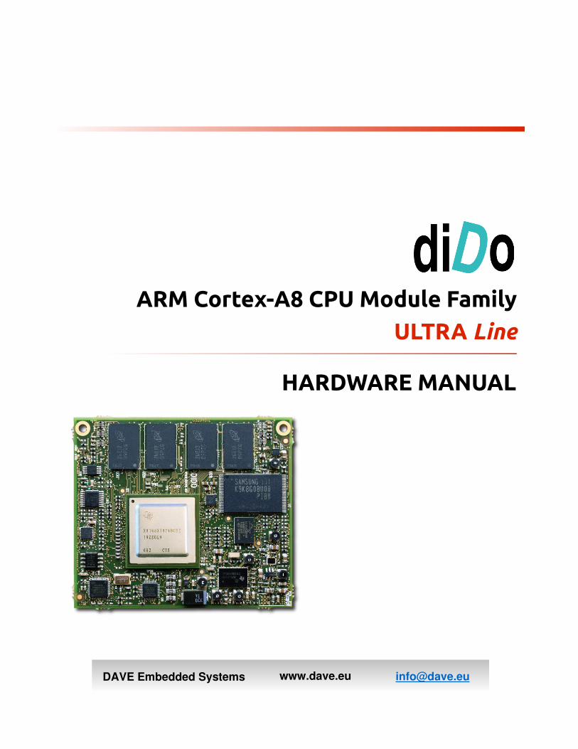
HARDWARE MANUAL
ARM Cortex-A8 CPU Module Family
DAVE Embedded Systems www.dave.eu [email protected]
ULTRA Line
D i d o H a r d w a r e M a n u a l v . 1 . 0 . 5
<Page intentionally left blank>
August, 2014 2/78
D i d o H a r d w a r e M a n u a l v . 1 . 0 . 5
Table of Contents1 Preface.....................................................................................................................................6
1.1 About this manual.............................................................................................................61.2 Copyrights/Trademarks.....................................................................................................61.3 Standards..........................................................................................................................61.4 Disclaimers.......................................................................................................................61.5 Warranty............................................................................................................................61.6 Technical Support.............................................................................................................71.7 Related documents...........................................................................................................81.8 Conventions, Abbreviations, Acronyms............................................................................8
2 Introduction.............................................................................................................................112.1 Product Highlights...........................................................................................................122.2 Block DiagramBlock Diagram.........................................................................................132.3 Feature Summary...........................................................................................................14
3 Design overview.....................................................................................................................163.1 “DaVinci” DM814x / “Sitara” AM387x CPU.....................................................................163.2 DDR3 memory bank.......................................................................................................183.3 NOR flash bank...............................................................................................................183.4 NAND flash bank............................................................................................................183.5 Memory Map...................................................................................................................193.6 Power supply unit...........................................................................................................193.7 CPU module connectors.................................................................................................19
4 Mechanical specifications......................................................................................................214.1 Board Layout...................................................................................................................214.2 Connectors......................................................................................................................23
5 System Logic..........................................................................................................................245.1 Power..............................................................................................................................245.2 PMIC...............................................................................................................................245.3 Reset...............................................................................................................................24
5.3.1 MRST (J2.102)........................................................................................................245.3.2 PORSTn (J2.109)....................................................................................................245.3.3 RSTOUTn (J2.91)....................................................................................................255.3.4 CPU_RESETn (J2.15).............................................................................................255.3.5 JTAG_TRSTn (J2.100)............................................................................................25
5.4 Voltage monitor...............................................................................................................255.5 Boot options....................................................................................................................25
5.5.1 Default boot configuration.......................................................................................265.5.2 Boot sequence customization.................................................................................27
5.6 Clock scheme.................................................................................................................275.7 Recovery.........................................................................................................................27
5.7.1 JTAG Recovery.......................................................................................................275.7.2 UART Recovery.......................................................................................................28
August, 2014 3/78
D i d o H a r d w a r e M a n u a l v . 1 . 0 . 5
5.7.3 SD/MMC Recovery..................................................................................................285.8 Multiplexing.....................................................................................................................285.9 RTC.................................................................................................................................29
6 Pinout table............................................................................................................................306.1 Carrier board mating connector J1.................................................................................326.2 Carrier board mating connector J2.................................................................................386.3 CPU module mount options............................................................................................456.4 Additional notes...............................................................................................................46
6.4.1 EN_BCK_LS............................................................................................................467 Peripheral interfaces..............................................................................................................47
7.1 Digital Video Output (DVO).............................................................................................477.1.1 VOUT0.....................................................................................................................477.1.2 VOUT1.....................................................................................................................48
7.2 HDMI...............................................................................................................................497.3 Analog SDTV out............................................................................................................507.4 Digital Video Input ports..................................................................................................51
7.4.1 VIN0.........................................................................................................................527.4.2 VIN1.........................................................................................................................54
7.5 Ethernet ports.................................................................................................................557.5.1 EMAC_RMREFCLK................................................................................................567.5.2 Ethernet 10/100.......................................................................................................567.5.3 Gigabit EMAC..........................................................................................................57
7.6 CAN ports.......................................................................................................................587.6.1 DCAN0.....................................................................................................................587.6.2 DCAN1.....................................................................................................................58
7.7 UARTs.............................................................................................................................597.7.1 UART0.....................................................................................................................597.7.2 UART3.....................................................................................................................607.7.3 UART5.....................................................................................................................60
7.8 MMC/SD channels..........................................................................................................617.8.1 MMC/SD/SDIO0......................................................................................................617.8.2 MMC/SD/SDIO1......................................................................................................627.8.3 MMC/SD/SDIO2......................................................................................................63
7.9 USB ports........................................................................................................................637.9.1 USB0.......................................................................................................................637.9.2 USB1.......................................................................................................................647.9.3 USB2.......................................................................................................................647.9.4 Other USB signals...................................................................................................64
7.10 Touchscreen..................................................................................................................657.11 EEPROM.......................................................................................................................657.12 Keypad controller..........................................................................................................657.13 PCI Express..................................................................................................................667.14 SPI buses......................................................................................................................67
August, 2014 4/78
D i d o H a r d w a r e M a n u a l v . 1 . 0 . 5
7.14.1 SPI1.......................................................................................................................677.14.2 SPI2.......................................................................................................................687.14.3 SPI3.......................................................................................................................68
7.15 I2C buses......................................................................................................................697.15.1 I2C2.......................................................................................................................697.15.2 I2C3.......................................................................................................................69
7.16 SATA.............................................................................................................................707.17 Audio interfaces............................................................................................................70
7.17.1 McASP2.................................................................................................................717.18 GPIOs...........................................................................................................................717.19 Local Bus......................................................................................................................71
8 Operational characteristics....................................................................................................758.1 Maximum ratings.............................................................................................................758.2 Recommended ratings....................................................................................................758.3 Power consumption........................................................................................................75
8.3.1 Set 1........................................................................................................................768.3.2 Use cases................................................................................................................76
8.4 Heat Dissipation..............................................................................................................779 Application notes....................................................................................................................78
Index of Tables Tab. 1: Related documents........................................................................................................8 Tab. 2: Abbreviations and acronyms used in this manual..........................................................9 Tab. 3: CPU, Memories, Busses..............................................................................................14 Tab. 4: Peripherals...................................................................................................................15 Tab. 5: Electrical, Mechanical and Environmental Specifications............................................15 Tab. 6: DM814x/AM387x comparison......................................................................................18 Tab. 7: DDR2 specifications.....................................................................................................18 Tab. 8: NOR flash specifications..............................................................................................18 Tab. 9: NAND flash specifications............................................................................................19 Tab. 10: ZFF form factor – example of pinout differences.......................................................20
Illustration IndexFig. 1: DIDO CPU module.........................................................................................................11Fig. 2: DIDO (top-right), NAON (top-left) and MAYA (bottom)...................................................11Fig. 3: DIDO SOM (top view)....................................................................................................12Fig. 4: Board layout - top view..................................................................................................21Fig. 5: Board layout - size view.................................................................................................22Fig. 6: Connectors layout..........................................................................................................23Fig. 7: Simplified schematics of EN_BCK2_LS internal pin configuration................................46
August, 2014 5/78

D i d o H a r d w a r e M a n u a l v . 1 . 0 . 5
1 Preface
1.1 About this manualThis Hardware Manual describes the DIDO CPU modules family design and functions.Precise specifications for the Texas Instruments DM814x and AM387x processors can be found in the CPU datasheets and/or reference manuals.
1.2 Copyrights/TrademarksEthernet® is a registered trademark of XEROX Corporation.All other products and trademarks mentioned in this manual are property of their respective owners.All rights reserved. Specifications may change any time withoutnotification.
1.3 StandardsDAVE Embedded Systems Srl is certified to ISO 9001 standards.
1.4 DisclaimersDAVE Embedded Systems does not assume any responsibilityabout availability, supplying and support regarding all the products mentioned in this manual that are not strictly part of the DIDO CPU module.DIDO CPU Modules are not designed for use in life support appliances, devices, or systems where malfunction of these products can reasonably be expected to result in personal injury. DAVE Embedded Systems customers who are using or selling these products for use in such applications do so at theirown risk and agree to fully indemnify DAVE Embedded Systems for any damage resulting from such improper use or sale.
1.5 WarrantyDIDO is warranted against defects in material and
August, 2014 6/78
D i d o H a r d w a r e M a n u a l v . 1 . 0 . 5
workmanship for the warranty period from the date of shipment. During the warranty period, DAVE Embedded Systems will at its discretion decide to repair or replace defective products. Within the warranty period, the repair of products is free of charge as long as warranty conditions are observed.The warranty does not apply to defects resulting from improperor inadequate maintenance or handling by the buyer, unauthorized modification or misuse, operation outside of the product’s environmental specifications or improper installation or maintenance.DAVE Embedded Systems will not be responsible for any defects or damages to other products not supplied by DAVE Embedded Systems that are caused by a faulty DIDO module.
1.6 Technical SupportWe are committed to making our product easy to use and will help customers use our CPU modules in their systems. Technical support is delivered through email to our valued customers. Support requests can be sent to [email protected] upgrades are available for download in the restricted access download area of DAVE Embedded Systems web site: http://www.dave.eu/reserved-area. An account is required to access this area and is provided to customers who purchase thedevelopment kit (please contact [email protected] for account requests)..Please refer to our Web site at http://www.dave.eu/dave-cpu-module-dm814x-dido.html for the latest product documentation, utilities, drivers, Product Change Notifications, Board Support Packages, Application Notes, mechanical drawings and additional tools and software.
August, 2014 7/78
D i d o H a r d w a r e M a n u a l v . 1 . 0 . 5
1.7 Related documents
Document Location
DAVE EmbeddedSystems Developers Wiki
http://wiki.dave.eu/index.php/Main_Page
TMS320DM814x DaVinciTechnical Reference Manual
http://www.ti.com/litv/pdf/sprugz8d
DM814x Overview(on TI Embedded Processors Wiki )
http://processors.wiki.ti.com/index.php/DM814x_Overview
Integration guide (on DAVE Embedded Systems Developers Wiki)
http://wiki.dave.eu/index.php/Integration_guide_%28Dido%29
Tab. 1: Related documents
1.8 Conventions, Abbreviations, Acronyms
Abbreviation Definition
BTN Button
DSP Digital Signal Processor
DVO Digital Video Output
GPI General purpose input
GPIO General purpose input and output
GPO General purpose output
HDVPSS HD Video Processing Subsystems
HDVCIP HD Video Image Coprocessing
NELK NAON Embedded Linux Kit
PCB Printed circuit board
August, 2014 8/78
D i d o H a r d w a r e M a n u a l v . 1 . 0 . 5
Abbreviation Definition
RTC Real time clock
SOM System on module
VIP Video Input Port
PMIC Power Management Integrated Circuit
ZFF Z Form Factor
Tab. 2: Abbreviations and acronyms used in this manual
August, 2014 9/78
D i d o H a r d w a r e M a n u a l v . 1 . 0 . 5
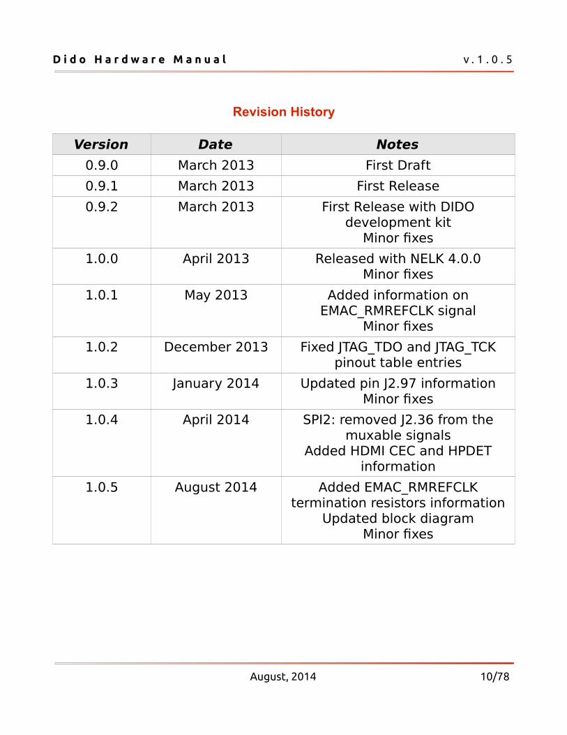
Revision History
Version Date Notes
0.9.0 March 2013 First Draft
0.9.1 March 2013 First Release
0.9.2 March 2013 First Release with DIDOdevelopment kit
Minor fixes
1.0.0 April 2013 Released with NELK 4.0.0Minor fixes
1.0.1 May 2013 Added information onEMAC_RMREFCLK signal
Minor fixes
1.0.2 December 2013 Fixed JTAG_TDO and JTAG_TCKpinout table entries
1.0.3 January 2014 Updated pin J2.97 informationMinor fixes
1.0.4 April 2014 SPI2: removed J2.36 from themuxable signals
Added HDMI CEC and HPDETinformation
1.0.5 August 2014 Added EMAC_RMREFCLKtermination resistors information
Updated block diagramMinor fixes
August, 2014 10/78

D i d o H a r d w a r e M a n u a l v . 1 . 0 . 5
2 IntroductionDIDO is a ready-to-use CPU module/SOM family, based on Texas InstrumentsCortex-A8 high performanceapplication processor from DM814x (“DaVinci”) and AM387x (“Sitara”) models.DIDO is is the cutting edgesolution for a high range ofapplications, including videosurveillance cameras,medical video analysis,smart home controllers,security systems,automation and point ofservice.
DIDO is the first product of DAVE Embedded Systems ULTRA Line CPU modules class, which includes best-in-class solutions and full-featured SOMs.
DIDO shares the same DM814x processor with MAYA (LITE Line) and NAON (ESATTA Line) and is built with the same connectors format (ZFF) as NAON and LIZARD (ESATTA Line).
August, 2014 11/78
Fig. 1: DIDO CPU module
Fig. 2: DIDO (top-right), NAON(top-left) and MAYA (bottom)
D i d o H a r d w a r e M a n u a l v . 1 . 0 . 5
2.1 Product Highlights Top class CPU module family based on Texas
Instruments DM814x/AM387x processors models.
ARM Cortex-A8 architecture @ up to 1 GHz
Up to 2 GB DDR3 @ 533 MHz SDRAM
HD Video Encoding/Decoding Capabilities (High-Definition Video Image Coprocessing – HDVICP v2engine)
Multiple video input and output channels
C674x DSP engine (available on DM8148)
NEON Multimedia co-processor and PowerVR® SGX 530 Vector/3D Graphics Engine
On-board flash (NOR and NAND) storage
Small form factor
Rich interfaces set including PCI Express, dual CAN, dual Ethernet, SATA and native 3.3V I/O
NAON and LIZARD (ESATTA Line) pinout compatible
August, 2014 12/78
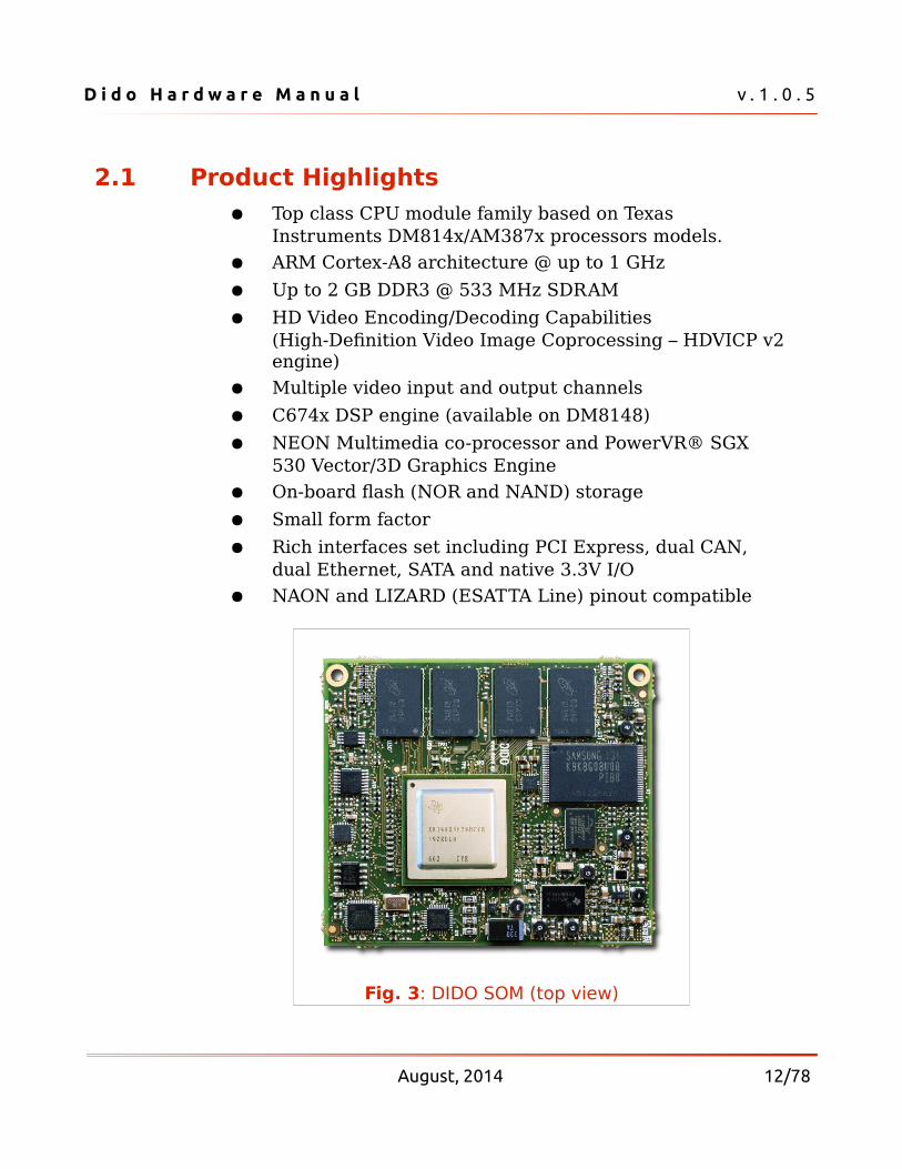
Fig. 3: DIDO SOM (top view)
D i d o H a r d w a r e M a n u a l v . 1 . 0 . 5
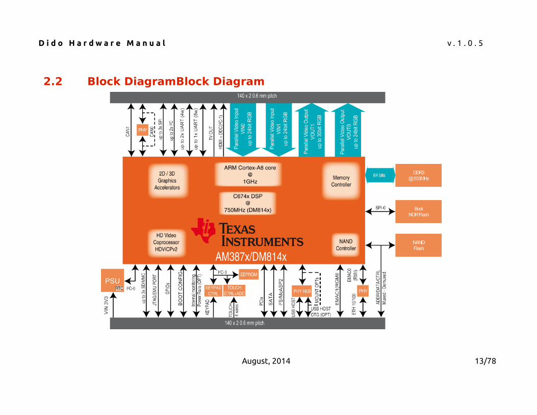
2.2 Block DiagramBlock Diagram
August, 2014 13/78
D i d o H a r d w a r e M a n u a l v . 1 . 0 . 5
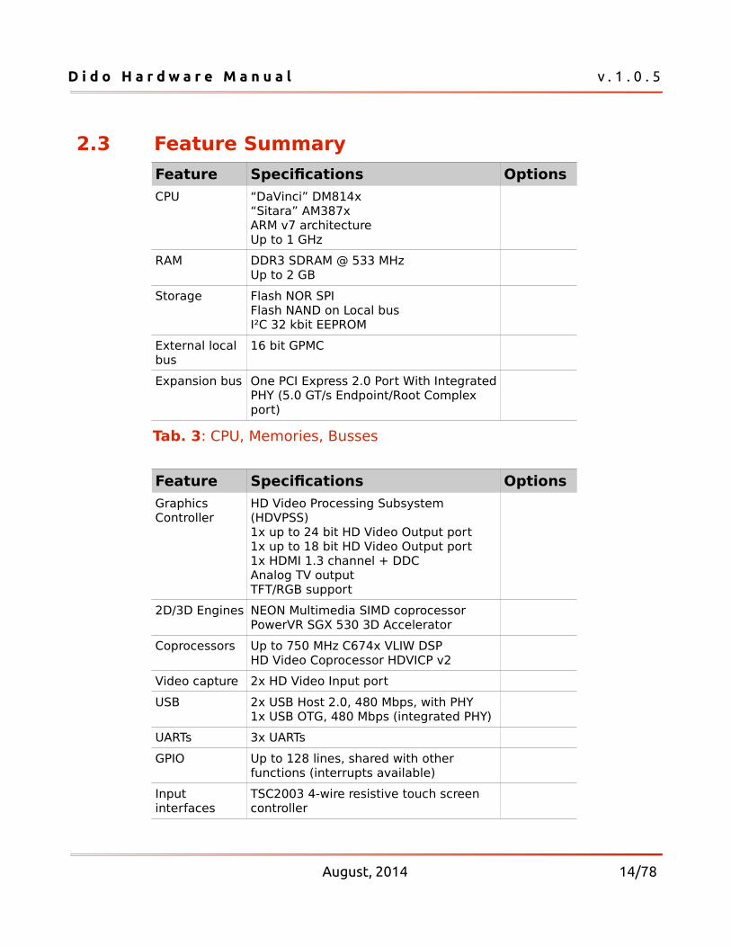
2.3 Feature Summary
Feature Specifications Options
CPU “DaVinci” DM814x“Sitara” AM387xARM v7 architectureUp to 1 GHz
RAM DDR3 SDRAM @ 533 MHzUp to 2 GB
Storage Flash NOR SPIFlash NAND on Local busI²C 32 kbit EEPROM
External local bus
16 bit GPMC
Expansion bus One PCI Express 2.0 Port With IntegratedPHY (5.0 GT/s Endpoint/Root Complex port)
Tab. 3: CPU, Memories, Busses
Feature Specifications Options
Graphics Controller
HD Video Processing Subsystem (HDVPSS)1x up to 24 bit HD Video Output port1x up to 18 bit HD Video Output port1x HDMI 1.3 channel + DDCAnalog TV outputTFT/RGB support
2D/3D Engines NEON Multimedia SIMD coprocessorPowerVR SGX 530 3D Accelerator
Coprocessors Up to 750 MHz C674x VLIW DSPHD Video Coprocessor HDVICP v2
Video capture 2x HD Video Input port
USB 2x USB Host 2.0, 480 Mbps, with PHY1x USB OTG, 480 Mbps (integrated PHY)
UARTs 3x UARTs
GPIO Up to 128 lines, shared with other functions (interrupts available)
Input interfaces
TSC2003 4-wire resistive touch screen controller
August, 2014 14/78
D i d o H a r d w a r e M a n u a l v . 1 . 0 . 5
Feature Specifications Options
Available ADC channelUp to 8x8 keypad controller
Networks 1x Fast Ethernet with PHY1x GRMII 10/100/1000 Mbps interfaceHigh-end Dual CAN controller
Storage Serial ATA 3.0 Gbps with integrated PHY
SD/MMC Up to 3x MMC/SD/SDIO Serial interfaces (up to 48 MHz)
Serial buses 2x I²C, 3x SPI
Audio 1x McASP channel
Timers Up to 6 programmable general purpose timers (PWM function available)
RTC On board (provided by TPS659113 PMIC), external battery powered
Debug JTAGEMU port
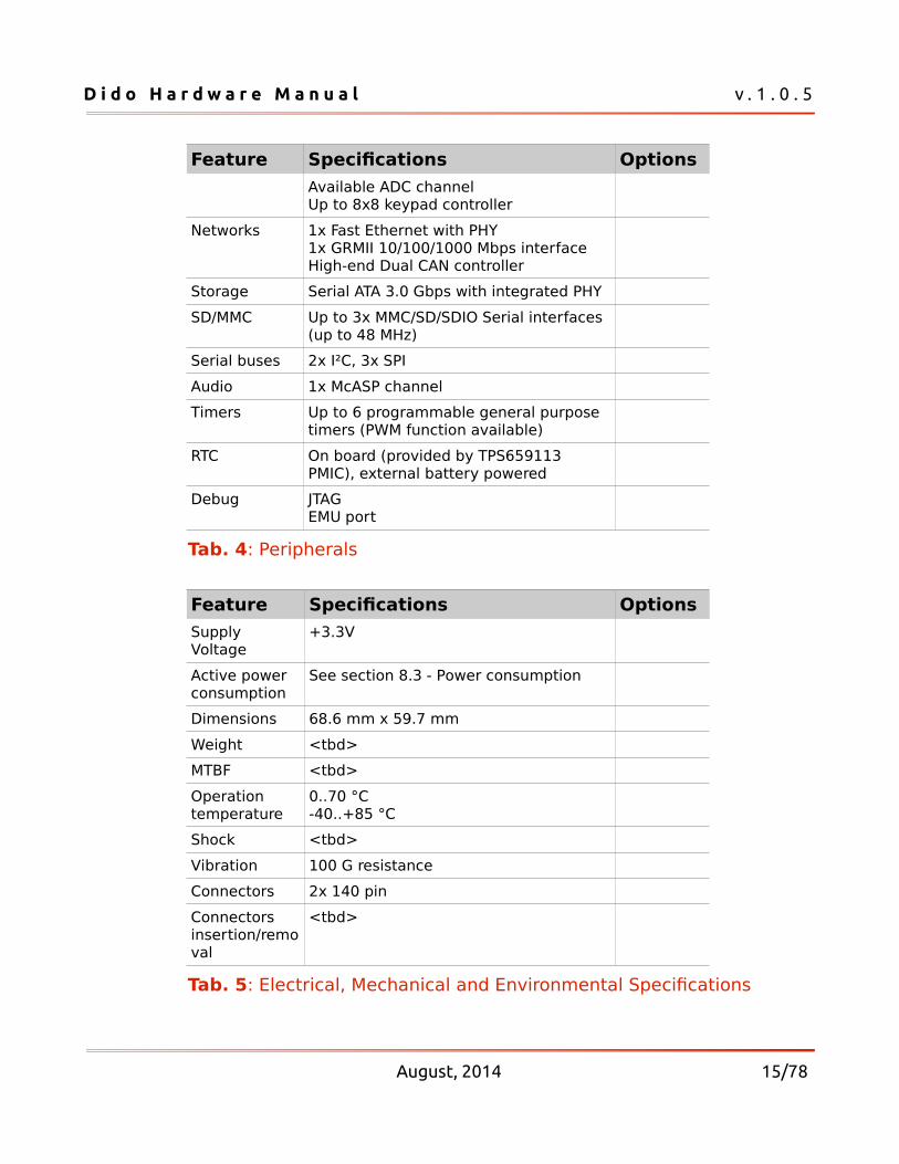
Tab. 4: Peripherals
Feature Specifications Options
Supply Voltage
+3.3V
Active power consumption
See section 8.3 - Power consumption
Dimensions 68.6 mm x 59.7 mm
Weight <tbd>
MTBF <tbd>
Operation temperature
0..70 °C-40..+85 °C
Shock <tbd>
Vibration 100 G resistance
Connectors 2x 140 pin
Connectors insertion/removal
<tbd>
Tab. 5: Electrical, Mechanical and Environmental Specifications
August, 2014 15/78
D i d o H a r d w a r e M a n u a l v . 1 . 0 . 5
3 Design overviewThe heart of DIDO module is composed by the following components:
Texas Instruments DM814x/AM387x processor
Power supply unit
DDR3 memory banks
NOR and NAND flash banks
2x 140 pin connectors with interfaces signals
This chapter shortly describes the main DIDO components.
3.1 “DaVinci” DM814x / “Sitara” AM387x CPUDM814x DaVinci™ and AM387x Sitara™ are highly-integrated, scalable and programmable CPU families from Texas Instruments.DaVinci™ digital media processor solutions are tailored for digital audio, video, imaging, and vision applications.Sitara™ ARM microprocessors (MPUs) are designed to optimize performance and peripheral support for customers in a variety of markets.The architecture is designed to provide video, image, graphics and processing power sufficient to support the following:
Home and Industrial automation
Test and measurement
Digital Signage
Medical instrumentation
Remote monitoring
Motion control
Point-of-Sale
Single Board Computers
The following subsystems are part of the device: Microprocessor unit (MPU) subsystem based on the ARM®
Cortex™-A8 architecture:
August, 2014 16/78
D i d o H a r d w a r e M a n u a l v . 1 . 0 . 5
ARM Cortex-A8 RISC processor, with Neon™ Floating-Point Unit, 32KB L1 Instruction Cache, 32KB L1Data Cache and 512KB L2 Cache
CoreSight Embedded Trace Module (ETM)
ARM Cortex-A8 Interrupt Controller (AINTC)
Embedded PLL Controller (PLL_ARM)
PowerVR SGX 530 subsystem for vector/3D graphics acceleration to support display and gaming effects
The HDVICP2 is a Video Encoder/Decoder hardware accelerator supporting a range of encode, decode, and transcode operations for most major video codec standards. The main video Codec standards supported in hardware are MPEG1/2/4 ASP/SP, H.264 BL/MP/HP, VC-1 SP/MP/AP, RV9/10, AVS-1.0, and ON2 VP6.2/VP7.
The C674x DSP core is the high-performance floating-point DSP generation in the TMS320C6000™ DSP platform and is code-compatible with previous generation C64x Fixed-Point and C67x Floating-Point DSP generation. The C674x Floating-Point DSP processor uses 32KB of L1 program memory with EDC and 32KB of L1 data memory. The DSP has 256KB of L2 RAM with ECC, which can be defined as SRAM, L2 cache, or a combination of both.
The high definition video processing subsystem (HDVPSS) includes video/graphics display and capture processing using the latest TI developed algorithms, flexible compositing and blending engine, and a full range of external video interfaces in order to deliver high quality video contents to the end devices.
The following table shows a comparison between the devices, highlighting the differences:
Processor DSP 3D HDVICP HDVPSS Max clock speed
DM8148 Yes Yes Yes Yes 1 GHz
DM8147 Yes n.a. Yes Yes 1 GHz
August, 2014 17/78
D i d o H a r d w a r e M a n u a l v . 1 . 0 . 5
Processor DSP 3D HDVICP HDVPSS Max clock speed
AM3874 n.a. Yes n.a. Yes 1 GHz
AM3872 n.a. n.a. n.a. Yes 1 GHz
AM3871 n.a. n.a. n.a. n.a. 1 GHz
Tab. 6: DM814x/AM387x comparison
3.2 DDR3 memory bankDDR3 SDRAM memory bank is composed by 4x 16-bit width chips resulting in 2x 32-bit combined width banks.
The following table reports the SDRAM specifications:
CPU connection SDRAM bus
Size min 128 MB
Size max 2 GB
Width 32 bit
Speed 533 MHz
Tab. 7: DDR2 specifications
3.3 NOR flash bankNOR flash is a Serial Peripheral Interface (SPI) device. By default this device is connected to SPI channel 0 and acts as boot memory.The following table reports the NOR flash specifications:
CPU connection SPI channel 0
Size min 4 MByte
Size max 128 MByte
Bootable Yes
Tab. 8: NOR flash specifications
3.4 NAND flash bankOn board main storage memory is a 8-bit wide NAND flash. By default it is connected to GPMC_NCS0 chip select. Optionally it
August, 2014 18/78
D i d o H a r d w a r e M a n u a l v . 1 . 0 . 5
can be connected to GPMC_NCS7.
CPU connection GPMC bus
Page size 512 byte, 2 kbyte or 4 kbyte
Size min 32 MByte
Size max 2 GByte
Width 8 bit
Bootable Yes
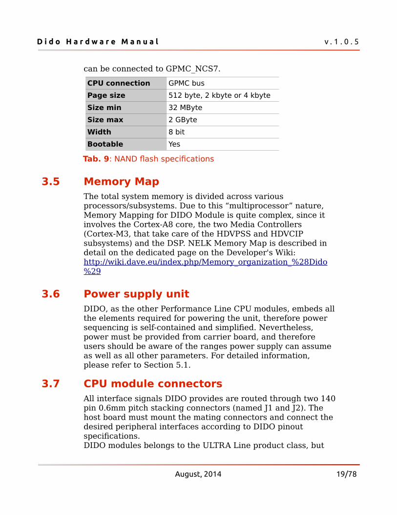
Tab. 9: NAND flash specifications
3.5 Memory MapThe total system memory is divided across various processors/subsystems. Due to this “multiprocessor” nature, Memory Mapping for DIDO Module is quite complex, since it involves the Cortex-A8 core, the two Media Controllers (Cortex-M3, that take care of the HDVPSS and HDVCIP subsystems) and the DSP. NELK Memory Map is described in detail on the dedicated page on the Developer's Wiki: http://wiki.dave.eu/index.php/Memory_organization_%28Dido%29
3.6 Power supply unitDIDO, as the other Performance Line CPU modules, embeds all the elements required for powering the unit, therefore power sequencing is self-contained and simplified. Nevertheless, power must be provided from carrier board, and therefore users should be aware of the ranges power supply can assume as well as all other parameters. For detailed information, please refer to Section 5.1.
3.7 CPU module connectorsAll interface signals DIDO provides are routed through two 140pin 0.6mm pitch stacking connectors (named J1 and J2). The host board must mount the mating connectors and connect the desired peripheral interfaces according to DIDO pinout specifications.DIDO modules belongs to the ULTRA Line product class, but
August, 2014 19/78
D i d o H a r d w a r e M a n u a l v . 1 . 0 . 5
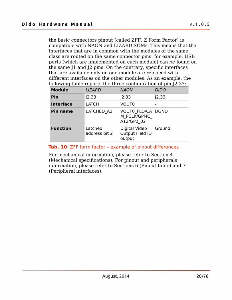
the basic connectors pinout (called ZFF, Z Form Factor) is compatible with NAON and LIZARD SOMs. This means that theinterfaces that are in common with the modules of the same class are routed on the same connector pins: for example, USB ports (which are implemented on each module) can be found onthe same J1 and J2 pins. On the contrary, specific interfaces that are available only on one module are replaced with different interfaces on the other modules. As an example, the following table reports the three configuration of pin J2.33:Module LIZARD NAON DIDO
Pin J2.33 J2.33 J2.33
Interface LATCH VOUT0 -
Pin name LATCHED_A2 VOUT0_FLD/CAM_PCLK/GPMC_A12/GP2_02
DGND
Function Latched address bit 2
Digital Video Output Field IDoutput
Ground
Tab. 10: ZFF form factor – example of pinout differences
For mechanical information, please refer to Section 4 (Mechanical specifications). For pinout and peripherals information, please refer to Sections 6 (Pinout table) and 7 (Peripheral interfaces).
August, 2014 20/78
D i d o H a r d w a r e M a n u a l v . 1 . 0 . 5
4 Mechanical specificationsThis chapter describes the mechanical characteristics of the DIDO module.
Mechanical drawings are available in DXF format from the DIDO page on DAVE Embedded Systems website (http://www.dave.eu/dave-cpu-module-am387x-dm814x-dido.html).
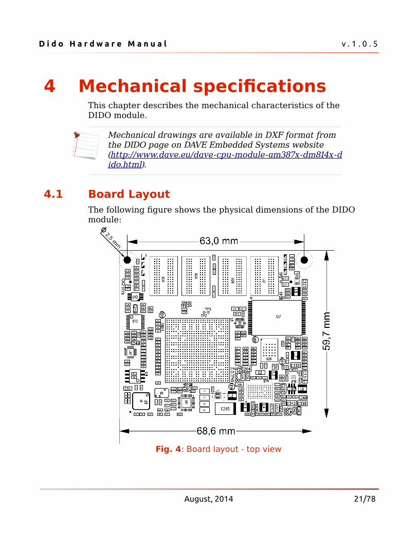
4.1 Board LayoutThe following figure shows the physical dimensions of the DIDOmodule:
August, 2014 21/78
Fig. 4: Board layout - top view
D i d o H a r d w a r e M a n u a l v . 1 . 0 . 5
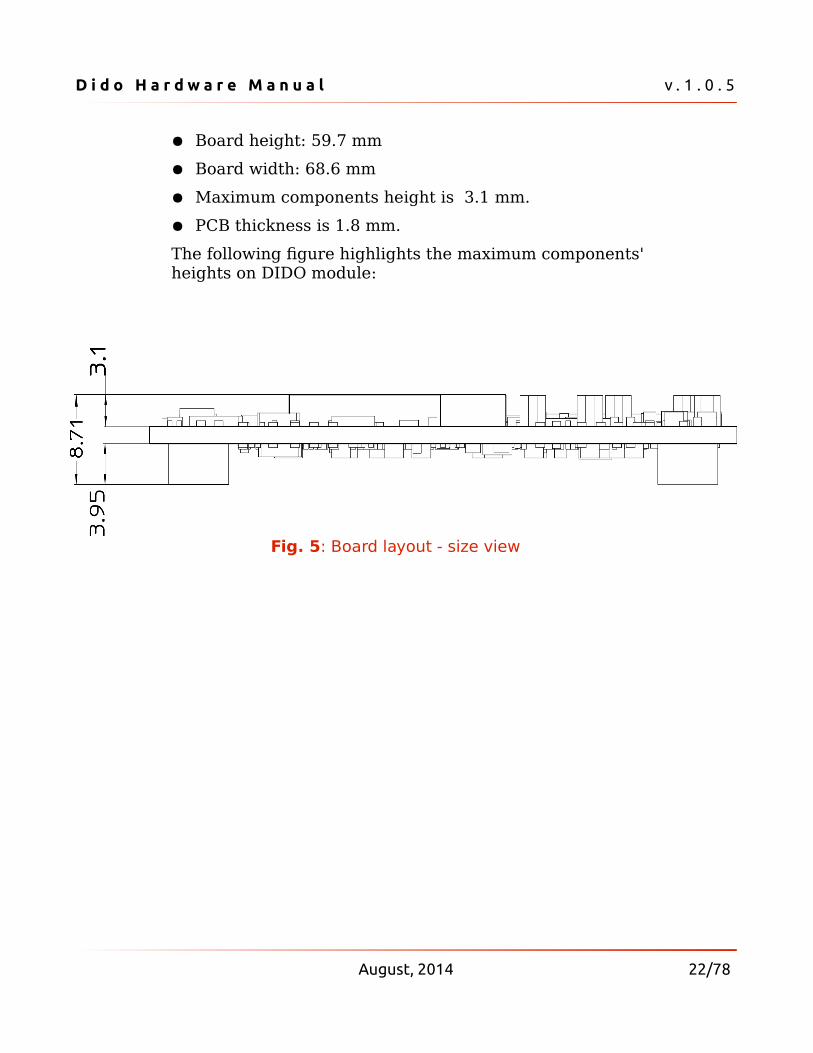
Board height: 59.7 mm
Board width: 68.6 mm
Maximum components height is 3.1 mm.
PCB thickness is 1.8 mm.
The following figure highlights the maximum components' heights on DIDO module:
August, 2014 22/78
Fig. 5: Board layout - size view

D i d o H a r d w a r e M a n u a l v . 1 . 0 . 5
4.2 ConnectorsThe following figure shows the DIDO connectors layout:
The following table reports connectors specifications:
Part number Hirose FX8C-140S-SV
Height 5.6 mm
Length 48.6 mm
Depth 3.95 mm
Mating connectors
Hirose FX8C-140P-SV (5 mm board-to-board height)Hirose FX8C-140P-SV1 (6 mm board-to-board height)Hirose FX8C-140P-SV2 (7 mm board-to-board height)Hirose FX8C-140P-SV4 (9 mm board-to-board height)Hirose FX8C-140P-SV6 (11 mm board-to-board height)
August, 2014 23/78
Fig. 6: Connectors layout
D i d o H a r d w a r e M a n u a l v . 1 . 0 . 5
5 System Logic
5.1 PowerImplementing correct power-up sequence for AM387x/DM814x processor is not a trivial task because several power rails are involved. DIDO hides this complexity because it embeds most of the circuitry required.In typical applications AM387x/DM814x processor interfaces directly to 3.3V-powered devices that are hosted on carrier board. In order to be compliant with AM387x/DM814x power-up requirements, these devices should be turned on at a specific time during power-up sequence. To achieve this, DIDO provides EN_BCK2_LS signal. When DIDO is powered, this signal is low: this means that carrier board 3.3V-powered devices have to be powered off. During power-up sequence thissignal shall be raised by DIDO circuitry, indicating carrier board 3.3V-powered devices have to be turned on. After this rising edge, EN_BCK2_LS shall be kept high.
5.2 PMICThis section will be completed in a future version of this manual.
5.3 ResetFive different signals are provided by DIDO SOM. Following sections describes in more detail each one.
5.3.1 MRST (J2.102)This pin is connected to HDRST signal (cold reset) of PMIC TPS659113. When high, this signals keeps PMIC in off mode and resets TPS659113 to default settings. MRST has a weak internal pulldown.
5.3.2 PORSTn (J2.109)PORSTn is a bidirectional open-drain signal. It is connected to:
August, 2014 24/78
D i d o H a r d w a r e M a n u a l v . 1 . 0 . 5
PORn input (Power-on Reset) of DM8148 processor
output of voltage monitor (see Section 5.4)
NRESPWRON2 output of PMIC.
Internal pullup is 10kOhm.
5.3.3 RSTOUTn (J2.91)This output signal is asserted by DM8148 processor until it gets out of reset. It is usually used to reset external memories and peripherals connected to processor. It is connected to:
RSTOUT_WD_OUTn pad of DM8148 processor
2k2 pull down resistor
peripherals and memories.
In case it is used to reset devices on carrier board, its driving capability has to be taken into account.
5.3.4 CPU_RESETn (J2.15)This input signal acts as External Warm Reset. It is connected to processor's RESETn pad. Internal pullup is 2.2kOhm.
5.3.5 JTAG_TRSTn (J2.100)This input signal acts as Emulation Warm Reset. It is connectedto processor's TRSTn pad. Internal pulldown is 4.7kOhm
5.4 Voltage monitorDIDO SOM is equipped with a multiple-input voltage monitor whose reset output is connected to PORSTn. Monitored voltagerails include 3.3V provided by carrier board.
5.5 Boot optionsThanks to the versatility of internal BootROM, DM814x/AM387x processors provide a rich set of boot options and different configurations selectable via BTMODE[15:0] bootstrap pins. For a detailed explanation on the boot process for DM814x/AM387x processors, please refer to the Technical Reference Manual (available from TI website) at section ROM
August, 2014 25/78
D i d o H a r d w a r e M a n u a l v . 1 . 0 . 5
Code Memory and Peripheral Booting. In order to fully understand how boot work on DIDO platform, please refer to Section 3.5 (Memory Map).
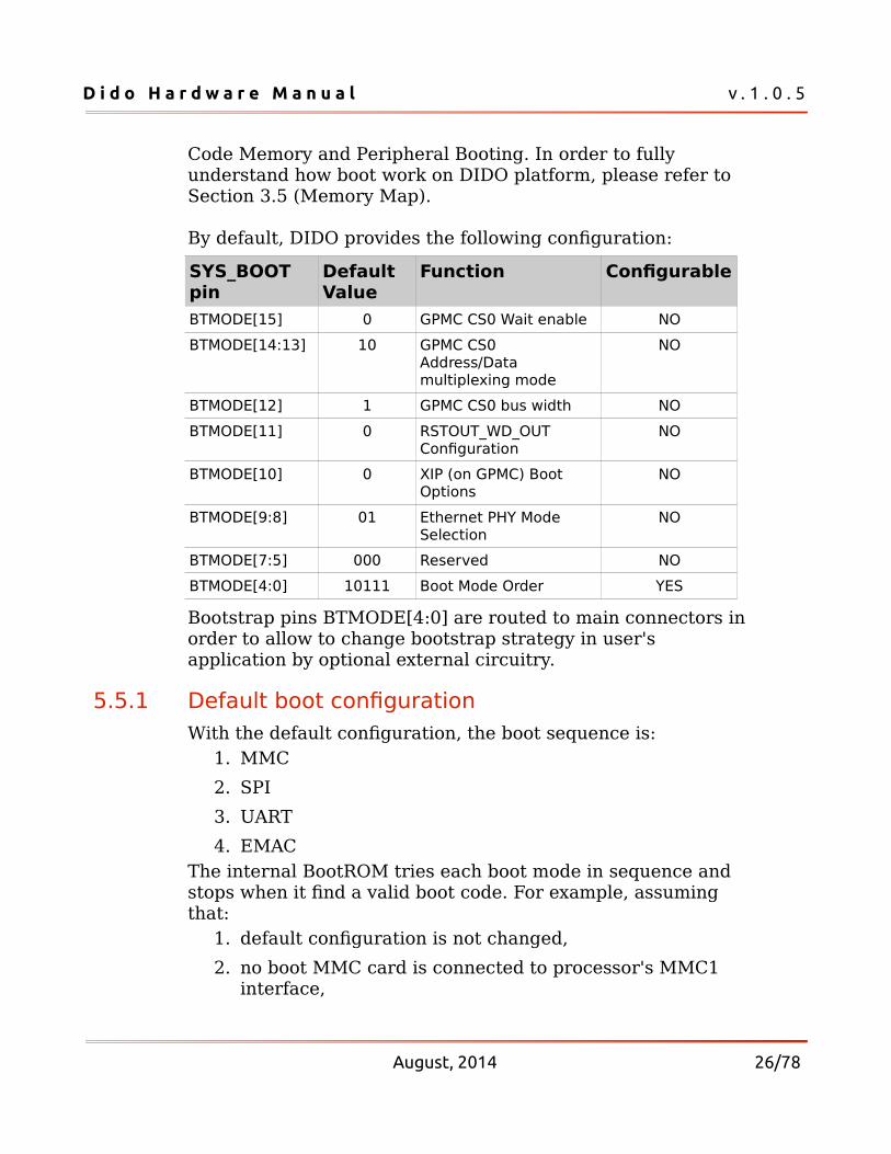
By default, DIDO provides the following configuration:
SYS_BOOT pin
Default Value
Function Configurable
BTMODE[15] 0 GPMC CS0 Wait enable NO
BTMODE[14:13] 10 GPMC CS0 Address/Data multiplexing mode
NO
BTMODE[12] 1 GPMC CS0 bus width NO
BTMODE[11] 0 RSTOUT_WD_OUT Configuration
NO
BTMODE[10] 0 XIP (on GPMC) Boot Options
NO
BTMODE[9:8] 01 Ethernet PHY Mode Selection
NO
BTMODE[7:5] 000 Reserved NO
BTMODE[4:0] 10111 Boot Mode Order YES
Bootstrap pins BTMODE[4:0] are routed to main connectors in order to allow to change bootstrap strategy in user's application by optional external circuitry.
5.5.1 Default boot configurationWith the default configuration, the boot sequence is:
1. MMC
2. SPI
3. UART
4. EMACThe internal BootROM tries each boot mode in sequence and stops when it find a valid boot code. For example, assuming that:
1. default configuration is not changed,
2. no boot MMC card is connected to processor's MMC1 interface,
August, 2014 26/78
D i d o H a r d w a r e M a n u a l v . 1 . 0 . 5
3. and there's a valid boot code programmed in SPI memorythe boot sequence performed by ARM core will be:
1. execute bootrom from internal ROM code memory
2. launch 1st stage bootloader
• copied from on-board NOR flash memory connected toSPI0 port to on-chip SRAM by bootrom
• executed from on-chip SRAM
3. launch 2nd stage bootloader
• copied by 1st stage bootloader from NOR flash memoryconnected to SPI0 port to SDRAM
• executed from SDRAM
If no boot code is available in SPI NOR flash (for the bootrom this means that the first sector read returns 0xFFFFFFFF) the bootrom tries UART (please see also Section 5.7) and EMAC peripheral booting.
5.5.2 Boot sequence customizationThe following reference schematic shows a simple resistor network that can be implemented on carrier board hosting DIDO module. For each BTMODE[4:0] pin it is possible to populate upper or lower side resistor in order to change defaultvalue that is set on module itself. The available boot mode orders are reported in Table 4-8. “BTMODE[4-0] Configuration Pins” in Section 4 “ROM Code Memory and Peripheral Booting”of the DM814x/AM387x Technical Reference Manual.
5.6 Clock schemeThis section will be completed in a future version of this manual.
5.7 RecoveryFor different reason, starting from image corruption due powerloss during upgrade or unrecoverable bug while developing a new U-Boot feature, the user will need, sooner or later, to recover (bare-metal restore) the DIDO SOM without using the bootloader itself. The following paragraphs introduce the
August, 2014 27/78
D i d o H a r d w a r e M a n u a l v . 1 . 0 . 5
available options. For further information, please refer to DAVEEmbedded Systems Developers Wiki or contact the Technical Support Team.
5.7.1 JTAG RecoveryJTAG recovery, though very useful (especially in development or production environment), requires dedicated hardware and software tools. DIDO provides the JTAG interface, which, besides the debug purpose, can be used for programming and recovery operations. For further information on how to use the JTAG interface, please contact the Technical Support Team.
5.7.2 UART RecoveryUART recovery does not requires any specialized hardware, apart a PC and a DB9 serial cross cable. The boot sequence must include the UART option and a way to enable it. Then a simple procedure allow to load the 1st and 2nd stage bootloader from the serial line. When the 2nd stage bootloader is running, reprogramming the flash memory is straightforward.
The UART boot uses UART0 interface.
5.7.3 SD/MMC RecoveryMMC recovery is a valuable options that requires no special hardware at all, apart a properly formatted MMC. The boot sequence must include the SD/MMC option and a way to enableit. When SD/MMC boot option is selected, bootrom looks for a valid boot sector on SD/MMC1. Once the board is running afterbooting from SD, reprogramming the flash memory is straightforward.
5.8 MultiplexingDM814x/AM387x pins can have up to seven alternate function modes. The I/O pins can be internally routed to/from one of several peripheral modules within the device: this routing is referred to as Pin Multiplexing. Pin Multiplexing allows software to choose the subset of internal signals which will be
August, 2014 28/78
D i d o H a r d w a r e M a n u a l v . 1 . 0 . 5
mapped to balls of the device for a given application. Pin multiplexing selects which one of several peripheral pin functions controls the pin's I/O buffer output data values.
Please note that pin mux configuration is a very critical step. Wrong configuration may lead to system instability, side effects or even damage the hardware permanently
Pin multiplexing configuration is quite complex in DIDO but a tool from TI, the Pin Mux Utility, can help to perform this operation. Software installation and generic usage documentation is available on this page of the TI Embedded Processors Wiki: http://processors.wiki.ti.com/index.php/Pin_Mux_Utility_for_ARM_MPU_Processors
5.9 RTCThe TPS659113 PMIC provides a real-time clock (RTC) resource with Oscillator for 32.768-kHz crystal
Date, time and calendar
Alarm capability
Backup power from external battery
Backup power is provided through the VBAT (J1.9) signal. If notused, VBAT must be externally connected to GND.
August, 2014 29/78
D i d o H a r d w a r e M a n u a l v . 1 . 0 . 5
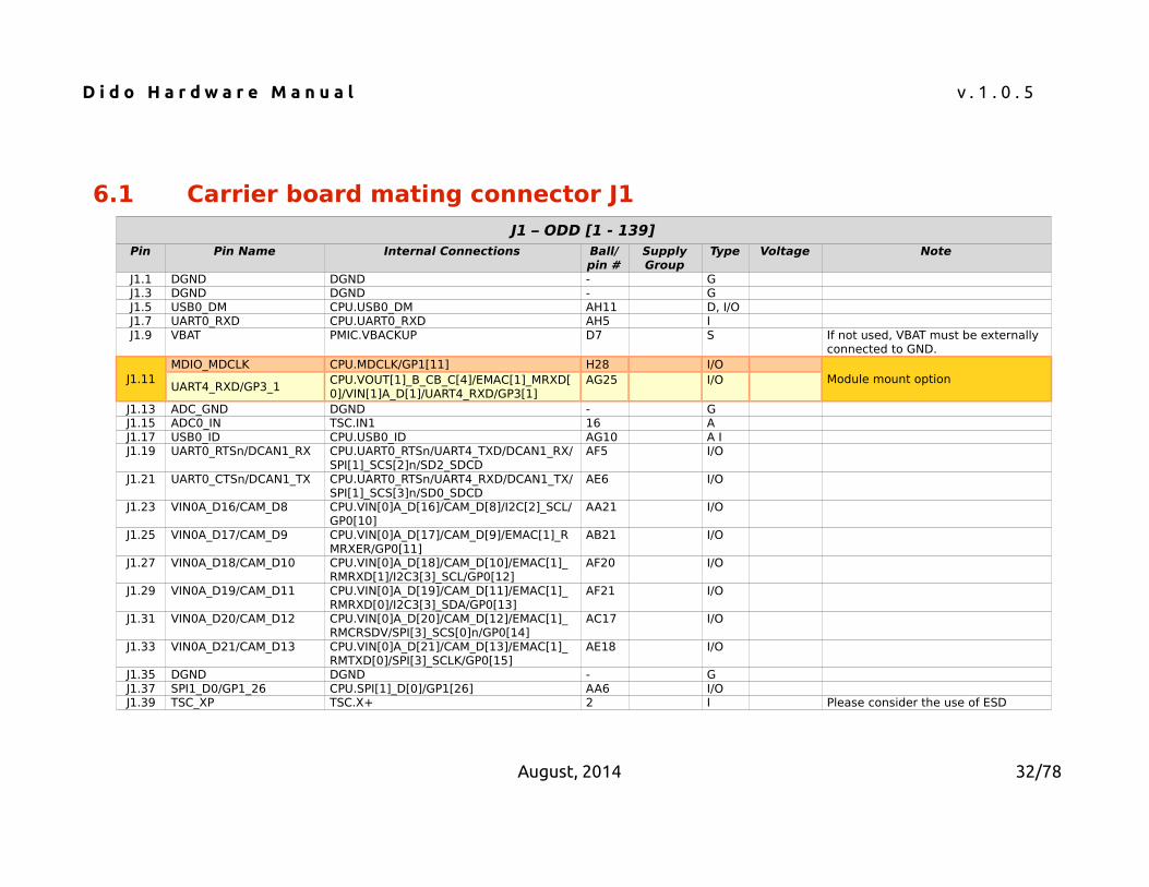
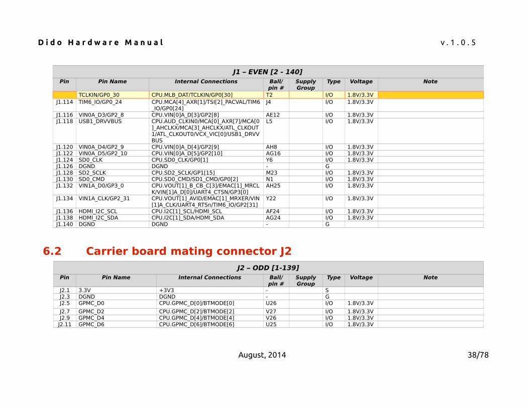
6 Pinout tableThis chapter contains the pinout description of the DIDO module, grouped in four tables (two – odd and even pins – for each connector) that report the pin mapping of the two 140 pinDIDO connectors.Each row in the pinout tables contains the following information:Pin Reference to the connector pin
Pin Name Pin (signal) name on the DIDO connectors
Internal Connections
Connections to the DIDO components:CPU.<x> : pin connected to CPU pad named <x>KEY.<x>: pin connected to the key switch controllerTSC.<x> : pin connected to the touchscreen controllerEEPROM.<x> : pin connected to the EEPROMCAN.<x> : pin connected to the CAN transceiverPMIC.<x> : pin connected to the Power Manager ICLAN.<x> : pin connected to the LAN PHYUSB.<x> : pin connected to the USB transceiverSV.<x>: pin connected to voltage supervisorMTR: pin connected to voltage monitors
Ball/pin # Component ball/pin number connected to signal
Supply Group Power Supply Group
Type Pin type: I = Input, O = Output, D= Differential, Z = High impedance, S = Supply voltage, G = Ground, A = Analog signal
Voltage I/O voltage
The Internal connection column reports the name of the microprocessor signal, which in turn contains references to all the peripheral functions that can be associated to that pin. For example, the following pin nameCPU.VOUT[1]_B_CB_C[4]/EMAC[1]_MRXD[0]/VIN[1]A_D[1]/UART4_RXD/GP3[1]means that the pin can be used as: VOUT[1]_B_CB_C[4]: Video output data, port 1, B/CB/C
color bit 4
August, 2014 30/78

D i d o H a r d w a r e M a n u a l v . 1 . 0 . 5
EMAC[1]_MRXD[0]: Ethernet MAC, port 1, [G]MII Receive Data, bit 0
VIN[1]A_D[1]: Video input channel 1, port A data input bit 1 UART[4]_RXD: UART port 4, receive data input GP3[1]: General Purpose I/O port 3, channel 1The following table reports all the function names that can be found on the Internal connection and the associated description.Functionname
Description
VOUT[x] Digital video output. “x” represents the port number (0 or 1).
VIN[x]A/B Digital video input. “x” represents the capture number (0 or 1). Each capture has two ports (A and B)
EMAC[x] Ethernet MAC. “x” represents the port number (0 or 1)
UART[x] UART port. “x” represents the port number (0 to 5)
GPx[y] General Purpose I/O port. “x” represents the port number (0 to 3)
CAM Camera Interface
SPI[x] SPI channel. “x” represents the channel number (0 to 3)
DCAN[x] Controller Area Network module. “x” represents the module number (0 to 1)
HDMI High-Definition Multimedia Interface
SD[x] MMC/SD/SDIO interfaces. “x” represents the interface number (0 to 2)
GPMC General Purpose Memory Controller (local bus)
MD Management Data I/O module
MCA[x] Multi-Channel Audio Serial Port (McASP). “x” represents the port number (0 to 5)
I2C[x] I2C channel. “x” represents the channel number (0 to 3)
AUD Audio Reference Clock
TIMx General purpose timer. “x” represents the terminal number (0 to 7)
August, 2014 31/78
D i d o H a r d w a r e M a n u a l v . 1 . 0 . 5
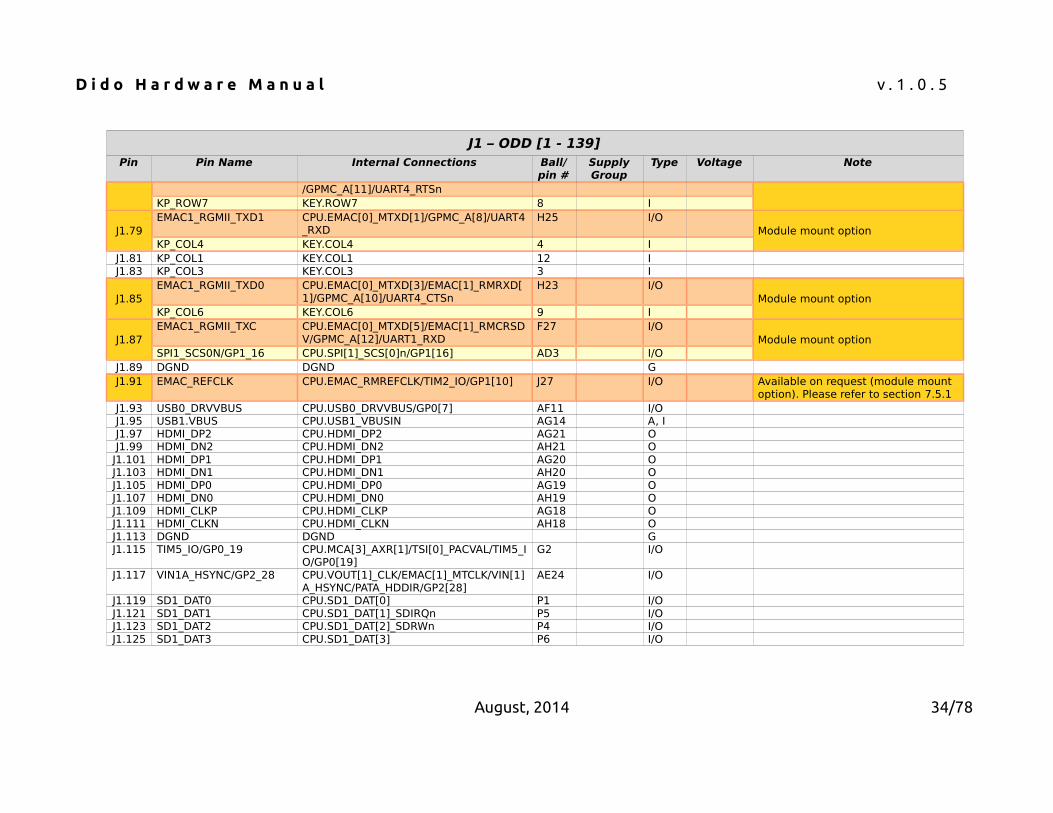
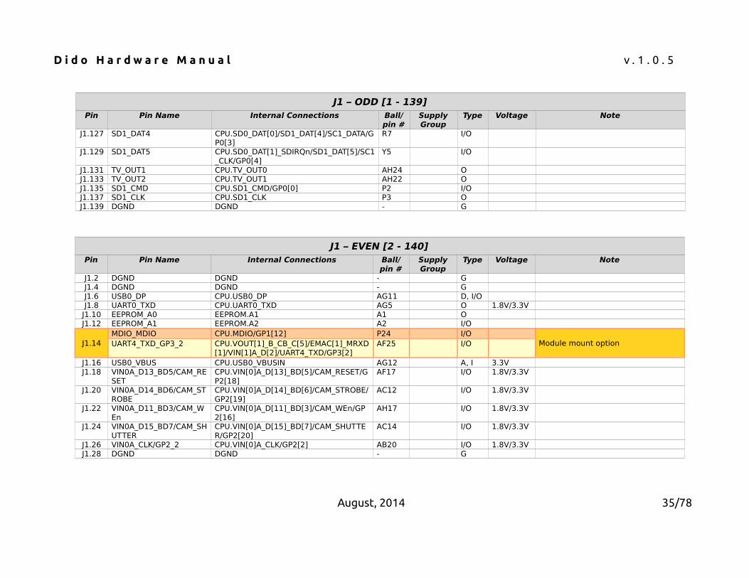
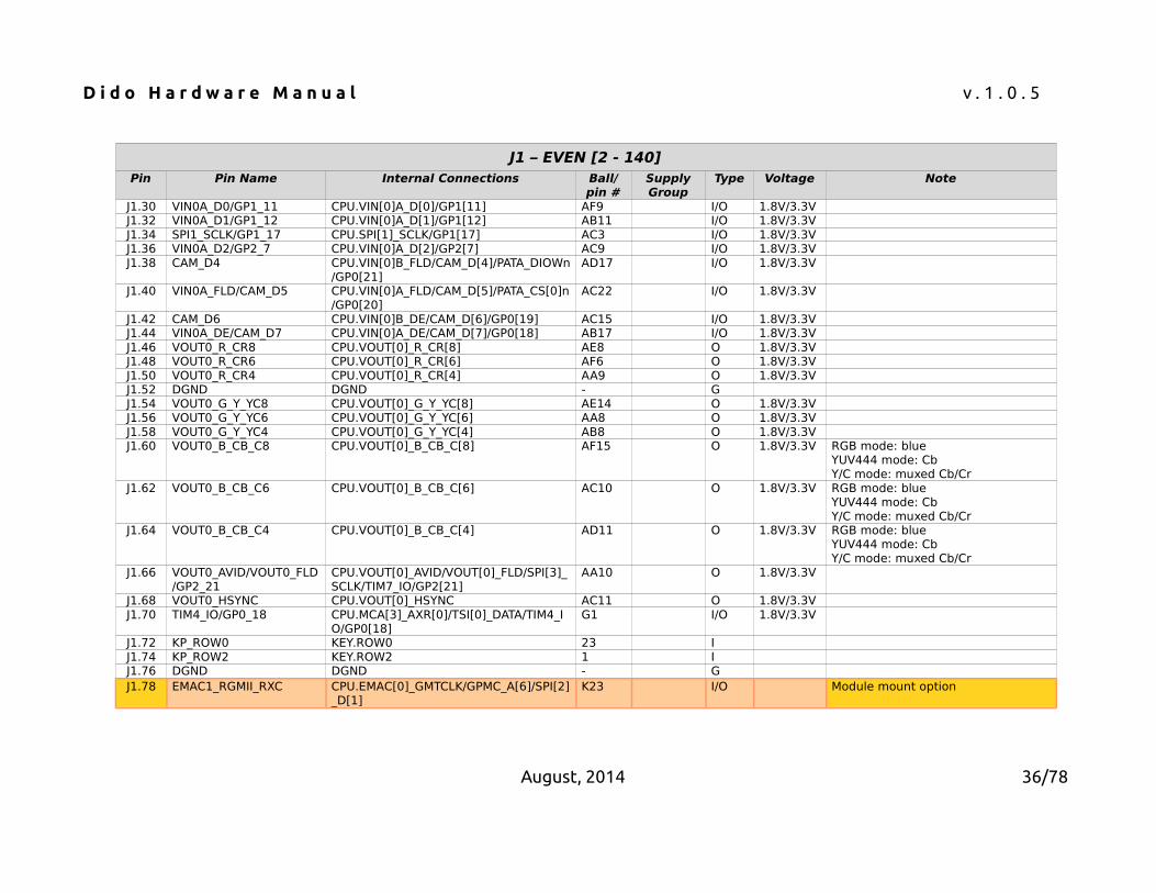
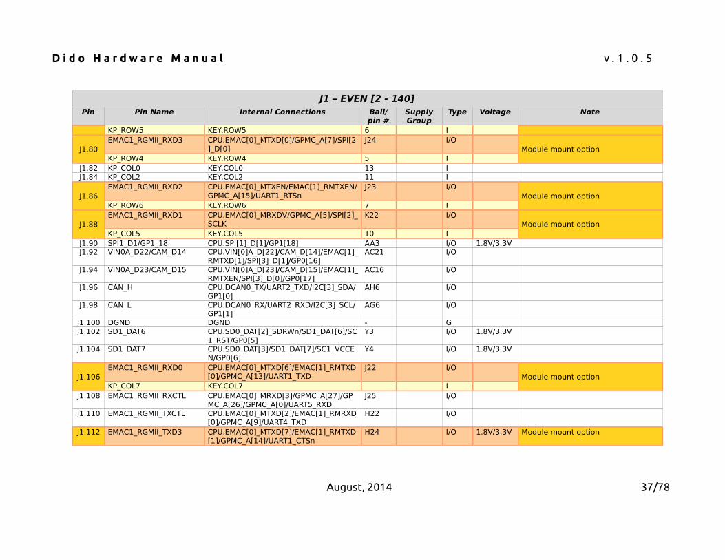
6.1 Carrier board mating connector J1J1 – ODD [1 - 139]
Pin Pin Name Internal Connections Ball/pin #
SupplyGroup
Type Voltage Note
J1.1 DGND DGND - GJ1.3 DGND DGND - GJ1.5 USB0_DM CPU.USB0_DM AH11 D, I/OJ1.7 UART0_RXD CPU.UART0_RXD AH5 IJ1.9 VBAT PMIC.VBACKUP D7 S If not used, VBAT must be externally
connected to GND.
J1.11MDIO_MDCLK CPU.MDCLK/GP1[11] H28 I/O
Module mount optionUART4_RXD/GP3_1
CPU.VOUT[1]_B_CB_C[4]/EMAC[1]_MRXD[0]/VIN[1]A_D[1]/UART4_RXD/GP3[1]
AG25 I/O
J1.13 ADC_GND DGND - GJ1.15 ADC0_IN TSC.IN1 16 AJ1.17 USB0_ID CPU.USB0_ID AG10 A IJ1.19 UART0_RTSn/DCAN1_RX CPU.UART0_RTSn/UART4_TXD/DCAN1_RX/
SPI[1]_SCS[2]n/SD2_SDCDAF5 I/O
J1.21 UART0_CTSn/DCAN1_TX CPU.UART0_RTSn/UART4_RXD/DCAN1_TX/SPI[1]_SCS[3]n/SD0_SDCD
AE6 I/O
J1.23 VIN0A_D16/CAM_D8 CPU.VIN[0]A_D[16]/CAM_D[8]/I2C[2]_SCL/GP0[10]
AA21 I/O
J1.25 VIN0A_D17/CAM_D9 CPU.VIN[0]A_D[17]/CAM_D[9]/EMAC[1]_RMRXER/GP0[11]
AB21 I/O
J1.27 VIN0A_D18/CAM_D10 CPU.VIN[0]A_D[18]/CAM_D[10]/EMAC[1]_RMRXD[1]/I2C3[3]_SCL/GP0[12]
AF20 I/O
J1.29 VIN0A_D19/CAM_D11 CPU.VIN[0]A_D[19]/CAM_D[11]/EMAC[1]_RMRXD[0]/I2C3[3]_SDA/GP0[13]
AF21 I/O
J1.31 VIN0A_D20/CAM_D12 CPU.VIN[0]A_D[20]/CAM_D[12]/EMAC[1]_RMCRSDV/SPI[3]_SCS[0]n/GP0[14]
AC17 I/O
J1.33 VIN0A_D21/CAM_D13 CPU.VIN[0]A_D[21]/CAM_D[13]/EMAC[1]_RMTXD[0]/SPI[3]_SCLK/GP0[15]
AE18 I/O
J1.35 DGND DGND - GJ1.37 SPI1_D0/GP1_26 CPU.SPI[1]_D[0]/GP1[26] AA6 I/OJ1.39 TSC_XP TSC.X+ 2 I Please consider the use of ESD
August, 2014 32/78

D i d o H a r d w a r e M a n u a l v . 1 . 0 . 5
J1 – ODD [1 - 139]Pin Pin Name Internal Connections Ball/
pin #SupplyGroup
Type Voltage Note
protection devices on carrier board when these pins are connected to actual touch screen.
J1.41 TSC_XM TSC.X- 4 IJ1.43 TSC_YP TSC.Y+ 3 IJ1.45 TSC_YM TSC.Y- 5 IJ1.47 VOUT0_R_CR9 CPU.VOUT[0]_R_CR[9] AC13 O RGB mode: red
YUV444 mode: CrJ1.49 VOUT0_R_CR7 CPU.VOUT[0]_R_CR[7] AF12 O RGB mode: red
YUV444 mode: CrJ1.51 VOUT0_R_CR5 CPU.VOUT[0]_R_CR[5] AF8 O RGB mode: red
YUV444 mode: CrJ1.53 VOUT0_G_Y_YC9 CPU.VOUT[0]_G_Y_YC[9] AF14 O RGB mode: green
YUV444 mode: YY/C mode: Y
J1.55 VOUT0_G_Y_YC7 CPU.VOUT[0]_G_Y_YC[7] AD14 O RGB mode: greenYUV444 mode: YY/C mode: Y
J1.57 VOUT0_G_Y_YC5 CPU.VOUT[0]_G_Y_YC[5] AB12 O RGB mode: greenYUV444 mode: YY/C mode: Y
J1.59 VOUT0_B_CB_C9 CPU.VOUT[0]_B_CB_C[9] AG15 O RGB mode: blueYUV444 mode: CbY/C mode: muxed Cb/Cr
J1.61 VOUT0_B_CB_C7 CPU.VOUT[0]_B_CB_C[7] AB10 O RGB mode: blueYUV444 mode: CbY/C mode: muxed Cb/Cr
J1.63 DGND DGND - GJ1.65 VOUT0_B_CB_C5 CPU.VOUT[0]_B_CB_C[5] AD15 O RGB mode: blue
YUV444 mode: CbY/C mode: muxed Cb/Cr
J1.67 TIM2_IO/GP0_8 CPU.AUD_CLKIN1/MCA[0]_AXR[8]/MCA[1]_AHCLKX/MCA[4]_AHCLKX/ATL_CLKOUT2/EDMA_EVT3/TIM2_IO/GP0[8]
R5 I/O
J1.69 VOUT0_VSYNC CPU.VOUT[0]_VSYNC AB13 OJ1.71 VOUT0_CLK CPU.VOUT[0]_CLK AD12 OJ1.73 KP_ROW1 KEY.ROW1 24 IJ1.75 KP_ROW3 KEY.ROW3 2 IJ1.77 EMAC1_RGMII_TXD2 CPU.EMAC[0]_MTXD[4]/EMAC[1]_RMRXER G23 I/O Module mount option
August, 2014 33/78
D i d o H a r d w a r e M a n u a l v . 1 . 0 . 5
J1 – ODD [1 - 139]Pin Pin Name Internal Connections Ball/
pin #SupplyGroup
Type Voltage Note
/GPMC_A[11]/UART4_RTSnKP_ROW7 KEY.ROW7 8 I
J1.79EMAC1_RGMII_TXD1 CPU.EMAC[0]_MTXD[1]/GPMC_A[8]/UART4
_RXDH25 I/O
Module mount optionKP_COL4 KEY.COL4 4 I
J1.81 KP_COL1 KEY.COL1 12 IJ1.83 KP_COL3 KEY.COL3 3 I
J1.85EMAC1_RGMII_TXD0 CPU.EMAC[0]_MTXD[3]/EMAC[1]_RMRXD[
1]/GPMC_A[10]/UART4_CTSnH23 I/O
Module mount optionKP_COL6 KEY.COL6 9 I
J1.87EMAC1_RGMII_TXC CPU.EMAC[0]_MTXD[5]/EMAC[1]_RMCRSD
V/GPMC_A[12]/UART1_RXDF27 I/O
Module mount optionSPI1_SCS0N/GP1_16 CPU.SPI[1]_SCS[0]n/GP1[16] AD3 I/O
J1.89 DGND DGND GJ1.91 EMAC_REFCLK CPU.EMAC_RMREFCLK/TIM2_IO/GP1[10] J27 I/O Available on request (module mount
option). Please refer to section 7.5.1J1.93 USB0_DRVVBUS CPU.USB0_DRVVBUS/GP0[7] AF11 I/OJ1.95 USB1.VBUS CPU.USB1_VBUSIN AG14 A, IJ1.97 HDMI_DP2 CPU.HDMI_DP2 AG21 OJ1.99 HDMI_DN2 CPU.HDMI_DN2 AH21 OJ1.101 HDMI_DP1 CPU.HDMI_DP1 AG20 OJ1.103 HDMI_DN1 CPU.HDMI_DN1 AH20 OJ1.105 HDMI_DP0 CPU.HDMI_DP0 AG19 OJ1.107 HDMI_DN0 CPU.HDMI_DN0 AH19 OJ1.109 HDMI_CLKP CPU.HDMI_CLKP AG18 OJ1.111 HDMI_CLKN CPU.HDMI_CLKN AH18 OJ1.113 DGND DGND GJ1.115 TIM5_IO/GP0_19 CPU.MCA[3]_AXR[1]/TSI[0]_PACVAL/TIM5_I
O/GP0[19]G2 I/O
J1.117 VIN1A_HSYNC/GP2_28 CPU.VOUT[1]_CLK/EMAC[1]_MTCLK/VIN[1]A_HSYNC/PATA_HDDIR/GP2[28]
AE24 I/O
J1.119 SD1_DAT0 CPU.SD1_DAT[0] P1 I/OJ1.121 SD1_DAT1 CPU.SD1_DAT[1]_SDIRQn P5 I/OJ1.123 SD1_DAT2 CPU.SD1_DAT[2]_SDRWn P4 I/OJ1.125 SD1_DAT3 CPU.SD1_DAT[3] P6 I/O
August, 2014 34/78
D i d o H a r d w a r e M a n u a l v . 1 . 0 . 5
J1 – ODD [1 - 139]Pin Pin Name Internal Connections Ball/
pin #SupplyGroup
Type Voltage Note
J1.127 SD1_DAT4 CPU.SD0_DAT[0]/SD1_DAT[4]/SC1_DATA/GP0[3]
R7 I/O
J1.129 SD1_DAT5 CPU.SD0_DAT[1]_SDIRQn/SD1_DAT[5]/SC1_CLK/GP0[4]
Y5 I/O
J1.131 TV_OUT1 CPU.TV_OUT0 AH24 OJ1.133 TV_OUT2 CPU.TV_OUT1 AH22 OJ1.135 SD1_CMD CPU.SD1_CMD/GP0[0] P2 I/OJ1.137 SD1_CLK CPU.SD1_CLK P3 OJ1.139 DGND DGND - G
J1 – EVEN [2 - 140]Pin Pin Name Internal Connections Ball/
pin #SupplyGroup
Type Voltage Note
J1.2 DGND DGND - GJ1.4 DGND DGND - GJ1.6 USB0_DP CPU.USB0_DP AG11 D, I/OJ1.8 UART0_TXD CPU.UART0_TXD AG5 O 1.8V/3.3V
J1.10 EEPROM_A0 EEPROM.A1 A1 OJ1.12 EEPROM_A1 EEPROM.A2 A2 I/O
J1.14MDIO_MDIO CPU.MDIO/GP1[12] P24 I/O
Module mount optionUART4_TXD_GP3_2 CPU.VOUT[1]_B_CB_C[5]/EMAC[1]_MRXD[1]/VIN[1]A_D[2]/UART4_TXD/GP3[2]
AF25 I/O
J1.16 USB0_VBUS CPU.USB0_VBUSIN AG12 A, I 3.3VJ1.18 VIN0A_D13_BD5/CAM_RE
SETCPU.VIN[0]A_D[13]_BD[5]/CAM_RESET/GP2[18]
AF17 I/O 1.8V/3.3V
J1.20 VIN0A_D14_BD6/CAM_STROBE
CPU.VIN[0]A_D[14]_BD[6]/CAM_STROBE/GP2[19]
AC12 I/O 1.8V/3.3V
J1.22 VIN0A_D11_BD3/CAM_WEn
CPU.VIN[0]A_D[11]_BD[3]/CAM_WEn/GP2[16]
AH17 I/O 1.8V/3.3V
J1.24 VIN0A_D15_BD7/CAM_SHUTTER
CPU.VIN[0]A_D[15]_BD[7]/CAM_SHUTTER/GP2[20]
AC14 I/O 1.8V/3.3V
J1.26 VIN0A_CLK/GP2_2 CPU.VIN[0]A_CLK/GP2[2] AB20 I/O 1.8V/3.3VJ1.28 DGND DGND - G
August, 2014 35/78
D i d o H a r d w a r e M a n u a l v . 1 . 0 . 5
J1 – EVEN [2 - 140]Pin Pin Name Internal Connections Ball/
pin #SupplyGroup
Type Voltage Note
J1.30 VIN0A_D0/GP1_11 CPU.VIN[0]A_D[0]/GP1[11] AF9 I/O 1.8V/3.3VJ1.32 VIN0A_D1/GP1_12 CPU.VIN[0]A_D[1]/GP1[12] AB11 I/O 1.8V/3.3VJ1.34 SPI1_SCLK/GP1_17 CPU.SPI[1]_SCLK/GP1[17] AC3 I/O 1.8V/3.3VJ1.36 VIN0A_D2/GP2_7 CPU.VIN[0]A_D[2]/GP2[7] AC9 I/O 1.8V/3.3VJ1.38 CAM_D4 CPU.VIN[0]B_FLD/CAM_D[4]/PATA_DIOWn
/GP0[21]AD17 I/O 1.8V/3.3V
J1.40 VIN0A_FLD/CAM_D5 CPU.VIN[0]A_FLD/CAM_D[5]/PATA_CS[0]n/GP0[20]
AC22 I/O 1.8V/3.3V
J1.42 CAM_D6 CPU.VIN[0]B_DE/CAM_D[6]/GP0[19] AC15 I/O 1.8V/3.3VJ1.44 VIN0A_DE/CAM_D7 CPU.VIN[0]A_DE/CAM_D[7]/GP0[18] AB17 I/O 1.8V/3.3VJ1.46 VOUT0_R_CR8 CPU.VOUT[0]_R_CR[8] AE8 O 1.8V/3.3VJ1.48 VOUT0_R_CR6 CPU.VOUT[0]_R_CR[6] AF6 O 1.8V/3.3VJ1.50 VOUT0_R_CR4 CPU.VOUT[0]_R_CR[4] AA9 O 1.8V/3.3VJ1.52 DGND DGND - GJ1.54 VOUT0_G_Y_YC8 CPU.VOUT[0]_G_Y_YC[8] AE14 O 1.8V/3.3VJ1.56 VOUT0_G_Y_YC6 CPU.VOUT[0]_G_Y_YC[6] AA8 O 1.8V/3.3VJ1.58 VOUT0_G_Y_YC4 CPU.VOUT[0]_G_Y_YC[4] AB8 O 1.8V/3.3VJ1.60 VOUT0_B_CB_C8 CPU.VOUT[0]_B_CB_C[8] AF15 O 1.8V/3.3V RGB mode: blue
YUV444 mode: CbY/C mode: muxed Cb/Cr
J1.62 VOUT0_B_CB_C6 CPU.VOUT[0]_B_CB_C[6] AC10 O 1.8V/3.3V RGB mode: blueYUV444 mode: CbY/C mode: muxed Cb/Cr
J1.64 VOUT0_B_CB_C4 CPU.VOUT[0]_B_CB_C[4] AD11 O 1.8V/3.3V RGB mode: blueYUV444 mode: CbY/C mode: muxed Cb/Cr
J1.66 VOUT0_AVID/VOUT0_FLD/GP2_21
CPU.VOUT[0]_AVID/VOUT[0]_FLD/SPI[3]_SCLK/TIM7_IO/GP2[21]
AA10 O 1.8V/3.3V
J1.68 VOUT0_HSYNC CPU.VOUT[0]_HSYNC AC11 O 1.8V/3.3VJ1.70 TIM4_IO/GP0_18 CPU.MCA[3]_AXR[0]/TSI[0]_DATA/TIM4_I
O/GP0[18]G1 I/O 1.8V/3.3V
J1.72 KP_ROW0 KEY.ROW0 23 IJ1.74 KP_ROW2 KEY.ROW2 1 IJ1.76 DGND DGND - GJ1.78 EMAC1_RGMII_RXC CPU.EMAC[0]_GMTCLK/GPMC_A[6]/SPI[2]
_D[1]K23 I/O Module mount option
August, 2014 36/78
D i d o H a r d w a r e M a n u a l v . 1 . 0 . 5
J1 – EVEN [2 - 140]Pin Pin Name Internal Connections Ball/
pin #SupplyGroup
Type Voltage Note
KP_ROW5 KEY.ROW5 6 I
J1.80EMAC1_RGMII_RXD3 CPU.EMAC[0]_MTXD[0]/GPMC_A[7]/SPI[2
]_D[0]J24 I/O
Module mount optionKP_ROW4 KEY.ROW4 5 I
J1.82 KP_COL0 KEY.COL0 13 IJ1.84 KP_COL2 KEY.COL2 11 I
J1.86EMAC1_RGMII_RXD2 CPU.EMAC[0]_MTXEN/EMAC[1]_RMTXEN/
GPMC_A[15]/UART1_RTSnJ23 I/O
Module mount optionKP_ROW6 KEY.ROW6 7 I
J1.88EMAC1_RGMII_RXD1 CPU.EMAC[0]_MRXDV/GPMC_A[5]/SPI[2]_
SCLKK22 I/O
Module mount optionKP_COL5 KEY.COL5 10 I
J1.90 SPI1_D1/GP1_18 CPU.SPI[1]_D[1]/GP1[18] AA3 I/O 1.8V/3.3VJ1.92 VIN0A_D22/CAM_D14 CPU.VIN[0]A_D[22]/CAM_D[14]/EMAC[1]_
RMTXD[1]/SPI[3]_D[1]/GP0[16]AC21 I/O
J1.94 VIN0A_D23/CAM_D15 CPU.VIN[0]A_D[23]/CAM_D[15]/EMAC[1]_RMTXEN/SPI[3]_D[0]/GP0[17]
AC16 I/O
J1.96 CAN_H CPU.DCAN0_TX/UART2_TXD/I2C[3]_SDA/GP1[0]
AH6 I/O
J1.98 CAN_L CPU.DCAN0_RX/UART2_RXD/I2C[3]_SCL/GP1[1]
AG6 I/O
J1.100 DGND DGND - GJ1.102 SD1_DAT6 CPU.SD0_DAT[2]_SDRWn/SD1_DAT[6]/SC
1_RST/GP0[5]Y3 I/O 1.8V/3.3V
J1.104 SD1_DAT7 CPU.SD0_DAT[3]/SD1_DAT[7]/SC1_VCCEN/GP0[6]
Y4 I/O 1.8V/3.3V
J1.106EMAC1_RGMII_RXD0 CPU.EMAC[0]_MTXD[6]/EMAC[1]_RMTXD
[0]/GPMC_A[13]/UART1_TXDJ22 I/O
Module mount optionKP_COL7 KEY.COL7 I
J1.108 EMAC1_RGMII_RXCTL CPU.EMAC[0]_MRXD[3]/GPMC_A[27]/GPMC_A[26]/GPMC_A[0]/UART5_RXD
J25 I/O
J1.110 EMAC1_RGMII_TXCTL CPU.EMAC[0]_MTXD[2]/EMAC[1]_RMRXD[0]/GPMC_A[9]/UART4_TXD
H22 I/O
J1.112 EMAC1_RGMII_TXD3 CPU.EMAC[0]_MTXD[7]/EMAC[1]_RMTXD[1]/GPMC_A[14]/UART1_CTSn
H24 I/O 1.8V/3.3V Module mount option
August, 2014 37/78
D i d o H a r d w a r e M a n u a l v . 1 . 0 . 5
J1 – EVEN [2 - 140]Pin Pin Name Internal Connections Ball/
pin #SupplyGroup
Type Voltage Note
TCLKIN/GP0_30 CPU.MLB_DAT/TCLKIN/GP0[30] T2 I/O 1.8V/3.3VJ1.114 TIM6_IO/GP0_24 CPU.MCA[4]_AXR[1]/TSI[2]_PACVAL/TIM6
_IO/GP0[24]J4 I/O 1.8V/3.3V
J1.116 VIN0A_D3/GP2_8 CPU.VIN[0]A_D[3]/GP2[8] AE12 I/O 1.8V/3.3VJ1.118 USB1_DRVVBUS CPU.AUD_CLKIN0/MCA[0]_AXR[7]/MCA[0
]_AHCLKX/MCA[3]_AHCLKX/ATL_CLKOUT1/ATL_CLKOUT0/VCX_VIC[0]/USB1_DRVVBUS
L5 I/O 1.8V/3.3V
J1.120 VIN0A_D4/GP2_9 CPU.VIN[0]A_D[4]/GP2[9] AH8 I/O 1.8V/3.3VJ1.122 VIN0A_D5/GP2_10 CPU.VIN[0]A_D[5]/GP2[10] AG16 I/O 1.8V/3.3VJ1.124 SD0_CLK CPU.SD0_CLK/GP0[1] Y6 I/O 1.8V/3.3VJ1.126 DGND DGND - GJ1.128 SD2_SCLK CPU.SD2_SCLK/GP1[15] M23 I/O 1.8V/3.3VJ1.130 SD0_CMD CPU.SD0_CMD/SD1_CMD/GP0[2] N1 I/O 1.8V/3.3VJ1.132 VIN1A_D0/GP3_0 CPU.VOUT[1]_B_CB_C[3]/EMAC[1]_MRCL
K/VIN[1]A_D[0]/UART4_CTSN/GP3[0]AH25 I/O 1.8V/3.3V
J1.134 VIN1A_CLK/GP2_31 CPU.VOUT[1]_AVID/EMAC[1]_MRXER/VIN[1]A_CLK/UART4_RTSn/TIM6_IO/GP2[31]
Y22 I/O 1.8V/3.3V
J1.136 HDMI_I2C_SCL CPU.I2C[1]_SCL/HDMI_SCL AF24 I/O 1.8V/3.3VJ1.138 HDMI_I2C_SDA CPU.I2C[1]_SDA/HDMI_SDA AG24 I/O 1.8V/3.3VJ1.140 DGND DGND - G
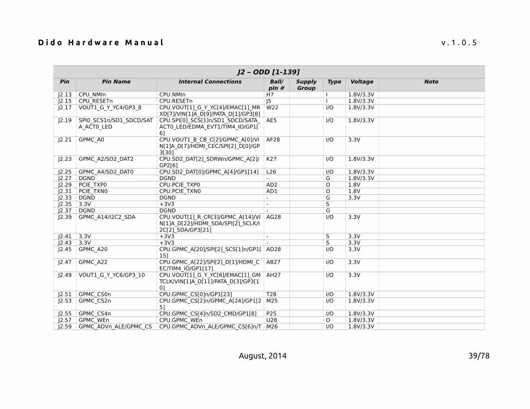
6.2 Carrier board mating connector J2J2 – ODD [1-139]
Pin Pin Name Internal Connections Ball/pin #
SupplyGroup
Type Voltage Note
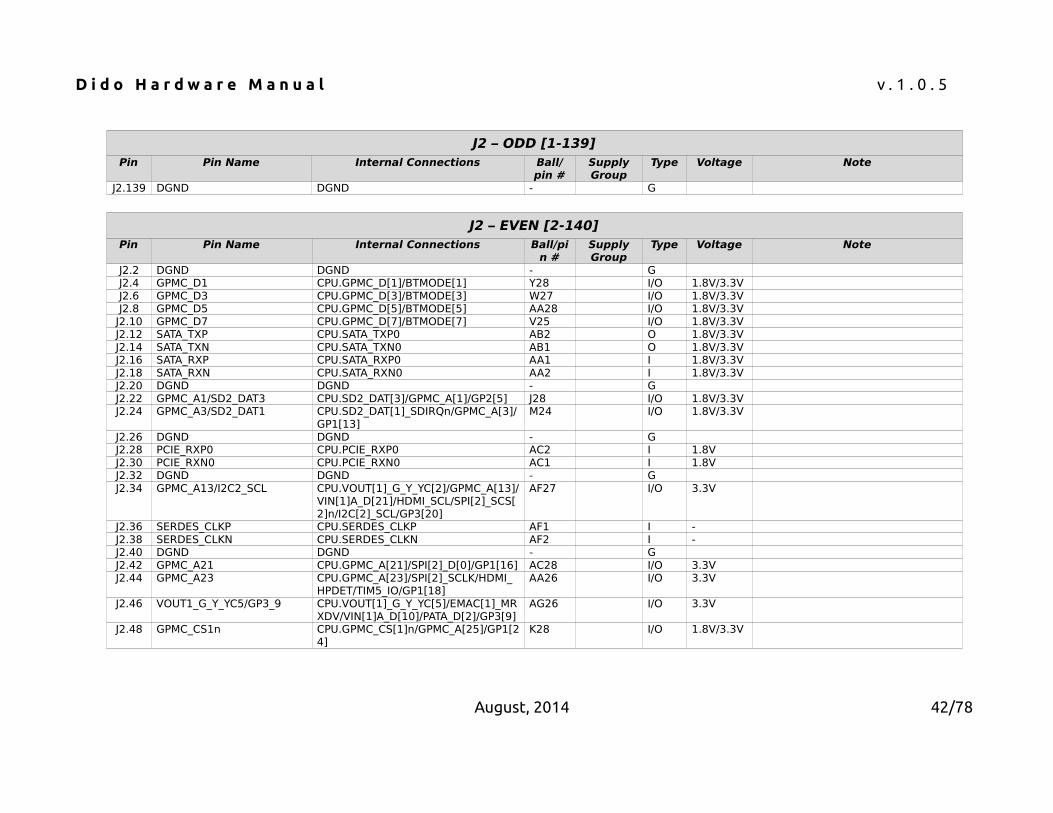
J2.1 3.3V +3V3 - SJ2.3 DGND DGND - GJ2.5 GPMC_D0 CPU.GPMC_D[0]/BTMODE[0] U26 I/O 1.8V/3.3V
J2.7 GPMC_D2 CPU.GPMC_D[2]/BTMODE[2] V27 I/O 1.8V/3.3VJ2.9 GPMC_D4 CPU.GPMC_D[4]/BTMODE[4] V26 I/O 1.8V/3.3VJ2.11 GPMC_D6 CPU.GPMC_D[6]/BTMODE[6] U25 I/O 1.8V/3.3V
August, 2014 38/78
D i d o H a r d w a r e M a n u a l v . 1 . 0 . 5
J2 – ODD [1-139]Pin Pin Name Internal Connections Ball/
pin #SupplyGroup
Type Voltage Note
J2.13 CPU_NMIn CPU.NMIn H7 I 1.8V/3.3VJ2.15 CPU_RESETn CPU.RESETn J5 I 1.8V/3.3VJ2.17 VOUT1_G_Y_YC4/GP3_8 CPU.VOUT[1]_G_Y_YC[4]/EMAC[1]_MR
XD[7]/VIN[1]A_D[9]/PATA_D[1]/GP3[8]W22 I/O 1.8V/3.3V
J2.19 SPI0_SCS1n/SD1_SDCD/SATA_ACT0_LED
CPU.SPI[0]_SCS[1]n/SD1_SDCD/SATA_ACT0_LED/EDMA_EVT1/TIM4_IO/GP1[6]
AE5 I/O 1.8V/3.3V
J2.21 GPMC_A0 CPU.VOUT1_B_CB_C[2]/GPMC_A[0]/VIN[1]A_D[7]/HDMI_CEC/SPI[2]_D[0]/GP3[30]
AF28 I/O 3.3V
J2.23 GPMC_A2/SD2_DAT2 CPU.SD2_DAT[2]_SDRWn/GPMC_A[2]/GP2[6]
K27 I/O 1.8V/3.3V
J2.25 GPMC_A4/SD2_DAT0 CPU.SD2_DAT[0]/GPMC_A[4]/GP1[14] L26 I/O 1.8V/3.3VJ2.27 DGND DGND - G 1.8V/3.3VJ2.29 PCIE_TXP0 CPU.PCIE_TXP0 AD2 O 1.8VJ2.31 PCIE_TXN0 CPU.PCIE_TXN0 AD1 O 1.8VJ2.33 DGND DGND - G 3.3VJ2.35 3.3V +3V3 - SJ2.37 DGND DGND - GJ2.39 GPMC_A14/I2C2_SDA CPU.VOUT[1]_R_CR[3]/GPMC_A[14]/VI
N[1]A_D[22]/HDMI_SDA/SPI[2]_SCLK/I2C[2]_SDA/GP3[21]
AG28 I/O 3.3V
J2.41 3.3V +3V3 - S 3.3VJ2.43 3.3V +3V3 - S 3.3VJ2.45 GPMC_A20 CPU.GPMC_A[20]/SPI[2]_SCS[1]n/GP1[
15]AD28 I/O 3.3V
J2.47 GPMC_A22 CPU.GPMC_A[22]/SPI[2]_D[1]/HDMI_CEC/TIM4_IO/GP1[17]
AB27 I/O 3.3V
J2.49 VOUT1_G_Y_YC6/GP3_10 CPU.VOUT[1]_G_Y_YC[6]/EMAC[1]_GMTCLK/VIN[1]A_D[11]/PATA_D[3]/GP3[10]
AH27 I/O 3.3V
J2.51 GPMC_CS0n CPU.GPMC_CS[0]n/GP1[23] T28 I/O 1.8V/3.3VJ2.53 GPMC_CS2n CPU.GPMC_CS[2]n/GPMC_A[24]/GP1[2
5]M25 I/O 1.8V/3.3V
J2.55 GPMC_CS4n CPU.GPMC_CS[4]n/SD2_CMD/GP1[8] P25 I/O 1.8V/3.3VJ2.57 GPMC_WEn CPU.GPMC_WEn U28 O 1.8V/3.3VJ2.59 GPMC_ADVn_ALE/GPMC_CS CPU.GPMC_ADVn_ALE/GPMC_CS[6]n/T M26 I/O 1.8V/3.3V
August, 2014 39/78
D i d o H a r d w a r e M a n u a l v . 1 . 0 . 5
J2 – ODD [1-139]Pin Pin Name Internal Connections Ball/
pin #SupplyGroup
Type Voltage Note
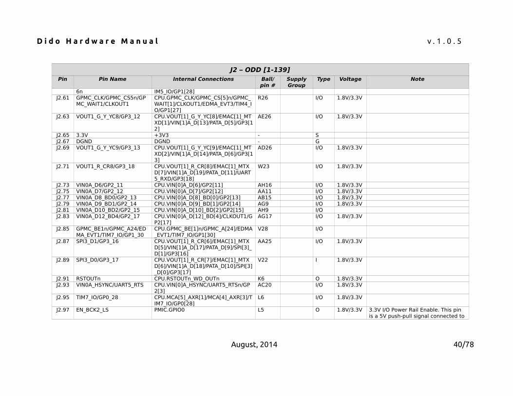
6n IM5_IO/GP1[28]J2.61 GPMC_CLK/GPMC_CS5n/GP
MC_WAIT1/CLKOUT1CPU.GPMC_CLK/GPMC_CS[5]n/GPMC_WAIT[1]/CLKOUT1/EDMA_EVT3/TIM4_IO/GP1[27]
R26 I/O 1.8V/3.3V
J2.63 VOUT1_G_Y_YC8/GP3_12 CPU.VOUT[1]_G_Y_YC[8]/EMAC[1]_MTXD[1]/VIN[1]A_D[13]/PATA_D[5]/GP3[12]
AE26 I/O 1.8V/3.3V
J2.65 3.3V +3V3 - SJ2.67 DGND DGND - GJ2.69 VOUT1_G_Y_YC9/GP3_13 CPU.VOUT[1]_G_Y_YC[9]/EMAC[1]_MT
XD[2]/VIN[1]A_D[14]/PATA_D[6]/GP3[13]
AD26 I/O 1.8V/3.3V
J2.71 VOUT1_R_CR8/GP3_18 CPU.VOUT[1]_R_CR[8]/EMAC[1]_MTXD[7]/VIN[1]A_D[19]/PATA_D[11]/UART5_RXD/GP3[18]
W23 I/O 1.8V/3.3V
J2.73 VIN0A_D6/GP2_11 CPU.VIN[0]A_D[6]/GP2[11] AH16 I/O 1.8V/3.3VJ2.75 VIN0A_D7/GP2_12 CPU.VIN[0]A_D[7]/GP2[12] AA11 I/O 1.8V/3.3VJ2.77 VIN0A_D8_BD0/GP2_13 CPU.VIN[0]A_D[8]_BD[0]/GP2[13] AB15 I/O 1.8V/3.3VJ2.79 VIN0A_D9_BD1/GP2_14 CPU.VIN[0]A_D[9]_BD[1]/GP2[14] AG9 I/O 1.8V/3.3VJ2.81 VIN0A_D10_BD2/GP2_15 CPU.VIN[0]A_D[10]_BD[2]/GP2[15] AH9 I/OJ2.83 VIN0A_D12_BD4/GP2_17 CPU.VIN[0]A_D[12]_BD[4]/CLKOUT1/G
P2[17]AG17 I/O 1.8V/3.3V
J2.85 GPMC_BE1n/GPMC_A24/EDMA_EVT1/TIM7_IO/GP1_30
CPU.GPMC_BE[1]n/GPMC_A[24]/EDMA_EVT1/TIM7_IO/GP1[30]
V28 I/O
J2.87 SPI3_D1/GP3_16 CPU.VOUT[1]_R_CR[6]/EMAC[1]_MTXD[5]/VIN[1]A_D[17]/PATA_D[9]/SPI[3]_D[1]/GP3[16]
AA25 I/O 1.8V/3.3V
J2.89 SPI3_D0/GP3_17 CPU.VOUT[1]_R_CR[7]/EMAC[1]_MTXD[6]/VIN[1]A_D[18]/PATA_D[10]/SPI[3]_D[0]/GP3[17]
V22 I 1.8V/3.3V
J2.91 RSTOUTn CPU.RSTOUTn_WD_OUTn K6 O 1.8V/3.3VJ2.93 VIN0A_HSYNC/UART5_RTS CPU.VIN[0]A_HSYNC/UART5_RTSn/GP
2[3]AC20 I/O 1.8V/3.3V
J2.95 TIM7_IO/GP0_28 CPU.MCA[5]_AXR[1]/MCA[4]_AXR[3]/TIM7_IO/GP0[28]
L6 I/O 1.8V/3.3V
J2.97 EN_BCK2_LS PMIC.GPIO0 L5 O 1.8V/3.3V 3.3V I/O Power Rail Enable. This pin is a 5V push-pull signal connected to
August, 2014 40/78
D i d o H a r d w a r e M a n u a l v . 1 . 0 . 5
J2 – ODD [1-139]Pin Pin Name Internal Connections Ball/
pin #SupplyGroup
Type Voltage Note
a voltage divider circuit via 5K6 /10K resistor, thus providing the 3V3 logical voltage output. Please refer to6.4.1.
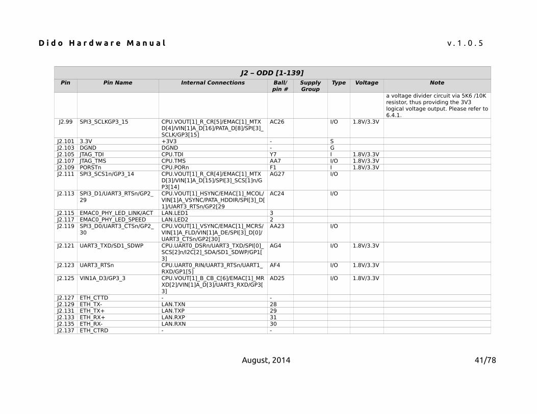
J2.99 SPI3_SCLKGP3_15 CPU.VOUT[1]_R_CR[5]/EMAC[1]_MTXD[4]/VIN[1]A_D[16]/PATA_D[8]/SPI[3]_SCLK/GP3[15]
AC26 I/O 1.8V/3.3V
J2.101 3.3V +3V3 - SJ2.103 DGND DGND - GJ2.105 JTAG_TDI CPU.TDI Y7 I 1.8V/3.3VJ2.107 JTAG_TMS CPU.TMS AA7 I/O 1.8V/3.3VJ2.109 PORSTn CPU.PORn F1 I 1.8V/3.3VJ2.111 SPI3_SCS1n/GP3_14 CPU.VOUT[1]_R_CR[4]/EMAC[1]_MTX
D[3]/VIN[1]A_D[15]/SPI[3]_SCS[1]n/GP3[14]
AG27 I/O
J2.113 SPI3_D1/UART3_RTSn/GP2_29
CPU.VOUT[1]_HSYNC/EMAC[1]_MCOL/VIN[1]A_VSYNC/PATA_HDDIR/SPI[3]_D[1]/UART3_RTSn/GP2[29
AC24 I/O
J2.115 EMAC0_PHY_LED_LINK/ACT LAN.LED1 3J2.117 EMAC0_PHY_LED_SPEED LAN.LED2 2J2.119 SPI3_D0/UART3_CTSn/GP2_
30CPU.VOUT[1]_VSYNC/EMAC[1]_MCRS/VIN[1]A_FLD/VIN[1]A_DE/SPI[3]_D[0]/UART3_CTSn/GP2[30]
AA23 I/O
J2.121 UART3_TXD/SD1_SDWP CPU.UART0_DSRn/UART3_TXD/SPI[0]_SCS[2]n/I2C[2]_SDA/SD1_SDWP/GP1[3]
AG4 I/O 1.8V/3.3V
J2.123 UART3_RTSn CPU.UART0_RIN/UART3_RTSn/UART1_RXD/GP1[5]
AF4 I/O 1.8V/3.3V
J2.125 VIN1A_D3/GP3_3 CPU.VOUT[1]_B_CB_C[6]/EMAC[1]_MRXD[2]/VIN[1]A_D[3]/UART3_RXD/GP3[3]
AD25 I/O 1.8V/3.3V
J2.127 ETH_CTTD - -J2.129 ETH_TX- LAN.TXN 28J2.131 ETH_TX+ LAN.TXP 29J2.133 ETH_RX+ LAN.RXP 31J2.135 ETH_RX- LAN.RXN 30J2.137 ETH_CTRD - -
August, 2014 41/78
D i d o H a r d w a r e M a n u a l v . 1 . 0 . 5
J2 – ODD [1-139]Pin Pin Name Internal Connections Ball/
pin #SupplyGroup
Type Voltage Note
J2.139 DGND DGND - G
J2 – EVEN [2-140]Pin Pin Name Internal Connections Ball/pi
n #SupplyGroup
Type Voltage Note
J2.2 DGND DGND - GJ2.4 GPMC_D1 CPU.GPMC_D[1]/BTMODE[1] Y28 I/O 1.8V/3.3VJ2.6 GPMC_D3 CPU.GPMC_D[3]/BTMODE[3] W27 I/O 1.8V/3.3VJ2.8 GPMC_D5 CPU.GPMC_D[5]/BTMODE[5] AA28 I/O 1.8V/3.3V
J2.10 GPMC_D7 CPU.GPMC_D[7]/BTMODE[7] V25 I/O 1.8V/3.3VJ2.12 SATA_TXP CPU.SATA_TXP0 AB2 O 1.8V/3.3VJ2.14 SATA_TXN CPU.SATA_TXN0 AB1 O 1.8V/3.3VJ2.16 SATA_RXP CPU.SATA_RXP0 AA1 I 1.8V/3.3VJ2.18 SATA_RXN CPU.SATA_RXN0 AA2 I 1.8V/3.3VJ2.20 DGND DGND - GJ2.22 GPMC_A1/SD2_DAT3 CPU.SD2_DAT[3]/GPMC_A[1]/GP2[5] J28 I/O 1.8V/3.3VJ2.24 GPMC_A3/SD2_DAT1 CPU.SD2_DAT[1]_SDIRQn/GPMC_A[3]/
GP1[13]M24 I/O 1.8V/3.3V
J2.26 DGND DGND - GJ2.28 PCIE_RXP0 CPU.PCIE_RXP0 AC2 I 1.8VJ2.30 PCIE_RXN0 CPU.PCIE_RXN0 AC1 I 1.8VJ2.32 DGND DGND - GJ2.34 GPMC_A13/I2C2_SCL CPU.VOUT[1]_G_Y_YC[2]/GPMC_A[13]/
VIN[1]A_D[21]/HDMI_SCL/SPI[2]_SCS[2]n/I2C[2]_SCL/GP3[20]
AF27 I/O 3.3V
J2.36 SERDES_CLKP CPU.SERDES_CLKP AF1 I -J2.38 SERDES_CLKN CPU.SERDES_CLKN AF2 I -J2.40 DGND DGND - GJ2.42 GPMC_A21 CPU.GPMC_A[21]/SPI[2]_D[0]/GP1[16] AC28 I/O 3.3VJ2.44 GPMC_A23 CPU.GPMC_A[23]/SPI[2]_SCLK/HDMI_
HPDET/TIM5_IO/GP1[18]AA26 I/O 3.3V
J2.46 VOUT1_G_Y_YC5/GP3_9 CPU.VOUT[1]_G_Y_YC[5]/EMAC[1]_MRXDV/VIN[1]A_D[10]/PATA_D[2]/GP3[9]
AG26 I/O 3.3V
J2.48 GPMC_CS1n CPU.GPMC_CS[1]n/GPMC_A[25]/GP1[24]
K28 I/O 1.8V/3.3V
August, 2014 42/78

D i d o H a r d w a r e M a n u a l v . 1 . 0 . 5
J2 – EVEN [2-140]Pin Pin Name Internal Connections Ball/pi
n #SupplyGroup
Type Voltage Note
J2.50 GPMC_CS3n CPU.GPMC_CS[3]n/VIN[1]B_CLK/SPI[2]_SCS[0]n/GP1[26]
P26 I/O 1.8V/3.3V
J2.52 VOUT1_G_Y_YC7/GP3_11 CPU.VOUT[1]_G_Y_YC[7]/EMAC[1]_MTXD[0]/VIN[1]A_D[12]/PATA_D[4]/GP3[11]
AF26 I/O 1.8V/3.3V
J2.54 DGND DGND - GJ2.56 GPMC_OEn_REn CPU.GPMC_OEn_REn T27 O 1.8V/3.3VJ2.58 GPMC_BE0n_CLE/GPMC_A25
/EDMA_EVT2/TIM6_IO/GP1_29
CPU.GPMC_BE[0]n_CLE/GPMC_A[25]/EDMA_EVT2/TIM6_IO/GP1[29]
U27 I/O 1.8V/3.3V
J2.60VIN[0]B_CLK/GP1[9] CPU.VIN[0]B_CLK/CLKOUT0/GP1[9] AE17 I/O 1.8V/3.3V
Module mount optionVRTC MTR - O
J2.62VOUT0_R_CR2/GP2_26 CPU.VOUT[0]_R_CR[2]/EMU4/GP2[26] AD9 I/O 1.8V/3.3V
Module mount optionPLL_1V8 MTR - O
J2.64VOUT0_R_CR3/GP2_27 CPU.VOUT[0]_R_CR[3]/GP2[27] AB9 I/O 1.8V/3.3V
Module mount optionCORE_VDD MTR - O
J2.66
VOUT1_G_Y_YC3/GP3_7GP3_23
CPU.VOUT[1]_G_Y_YC[3]/EMAC[1]_MRXD[6]/VIN[1]A_D[8]/GP3[7] (Y23)EMAC[0]_MTCLK/VIN[1]B_D[0]/SPI[3]_SCS[3]n/I2C[2]_SDA/GP3[23]
Y23L24
I/O 1.8V/3.3V
Module mount option
CVDD_ARM MTR - OJ2.68 VOUT1_R_CR9/GP3_19 CPU.VOUT[1]_R_CR[9]/EMAC[1]_MTXE
N/VIN[1]A_D[20]/PATA_D[12]/UART5_TXD/GP3[19]
Y24 I/O
J2.70 VOUT0_G_Y_YC2/GP2_24 CPU.VOUT[0]_G_Y_YC[2]/EMU3/GP2[24]
AH7 I/O 1.8V/3.3V
J2.72 VOUT0_G_Y_YC3/GP2_25 CPU.VOUT[0]_G_Y_YC[3]GP2[25] AH15 I/OJ2.74 VOUT0_B_CB_C2/GP2_22 CPU.VOUT[0]_B_CB_C[2]/EMU2/GP2[2
2]AG7 I/O 1.8V/3.3V
J2.76 VOUT0_B_CB_C3/GP2_23 CPU.VOUT[0]_B_CB_C[3]/GP2[23] AE15 I/O
J2.78MCA2_AFSX/GP0_11 CPU.MCA[2]_AFSX/GP0[11] AA5 I/O
Module mount optionCVDD_DSP MTR - O
J2.80MCA2_ACLKX/GP0_10 CPU.MCA[2]_ACLKX/GP0[10] U6 I/O 1.8V/3.3V
Module mount optionVDDQ_1V8 MTR - O
J2.82 DGND DGND - G Module mount option
August, 2014 43/78
D i d o H a r d w a r e M a n u a l v . 1 . 0 . 5
J2 – EVEN [2-140]Pin Pin Name Internal Connections Ball/pi
n #SupplyGroup
Type Voltage Note
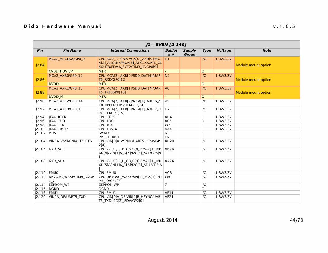
J2.84
MCA2_AHCLKX/GP0_9 CPU.AUD_CLKIN2/MCA[0]_AXR[9]/MCA[2]_AHCLKX/MCA[5]_AHCLKX/ATL_CLKOUT3/EDMA_EVT2/TIM3_IO/GP0[9]
H1 I/O 1.8V/3.3V
Module mount option
CVDD_HDVICP MTR - O
J2.86MCA2_AXR0/GP0_12 CPU.MCA[2]_AXR[0]/SD0_DAT[6]/UAR
T5_RXD/GP0[12]N2 I/O 1.8V/3.3V
Module mount optionDVDD MTR - O
J2.88MCA2_AXR1/GP0_13 CPU.MCA[2]_AXR[1]/SD0_DAT[7]/UAR
T5_TXD/GP0[13]V6 I/O 1.8V/3.3V
Module mount optionDVDD_M MTR - O
J2.90 MCA2_AXR2/GP0_14 CPU.MCA[2]_AXR[2]/MCA[1]_AXR[6]/SC0_VPPEN/TIM2_IO/GP0[14]
V5 I/O 1.8V/3.3V
J2.92 MCA2_AXR3/GP0_15 CPU.MCA[2]_AXR[3]/MCA[1]_AXR[7]/TIM3_IO/GP0[15]
H2 I/O 1.8V/3.3V
J2.94 JTAG_RTCK CPU.RTCK AD4 I 1.8V/3.3VJ2.96 JTAG_TDO CPU.TDO AC5 O 1.8V/3.3VJ2.98 JTAG_TCK CPU.TCK W7 I 1.8V/3.3VJ2.100 JTAG_TRSTn CPU.TRSTn AA4 I 1.8V/3.3VJ2.102 MRST SV.MR
PMIC.HDRST6L6
II
J2.104 VIN0A_VSYNC/UART5_CTS CPU.VIN[0]A_VSYNC/UART5_CTSn/GP2[4]
AD20 I/O 1.8V/3.3V
J2.106 I2C3_SCL CPU.VOUT[1]_B_CB_C[8]/EMAC[1]_MRXD[4]/VIN[1]A_D[5]/I2C[3]_SCL/GP3[5]
AH26 I/O 1.8V/3.3V
J2.108 I2C3_SDA CPU.VOUT[1]_B_CB_C[9]/EMAC[1]_MRXD[5]/VIN[1]A_D[6]/I2C[3]_SDA/GP3[6]
AA24 I/O 1.8V/3.3V
J2.110 EMU0 CPU.EMU0 AG8 I/O 1.8V/3.3VJ2.112 DEVOSC_WAKE/TIM5_IO/GP
1_7CPU.DEVOSC_WAKE/SPI[1]_SCS[1]n/TIM5_IO/GP1[7]
W6 I/O 1.8V/3.3V
J2.114 EEPROM_WP EEPROM.WP 7 I/OJ2.116 DGND DGND - GJ2.118 EMU1 CPU.EMU1 AE11 I/O 1.8V/3.3VJ2.120 VIN0A_DE/UART5_TXD CPU.VIN[0]A_DE/VIN[0]B_HSYNC/UAR
T5_TXD/I2C[2]_SDA/GP2[0]AE21 I/O 1.8V/3.3V
August, 2014 44/78
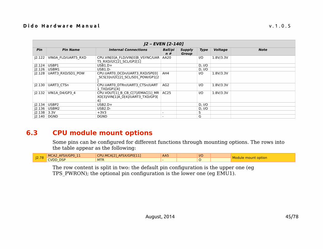
D i d o H a r d w a r e M a n u a l v . 1 . 0 . 5
J2 – EVEN [2-140]Pin Pin Name Internal Connections Ball/pi
n #SupplyGroup
Type Voltage Note
J2.122 VIN0A_FLD/UART5_RXD CPU.VIN[0]A_FLD/VIN[0]B_VSYNC/UART5_RXD/I2C[2]_SCL/GP2[1]
AA20 I/O 1.8V/3.3V
J2.124 USBP1 USB1.D+ D, I/OJ2.126 USBM1 USB1.D- D, I/OJ2.128 UART3_RXD/SD1_POW CPU.UART0_DCDn/UART3_RXD/SPI[0]
_SCS[3]n/I2C[2]_SCL/SD1_POW/GP1[2]
AH4 I/O 1.8V/3.3V
J2.130 UART3_CTSn CPU.UART0_DTRn/UART3_CTSn/UART1_TXD/GP1[4]
AG2 I/O 1.8V/3.3V
J2.132 VIN1A_D4/GP3_4 CPU.VOUT[1]_B_CB_C[7]/EMAC[1]_MRXD[3]/VIN[1]A_D[4]/UART3_TXD/GP3[4]
AC25 I/O 1.8V/3.3V
J2.134 USBP2 USB2.D+ D, I/OJ2.136 USBM2 USB2.D- D, I/OJ2.138 3.3V +3V3 - SJ2.140 DGND DGND - G
6.3 CPU module mount optionsSome pins can be configured for different functions through mounting options. The rows intothe table appear as the following:
J2.78MCA2_AFSX/GP0_11 CPU.MCA[2]_AFSX/GP0[11] AA5 I/O
Module mount optionCVDD_DSP MTR - O
The row content is split in two: the default pin configuration is the upper one (eg TPS_PWRON); the optional pin configuration is the lower one (eg EMU1).
August, 2014 45/78
D i d o H a r d w a r e M a n u a l v . 1 . 0 . 5
6.4 Additional notes
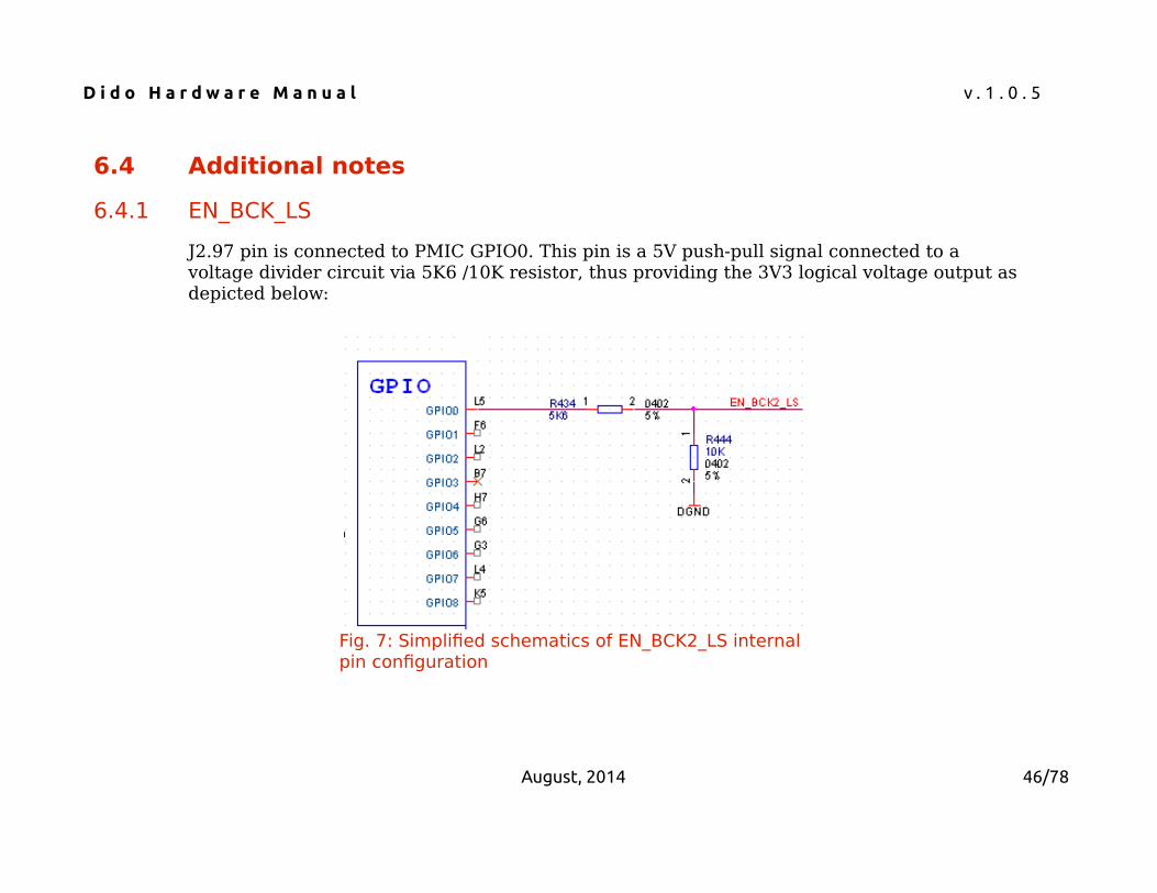
6.4.1 EN_BCK_LS
J2.97 pin is connected to PMIC GPIO0. This pin is a 5V push-pull signal connected to a voltage divider circuit via 5K6 /10K resistor, thus providing the 3V3 logical voltage output asdepicted below:
August, 2014 46/78
Fig. 7: Simplified schematics of EN_BCK2_LS internal pin configuration
D i d o H a r d w a r e M a n u a l v . 1 . 0 . 5
7 Peripheral interfacesDIDO modules implement a number of peripheral interfaces through the J1 and J2 connectors. The following notes apply to those interfaces: Some interfaces/signals are available only with/without
certain configuration options of the DIDO module. Each signal’s availability is noted in the “Notes” column on the table of each interface.
The signals for each interface are described in the related tables. The following notes summarize the column headers for these tables: “Pin name” – The symbolic name of each signal
“Conn. Pin” – The pin number on the module connectors
“Function” – Signal description
“Notes” – This column summarizes configuration requirements and recommendations for each signal.
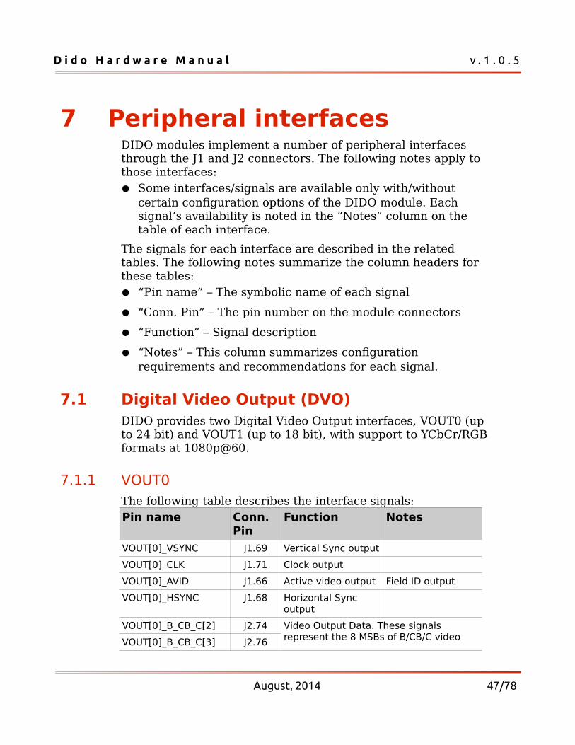
7.1 Digital Video Output (DVO)DIDO provides two Digital Video Output interfaces, VOUT0 (up to 24 bit) and VOUT1 (up to 18 bit), with support to YCbCr/RGBformats at 1080p@60.
7.1.1 VOUT0The following table describes the interface signals:Pin name Conn.
PinFunction Notes
VOUT[0]_VSYNC J1.69 Vertical Sync output
VOUT[0]_CLK J1.71 Clock output
VOUT[0]_AVID J1.66 Active video output Field ID output
VOUT[0]_HSYNC J1.68 Horizontal Sync output
VOUT[0]_B_CB_C[2] J2.74 Video Output Data. These signals represent the 8 MSBs of B/CB/C video VOUT[0]_B_CB_C[3] J2.76
August, 2014 47/78
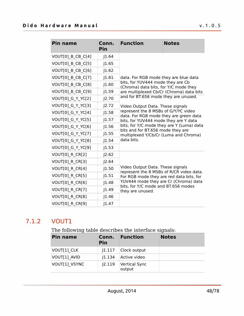
D i d o H a r d w a r e M a n u a l v . 1 . 0 . 5
Pin name Conn. Pin
Function Notes
data. For RGB mode they are blue data bits, for YUV444 mode they are Cb (Chroma) data bits, for Y/C mode they are multiplexed Cb/Cr (Chroma) data bitsand for BT.656 mode they are unused.
VOUT[0]_B_CB_C[4] J1.64
VOUT[0]_B_CB_C[5] J1.65
VOUT[0]_B_CB_C[6] J1.62
VOUT[0]_B_CB_C[7] J1.61
VOUT[0]_B_CB_C[8] J1.60
VOUT[0]_B_CB_C[9] J1.59
VOUT[0]_G_Y_YC[2] J2.70
Video Output Data. These signals represent the 8 MSBs of G/Y/YC video data. For RGB mode they are green data bits, for YUV444 mode they are Y data bits, for Y/C mode they are Y (Luma) databits and for BT.656 mode they are multiplexed Y/Cb/Cr (Luma and Chroma) data bits.
VOUT[0]_G_Y_YC[3] J2.72
VOUT[0]_G_Y_YC[4] J1.58
VOUT[0]_G_Y_YC[5] J1.57
VOUT[0]_G_Y_YC[6] J1.56
VOUT[0]_G_Y_YC[7] J1.55
VOUT[0]_G_Y_YC[8] J1.54
VOUT[0]_G_Y_YC[9] J1.53
VOUT[0]_R_CR[2] J2.62
Video Output Data. These signals represent the 8 MSBs of R/CR video data.For RGB mode they are red data bits, for YUV444 mode they are Cr (Chroma) databits, for Y/C mode and BT.656 modes they are unused.
VOUT[0]_R_CR[3] J2.64
VOUT[0]_R_CR[4] J1.50
VOUT[0]_R_CR[5] J1.51
VOUT[0]_R_CR[6] J1.48
VOUT[0]_R_CR[7] J1.49
VOUT[0]_R_CR[8] J1.46
VOUT[0]_R_CR[9] J1.47
7.1.2 VOUT1The following table describes the interface signals:Pin name Conn.
PinFunction Notes
VOUT[1]_CLK J1.117 Clock output
VOUT[1]_AVID J1.134 Active video
VOUT[1]_VSYNC J2.119 Vertical Sync output
August, 2014 48/78

D i d o H a r d w a r e M a n u a l v . 1 . 0 . 5
Pin name Conn. Pin
Function Notes
VOUT[1]_HSYNC J2.113 Horizontal Sync output
VOUT[1]_B_CB_C[4] J1.11Video Output Data. These signals represent the 6 MSBs of B/CB/C video data. For RGB mode they are blue data bits, for YUV444 mode they are Cb (Chroma) data bits, for Y/C mode they are multiplexed Cb/Cr (Luma) data bits, and for BT.656 mode they are not used.
VOUT[1]_B_CB_C[5] J1.14
VOUT[1]_B_CB_C[6] J2.125
VOUT[1]_B_CB_C[7] J2.132
VOUT[1]_B_CB_C[8] J2.106
VOUT[1]_B_CB_C[9] J2.108
VOUT[1]_G_Y_YC[4] J2.17 Video Output Data. These signals represent the 6 MSBs of G/Y/YC video data. For RGB mode they are green data bits, for YUV444 mode they are Y data bits, for Y/C mode they are Y (Luma) databits and for BT.656 mode they are multiplexed Y/Cb/Cr (Luma and Chroma) data bits.
VOUT[1]_G_Y_YC[5] J2.46
VOUT[1]_G_Y_YC[6] J2.49
VOUT[1]_G_Y_YC[7] J2.52
VOUT[1]_G_Y_YC[8] J2.63
VOUT[1]_G_Y_YC[9] J2.69
VOUT[1]_R_CR[4] J2.111Video Output Data. These signals represent the 6 MSBs of R/CR video data.For RGB mode they are red data bits, for YUV444 mode they are Cr (Chroma) databits, for Y/C mode and BT.656 mode theyare not used.
VOUT[1]_R_CR[5] J2.99
VOUT[1]_R_CR[6] J2.87
VOUT[1]_R_CR[7] J2.89
VOUT[1]_R_CR[8] J2.71
VOUT[1]_R_CR[9] J2.68
7.2 HDMIDIDO includes an High Definition Multimedia Interface 1.3a compliant transmitter for digital audio and video, with integrated HDCP (High-bandwidth Digital Content Protection) and 1080p60 support. The HDMI interface consists of a digital HDMI transmitter core with TMDS encoder, a core wrapper with interface logic and control registers, and a transmit PHY. HDMI shares the digital video chain with the VOUT1 port, so when both interfaces are enabled, the same content is reproduced.The following table describes the interface signals:
August, 2014 49/78
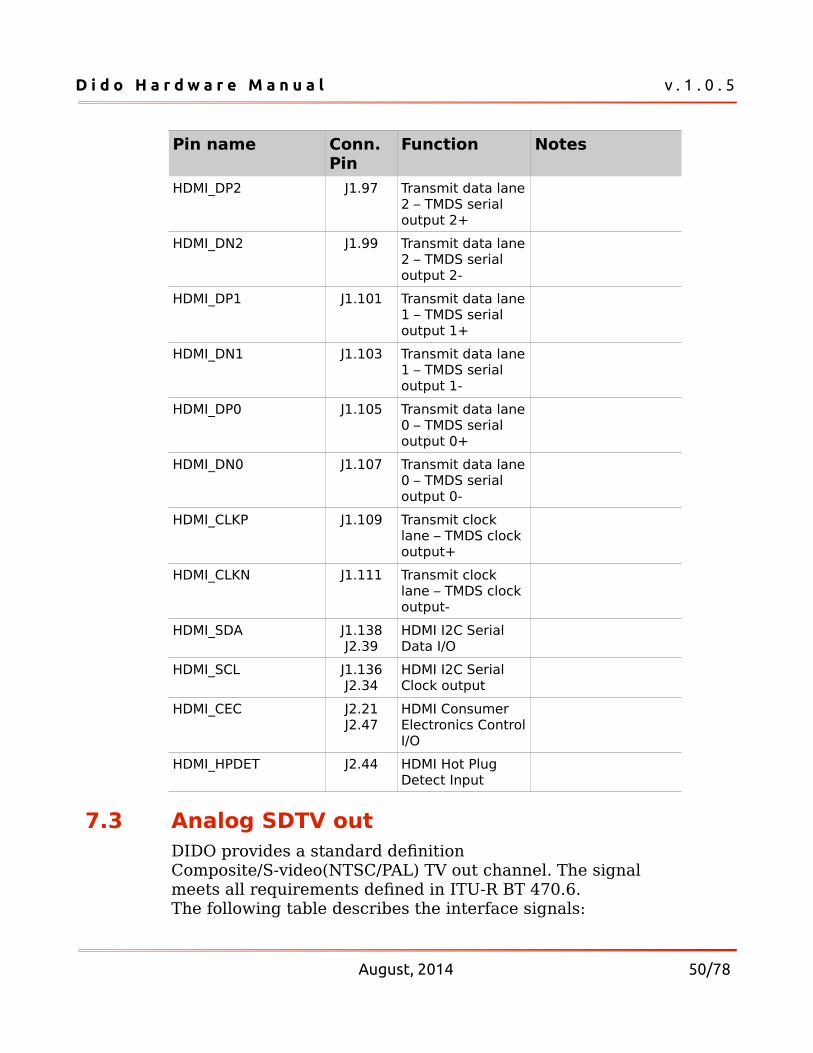
D i d o H a r d w a r e M a n u a l v . 1 . 0 . 5
Pin name Conn. Pin
Function Notes
HDMI_DP2 J1.97 Transmit data lane2 – TMDS serial output 2+
HDMI_DN2 J1.99 Transmit data lane2 – TMDS serial output 2-
HDMI_DP1 J1.101 Transmit data lane1 – TMDS serial output 1+
HDMI_DN1 J1.103 Transmit data lane1 – TMDS serial output 1-
HDMI_DP0 J1.105 Transmit data lane0 – TMDS serial output 0+
HDMI_DN0 J1.107 Transmit data lane0 – TMDS serial output 0-
HDMI_CLKP J1.109 Transmit clock lane – TMDS clock output+
HDMI_CLKN J1.111 Transmit clock lane – TMDS clock output-
HDMI_SDA J1.138J2.39
HDMI I2C Serial Data I/O
HDMI_SCL J1.136J2.34
HDMI I2C Serial Clock output
HDMI_CEC J2.21J2.47
HDMI Consumer Electronics ControlI/O
HDMI_HPDET J2.44 HDMI Hot Plug Detect Input
7.3 Analog SDTV outDIDO provides a standard definition Composite/S-video(NTSC/PAL) TV out channel. The signal meets all requirements defined in ITU-R BT 470.6.The following table describes the interface signals:
August, 2014 50/78
D i d o H a r d w a r e M a n u a l v . 1 . 0 . 5
Pin name Conn. Pin
Function Notes
TV_OUT1 J1.131 Composite/S-Video(Luminance) Amplifier Output
Configured as “Normal mode” (internal amplifier used). This pin drivesthe 75- TVΩload.
TV_OUT2 J1.133 S-Video (Chrominance) Amplifier Output
Configured as “Normal mode” (internal amplifier used). This pin drivesthe 75- TVΩload.
7.4 Digital Video Input portsThe HD Video Processing Subsystem supports two independently configurable external video input capture ports (VIP) up to 165MHz. Each video capture port supports one scaler capable of both up and down scaling of one non-multiplexed input stream; each video capture port supportsone programmable color space conversion to convert between 24-bit RGB data and YCbCr data. The VIP supports data storage in RGB, 422, and 420 formats and each video capture port channel supports chroma down-sampling (422 to 420) for any non-multiplexed input data. The chroma down-sampling formultiplexed streams is done as memory to memory operations outside of HDVPSS on an individual frame data. Two VIP instances are not identical from chip level. VIP instance 0 is a 24-bit interface and VIP instance 1 is a 16-bit interface. The HDVPSS supports two independent pixel clock input domains for each VIP, called Port A and Port B. Port A supports a single up to 24 bit data bus at the instance level and Port B supports asingle 8 bit data bus at the instance level. The configuration foreach device input port is described in the following table:
Port A Port B
8 bit Off
16 bit Off
24 bit Off
8 bit 8 bit
August, 2014 51/78
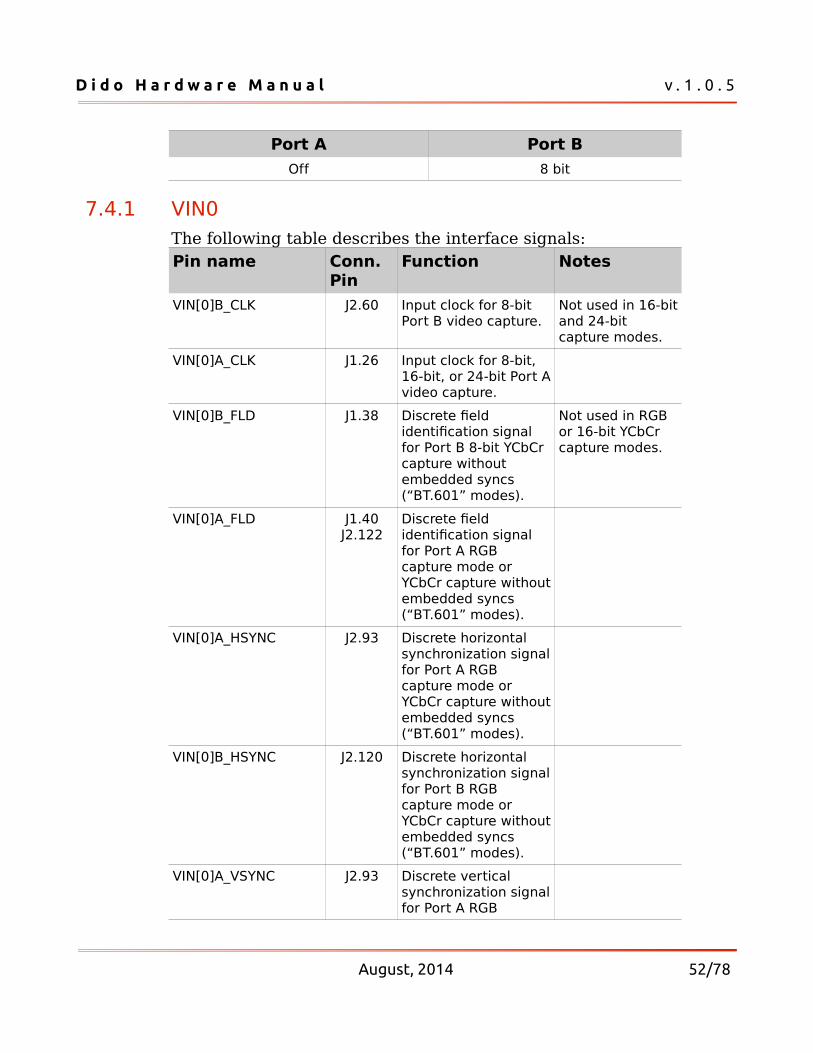
D i d o H a r d w a r e M a n u a l v . 1 . 0 . 5
Port A Port B
Off 8 bit
7.4.1 VIN0The following table describes the interface signals:Pin name Conn.
PinFunction Notes
VIN[0]B_CLK J2.60 Input clock for 8-bit Port B video capture.
Not used in 16-bitand 24-bit capture modes.
VIN[0]A_CLK J1.26 Input clock for 8-bit, 16-bit, or 24-bit Port Avideo capture.
VIN[0]B_FLD J1.38 Discrete field identification signal for Port B 8-bit YCbCr capture without embedded syncs (“BT.601” modes).
Not used in RGB or 16-bit YCbCr capture modes.
VIN[0]A_FLD J1.40J2.122
Discrete field identification signal for Port A RGB capture mode or YCbCr capture withoutembedded syncs (“BT.601” modes).
VIN[0]A_HSYNC J2.93 Discrete horizontal synchronization signalfor Port A RGB capture mode or YCbCr capture withoutembedded syncs (“BT.601” modes).
VIN[0]B_HSYNC J2.120 Discrete horizontal synchronization signalfor Port B RGB capture mode or YCbCr capture withoutembedded syncs (“BT.601” modes).
VIN[0]A_VSYNC J2.93 Discrete vertical synchronization signalfor Port A RGB
August, 2014 52/78
D i d o H a r d w a r e M a n u a l v . 1 . 0 . 5
Pin name Conn. Pin
Function Notes
capture mode or YCbCr capture withoutembedded syncs (“BT.601” modes).
VIN[0]B_VSYNC J2.122 Discrete vertical synchronization signalfor Port B RGB capture mode or YCbCr capture withoutembedded syncs (“BT.601” modes).
VIN[0]B_DE J1.42 Discrete data valid signal for Port B RGB capture mode or capture without embedded syncs (“BT.601” modes).
VIN[0]A_DE J1.44J2.120
Discrete data valid signal for Port A RGB capture mode or YcbCr capture withoutembedded syncs ("BT.601" modes).
VIN[0]A_D[0] J1.30 Data inputs. For 16-bit capture, D[7:0] are Cb/Cr and [15:8] are Y Port A inputs. For 8-bit capture, D[7:0] are Port A YCbCrdata inputs and D[15:8] are Port B YCbCrdata inputs. For RGB capture, D[23:16] are R, D[15:8] are G, and BD[7:0] are B data inputs.
VIN[0]A_D[1] J1.32
VIN[0]A_D[2] J1.36
VIN[0]A_D[3] J1.116
VIN[0]A_D[4] J1.120
VIN[0]A_D[5] J1.122
VIN[0]A_D[6] J2.73
VIN[0]A_D[7] J2.75
VIN[0]A_D[8]_BD[0] J2.77
VIN[0]A_D[9]_BD[1] J2.79
VIN[0]A_D[10]_BD[2] J2.81
VIN[0]A_D[11]_BD[3] J1.22
VIN[0]A_D[12]_BD[4] J2.83
VIN[0]A_D[13]_BD[5] J1.18
August, 2014 53/78
D i d o H a r d w a r e M a n u a l v . 1 . 0 . 5
Pin name Conn. Pin
Function Notes
VIN[0]A_D[14]_BD[6] J1.20
VIN[0]A_D[15]_BD[7] J1.24
VIN[0]A_D[16] J1.23
VIN[0]A_D[17] J1.25
VIN[0]A_D[18] J1.27
VIN[0]A_D[19] J1.29
VIN[0]A_D[20] J1.31
VIN[0]A_D[21] J1.33
VIN[0]A_D[22] J1.92
VIN[0]A_D[23] J1.94
7.4.2 VIN1The following table describes the interface signals:Pin name Conn.
PinFunction Notes
VIN[1]A_CLK J1.134 Input clock for 8-bit, 16-bit, or 24-bit Port A video capture.
Input data is sampled on the CLK0 edge.
VIN[1]A_VSYNC J2.113 Discrete vertical synchronization signal for Port A YCbCr capture modes without embedded syncs (“BT.601” modes).
VIN[1]A_HSYNK J1.117 Discrete horizontal synchronization signal forPort A YCbCr capture modes without embedded syncs (“BT.601” modes).
VIN[1]A_DE J2.119 Discrete data valid signal for Port A RGB capture mode
August, 2014 54/78
D i d o H a r d w a r e M a n u a l v . 1 . 0 . 5
Pin name Conn. Pin
Function Notes
or YcbCr capture without embedded syncs ("BT.601" modes).
VIN[1]A_FLD J2.119 Discrete field identification signal for Port A YCbCr capture modes without embedded syncs (“BT.601” modes).
VIN[1]A_D[0] J1.132 Video Input 1 Data inputs. For 16-bit capture, D[7:0] are Cb/Cr and [15:8] are Y Port A inputs. For 8-bit capture, are Port A YCbCr data inputs. For RGB capture, D[23:16] are R, D[15:8] are G, and D[7:0] are B Port A data inputs.
VIN[1]A_D[1] J1.11
VIN[1]A_D[2] J1.14
VIN[1]A_D[3] J2.125
VIN[1]A_D[4] J2.132
VIN[1]A_D[5] J2.106
VIN[1]A_D[6] J2.108
VIN[1]A_D[7] J2.21
Please note that, in order to use this port
I2C3 bus must be disabled. As a consequence keypad controller, EEPROM and touch screen controller are not available.
Gigabit Ethernet must be disabled. As a consequence only FastEthernet Interface is available and Ethernet Switch is working with only one port.
HDMI CEC must be disabled. Please note that CEC is optional on HDMI interface and is currently used only in consumer devices.
7.5 Ethernet portsThe DM814x/AM387x 3PSW (Three Port Switch) Ethernet Subsystem provides ethernet packet communication and can beconfigured as an ethernet switch. It provides the gigabit media
August, 2014 55/78
D i d o H a r d w a r e M a n u a l v . 1 . 0 . 5
independent interface (G/MII), reduced gigabit media independent interface (RGMII), reduced media independent interface (RMII), the management data input output (MDIO) forphysical layer device (PHY) management. DIDO provides two ethernet ports, one Fast Ethernet with on-board PHY, and one Gigabit Ethernet (GRMII only).
7.5.1 EMAC_RMREFCLKEMAC_REFCLK signal is the reference clock for the internal PHY (SMSC LAN8710) connected to EMAC[0] configured in RMII mode. This signal is driven by the CPU and can be optionally routed to J1.91 through a mount option. The CPU.EMAC_RMREFCLK signal is internally split in two lines, one connected to the internal PHY and the other routed to the J1 connector; both lines are terminated with 22 Ω resistors. Formore flexibility on using both EMAC[0] and EMAC[1] interfaces, this signal has been routed to the J1 connector providing the following configuration options: generated internally (default configuration) and routed
externally for driving an external RMII PHY on the second MAC (EMAC[1]) at 10/100 Mbit. In this case it is possible to avoid the cost of an external crystal or oscillator.
generated by an external PHY mounted on the carrier board (connected to EMAC[1]) and routed internally to the internal PHY and CPU. In some cases this configuration could be preferred.
7.5.2 Ethernet 10/100On-board Ethernet PHY provides interface signals required to implement the 10/100 Ethernet port. It is connected to processor EMAC0 controller through RMII interface.The following table describes the interface signals:Pin name Conn.
PinFunction Notes
EMAC0_PHY_LED_LINK/ACT
J2.115 Link activity LED Indication.
This pin is driven active when a valid link is detected and blinks when activity is detected.
August, 2014 56/78

D i d o H a r d w a r e M a n u a l v . 1 . 0 . 5
Pin name Conn.Pin
Function Notes
EMAC0_PHY_LED_SPEED J2.117 Link Speed LED Indication.
This pin is driven active when the operating speed is 100Mbps. It is inactive when the operating speed is 10Mbps or during line isolation.
ETH_CTTD J2.127 Tx Center Tap
ETH_CTRD J2.137 Rx Center Tap
ETH_TX- J2.129 Transmit NegativeChannel
ETH_TX+ J2.131 Transmit Positive Channel
ETH_RX- J2.135 Receive Negative Channel
ETH_RX+ J2.133 Receive Positive Channel
EMAC_RMREFCLK J1.91 RMII Reference Clock
7.5.3 Gigabit EMACDIDO provides a Gigabit Ethernet interface connected to processor EMAC1 controller through GRMII interface. When required, an external PHY must be mounted on the carrier board.The following table describes the interface signals:Pin name Conn.
PinFunction Notes
EMAC[1]_RGRXC J1.78 RGMII Receive Clock
EMAC[1]_RGRXCTL J1.108 RGMII Receive Control
EMAC[1]_RGRXD[3] J1.80 RGMII Receive Data [3:0]
EMAC[1]_RGRXD[2] J1.86
EMAC[1]_RGRXD[1] J1.88
August, 2014 57/78
D i d o H a r d w a r e M a n u a l v . 1 . 0 . 5
Pin name Conn.Pin
Function Notes
EMAC[1]_RGRXD[0] J1.106
EMAC[1]_RGTXC J1.87 RGMII Transmit Clock
EMAC[1]_RGTXCTL J1.110 RGMII Transmit Enable
EMAC[1]_RGTXD[3] J1.112 RGMII Transmit Data [3:0]
EMAC[1]_RGTXD[2] J1.77
EMAC[1]_RGTXD[1] J1.79
EMAC[1]_RGTXD[0] J1.85
EMAC_RMREFCLK J1.91 RMII Reference Clock
7.6 CAN portsDIDO provides two DCAN interfaces (DCAN0 and DCAN1) for supporting distributed realtime control with a high level of security. The DCAN interfaces implement the CAN protocol version 2.0 part A, B and supports bit rates up to 1 Mbit/s.
7.6.1 DCAN0DCAN0 port is connected to on-board transceiver which converts the single-ended CAN signals of the controller to the differential signals of the physical layer. The following table describes the interface signals:Pin name Conn.
PinFunction Notes
CAN_H J1.96 High bus output
CAN_L J1.98 Low bus output
7.6.2 DCAN1When required, DCAN1 must be connected to an external PHY.The following table describes the interface signals:
August, 2014 58/78
D i d o H a r d w a r e M a n u a l v . 1 . 0 . 5
Pin name Conn.Pin
Function Notes
DCAN1_RX J1.19 Receive data pin
DCAN1_TX J1.21 Transmit data pin
7.7 UARTsThree UART ports are routed to DIDO connectors. UART0 provides full Modem Control Signals, while UART3 and UART5 are 4-wire interfaces. Each port can be programmed separatelyand can operate in UART, IrDA or CIR modes.
7.7.1 UART0The following table describes the interface signals:Pin name Conn.
PinFunction Note
UART0_RXD J1.7 Receive Data Functions as IrDA receive input in IrDA modes and CIR receive input in CIR mode
UART0_TXD J1.8 Transmit Data Functions as CIR transmit in CIR mode
UART0_RTSn J1.19 Request To Send Functions as transmitdata output in IrDA modes
UART0_CTSn J1.21 Clear To Send Functions as SD transceiver control output in IrDA and CIR modes
UART0_DTRn J2.130 Data Terminal Ready
UART0_DSRn J2.121 Data Set Ready
UART0_DCDn J2.128 Data Carrier Detect
UART0_RIN J2.123 Ring indicator
August, 2014 59/78
D i d o H a r d w a r e M a n u a l v . 1 . 0 . 5
7.7.2 UART3The following table describes the interface signals:Pin name Conn.
PinFunction Notes
UART3_RXD J2.128 Receive Data Also available as alternative function on pin J2.125. Functions as IrDA receive input in IrDA modes and CIR receive input in CIR mode.
UART3_TXD J2.121 Transmit Data Also available as alternative function on pin J2.132. Functions as CIR transmit in CIR mode.
UART3_RTSn J2.123 Request To Send Also available as alternative function on pin J1.113. Functions as transmitdata output in IrDA modes
UART3_CTSn J2.130 Clear To Send Also available as alternative function on pin J1.119. Functions as SD transceiver control output in IrDA and CIR modes.
7.7.3 UART5The following table describes the interface signals:Pin name Conn.
PinFunction Notes
UART5_RXD J2.122 Receive Data Also available as alternative function on pin J2.86. Functions as IrDA receive input in IrDA
August, 2014 60/78
D i d o H a r d w a r e M a n u a l v . 1 . 0 . 5
Pin name Conn.Pin
Function Notes
modes and CIR receive input in CIR mode.
UART5_TXD J2.120 Transmit Data Also available as alternative function on pin J2.88. Functions as CIR transmit in CIR mode.
UART5_RTSn J1.93 Request To Send Functions as transmitdata output in IrDA modes
UART5_CTSn J2.104 Clear To Send Functions as SD transceiver control output in IrDA and CIR modes.
7.8 MMC/SD channelsThree standard MMC/SD/SDIO interfaces are available on DIDO module. The processor includes 3 MMC/SD/SDIO Controllers which are compliant with MMC V4.3, Secure Digital Part 1 Physical Layer Specification V2.00 and Secure Digital Input Output (SDIO) V2.00 specifications. High capacitySD cards (SDHC) are supported.
7.8.1 MMC/SD/SDIO0MMC/SD0 can be configured as 1-bit or 4-bit mode. When using this channel, MMC/SD0 can't be configured as 8-bit mode.The following table describes the interface signals:Pin name Conn.
PinFunction Notes
SD0_CLK J1.124 Clock output
SD0_CMD J1.130 Command output
SD0_DAT[0] J1.127 Data bit 0 Functions as single data bit for 1-bit SD mode.
August, 2014 61/78

D i d o H a r d w a r e M a n u a l v . 1 . 0 . 5
Pin name Conn.Pin
Function Notes
SD0_DAT[1] J1.129 Data bit 1 Functions as an IRQ input for 1-bit SD mode.
SD0_DAT[2] J1.102 Data bit 2 Functions as a Read Wait input for 1-bit SD mode.
SD0_DAT[3] J1.104 Data bit 3
7.8.2 MMC/SD/SDIO1MMC/SD1 can be configured as 1-bit, 4-bit or 8-bit mode. Please note that 8-bit mode can be used only when MMC/SD0 is not enabled.The following table describes the interface signals:Pin name Conn.
PinFunction Notes
SD1_CLK J1.137 Clock output
SD1_CMD J1.135 Command output Also available as alternative function on pin J1.130.
SD1_DAT[0] J1.119 Data bit 0 Functions as single data bit for 1-bit SD mode.
SD1_DAT[1] J1.121 Data bit 1 Functions as an IRQ input for 1-bit SD mode.
SD1_DAT[2] J1.123 Data bit 2 Functions as a Read Wait input for 1-bit SD mode.
SD1_DAT[3] J1.125 Data bit 3
SD1_DAT[4] J1.127 Data bit 4
SD1_DAT[5] J1.129 Data bit 5
SD1_DAT[6] J1.102 Data bit 6
SD1_DAT[7] J1.104 Data bit 7
August, 2014 62/78

D i d o H a r d w a r e M a n u a l v . 1 . 0 . 5
7.8.3 MMC/SD/SDIO2The following table describes the interface signals:Pin name Conn.
PinFunction Notes
SD2_SCLK J1.128 Clock output
SD2_CMD J2.55 Command output
SD2_DAT[0] J2.25 Data bit 0 Functions as single data bit for 1-bit SD mode.
SD2_DAT[1] J2.24 Data bit 1 Functions as an IRQ input for 1-bit SD mode.
SD2_DAT[2] J2.23 Data bit 2 Functions as a Read Wait input for 1-bit SD mode.
SD2_DAT[3] J2.22 Data bit 3
7.9 USB portsDIDO provides three USB 2.0 ports with integrated PHY. USB0 is a OTG 2.0 port, USB1 is a Host/OTG 2.0 port and USB2 is a 2.0 Host port. USB1 can be configured through dedicated mount options. USB1 and USB2 are the downstreams of a USB hub connected to the second USB controller provided by the processor.
7.9.1 USB0The following table describes the interface signals:Pin name Conn.
PinFunction Notes
USB0_DP J1.6 Bidirectional data differential signal pair (plus/minus)
USB0_DM J1.5
USB0_ID J1.17 OTG identificationinput.
USB0_VBUSIN J1.16 5-V VBUS comparator input.
Senses the level of the USB VBUS. Should connect directly to the USB VBUS voltage.
August, 2014 63/78
D i d o H a r d w a r e M a n u a l v . 1 . 0 . 5
Pin name Conn.Pin
Function Notes
USB0_DRVVBUS J1.93 Used by the USB0Controller to enable the external VBUS charge pump.
7.9.2 USB1The following table describes the interface signals:Pin name Conn.
PinFunction Notes
USBP1 J2.124 Bidirectional data differential signal pair (plus/minus)
USBM1 J2.126
7.9.3 USB2The following table describes the interface signals:Pin name Conn.
PinFunction Notes
USBP2 J2.134 Bidirectional data differential signal pair (plus/minus)
USBM2 J2.136
7.9.4 Other USB signalsThe following table describes the interface signals:Pin name Conn.
PinFunction Notes
USB1_VBUS J1.95 5-V VBUS comparator input.
Senses the level of the USB VBUS. Should connect directly to the USB VBUS voltage.
USB1_DRVVBUS J1.118 Used by the USB1 Controller to enable the external VBUS charge pump.
August, 2014 64/78
D i d o H a r d w a r e M a n u a l v . 1 . 0 . 5
7.10 TouchscreenThe touch screen controller is a TSC2003 resistive 4-wire controller connected to the I2C-3 bus. It also provides an auxiliary 12-bit A/D converter channel.Device address is 1001000b.The following table describes the interface signals:Connector Pin Pin
nameFunction Notes
TSC_XP J1.39 X+ Position Input Please considerthe use of ESD
protectiondevices on carrierboard when these
pins areconnected toactual touch
screen.
TSC_XM J1.41 X- Position Input
TSC_YP J1.43 Y+ Position Input
TSC_YM J1.45 Y- Position Input
7.11 EEPROMOne EEPROM is available to provide additional non-volatile storage area for user-specific usage. It is connected to the I2C-3 bus. A1 and A0 bits of address can be configured at carrier board levelDevice address is 10100[A1][A0]b.The following table describes the interface signals:Connector Pin Pin
nameFunction Notes
EEPROM_A0 J1.10 I²C Address pins A1 and A0 bits of address can be configured at carrier board level
EEPROM_A1 J1.12
EEPROM_WP J2.114 Active high
7.12 Keypad controllerDIDO provides a 8x8 keypad interface that is implemented in a dedicated MAX7359ETG+ controller connected to the I2C-3 bus.Device address is 0111000b.
August, 2014 65/78
D i d o H a r d w a r e M a n u a l v . 1 . 0 . 5
The following table describes the interface signals:Connector Pin Pin
nameFunction Notes
KP_ROW0 J1.72 Keypad row 0
KP_ROW1 J1.73 Keypad row 1
KP_ROW2 J1.74 Keypad row 2
KP_ROW3 J1.75 Keypad row 3
KP_ROW4 J1.80 Keypad row 4
KP_ROW5 J1.78 Keypad row 5
KP_ROW6 J1.86 Keypad row 6
KP_ROW7 J1.77 Keypad row 7
KP_COL0 J1.82 Keypad column 0
KP_COL1 J1.81 Keypad column 1
KP_COL2 J1.84 Keypad column 2
KP_COL3 J1.83 Keypad column 3
KP_COL4 J1.79 Keypad column 4
KP_COL5 J1.88 Keypad column 5
KP_COL6 J1.85 Keypad column 6
KP_COL7 J1.106 Keypad column 7
7.13 PCI ExpressThe device supports connections to PCIe-compliant devices via the integrated PCIe master/slave bus interface. The PCIe module is comprised of a dual-mode PCIe core and a SerDes PHY. The device implements a single one-lane PCIe 2.0 (5.0 GT/s) Endpoint/Root Complex port. Please note that AC decoupling capacitors are integrated on DIDO, with the following configuration: 100 nF in series with the TX pair lines
270 pF in series with the SERDES_CLK pair lines
The following table describes the interface signals:
August, 2014 66/78
D i d o H a r d w a r e M a n u a l v . 1 . 0 . 5
Connector Pin Pin name
Function Notes
PCIE_TXP0 J2.29
PCIE Transmit Data Lane 0
When the PCIe SERDES are powereddown, these pins should be left unconnected.
PCIE_TXN0 J2.31
PCIE_RXP0 J2.28
PCIE Receive Data Lane 0.
When the PCIe SERDES are powereddown, these pins should be left unconnected
PCIE_RXN0 J2.30
SERDES_CLKP J2.36PCIE Serdes Reference Clock Inputs and optional SATA Reference Clock Inputs.
When PCI Expressis not used, and these pins are not used as optional SATAthese pins can be left unconnected
SERDES_CLKN J2.38
7.14 SPI busesThree SPI channels are available on DIDO. Each port has a maximum supported frequency of 48 MHz and provides up to 4 chip selects. Communication parameters (frequency, polarity, phase) are programmable. SPI-0 is connected to the SPI NOR flash, as described in Section 3.3.
7.14.1 SPI1SPI2 provides 4 chip select signals. The following table describes the interface signals:Connector Pin Pin
nameFunction Notes
SPI[1]_SCLK J1.34 SPI clock
SPI[1]_SCS[3] J1.21
SPI chip selectsSPI[1]_SCS[2] J1.19
SPI[1]_SCS[1] J2.112
SPI[1]_SCS[0] J1.87
SPI[1]_D[1] J1.90 SPI Data I/O. Can be
August, 2014 67/78
D i d o H a r d w a r e M a n u a l v . 1 . 0 . 5
Connector Pin Pin name
Function Notes
configured as either MISO or MOSI.
SPI[1]_D[0] J1.37
7.14.2 SPI2SPI2 provides 3 chip select signals. The following table describes the interface signals:Connector Pin Pin
nameFunction Notes
SPI[2]_SCLK J1.88J2.39J2.44
SPI clock
SPI[2]_SCS[2] J2.34 SPI chip selects
SPI[2]_SCS[1] J2.45
SPI[2]_SCS[0] J2.50
SPI[2]_D[1] J1.78J2.47
SPI Data I/O. Can be configured as either MISO or MOSI.SPI[2]_D[0] J1.80
J2.21J2.42
7.14.3 SPI3SPI3 provides 3 chip select signals. The following table describes the interface signals:Connector Pin Pin
nameFunction Notes
SPI[3]_SCLK J1.33J1.66J2.99
SPI clock
SPI[1]_SCS[3] J2.66 SPI chip selects
SPI[1]_SCS[1] J2.111
SPI[1]_SCS[0] J1.31
SPI[1]_D[1] J1.92J2.87J2.113
SPI Data I/O. Can be configured as either MISO or MOSI.
SPI[1]_D[0] J1.94J2.89
August, 2014 68/78
D i d o H a r d w a r e M a n u a l v . 1 . 0 . 5
Connector Pin Pin name
Function Notes
J2.119
7.15 I2C busesTwo I2C channels are available on DIDO to provide an interfaceto other devices compliant with Philips Semiconductors Inter-ICbus (I2C-bus™) specification version 2.1. External components attached to this 2-wire serial bus can transmit/receive 8-bit data to/from the device through the I2C module. The I2C ports support standard and fast modes from 10 - 400 Kbps (no fail-safe I/O buffers).A third I2C channel (I2C0) is used for the internal connection between CPU and PMIC (please refer to Section 5.2).
7.15.1 I2C2The following table describes the interface signals:Connector Pin Pin
nameFunction Notes
I2C[2]_SCL J1.23J2.122J2.128
I2C2 Clock For proper deviceoperation in I2C mode, this pin must be pulled up viaexternal resistor.
I2C[2]_SDA J2.39J2.66J2.120J2.121
I2C2 Data I/O For proper deviceoperation in I2C mode, this pin must be pulled up viaexternal resistor.
7.15.2 I2C3The following table describes the interface signals:Connector Pin Pin
nameFunction Notes
I2C[3]_SCL J2.106J1.27
I2C3 Clock J2.106 line is internally
August, 2014 69/78
D i d o H a r d w a r e M a n u a l v . 1 . 0 . 5
Connector Pin Pin name
Function Notes
J1.98 connected to pull-up resistor; when using multiplexed lines (J1.27, J1.98), thesignal must be pulled up viaexternal resistor.
I2C[3]_SDA J2.108J1.29J1.96
I2C3 Data I/O J2.106 line is internally connected to pull-up resistor; when using multiplexed lines (J1.27, J1.98), thesignal must be pulled up viaexternal resistor.
7.16 SATADIDO provides a Serial ATA (SATA) 3.0 Gbps controller with integrated PHY, which supports all SATA power management features, port multiplier with command-based switching and activity LEDs. It also provides hardware-assisted native command queuing (NCQ) for up to 32 entries.The following table describes the interface signals:Connector Pin Pin
nameFunction Notes
SATA_TXN0 J2.14 Serial ATA data transmitSATA_TXP0 J2.12
SATA_RXN0 J2.18 Serial ATA data receiveSATA_RXP0 J2.16
SATA_ACT0_LED J2.19 Serial ATA disk 0 Activity LED output
7.17 Audio interfacesThe multichannel audio serial port (McASP) functions as a
August, 2014 70/78
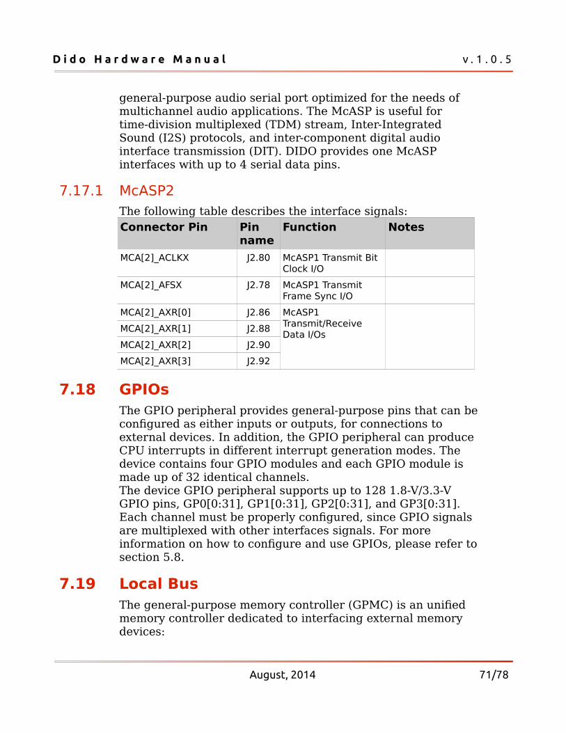
D i d o H a r d w a r e M a n u a l v . 1 . 0 . 5
general-purpose audio serial port optimized for the needs of multichannel audio applications. The McASP is useful for time-division multiplexed (TDM) stream, Inter-Integrated Sound (I2S) protocols, and inter-component digital audio interface transmission (DIT). DIDO provides one McASP interfaces with up to 4 serial data pins.
7.17.1 McASP2The following table describes the interface signals:Connector Pin Pin
nameFunction Notes
MCA[2]_ACLKX J2.80 McASP1 Transmit Bit Clock I/O
MCA[2]_AFSX J2.78 McASP1 Transmit Frame Sync I/O
MCA[2]_AXR[0] J2.86 McASP1 Transmit/Receive Data I/Os
MCA[2]_AXR[1] J2.88
MCA[2]_AXR[2] J2.90
MCA[2]_AXR[3] J2.92
7.18 GPIOsThe GPIO peripheral provides general-purpose pins that can beconfigured as either inputs or outputs, for connections to external devices. In addition, the GPIO peripheral can produce CPU interrupts in different interrupt generation modes. The device contains four GPIO modules and each GPIO module is made up of 32 identical channels.The device GPIO peripheral supports up to 128 1.8-V/3.3-V GPIO pins, GP0[0:31], GP1[0:31], GP2[0:31], and GP3[0:31]. Each channel must be properly configured, since GPIO signals are multiplexed with other interfaces signals. For more information on how to configure and use GPIOs, please refer to section 5.8.
7.19 Local BusThe general-purpose memory controller (GPMC) is an unified memory controller dedicated to interfacing external memory devices:
August, 2014 71/78
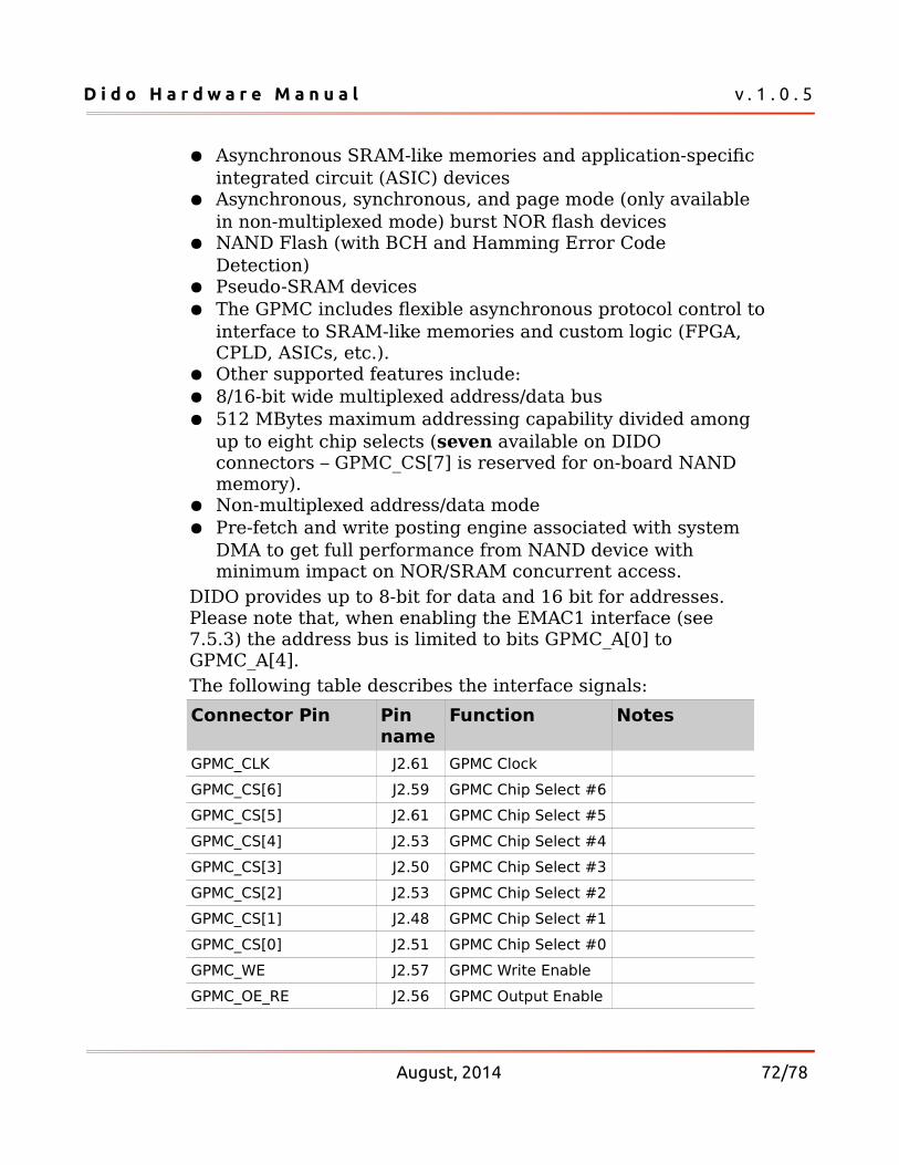
D i d o H a r d w a r e M a n u a l v . 1 . 0 . 5
Asynchronous SRAM-like memories and application-specific integrated circuit (ASIC) devices
Asynchronous, synchronous, and page mode (only available in non-multiplexed mode) burst NOR flash devices
NAND Flash (with BCH and Hamming Error Code Detection)
Pseudo-SRAM devices The GPMC includes flexible asynchronous protocol control to
interface to SRAM-like memories and custom logic (FPGA, CPLD, ASICs, etc.).
Other supported features include: 8/16-bit wide multiplexed address/data bus 512 MBytes maximum addressing capability divided among
up to eight chip selects (seven available on DIDO connectors – GPMC_CS[7] is reserved for on-board NAND memory).
Non-multiplexed address/data mode Pre-fetch and write posting engine associated with system
DMA to get full performance from NAND device with minimum impact on NOR/SRAM concurrent access.
DIDO provides up to 8-bit for data and 16 bit for addresses. Please note that, when enabling the EMAC1 interface (see7.5.3) the address bus is limited to bits GPMC_A[0] to GPMC_A[4].The following table describes the interface signals:
Connector Pin Pin name
Function Notes
GPMC_CLK J2.61 GPMC Clock
GPMC_CS[6] J2.59 GPMC Chip Select #6
GPMC_CS[5] J2.61 GPMC Chip Select #5
GPMC_CS[4] J2.53 GPMC Chip Select #4
GPMC_CS[3] J2.50 GPMC Chip Select #3
GPMC_CS[2] J2.53 GPMC Chip Select #2
GPMC_CS[1] J2.48 GPMC Chip Select #1
GPMC_CS[0] J2.51 GPMC Chip Select #0
GPMC_WE J2.57 GPMC Write Enable
GPMC_OE_RE J2.56 GPMC Output Enable
August, 2014 72/78
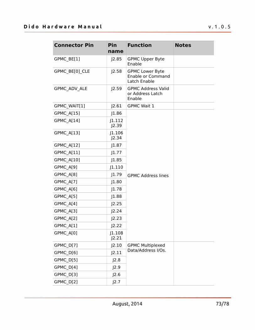
D i d o H a r d w a r e M a n u a l v . 1 . 0 . 5
Connector Pin Pin name
Function Notes
GPMC_BE[1] J2.85 GPMC Upper Byte Enable
GPMC_BE[0]_CLE J2.58 GPMC Lower Byte Enable or Command Latch Enable
GPMC_ADV_ALE J2.59 GPMC Address Valid or Address Latch Enable
GPMC_WAIT[1] J2.61 GPMC Wait 1
GPMC_A[15] J1.86
GPMC Address lines
GPMC_A[14] J1.112J2.39
GPMC_A[13] J1.106J2.34
GPMC_A[12] J1.87
GPMC_A[11] J1.77
GPMC_A[10] J1.85
GPMC_A[9] J1.110
GPMC_A[8] J1.79
GPMC_A[7] J1.80
GPMC_A[6] J1.78
GPMC_A[5] J1.88
GPMC_A[4] J2.25
GPMC_A[3] J2.24
GPMC_A[2] J2.23
GPMC_A[1] J2.22
GPMC_A[0] J1.108J2.21
GPMC_D[7] J2.10 GPMC Multiplexed Data/Address I/Os.GPMC_D[6] J2.11
GPMC_D[5] J2.8
GPMC_D[4] J2.9
GPMC_D[3] J2.6
GPMC_D[2] J2.7
August, 2014 73/78
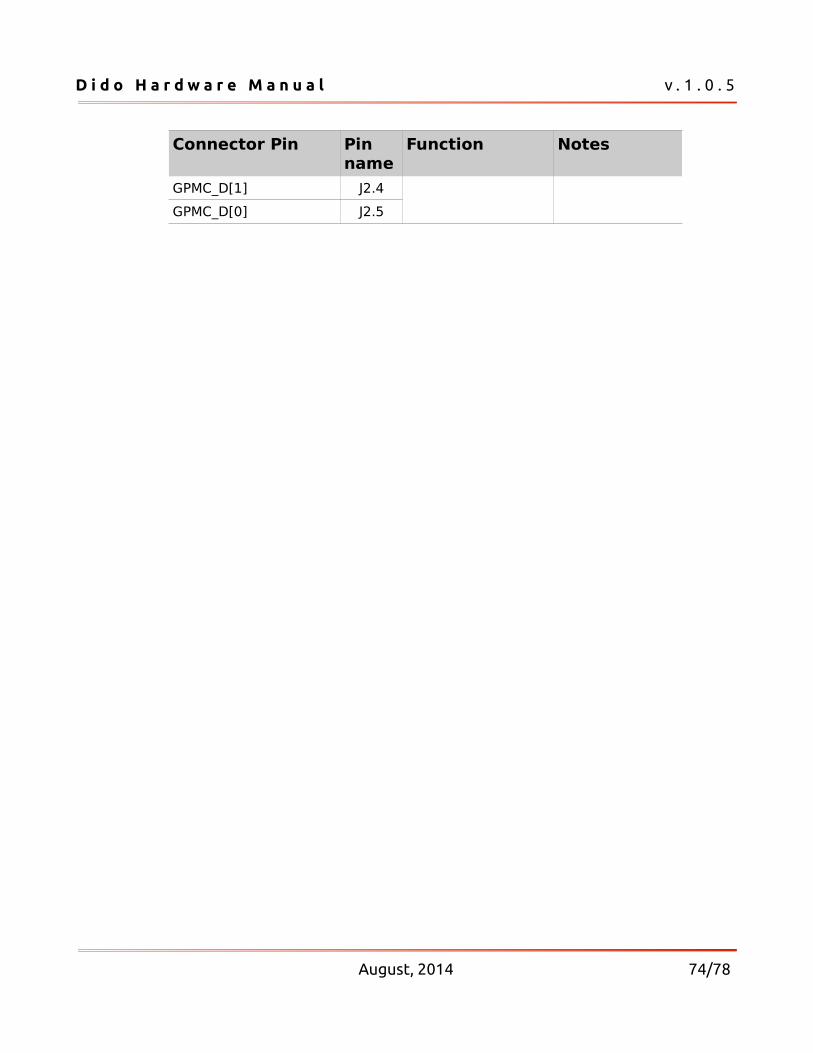
D i d o H a r d w a r e M a n u a l v . 1 . 0 . 5
Connector Pin Pin name
Function Notes
GPMC_D[1] J2.4
GPMC_D[0] J2.5
August, 2014 74/78
D i d o H a r d w a r e M a n u a l v . 1 . 0 . 5
8 Operational characteristics
8.1 Maximum ratingsThis section will be completed in a future version of this manual.Parameter Min Typ Max Unit
Main power supply voltage 3.1 3.3 V
8.2 Recommended ratingsThis section will be completed in a future version of this manual.Parameter Min Typ Max Unit
Main power supply voltage - 3.3 - V
8.3 Power consumptionProviding theoretical maximum power consumption value would be useless for the majority of system designers building their application upon DIDO module because, in most cases, this would lead to an over-sized power supply unit.Several configurations have been tested in order to provide figures that are measured on real-world use cases instead. Please note that DIDO platform is so flexible that it is virtually impossible to test for all possible configurations and applications on the market. The use cases here presented should cover most of real-world scenarios. However actual customer application might require more power than values reported here. Generally speaking, application specific requirements have to be taken into consideration in order to size power supply unit and to implement thermal management properly.
August, 2014 75/78
D i d o H a r d w a r e M a n u a l v . 1 . 0 . 5
8.3.1 Set 1Measurements have been performed on the following platform: NAON SOM (DM8148 model)
carrier board: NAONEVB-Lite
System software: NELK 1.0.0
Power monitor: INA226 (reference U20 of [[NAONEVB-Lite]] schematics).
ARM Cortex-A8 frequency: 600 MHz
SDRAM size: 512 MByte
SDRAM frequency: 400 MHz
HDVICP2 frequency: 306 MHz
8.3.2 Use cases
Checkpoint InputVoltage
ShuntVoltage
Current PowerConsumpion
Linux prompt (M3 unloaded)
3266 mV 8 mV 779 mA 2550 mW
Linux prompt (M3 loaded)
3261 mV 10 mV 1040 mA 3400 mW
cpuBurnA8 (M3 Loaded)
3258 mV 12 mV 1235 mA 3900 mW
decode & display H264 1080p60 on HDMI
3258 mV 12 mV 1219 mA 3975 mW
decode & display H264 1080p60 + cpuBurnA8
3255 mV 14 mV 1352 mA 4450 mW
Additional notes and reference: M3 Unloaded means that the two Cortex-M3 firmware has
not yet been started.
For decode/display test the sample application included in the TI EZSDK has been used.
Cpuburn heavily uses Cortex-A8 and Neon to maximize
August, 2014 76/78
D i d o H a r d w a r e M a n u a l v . 1 . 0 . 5
power consumption and heat spreading. See the debian package information (burnCortexA8.s) for further information.
Please note that shunt voltage value is rounded.
Please note that, although the NAON module has been used during these tests, usage of the DIDO module would lead to comparable results.
8.4 Heat DissipationThis section will be completed in a future version of this manual.
August, 2014 77/78
D i d o H a r d w a r e M a n u a l v . 1 . 0 . 5
9 Application notesPlease refer to the following documents available on DAVE Embedded Systems Developers Wiki:
Document Location
Integration Guide http://wiki.dave.eu/index.php/Integration_guide_%28Dido%29
Carrier board design guidelines
http://wiki.dave.eu/index.php/Carrier_board_design_guidelines_%28SOM%29
August, 2014 78/78