application note an-8005 -...
TRANSCRIPT
Application Note
Revision:
Issue Date:
Prepared by:
00
2008-09-24
Frédéric Sargos
IGBT Power Electronics Teaching SystemPrinciple for sizing power converters
AN-8005
1 / 1 72008-09-24 – Rev00© by SEMIKRON
Inside the box .......................................................................................................................................................................2 Very important safety recommendations...........................................................................................................................2 The interfaces / connectors.................................................................................................................................................2 Preliminary remark .................................................................................................................................................................2 How to integrate the stack in the application ..........................................................................................................................3 The components of the power electronics teaching system............................................................................................3 The heat sink and the fan .......................................................................................................................................................3 The drivers .............................................................................................................................................................................3 The rectifier SKD 51/14 ..........................................................................................................................................................5 The IGBT modules SKM 50 GB 123 D...................................................................................................................................5 The filtering capacitors ...........................................................................................................................................................5 Why is the current limited in the capacitors ? ..................................................................................................................5 How to put capacitors in series? .....................................................................................................................................5 The switching cell ...................................................................................................................................................................6 The snubber capacitors...................................................................................................................................................7 The bus bar .....................................................................................................................................................................7 The thermal protection devices ..............................................................................................................................................8 The Normally-On thermal contact switch.........................................................................................................................8 The temperature sensor ..................................................................................................................................................8 The IGBT (Insulated Gate Bipolar Transistor) module......................................................................................................8 Switching the IGBT.................................................................................................................................................................9 Snubber or snubberless ......................................................................................................................................................10 The IGBT in short-circuit.......................................................................................................................................................10 The calculations of losses.................................................................................................................................................10 The origin of losses ..............................................................................................................................................................10 Why are power losses a problem? .......................................................................................................................................12 The conduction losses..........................................................................................................................................................12 Application example: Buck Chopper with DC output current .........................................................................................12 Application example: 3 phase PWM inverter.................................................................................................................13 The switching losses ............................................................................................................................................................13 Application example: Buck Chopper with DC output current .........................................................................................14 Application example: 3 phase PWM inverter.................................................................................................................14 From losses calculation to temperatures estimation......................................................................................................14 Modelling – thermal-electrical equivalence...........................................................................................................................16 References ..........................................................................................................................................................................16 Annex - SKHI 22 AR data-sheet.........................................................................................................................................17
Application Note AN-8005
2 / 17 2008-09-24 – Rev00 © by SEMIKRON
Inside the box Before unpacking, please ensure that the following elements are inside the box. • The stack itself • A test certificate, which is a guarantee of safe working of the stack • The technical description Very important safety recommendations To avoid damage to the converter and for the safety of the operator, it is strongly recommended to follow these instructions: Always monitor the voltage at the capacitor bank. It must never exceed the maximum value of 750 Vdc, as there is no protection against DC over-voltage embedded in the Power Electronics Teaching Unit. After the tests, the capacitors may remain charged for a couple of minutes. One must anticipate that the DC voltage limit shall never be exceeded when designing a control unit board. When powering the unit, a pre-charging device (a choke or a resistance) should be inserted to prevent very high
charge currents. Never carry or move the device while it is electrically connected to anything. The error signal from the drivers must be taken into account in the control process. When connecting the command signals, it is preferable to use a anti-static protection bracelet. Never exceed the maximum allowed current (30 A). Connect a circuit breaker between the supply voltage and the converter. A thermal contact switch has been placed in the heat sink, close to the warmest point, to disconnect the circuit in case of abnormal heating of the heat sink. As a protection device, it should be connected in series with the driver power supply.
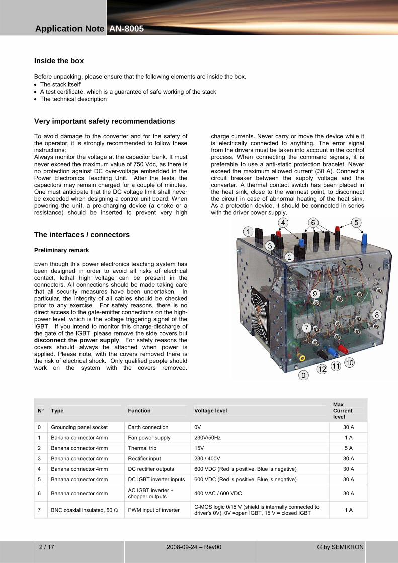
The interfaces / connectors Preliminary remark Even though this power electronics teaching system has been designed in order to avoid all risks of electrical contact, lethal high voltage can be present in the connectors. All connections should be made taking care that all security measures have been undertaken. In particular, the integrity of all cables should be checked prior to any exercise. For safety reasons, there is no direct access to the gate-emitter connections on the high-power level, which is the voltage triggering signal of the IGBT. If you intend to monitor this charge-discharge of the gate of the IGBT, please remove the side covers but disconnect the power supply. For safety reasons the covers should always be attached when power is applied. Please note, with the covers removed there is the risk of electrical shock. Only qualified people should work on the system with the covers removed.
N° Type Function Voltage level Max Current level
0 Grounding panel socket Earth connection 0V 30 A
1 Banana connector 4mm Fan power supply 230V/50Hz 1 A
2 Banana connector 4mm Thermal trip 15V 5 A
3 Banana connector 4mm Rectifier input 230 / 400V 30 A
4 Banana connector 4mm DC rectifier outputs 600 VDC (Red is positive, Blue is negative) 30 A
5 Banana connector 4mm DC IGBT inverter inputs 600 VDC (Red is positive, Blue is negative) 30 A
6 Banana connector 4mm AC IGBT inverter + chopper outputs 400 VAC / 600 VDC 30 A
7 BNC coaxial insulated, 50 Ω PWM input of inverter C-MOS logic 0/15 V (shield is internally connected to driver’s 0V), 0V =open IGBT, 15 V = closed IGBT 1 A
Application Note AN-8005
3 / 172008-09-24 – Rev00© by SEMIKRON
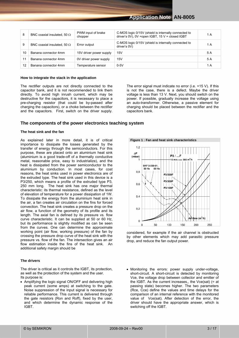
8 BNC coaxial insulated, 50 Ω PWM input of brake chopper
C-MOS logic 0/15V (shield is internally connected to driver’s 0V), 0V =open IGBT, 15 V = closed IGBT 1 A
9 BNC coaxial insulated, 50 Ω Error output C-MOS logic 0/15V (shield is internally connected to driver’s 0V) 1 A
10 Banana connector 4mm 15V driver power supply 15V 5 A
11 Banana connector 4mm 0V driver power supply 15V 5 A
12 Banana connector 4mm Temperature sensor 0-5V 1 A
How to integrate the stack in the application The rectifier outputs are not directly connected to the capacitor bank, and it is not recommended to link them directly. To avoid high inrush current, which may be destructive for the capacitors, it is necessary to place a pre-charging resistor (that could be by-passed after charging the capacitors), or a choke between the rectifier and the capacitors. First, switch on the driver supply.
The error signal must indicate no error (i.e. +15 V). If this is not the case, there is a defect. Maybe the driver voltage is less than 13 V. Next, you should switch on the power. If possible, gradually increase the voltage using an auto-transformer. Otherwise, a passive element for charging should be placed between the rectifier and the capacitors bank.
The components of the power electronics teaching system The heat sink and the fan As explained later in more detail, it is of critical importance to dissipate the losses generated by the transfer of energy through the semiconductors. For this purpose, these are placed onto an aluminium heat sink (aluminium is a good trade-off of a thermally conductive metal, reasonable price, easy to industrialize), and the heat is dissipated from the power semiconductor to the aluminium by conduction. In most cases, for cost reasons, the heat sinks used in power electronics are of the extruded type. The heat sink used in this device is a P3/250, which means a profile of the extruded type P3, 250 mm long. The heat sink has one major thermal characteristic: its thermal resistance, defined as the level of elevation of temperature for a power dissipation of 1W. To dissipate the energy from the aluminium heat sink in the air, a fan creates air circulation on the fins for forced convection. The heat sink creates a pressure drop on the air flow, a function of the geometry of its profile and its length. The axial fan is defined by its pressure vs. flow curve characteristic. It can be supplied at 50 or 60 Hz, but its performance is slightly modified as can be seen from the curves. One can determine the approximate working point (air flow, working pressure) of the fan by crossing the pressure drop curve of the heat sink with the pressure vs. flow of the fan. The intersection gives an air flow estimation inside the fins of the heat sink. An additional safety margin should be
considered, for example if the air channel is obstructed by other elements which may add parasitic pressure drop, and reduce the fan output power.
The drivers The driver is critical as it controls the IGBT, its protection, as well as the protection of the system and the user. Its purpose is: • Amplifying the logic signal ON/OFF and delivering high
peak current (some amps) at switching to the gate. Noise suppression of the input signal is necessary for reliable performance. This current is delivered through the gate resistors (Ron and Roff), fixed by the user, and which determine the dynamic response of the IGBT.
• Monitoring the errors: power supply under-voltage, short-circuit. A short-circuit is detected by monitoring Vce, the voltage drop between collector and emitter of the IGBT. As the current increases,, the Vce(sat) (= at passing state) becomes higher. The two parameters (Rce, Cce) define the values and time delays for the comparison of an internal reference with the monitored value of Vce(sat). After detection of the error, the driver should have the appropriate answer, which is switching off the IGBT.
Figure 1 : Fan and heat sink characteristics
Application Note AN-8005
4 / 17 2008-09-24 – Rev00 © by SEMIKRON
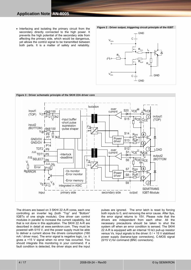
• Interfacing and isolating the primary circuit from the
secondary directly connected to the high power. It prevents the high potential of the secondary side from affecting the primary side, which would be dangerous, yet allows the control signal to be transmitted between both parts. It is a matter of safety and reliability.
Figure 3 : Driver schematic principle of the SKHI 22A driver core
The drivers are based on 3 SKHI 22 A-R cores, each one controlling an inverter leg (both “Top” and “Bottom” IGBTs of one single module). One driver can control modules in parallel to increase the current capability, but that is not done in this application. The SKHI 22 A-R are described in detail at www.semikron.com. They must be powered with 0/15 V, and the power supply must be able to deliver a current above the drivers consumption (160 mA / driver max). The error signal is negative logic, i.e. it gives a +15 V signal when no error has occurred. You should integrate this monitoring in your command. If a fault condition is detected, the driver stops and the input
pulses are ignored. The error latch is reset by forcing both inputs to 0, and removing the error cause. After 9µs, the error signal returns to 15V. Please note that the drivers are independent from each other. All the necessary precautions should be taken to shut the system off when an error condition is sensed. The SKHI 22 A-R is equipped with an internal 10 kΩ pull-up resistor versus Vs. Input signals to the driver: 0 / + 15 V stabilised power supply (banana-type connectors), C-MOS signal (0/15 V) for command (BNC connectors).
Figure 2 : Driver output, triggering circuit principle of the IGBT
Application Note AN-8005
5 / 172008-09-24 – Rev00© by SEMIKRON
The rectifier SKD 51/14 This is a 3 phase diode-rectifier, isolated power module. It should not be used for a network higher than 440VAC. This rectifier can be used in single phase configuration also, by leaving one branch of the rectifier disconnected. The IGBT modules SKM 50 GB 123 D Each of these modules is an inverter leg, and is made of 2 IGBTs with an anti-parallel diode, connected in series, of which the middle point is at terminal 1. The top IGBT collector is at terminal 3 and the bottom IGBT emitter is at terminal 2. The IGBTs are forced closed by a 15V signal between the gate (terminals 4 -resp 6) and the associated emitter (gate 5 –resp 7) and forced open by a –15 V order on the same terminals. These control signal voltages are delivered by the SKHI 22 AR, driver core through an additional gate resistor whose value is 30 Ohms. These resistors are soldered on the printed circuit board of the drivers. The purpose for this resistor is to limit the charging current of the gate, and consequently, the collector-emitter over-voltages commensurate to the parasitic inductance. Conversely a higher gate resistance increases the switching losses. The chosen value is always a trade-off between protection of the IGBT and the admissible losses. Moreover, the choice of this value will have a significant influence on the dV/dt spectrum, which has a real influence on the EMC characteristics of the converter. The choice of a gate resistor is of critical importance. The filtering capacitors The filtering capacitors are electrolytic capacitors, their individual value is 2200 µF/400 V, 2 connected in series, 2 in parallel. The equivalent capacitor of the complete DC bus is 1100µF/800 V. Theoretically, this value is to be determined by the desired filtering quality (capacitance / voltage) . Practically, for electrolytic technology, the RMS current admissible in the capacitors is the main sizing parameter, and manufacturers often place more capacitors than required just because of current limitation on the capacitors. The value of the current depends on the application, and the maximum allowed value by the capacitors is 19,1 A at 40°C or 8,2 A at 85°C. Our experience shows that this sizing fulfils almost all applications in the range of power addressed by the Power Electronics Teaching System. Why is the current limited in the capacitors The equivalent model of a capacitor is given below. For a given current, the losses are approximately Rs.I², and heat up the core of the capacitors.The LTE (Life Time Expectancy) is highly dependant on the hot spot temperature, according to a rule of the type,
KT Ths
⋅−
2 10( max )
where TMax is the maximum temperature allowed, and Ths the Hot Spot Temperature (inside temperature). Reaching an internal value of more than 85-90°C may not only considerably reduce the lifetime of the product, but may also lead to explosion risks. There are different capacitor technologies, but today the electrolytic type is the best fitted to the range of power and voltage of most applications in power electronics (from 1 kW to 1 MW and 200 VDC to 1000
VDC). This is due to their high capacitance, high voltage and medium current. Their main limitations come from a relatively high internal resistance Rse, which limits the RMS current – which has a direct effect on the lifetime. Some mounting technologies propose to dissipate the heat from inside the capacitor to a heat sink, or by creating an air circulation around the capacitors. How to put capacitors in series When forcing a constant voltage to ideal capacitors put in series, the capacitor can be considered as an open circuit, and the voltage should be equally shared between the capacitors. However, a parasitic leakage resistor (Rleak) causes a leakage current inside the capacitors at no load. In the case of 2 capacitors in series (or more), the equivalent model will then be a dividing bridge whose voltages are defined by the ratio of the leakage resistances in series. As the values Rleak are highly variable, since they are a consequence of imperfections in the capacitor and the manufacturing process, the voltages may vary widely, leading to a dangerous steady state DC voltage on one capacitor. Attention: Applying a DC voltage higher than its rated voltage to an electrolytic capacitor may lead to its destruction by explosion. To avoid differences in the voltage across capacitors, each capacitor must be connected in parallel to a balancing resistor, whose value must be much smaller than Rleak (about 1/10th). This resistor value is more accurate and stable, hence the voltage balance is much better. The principle of no-load charging is shown here below, using a realistic 50% internal parasitic resistance difference.
Figure 5 : SKM 50 GB 123 D, dual IGBT module
Figure 4 : The SKD 51 rectifier module
Figure 6 : 1st order equivalent electrical model of an electrolytic capacitor

Application Note AN-8005
6 / 17 2008-09-24 – Rev00 © by SEMIKRON
Figure7 : Voltage sharing without balancing resistors
Figure 8 : With balancing resistors
Moreover, for safety purposes, these resistors discharge the capacitors when no energy is supplied to the capacitors from the network, or the load. However, it is highly recommended to have a discharging device, since the discharge time constant of the capacitor is 22 kΩ x 2200 µF = 46.2 s. The switching cell If high currents are switched fast then voltage overshoots occur which can destroy the switching power
semiconductor if these overshoots exceed the maximum rated voltage (here 1200V).
Figure 9 : Top IGBT ON Figure 10 : Top IGBT turned OFF
IGBT Module
DC+
DC-
AC
L C
L E
LSnubber
LDC+
LDC-
CDC-link
LESR
RESR
CSnubber
iL
IGBT Module
DC+
DC-
AC
L C
L E
LSnubber
LDC+
LDC-
CDC-link
LESR
RESR
CSnubber
iL
Energy is stored in the parasitic inductances
DC+
DC-
AC
IGBT Module
L C
L E
LSnubber
LDC+
LDC-
CDC-link
LESR
RESR
CSnubber
iL
Vce overshoot
Energy needs to be dissipated
DC+
DC-
AC
IGBT Module
L C
L E
LSnubber
LDC+
LDC-
CDC-link
LESR
RESR
CSnubber
iL
DC+
DC-
AC
IGBT Module
L C
L E
LSnubber
LDC+
LDC-
CDC-link
LESR
RESR
CSnubber
iL
Vce overshoot
Energy needs to be dissipated
This voltage overshoot is caused by the energy stored in the magnetic field of the current path (e.g. DC-link connections). It is linked by the value of the total parasitic inductance or stray inductance LS (E=0,5*LS*i²). LS is the sum of all parasitic inductances. The voltage (V=LS*di/dt) may exceed the maximum blocking voltage of the power semiconductor (VCES, VRRM…) because it is added to the DC link voltage. The first countermeasure is a good low inductive DC link design (the DC bus bar) to keep the
voltage applied on the semiconductor low. This is done by means of a laminated bus bar system (sandwich of +DC, –DC metal sheets and an insulation layer between) and short connections between the voltage source (DC-link capacitor) and power semiconductor. In addition, snubber capacitors are recommended, which should be mounted directly on the DC-link terminals of each IGBT module. This snubber works as a low-pass filter and “suppresses” the voltage overshoot.
Application Note AN-8005
7 / 172008-09-24 – Rev00© by SEMIKRON
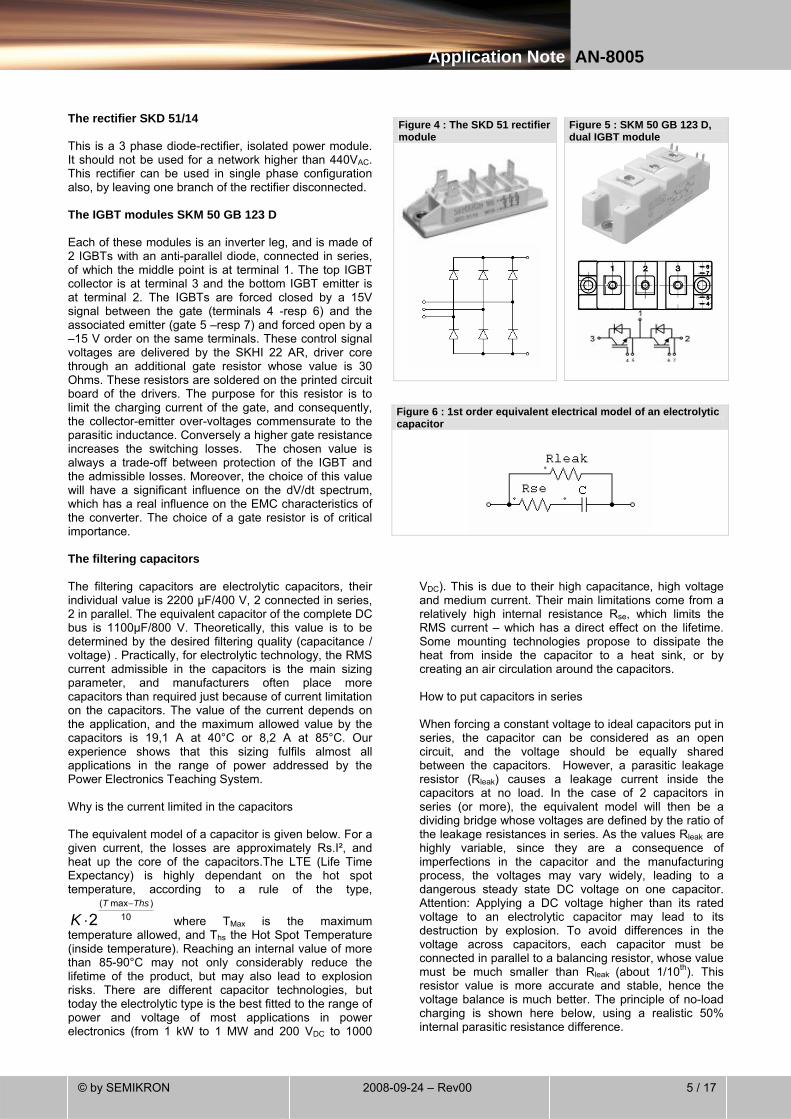
The snubber capacitors They are placed as close to the IGBT module as possible to minimize the inductance between the switches and the capacitor. The waveform below shows a comparison of the voltage across an IGBT at turn-off, with and without snubber capacitor. The effect of voltage spike reduction
can be clearly seen.The snubbers limit the over-voltages during commutations and as a consequence reduce the losses. They also protect the semiconductors against destructive overshoots during short-circuits cut-off.
The bus bar A low inductance laminated bus bar is used to connect the DC link capacitors to the inverter. The DC capacitors should be considered as a pure voltage source. Therefore the construction of the bus bar must have the minimum level of parasitic inductance. The laminated bus
bar is made of 2 conductive metal plates (DC+ and DC-), with a large surface facing each other, separated by a thin isolating film, their inductance is much smaller than a wire connection.
In practice, the inductance of the bus bar can be derived from the overshoot of VCE at switch-off.
Figure 11 : Typical waveform of VCE voltage on IGBT at switching off
Figure 12 : Low inductance snubber capacitors for mounting on IGBT modules
Figure 13 : Equivalent circuit diagram of IGBT module connected to DC-link and snubber capacitor
dt/diLV c1 ⋅Σ=Δ
dt/di)LLL(V cSnubberEC2 ⋅++=Δ
Snubber
2cLinkDC
3 CiLV ⋅
≤Δ −
SnubberLinkDC CL21
T1f
⋅⋅π⋅==
−
ESRDCDCEC LLLLLL ++++=Σ −+
ESRDCDCLinkDC LLLL ++= −+−
Black line : Without snubber Brown line : With snubber
VCE = 200V/dev 400ns/dev
Vcc �V3
�V1
T/2 �V1
�V2
DC+
DC-
AC Load
IGBT Module
IGBT Driver
L C
L E
LSnubber
LDC+
LDC-
CDC-link
LESR
RESR
CSnubber
TOP
BOT
DC+, DC-, AC IGBT module terminals L C, L E IGBT module parasitic inductance LDC+, LDC Bus bar parasitic inductance CSnubber Snubber capacitor capacitance
LSnubber Snubber capacitor series inductance CDC-link DC-link capacitor capacitance LESR, RESR DC-link capacitor parasitics
Application Note AN-8005
8 / 17 2008-09-24 – Rev00 © by SEMIKRON
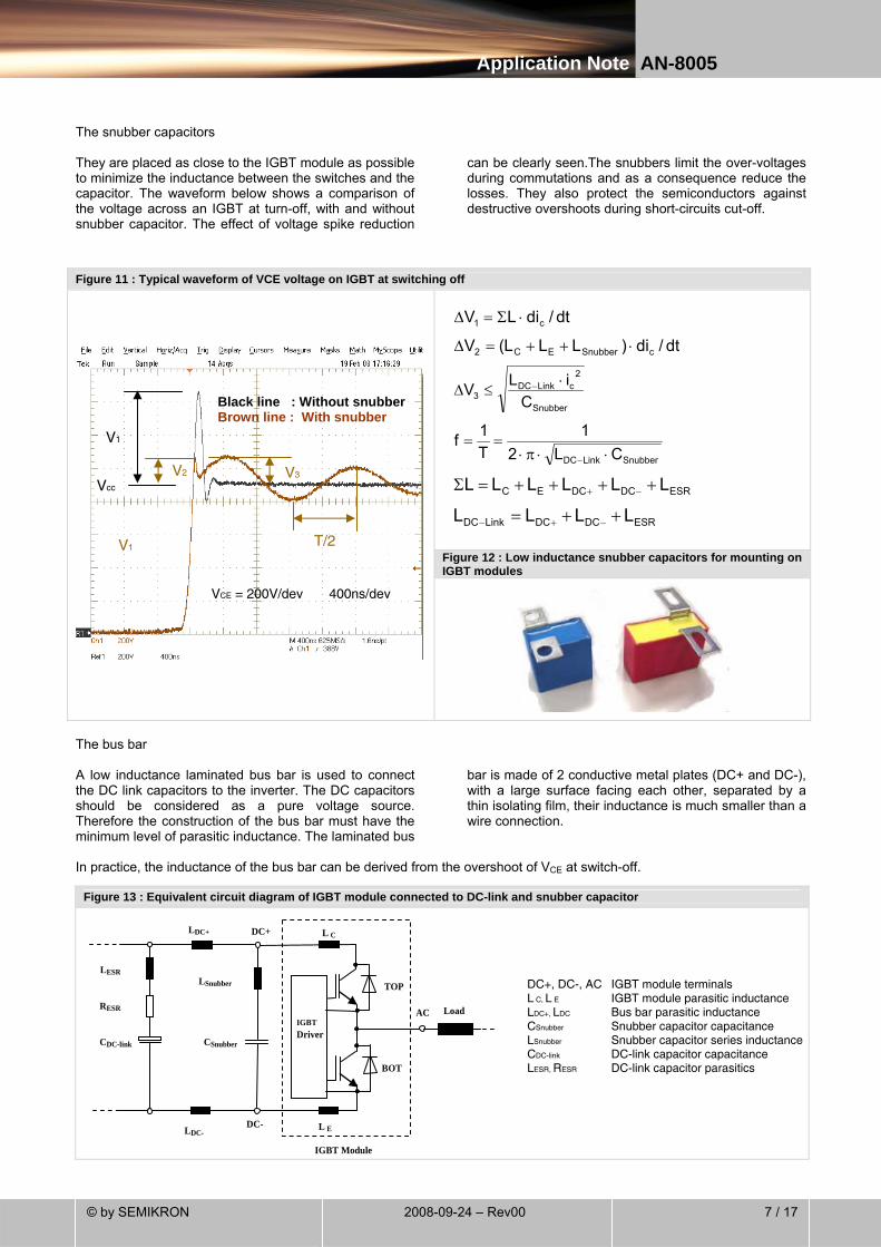
The thermal protection devices The Normally-On thermal contact switch Playing the role of a re-usable thermal fuse, this is an electrical contact, mechanically closed when its temperature is below the threshold temperature (71°C), and open when beyond. Practically, it is recommended to connect it in series with the driver power supply to stop the application in case of overheating. Its purpose is generally to detect the defect of the fan or abnormal long term current overload. After cooling down, it comes back to an ON position 20°C under its threshold value. The temperature sensor The LM335Z from National Semiconductor (see data-sheet link http://cache.national.com/ds/LM/LM335.pdf is an integrated circuit dedicated to precision temperature measurement. It is placed into the heat sink as close as possible to the heat source (the semiconductors). This measuring point serves as a reference point for heat sink temperature and it is referred to as Th. One possible application is to make an estimation of the power losses P, thanks to the formula RthTP ⋅Δ= , where ΔT is the temperature difference between the heat sink and the ambient air, and Rth is the thermal resistance of the heat sink P3/265F (96,2 K/kW). The voltage rise
across the probe is proportional to the temperature, in the range of 10 mV/°C. The curve on Figure should be re-calibrated at 25°C for better accuracy. The test certificate gives the voltage value for a given temperature, so the temperature Th can be identified at any instant.
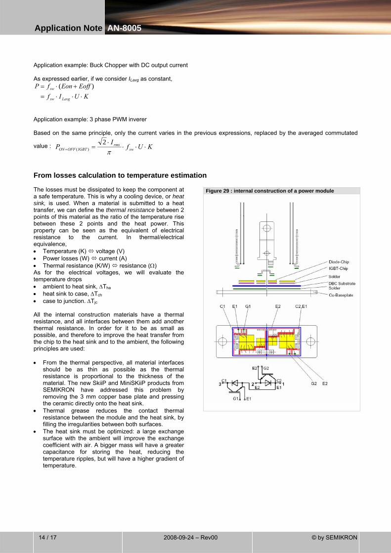
The IGBT (Insulated Gate Bipolar Transistor) module
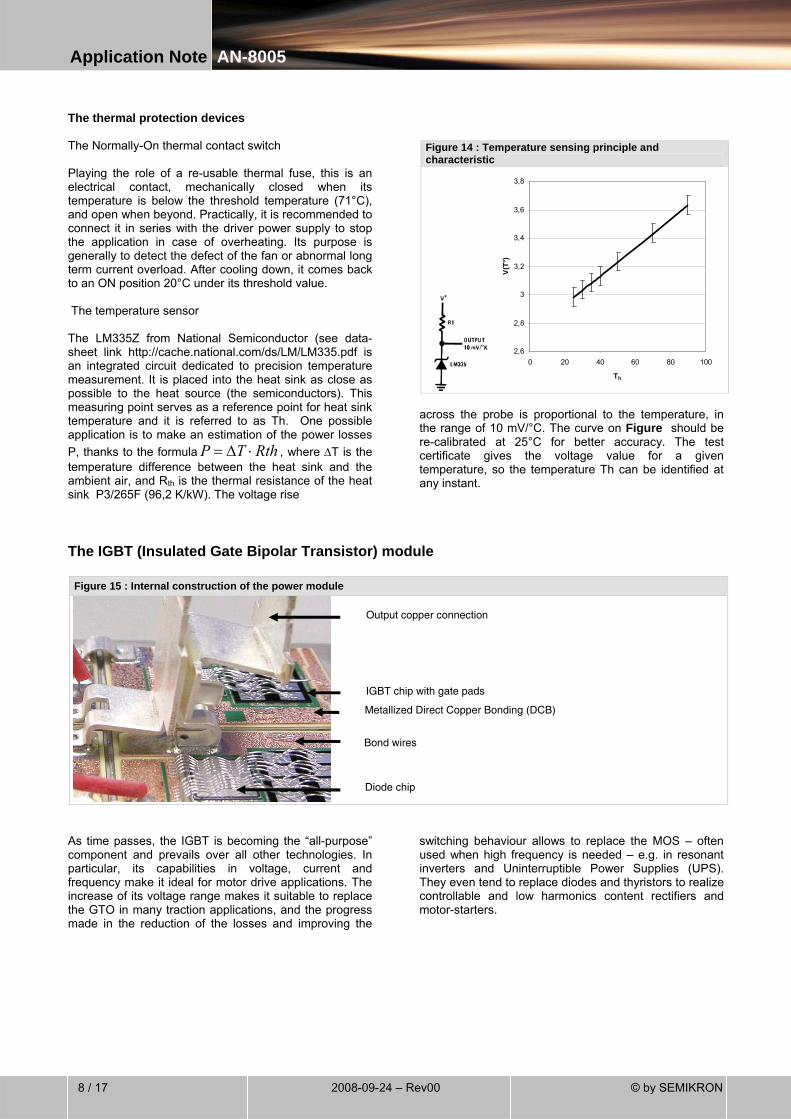
Figure 15 : Internal construction of the power module
As time passes, the IGBT is becoming the “all-purpose” component and prevails over all other technologies. In particular, its capabilities in voltage, current and frequency make it ideal for motor drive applications. The increase of its voltage range makes it suitable to replace the GTO in many traction applications, and the progress made in the reduction of the losses and improving the
switching behaviour allows to replace the MOS – often used when high frequency is needed – e.g. in resonant inverters and Uninterruptible Power Supplies (UPS). They even tend to replace diodes and thyristors to realize controllable and low harmonics content rectifiers and motor-starters.
Figure 14 : Temperature sensing principle and characteristic
2,6
2,8
3
3,2
3,4
3,6
3,8
0 20 40 60 80 100
Th
V(T
°)
Diode chip
Output copper connection
IGBT chip with gate pads
Metallized Direct Copper Bonding (DCB)
Bond wires

Application Note AN-8005
9 / 172008-09-24 – Rev00© by SEMIKRON
The reasons for its success come directly from its structure. • It is relatively easy to drive. Similar to the MOSFET, the IGBT is controlled by a voltage, not a current, the drivers have
become much simpler and cheaper compared with thyristors or BJTs for example. • For a given voltage class (600 V for example) and a given current, the IGBT chip is smaller than the MOS’s, as a
consequence the internal gate capacitance is smaller, hence the driver power supply is cheaper. In addition, the saturation voltage (voltage drop between collector and emitter of the transistor) is lower than that of the MOS.
• The IGBT can be turned ON and OFF. • Low firing current, average and instantaneous • Good trade-off (High voltage, high current, high frequency) • Short-circuit capability
Switching the IGBT The IGBT is triggered by charging the gate, which is done by applying a voltage across the gate and the emitter (Figure ). At first estimation, charging the IGBT can be approximated to charging an RC load, where R is roughly the gate resistor determined by the user and C is determined by the component structure. In power electronics, the IGBT transistor is used for switching, not for amplification, and especially for hard switching purposes. Therefore the IGBT works only in saturated mode. It is turned ON when the VGE voltage becomes higher than a threshold value (typically 5.5 V for the SKM 50 GB 123D). These modules are optimized for a –15/+15 V control signal, which the SKHI 22 A (driver) is able to deliver, to ensure the best dynamic response from the IGBT. Figure 19 : The gate charge characteristic
Turn-on: 0...t1 (blocked transistor) Gate current will be triggered by applying a control voltage. Up to the charge quantity QG1 the current iG solely charges the gate capacitance CGE. The gate voltage VGE rises. As VGE is still below the threshold voltage VGE(th), no gate current will flow during this period.
Turn-on: t1...t2 (rise of gate current) As soon as VGE has reached VGE(th)-level at t1, the transistor is turned on, first passing the active region. Gate current rises to IL-level (ideal free-wheeling diode) or even exceeds IL - as indicated in the switching pattern figure for a real free-wheeling diode. Similarly, VGE, which is connected to the collector current in the active region by the transconductance gfc with ID = gfc * VGE, will increase up to the value VGE1 = ID/gfC (time t2). Since the free-wheeling diode can block the current only at t2, VCE will not drop considerably up to t2. At t = t2 charge QG2 has flown into the gate.
Turn-on: switching interval t2...t3 (transistor during turn-on) When the free-wheeling diode is turned off, VCE will drop almost to on-state value VCE(on) by time t3. Between t2 and t3 drain current and gate-source voltage are still coupled by transconductance; herefore, VGE remains constant. While VCE is decreasing, the Miller capacitance CGC is recharged by the gate current iG with the charge quantity (QG3-QG2). By t = t3 charge QG3 has flown into the gate.
Turn-on: t3...t4 (saturation region) At t3 the transistor is turned on, its curve has passed the pinch-off area to enter the ohmic area. VGE and IC are no longer coupled by gfs. The charge conducted to the gate (QGtot-QG3) at this point affects a further increase of VGE up to the gate control voltage VGG-. Since the collector-emitter on-resistance RCE(on) depends on IC and VGE, the on-state voltage VCE(on) = IC * RCE(on) may be adjusted to the physical minimum by the total charge quantity QGtot conducted to the gate. The higher the collector-emitter voltage VCE (or commutation voltage), the bigger the charge QGtot required to reach a certain gate-emitter voltage, see VGE(QG) curve.
Turn-off During turn-off the described processes are running in reverse direction; the charge QGtot has to be conducted out of the gate by the control current. For approximations to determine the gate charge quantity required for turn-off, the gate charge characteristic in the VGE(QG) curve may be used.
Figure 16 : gate charge and discharge Vge (t), switching ON and OFF
Application Note AN-8005
10 / 17 2008-09-24 – Rev00 © by SEMIKRON
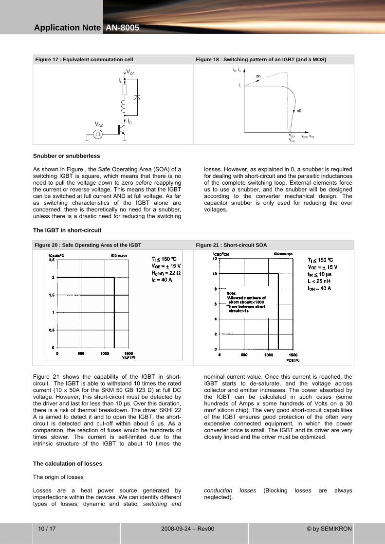
Figure 17 : Equivalent commutation cell Figure 18 : Switching pattern of an IGBT (and a MOS)
Snubber or snubberless As shown in Figure , the Safe Operating Area (SOA) of a switching IGBT is square, which means that there is no need to pull the voltage down to zero before reapplying the current or reverse voltage. This means that the IGBT can be switched at full current AND at full voltage. As far as switching characteristics of the IGBT alone are concerned, there is theoretically no need for a snubber, unless there is a drastic need for reducing the switching
losses. However, as explained in 0, a snubber is required for dealing with short-circuit and the parasitic inductances of the complete switching loop. External elements force us to use a snubber, and the snubber will be designed according to the converter mechanical design. The capacitor snubber is only used for reducing the over voltages.
The IGBT in short-circuit
Figure 20 : Safe Operating Area of the IGBT Figure 21 : Short-circuit SOA
Figure 21 shows the capability of the IGBT in short-circuit. The IGBT is able to withstand 10 times the rated current (10 x 50A for the SKM 50 GB 123 D) at full DC voltage. However, this short-circuit must be detected by the driver and last for less than 10 µs. Over this duration, there is a risk of thermal breakdown. The driver SKHI 22 A is aimed to detect it and to open the IGBT; the short-circuit is detected and cut-off within about 5 µs. As a comparison, the reaction of fuses would be hundreds of times slower. The current is self-limited due to the intrinsic structure of the IGBT to about 10 times the
nominal current value. Once this current is reached, the IGBT starts to de-saturate, and the voltage across collector and emitter increases. The power absorbed by the IGBT can be calculated in such cases (some hundreds of Amps x some hundreds of Volts on a 30 mm² silicon chip). The very good short-circuit capabilities of the IGBT ensures good protection of the often very expensive connected equipment, in which the power converter price is small. The IGBT and its driver are very closely linked and the driver must be optimized.
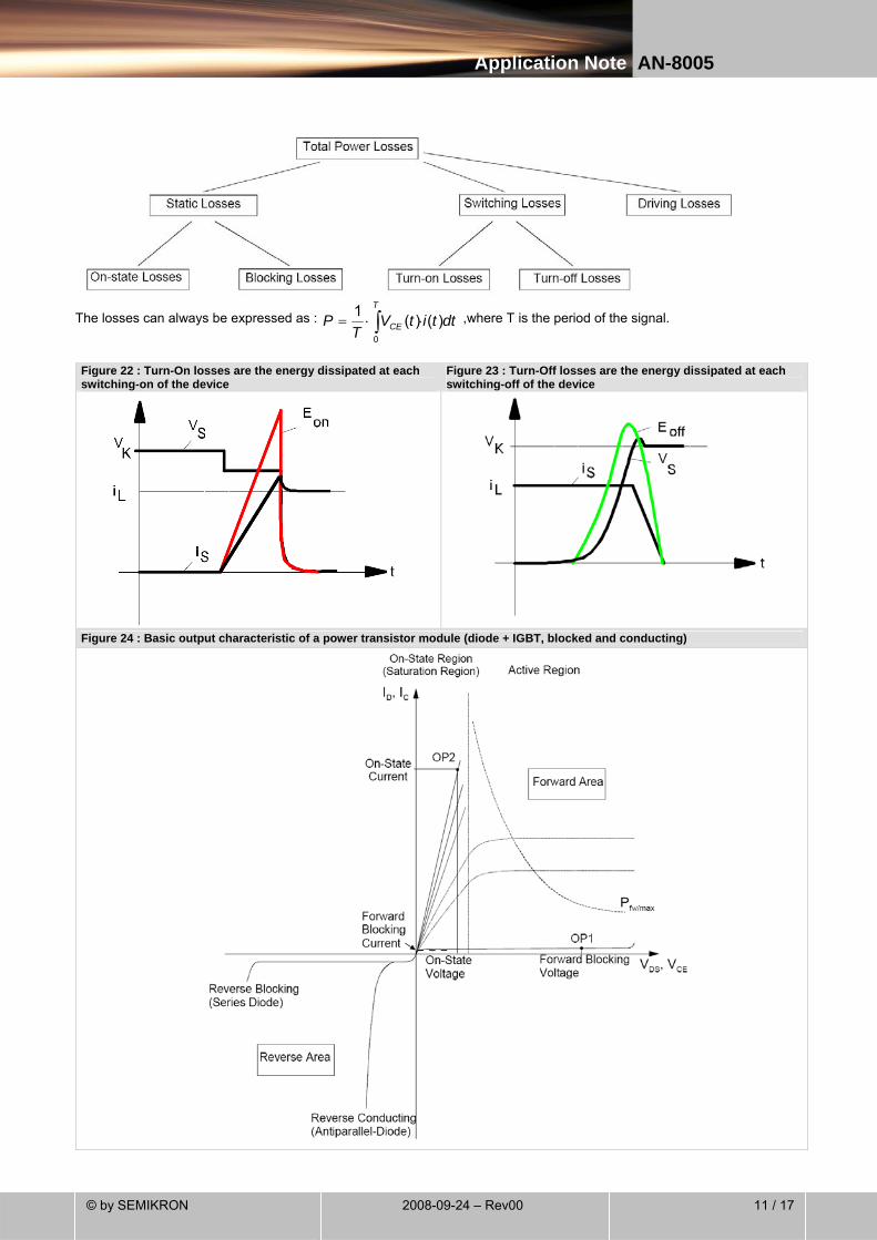
The calculation of losses The origin of losses Losses are a heat power source generated by imperfections within the devices. We can identify different types of losses; dynamic and static, switching and
conduction losses (Blocking losses are always neglected).
Application Note AN-8005
11 / 172008-09-24 – Rev00© by SEMIKRON
The losses can always be expressed as : PT
V t i t dtCE
T
= ⋅ ⋅∫1
0
( ) ( ) ,where T is the period of the signal.
Figure 22 : Turn-On losses are the energy dissipated at each switching-on of the device
Figure 23 : Turn-Off losses are the energy dissipated at each switching-off of the device
Figure 24 : Basic output characteristic of a power transistor module (diode + IGBT, blocked and conducting)
Application Note AN-8005
12 / 17 2008-09-24 – Rev00 © by SEMIKRON
Why are power losses a problem One of the main challenges for the power electronics designer is to deal with the thermal aspect. Due to semiconductor imperfections, a semiconductor can never be a pure switch (infinite resistance when OFF, zero when ON). When a device sees a voltage difference and a current circulates through it, power losses are generated which appear as heat, and must be removed as efficiently as possible. It is generally identified that the silicon temperature, called junction temperature, Tj, shall never reach or surpass the maximum allowed Tjmax. Beyond this Tjmax, there is a great risk of failure in the bond wire connections, also the electrical characteristics of the component can change (e.g. rise of the leakage
current in the open IGBT): there is also a risk of destruction. This Tjmax is typically 150°C. Taking into account the disparity of components (although the process has become more and more reliable and some devices can reach today higher temperatures), one should respect a safety margin. On the other hand, taking too much safety margin is detrimental to the economic margin since it would mean more silicon, therefore higher cost. For the IGBTs, it is safe and economically viable to respect a 125°C maximum junction temperature. In addition to that, losses reduce the overall efficiency. It is usual to reach 95% to 98% efficiency with IGBT converters.
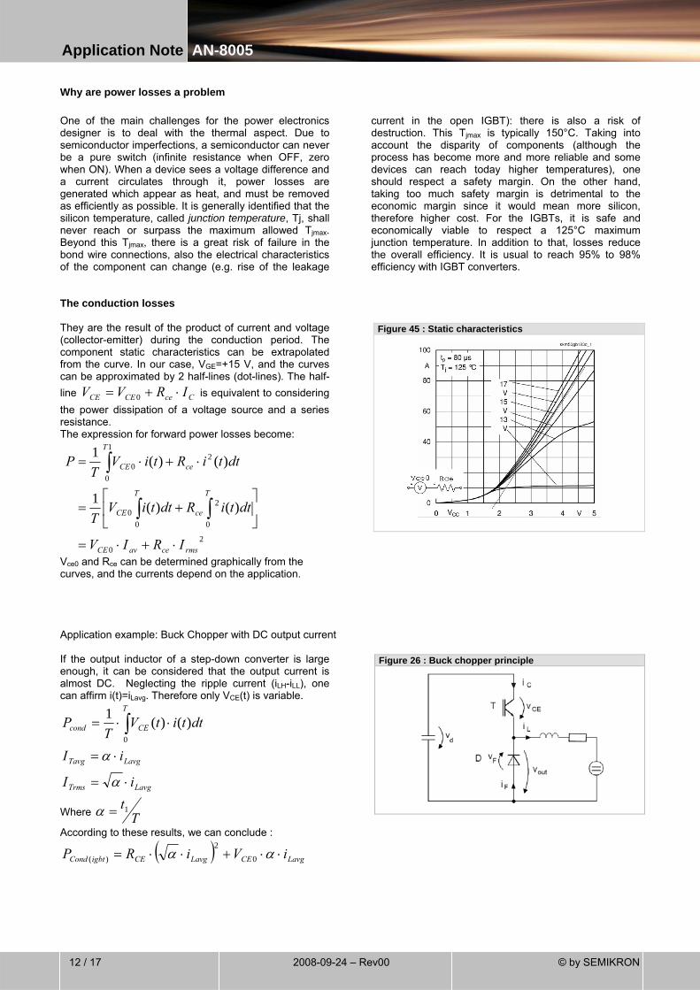
The conduction losses They are the result of the product of current and voltage (collector-emitter) during the conduction period. The component static characteristics can be extrapolated from the curve. In our case, VGE=+15 V, and the curves can be approximated by 2 half-lines (dot-lines). The half-line CceCECE IRVV ⋅+= 0 is equivalent to considering the power dissipation of a voltage source and a series resistance. The expression for forward power losses become:
20
0
2
00
1
0
20
)()(1
)()(1
rmsceavCE
T
ce
T
CE
T
ceCE
IRIV
dttiRdttiVT
dttiRtiVT
P
⋅+⋅=
⎥⎦
⎤⎢⎣
⎡+=
⋅+⋅=
∫∫
∫
Vce0 and Rce can be determined graphically from the curves, and the currents depend on the application. Application example: Buck Chopper with DC output current If the output inductor of a step-down converter is large enough, it can be considered that the output current is almost DC. Neglecting the ripple current (iLH-iLL), one can affirm i(t)=iLavg. Therefore only VCE(t) is variable.
LavgTrms
LavgTavg
T
CEcond
iI
iI
dttitVT
P
⋅=
⋅=
⋅⋅= ∫
α
α0
)()(1
Where Tt1=α
According to these results, we can conclude :
( ) LavgCELavgCEigbtCond iViRP ⋅⋅+⋅⋅= αα 0
2
)(
Figure 45 : Static characteristics
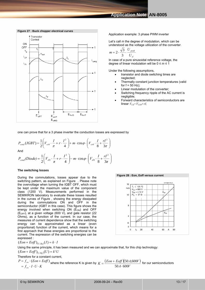
Figure 26 : Buck chopper principle
Application Note AN-8005
13 / 172008-09-24 – Rev00© by SEMIKRON
Figure 27 : Buck chopper electrical curves
Application example: 3 phase PWM inverter Let’s call m the degree of modulation, which can be understood as the voltage utilization of the converter.
d
peak
UU
m ⋅⋅=332
In case of a pure sinusoidal reference voltage, the degree of linear modulation will be 0 ≤ m ≤ 1 Under the following assumptions,
• transistor and diode switching times are neglected;
• Thermally constant junction temperatures (valid for f = 50 Hz);
• Linear modulation of the converter; • Switching frequency ripple of the AC current is
negligible; • Forward characteristics of semiconductors are
linear VCE=VCE0+rI,
one can prove that for a 3 phase inverter the conduction losses are expressed by
⎟⎟⎠
⎞⎜⎜⎝
⎛+⋅⋅⋅+⎟⎟
⎠
⎞⎜⎜⎝
⎛⋅+⋅=
πϕ
π 38cos
421)(
2
0
2
0rIIVmIrIVIGBTP cececond
And
⎟⎟⎠
⎞⎜⎜⎝
⎛+⋅⋅⋅−⎟⎟
⎠
⎞⎜⎜⎝
⎛⋅+⋅=
πrIIVmIr
πIV(Diode)P ddcond 38
cos42
1 2
0
2
0 ϕ
The switching losses During the commutations, losses appear due to the switching pattern, as explained on Figure . Please note the overvoltage when turning the IGBT OFF, which must be kept under the maximum value of the component class (1200 V). Measurements performed in the SEMIKRON laboratory to evaluate these losses resulted in the curves of Figure , showing the energy dissipated during the commutations ON and OFF in the semiconductor (IGBT in this case). This figure shows the energy involved when switching ON (EON) and OFF (EOFF), at a given voltage (600 V), and gate resistor (22 Ohms), as a function of the current. In our case, the measures of current dependence show that the switching energy can be approximated as a linear (even proportional) function of the current, which means for a first approach that these energies are proportional to the current. The expression of the switching energies can be expressed :
( ) IkIEoffEon RgU ⋅=+ )()( ,
Using the same principle, it has been measured and we can approximate that, for this chip technology:
( ) UkUEoffEon RgI ⋅=+ ')()( ,
Therefore for a constant current,
KUIfEoffEonfP
sw
sw
⋅⋅⋅=+⋅= )( where the reference K is given by ( )( )
VAVAEoffEonK
60050600,50
⋅+
= for our semiconductors
Figure 28 : Eon, Eoff versus current
Application Note AN-8005
14 / 17 2008-09-24 – Rev00 © by SEMIKRON
Application example: Buck Chopper with DC output current As expressed earlier, if we consider ILavg as constant,
KUIfEoffEonfP
Lavgsw
sw
⋅⋅⋅=+⋅= )(
Application example: 3 phase PWM inverer Based on the same principle, only the current varies in the previous expressions, replaced by the averaged commutated
value :
KUfI
P swrms
IGBTOFFON ⋅⋅⋅⋅
=+ π2
)(
From losses calculation to temperature estimation The losses must be dissipated to keep the component at a safe temperature. This is why a cooling device, or heat sink, is used. When a material is submitted to a heat transfer, we can define the thermal resistance between 2 points of this material as the ratio of the temperature rise between these 2 points and the heat power. This property can be seen as the equivalent of electrical resistance to the current. In thermal/electrical equivalence, • Temperature (K) voltage (V) • Power losses (W) current (A) • Thermal resistance (K/W) resistance (Ω) As for the electrical voltages, we will evaluate the temperature drops • ambient to heat sink, ΔTha • heat sink to case, ΔTch • case to junction. ΔTjc All the internal construction materials have a thermal resistance, and all interfaces between them add another thermal resistance. In order for it to be as small as possible, and therefore to improve the heat transfer from the chip to the heat sink and to the ambient, the following principles are used: • From the thermal perspective, all material interfaces
should be as thin as possible as the thermal resistance is proportional to the thickness of the material. The new SkiiP and MiniSKiiP products from SEMIKRON have addressed this problem by removing the 3 mm copper base plate and pressing the ceramic directly onto the heat sink.
• Thermal grease reduces the contact thermal resistance between the module and the heat sink, by filling the irregularities between both surfaces.
• The heat sink must be optimized: a large exchange surface with the ambient will improve the exchange coefficient with air. A bigger mass will have a greater capacitance for storing the heat, reducing the temperature ripples, but will have a higher gradient of temperature.
Figure 29 : internal construction of a power module
Application Note AN-8005
15 / 172008-09-24 – Rev00© by SEMIKRON
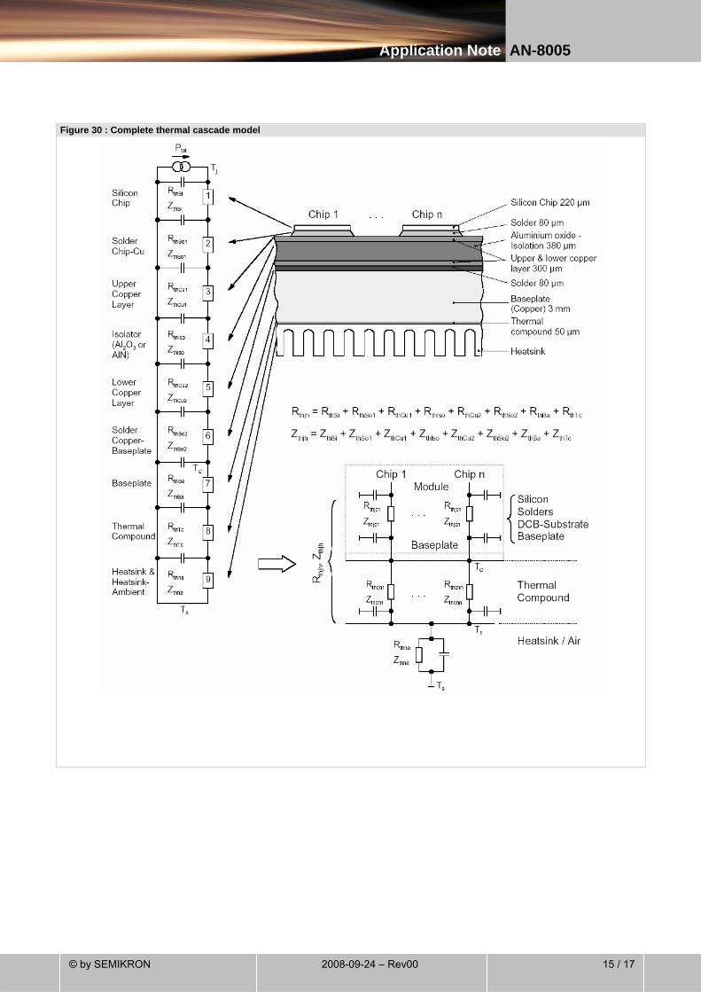
Figure 30 : Complete thermal cascade model
16 / 17 2008-09-24 – Rev00 © by SEMIKRON
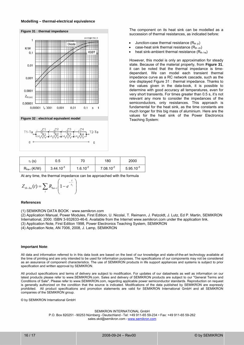
Modelling – thermal-electrical equivalence
The component on its heat sink can be modelled as a succession of thermal resistances, as indicated before: • Junction-case thermal resistance (Rth jc) • case-heat sink thermal resistance (Rth ch) • heat sink-ambient thermal resistance (Rth ha) However, this model is only an approximation for steady state. Because of the material property, from Figure 31, it can be noted that the thermal impedance is time-dependant. We can model each transient thermal impedance curve as a RC network cascade, such as the one displayed Figure 31 : thermal impedance. Thanks to the values given in the data-book, it is possible to determine with good accuracy all temperatures, even for very short transients. For times greater than 0.5 s, it’s not relevant any more to consider the impedances of the semiconductors, only resistances. This approach is fundamental for the heat sink, as the time constants are much longer for this big mass of aluminium. Here are the values for the heat sink of the Power Electronics Teaching System:
At any time, the thermal impedance can be approached with the formula
∑ ⎟⎟⎠
⎞⎜⎜⎝
⎛−=
−
−−i
t
ihahathieRtZ τ1)(
References (1) SEMIKRON DATA BOOK : www.semikron.com (2) Application Manual, Power Modules, First Edition, U. Nicolaï, T. Reimann, J. Petzoldt, J. Lutz, Ed P. Martin, SEMIKRON International, 2000. ISBN 3-932633-46-6. Available from the Internet www.semikron.com under the application link. (3) Application Note, First Edition 1998, Power Electronics Teaching System, SEMIKRON (4) Application Note, AN 7006, 2008, J. Lamp, SEMIKRON Important Note: All data and information referred to in this data book are based on the best of our knowledge and state-of-the-art technology available at the time of printing and are only intended to be used for information purposes. The specifications of our components may not be considered as an assurance of component characteristics. The use of SEMIKRON products in life support appliances and systems is subject to prior specification and written approval by SEMIKRON. All product specifications and terms of delivery are subject to modification. For updates of our datasheets as well as information on our latest products please refer to www.SEMIKRON.com. Sales and delivery of SEMIKRON products are subject to our "General Terms and Conditions of Sale". Please refer to www.SEMIKRON.com, regarding applicable power semiconductor standards. Reproduction on request is generally authorized on the condition that the source is indicated. Modifications of the data published by SEMIKRON are expressly prohibited. All product specifications and promotion statements are valid for SEMIKRON International GmbH and all SEMIKRON companies of the SEMIKRON group. © by SEMIKRON International GmbH
SEMIKRON INTERNATIONAL GmbH P.O. Box 820251 • 90253 Nürnberg • Deutschland • Tel: +49 911-65 59-234 • Fax: +49 911-65 59-262
[email protected] • www.semikron.com
Figure 31 : thermal impedance
Figure 32 : electrical equivalent model
τI (s) 0.5 70 180 2000
Rha-i (K/W) 3.44.10-3 1.6.10-2 7.08.10-2 5.95.10-3
Application Note AN-8005
17 / 172008-09-24 – Rev00© by SEMIKRON
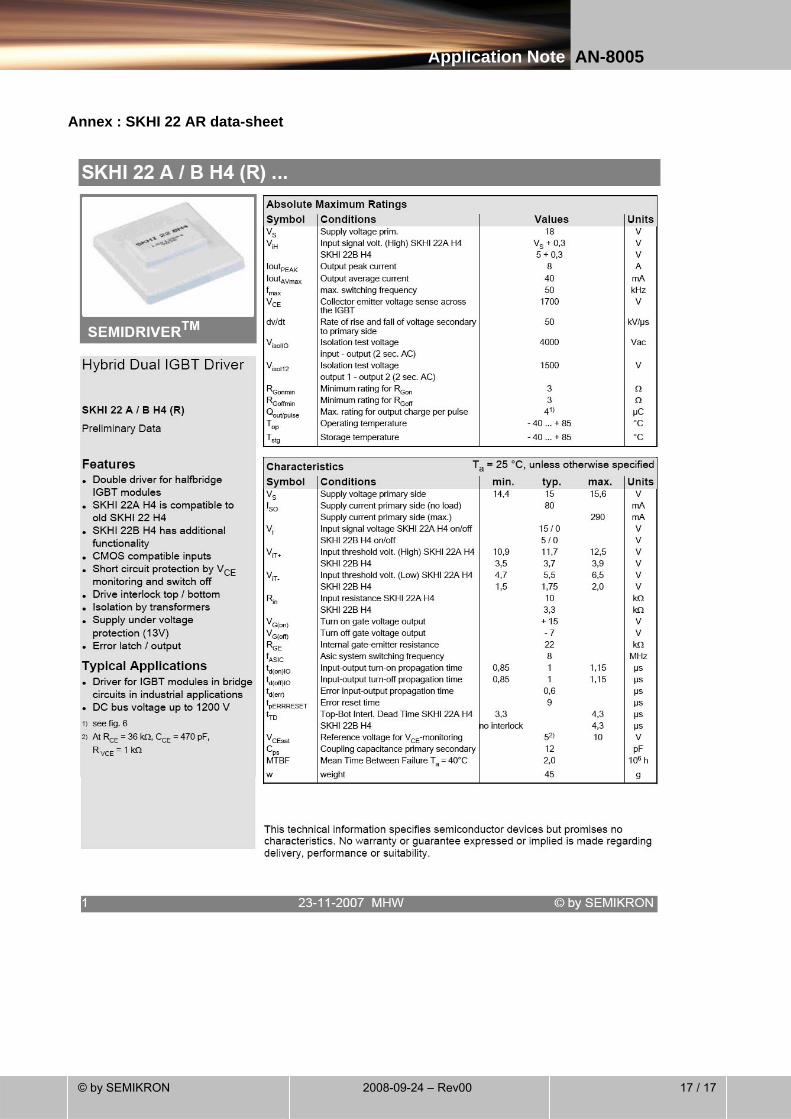
Annex : SKHI 22 AR data-sheet