any-frequency precision clocks si5316, … · si53xx-rm rev. 1.3 5 6.8. frame synchronization...
TRANSCRIPT

Rev. 1.3 10/16 Copyright © 2016 by Silicon Laboratories Si53xx-RM
ANY-FREQUENCY PRECISION CLOCKSSi5316, Si5319, Si5322, Si5323, Si5324, Si5325,Si5326, Si5327, Si5328, Si5365, Si5366, Si5367,
Si5368, Si5369, Si5374, Si5375, Si5376FAMILY REFERENCE MANUAL

Si53xx-RM
2 Rev. 1.3

Si53xx-RM
Rev. 1.3 3
TABLE OF CONTENTS
Section Page1. Any-Frequency Precision Clock Product Family Overview . . . . . . . . . . . . . . . . . . . . . .122. Wideband Devices . . . . . . . . . . . . . . . . . . . . . . . . . . . . . . . . . . . . . . . . . . . . . . . . . . . . . . .15
2.1. Narrowband vs. Wideband Overview . . . . . . . . . . . . . . . . . . . . . . . . . . . . . . . . . . . .153. Any-Frequency Clock Family Members . . . . . . . . . . . . . . . . . . . . . . . . . . . . . . . . . . . . . .16
3.1. Si5316 . . . . . . . . . . . . . . . . . . . . . . . . . . . . . . . . . . . . . . . . . . . . . . . . . . . . . . . . . . . .163.2. Si5319 . . . . . . . . . . . . . . . . . . . . . . . . . . . . . . . . . . . . . . . . . . . . . . . . . . . . . . . . . . . .173.3. Si5322 . . . . . . . . . . . . . . . . . . . . . . . . . . . . . . . . . . . . . . . . . . . . . . . . . . . . . . . . . . . .183.4. Si5323 . . . . . . . . . . . . . . . . . . . . . . . . . . . . . . . . . . . . . . . . . . . . . . . . . . . . . . . . . . . .193.5. Si5324 . . . . . . . . . . . . . . . . . . . . . . . . . . . . . . . . . . . . . . . . . . . . . . . . . . . . . . . . . . . .203.6. Si5325 . . . . . . . . . . . . . . . . . . . . . . . . . . . . . . . . . . . . . . . . . . . . . . . . . . . . . . . . . . . .213.7. Si5326 . . . . . . . . . . . . . . . . . . . . . . . . . . . . . . . . . . . . . . . . . . . . . . . . . . . . . . . . . . . .223.8. Si5327 . . . . . . . . . . . . . . . . . . . . . . . . . . . . . . . . . . . . . . . . . . . . . . . . . . . . . . . . . . . .233.9. Si5328 . . . . . . . . . . . . . . . . . . . . . . . . . . . . . . . . . . . . . . . . . . . . . . . . . . . . . . . . . . . .243.10. Si5365 . . . . . . . . . . . . . . . . . . . . . . . . . . . . . . . . . . . . . . . . . . . . . . . . . . . . . . . . . . .253.11. Si5366 . . . . . . . . . . . . . . . . . . . . . . . . . . . . . . . . . . . . . . . . . . . . . . . . . . . . . . . . . . .263.12. Si5367 . . . . . . . . . . . . . . . . . . . . . . . . . . . . . . . . . . . . . . . . . . . . . . . . . . . . . . . . . . .273.13. Si5368 . . . . . . . . . . . . . . . . . . . . . . . . . . . . . . . . . . . . . . . . . . . . . . . . . . . . . . . . . . .283.14. Si5369 . . . . . . . . . . . . . . . . . . . . . . . . . . . . . . . . . . . . . . . . . . . . . . . . . . . . . . . . . . .293.15. Si5374/75/76 Compared to Si5324/19/26 . . . . . . . . . . . . . . . . . . . . . . . . . . . . . . . .293.16. Si5374 . . . . . . . . . . . . . . . . . . . . . . . . . . . . . . . . . . . . . . . . . . . . . . . . . . . . . . . . . . .303.17. Si5375 . . . . . . . . . . . . . . . . . . . . . . . . . . . . . . . . . . . . . . . . . . . . . . . . . . . . . . . . . . .313.18. Si5376 . . . . . . . . . . . . . . . . . . . . . . . . . . . . . . . . . . . . . . . . . . . . . . . . . . . . . . . . . . .32
4. DSPLL (All Devices) . . . . . . . . . . . . . . . . . . . . . . . . . . . . . . . . . . . . . . . . . . . . . . . . . . . . . .334.1. Clock Multiplication . . . . . . . . . . . . . . . . . . . . . . . . . . . . . . . . . . . . . . . . . . . . . . . . . .344.2. PLL Performance . . . . . . . . . . . . . . . . . . . . . . . . . . . . . . . . . . . . . . . . . . . . . . . . . . .35
4.2.1. Jitter Generation . . . . . . . . . . . . . . . . . . . . . . . . . . . . . . . . . . . . . . . . . . . . . . . . . . . . . . . . . . . . 354.2.2. Jitter Transfer. . . . . . . . . . . . . . . . . . . . . . . . . . . . . . . . . . . . . . . . . . . . . . . . . . . . . . . . . . . . . . . 354.2.3. Jitter Tolerance . . . . . . . . . . . . . . . . . . . . . . . . . . . . . . . . . . . . . . . . . . . . . . . . . . . . . . . . . . . . . 36
5. Pin Control Parts (Si5316, Si5322, Si5323, Si5365, Si5366) . . . . . . . . . . . . . . . . . . . . . .375.1. Clock Multiplication (Si5316, Si5322, Si5323, Si5365, Si5366) . . . . . . . . . . . . . . . .37
5.1.1. Clock Multiplication (Si5316) . . . . . . . . . . . . . . . . . . . . . . . . . . . . . . . . . . . . . . . . . . . . . . . . . . . 375.1.2. Clock Multiplication (Si5322, Si5323, Si5365, Si5366) . . . . . . . . . . . . . . . . . . . . . . . . . . . . . . . 395.1.3. CKOUT3 and CKOUT4 (Si5365 and Si5366) . . . . . . . . . . . . . . . . . . . . . . . . . . . . . . . . . . . . . . 515.1.4. Loop bandwidth (Si5316, Si5322, Si5323, Si5365, Si5366) . . . . . . . . . . . . . . . . . . . . . . . . . . . 515.1.5. Jitter Tolerance (Si5316, Si5323, Si5366) . . . . . . . . . . . . . . . . . . . . . . . . . . . . . . . . . . . . . . . . . 515.1.6. Narrowband Performance (Si5316, Si5323, Si5366). . . . . . . . . . . . . . . . . . . . . . . . . . . . . . . . . 515.1.7. Input-to-Output Skew (Si5316, Si5323, Si5366) . . . . . . . . . . . . . . . . . . . . . . . . . . . . . . . . . . . . 515.1.8. Wideband Performance (Si5322 and Si5365) . . . . . . . . . . . . . . . . . . . . . . . . . . . . . . . . . . . . . . 515.1.9. Lock Detect (Si5322 and Si5365) . . . . . . . . . . . . . . . . . . . . . . . . . . . . . . . . . . . . . . . . . . . . . . . 515.1.10. Input-to-Output Skew (Si5322 and Si5365) . . . . . . . . . . . . . . . . . . . . . . . . . . . . . . . . . . . . . . . 51
5.2. PLL Self-Calibration . . . . . . . . . . . . . . . . . . . . . . . . . . . . . . . . . . . . . . . . . . . . . . . . .525.2.1. Input Clock Stability during Internal Self-Calibration (Si5316, Si5322, Si5323, Si5365, Si5366). . . . . . . . . . . . . . . . . . . . . . . . . . . . . . . . . . . . . . . . . . . . . . 525.2.2. Self-Calibration caused by Changes in Input Frequency (Si5316, Si5322, Si5323, Si5365, Si5366). . . . . . . . . . . . . . . . . . . . . . . . . . . . . . . . . . . . . . . . . . . . . . 52

Si53xx-RM
4 Rev. 1.3
5.2.3. Recommended Reset Guidelines (Si5316, Si5322, Si5323, Si5365, Si5366). . . . . . . . . . . . . . 525.3. Pin Control Input Clock Control . . . . . . . . . . . . . . . . . . . . . . . . . . . . . . . . . . . . . . . . .54
5.3.1. Manual Clock Selection . . . . . . . . . . . . . . . . . . . . . . . . . . . . . . . . . . . . . . . . . . . . . . . . . . . . . . . 545.3.2. Automatic Clock Selection (Si5322, Si5323, Si5365, Si5366) . . . . . . . . . . . . . . . . . . . . . . . . . . 555.3.3. Hitless Switching with Phase Build-Out (Si5323, Si5366) . . . . . . . . . . . . . . . . . . . . . . . . . . . . . 56
5.4. Digital Hold/VCO Freeze . . . . . . . . . . . . . . . . . . . . . . . . . . . . . . . . . . . . . . . . . . . . . .575.4.1. Narrowband Digital Hold (Si5316, Si5323, Si5366) . . . . . . . . . . . . . . . . . . . . . . . . . . . . . . . . . . 575.4.2. Recovery from Digital Hold (Si5316, Si5323, Si5366) . . . . . . . . . . . . . . . . . . . . . . . . . . . . . . . . 575.4.3. Wideband VCO Freeze (Si5322, Si5365) . . . . . . . . . . . . . . . . . . . . . . . . . . . . . . . . . . . . . . . . . 57
5.5. Frame Synchronization (Si5366) . . . . . . . . . . . . . . . . . . . . . . . . . . . . . . . . . . . . . . . .575.6. Output Phase Adjust (Si5323, Si5366) . . . . . . . . . . . . . . . . . . . . . . . . . . . . . . . . . . .58
5.6.1. FSYNC Realignment (Si5366) . . . . . . . . . . . . . . . . . . . . . . . . . . . . . . . . . . . . . . . . . . . . . . . . . . 585.6.2. Including FSYNC Inputs in Clock Selection (Si5366) . . . . . . . . . . . . . . . . . . . . . . . . . . . . . . . . 585.6.3. FS_OUT Polarity and Pulse Width Control (Si5366) . . . . . . . . . . . . . . . . . . . . . . . . . . . . . . . . . 585.6.4. Using FS_OUT as a Fifth Output Clock (Si5366) . . . . . . . . . . . . . . . . . . . . . . . . . . . . . . . . . . . 585.6.5. Disabling FS_OUT (Si5366) . . . . . . . . . . . . . . . . . . . . . . . . . . . . . . . . . . . . . . . . . . . . . . . . . . . 59
5.7. Output Clock Drivers . . . . . . . . . . . . . . . . . . . . . . . . . . . . . . . . . . . . . . . . . . . . . . . . .595.7.1. LVPECL and CMOS TQFP Output Signal Format Restrictions at 3.3 V (Si5365, Si5366) . . . . 59
5.8. PLL Bypass Mode . . . . . . . . . . . . . . . . . . . . . . . . . . . . . . . . . . . . . . . . . . . . . . . . . . .605.9. Alarms . . . . . . . . . . . . . . . . . . . . . . . . . . . . . . . . . . . . . . . . . . . . . . . . . . . . . . . . . . . .60
5.9.1. Loss-of-Signal Alarms (Si5316, Si5322, Si5323, Si5365, Si5366) . . . . . . . . . . . . . . . . . . . . . . 605.9.2. FOS Alarms (Si5365 and Si5366) . . . . . . . . . . . . . . . . . . . . . . . . . . . . . . . . . . . . . . . . . . . . . . . 605.9.3. FSYNC Align Alarm (Si5366 and CK_CONF = 1 and FRQTBL = L) . . . . . . . . . . . . . . . . . . . . . 615.9.4. C1B and C2B Alarm Outputs (Si5316, Si5322, Si5323) . . . . . . . . . . . . . . . . . . . . . . . . . . . . . . 615.9.5. C1B, C2B, C3B, and ALRMOUT Outputs (Si5365, Si5366) . . . . . . . . . . . . . . . . . . . . . . . . . . . 61
5.10. Device Reset . . . . . . . . . . . . . . . . . . . . . . . . . . . . . . . . . . . . . . . . . . . . . . . . . . . . . .625.11. DSPLLsim Configuration Software . . . . . . . . . . . . . . . . . . . . . . . . . . . . . . . . . . . . .62
6. Microprocessor Controlled Parts (Si5319, Si5324, Si5325, Si5326, Si5327, Si5328, Si5367, Si5368, Si5369, Si5374, Si5375, and Si5376) . . . . . . . . . . . . . . . . . . . . . . . . . . . .63
6.1. Clock Multiplication . . . . . . . . . . . . . . . . . . . . . . . . . . . . . . . . . . . . . . . . . . . . . . . . . .636.1.1. Jitter Tolerance (Si5319, Si5324, Si5325, Si5326, Si5327, Si5328, Si5368, Si5369, Si5374, Si5375, and Si5376) . . . . . . . . . . . . . . . . . . . . . . . . . . . . . 636.1.2. Wideband Parts (Si5325, Si5367) . . . . . . . . . . . . . . . . . . . . . . . . . . . . . . . . . . . . . . . . . . . . . . . 636.1.3. Narrowband Parts (Si5319, Si5324, Si5326, Si5327, Si5328, Si5368, Si5369, Si5374, Si5375, and Si5376) . . . . . . . . . . . . . . . . . . . . . . . . . . . . . 646.1.4. Loop Bandwidth (Si5319, Si5326, Si5368, Si5375, and Si5376). . . . . . . . . . . . . . . . . . . . . . . . 666.1.5. Lock Detect (Si5319, Si5326, Si5327, Si5328, Si5368, Si5369, Si5374, Si5375, and Si5376) . . . . . . . . . . . . . . . . . . . . . . . . . . . . . . . . . . . . . . . . . . . . . . . . . 66
6.2. PLL Self-Calibration . . . . . . . . . . . . . . . . . . . . . . . . . . . . . . . . . . . . . . . . . . . . . . . . .666.2.1. Initiating Internal Self-Calibration . . . . . . . . . . . . . . . . . . . . . . . . . . . . . . . . . . . . . . . . . . . . . . . . 676.2.2. Input Clock Stability during Internal Self-Calibration . . . . . . . . . . . . . . . . . . . . . . . . . . . . . . . . . 676.2.3. Self-Calibration Caused by Changes in Input Frequency . . . . . . . . . . . . . . . . . . . . . . . . . . . . . 676.2.4. Narrowband Input-to-Output Skew (Si5319, Si5324, Si5326, Si5327, Si5328, Si5368, Si5369, Si5374, Si5375, and Si5376) . . . . . . . . . . . . . . . . . . . . . . . . . . . . . . . . . . . . 676.2.5. Clock Output Behavior Before and During ICAL (Si5319, Si5324, Si5326, Si5327, Si5328, Si5368, Si5369, Si5374, Si5375, and Si5376) . . . . . . . . . . . . . . . . . . . . . . . . . . . . . 68
6.3. Input Clock Configurations (Si5367 and Si5368) . . . . . . . . . . . . . . . . . . . . . . . . . . .696.4. Input Clock Control . . . . . . . . . . . . . . . . . . . . . . . . . . . . . . . . . . . . . . . . . . . . . . . . . .69
6.4.1. Manual Clock Selection (Si5324, Si5325, Si5326, Si5328, Si5367, Si5368, Si5369, Si5374, and Si5376). . . . . . . . . . . . . . . . . . . . . . . . . . . . . . . . . . . . . . . . . . . 706.4.2. Automatic Clock Selection (Si5324, Si5325, Si5326, Si5328, Si5367, Si5368, Si5369, Si5374, and Si5376). . . . . . . . . . . . . . . . . . . . . . . . . . . . . . . . . . . . . . . . . . . 71

Si53xx-RM
Rev. 1.3 5
6.4.3. Hitless Switching with Phase Build-Out (Si5324, Si5326, Si5327, Si5328, Si5368, Si5369, Si5374, and Si5376). . . . . . . . . . . . . . . . . . . . . . . . . . . . . . . . . . . . . . . . . . . 72
6.5. Si5319, Si5324, Si5326, Si5327, Si5328, Si5368, Si5369, Si5374, Si5375, and Si5376 Free Run Mode . . . . . . . . . . . . . . . . . . . . . . . .736.5.1. Free Run Mode Programming Procedure . . . . . . . . . . . . . . . . . . . . . . . . . . . . . . . . . . . . . . . . . 736.5.2. Clock Control Logic in Free Run Mode . . . . . . . . . . . . . . . . . . . . . . . . . . . . . . . . . . . . . . . . . . . 736.5.3. Free Run Reference Frequency Constraints . . . . . . . . . . . . . . . . . . . . . . . . . . . . . . . . . . . . . . . 746.5.4. Free Run Reference Frequency Constraints . . . . . . . . . . . . . . . . . . . . . . . . . . . . . . . . . . . . . . . 74
6.6. Digital Hold . . . . . . . . . . . . . . . . . . . . . . . . . . . . . . . . . . . . . . . . . . . . . . . . . . . . . . . .756.6.1. Narrowband Digital Hold (Si5316, Si5324, Si5326, Si5328, Si5368, Si5369, Si5374, Si5376) . . . . . . . . . . . . . . . . . . . . . . . . . . . . . . . . . . . . . . . . . . . . . . . . . . . . . 756.6.2. History Settings for Low Bandwidth Devices (Si5324, Si5327, Si5328, Si5369, Si5374) . . . . . 776.6.3. Recovery from Digital Hold (Si5319, Si5324, Si5326, Si5327, Si5328, Si5368, Si5369, Si5374, and Si5376) . . . . . . . . . . . . . . . . . . . . . . . . . . . . . . . . . . . . . . . . . . . . . . . . . 776.6.4. VCO Freeze (Si5319, Si5325, Si5367, Si5375). . . . . . . . . . . . . . . . . . . . . . . . . . . . . . . . . . . . . 776.6.5. Digital Hold versus VCO Freeze . . . . . . . . . . . . . . . . . . . . . . . . . . . . . . . . . . . . . . . . . . . . . . . . 77
6.7. Output Phase Adjust (Si5326, Si5368) . . . . . . . . . . . . . . . . . . . . . . . . . . . . . . . . . . .786.7.1. Coarse Skew Control (Si5326, Si5368) . . . . . . . . . . . . . . . . . . . . . . . . . . . . . . . . . . . . . . . . . . . 786.7.2. Fine Skew Control (Si5326, Si5368) . . . . . . . . . . . . . . . . . . . . . . . . . . . . . . . . . . . . . . . . . . . . . 786.7.3. Independent Skew (Si5324, Si5326, Si5328, Si5368, Si5369, Si5374, and Si5376) . . . . . . . . 796.7.4. Output-to-output Skew (Si5324, Si5326, Si5327, Si5328, Si5368, Si5369, Si5374, and Si5376) . . . . . . . . . . . . . . . . . . . . . . . . . . . . . . . . . . . . . . . . . . . . . . . . . 796.7.5. Input-to-Output Skew (All Devices) . . . . . . . . . . . . . . . . . . . . . . . . . . . . . . . . . . . . . . . . . . . . . . 79
6.8. Frame Synchronization Realignment (Si5368 and CK_CONFIG_REG = 1) . . . . . . .796.8.1. FSYNC Realignment (Si5368) . . . . . . . . . . . . . . . . . . . . . . . . . . . . . . . . . . . . . . . . . . . . . . . . . . 816.8.2. FSYNC Skew Control (Si5368) . . . . . . . . . . . . . . . . . . . . . . . . . . . . . . . . . . . . . . . . . . . . . . . . . 826.8.3. Including FSYNC Inputs in Clock Selection (Si5368) . . . . . . . . . . . . . . . . . . . . . . . . . . . . . . . . 826.8.4. FS_OUT Polarity and Pulse Width Control (Si5368) . . . . . . . . . . . . . . . . . . . . . . . . . . . . . . . . . 826.8.5. Using FS_OUT as a Fifth Output Clock (Si5368) . . . . . . . . . . . . . . . . . . . . . . . . . . . . . . . . . . . 82
6.9. Output Clock Drivers (Si5319, Si5324, Si5325, Si5326, Si5327, Si5328, Si5367, Si5368, Si5369, Si5374, Si5375, Si5376) . . . . . . . . . . . . . . . . . . . . . . . . . . . . . . . . .836.9.1. Disabling CKOUTn. . . . . . . . . . . . . . . . . . . . . . . . . . . . . . . . . . . . . . . . . . . . . . . . . . . . . . . . . . . 836.9.2. LVPECL TQFP Output Signal Format Restrictions at 3.3 V (Si5367, Si5368, Si5369) . . . . . . . 83
6.10. PLL Bypass Mode (Si5319, Si5324, Si5325, Si5326, Si5327, Si5328, Si5367, Si5368, Si5369, Si5374, Si5375, and Si5376) . . . . . . . . .84
6.11. Alarms (Si5319, Si5324, Si5325, Si5326, Si5327, Si5328, Si5367, Si5368, Si5369, Si5374, Si5375, and Si5376) . . . . . . . . . . . . . . . . . . . . . . .846.11.1. Loss-of-Signal Alarms (Si5319, Si5324, Si5325, Si5326, Si5327, Si5328, Si5367, Si5368, Si5369, Si5374, Si5375, and Si5376) . . . . . . . . . . . . . . . . . . . . . . . 846.11.2. FOS Algorithm (Si5324, Si5325, Si5326, Si5328, Si5368, Si5369, Si5374, and Si5376) . . . . 856.11.3. C1B, C2B (Si5319, Si5324, Si5325, Si5326, Si5327, Si5328, Si5374, Si5375, and Si5376) . . . . . . . . . . . . . . . . . . . . . . . . . . . . . . . . . . . . . . . . . . . . . . . . . 876.11.4. LOS (Si5319, Si5375) . . . . . . . . . . . . . . . . . . . . . . . . . . . . . . . . . . . . . . . . . . . . . . . . . . . . . . . 876.11.5. C1B, C2B, C3B, ALRMOUT (Si5367, Si5368, Si5369 [CK_CONFIG_REG = 0]) . . . . . . . . . . 876.11.6. C1B, C2B, C3B, ALRMOUT (Si5368 [CK_CONFIG_REG = 1]) . . . . . . . . . . . . . . . . . . . . . . . 886.11.7. LOS Algorithm for Reference Clock Input (Si5319, Si5324, Si5326, Si5327, Si5328, Si5368, Si5369, Si5374, Si5375, and Si5376) . . . . . . . . . . . . . . . . . . . . . . . 896.11.8. LOL (Si5319, Si5324, Si5326, Si5327, Si5328, Si5368, Si5369, Si5374, Si5375, and Si5376) . . . . . . . . . . . . . . . . . . . . . . . . . . . . . . . . . . . . . . . . . . . . . . . . . . . . . . . . 896.11.9. Device Interrupts . . . . . . . . . . . . . . . . . . . . . . . . . . . . . . . . . . . . . . . . . . . . . . . . . . . . . . . . . . . 89
6.12. Device Reset . . . . . . . . . . . . . . . . . . . . . . . . . . . . . . . . . . . . . . . . . . . . . . . . . . . . . .89

Si53xx-RM
6 Rev. 1.3
6.13. I2C Serial Microprocessor Interface . . . . . . . . . . . . . . . . . . . . . . . . . . . . . . . . . . . .906.14. Serial Microprocessor Interface (SPI) . . . . . . . . . . . . . . . . . . . . . . . . . . . . . . . . . . .91
6.14.1. Default Device Configuration . . . . . . . . . . . . . . . . . . . . . . . . . . . . . . . . . . . . . . . . . . . . . . . . . . 936.15. Register Descriptions . . . . . . . . . . . . . . . . . . . . . . . . . . . . . . . . . . . . . . . . . . . . . . .936.16. DSPLLsim Configuration Software . . . . . . . . . . . . . . . . . . . . . . . . . . . . . . . . . . . . .93
7. High-Speed I/O . . . . . . . . . . . . . . . . . . . . . . . . . . . . . . . . . . . . . . . . . . . . . . . . . . . . . . . . . .947.1. Input Clock Buffers . . . . . . . . . . . . . . . . . . . . . . . . . . . . . . . . . . . . . . . . . . . . . . . . . .947.2. Output Clock Drivers . . . . . . . . . . . . . . . . . . . . . . . . . . . . . . . . . . . . . . . . . . . . . . . . .96
7.2.1. LVPECL TQFP Output Signal Format Restrictions at 3.3 V (Si5367, Si5368, Si5369) . . . . . . . 967.2.2. Typical Output Circuits. . . . . . . . . . . . . . . . . . . . . . . . . . . . . . . . . . . . . . . . . . . . . . . . . . . . . . . . 967.2.3. Typical Clock Output Scope Shots . . . . . . . . . . . . . . . . . . . . . . . . . . . . . . . . . . . . . . . . . . . . . . 98
7.3. Typical Scope Shots for SFOUT Options . . . . . . . . . . . . . . . . . . . . . . . . . . . . . . . . .997.4. Crystal/Reference Clock Interfaces (Si5316, Si5319, Si5323, Si5324,
Si5326, Si5327, Si5328, Si5366, Si5368, Si5369, Si5374, Si5375, and Si5376) . .1027.5. Three-Level (3L) Input Pins (No External Resistors) . . . . . . . . . . . . . . . . . . . . . . .1047.6. Three-Level (3L) Input Pins (With External Resistors) . . . . . . . . . . . . . . . . . . . . . .105
8. Power Supply . . . . . . . . . . . . . . . . . . . . . . . . . . . . . . . . . . . . . . . . . . . . . . . . . . . . . . . . . .1069. Packages and Ordering Guide . . . . . . . . . . . . . . . . . . . . . . . . . . . . . . . . . . . . . . . . . . . .107Appendix A—Narrowband References . . . . . . . . . . . . . . . . . . . . . . . . . . . . . . . . . . . . . . .108Appendix B—Frequency Plans and Typical Jitter Performance (Si5316, Si5319, Si5323, Si5324, Si5326, Si5327, Si5366, Si5368, Si5369, Si5374, Si5375, and Si5376) . . . . . . . .112Appendix C—Typical Phase Noise Plots . . . . . . . . . . . . . . . . . . . . . . . . . . . . . . . . . . . . . .119Appendix D—Alarm Structure . . . . . . . . . . . . . . . . . . . . . . . . . . . . . . . . . . . . . . . . . . . . . . .137Appendix E—Internal Pullup, Pulldown by Pin . . . . . . . . . . . . . . . . . . . . . . . . . . . . . . . . .140Appendix F—Typical Performance: Bypass Mode, PSRR, Crosstalk, Output Format Jitter . . . . . . . . . . . . . . . . . . . . . . . . . . . . . . . . . . . . . . . . . . . . .147Appendix G—Near Integer Ratios . . . . . . . . . . . . . . . . . . . . . . . . . . . . . . . . . . . . . . . . . . . .155Appendix H—Jitter Attenuation and Loop BW . . . . . . . . . . . . . . . . . . . . . . . . . . . . . . . . .157Appendix I—Response to a Frequency Step Function . . . . . . . . . . . . . . . . . . . . . . . . . . .162Appendix J—Si5374, Si5375, Si5376 PCB Layout Recommendations . . . . . . . . . . . . . .163Appendix K—Si5374, Si5375, and Si5376 Crosstalk . . . . . . . . . . . . . . . . . . . . . . . . . . . . .167Appendix L—Jitter Transfer and Peaking . . . . . . . . . . . . . . . . . . . . . . . . . . . . . . . . . . . . .174Document Change List . . . . . . . . . . . . . . . . . . . . . . . . . . . . . . . . . . . . . . . . . . . . . . . . . . . .177Contact Information . . . . . . . . . . . . . . . . . . . . . . . . . . . . . . . . . . . . . . . . . . . . . . . . . . . . . . .178

Si53xx-RM
Rev. 1.3 7
LIST OF FIGURES
Figure 1. Si5316 Any-Frequency Jitter Attenuator Block Diagram . . . . . . . . . . . . . . . . . . . . . 16Figure 2. Si5319 Any-Frequency Jitter Attenuating Clock Multiplier Block Diagram . . . . . . . .17Figure 3. Si5322 Low Jitter Clock Multiplier Block Diagram . . . . . . . . . . . . . . . . . . . . . . . . . . 18Figure 4. Si5323 Jitter Attenuating Clock Multiplier Block Diagram . . . . . . . . . . . . . . . . . . . . 19Figure 5. Si5324 Clock Multiplier and Jitter Attenuator Block Diagram. . . . . . . . . . . . . . . . . . 20Figure 6. Si5325 Low Jitter Clock Multiplier Block Diagram . . . . . . . . . . . . . . . . . . . . . . . . . . 21Figure 7. Si5326 Clock Multiplier and Jitter Attenuator Block Diagram. . . . . . . . . . . . . . . . . . 22Figure 8. Si5327 Clock Multiplier and Jitter Attenuator Block Diagram. . . . . . . . . . . . . . . . . . 23Figure 9. Si5328 Clock Multiplier and Jitter Attenuator Block Diagram. . . . . . . . . . . . . . . . . . 24Figure 10. Si5365 Low Jitter Clock Multiplier Block Diagram . . . . . . . . . . . . . . . . . . . . . . . . . 25Figure 11. Si5366 Jitter Attenuating Clock Multiplier Block Diagram . . . . . . . . . . . . . . . . . . . 26Figure 12. Si5367 Clock Multiplier Block Diagram . . . . . . . . . . . . . . . . . . . . . . . . . . . . . . . . . 27Figure 13. Si5368 Clock Multiplier and Jitter Attenuator Block Diagram. . . . . . . . . . . . . . . . . 28Figure 14. Si5369 Clock Multiplier and Jitter Attenuator Block Diagram. . . . . . . . . . . . . . . . . 29Figure 15. Si5374 Functional Block Diagram . . . . . . . . . . . . . . . . . . . . . . . . . . . . . . . . . . . . . 30Figure 16. Si5375 Functional Block Diagram . . . . . . . . . . . . . . . . . . . . . . . . . . . . . . . . . . . . . 31Figure 17. Si5376 Functional Block Diagram . . . . . . . . . . . . . . . . . . . . . . . . . . . . . . . . . . . . . 32Figure 18. Any-Frequency Precision Clock DSPLL Block Diagram . . . . . . . . . . . . . . . . . . . . 33Figure 19. Clock Multiplication Circuit . . . . . . . . . . . . . . . . . . . . . . . . . . . . . . . . . . . . . . . . . . . 34Figure 20. PLL Jitter Transfer Mask/Template . . . . . . . . . . . . . . . . . . . . . . . . . . . . . . . . . . . . 35Figure 21. Jitter Tolerance Mask/Template. . . . . . . . . . . . . . . . . . . . . . . . . . . . . . . . . . . . . . . 36Figure 22. Si5316 Divisor Ratios. . . . . . . . . . . . . . . . . . . . . . . . . . . . . . . . . . . . . . . . . . . . . . . 38Figure 23. Wideband PLL Divider Settings (Si5325, Si5367) . . . . . . . . . . . . . . . . . . . . . . . . . 63Figure 24. Narrowband PLL Divider Settings (Si5319, Si5324, Si5326, Si5327, Si5328, Si5368, Si5369, Si5374, Si5375, and Si5376) . . . . . . . . . . . . . . . . . . . . . . . 65Figure 25. Si5324, Si5325, Si5326, Si5327, Si5328, Si5374, and Si5376 Input Clock Selection . . . . . . . . . . . . . . . . . . . . . . . . . . . . . . . . . . . . . . . . . . . . . . 69Figure 26. Si5367, Si5368, and Si5369 Input Clock Selection . . . . . . . . . . . . . . . . . . . . . . . . 70Figure 27. Free Run Mode Block Diagram . . . . . . . . . . . . . . . . . . . . . . . . . . . . . . . . . . . . . . . .73Figure 28. Parameters in History Value of M . . . . . . . . . . . . . . . . . . . . . . . . . . . . . . . . . . . . . 75Figure 29. Digital Hold vs. VCO Freeze Example . . . . . . . . . . . . . . . . . . . . . . . . . . . . . . . . . . 77Figure 30. Frame Sync Frequencies . . . . . . . . . . . . . . . . . . . . . . . . . . . . . . . . . . . . . . . . . . . . 80Figure 31. FOS Compare . . . . . . . . . . . . . . . . . . . . . . . . . . . . . . . . . . . . . . . . . . . . . . . . . . . . 86Figure 32. I2C Command Format . . . . . . . . . . . . . . . . . . . . . . . . . . . . . . . . . . . . . . . . . . . . . . 90Figure 33. I2C Example. . . . . . . . . . . . . . . . . . . . . . . . . . . . . . . . . . . . . . . . . . . . . . . . . . . . . . 90Figure 34. SPI Write/Set Address Command . . . . . . . . . . . . . . . . . . . . . . . . . . . . . . . . . . . . . 92Figure 35. SPI Read Command . . . . . . . . . . . . . . . . . . . . . . . . . . . . . . . . . . . . . . . . . . . . . . . 92Figure 36. SPI Timing Diagram. . . . . . . . . . . . . . . . . . . . . . . . . . . . . . . . . . . . . . . . . . . . . . . . 93Figure 37. Differential LVPECL Termination . . . . . . . . . . . . . . . . . . . . . . . . . . . . . . . . . . . . . . 94Figure 38. Single-Ended LVPECL Termination. . . . . . . . . . . . . . . . . . . . . . . . . . . . . . . . . . . . 94Figure 39. CML/LVDS Termination (1.8, 2.5, 3.3 V) . . . . . . . . . . . . . . . . . . . . . . . . . . . . . . . . 95Figure 40. Center Tap Bypassed Termination . . . . . . . . . . . . . . . . . . . . . . . . . . . . . . . . . . . . 95Figure 41. CMOS Termination (1.8, 2.5, 3.3 V). . . . . . . . . . . . . . . . . . . . . . . . . . . . . . . . . . . . 95

Si53xx-RM
8 Rev. 1.3
Figure 42. Typical Output Circuit (Differential) . . . . . . . . . . . . . . . . . . . . . . . . . . . . . . . . . . . . 96Figure 43. Differential Output Example Requiring Attenuation . . . . . . . . . . . . . . . . . . . . . . . . 97Figure 44. Typical CMOS Output Circuit (Tie CKOUTn+ and CKOUTn– Together) . . . . . . . . 97Figure 45. Differential CKOUT Structure (not for CMOS) . . . . . . . . . . . . . . . . . . . . . . . . . . . . 98Figure 46. sfout_2, CMOS. . . . . . . . . . . . . . . . . . . . . . . . . . . . . . . . . . . . . . . . . . . . . . . . . . . . 99Figure 47. sfout_3, lowSwingLVDS. . . . . . . . . . . . . . . . . . . . . . . . . . . . . . . . . . . . . . . . . . . . . 99Figure 48. sfout_5, LVPECL . . . . . . . . . . . . . . . . . . . . . . . . . . . . . . . . . . . . . . . . . . . . . . . . . 100Figure 49. sfout_6, CML . . . . . . . . . . . . . . . . . . . . . . . . . . . . . . . . . . . . . . . . . . . . . . . . . . . . 100Figure 50. sfout_7, LVDS . . . . . . . . . . . . . . . . . . . . . . . . . . . . . . . . . . . . . . . . . . . . . . . . . . . 101Figure 51. CMOS External Reference Circuit . . . . . . . . . . . . . . . . . . . . . . . . . . . . . . . . . . . . 102Figure 52. Sinewave External Clock Circuit . . . . . . . . . . . . . . . . . . . . . . . . . . . . . . . . . . . . . 102Figure 53. Differential External Reference Input Example(Not for Si5374, Si5375, or Si5376) . . . . . . . . . . . . . . . . . . . . . . . . . . . . . . . . . . . . . . . . . . . .103Figure 54. Differential OSC Reference Input Example for Si5374, Si5375 and Si5376 . . . . .103Figure 55. Three Level Input Pins . . . . . . . . . . . . . . . . . . . . . . . . . . . . . . . . . . . . . . . . . . . . . 104Figure 56. Three Level Input Pins . . . . . . . . . . . . . . . . . . . . . . . . . . . . . . . . . . . . . . . . . . . . . 105Figure 57. Typical Power Supply Bypass Network (TQFP Package) . . . . . . . . . . . . . . . . . . 106Figure 58. Typical Power Supply Bypass Network (QFN Package) . . . . . . . . . . . . . . . . . . . 106Figure 59. Typical Reference Jitter Transfer Function . . . . . . . . . . . . . . . . . . . . . . . . . . . . . 111Figure 60. Si5317 at 622.08 MHz with a 40 MHz Crystal . . . . . . . . . . . . . . . . . . . . . . . . . . . 112Figure 61. Si53xx at 622.08 MHz with a 114.285 MHz Crystal . . . . . . . . . . . . . . . . . . . . . . . 113Figure 62. Phase Noise for a Si5324 Using a 114.285 MHz 3rd OT vs 114.285 MHz Fundamental Crystal. . . . . . . . . . . . . . . . . . . . . . . . . . . . . . . . . . . . . . . . . . . . 114Figure 63. 200 MHz Output with a 40 MHz Crystal Showing Mid-Band Spurs and High Jitter . . . . . . . . . . . . . . . . . . . . . . . . . . . . . . . . . . . . . . . . . . . . . . . . . . . . . . . . . . . . 115Figure 64. 200 MHz Output with a 38.095 MHz Crystal . . . . . . . . . . . . . . . . . . . . . . . . . . . . 116Figure 65. Phase Noise vs. f3 . . . . . . . . . . . . . . . . . . . . . . . . . . . . . . . . . . . . . . . . . . . . . . . .118Figure 66. Jitter Integrated from 12 kHz to 20 MHz Jitter, fs RMS . . . . . . . . . . . . . . . . . . . . 119Figure 67. Jitter Integrated from 100 Hz to 40 MHz Jitter, fs RMS . . . . . . . . . . . . . . . . . . . . 120Figure 68. Jitter vs. f3 with FPGA . . . . . . . . . . . . . . . . . . . . . . . . . . . . . . . . . . . . . . . . . . . . . 121Figure 69. Reference vs. Output Frequency . . . . . . . . . . . . . . . . . . . . . . . . . . . . . . . . . . . . . 122Figure 70. 622.08 MHz Output with a 114.285 MHz Crystal . . . . . . . . . . . . . . . . . . . . . . . . . 123Figure 71. 622.08 MHz Output with a 40 MHz Crystal . . . . . . . . . . . . . . . . . . . . . . . . . . . . . 124Figure 72. 155.52 MHz In; 622.08 MHz Out . . . . . . . . . . . . . . . . . . . . . . . . . . . . . . . . . . . . . .125Figure 73. 155.52 MHz In; 622.08 MHz Out; Loop BW = 7 Hz, Si5324 . . . . . . . . . . . . . . . . .126Figure 74. 19.44 MHz In; 156.25 MHz Out; Loop BW = 80 Hz . . . . . . . . . . . . . . . . . . . . . . .127Figure 75. 19.44 MHz In; 156.25 MHz Out; Loop BW = 5 Hz, Si5324 . . . . . . . . . . . . . . . . . .128Figure 76. 27 MHz In; 148.35 MHz Out; Light Trace BW = 6 Hz; Dark Trace BW = 110 Hz, Si5324 . . . . . . . . . . . . . . . . . . . . . . . . . . . . . . . . . . . . . . . . . . . . . . . . . . . . . . . . . . . . . . . . . .129Figure 77. 61.44 MHz In; 491.52 MHz Out; Loop BW = 7 Hz, Si5324 . . . . . . . . . . . . . . . . . .130Figure 78. 622.08 MHz In; 672.16 MHz Out; Loop BW = 6.9 kHz . . . . . . . . . . . . . . . . . . . . .131Figure 79. 622.08 MHz In; 672.16 MHz Out; Loop BW = 100 Hz . . . . . . . . . . . . . . . . . . . . .132Figure 80. 156.25 MHz In; 155.52 MHz Out . . . . . . . . . . . . . . . . . . . . . . . . . . . . . . . . . . . . . .133Figure 81. 78.125 MHz In; 644.531 MHz Out . . . . . . . . . . . . . . . . . . . . . . . . . . . . . . . . . . . . .134Figure 82. 78.125 MHz In; 690.569 MHz Out . . . . . . . . . . . . . . . . . . . . . . . . . . . . . . . . . . . . .135Figure 83. 78.125 MHz In; 693.493 MHz Out . . . . . . . . . . . . . . . . . . . . . . . . . . . . . . . . . . . . 136

Si53xx-RM
Rev. 1.3 9
Figure 84. 86.685 MHz In; 173.371 MHz and 693.493 MHz Out . . . . . . . . . . . . . . . . . . . . . 137Figure 85. 86.685 MHz In; 173.371 MHz Out . . . . . . . . . . . . . . . . . . . . . . . . . . . . . . . . . . . . 138Figure 86. 86.685 MHz In; 693.493 MHz Out . . . . . . . . . . . . . . . . . . . . . . . . . . . . . . . . . . . . 139Figure 87. 155.52 MHz and 156.25 MHz In; 622.08 MHz Out . . . . . . . . . . . . . . . . . . . . . . . 140Figure 88. 10 MHz In; 1 GHz Out . . . . . . . . . . . . . . . . . . . . . . . . . . . . . . . . . . . . . . . . . . . . . 141Figure 89. Si5324, Si5326, and Si5328 Alarm Diagram . . . . . . . . . . . . . . . . . . . . . . . . . . . . 143Figure 90. Si5368 and Si5369 Alarm Diagram (1 of 2) . . . . . . . . . . . . . . . . . . . . . . . . . . . . . 144Figure 91. Si5368 and Si5369 Alarm Diagram (2 of 2) . . . . . . . . . . . . . . . . . . . . . . . . . . . . . 145Figure 92. ±50 ppm, 2 ppm Steps . . . . . . . . . . . . . . . . . . . . . . . . . . . . . . . . . . . . . . . . . . . . .161Figure 93. ±200 ppm, 10 ppm Steps . . . . . . . . . . . . . . . . . . . . . . . . . . . . . . . . . . . . . . . . . . . 162Figure 94. ±2000 ppm, 50 ppm Steps . . . . . . . . . . . . . . . . . . . . . . . . . . . . . . . . . . . . . . . . . . 163Figure 95. RF Generator, Si5326, Si5324; No Jitter (For Reference) . . . . . . . . . . . . . . . . . .165Figure 96. RF Generator, Si5326, Si5324 (50 Hz Jitter) . . . . . . . . . . . . . . . . . . . . . . . . . . . . 165Figure 97. RF Generator, Si5326, Si5324 (100 Hz Jitter) . . . . . . . . . . . . . . . . . . . . . . . . . . . 166Figure 98. RF Generator, Si5326, Si5324 (500 Hz Jitter) . . . . . . . . . . . . . . . . . . . . . . . . . . . 166Figure 99. RF Generator, Si5326, Si5324 (1 kHz Jitter) . . . . . . . . . . . . . . . . . . . . . . . . . . . . 167Figure 100. RF Generator, Si5326, Si5324 (5 kHz Jitter) . . . . . . . . . . . . . . . . . . . . . . . . . . . 167Figure 101. RF Generator, Si5326, Si5324 (10 kHz Jitter) . . . . . . . . . . . . . . . . . . . . . . . . . . 168Figure 102. Si5326 Frequency Step Function Response . . . . . . . . . . . . . . . . . . . . . . . . . . . 169Figure 103. Vdd Plane . . . . . . . . . . . . . . . . . . . . . . . . . . . . . . . . . . . . . . . . . . . . . . . . . . . . . .170Figure 104. Ground Plane and Reset . . . . . . . . . . . . . . . . . . . . . . . . . . . . . . . . . . . . . . . . . . .171Figure 105. Output Clock Routing . . . . . . . . . . . . . . . . . . . . . . . . . . . . . . . . . . . . . . . . . . . . . 172Figure 106. OSC_P, OSC_N Routing . . . . . . . . . . . . . . . . . . . . . . . . . . . . . . . . . . . . . . . . . . 173Figure 107. Si5374, Si5375, and Si5376 DSPLL A. . . . . . . . . . . . . . . . . . . . . . . . . . . . . . . . 175Figure 108. Si5374, Si5375, and Si5376 DSPLL B. . . . . . . . . . . . . . . . . . . . . . . . . . . . . . . . 176Figure 109. Si5374, Si5375, and Si5376 DSPLL C. . . . . . . . . . . . . . . . . . . . . . . . . . . . . . . . 177Figure 110. Si5374, Si5375, and Si5376 DSPLL D. . . . . . . . . . . . . . . . . . . . . . . . . . . . . . . . 178Figure 111. Example Frequency Plan Sources. . . . . . . . . . . . . . . . . . . . . . . . . . . . . . . . . . . 179Figure 112. Run Time Frequency Plan Examples. . . . . . . . . . . . . . . . . . . . . . . . . . . . . . . . . 180Figure 113. Wide View of Jitter Transfer . . . . . . . . . . . . . . . . . . . . . . . . . . . . . . . . . . . . . . . .181Figure 114. Zoomed View of Jitter Transfer . . . . . . . . . . . . . . . . . . . . . . . . . . . . . . . . . . . . . 182Figure 115. Zoomed Again View of Jitter Transfer (Showing Peaking). . . . . . . . . . . . . . . . . 182Figure 116. Maximum Zoomed View of Jitter Peaking . . . . . . . . . . . . . . . . . . . . . . . . . . . . . 183

Si53xx-RM
10 Rev. 1.3
LIST OF TABLES
Table 1. Product Selection Guide . . . . . . . . . . . . . . . . . . . . . . . . . . . . . . . . . . . . . . . . . . . . . . 14Table 2. Product Selection Guide (Si5322/25/65/67) . . . . . . . . . . . . . . . . . . . . . . . . . . . . . . . 15Table 3. Si5316, Si5322, Si5323, Si5365 and Si5366 Key Features . . . . . . . . . . . . . . . . . . . 37Table 4. Frequency Settings . . . . . . . . . . . . . . . . . . . . . . . . . . . . . . . . . . . . . . . . . . . . . . . . . . 37Table 5. Input Divider Settings . . . . . . . . . . . . . . . . . . . . . . . . . . . . . . . . . . . . . . . . . . . . . . . . 38Table 6. Si5316 Bandwidth Values . . . . . . . . . . . . . . . . . . . . . . . . . . . . . . . . . . . . . . . . . . . . . 38Table 7. SONET Clock Multiplication Settings (FRQTBL=L) . . . . . . . . . . . . . . . . . . . . . . . . . 39Table 8. Datacom Clock Multiplication Settings (FRQTBL = M, CK_CONF = 0) . . . . . . . . . . 44Table 9. SONET to Datacom Clock Multiplication Settings. . . . . . . . . . . . . . . . . . . . . . . . . . . 48Table 10. Clock Output Divider Control (DIV34) . . . . . . . . . . . . . . . . . . . . . . . . . . . . . . . . . . . 51Table 11. Si5316, Si5322, and Si5323 Pins and Reset . . . . . . . . . . . . . . . . . . . . . . . . . . . . . 53Table 12. Si5365 and Si5366 Pins and Reset. . . . . . . . . . . . . . . . . . . . . . . . . . . . . . . . . . . . . 53Table 13. Manual Input Clock Selection (Si5316, Si5322, Si5323), AUTOSEL = L . . . . . . . . 54Table 14. Manual Input Clock Selection (Si5365, Si5366), AUTOSEL = L . . . . . . . . . . . . . . . 54Table 15. Automatic/Manual Clock Selection . . . . . . . . . . . . . . . . . . . . . . . . . . . . . . . . . . . . . 55Table 16. Clock Active Indicators (AUTOSEL = M or H) (Si5322 and Si5323) . . . . . . . . . . . . 55Table 17. Clock Active Indicators (AUTOSEL = M or H) (Si5365 and Si5367) . . . . . . . . . . . . 55Table 18. Input Clock Priority for Auto Switching (Si5322, Si5323) . . . . . . . . . . . . . . . . . . . . 55Table 19. Input Clock Priority for Auto Switching (Si5365, Si5366) . . . . . . . . . . . . . . . . . . . . 56Table 20. FS_OUT Disable Control (DBLFS) . . . . . . . . . . . . . . . . . . . . . . . . . . . . . . . . . . . . . 59Table 21. Output Signal Format Selection (SFOUT). . . . . . . . . . . . . . . . . . . . . . . . . . . . . . . . 59Table 22. DSBL2/BYPASS Pin Settings . . . . . . . . . . . . . . . . . . . . . . . . . . . . . . . . . . . . . . . . . 60Table 23. Frequency Offset Control (FOS_CTL). . . . . . . . . . . . . . . . . . . . . . . . . . . . . . . . . . . 61Table 24. Alarm Output Logic Equations. . . . . . . . . . . . . . . . . . . . . . . . . . . . . . . . . . . . . . . . . 61Table 25. Lock Detect Retrigger Time. . . . . . . . . . . . . . . . . . . . . . . . . . . . . . . . . . . . . . . . . . . 62Table 26. Narrowband Frequency Limits . . . . . . . . . . . . . . . . . . . . . . . . . . . . . . . . . . . . . . . . 65Table 27. Dividers and Limits . . . . . . . . . . . . . . . . . . . . . . . . . . . . . . . . . . . . . . . . . . . . . . . . . 65Table 28. CKOUT_ALWAYS_ON and SQ_ICAL Truth Table. . . . . . . . . . . . . . . . . . . . . . . . . 68Table 29. Manual Input Clock Selection (Si5367, Si5368, Si5369). . . . . . . . . . . . . . . . . . . . . 70Table 30. Manual Input Clock Selection (Si5324, Si5325, Si5326, Si5328, Si5374, and Si5376) . . . . . . . . . . . . . . . . . . . . . . . . . . . . . . . . . . . . . . . . . . . . . . . . . . . . . . . . 71Table 31. Automatic/Manual Clock Selection . . . . . . . . . . . . . . . . . . . . . . . . . . . . . . . . . . . . . 71Table 32. Input Clock Priority for Auto Switching . . . . . . . . . . . . . . . . . . . . . . . . . . . . . . . . . . 72Table 33. Digital Hold History Delay . . . . . . . . . . . . . . . . . . . . . . . . . . . . . . . . . . . . . . . . . . . . 76Table 34. Digital Hold History Averaging Time . . . . . . . . . . . . . . . . . . . . . . . . . . . . . . . . . . . . 76Table 35. CKIN3/CKIN4 Frequency Selection (CK_CONF = 1) . . . . . . . . . . . . . . . . . . . . . . . 80Table 36. Common NC5 Divider Settings . . . . . . . . . . . . . . . . . . . . . . . . . . . . . . . . . . . . . . . . 81Table 37. Alignment Alarm Trigger Threshold. . . . . . . . . . . . . . . . . . . . . . . . . . . . . . . . . . . . . 81Table 38. Output Signal Format Selection . . . . . . . . . . . . . . . . . . . . . . . . . . . . . . . . . . . . . . . 83Table 39. Loss-of-Signal Validation Times . . . . . . . . . . . . . . . . . . . . . . . . . . . . . . . . . . . . . . . 84Table 40. Loss-of-Signal Registers . . . . . . . . . . . . . . . . . . . . . . . . . . . . . . . . . . . . . . . . . . . . . 84Table 41. FOS Reference Clock Selection . . . . . . . . . . . . . . . . . . . . . . . . . . . . . . . . . . . . . . . 86

Si53xx-RM
Rev. 1.3 11
Table 42. CLKnRATE Registers . . . . . . . . . . . . . . . . . . . . . . . . . . . . . . . . . . . . . . . . . . . . . . . 86Table 43. Alarm Output Logic Equations (Si5367, Si5368, and Si5369 [CONFIG_REG = 0]) . . . . . . . . . . . . . . . . . . . . . . . . . . . . . . . . . . . . . . . . . . . . . . 88Table 44. Alarm Output Logic Equations [Si5368 and CKCONFIG_REG = 1] . . . . . . . . . . . . 88Table 45. Lock Detect Retrigger Time (LOCKT) . . . . . . . . . . . . . . . . . . . . . . . . . . . . . . . . . . . 89Table 46. SPI Command Format. . . . . . . . . . . . . . . . . . . . . . . . . . . . . . . . . . . . . . . . . . . . . . . 91Table 47. Output Driver Configuration. . . . . . . . . . . . . . . . . . . . . . . . . . . . . . . . . . . . . . . . . . . 96Table 48. Disabling Unused Output Driver . . . . . . . . . . . . . . . . . . . . . . . . . . . . . . . . . . . . . . . 97Table 49. Output Format Measurements1,2 . . . . . . . . . . . . . . . . . . . . . . . . . . . . . . . . . . . . . . 98Table 50. XA/XB Reference Sources and Frequencies . . . . . . . . . . . . . . . . . . . . . . . . . . . . 110Table 51. Jitter vs.f3 in fs, RMS1,2,3 . . . . . . . . . . . . . . . . . . . . . . . . . . . . . . . . . . . . . . . . . . . 114Table 52. Jitter Values for Figure 63 . . . . . . . . . . . . . . . . . . . . . . . . . . . . . . . . . . . . . . . . . . . 115Table 53. Jitter Values for Figure 64 . . . . . . . . . . . . . . . . . . . . . . . . . . . . . . . . . . . . . . . . . . . 116Table 54. Jitter Values for Figure 74 . . . . . . . . . . . . . . . . . . . . . . . . . . . . . . . . . . . . . . . . . . 128Table 55. Jitter Values for Figure 75 . . . . . . . . . . . . . . . . . . . . . . . . . . . . . . . . . . . . . . . . . . . 129Table 56. Jitter Values for Figure 76 . . . . . . . . . . . . . . . . . . . . . . . . . . . . . . . . . . . . . . . . . . . 130Table 57. Jitter Values for Figure 77 . . . . . . . . . . . . . . . . . . . . . . . . . . . . . . . . . . . . . . . . . . . 131Table 58. Jitter Values for Figure 80 . . . . . . . . . . . . . . . . . . . . . . . . . . . . . . . . . . . . . . . . . . . 134Table 59. Si5316 Pullup/Down . . . . . . . . . . . . . . . . . . . . . . . . . . . . . . . . . . . . . . . . . . . . . . . 140Table 60. Si5322 Pullup/Down . . . . . . . . . . . . . . . . . . . . . . . . . . . . . . . . . . . . . . . . . . . . . . . 140Table 61. Si5323 Pullup/Down . . . . . . . . . . . . . . . . . . . . . . . . . . . . . . . . . . . . . . . . . . . . . . . 141Table 62. Si5319, Si5324, Si5328 Pullup/Down . . . . . . . . . . . . . . . . . . . . . . . . . . . . . . . . . . 141Table 63. Si5325 Pullup/Down . . . . . . . . . . . . . . . . . . . . . . . . . . . . . . . . . . . . . . . . . . . . . . . 142Table 64. Si5326 Pullup/Down . . . . . . . . . . . . . . . . . . . . . . . . . . . . . . . . . . . . . . . . . . . . . . . 142Table 65. Si5327 Pullup/Down . . . . . . . . . . . . . . . . . . . . . . . . . . . . . . . . . . . . . . . . . . . . . . . 143Table 66. Si5365 Pullup/Down . . . . . . . . . . . . . . . . . . . . . . . . . . . . . . . . . . . . . . . . . . . . . . . 143Table 67. Si5366 Pullup/Down . . . . . . . . . . . . . . . . . . . . . . . . . . . . . . . . . . . . . . . . . . . . . . . 144Table 68. Si5367 Pullup/Down . . . . . . . . . . . . . . . . . . . . . . . . . . . . . . . . . . . . . . . . . . . . . . . 145Table 69. Si5368 Pullup/Down . . . . . . . . . . . . . . . . . . . . . . . . . . . . . . . . . . . . . . . . . . . . . . . 145Table 70. Si5369 Pullup/Down . . . . . . . . . . . . . . . . . . . . . . . . . . . . . . . . . . . . . . . . . . . . . . . 146Table 71. Si5374/75/76 Pullup/Down . . . . . . . . . . . . . . . . . . . . . . . . . . . . . . . . . . . . . . . . . . 146Table 72. Output Format vs. Jitter . . . . . . . . . . . . . . . . . . . . . . . . . . . . . . . . . . . . . . . . . . . . 154Table 73. Jitter Values. . . . . . . . . . . . . . . . . . . . . . . . . . . . . . . . . . . . . . . . . . . . . . . . . . . . . . 157Table 74. Si5374/75/76 Crosstalk Jitter Values . . . . . . . . . . . . . . . . . . . . . . . . . . . . . . . . . . 167

Si53xx-RM
12 Rev. 1.3
1. Any-Frequency Precision Clock Product Family OverviewSilicon Laboratories Any-Frequency Precision Clock products provide jitter attenuation and clock multiplication/clock division for applications requiring sub 1 ps rms jitter performance. The device product family is based onSilicon Laboratories' 3rd generation DSPLL technology, which provides any-frequency synthesis and jitterattenuation in a highly integrated PLL solution that eliminates the need for discrete VCXO/VCSOs and loop filtercomponents. These devices are ideally suited for applications which require low jitter reference clocks, includingOTN (OTU-1, OTU-2, OTU-3, OTU-4), OC-48/STM-16, OC-192/STM-64, OC-768/STM-256, GbE, 10GbE, FibreChannel, 10GFC, synchronous Ethernet, wireless backhaul, wireless point-point infrastructure, broadcast video/HDTV (HD SDI, 3G SDI), test and measurement, data acquisition systems, and FPGA/ASIC reference clocking.
Table 1 provides a product selector guide for the Silicon Laboratories Any-Frequency Precision Clocks. Threeproduct families are available. The Si5316, Si5319, Si5323, Si5324, Si5326, Si5366, and Si5368 are jitter-attenuating clock multipliers that provide ultra-low jitter generation as low as 0.30 ps RMS. The devices varyaccording to the number of clock inputs, number of clock outputs, and control method. The Si5316 is a fixed-frequency, pin controlled jitter attenuator that can be used in clock smoothing applications. The Si5323 and Si5366are pin-controlled jitter-attenuating clock multipliers. The frequency plan for these pin-controlled devices isselectable from frequency lookup tables and includes common frequency translations for SONET/SDH, ITU G.709Forward Error Correction (FEC) applications (255/238, 255/237, 255/236, 238/255, 237/255, 236/255), GigabitEthernet, 10G Ethernet, 1G/2G/4G/8G/10G Fibre Channel, ATM and broadcast video (Genlock). The Si5319,Si5324, Si5326, Si5327, Si5328, Si5368, and Si5369 are microprocessor-controlled devices that can be controlledvia an I2C or SPI interface. These microprocessor-controlled devices accept clock inputs ranging from 2 kHz to710 MHz and generate multiple independent, synchronous clock outputs ranging from 2 kHz to 945 MHz andselect frequencies to 1.4 GHz. Virtually any frequency translation combination across this operating range issupported. Independent dividers are available for every input clock and output clock, so the Si5324, Si5326,Si5327, Si5328, and Si5368 can accept input clocks at different frequencies and generate output clocks at differentfrequencies. The Si5316, Si5319, Si5323, Si5326, Si5366, Si5368, and Si5369 support a digitally programmableloop bandwidth that can range from 60 Hz to 8.4 kHz. An external (37–41 MHz, 55–61 MHz, and 109–125.5 MHz)reference clock or a low-cost 114.285 MHz 3rd overtone crystal is required for these devices to enable ultra-lowjitter generation and jitter attenuation. (See "Appendix A—Narrowband References" on page 108.) The Si5324,Si5327, and Si5369 are much lower bandwidth devices, providing a user-programmable loop bandwidth from 4 to525 Hz. The Si5328 is an ultra-low-loop BW device that is intended for SyncE timing card applications (G.8262)with loop BW values of from 0.05 to 6 Hz.
The Si5323, Si5324, Si5326, Si5327, Si5328, Si5366, Si5368, and Si5369 support hitless switching between inputclocks in compliance with GR-253-CORE and GR-1244-CORE that greatly minimizes the propagation of phasetransients to the clock outputs during an input clock transition (<200 ps typ). Manual, automatic revertive andautomatic non-revertive input clock switching options are available. The devices monitor the input clocks for loss-of-signal and provide a LOS alarm when missing pulses on any of the input clocks are detected. The devicesmonitor the lock status of the PLL and provide a LOL alarm when the PLL is unlocked. The lock detect algorithmworks by continuously monitoring the phase of the selected input clock in relation to the phase of the feedbackclock. The Si5324, Si5326, Si5328, Si5366, Si5368, and Si5369 monitor the frequency of the input clocks withrespect to a reference frequency applied to an input clock or the XA/XB input, and generates a frequency offsetalarm (FOS) if the threshold is exceeded. This FOS feature is available for SONET/SDH applications. Both Stratum3/3E and SONET Minimum Clock (SMC) FOS thresholds are supported.
The Si5319, Si5323, Si5324, Si5326, Si5328, Si5366, Si5368, and Si5369 provide a digital hold capability thatallows the device to continue generation of a stable output clock when the selected input reference is lost. Duringdigital hold, the DSPLL generates an output frequency based on a historical average that existed a fixed amount oftime before the error event occurred, eliminating the effects of phase and frequency transients that may occurimmediately preceding entry into digital hold.
The Si5322, Si5325, Si5365, and Si5367 are frequency flexible, low jitter clock multipliers that provide jittergeneration of 0.6 ps RMS without jitter attenuation. These devices provide low jitter integer clock multiplication orfractional clock synthesis, but they are not as frequency-flexible as the Si5319/23/24/26/66/68/69. The devicesvary according to the number of clock inputs, number of clock outputs, and control method. The Si5322 and Si5365are pin-controlled clock multipliers. The frequency plan for these devices is selectable from frequency lookup

Si53xx-RM
Rev. 1.3 13
tables.
A wide range of settings are available, but they are a subset of the frequency plans supported by the Si5323 andSi5366 jitter-attenuating clock multipliers. The Si5325 and Si5367 are microprocessor-controlled clock multipliersthat can be controlled via an I2C or SPI interface.
These devices accept clock inputs ranging from 10 MHz to 710 MHz and generate multiple independent,synchronous clock outputs ranging from 10 MHz to 945 MHz and select frequencies to 1.4 GHz. The Si5325 andSi5367 support a subset of the frequency translations available in the Si5319, Si5324, Si5326, Si5327, Si5368, andSi5369 jitter-attenuating clock multipliers. The Si5325 and Si5367 can accept input clocks at different frequenciesand generate output clocks at different frequencies. The Si5322, Si5325, Si5365, and Si5367 support a digitallyprogrammable loop bandwidth that ranges from 150 kHz to 1.3 MHz. No external components are required forthese devices. LOS and FOS monitoring is available for these devices, as described above.
The Si5374, Si5375, and Si5376 are quad DSPLL versions of the Si5324, Si5319, and Si5326, respectively. Eachof the four DSPLLs can operate at completely independent frequencies. The only resources that they share are acommon I2C bus and a common XA/XB jitter reference oscillator. These quad devices cannot use a crystal as theirreference source. Since they require a require a free standing reference oscillator, the XA/XB reference pins wererenamed to OSC_P and OSC_N. The Si5375 consists of four one-input and one-output DSPLLs. The Si5374consists of four two-input and two-output DSPLLs with very low loop bandwidth. The Si5376 is similar to the Si5374with the exception that it has higher loop BW values.
The Any-Frequency Precision Clocks have differential clock output(s) with programmable signal formats to supportLVPECL, LVDS, CML, and CMOS loads. If the CMOS signal format is selected, each differential output buffergenerates two in-phase CMOS clocks at the same frequency. For system-level debugging, a PLL bypass modedrives the clock output directly from the selected input clock, bypassing the internal PLL.
Silicon Laboratories offers a PC-based software utility, DSPLLsim, that can be used to determine valid frequencyplans and loop bandwidth settings for the Any-Frequency Precision Clock product family. For the microprocessor-controlled devices, DSPLLsim provides the optimum PLL divider settings for a given input frequency/clockmultiplication ratio combination that minimizes phase noise and power consumption. Two DSPLLsim configurationsoftware applications are available for the 1-PLL and 4-PLL devices, respectively. DSPLLsim can also be used tosimplify device selection and configuration. This utility can be downloaded from http://www.silabs.com/timing.Other useful documentation, including device data sheets and programming files for the microprocessor-controlleddevices are available from this website.

Si53xx-RM
14 Rev. 1.3
Table 1. Product Selection Guide
Part Number
Control Number of Inputs and
Outputs
Input Frequency
(MHz)*
Output Frequency
(MHz)*
RMS Phase Jitter(12 kHz–20 MHz)
PLL Bandwidth
Hitless Switching
Free Run
Mode
Package
Si5315 Pin 1PLL, 2 | 2 0.008–644 0.008–644 0.45 ps60 Hz to
8 kHz 6x6 mm
36-QFN
Si5316 Pin 1PLL, 2 | 1 19–710 19–710 0.3 ps60 Hz to
8 kHz6x6 mm36-QFN
Si5317 Pin 1PLL, 1 | 2 1–710 1–710 0.3 ps60 Hz to
8 kHz6x6 mm36-QFN
Si5319 I2C/SPI 1PLL, 1 | 1 0.002–710 0.002–1417 0.3 ps60 Hz to
8 kHz 6x6 mm
36-QFN
Si5323 Pin 1PLL, 2 | 2 0.008–707 0.008–1050 0.3 ps60 Hz to
8 kHz 6x6 mm
36-QFN
Si5324 I2C/SPI 1PLL, 2 | 2 0.002–710 0.002–1417 0.3 ps4 Hz to 525 Hz
6x6 mm36-QFN
Si5326 I2C/SPI 1PLL, 2 | 2 0.002–710 0.002–1417 0.3 ps60 Hz to
8 kHz 6x6 mm
36-QFN
Si5327 I2C/SPI 1PLL, 2 | 2 0.002–710 0.002–808 0.5 ps4 Hz to 525 Hz
6x6 mm36-QFN
Si5328 I2C/SPI 1PLL, 2 | 2 0.008–346 0.002–346 0.35 ps0.05 Hz to
6 Hz 6x6 mm
36-QFN
Si5366 Pin 1PLL, 4 | 5 0.008–707 0.008–1050 0.3 ps60 Hz to
8 kHz 14x14 mm
100-TQFP
Si5368 I2C/SPI 1PLL, 4 | 5 0.002–710 0.002–1417 0.3 ps60 Hz to
8 kHz 14x14 mm
100-TQFP
Si5369 I2C/SPI 1PLL, 4 | 5 0.002–710 0.002–1417 0.3 ps4 Hz to 525 Hz
14x14 mm100-TQFP
Si5374 I2C 4PLL, 8 | 8 0.002–710 0.002–808 0.4 ps4 Hz to 525 Hz
10x10 mm80-BGA
Si5375 I2C 4PLL, 4 | 4 0.002–710 0.002–808 0.4 ps60 Hz to
8 kHz 10x10 mm
80-BGA
Si5376 I2C 4PLL, 8 | 8 0.002–710 0.002–808 0.4 ps60 Hz to
8 kHz 10x10 mm
80-BGA
*Note: Maximum input and output rates may be limited by speed rating of device. See each device’s data sheet for ordering information.
Si53xx-RM
Rev. 1.3 15
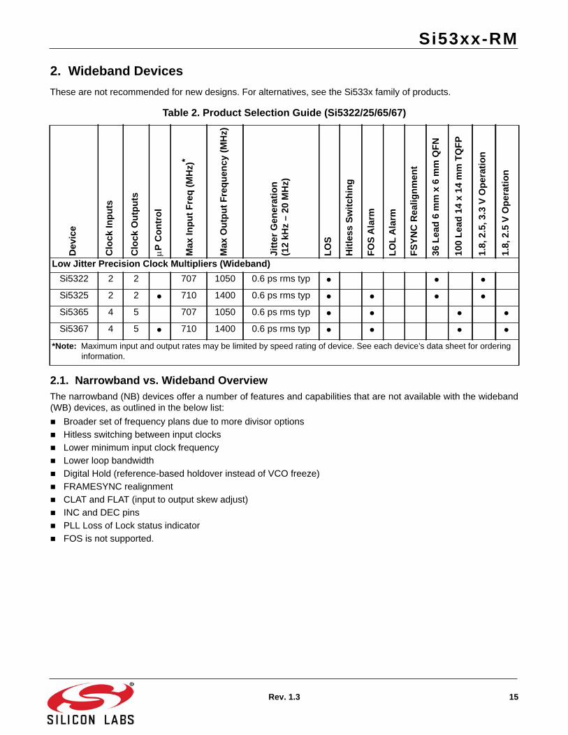
2. Wideband DevicesThese are not recommended for new designs. For alternatives, see the Si533x family of products.
2.1. Narrowband vs. Wideband OverviewThe narrowband (NB) devices offer a number of features and capabilities that are not available with the wideband(WB) devices, as outlined in the below list:
Broader set of frequency plans due to more divisor options
Hitless switching between input clocks
Lower minimum input clock frequency
Lower loop bandwidth
Digital Hold (reference-based holdover instead of VCO freeze)
FRAMESYNC realignment
CLAT and FLAT (input to output skew adjust)
INC and DEC pins
PLL Loss of Lock status indicator
FOS is not supported.
Table 2. Product Selection Guide (Si5322/25/65/67)
Dev
ice
Clo
ck In
puts
Clo
ck O
utpu
ts
P C
ontr
ol
Max
Inpu
t Fre
q (M
Hz)
*
Max
Out
put F
requ
ency
(MH
z)
Jitte
r Gen
erat
ion
(12
kHz
– 20
MH
z)
LOS
Hitl
ess
Switc
hing
FOS
Ala
rm
LOL
Ala
rm
FSYN
C R
ealig
nmen
t
36 L
ead
6 m
m x
6 m
m Q
FN
100
Lead
14
x 14
mm
TQ
FP
1.8,
2.5
, 3.3
V O
pera
tion
1.8,
2.5
V O
pera
tion
Low Jitter Precision Clock Multipliers (Wideband)Si5322 2 2 707 1050 0.6 ps rms typ Si5325 2 2 710 1400 0.6 ps rms typ Si5365 4 5 707 1050 0.6 ps rms typ Si5367 4 5 710 1400 0.6 ps rms typ
*Note: Maximum input and output rates may be limited by speed rating of device. See each device’s data sheet for ordering information.

Si53xx-RM
16 Rev. 1.3
3. Any-Frequency Clock Family Members3.1. Si5316The Si5316 is a low jitter, precision jitter attenuator for high-speed communication systems, including OC-48, OC-192, 10G Ethernet, and 10G Fibre Channel. The Si5316 accepts dual clock inputs in the 19, 38, 77, 155, 311, or622 MHz frequency range and generates a jitter-attenuated clock output at the same frequency. Within each ofthese clock ranges, the device can be tuned approximately 14% higher than nominal SONET/SDH frequencies, upto a maximum of 710 MHz in the 622 MHz range. The DSPLL loop bandwidth is digitally selectable, providing jitterperformance optimization at the application level. Operating from a single 1.8, 2.5, or 3.3 V supply, the Si5316 isideal for providing jitter attenuation in high performance timing applications. See "5. Pin Control Parts (Si5316,Si5322, Si5323, Si5365, Si5366)" on page 37 for a complete description.
Figure 1. Si5316 Any-Frequency Jitter Attenuator Block Diagram

Si53xx-RM
Rev. 1.3 17
3.2. Si5319The Si5319 is a jitter-attenuating precision M/N clock multiplier for applications requiring sub 1 ps jitterperformance. The Si5319 accepts one clock input ranging from 2 kHz to 710 MHz and generates one clock outputranging from 2 kHz to 945 MHz and select frequencies to 1.4 GHz. The Si5319 can also use its crystal oscillator asa clock source for frequency synthesis. The device provides virtually any frequency translation combination acrossthis operating range. The Si5319 input clock frequency and clock multiplication ratio are programmable through anI2C or SPI interface. The Si5319 is based on Silicon Laboratories' 3rd-generation DSPLL® technology, whichprovides any-frequency synthesis and jitter attenuation in a highly integrated PLL solution that eliminates the needfor external VCXO and loop filter components. The DSPLL loop bandwidth is digitally programmable, providingjitter performance optimization at the application level. Operating from a single 1.8, 2.5, or 3.3 V supply, the Si5319is ideal for providing clock multiplication and jitter attenuation in high performance timing applications. See "6.Microprocessor Controlled Parts (Si5319, Si5324, Si5325, Si5326, Si5327, Si5328, Si5367, Si5368, Si5369,Si5374, Si5375, and Si5376)" on page 63 for a complete description.
Figure 2. Si5319 Any-Frequency Jitter Attenuating Clock Multiplier Block Diagram

Si53xx-RM
18 Rev. 1.3
3.3. Si5322The Si5322 is a low jitter, precision clock multiplier for applications requiring clock multiplication without jitterattenuation. The Si5322 accepts dual clock inputs ranging from 19.44 to 707 MHz and generates two frequency-multiplied clock outputs ranging from 19.44 to 1050 MHz. The input clock frequency and clock multiplication ratioare selectable from a table of popular SONET, Ethernet, Fibre Channel, and broadcast video (HD SDI, 3G SDI)rates. The DSPLL loop bandwidth is digitally selectable from 150 kHz to 1.3 MHz. Operating from a single 1.8, 2.5,or 3.3 V supply, the Si5322 is ideal for providing low jitter clock multiplication in high performance timingapplications. See "5. Pin Control Parts (Si5316, Si5322, Si5323, Si5365, Si5366)" on page 37 for a completedescription.
Figure 3. Si5322 Low Jitter Clock Multiplier Block DiagramNote: Not recommended for new designs. For alternatives, see the Si533x family of products.

Si53xx-RM
Rev. 1.3 19
3.4. Si5323The Si5323 is a jitter-attenuating precision clock multiplier for high-speed communication systems, includingSONET OC-48/OC-192, Ethernet, Fibre Channel, and broadcast video (HD SDI, 3G SDI). The Si5323 acceptsdual clock inputs ranging from 8 kHz to 707 MHz and generates two frequency-multiplied clock outputs rangingfrom 8 kHz to 1050 MHz. The input clock frequency and clock multiplication ratio are selectable from a table ofpopular SONET, Ethernet, Fibre Channel, and broadcast video rates. The DSPLL loop bandwidth is digitallyselectable, providing jitter performance optimization at the application level. Operating from a single 1.8, 2.5, or3.3 V supply, the Si5323 is ideal for providing clock multiplication and jitter attenuation in high-performance timingapplications. See "5. Pin Control Parts (Si5316, Si5322, Si5323, Si5365, Si5366)" on page 37 for a completedescription.
Figure 4. Si5323 Jitter Attenuating Clock Multiplier Block Diagram

Si53xx-RM
20 Rev. 1.3
3.5. Si5324The Si5324 is a jitter-attenuating precision clock multiplier for applications requiring sub 1 ps jitter performance.The Si5324 accepts dual clock inputs ranging from 2 kHz to 710 MHz and generates two independent,synchronous clock outputs ranging from 2 kHz to 945 MHz and select frequencies to 1.4 GHz. The device providesvirtually any frequency translation combination across this operating range. The Si5324 input clock frequency andclock multiplication ratios are programmable through an I2C or SPI interface. The DSPLL loop bandwidth is digitallyprogrammable, providing jitter performance optimization at the application level. The Si5324 features loopbandwidth values as low as 4 Hz. Operating from a single 1.8, 2.5, or 3.3 V supply, the Si5324 is ideal for providingclock multiplication and jitter attenuation in high-performance timing applications. See "6. MicroprocessorControlled Parts (Si5319, Si5324, Si5325, Si5326, Si5327, Si5328, Si5367, Si5368, Si5369, Si5374, Si5375, andSi5376)" on page 63 for a complete description.
Figure 5. Si5324 Clock Multiplier and Jitter Attenuator Block Diagram

Si53xx-RM
Rev. 1.3 21
3.6. Si5325The Si5325 is a low jitter, precision clock multiplier for applications requiring clock multiplication without jitterattenuation. The Si5325 accepts dual clock inputs ranging from 10 to 710 MHz and generates two independent,synchronous clock outputs ranging from 2 kHz to 945 MHz and select frequencies to 1.4 GHz. The Si5325 inputclock frequency and clock multiplication ratios are programmable through an I2C or SPI interface. The DSPLL loopbandwidth is digitally programmable from 150 kHz to 1.3 MHz. Operating from a single 1.8, 2.5, or 3.3 V supply, theSi5325 is ideal for providing clock multiplication in high performance timing applications. See "6. MicroprocessorControlled Parts (Si5319, Si5324, Si5325, Si5326, Si5327, Si5328, Si5367, Si5368, Si5369, Si5374, Si5375, andSi5376)" on page 63 for a complete description.
Figure 6. Si5325 Low Jitter Clock Multiplier Block DiagramNote: Not recommended for new designs. For alternatives, see the Si533x family of products.

Si53xx-RM
22 Rev. 1.3
3.7. Si5326The Si5326 is a jitter-attenuating precision clock multiplier for applications requiring sub 1 ps jitter performance.The Si5326 accepts dual clock inputs ranging from 2 kHz to 710 MHz and generates two independent,synchronous clock outputs ranging from 2 kHz to 945 MHz and select frequencies to 1.4 GHz. The device providesvirtually any frequency translation combination across this operating range. The Si5326 input clock frequency andclock multiplication ratios are programmable through an I2C or SPI interface. The DSPLL loop bandwidth is digitallyprogrammable from 60 Hz to 8 kHz, providing jitter performance optimization at the application level. Operatingfrom a single 1.8, 2.5, or 3.3 V supply, the Si5326 is ideal for providing clock multiplication and jitter attenuation inhigh-performance timing applications. See "6. Microprocessor Controlled Parts (Si5319, Si5324, Si5325, Si5326,Si5327, Si5328, Si5367, Si5368, Si5369, Si5374, Si5375, and Si5376)" on page 63 for a complete description.
Figure 7. Si5326 Clock Multiplier and Jitter Attenuator Block Diagram

Si53xx-RM
Rev. 1.3 23
3.8. Si5327The Si5327 is a jitter-attenuating precision clock multiplier for applications requiring sub 1 ps jitter performance.The Si5327 accepts dual clock inputs ranging from 2 kHz to 710 MHz and generates two independent,synchronous clock outputs ranging from 2 kHz to 808 MHz. The device provides virtually any frequency translationcombination across this operating range. The Si5327 input clock frequency and clock multiplication ratios areprogrammable through an I2C or SPI interface. The DSPLL loop bandwidth is digitally programmable, providingjitter performance optimization at the application level. The Si5327 features loop bandwidth values as low as 4 Hz.Operating from a single 1.8, 2.5, or 3.3 V supply, the Si5327 is ideal for providing clock multiplication and jitterattenuation in high-performance timing applications. See "6. Microprocessor Controlled Parts (Si5319, Si5324,Si5325, Si5326, Si5327, Si5328, Si5367, Si5368, Si5369, Si5374, Si5375, and Si5376)" on page 63 for a completedescription.
Figure 8. Si5327 Clock Multiplier and Jitter Attenuator Block Diagram

Si53xx-RM
24 Rev. 1.3
3.9. Si5328The Si5328 is a jitter-attenuating precision clock multiplier for applications requiring sub-1 ps jitter performance anddigitally-programmable ultra-low-loop BW ranging from 0.05 to 6 Hz. When combined with a low-wander, low-jitterreference oscillator, the Si5328 meets all of the wander, MTIE, TDEV, and other requirements that are listed in ITU-T G.8262. The Si5328 accepts two input clocks ranging from 8 kHz to 346 MHz and generates two output clocksranging from 2 kHz to 346 MHz. The device provides virtually any frequency translation combination across theoperating range. The Si5328 input clock frequency and clock multiplication ratio are programmable through andI2C or SPI interface. Operating from a single 1.8, 2.5, or 3.3 V supply, the Si5328 is ideal for providing multiplicationand jitter/wander attenuation in high-performance timing applications like SyncE timing cards. See "6.Microprocessor Controlled Parts (Si5319, Si5324, Si5325, Si5326, Si5327, Si5328, Si5367, Si5368, Si5369,Si5374, Si5375, and Si5376)" on page 63 for a complete description. Also see “AN775: Si5328 ITU-T G.8261SyncE Compliance Test Report" and “AN776: Using the Si5328 in a G.8262 Compliant SyncE Application".
Figure 9. Si5328 Clock Multiplier and Jitter Attenuator Block Diagram
Si53xx-RM
Rev. 1.3 25
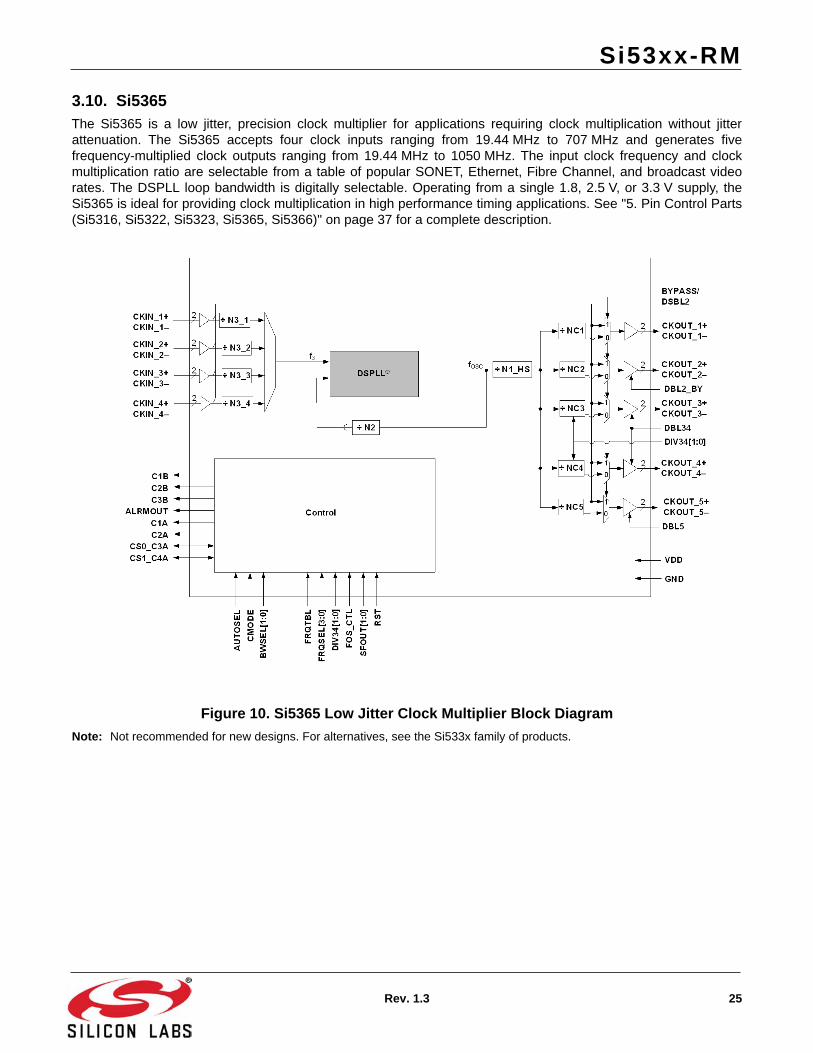
3.10. Si5365The Si5365 is a low jitter, precision clock multiplier for applications requiring clock multiplication without jitterattenuation. The Si5365 accepts four clock inputs ranging from 19.44 MHz to 707 MHz and generates fivefrequency-multiplied clock outputs ranging from 19.44 MHz to 1050 MHz. The input clock frequency and clockmultiplication ratio are selectable from a table of popular SONET, Ethernet, Fibre Channel, and broadcast videorates. The DSPLL loop bandwidth is digitally selectable. Operating from a single 1.8, 2.5 V, or 3.3 V supply, theSi5365 is ideal for providing clock multiplication in high performance timing applications. See "5. Pin Control Parts(Si5316, Si5322, Si5323, Si5365, Si5366)" on page 37 for a complete description.
Figure 10. Si5365 Low Jitter Clock Multiplier Block DiagramNote: Not recommended for new designs. For alternatives, see the Si533x family of products.

Si53xx-RM
26 Rev. 1.3
3.11. Si5366The Si5366 is a jitter-attenuating precision clock multiplier for high-speed communication systems, includingSONET OC-48/OC-192, Ethernet, and Fibre Channel. The Si5366 accepts four clock inputs ranging from 8 kHz to707 MHz and generates five frequency-multiplied clock outputs ranging from 8 kHz to 1050 MHz. The input clockfrequency and clock multiplication ratio are selectable from a table of popular SONET, Ethernet, Fibre Channel,and broadcast video (HD SDI, 3G SDI) rates. The DSPLL loop bandwidth is digitally selectable from 60 Hz to8 kHz, providing jitter performance optimization at the application level. Operating from a single 1.8, 2.5, or 3.3 Vsupply, the Si5366 is ideal for providing clock multiplication and jitter attenuation in high performance timingapplications. See "5. Pin Control Parts (Si5316, Si5322, Si5323, Si5365, Si5366)" on page 37 for a completedescription.
Figure 11. Si5366 Jitter Attenuating Clock Multiplier Block Diagram
Si53xx-RM
Rev. 1.3 27
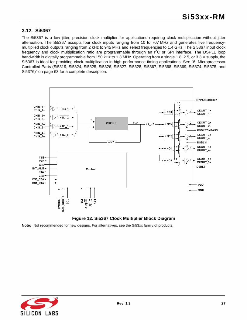
3.12. Si5367The Si5367 is a low jitter, precision clock multiplier for applications requiring clock multiplication without jitterattenuation. The Si5367 accepts four clock inputs ranging from 10 to 707 MHz and generates five frequency-multiplied clock outputs ranging from 2 kHz to 945 MHz and select frequencies to 1.4 GHz. The Si5367 input clockfrequency and clock multiplication ratio are programmable through an I2C or SPI interface. The DSPLL loopbandwidth is digitally programmable from 150 kHz to 1.3 MHz. Operating from a single 1.8, 2.5, or 3.3 V supply, theSi5367 is ideal for providing clock multiplication in high performance timing applications. See "6. MicroprocessorControlled Parts (Si5319, Si5324, Si5325, Si5326, Si5327, Si5328, Si5367, Si5368, Si5369, Si5374, Si5375, andSi5376)" on page 63 for a complete description.
Figure 12. Si5367 Clock Multiplier Block DiagramNote: Not recommended for new designs. For alternatives, see the Si53xx family of products.

Si53xx-RM
28 Rev. 1.3
3.13. Si5368The Si5368 is a jitter-attenuating precision clock multiplier for applications requiring sub 1 ps rms jitterperformance. The Si5368 accepts four clock inputs ranging from 2 kHz to 710 MHz and generates fiveindependent, synchronous clock outputs ranging from 2 kHz to 945 MHz and select frequencies to 1.4 GHz. Thedevice provides virtually any frequency translation combination across this operating range. The Si5368 input clockfrequency and clock multiplication ratio are programmable through an I2C or SPI interface. The DSPLL loopbandwidth is digitally programmable from 60 Hz to 8 kHz, providing jitter performance optimization at theapplication level. Operating from a single 1.8, 2.5, or 3.3 V supply, the Si5368 is ideal for providing clockmultiplication and jitter attenuation in high performance timing applications. See "6. Microprocessor ControlledParts (Si5319, Si5324, Si5325, Si5326, Si5327, Si5328, Si5367, Si5368, Si5369, Si5374, Si5375, and Si5376)" onpage 63 for a complete description.
Figure 13. Si5368 Clock Multiplier and Jitter Attenuator Block Diagram

Si53xx-RM
Rev. 1.3 29
3.14. Si5369The Si5369 is a jitter-attenuating precision clock multiplier for applications requiring sub 1 ps rms jitterperformance. The Si5369 accepts four clock inputs ranging from 2 kHz to 710 MHz and generates fiveindependent, synchronous clock outputs ranging from 2 kHz to 945 MHz and select frequencies to 1.4 GHz. Thedevice provides virtually any frequency translation combination across this operating range. The Si5369 input clockfrequency and clock multiplication ratio are programmable through an I2C or SPI interface. The DSPLL loopbandwidth is digitally programmable, providing loop bandwidth values as low as 4 Hz. Operating from a single 1.8,2.5, or 3.3 V supply, the Si5369 is ideal for providing clock multiplication and jitter attenuation in high performancetiming applications. See "6. Microprocessor Controlled Parts (Si5319, Si5324, Si5325, Si5326, Si5327, Si5328,Si5367, Si5368, Si5369, Si5374, Si5375, and Si5376)" on page 63 for a complete description.
Figure 14. Si5369 Clock Multiplier and Jitter Attenuator Block Diagram
3.15. Si5374/75/76 Compared to Si5324/19/26In general, the Si5374 can be viewed as a quad version of the Si5324, and the Si5375 can be viewed as a quadversion of the Si5319, and the Si5376 can be viewed as a quad version of the Si5326. However, they are notexactly the same. This is an overview of the differences:
1. The Si5374/75/76 cannot use a crystal as its OSC reference. It requires the use of a single external single-ended or differential crystal oscillator.
2. The Si5374/75/76 only supports I2C as its serial port protocol and does not have SPI. No I2C address pins are available on the Si5374/75/76.
3. The Si5374/75/76 does not provide separate INT_CK1B and CK2B pins to indicate when CKIN1 and CKIN2 do not have valid clock inputs. Instead, the IRQ pin can be programmed to function as one pin, the other pin or both.
4. Selection of the OSC frequency is done by a register (RATE_REG), not by using the RATE pins.
5. The Si5374/75/76 uses a different version of DSPLLsim: Si537xDSPLLsim.
6. The Si5374/75/76 does not support 3.3 V operation.

Si53xx-RM
30 Rev. 1.3
3.16. Si5374The Si5374 is a highly integrated, 4-PLL jitter-attenuating precision clock multiplier for applications requiring sub 1ps jitter performance. Each of the DSPLL® clock multiplier engines accepts two input clocks ranging from 2 kHz to710 MHz and generates two independent, synchronous output clocks ranging from 2 kHz to 808 MHz. EachDSPLL provides virtually any frequency translation across this operating range. For asynchronous, free-runningclock generation applications, the Si5374’s reference oscillator can be used as a clock source for the four DSPLLs.The Si5374 input clock frequency and clock multiplication ratio are programmable through an I2C interface. TheSi5374 is based on Silicon Laboratories' 3rd-generation DSPLL® technology, which provides any-frequencysynthesis and jitter attenuation in a highly integrated PLL solution that eliminates the need for external VCXO andloop filter components. Each DSPLL loop bandwidth is digitally programmable from 4 to 525 Hz, providing jitterperformance optimization at the application level. The device operates from a single 1.8 or 2.5 V supply with on-chip voltage regulators with excellent PSRR. The Si5374 is ideal for providing clock multiplication and jitterattenuation in high port count optical line cards requiring independent timing domains.
Figure 15. Si5374 Functional Block Diagram

Si53xx-RM
Rev. 1.3 31
3.17. Si5375The Si5375 is a highly integrated, 4-PLL jitter-attenuating precision clock multiplier for applications requiring sub 1ps jitter performance. Each of the DSPLL® clock multiplier engines accepts an input clock ranging from 2 kHz to710 MHz and generates an output clock ranging from 2 kHz to 808 MHz. Each DSPLL provides virtually anyfrequency translation combination across this operating range. For asynchronous, free-running clock generationapplications, the Si5375’s reference oscillator can be used as a clock source for any of the four DSPLLs. TheSi5375 input clock frequency and clock multiplication ratio are programmable through an I2C interface. The Si5375is based on Silicon Laboratories' third-generation DSPLL® technology, which provides any-frequency synthesisand jitter attenuation in a highly integrated PLL solution that eliminates the need for external VCXO and loop filtercomponents. Each DSPLL loop bandwidth is digitally programmable from 60 Hz to 8 kHz, providing jitterperformance optimization at the application level. The device operates from a single 1.8 or 2.5 V supply with on-chip voltage regulators with excellent PSRR. The Si5375 is ideal for providing clock multiplication and jitterattenuation in high port count optical line cards requiring independent timing domains.
Figure 16. Si5375 Functional Block Diagram

Si53xx-RM
32 Rev. 1.3
3.18. Si5376The Si5376 is a highly integrated, 4-PLL jitter-attenuating precision clock multiplier for applications requiring sub 1ps jitter performance. Each of the DSPLL® clock multiplier engines accepts two input clocks ranging from 2 kHz to710 MHz and generates two independent, synchronous output clocks ranging from 2 kHz to 808 MHz. EachDSPLL provides virtually any frequency translation across this operating range. For asynchronous, free-runningclock generation applications, the Si5376’s reference oscillator can be used as a clock source for the four DSPLLs.The Si5376 input clock frequency and clock multiplication ratio are programmable through an I2C interface. TheSi5376 is based on Silicon Laboratories' 3rd-generation DSPLL® technology, which provides any-frequencysynthesis and jitter attenuation in a highly integrated PLL solution that eliminates the need for external VCXO andloop filter components. Each DSPLL loop bandwidth is digitally programmable from 60 Hz to 8 kHz, providing jitterperformance optimization at the application level. The device operates from a single 1.8 or 2.5 V supply with on-chip voltage regulators with excellent PSRR. The Si5376 is ideal for providing clock multiplication and jitterattenuation in high port count optical line cards requiring independent timing domains.
Figure 17. Si5376 Functional Block Diagram

Si53xx-RM
Rev. 1.3 33
4. DSPLL (All Devices)All members of the Any-Frequency Precision Clocks family incorporate a phase-locked loop (PLL) that utilizesSilicon Laboratories' third generation DSPLL technology to eliminate jitter, noise, and the need for external VCXOand loop filter components found in discrete PLL implementations. This is achieved by using a digital signalprocessing (DSP) algorithm to replace the loop filter commonly found in discrete PLL designs. Because externalPLL components are not required, sensitivity to board-level noise sources is minimized. This digital technologyprovides highly stable and consistent operation over process, temperature, and voltage variations.
A simplified block diagram of the DSPLL is shown in Figure 18. This algorithm processes the phase detector errorterm and generates a digital frequency control word M to adjust the frequency of the digitally-controlled oscillator(DCO). The narrowband configuration devices (Si5316, Si5319, Si5323, Si5324, Si5326, Si5327, Si5366, Si5368,and Si5369) provide ultra-low jitter generation by using an external jitter reference clock and jitter attenuation. Forapplications where basic frequency multiplication of low jitter clocks is all that is required, the wideband parts(Si5322, Si5325, Si5365, and Si5367) are available.
Figure 18. Any-Frequency Precision Clock DSPLL Block Diagram

Si53xx-RM
34 Rev. 1.3
4.1. Clock MultiplicationFundamental to these parts is a clock multiplication circuit that is simplified in Figure 19. By having a large range ofdividers and multipliers, nearly any output frequency can be created from a fixed input frequency. For typicaltelecommunications and data communications applications, the hardware control parts (Si5316, Si5322, Si5323,Si5365, and Si5366) provide simple pin control.
The microprocessor controlled parts (Si5319, Si5324, Si5325, Si5326, Si5327, Si5367, Si5368, and Si5369)provide a programmable range of clock multiplications. To assist users in finding valid divider settings for aparticular input frequency and clock multiplication ratio, Silicon Laboratories offers PC-based software (DSPLLsim)that calculates these settings automatically. When multiple divider combinations produce the same outputfrequency, the software recommends the divider settings yielding the recommended settings for phase noiseperformance and power consumption.
Figure 19. Clock Multiplication Circuit

Si53xx-RM
Rev. 1.3 35
4.2. PLL PerformanceAll members of the Any-Frequency Precision Clock family of devices provide extremely low jitter generation, a well-controlled jitter transfer function, and high jitter tolerance. For more information the loop bandwidth and its effect onjitter attenuation, see "Appendix H—Jitter Attenuation and Loop BW" on page 160.
4.2.1. Jitter GenerationJitter generation is defined as the amount of jitter produced at the output of the device with a jitter free input clock.Generated jitter arises from sources within the VCO and other PLL components. Jitter generation is a function ofthe PLL bandwidth setting. Higher loop bandwidth settings may result in lower jitter generation, but may result inless attenuation of jitter that might be present on the input clock signal.
4.2.2. Jitter TransferJitter transfer is defined as the ratio of output signal jitter to input signal jitter for a specified jitter frequency. Thejitter transfer characteristic determines the amount of input clock jitter that passes to the outputs. The DSPLLtechnology used in the Any-Frequency Precision Clock devices provides tightly controlled jitter transfer curvesbecause the PLL gain parameters are determined largely by digital circuits which do not vary over supply voltage,process, and temperature. In a system application, a well-controlled transfer curve minimizes the output clock jittervariation from board to board and provides more consistent system level jitter performance.
The jitter transfer characteristic is a function of the loop bandwidth setting. Lower bandwidth settings result in morejitter attenuation of the incoming clock, but may result in higher jitter generation. Section 1 Any-FrequencyPrecision Clock Product Family Overview also includes specifications related to jitter bandwidth and peaking.Figure 20 shows the jitter transfer curve mask.
Figure 20. PLL Jitter Transfer Mask/Template

Si53xx-RM
36 Rev. 1.3
4.2.3. Jitter ToleranceJitter tolerance is defined as the maximum peak-to-peak sinusoidal jitter that can be present on the incoming clockbefore the DSPLL loses lock. The tolerance is a function of the jitter frequency, because tolerance improves forlower input jitter frequency.
The jitter tolerance of the DSPLL is a function of the loop bandwidth setting. Figure 21 shows the general shape ofthe jitter tolerance curve versus input jitter frequency. For jitter frequencies above the loop bandwidth, the toleranceis a constant value Aj0. Beginning at the PLL bandwidth, the tolerance increases at a rate of 20 dB/decade forlower input jitter frequencies.
Figure 21. Jitter Tolerance Mask/TemplateThe equation for the high frequency jitter tolerance can be expressed as a function of the PLL loop bandwidth (i.e.,bandwidth):
For example, the jitter tolerance when fin = 155.52 MHz, fout = 622.08 MHz and the loop bandwidth (BW) is 100 Hz:
Aj05000BW------------- ns pk-pk=
Aj05000100
------------- 50 ns pk-pk= =

Si53xx-RM
Rev. 1.3 37
5. Pin Control Parts (Si5316, Si5322, Si5323, Si5365, Si5366)These parts provide high-performance clock multiplication with simple pin control. Many of the control inputs arethree levels: High, Low, and Medium. High and Low are standard voltage levels determined by the supply voltage:VDD and Ground. If the input pin is left floating, it is driven to nominally half of VDD. Effectively, this creates threelogic levels for these controls.
These parts span a range of applications and I/O capacity as shown in Table 3.
5.1. Clock Multiplication (Si5316, Si5322, Si5323, Si5365, Si5366)By setting the tri-level FRQSEL[3:0] pins these devices provide a wide range of standard SONET and datacommunications frequency scaling, including simple integer frequency multiplication to fractional settings requiredfor coding and decoding.
5.1.1. Clock Multiplication (Si5316)The device accepts dual input clocks in the 19, 39, 78, 155, 311, or 622 MHz frequency range and generates a de-jittered output clock at the same frequency. The frequency range is set by the FRQSEL [1:0] pins, as shown inTable 4.
Table 3. Si5316, Si5322, Si5323, Si5365 and Si5366 Key Features
Si5316 Si5322 Si5323 Si5365 Si5366
SONET Frequencies
DATACOM Frequencies
DATACOM/SONET internetworking
Fixed Ratio between input clocks
Flexible Frequency Plan
Number of Inputs 2 2 2 4 4
Number of Outputs 1 2 2 5 5
Jitter Attenuation
Table 4. Frequency Settings
FRQSEL[1:0] Output Frequency (MHz)
LL 19.38–22.28
LM 38.75–44.56
LH 77.50–89.13
ML 155.00–178.25
MM 310.00–356.50
MH 620.00–710.00

Si53xx-RM
38 Rev. 1.3
The Si5316 can accept a CKIN1 input at a different frequency than the CKIN2 input. The frequency of one inputclock can be 1x, 4x, or 32x the frequency of the other input clock. The output frequency is always equal to the lowerof the two clock inputs and is set via the FRQSEL [1:0] pins. The frequency applied at each clock input is divideddown by a pre-divider as shown in the Figure 1 on page 16. These pre-dividers must be set such that the tworesulting clock frequencies, f3_1 and f3_2 must be equal and are set by the FRQSEL [1:0] pins. Input dividersettings are controlled by the CK1DIV and CK2DIV pins, as shown in Table 5.
Figure 22. Si5316 Divisor Ratios
Table 5. Input Divider Settings
CKnDIV N3n Input Divider
L 1
M 4
H 32
Table 6. Si5316 Bandwidth Values
FRQSEL[1:0] Nominal Frequency Values (MHz)
LL LM LH ML MM MH
BW[1:0] 19.44 MHz 38.88 MHz 77.76 MHz 155.52 MHz 311.04 MHz 622.08 MHz
HM 100 Hz 100 Hz 100 Hz 100 Hz 100 Hz 100 Hz
HL 210 Hz 210 Hz 200 Hz 200 Hz 200 Hz 200 Hz
MH 410 Hz 410 Hz 400 Hz 400 Hz 400 Hz 400 Hz
MM 1.7 kHz 1.7 kHz 1.6 kHz 1.6 kHz 1.6 kHz 1.6 kHz
ML 7.0 kHz 7.0 kHz 6.8 kHz 6.7 kHz 6.7 kHz 6.7 kHz

Si53xx-RM
Rev. 1.3 39
5.1.2. Clock Multiplication (Si5322, Si5323, Si5365, Si5366)These parts provide flexible frequency plans for SONET, DATACOM, and interworking between the two (Table 7, Table 8, and Table 9 respectively). The CKINn inputs must be the same frequency as specified in the tables. Theoutputs are the same frequency; however, in the Si5365 and Si5366, CKOUT3 and CKOUT4 can be further divideddown by using the DIV34 [1:0] pins.
The following notes apply to Tables 7, 8, and 9:
1. All entries are available for the Si5323 and Si5366. Only those marked entries under the WB column are available for the Si5322 and Si5365.
2. The listed output frequencies appear on CKOUTn. For the Si5365 and Si5366, sub-multiples are available on CKOUT3 and CKOUT4 using the DIV34[1:0] control pins.
3. All ratios are exact, but the frequency values are rounded.
4. For bandwidth settings, f3 values, and frequency operating ranges, consult DSPLLsim.
5. For the Si5366 with CK_CONF = 1, CKIN3 and CKIN4 are the same frequency as FS_OUT.
Table 7. SONET Clock Multiplication Settings (FRQTBL=L)
No FRQSEL[3:0]
WB
fIN MHz Mult Factor Nominal fOUT MHz
All Devices Si5366 Only
fCKOUT5 (MHz)(CK_CONF = 0)
FS_OUT (MHz)(CK_CONF = 1)
0 LLLL 0.008 1 0.008 0.008 0.008
1 LLLM 2430 19.44 19.44 0.008
2 LLLH 4860 38.88 38.88 0.008
3 LLML 9720 77.76 77.76 0.008
4 LLMM 19440 155.52 155.52 0.008
5 LLMH 38880 311.04 311.04 0.008
6 LLHL 77760 622.08 622.08 0.008

Si53xx-RM
40 Rev. 1.3
7 LLHM 19.44 1 19.44 19.44 0.008
8 LLHH 2 38.88 38.88 0.008
9 LMLL 4 77.76 77.76 0.008
10 LMLM 8 155.52 155.52 0.008
11 LMLH 8 x (255/238) 166.63 166.63 NA
12 LMML 8 x (255/237) 167.33 167.33 NA
13 LMMM 8 x (255/236) 168.04 168.04 NA
14 LMMH 16 311.04 311.04 0.008
15 LMHL 32 622.08 622.08 0.008
16 LMHM 32 x (255/238) 666.51 666.51 NA
17 LMHH 32 x (255/237) 669.33 669.33 NA
18 LHLL 32 x (255/236) 672.16 672.16 NA
19 LHLM 48 933.12 933.12 0.008
20 LHLH 54 1049.76 1049.76 0.008
21 LHML 38.88 1 38.88 38.88 0.008
22 LHMM 2 77.76 77.76 0.008
23 LHMH 4 155.52 155.52 0.008
24 LHHL 16 622.08 622.08 0.008
25 LHHM 16 x (255/238) 666.51 666.51 NA
26 LHHH 16 x (255/237) 669.33 669.33 NA
27 MLLL 16 x (255/236) 672.16 672.16 NA
Table 7. SONET Clock Multiplication Settings (FRQTBL=L) (Continued)
No FRQSEL[3:0]
WB
fIN MHz Mult Factor Nominal fOUT MHz
All Devices Si5366 Only
fCKOUT5 (MHz)(CK_CONF = 0)
FS_OUT (MHz)(CK_CONF = 1)

Si53xx-RM
Rev. 1.3 41
28 MLLM 77.76 1/4 19.44 19.44 0.008
29 MLLH 1/2 38.88 38.88 0.008
30 MLML 1 77.76 77.76 0.008
31 MLMM 2 155.52 155.52 0.008
32 MLMH 2 x (255/238) 166.63 166.63 NA
33 MLHL 2 x (255/237) 167.33 167.33 NA
34 MLHM 2 x (255/236) 168.04 168.04 NA
35 MLHH 4 311.04 311.04 0.008
36 MMLL 8 622.08 622.08 0.008
37 MMLM 8 x (255/238) 666.51 666.51 NA
38 MMLH 8 x (255/237) 669.33 669.33 NA
39 MMML 8 x (255/236) 672.16 672.16 NA
40 MMMM 155.52 1/8 19.44 19.44 0.008
41 MMMH 1/4 38.88 38.88 0.008
42 MMHL 1/2 77.76 77.76 0.008
43 MMHM 1 155.52 155.52 0.008
44 MMHH 255/238 166.63 166.63 NA
45 MHLL 255/237 167.33 167.33 NA
46 MHLM 255/236 168.04 168.04 NA
47 MHLH 2 311.04 311.04 0.008
48 MHML 4 622.08 622.08 0.008
49 MHMM 4 x (255/238) 666.51 666.51 NA
50 MHMH 4 x (255/237) 669.33 669.33 NA
51 MHHL 4 x (255/236) 672.16 672.16 NA
52 MHHM 166.63 238/255 155.52 155.52 NA
53 MMHM 1 166.63 166.63 NA
54 MHHH 4 x (238/255) 622.08 622.08 NA
55 MHML 4 666.51 666.51 NA
Table 7. SONET Clock Multiplication Settings (FRQTBL=L) (Continued)
No FRQSEL[3:0]
WB
fIN MHz Mult Factor Nominal fOUT MHz
All Devices Si5366 Only
fCKOUT5 (MHz)(CK_CONF = 0)
FS_OUT (MHz)(CK_CONF = 1)

Si53xx-RM
42 Rev. 1.3
56 HLLL 167.33 237/255 155.52 155.52 NA
57 MMHM 1 167.33 167.33 NA
58 HLLM 4 x (237/255) 622.08 622.08 NA
59 MHML 4 669.33 669.33 NA
60 HLLH 168.04 236/255 155.52 155.52 NA
61 MMHM 1 168.04 168.04 NA
62 HLML 4 x (236/255) 622.08 622.08 NA
63 MHML 4 672.16 672.16 NA
64 HLMM 311.04 1 311.04 311.04 0.008
65 HLMH 2 622.08 622.08 0.008
66 HLHL 2 x (255/238) 666.51 666.51 NA
67 HLHM 2 x (255/237) 669.33 669.33 NA
68 HLHH 2 x (255/236) 672.16 672.16 NA
69 HMLL 622.08 1/32 19.44 19.44 0.008
70 HMLM 1/16 38.88 38.88 0.008
71 HMLH 1/8 77.76 77.76 0.008
72 HMML 1/4 155.52 155.52 0.008
73 HMMM 1/2 311.04 311.04 0.008
74 HMMH 1 622.08 622.08 0.008
75 HMHL 255/238 666.51 666.51 NA
76 HMHM 255/237 669.33 669.33 NA
77 HMHH 255/236 672.16 672.16 NA
78 HHLL 666.51 1/4 x 238/255 155.52 155.52 NA
79 HMML 1/4 166.63 166.63 NA
80 HHLM 238/255 622.08 622.08 NA
81 HMMH 1 666.51 666.51 NA
Table 7. SONET Clock Multiplication Settings (FRQTBL=L) (Continued)
No FRQSEL[3:0]
WB
fIN MHz Mult Factor Nominal fOUT MHz
All Devices Si5366 Only
fCKOUT5 (MHz)(CK_CONF = 0)
FS_OUT (MHz)(CK_CONF = 1)

Si53xx-RM
Rev. 1.3 43
82 HHLH 669.33 1/4 x 237/255 155.52 155.52 NA
83 HMML 1/4 167.33 167.33 NA
84 HHML 237/255 622.08 622.08 NA
85 HMMH 1 669.33 669.33 NA
86 HHMM 672.16 1/4 x 236/255 155.52 155.52 NA
87 HMML 1/4 168.04 168.04 NA
88 HHMH 236/255 622.08 622.08 NA
89 HMMH 1 672.16 672.16 NA
Table 7. SONET Clock Multiplication Settings (FRQTBL=L) (Continued)
No FRQSEL[3:0]
WB
fIN MHz Mult Factor Nominal fOUT MHz
All Devices Si5366 Only
fCKOUT5 (MHz)(CK_CONF = 0)
FS_OUT (MHz)(CK_CONF = 1)

Si53xx-RM
44 Rev. 1.3
Table 8. Datacom Clock Multiplication Settings (FRQTBL = M, CK_CONF = 0)
Setting FRQSEL[3:0]
WB fIN (MHz) Mult Factor fOUT* (MHz)
0 LLLL 15.625 2 31.25
1 LLLM 4 62.5
2 LLLH 8 125
3 LLML 16 250
4 LLMM 25 17/4 106.25
5 LLMH 5 125
6 LLHL 25/4 x 66/64 161.13
7 LLHM 51/8 x 66/64 164.36
8 LLHH 25/4 x 66/64 x 255/238 172.64
9 LMLL 25/4 x 66/64 x 255/237 173.37
10 LMLM 51/8 x 66/64 x 255/238 176.1
11 LMLH 51/8 x 66/64 x 255/237 176.84
12 LMML 17/2 212.5
13 LMMM 17 425
14 LMMH 25 x 66/64 644.53
15 LMHL 51/2 x 66/64 657.42
16 LMHM 25 x 66/64 x 255/238 690.57
17 LMHH 25 x 66/64 x 255/237 693.48
18 LHLL 51/2 x 66/64 x 255/238 704.38
19 LHLM 51/2 x 66/64 x 255/237 707.35
20 LHLH 31.25 2 62.5
21 LHML 4 125
22 LHMM 8 250
23 LHMH 53.125 2 106.25
24 LHHL 4 212.5
25 LHHM 8 425
26 LHHH 106.25 3/2 x 66/64 164.36
27 MLLL 3/2 x 66/64 x 255/238 176.1
28 MLLM 3/2 x 66/64 x 255/237 176.84
29 MLLH 2 212.5
30 MLML 4 425
31 MLMM 6 x 66/64 657.42
32 MLMH 6 x 66/64 x 255/238 704.38
33 MLHL 6 x 66/64 x 255/237 707.35

Si53xx-RM
Rev. 1.3 45
34 MLHM 125 10/8 x 66/64 161.13
35 MLHH 10/8 x 66/64 x 255/238 172.64
36 MMLL 10/8 x 66/64 x 255/237 173.37
37 MMLM 5 x 66/64 644.53
38 MMLH 5 x 66/64 x 255/238 690.57
39 MMML 5 x 66/64 x 255/237 693.48
40 MMMM 156.25 66/64 161.13
41 MMMH 66/64 x 255/238 172.64
42 MMHL 66/64 x 255/237 173.37
43 MMHM 4 x 66/64 644.53
44 MMHH 4 x 66/64 x 255/238 690.57
45 MHLL 4 x 66/64 x 255/237 693.48
46 MMMM 159.375 66/64 164.36
47 MMMH 66/64 x 255/238 176.1
48 MMHL 66/64 x 255/237 176.84
49 MMHM 4 x 66/64 657.4
50 MMHH 4 x 66/64 x 255/238 704.38
51 MHLL 4 x 66/64 x 255/237 707.35
52 MHLM 161.13 4/5 x 64/66 125
53 MHLH 255/238 172.64
54 MHML 255/237 173.37
55 MHMM 4 644.53
56 MHMH 4 x 255/238 690.57
57 MHHL 4 x 255/237 693.48
58 MHHM 164.36 2/3 x 64/66 106.25
59 MHLH 255/238 176.1
60 MHML 255/237 176.84
61 MHMM 4 657.42
62 MHMH 4 x 255/238 704.38
63 MHHL 4 x 255/237 707.35
64 MHHH 172.64 4/5 x 64/66 x 238/255 125
65 HLLL 64/66 x 238/255 156.25
66 HLLM 238/255 161.13
67 HLLH 4 x 238/255 644.53
68 MHMM 4 690.57
Table 8. Datacom Clock Multiplication Settings (FRQTBL = M, CK_CONF = 0) (Continued)
Setting FRQSEL[3:0]
WB fIN (MHz) Mult Factor fOUT* (MHz)

Si53xx-RM
46 Rev. 1.3
69 HLML 173.37 4/5 x 64/66 x 237/255 125
70 HLMM 64/66 x 237/255 156.25
71 HLMH 237/255 161.13
72 HLHL 4 x 237/255 644.53
73 MHMM 4 693.48
74 HLHM 176.1 2/3 x 64/66 x 238/255 106.25
75 HLLL 64/66 x 238/255 159.375
76 HLLM 238/255 164.36
77 HLLH 4 x 238/255 657.42
78 MHMM 4 704.38
79 HLHH 176.84 2/3 x 64/66 x 237/255 106.25
80 HLMM 64/66 x 237/255 159.375
81 HLMH 237/255 164.36
82 HLHL 4 x 237/255 657.42
83 MHMM 4 707.35
84 HMLL 212.5 2 425
85 HMLM 425 1 425
86 HMLH 644.53 1/5 x 64/66 125
87 HMML 1/4 161.13
88 HMMM 1 644.53
89 HMMH 255/238 690.57
90 HMHL 255/237 693.48
91 HMHM 657.42 1/6 x 64/66 106.25
92 HMML 1/4 164.36
93 HMMM 1 657.42
94 HMMH 255/238 704.38
95 HMHL 255/237 707.35
96 HMHH 690.57 1/5 x 64/66 x 238/255 125
97 HHLL 1/4 x 64/66 x 238/255 156.25
98 HHLM 1/4 x 238/255 161.13
99 HMML 1/4 172.64
100 HHLH 238/255 644.53
101 HMMM 1 690.57
Table 8. Datacom Clock Multiplication Settings (FRQTBL = M, CK_CONF = 0) (Continued)
Setting FRQSEL[3:0]
WB fIN (MHz) Mult Factor fOUT* (MHz)

Si53xx-RM
Rev. 1.3 47
102 HHML 693.48 1/5 x 64/66 x 237/255 125
103 HHMM 1/4 x 64/66 x 237/255 156.25
104 HHMH 1/4 x 237/255 161.13
105 HMML 1/4 173.37
106 HHHL 237/255 644.53
107 HMMM 1 693.48
108 HHHM 704.38 1/6 x 64/66 x 238/255 106.25
109 HHLL 1/4 x 64/66 x 238/255 159.375
110 HHLM 1/4 x (238/255) 164.36
111 HMML 1/4 176.1
112 HHLH 238/255 657.42
113 HMMM 1 704.38
114 HHHH 707.35 1/6 x 64/66 x 237/255 106.25
115 HHMM 1/4 x 64/66 x 237/255 159.375
116 HHMH 1/4 x (237/255) 164.36
117 HMML 1/4 176.84
118 HHHL 237/255 657.42
119 HMMM 1 707.35
Table 8. Datacom Clock Multiplication Settings (FRQTBL = M, CK_CONF = 0) (Continued)
Setting FRQSEL[3:0]
WB fIN (MHz) Mult Factor fOUT* (MHz)

Si53xx-RM
48 Rev. 1.3
Table 9. SONET to Datacom Clock Multiplication Settings
Setting FRQSEL[3:0]
WB fIN (MHz) Mult Factor fOUT* (MHz)
0 LLLL 0.008 3125 25
1 LLLM 6480 51.84
2 LLLH 53125/8 53.125
3 LLML 15625/2 62.5
4 LLMM 53125/4 106.25
5 LLMH 15625 125
6 LLHL 78125/4 156.25
7 LLHM 159375/8 159.375
8 LLHH 53125/2 212.5
9 LMLL 53125 425
10 LMLM 19.440 625/486 25
11 LMLH 10625/3888 53.125
12 LMML 3125/972 62.5
13 LMMM 10625/1944 106.25
14 LMMH 3125/486 125
15 LMHL 15625/1944 156.25
16 LMHM 31875/3888 159.375
17 LMHH 15625/1944 x 66/64 161.13
18 LHLL 31875/3888 x 66/64 164.36
19 LHLM 15625/1944 x 66/64 x 255/238
172.64
20 LHLH 31875/3888 x 66/64 x 255/238
176.1
21 LHML 10625/972 212.5
22 LHMM 10625/486 425
23 LHMH 15625/486 x 66/64 644.53
24 LHHL 31875/972 x 66/64 657.42
25 LHHM 15625/486 x 66/64 x 255/238
690.57
26 LHHH 31875/972 x 66/64 x 255/238
704.38
27 MLLL 27.000 1 27
28 MLLM 250/91 74.17582
29 MLLH 11/4 74.25

Si53xx-RM
Rev. 1.3 49
30 MLML 62.500 2 125
31 MLMM 4 250
32 MLMH 74.176 91/250 27
33 MLHL 1 74.17582
34 MLHM 91 x 11/250 x 4 74.25
35 MLHH 74.250 4/11 27
36 MMLL 4 x 250/11 x 91 74.17582
37 MMLM 1 74.25
38 MMLH 77.760 10625/7776 106.25
39 MMML 3125/1944 125
40 MMMM 15625/7776 156.25
41 MMMH 31875/15552 159.375
42 MMHL 15625/7776 x 66/64 161.13
43 MMHM 31875/15552 x 66/64 164.36
44 MMHH 15625/7776 x 66/64 x 255/238
172.64
45 MHLL 31875/15552 x 66/64 x 255/238
176.1
46 MHLM 10625/3888 212.5
47 MHLH 10625/1944 425
48 MHML 15625/1944 x 66/64 644.53
49 MHMM 31875/3888 x 66/64 657.42
50 MHMH 15625/1944 x 66/64 x 255/238
690.57
51 MHHL 31875/3888 x 66/64 x 255/238
704.38
Table 9. SONET to Datacom Clock Multiplication Settings (Continued)
Setting FRQSEL[3:0]
WB fIN (MHz) Mult Factor fOUT* (MHz)

Si53xx-RM
50 Rev. 1.3
52 MHHM 155.520 15625/15552 156.25
53 MHHH 31875/31104 159.375
54 HLLL 15625/15552 x 66/64 161.13
55 HLLM 31875/31104 x 66/64 164.36
56 HLLH 15625/15552 x 66/64 x 255/238
172.64
57 HLML 31875/31104 x 66/64 x 255/238
176.1
58 HLMM 10625/7776 212.5
59 HLMH 10625/3888 425
60 HLHL 15625/3888 x 66/64 644.53
61 HLHM 31875/7776 x 66/64 657.42
62 HLHH 15625/3888 x 66/64 x 255/238
690.57
63 HMLL 31875/7776 x 66/64 x 255/238
704.38
64 HMLM 622.080 15625/15552 x 66/64 644.53
65 HMLH 31875/31104 x 66/64 657.42
66 HMML 15625/15552 x 66/64 x 255/238
690.57
67 HMMM 31875/31104 x 66/64 x 255/238
704.38
Table 9. SONET to Datacom Clock Multiplication Settings (Continued)
Setting FRQSEL[3:0]
WB fIN (MHz) Mult Factor fOUT* (MHz)

Si53xx-RM
Rev. 1.3 51
5.1.3. CKOUT3 and CKOUT4 (Si5365 and Si5366)Submultiples of the output frequency on CKOUT1 and CKOUT2 can be produced on the CKOUT3 and CKOUT4outputs using the DIV34 [1:0] control pins as shown in Table 10.
5.1.4. Loop bandwidth (Si5316, Si5322, Si5323, Si5365, Si5366)The loop bandwidth (BW) is digitally programmable using the BWSEL [1:0] input pins. The device operatingfrequency should be determined prior to loop bandwidth configuration because the loop bandwidth is a function ofthe phase detector input frequency and the PLL feedback divider setting. Use DSPLLsim to calculate these valuesautomatically. This utility is available for download from www.silabs.com/timing.
5.1.5. Jitter Tolerance (Si5316, Si5323, Si5366)Refer to "4.2.3. Jitter Tolerance" on page 36.
5.1.6. Narrowband Performance (Si5316, Si5323, Si5366)The DCO uses the reference clock on the XA/XB pins as its reference for jitter attenuation. The XA/XB pins supporteither a crystal oscillator or an input buffer (single-ended or differential) so that an external oscillator can be usedas the reference source. The reference source is chosen with the RATE [1:0] pins. In both cases, there are widemargins in the absolute frequency of the reference input because it is a fixed frequency reference and is only usedas a jitter reference and holdover reference (see "5.4. Digital Hold/VCO Freeze" on page 57).
However, care must be taken in certain areas for optimum performance. For details on this subject, refer to"Appendix B—Frequency Plans and Typical Jitter Performance (Si5316, Si5319, Si5323, Si5324, Si5326, Si5327,Si5366, Si5368, Si5369, Si5374, Si5375, and Si5376)" on page 116. For examples of connections to the XA/XBpins, refer to "7.4. Crystal/Reference Clock Interfaces (Si5316, Si5319, Si5323, Si5324, Si5326, Si5327, Si5328,Si5366, Si5368, Si5369, Si5374, Si5375, and Si5376)" on page 102.
5.1.7. Input-to-Output Skew (Si5316, Si5323, Si5366)The input-to-output skew for these devices is not controlled.
5.1.8. Wideband Performance (Si5322 and Si5365)These devices operate as wideband clock multipliers without an external resonator or reference clock. They areideal for applications where the input clock is already low jitter and only simple clock multiplication is required. Alimited selection of clock multiplication factors is available (See Table 7, Table 8, and Table 9).
5.1.9. Lock Detect (Si5322 and Si5365)A PLL loss of lock indicator is not available in these parts.
5.1.10. Input-to-Output Skew (Si5322 and Si5365)The input-to-output skew for these devices is not controlled.
Table 10. Clock Output Divider Control (DIV34)
DIV34[1:0] Output Divider ValueHH 32
HM 16
HL 10
MH 8
MM 6
ML 5
LH 4
LM 2
LL 1

Si53xx-RM
52 Rev. 1.3
5.2. PLL Self-CalibrationAn internal self-calibration (ICAL) is performed before operation to optimize loop parameters and jitterperformance. While the self-calibration is being performed, the DSPLL is being internally controlled by the self-calibration state machine, and the LOL alarm will be active for narrowband parts.
Any of the following events will trigger a self-calibration:
Power-on-reset (POR)
Release of the external reset pin RST (transition of RST from 0 to 1)
Change in FRQSEL, FRQTBL, BWSEL, or RATE pins
Internal DSPLL registers out-of-range, indicating the need to relock the DSPLL.
In any of the above cases, an internal self-calibration will be initiated if a valid input clock exists (no input alarm)and is selected as the active clock at that time. For the Si5316, Si5323 and Si5366, the external crystal orreference clock must also be present for the self-calibration to begin. If valid clocks are not present, the self-calibration state machine will wait until they appear, at which time the calibration will start. All outputs are on duringthe calibration process.
After a successful self-calibration has been performed with a valid input clock, no subsequent self-calibrations areperformed unless one of the above conditions are met. If the input clock is lost following self-calibration, the deviceenters digital hold mode. When the input clock returns, the device relocks to the input clock without performing aself-calibration. (Narrow band devices only).
5.2.1. Input Clock Stability during Internal Self-Calibration (Si5316, Si5322, Si5323, Si5365, Si5366)An exit from reset must occur when the selected CKINn clock is stable in frequency with a frequency value that iswithin the operating range that is reported by DSPLLsim. The other CKINs must also either be stable in frequencyor squelched during a reset.
5.2.2. Self-Calibration caused by Changes in Input Frequency (Si5316, Si5322, Si5323, Si5365, Si5366)If the selected CKINn varies by 500 ppm or more in frequency since the last calibration, the device may initiate aself-calibration.
5.2.3. Recommended Reset Guidelines (Si5316, Si5322, Si5323, Si5365, Si5366)Follow the recommended RESET guidelines in Table 11 and Table 12 when reset should be applied to a device.

Si53xx-RM
Rev. 1.3 53
Table 11. Si5316, Si5322, and Si5323 Pins and Reset
Pin # Si5316 Pin Name
Si5322 Pin Name
Si5323 Pin Name
Must Reset after Changing
2 N/A FRQTBL FRQTBL Yes
11 RATE 0 N/A RATE 0 Yes
14 DBL_BY DBL2_BY DBL2_BY No
15 RATE1 N/A RATE1 Yes
19 N/A N/A DEC No
20 N/A N/A INC No
22 BWSEL0 BWSEL0 BWSEL0 Yes
23 BWSEL1 BWSEL1 BWSEL1 Yes
24 FRQSEL0 FRQSEL0 FRQSEL0 Yes
25 FRQSEL1 FRQSEL1 FRQSEL1 Yes
26 N/A FRQSEL2 FRQSEL2 Yes
27 N/A FRQSEL3 FRQSEL3 Yes
30 SFOUT1 N/A SFOUT1 No, but skew not guaranteed without Reset
33 SFOUT0 N/A SFOUT0 No, but skew not guaranteed without Reset
Table 12. Si5365 and Si5366 Pins and Reset
Pin # Si5365 Pin Name Si5366 Pin Name Must Reset after Changing
4 FRQTBL FRQTBL Yes
32 N/A RATE 0 Yes
42 N/A RATE 1 Yes
51 N/A CK_CONF Yes
54 N/A DEC No
55 N/A INC No
60 BWSEL0 BSWEL0 Yes
61 BWSEL1 BWSEL1 Yes
66 DIV34_0 DIV34_0 Yes
67 DIV34_1 DIV34_1 Yes
68 FRQSEL0 FRQSEL0 Yes
69 FRQSEL1 FRQSEL1 Yes
70 FRQSEL2 FRQSEL2 Yes
71 FRQSEL3 FRQSEL3 Yes
80 N/A SFOUT1 No, but skew not guaranteed without Reset
95 N/A SFOUT0 No, but skew not guaranteed without Reset

Si53xx-RM
54 Rev. 1.3
5.3. Pin Control Input Clock ControlThis section describes the clock selection capabilities (manual input selection, automatic input selection, hitlessswitching, and revertive switching). When switching between two clocks, LOL may temporarily go high if the twoclocks differ in frequency by more than 100 ppm.
5.3.1. Manual Clock SelectionManual control of input clock selection is chosen via the CS[1:0] pins according to Table 13 and Table 14.
The manual input clock selection settings for the Si5365 and the Si5366 are shown in Table 14. The Si5366 hastwo modes of operation (See Section “5.5. Frame Synchronization (Si5366)”). With CK_CONF = 0, any of the fourinput clocks may be selected manually; however, when CK_CONF = 1 the inputs are paired, CKIN1 is paired withCKIN3 and likewise for CKIN2 and CKIN4. Therefore, only two settings are available to select one of the two pairs.
Notes:
1. To avoid clock switching based on intermediate states during a CS state change, the CS input pins are internally deglitched.
2. If the selected clock enters an alarm condition, the PLL enters digital hold mode.
Table 13. Manual Input Clock Selection (Si5316, Si5322, Si5323), AUTOSEL = L
CS (Si5316)CS_CA (Si5322, Si5323)
Si5316 Si5322 Si5323
0 CKIN1
1 CKIN2
Table 14. Manual Input Clock Selection (Si5365, Si5366), AUTOSEL = L
[CS1_CA4, CS0_CA3]_Pins Si5365 Si5366
CK_CONF = 0(5 Output Clocks)
CK_CONF = 1(FS_OUT Configuration)
00 CKIN1 CKIN1 CKIN1/CKIN3
01 CKIN2 CKIN2 CKIN2/CKIN4
10 CKIN3 CKIN3 Reserved
11 CKIN4 CKIN4 Reserved

Si53xx-RM
Rev. 1.3 55
5.3.2. Automatic Clock Selection (Si5322, Si5323, Si5365, Si5366)The AUTOSEL input pin sets the input clock selection mode as shown in Table 15. Automatic switching is eitherrevertive or non-revertive. Setting AUTOSEL to M or H, changes the CSn_CAm pins to output pins that indicate thestate of the automatic clock selection (See Table 16 and Table 17). Digital hold is indicated by all CnB signals goinghigh after a valid ICAL.
The prioritization of clock inputs for automatic switching is shown in Table 18 and Table 19. This priority ishardwired in the devices.
Table 15. Automatic/Manual Clock Selection
AUTOSEL Clock Selection Mode
L Manual (See Previous Section)
M Automatic Non-revertive
H Automatic Revertive
Table 16. Clock Active Indicators (AUTOSEL = M or H) (Si5322 and Si5323)
CS_CA Active Clock
0 CKIN1
1 CKIN2
Table 17. Clock Active Indicators (AUTOSEL = M or H) (Si5365 and Si5367)
CA1 CA2 CS0_CA3 CS1_CA4 Active Clock
1 0 0 0 CKIN1
0 1 0 0 CKIN2
0 0 1 0 CKIN3
0 0 0 1 CKIN4
Table 18. Input Clock Priority for Auto Switching (Si5322, Si5323)
Priority Input Clocks
1 CKIN1
2 CKIN2
3 Digital Hold

Si53xx-RM
56 Rev. 1.3
At power-on or reset, the valid CKINn with the highest priority (1 being the highest priority) is automaticallyselected. If no valid CKINn is available, the device suppresses the output clocks and waits for a valid CKINn signal.
If the currently selected CKINn goes into an alarm state, the next valid CKINn in priority order is selected. If no validCKINn is available, the device enters Digital Hold.
Operation in revertive and non- revertive is different when a signal becomes valid:
Revertive (AUTOSEL = H): The device constantly monitors all CKINn. If a CKINn with a higher priority thanthe current active CKINn becomes valid, the active CKINn is changed to theCKINn with the highest priority.
Non-revertive (AUTOSEL = M): The active clock does not change until there is an alarm on the active clock. Thedevice will then select the highest priority CKINn that is valid. Once in digital hold,the device will switch to the first CKINn that becomes valid.
5.3.3. Hitless Switching with Phase Build-Out (Si5323, Si5366)Silicon Laboratories switching technology performs “phase build-out” to minimize the propagation of phasetransients to the clock outputs during input clock switching. All switching between input clocks occurs within theinput multiplexor and phase detector circuitry. The phase detector circuitry continually monitors the phasedifference between each input clock and the DSPLL output clock, fOSC. The phase detector circuitry can lock to aclock signal at a specified phase offset relative to fOSC so that the phase offset is maintained by the PLL circuitry.
At the time a clock switch occurs, the phase detector circuitry knows both the input-to-output phase relationship forthe original input clock and for the new input clock. The phase detector circuitry locks to the new input clock at thenew clock's phase offset so that the phase of the output clock is not disturbed. The phase difference between thetwo input clocks is absorbed in the phase detector's offset value, rather than being propagated to the clock output.
The switching technology virtually eliminates the output clock phase transients traditionally associated with clockrearrangement (input clock switching).
Table 19. Input Clock Priority for Auto Switching (Si5365, Si5366)
Priority Input Clock Configuration
Si5365 Si5366
4 Input Clocks(CK_CONF = 0)
FSYNC Switching(CK_CONF = 1)
1 CKIN1 CKIN1/CKIN3
2 CKIN2 CKIN2/CKIN4
3 CKIN3 N/A
4 CKIN4 N/A
5 Digital Hold Digital Hold

Si53xx-RM
Rev. 1.3 57
5.4. Digital Hold/VCO FreezeAll Any-Frequency Precision Clock devices feature a hold over or VCO freeze mode, whereby the DSPLL is lockedto a digital value.
5.4.1. Narrowband Digital Hold (Si5316, Si5323, Si5366)If an LOS or FOS condition exists on the selected input clock, the device enters digital hold. In this mode, thedevice provides a stable output frequency until the input clock returns and is validated. When the device entersdigital hold, the internal oscillator is initially held to its last frequency value. Next, the internal oscillator slowlytransitions to a historical average frequency value that was taken over a time window of 6,711 ms in size thatended 26 ms before the device entered digital hold. This frequency value is taken from an internal memory locationthat keeps a record of previous DSPLL frequency values. By using a historical average frequency, input clockphase and frequency transients that may occur immediately preceding loss of clock or any event causing digitalhold do not affect the digital hold frequency. Also, noise related to input clock jitter or internal PLL jitter isminimized.
If a highly stable reference, such as an oven-controlled crystal oscillator, is supplied at XA/XB, an extremely stabledigital hold can be achieved. If a crystal is supplied at the XA/XB port, the digital hold stability will be limited by thestability of the crystal.
5.4.2. Recovery from Digital Hold (Si5316, Si5323, Si5366)When the input clock signal returns, the device transitions from digital hold to the selected input clock. The deviceperforms hitless recovery from digital hold. The clock transition from digital hold to the returned input clock includes“phase buildout” to absorb the phase difference between the digital hold clock phase and the input clock phase.
5.4.3. Wideband VCO Freeze (Si5322, Si5365)If an LOS condition exists on the selected input clock, the device freezes the VCO. In this mode, the deviceprovides a stable output frequency until the input clock returns and is validated. When the device enters VCOfreeze, the internal oscillator is initially held to its last frequency value.
5.5. Frame Synchronization (Si5366)FSYNC is used in applications that require a synchronizing pulse that has an exact number of periods of a high-rate clock, Frame Synchronization is selected by setting CK_CONF = 1 and FRQTBL = L). In a typical framesynchronization application, CKIN1 and CKIN2 are high-speed input clocks from primary and secondary clockgeneration cards and CKIN3 and CKIN4 are their associated primary and secondary frame synchronizationsignals. The device generates four output clocks and a frame sync output FS_OUT. CKIN3 and CKIN4 control thephase of FS_OUT.
The frame sync inputs supplied to CKIN3 and CKIN4 must be 8 kHz. Since the frequency of FS_OUT is derivedfrom CKOUT2, CKOUT2 must be a standard SONET frequency (e.g. 19.44 MHz, 77.76 MHz). Table 7 lists theinput frequency/clock multiplication ratio combinations supporting an 8 kHz output on FS_OUT.

Si53xx-RM
58 Rev. 1.3
5.6. Output Phase Adjust (Si5323, Si5366)Overall device skew (CKINn to CKOUT_n phase delay) is controllable via the INC and DEC input pins. A positivepulse applied at the INC pin increases the device skew by 1/fOSC, one period of the DCO output clock. A pulse onthe DEC pin decreases the skew by the same amount. Since fOSC is close to 5 GHz, the resolution of the skewcontrol is approximately 200 ps. Using the INC and DEC pins, there is no limit to the range of skew adjustment thatcan be made. Following a power-up or reset, the skew will revert to the reset value.
The INC pin function is not available for all frequency table selections. DSPLLsim reports this whenever it is usedto implement a frequency plan.
5.6.1. FSYNC Realignment (Si5366)The FS_ALIGN pin controls the realignment of FS_OUT to the active CKIN3 or CKIN4 input. The currently activeframe sync input is determined by which input clock is currently being used by the PLL. For example, if CKIN1 isbeing selected as the PLL input, CKIN3 is the currently-active frame sync input. If neither CKIN3 or CKIN4 arecurrently active (digital hold), the realignment request is ignored. The active edge used for realignment is theCKIN3 or CKIN4 rising edge.
FS_ALIGN operates in Level Sensitive mode. While FS_ALIGN is active, each active edge of the currently-activeframe sync input (CKIN3 or CKIN4) is used to control the NC5 output divider and therefore the FS_OUT phase.Note that while the realignment control is active, it cannot be guaranteed that a fixed number of high-frequencyclock (CKOUT2) cycles exists between each FS_OUT cycle.
The resolution of the phase realignment is 1 clock cycle of CKOUT2. If the realignment control is not active, theNC5 divider will continuously divide down its fCKOUT2 input. This guarantees a fixed number of high-frequencyclock (CKOUT2) cycles between each FS_OUT cycle.
At power-up or any time after the PLL has lost lock and relocked, the device automatically performs a realignmentof FS_OUT using the currently active sync input. After this, as long as the PLL remains in lock and a realignment isnot requested, FS_OUT will include a fixed number of high-speed clock cycles, even if input clock switches areperformed. If many clock switches are performed in phase build-out mode, it is possible that the input sync tooutput sync phase relationship will shift due to the accumulated residual phase transients of the phase build-outcircuitry. If the sync alignment error exceeds the threshold in either the positive or negative direction, an alignmentalarm becomes active. If it is then desired to reestablish the desired input-to-output sync phase relationship, arealignment can be performed. A realignment request may cause FS_OUT to instantaneously shift its output edgelocation in order to align with the active input sync phase.
5.6.2. Including FSYNC Inputs in Clock Selection (Si5366)The frame sync inputs, CKIN3 and CKIN4, are both monitored for loss-of-signal (LOS3_INT and LOS4_INT)conditions. To include these LOS alarms in the input clock selection algorithm, set FS_SW = 1. The LOS3_INT islogically ORed with LOS1_INT and LOS4_INT is ORed with LOS2_INT as inputs to the clock selection statemachine. If it is desired not to include these alarms in the clock selection algorithm, set FS_SW = 0. The FOSalarms for CKIN3 and CKIN4 are ignored. See Table 24 on page 61.
5.6.3. FS_OUT Polarity and Pulse Width Control (Si5366)Additional output controls are available for FS_OUT. FS_OUT is active high, and the pulse width is equal to oneperiod of the CKOUT2 output clock. For example, if CKOUT2 is 622.08 MHz, the FS_OUT pulse width will be 1/622.08e6 = 1.61 ns.
5.6.4. Using FS_OUT as a Fifth Output Clock (Si5366)In applications where the frame synchronization functionality is not needed, FS_OUT can be used as a fifth clockoutput. In this case, no realignment requests should be made to the NC5 divider. (This is done by holdingFS_ALIGN to 0 and CK_CONF = 0).

Si53xx-RM
Rev. 1.3 59
5.6.5. Disabling FS_OUT (Si5366)The FS_OUT maybe disabled via the DBLFS pin, see Table 20. The additional state (M) provided allows forFS_OUT to drive a CMOS load while the other clock outputs use a different signal format as specified by theSFOUT[1:0] pins.
5.7. Output Clock DriversThe devices include a flexible output driver structure that can drive a variety of loads, including LVPECL, LVDS,CML, and CMOS formats. The signal format is selected jointly for all outputs using the SFOUT [1:0] pins, whichmodify the output common mode and differential signal swing. See the appropriate data sheet for output driverspecifications. The SFOUT [1:0] pins are three-level input pins, with the states designated as L (ground), M (VDD/2), and H (VDD).
Table 21 shows the signal formats based on the supply voltage and the type of load being driven. For the CMOSsetting (SFOUT = LH), both output pins drive single-ended in-phase signals and should be externally shortedtogether to obtain the drive strength specified in the data sheet.
The SFOUT [1:0] pins can also be used to disable the output. Disabling the output puts the CKOUT+ and CKOUT–pins in a high-impedance state relative to VDD (common mode tri-state) while the two outputs remain connected toeach other through a 200 on-chip resistance (differential impedance of 200 ). The maximum amount of internalcircuitry is powered down, minimizing power consumption and noise generation. Changing SFOUT without a resetcauses the output to output skew to become random. When SFOUT = LH for CMOS, PLL bypass mode is notsupported.
5.7.1. LVPECL and CMOS TQFP Output Signal Format Restrictions at 3.3 V (Si5365, Si5366)The LVPECL and CMOS output formats draw more current than either LVDS or CML. However, the allowed outputformat pin settings are restricted so that the maximum power dissipation for the TQFP devices is limited when theyare operated at 3.3 V. When SFOUT[1:0] = MH or LH (for either LVPECL or CMOS), either DBL5 must be H orDBL34 must be high.
Table 20. FS_OUT Disable Control (DBLFS)
DBLFS FS_OUT State
H Tri-State/Powerdown
M Active/CMOS Format
L Active/SFOUT[1:0] Format
Table 21. Output Signal Format Selection (SFOUT)
SFOUT[1:0] Signal Format
HL CML
HM LVDS
LH CMOS
LM Disabled
MH LVPECL
ML Low-swing LVDS
All Others Reserved

Si53xx-RM
60 Rev. 1.3
5.8. PLL Bypass ModeThe device supports a PLL bypass mode in which the selected input clock is fed directly to all enabled outputbuffers, bypassing the DSPLL. In PLL bypass mode, the input and output clocks will be at the same frequency. PLLbypass mode is useful in a laboratory environment to measure system performance with and without the effects ofjitter attenuation provided by the DSPLL.
The DSBL2/BYPASS pin is used to select the PLL bypass mode according to Table 22.
Internally, the bypass path is implemented with high-speed differential signaling for low jitter. Bypass mode doesnot support CMOS clock output.
5.9. AlarmsSummary alarms are available to indicate the overall status of the input signals and frame alignment (Si5366 only).Alarm outputs stay high until all the alarm conditions for that alarm output are cleared.
5.9.1. Loss-of-Signal Alarms (Si5316, Si5322, Si5323, Si5365, Si5366)The device has loss-of-signal circuitry that continuously monitors CKINn for missing pulses. The LOS circuitrygenerates an internal LOSn_INT output signal that is processed with other alarms to generate CnB.
An LOS condition on CKIN1 causes the internal LOS1_INT alarm to become active. Similarly, an LOS condition onCKINn causes the LOSn_INT alarm to become active. Once a LOSn_INT alarm is asserted on one of the inputclocks, it remains asserted until that input clock is validated over a 100 ms time period. The time to clearLOSn_INT after a valid input clock appears as listed in the appropriate data sheet. If another error condition on thesame input clock is detected during the validation time then the alarm remains asserted and the validation timestarts over.
5.9.1.1. Narrowband LOS Algorithm (Si5316, Si5323, Si5366)The LOS circuitry divides down each input clock to produce an 8 kHz to 2 MHz signal. (For the Si5316, the outputof divider N3 (See Figure 1) is used.) The LOS circuitry over samples this divided down input clock using a 40 MHzclock to search for extended periods of time without input clock transitions. If the LOS monitor detects twice thenormal number of samples without a clock edge, a LOSn_INT alarm is declared. The data sheet gives theminimum and maximum amount of time for the LOS monitor to trigger.
5.9.1.2. Wideband LOS Algorithm (Si5322, Si5365)Each input clock is divided down to produce a 78 kHz to 1.2 MHz signal before entering the LOS monitoringcircuitry. The same LOS algorithm as described in the above section is then used.
5.9.2. FOS Alarms (Si5365 and Si5366)If FOS alarms are enabled (See Table 23), the internal frequency offset alarms (FOSn_INT) indicate if the inputclocks are within a specified frequency band relative to the frequency of CKIN2. The frequency offset monitoringcircuitry compares the frequency of the input clock(s) with CKIN2. If the frequency offset of an input clock exceedsa preset frequency offset threshold, an FOS alarm (FOSn_INT) is declared for that clock input. Note that FOSmonitoring is not available on CKIN3 and CKIN4 if CK_CONF = 1. The device supports FOS hysteresis per GR-1244-CORE, making the device less susceptible to FOS alarm chattering. A TCXO or OCXO reference clock mustbe used in conjunction with either the SMC or Stratum 3/3E settings. Note that wander can cause false FOSalarms.
Table 22. DSBL2/BYPASS Pin Settings
DSBL2/BYPASS Function
L CKOUT2 Enabled
M CKOUT2 Disabled
H PLL Bypass Mode w/ CKOUT2 Enabled

Si53xx-RM
Rev. 1.3 61
5.9.3. FSYNC Align Alarm (Si5366 and CK_CONF = 1 and FRQTBL = L)At power-up or any time after the PLL has lost lock and relocked, the device automatically performs a realignmentof FS_OUT using the currently active sync input. After this, as long as the PLL remains in lock and a realignment isnot requested, FS_OUT will include a fixed number of high-speed clock cycles, even if input clock switches areperformed. If many clock switches are performed, it is possible that the input sync to output sync phase relationshipwill shift due to the accumulated residual phase transients of the phase build-out circuitry. The internal ALIGN_INTsignal is asserted when the accumulated phase errors exceeds two cycles of CKOUT2.
5.9.4. C1B and C2B Alarm Outputs (Si5316, Si5322, Si5323)The alarm outputs (C1B and C2B) are determined directly by the LOS1_INT and LOS2_INT internal indicatorsdirectly. That is C1B = LOS1 and C2B = LOS2.
5.9.5. C1B, C2B, C3B, and ALRMOUT Outputs (Si5365, Si5366)The alarm outputs (C1B, C2B, C3B, ALRMOUT) provide a summary of various alarm conditions on the input clocksdepending on the setting of the FOS_CNTL and CK_CONF pins.
The following internal alarm indicators are used in determining the output alarms:
LOSn_INT: See section “5.9.1. Loss-of-Signal Alarms (Si5316, Si5322, Si5323, Si5365, Si5366)” for a description of how LOSn_INT is determined
FOSn_INT: See section “5.9.2. FOS Alarms (Si5365 and Si5366)”for a description of how FOSn_INT is determined
ALIGN_INT: See section “5.9.3. FSYNC Align Alarm (Si5366 and CK_CONF = 1 and FRQTBL = L)” for a description of how ALIGN_INT is determined
Based on the above internal signals and the settings of the CK_CONF and FOS_CTL pins, the outputs C1B, C2B,C3B, ALRMOUT are determined (See Table 24). For details, see "Appendix D—Alarm Structure" on page 141. .
Table 23. Frequency Offset Control (FOS_CTL)
FOS_CNTL MeaningL FOS Disabled.
M Stratum 3/3E FOS Threshold (12 ppm)
H SONET Minimum Clock Threshold (48 ppm)
Table 24. Alarm Output Logic Equations
CK_CONF FOS_CTL Alarm Output Equations0
Four independent input clocks
L(Disables FOS)
C1B = LOS1_INTC2B = LOS2_INTC3B = LOS3_INT
ALRMOUT = LOS4_INTM or H C1B = LOS1_INT or FOS1_INT
C2B = LOS2_INT or FOS2_INTC3B = LOS3_INT or FOS3_INT
ALRMOUT = LOS4_INT or FOS4_INT1
(FSYNC switching mode)
L(Disables FOS)
C1B = LOS1_INT or (LOS3_INT and FSYNC_SWTCH)C2B = LOS2_INT or (LOS4_INT and FSYNC_SWTCH)
C3B = tri-stateALRMOUT = ALIGN_INT
M or H C1B = LOS1_INT or (LOS3_INT and FSYNC_SWTCH) or FOS1_INTC2B = LOS2_INT or (LOS4_INT and FSYNC_SWTCH) or FOS2_INT
C3B = tri-stateALRMOUT = ALIGN_INT

Si53xx-RM
62 Rev. 1.3
5.9.5.1. PLL Lock Detect (Si5316, Si5323, Si5366)The PLL lock detection algorithm indicates the lock status on the LOL output pin. The algorithm works bycontinuously monitoring the phase of the input clock in relation to the phase of the feedback clock. If the timebetween two consecutive phase cycle slips is greater than the Retrigger Time, the PLL is in lock. The LOL outputhas a guaranteed minimum pulse width as shown in the data sheet. The LOL pin is also held in the active stateduring an internal PLL calibration.
The retrigger time is automatically set based on the PLL closed loop bandwidth (See Table 25).
5.9.5.2. Lock Detect (Si5322, Si5365)A PLL loss of lock indicator is not available for these devices.
5.10. Device ResetUpon powerup, the device internally executes a power-on-reset (POR) which resets the internal device logic. Thepin RST can also be used to initiate a reset. The device stays in this state until a valid CKINn is present, when itthen performs a PLL Self-Calibration (See “5.2. PLL Self-Calibration”).
5.11. DSPLLsim Configuration SoftwareTo simplify frequency planning, loop bandwidth selection, and general device configuration of the Any-FrequencyPrecision Clocks. Silicon Laboratories offers the DSPLLsim configuration utility for this purpose. This software isavailable to download from www.silabs.com/timing.
Table 25. Lock Detect Retrigger Time
PLL Bandwidth Setting (BW) Retrigger Time (ms)60–120 Hz 53
120–240 Hz 26.5
240–480 Hz 13.3
480–960 Hz 6.6
960–1920 Hz 3.3
1920–3840 Hz 1.66
3840–7680 Hz .833

Si53xx-RM
Rev. 1.3 63
6. Microprocessor Controlled Parts (Si5319, Si5324, Si5325, Si5326, Si5327, Si5328, Si5367, Si5368, Si5369, Si5374, Si5375, and Si5376)
The devices in this family provide a rich set of clock multiplication/clock division options, loop bandwidth selections,output clock phase adjustment, and device control options.
6.1. Clock Multiplication The input frequency, clock multiplication ratio, and output frequency are set via register settings. Because theDSPLL dividers settings are directly programmable, a wide range of frequency translations is available. In addition,a wider range of frequency translations is available in narrowband parts than wideband parts due to the lowerphase detector frequency range in narrowband parts. To assist users in finding valid divider settings for a particularinput frequency and clock multiplication ratio, Silicon Laboratories offers the DSPLLsim utility to calculate thesesettings automatically. When multiple divider combinations produce the same output frequency, the softwarerecommends the divider settings that yield the best combination of phase noise performance and powerconsumption.
6.1.1. Jitter Tolerance (Si5319, Si5324, Si5325, Si5326, Si5327, Si5328, Si5368, Si5369, Si5374, Si5375, and Si5376)
See "4.2.3. Jitter Tolerance" on page 36.
6.1.2. Wideband Parts (Si5325, Si5367)These devices operate as wideband clock multipliers without an external resonator or reference clock. This modemay be desirable if the input clock is already low jitter and only simple clock multiplication is required. A limitedselection of clock multiplication factors is available in this mode. The input-to-output skew for wideband parts is notcontrolled.
Refer to Figure 23. The selected input clock passes through the N3 input divider and is provided to the DSPLL. Theinput-to-output clock multiplication ratio is defined as follows:
fOUT = fIN x N2/(N1 x N3)
where:
N1 = output divider
N2 = feedback divider
N3 = input divider
Figure 23. Wideband PLL Divider Settings (Si5325, Si5367)

Si53xx-RM
64 Rev. 1.3
Because there is only one DCO and all of the outputs must be frequencies that are integer divisions of the DCOfrequency, there are restrictions on the ratio of one output frequency to another output frequency. That is, there isconsiderable freedom in the ratio between the input frequency and the first output frequency; but once the firstoutput frequency is chosen, there are restrictions on subsequent output frequencies. These restrictions are madetighter by the fact that the N1_HS divider is shared among all of the outputs. DSPLLsim should be used todetermine if two different simultaneous outputs are compatible with one another.
The same issue exists for inputs of different frequencies: both inputs, after having been divided by their respectiveN3 dividers, must result in the same f3 frequency because the phase/frequency detector can operate at only onefrequency at one time.
6.1.2.1. Loop Bandwidth (Si5325, Si5367)The loop bandwidth (BW) is digitally programmable using the BWSEL_REG[3:0] register bits. The device operatingfrequency should be determined prior to loop bandwidth configuration because the loop bandwidth is a function ofthe phase detector input frequency and the PLL feedback divider. See DSPLLsim for BWSEL_REG settings andassociated bandwidth.
6.1.2.2. Lock Detect (Si5325, Si5367)A PLL loss of lock indicator is not available in these devices.
6.1.2.3. Input to Output Skew (Si5325, Si5367)The input to output skew for wideband devices is not controlled.
6.1.3. Narrowband Parts (Si5319, Si5324, Si5326, Si5327, Si5328, Si5368, Si5369, Si5374, Si5375, and Si5376)
The DCO uses the reference clock on the XA/XB pins (OSC_P and OSC_N for the Si5374, Si5375, and Si5376) asits reference for jitter attenuation. The XA/XB pins support either a crystal oscillator or an input buffer (single-endedor differential) so that an external oscillator can become the reference source. In both cases, there are widemargins in the absolute frequency of the reference input because it is a fixed frequency and is used only as a jitterreference and holdover reference (see "6.6. Digital Hold" on page 75). See " Appendix A—NarrowbandReferences" on page 108 for more details. The Si5374, Si5375, and Si5376 must be used with an external crystaloscillator and cannot use crystals. Because of the wander requirements of SynE and G.8262, the Si5328 must beused with a suitable TCXO as its XAXB reference.
Care must be exercised in certain areas for optimum performance. For details on this subject, refer to "AppendixB—Frequency Plans and Typical Jitter Performance (Si5316, Si5319, Si5323, Si5324, Si5326, Si5327, Si5366,Si5368, Si5369, Si5374, Si5375, and Si5376)" on page 116. For examples of connections to the XA/XB (for theSi5374, Si5375, and Si5376 OSC_P, OSC_N) pins, refer to "7.4. Crystal/Reference Clock Interfaces (Si5316,Si5319, Si5323, Si5324, Si5326, Si5327, Si5328, Si5366, Si5368, Si5369, Si5374, Si5375, and Si5376)" on page102.
Refer to Figure 24 Narrowband PLL Divider Settings (Si5319, Si5324, Si5326, Si5327, Si5368, Si5374, Si5375,Si5376), a simplified block diagram of the device and Table 26 and Table 27 for frequency and divider limits. ThePLL dividers and their associated ranges are listed in the diagram. Each PLL divider setting is programmed bywriting to device registers. There are additional restrictions on the range of the input frequency fIN, the DSPLLphase detector clock rate f3, and the DSPLL output clock fOSC.
The selected input clock passes through the N3 input divider and is provided to the DSPLL. In addition, theexternal crystal or reference clock provides a reference frequency to the DSPLL. The DSPLL output frequency,fOSC, is divided down by each output divider to generate the clock output frequencies. The input-to-output clockmultiplication ratio is defined as follows:
fOUT = fIN x N2/(N1 x N3)
where:
N1 = output divider
N2 = feedback divider
N3 = input divider

Si53xx-RM
Rev. 1.3 65
Figure 24. Narrowband PLL Divider Settings (Si5319, Si5324, Si5326, Si5327, Si5328, Si5368, Si5369, Si5374, Si5375, and Si5376)
Table 26. Narrowband Frequency Limits
Signal Frequency Limits
CKINn 2 kHz–710 MHz
f3 2 kHz–2 MHz
fOSC 4.85–5.67 GHz
fOUT 2 kHz–1.475 GHz
Note: Fmax = 346 MHz for the Si5328 and 808 MHz for the Si5327, Si5374, Si5375, and Si5376. Each entry has 500 ppm margins at both ends. The Si5374, Si5375, and Si5376 have an extend Fosc range of from 4.6 to 6 GHz.
Table 27. Dividers and LimitsDivider Equation Si5325, Si5367 Si5319, Si5324, Si5326, Si5327,
Si5328, Si5368, Si5369, Si5374, Si5375, Si5376
N1 N1 = N1_HS x NCn_LS N1_HS = [4, 5, …, 11]NCn_LS = [1, 2, 4, 6, …, 220]
N1_HS = [4, 5, …, 11]NCn_LS = [1, 2, 4, 6, …, 220]
N2 N2 = N2_HS x N2_LS N2_HS = 1N2_LS = [32, 34, 36, …, 29]
N2_HS = [4, 5, …, 11]N2_LS = [2, 4, 6, …, 220]
N3 N3 = N3n N3n = [1,2,3,..,219] N3n = [1,2,3,..,219]

Si53xx-RM
66 Rev. 1.3
The output divider, NC1, is the product of a high-speed divider (N1_HS) and a low-speed divider (N1_LS).Similarly, the feedback divider N2 is the product of a high-speed divider N2_HS and a low-speed divider N2_LS.When multiple combinations of high-speed and low-speed divider values are available to produce the desiredoverall result, selecting the largest possible high-speed divider value will produce lower power consumption. Withthe fOSC and N1 ranges given above, any output frequency can be achieved from 2 kHz to 945 MHz where NC1ranges from (4 x 220) to 6. For NC1 = 5, the output frequency range 970 MHz to 1.134 GHz can be obtained. ForNC1 = 4, the output frequency range from 1.2125 to 1.4175 GHz is available.
Because there is only one DCO and all of the outputs must be frequencies that are integer divisions of the DCOfrequency, there are restrictions on the ratio of one output frequency to another output frequency. That is, there isconsiderable freedom in the ratio between the input frequency and the first output frequency; but once the firstoutput frequency is chosen, there are restrictions on subsequent output frequencies. These restrictions are causedby the fact that the N1_HS divider is shared among all of the outputs. DSPLLsim should be used to determine if twodifferent simultaneous outputs are compatible with one another.
The same issue exists for inputs of different frequency: both inputs, after having been divided by their respectiveN3 dividers, must result in the same f3 frequency because the phase/frequency detector can operate at only onefrequency at one time.
6.1.4. Loop Bandwidth (Si5319, Si5326, Si5368, Si5375, and Si5376)The device functions as a jitter attenuator with digitally programmable loop bandwidth (BW). The loop bandwidthsettings range from 60 Hz to 8.4 kHz and are set using the BWSEL_REG[3:0] register bits. The device operatingfrequency should be determined prior to loop bandwidth configuration because the loop bandwidth is a function ofthe phase detector input frequency and the PLL feedback divider. See DSPLLsim for a table of BWSEL_REG andassociated loop bandwidth settings. For more information the loop BW and its effect on jitter attenuation, see"Appendix H—Jitter Attenuation and Loop BW" on page 160.
6.1.4.1. Low Loop Bandwidth (Si5324, Si5327, Si5369, Si5374)The loop BW of the Si5324, Si5327, Si5369, and Si5374 is significantly lower than the BW of the Si5326. Theavailable Si5324/27/69/74 loop bandwidth settings and their register control values for a given frequency plan arelisted by DSPLLsim (Revision 4.8 or higher) or in Si537xDSPLLsim. Compared to the Si5326, the BW Si5324/27/69/74 settings are approximately 16 times lower, which means that the Si5324/27/69/74 loop bandwidth rangesfrom about 4 to 525 Hz.
6.1.4.2. Ultra Low Loop Bandwidth (Si5328)To provide the wander attenuation that is required for a SyncE G.8262-compatible timing card, the loop BW of theSi5328 can be programmed from 0.05 to 6 Hz. The loop BW values that are available are reported by DSPLLsim(Revision 4.8 or higher).
6.1.5. Lock Detect (Si5319, Si5326, Si5327, Si5328, Si5368, Si5369, Si5374, Si5375, and Si5376)The device has a PLL lock detection algorithm that indicates the lock status on the LOL output pin and theLOL_INT read-only register bit. See Section “6.11.8. LOL (Si5319, Si5324, Si5326, Si5327, Si5328, Si5368,Si5369, Si5374, Si5375, and Si5376)” for a detailed description of the LOL algorithm.
6.2. PLL Self-CalibrationThe device performs an internal self-calibration before operation to optimize loop parameters and jitterperformance. While the self-calibration is being performed, the DCO is being internally controlled by the self-calibration state machine, and the LOL alarm will be active. The output clocks can either be active or disableddepending on the SQ_ICAL bit setting. The self-calibration time tLOCKMP is given in the data sheet. The procedurefor initiating the internal self-calibration is described below.

Si53xx-RM
Rev. 1.3 67
6.2.1. Initiating Internal Self-CalibrationAny of the following events will trigger an automatic self-calibration:
Internal DCO registers out-of-range, indicating the need to relock the DCO
Setting the ICAL register bit to 1
In any of the above cases, an internal self-calibration will be initiated if a valid input clock exists (no input alarm)and is selected as the active clock at that time. The external crystal or reference clock must also be present for theself-calibration to begin (LOSX_INT = 0 [narrowband only]).
When self-calibration is initiated the device generates an output clock if the SQ_ICAL bit is set to 0. The outputclock will appear when the device begins self-calibration. The frequency of the output clocks will change by asmuch as ±20% during the ICAL process. If SQ_ICAL = 1, the output clocks are disabled during self-calibration andwill appear after the self-calibration routine is completed. The SQ_ICAL bit is self-clearing after a successful ICAL.
After a successful self-calibration has been performed with a valid input clock, it is not necessary to reinitiate a self-calibration for subsequent losses of input clock. If the input clock is lost following self-calibration, the device entersdigital hold mode. When the input clock returns, the device relocks to the input clock without performing a self-calibration.
After power-up and writing of dividers or PLL registers, the user must set ICAL = 1 to initiate a self-calibration. LOLwill go low when self calibration is complete. Depending on the selected value of the loop bandwidth, it may take afew seconds more for the output frequency and phase to completely settle.
It is recommended that a software reset precede all ICALs and their associated register writes by settingRST_REG (Register 136.7).
6.2.1.1. PLL Self-Calibration (Si5324, Si5327, Si5328, Si5369, Si5374)Due to the low loop bandwidth of the Si5324, Si5327, Si5328, Si5369, and Si5374, the lock time of the Si5324/27/69/75 can be longer than the lock time of the Si5326. As a method of reducing the lock time, the FAST_LOCKregister bit can be set to improve lock times. As the Si5324/27/28/69/74 data sheets indicate, FAST_LOCK is theLSB of register 137. When FAST_LOCK is high, the lock time decreases. Because the Si5324/27/28/69/74 isinitialized with FAST_LOCK low, it must be written before ICAL. Typical Si5324/69/74 lock time (as defined from thestart of ICAL until LOL goes low) with FASTLOCK set is from one to five seconds. To reduce acquisition settlingtimes, it is recommended that a value of 001 be written to LOCKT (the three LSBs of register 19).
6.2.2. Input Clock Stability during Internal Self-CalibrationAn ICAL must occur when the selected active CKINn clock is stable in frequency and with a frequency value that iswithin the operating range that is reported by DSPLLsim. The other CKINs must be stable in frequency (< 100 ppmfrom nominal) or squelched during an ICAL.
6.2.3. Self-Calibration Caused by Changes in Input Frequency If the selected CKINn varies by 500 ppm or more in frequency since the last calibration, the device may initiate aself-calibration.
6.2.4. Narrowband Input-to-Output Skew (Si5319, Si5324, Si5326, Si5327, Si5328, Si5368, Si5369, Si5374, Si5375, and Si5376)
The input-to-output skew is not controlled. External circuitry is required to control the input-to-output skew. ContactSilicon Labs for further information.

Si53xx-RM
68 Rev. 1.3
6.2.5. Clock Output Behavior Before and During ICAL (Si5319, Si5324, Si5326, Si5327, Si5328, Si5368, Si5369, Si5374, Si5375, and Si5376)
Table 28. CKOUT_ALWAYS_ON and SQ_ICAL Truth Table
Cases CKOUT_ALWAYS_ON SQ_ICAL Results11 0 0 CKOUT OFF until after the first ICAL
22 0 1CKOUT OFF until after the first successfulICAL (i.e., when LOL is low)
33 1 0 CKOUT always ON, including during an ICAL
44 1 1CKOUT always ON, including during an ICAL.Use these settings to preserve output-to-output skew
Notes:1. Case 1 should be selected when an output clock is not desired until the part has been initialized after power-up, but is
desired all of the time after initialization.2. Case 2 should be selected when an output clock is never desired during an any ICAL. Case 2 will only generate
outputs when the outputs are at the correct output frequency.3. Case 3 should be selected whenever a clock output is always desired.4. Case 4 is the same as Case 3.

Si53xx-RM
Rev. 1.3 69
6.3. Input Clock Configurations (Si5367 and Si5368)The device supports two input clock configurations based on CK_CONFIG_REG. See "5.5. Frame Synchronization(Si5366)" on page 57 for additional details.
6.4. Input Clock ControlThis section describes the clock selection capabilities (manual input selection, automatic input selection, hitlessswitching, and revertive switching). The Si5319, Si5327, and Si5375 support only pin-controlled manual clockselection. Figure 25 and Figure 26 provide top level overviews of the clock selection logic, though they do notcover wideband or frame sync applications. Register values are indicated by underscored italics. Note that, whenswitching between two clocks, LOL may temporarily go high if the clocks differ in frequency by more than 100 ppm.
Figure 25. Si5324, Si5325, Si5326, Si5327, Si5328, Si5374, and Si5376 Input Clock Selection

Si53xx-RM
70 Rev. 1.3
Figure 26. Si5367, Si5368, and Si5369 Input Clock Selection6.4.1. Manual Clock Selection (Si5324, Si5325, Si5326, Si5328, Si5367, Si5368, Si5369, Si5374, and Si5376)Manual control of input clock selection is available by setting the AUTOSEL_REG[1:0] register bits to 00. In manualmode, the active input clock is chosen via the CKSEL_REG[1:0] register setting according to Table 29 andTable 30.
Table 29. Manual Input Clock Selection (Si5367, Si5368, Si5369)
CKSEL_REG[1:0] Register Bits
Active Input Clock
CK_CONFIG_REG = 0(CKIN1,2,3,4 inputs)
CK_CONFIG_REG = 1(CKIN1,3 & CKIN2,4 clock/FSYNC pairs)
00 CKIN1 CKIN1/CKIN3
01 CKIN2 CKIN2/CKIN4
10 CKIN3 Not used
11 CKIN4 Not used
Note: Setting the CKSEL_PIN register bit to one allows the CS [1:0] pins to continue to control input clock selection. If CS_PIN is set to zero, the CKSEL_REG[1:0] register bits perform the input clock selection function.
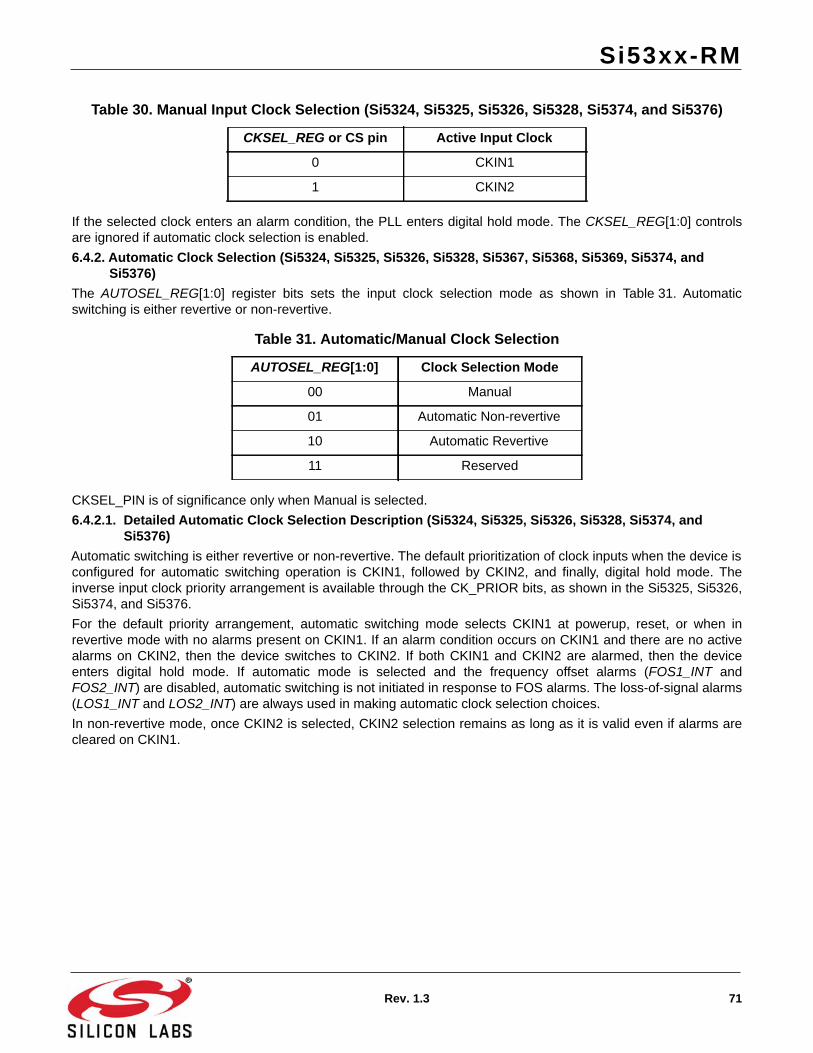
Si53xx-RM
Rev. 1.3 71
If the selected clock enters an alarm condition, the PLL enters digital hold mode. The CKSEL_REG[1:0] controlsare ignored if automatic clock selection is enabled.
6.4.2. Automatic Clock Selection (Si5324, Si5325, Si5326, Si5328, Si5367, Si5368, Si5369, Si5374, and Si5376)
The AUTOSEL_REG[1:0] register bits sets the input clock selection mode as shown in Table 31. Automaticswitching is either revertive or non-revertive.
CKSEL_PIN is of significance only when Manual is selected.
6.4.2.1. Detailed Automatic Clock Selection Description (Si5324, Si5325, Si5326, Si5328, Si5374, and Si5376)
Automatic switching is either revertive or non-revertive. The default prioritization of clock inputs when the device isconfigured for automatic switching operation is CKIN1, followed by CKIN2, and finally, digital hold mode. Theinverse input clock priority arrangement is available through the CK_PRIOR bits, as shown in the Si5325, Si5326,Si5374, and Si5376.
For the default priority arrangement, automatic switching mode selects CKIN1 at powerup, reset, or when inrevertive mode with no alarms present on CKIN1. If an alarm condition occurs on CKIN1 and there are no activealarms on CKIN2, then the device switches to CKIN2. If both CKIN1 and CKIN2 are alarmed, then the deviceenters digital hold mode. If automatic mode is selected and the frequency offset alarms (FOS1_INT andFOS2_INT) are disabled, automatic switching is not initiated in response to FOS alarms. The loss-of-signal alarms(LOS1_INT and LOS2_INT) are always used in making automatic clock selection choices.
In non-revertive mode, once CKIN2 is selected, CKIN2 selection remains as long as it is valid even if alarms arecleared on CKIN1.
Table 30. Manual Input Clock Selection (Si5324, Si5325, Si5326, Si5328, Si5374, and Si5376)
CKSEL_REG or CS pin Active Input Clock
0 CKIN1
1 CKIN2
Table 31. Automatic/Manual Clock Selection
AUTOSEL_REG[1:0] Clock Selection Mode
00 Manual
01 Automatic Non-revertive
10 Automatic Revertive
11 Reserved
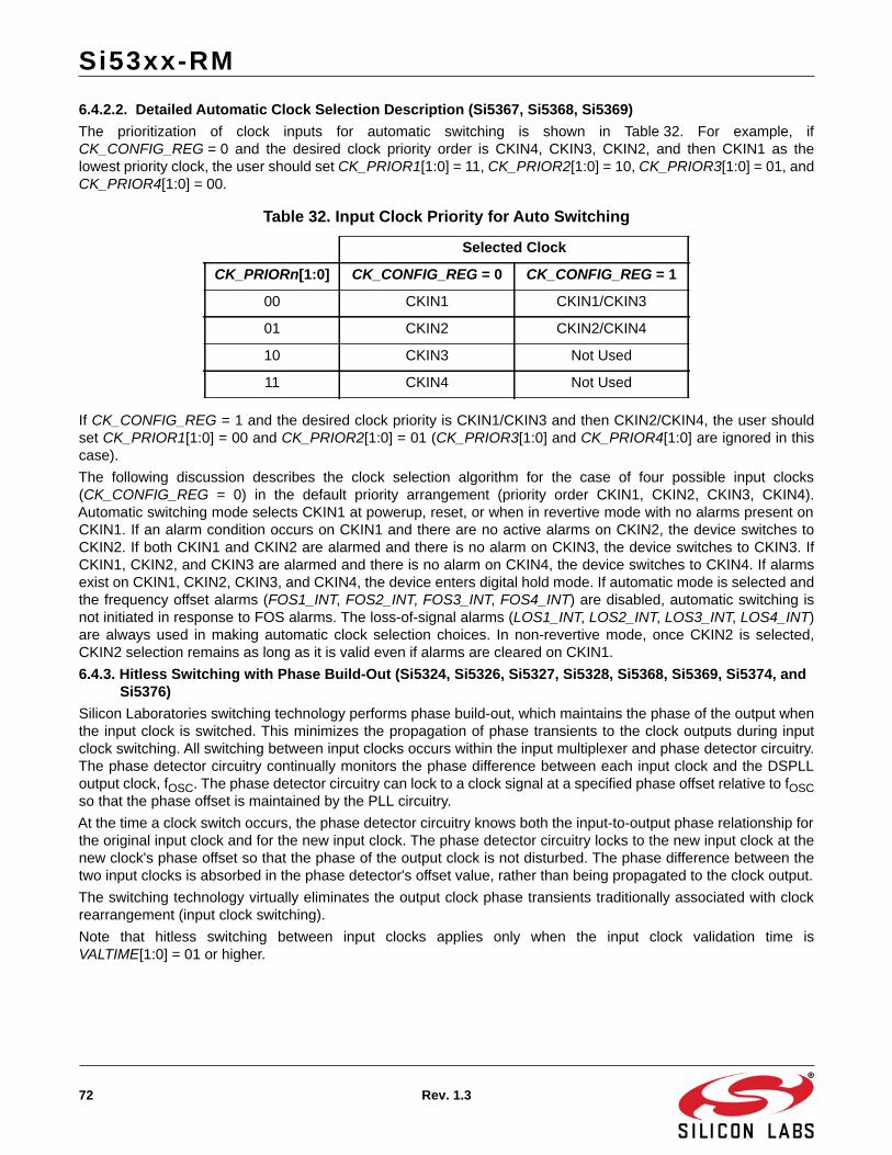
Si53xx-RM
72 Rev. 1.3
6.4.2.2. Detailed Automatic Clock Selection Description (Si5367, Si5368, Si5369)The prioritization of clock inputs for automatic switching is shown in Table 32. For example, ifCK_CONFIG_REG = 0 and the desired clock priority order is CKIN4, CKIN3, CKIN2, and then CKIN1 as thelowest priority clock, the user should set CK_PRIOR1[1:0] = 11, CK_PRIOR2[1:0] = 10, CK_PRIOR3[1:0] = 01, andCK_PRIOR4[1:0] = 00.
If CK_CONFIG_REG = 1 and the desired clock priority is CKIN1/CKIN3 and then CKIN2/CKIN4, the user shouldset CK_PRIOR1[1:0] = 00 and CK_PRIOR2[1:0] = 01 (CK_PRIOR3[1:0] and CK_PRIOR4[1:0] are ignored in thiscase).
The following discussion describes the clock selection algorithm for the case of four possible input clocks(CK_CONFIG_REG = 0) in the default priority arrangement (priority order CKIN1, CKIN2, CKIN3, CKIN4).Automatic switching mode selects CKIN1 at powerup, reset, or when in revertive mode with no alarms present onCKIN1. If an alarm condition occurs on CKIN1 and there are no active alarms on CKIN2, the device switches toCKIN2. If both CKIN1 and CKIN2 are alarmed and there is no alarm on CKIN3, the device switches to CKIN3. IfCKIN1, CKIN2, and CKIN3 are alarmed and there is no alarm on CKIN4, the device switches to CKIN4. If alarmsexist on CKIN1, CKIN2, CKIN3, and CKIN4, the device enters digital hold mode. If automatic mode is selected andthe frequency offset alarms (FOS1_INT, FOS2_INT, FOS3_INT, FOS4_INT) are disabled, automatic switching isnot initiated in response to FOS alarms. The loss-of-signal alarms (LOS1_INT, LOS2_INT, LOS3_INT, LOS4_INT)are always used in making automatic clock selection choices. In non-revertive mode, once CKIN2 is selected,CKIN2 selection remains as long as it is valid even if alarms are cleared on CKIN1.
6.4.3. Hitless Switching with Phase Build-Out (Si5324, Si5326, Si5327, Si5328, Si5368, Si5369, Si5374, and Si5376)
Silicon Laboratories switching technology performs phase build-out, which maintains the phase of the output whenthe input clock is switched. This minimizes the propagation of phase transients to the clock outputs during inputclock switching. All switching between input clocks occurs within the input multiplexer and phase detector circuitry.The phase detector circuitry continually monitors the phase difference between each input clock and the DSPLLoutput clock, fOSC. The phase detector circuitry can lock to a clock signal at a specified phase offset relative to fOSCso that the phase offset is maintained by the PLL circuitry.
At the time a clock switch occurs, the phase detector circuitry knows both the input-to-output phase relationship forthe original input clock and for the new input clock. The phase detector circuitry locks to the new input clock at thenew clock's phase offset so that the phase of the output clock is not disturbed. The phase difference between thetwo input clocks is absorbed in the phase detector's offset value, rather than being propagated to the clock output.
The switching technology virtually eliminates the output clock phase transients traditionally associated with clockrearrangement (input clock switching).
Note that hitless switching between input clocks applies only when the input clock validation time isVALTIME[1:0] = 01 or higher.
Table 32. Input Clock Priority for Auto Switching
Selected Clock
CK_PRIORn[1:0] CK_CONFIG_REG = 0 CK_CONFIG_REG = 1
00 CKIN1 CKIN1/CKIN3
01 CKIN2 CKIN2/CKIN4
10 CKIN3 Not Used
11 CKIN4 Not Used
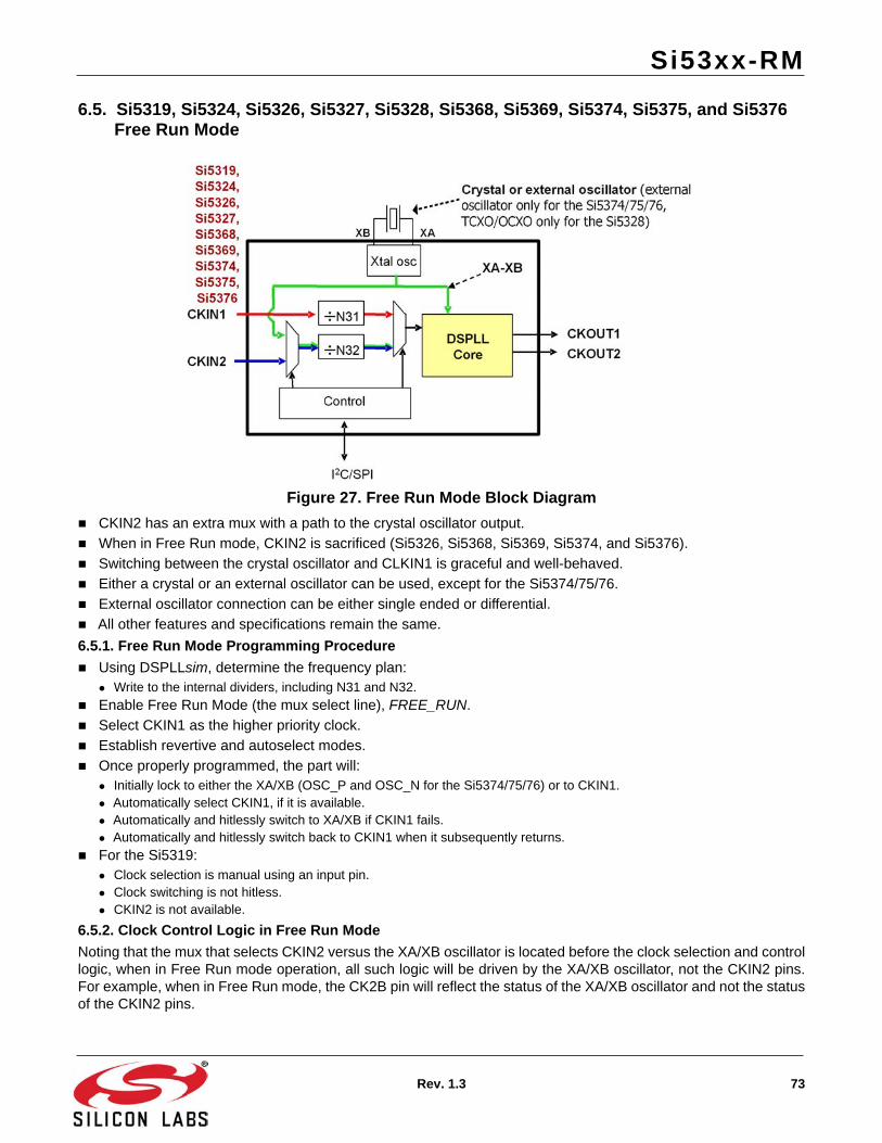
Si53xx-RM
Rev. 1.3 73
6.5. Si5319, Si5324, Si5326, Si5327, Si5328, Si5368, Si5369, Si5374, Si5375, and Si5376 Free Run Mode
Figure 27. Free Run Mode Block Diagram CKIN2 has an extra mux with a path to the crystal oscillator output.
When in Free Run mode, CKIN2 is sacrificed (Si5326, Si5368, Si5369, Si5374, and Si5376).
Switching between the crystal oscillator and CLKIN1 is graceful and well-behaved.
Either a crystal or an external oscillator can be used, except for the Si5374/75/76.
External oscillator connection can be either single ended or differential.
All other features and specifications remain the same.
6.5.1. Free Run Mode Programming Procedure Using DSPLLsim, determine the frequency plan:
Write to the internal dividers, including N31 and N32.
Enable Free Run Mode (the mux select line), FREE_RUN.
Select CKIN1 as the higher priority clock.
Establish revertive and autoselect modes.
Once properly programmed, the part will:Initially lock to either the XA/XB (OSC_P and OSC_N for the Si5374/75/76) or to CKIN1.Automatically select CKIN1, if it is available.Automatically and hitlessly switch to XA/XB if CKIN1 fails.Automatically and hitlessly switch back to CKIN1 when it subsequently returns.
For the Si5319:Clock selection is manual using an input pin.Clock switching is not hitless.CKIN2 is not available.
6.5.2. Clock Control Logic in Free Run ModeNoting that the mux that selects CKIN2 versus the XA/XB oscillator is located before the clock selection and controllogic, when in Free Run mode operation, all such logic will be driven by the XA/XB oscillator, not the CKIN2 pins.For example, when in Free Run mode, the CK2B pin will reflect the status of the XA/XB oscillator and not the statusof the CKIN2 pins.

Si53xx-RM
74 Rev. 1.3
6.5.3. Free Run Reference Frequency Constraints
All crystals and external oscillators must lie within these two bandsNot every crystal will work; they should be testedAn external oscillator can be used at all four bands
The frequency at the phase detector (f3) must be the same for both CKIN1 and XA/XB or else switching cannot be hitless
To avoid spurs, avoid outputs that are an integer (or near integer) of the XA/XB frequency.
6.5.4. Free Run Reference Frequency Constraints While in Free Run:
CKOUT frequency tracks the reference frequency. For very low drift, a TCXO or OCXO reference is necessary.
CKOUT Jitter:XA/XB to CKOUT jitter transfer function is roughly one-to-one.For very low jitter, either use a high quality crystal or external oscillator. 3rd overtone crystals have lower close-in phase noise.In general, higher XA/XB frequency > lower jitter.
XA/XB frequency accuracy:For hitless switching, to meet all published specifications, the XA/XB frequency divided by N32 should match the CLKIN
frequency divided by N31. If they do not match, the clock switch will still be well-behaved.
Other than the above, the absolute accuracy of the XA/XB frequency is not important.
XA/XB Frequency Min XA/XB Frequency Max Xtal
109 MHz 125.5 MHz 3rd overtone
37 MHz 41 MHz Fundamental
CKINN31
--------------- XA-XBN32
------------------ f3= =
CKOUTXA-XB
---------------------- Integer

Si53xx-RM
Rev. 1.3 75
6.6. Digital HoldAll Any-Frequency Precision Clock devices feature a holdover mode, whereby the DSPLL is locked to a digitalvalue.
6.6.1. Narrowband Digital Hold (Si5316, Si5324, Si5326, Si5328, Si5368, Si5369, Si5374, Si5376)After the part's initial self-calibration (ICAL), when no valid input clock is available, the device enters digital hold.Referring to the logical diagram in "Appendix D—Alarm Structure" on page 141, lack of clock availability is definedby following the boolean equation for the Si5324, Si5326, Si5374, and Si5376:
(LOS1_INT OR FOS1_INT) AND (LOS2_INT OR FOS2_INT) = enter digital hold
The equivalent Boolean equation for the Si5327 is as follows:
LOS1 and LOS2 = enter digital hold
The equivalent boolean equation for the Si5367, Si5368, and Si5369 is as follows:
(LOS1_INT OR FOS1_INT) AND (LOS2_INT OR FOS2_INT) AND
(LOS3_INT OR FOS3_INT) AND (LOS4_INT OR FOS4_INT) = enter digital hold
6.6.1.1. Digital Hold Detailed Description (Si5324, Si5326, Si5327, Si5328, Si5368, Si5369, Si5374, and Si5376)
In this mode, the device provides a stable output frequency until the input clock returns and is validated. Uponentering digital hold, the internal DCO is initially held to its last frequency value, M (See Figure 28). Next, the DCOslowly transitions to a historical average frequency value supplied to the DSPLL, MHIST, as shown in Figure 28.Values of M starting from time t = –(HIST_DEL + HIST_AVG) and ending at t = –HIST_DEL are averaged tocompute MHIST. This historical average frequency value is taken from an internal memory location that keeps arecord of previous M values supplied to the DCO. By using a historical average frequency, input clock phase andfrequency transients that may occur immediately preceding digital hold do not affect the digital hold frequency.Also, noise related to input clock jitter or internal PLL jitter is minimized.
Figure 28. Parameters in History Value of MThe history delay can be set via the HIST_DEL[4:0] register bits as shown in Table 33 and the history averagingtime can be set via the HIST_AVG[4:0] register bits as shown in Table 34. The DIGHOLDVALID register can beused to determine if the information in HIST_AVG is valid and the device can enter SONET/SDH compliant digitalhold. If DIGHOLDVALID is not active, the part will enter VCO freeze instead of digital hold.

Si53xx-RM
76 Rev. 1.3
If a highly stable reference, such as an oven-controlled crystal oscillator (OCXO) is supplied at XA/XB, anextremely stable digital hold can be achieved. If a crystal is supplied at the XA/XB port, the digital hold stability willbe limited by the stability of the crystal.
Table 33. Digital Hold History Delay
HIST_DEL[4:0] History Delay Time (ms) HIST_DEL[4:0] History Delay Time (ms)00000 0.0001 10000 6.55
00001 0.0002 10001 13
00010 0.0004 10010 (default) 2600011 0.0008 10011 52
00100 0.0016 10100 105
00101 0.0032 10101 210
00110 0.0064 10110 419
00111 0.01 10111 839
01000 0.03 11000 1678
01001 0.05 11001 3355
01010 0.10 11010 6711
01011 0.20 11011 13422
01100 0.41 11100 26844
01101 0.82 11101 53687
01110 1.64 11110 107374
01111 3.28 11111 214748
Table 34. Digital Hold History Averaging Time
HIST_AVG[4:0] History Averaging Time (ms) HIST_AVG[4:0] History Averaging Time (ms)00000 0.0000 10000 26
00001 0.0004 10001 52
00010 0.001 10010 105
00011 0.003 10011 210
00100 0.006 10100 419
00101 0.012 10101 839
00110 0.03 10110 1678
00111 0.05 10111 3355
01000 0.10 11000 (default) 671101001 0.20 11001 13422
01010 0.41 11010 26844
01011 0.82 11011 53687
01100 1.64 11100 107374
01101 3.28 11101 214748
01110 6.55 11110 429497
01111 13 11111 858993

Si53xx-RM
Rev. 1.3 77
6.6.2. History Settings for Low Bandwidth Devices (Si5324, Si5327, Si5328, Si5369, Si5374)Because of the extraordinarily low loop bandwidth of the Si5324, Si5369 and Si5374, it is recommended that thevalues for both history registers be increased for longer histories.
6.6.3. Recovery from Digital Hold (Si5319, Si5324, Si5326, Si5327, Si5328, Si5368, Si5369, Si5374, and Si5376)
When the input clock signal returns, the device transitions from digital hold to the selected input clock. The deviceperforms hitless recovery from digital hold. The clock transition from digital hold to the returned input clock includes“phase buildout” to absorb the phase difference between the digital hold clock phase and the input clock phase.
6.6.4. VCO Freeze (Si5319, Si5325, Si5367, Si5375)If an LOS or FOS condition exists on the selected input clock, the device enters VCO freeze. In this mode, thedevice provides a stable output frequency until the input clock returns and is validated. When the device entersdigital hold, the internal oscillator is initially held to the frequency value at roughly one second prior to the leadingedge of the alarm condition. VCO freeze is not compliant with SONET/SDH MTIE requirements; applicationsrequiring SONET/SDH MTIE requirements should use the Si5324, Si5326, Si5368, Si5369, Si5374 or Si5376.Unlike the Si5325 and Si5367, the Si5319’s VCO freeze is controlled by the XA/XB reference (which is typically acrystal) resulting in greater stability. For the Si5319, Si5327, and Si5375, VCO freeze is similar to the Digital Holdfunction of the Si5326, Si5368, and Si5369 except that the HIST_AVG and HIST_DEL registers do not exist.
6.6.5. Digital Hold versus VCO FreezeFigure 29 below is an illustration of the difference in behavior between Digital Hold and VCO Freeze.
Figure 29. Digital Hold vs. VCO Freeze Example
Normal operation
Input clock drifts
f0
freq
LOS alarm occurs,
Start Digital hold
Digital Hold
VCO freeze
HIST_AVG HIST_DEL
Clock input cable is pulled
time
~1 sec

Si53xx-RM
78 Rev. 1.3
6.7. Output Phase Adjust (Si5326, Si5368)The device has a highly accurate, digitally controlled device skew capability. For more information on Output PhaseAdjustments, see both DSPLLsim and the respective data sheets. Both can be downloaded by going towww.silabs.com/timing and clicking on “Documentation” at the bottom of the page.
6.7.1. Coarse Skew Control (Si5326, Si5368)With the INCDEC_PIN register bit set to 0 (pin control off), overall device skew is controlled via the CLAT[7:0]register bits. This skew control has a resolution of 1/fOSC, approximately 200 ps, and a range from –25.6 to25.4 ns. Following a powerup or reset (RST pin or RST_REG register bit), the skew will revert to the reset value.Any further changes made in the skew register will be read and compared to the previously held value. Thedifference will be calculated and applied to the clock outputs. All skew changes are made in a glitch-free fashion.
When a phase adjustment is in progress, any new CLAT[7:0] values are ignored until the update is complete. TheCLATPROG register bit is set to 1 during a coarse skew adjustment. The time for an adjustment to complete isdependent on bandwidth and the delta value in CLAT. To verify a written value into CLAT, the CLAT register shouldbe read after the register is written. The time that it takes for the effects of a CLAT change to complete isproportional to the size of the change, at 83 msec for every unit change, assuming the lowest available loopbandwidth was selected. For example, if CLAT is zero and has the value 100 written to it, the changes willcomplete in 100 x 83 msec = 8.3 sec.
If it is necessary to set the high-speed output clock divider N1_HS to divide-by-4 in order to achieve the desiredoverall multiplication ratio and output frequency, only phase increments are allowed and negative settings in theCLAT register or attempts to decrement the phase via writes to the CLAT register will be ignored. Because of thisrestriction, when there is a choice between using N1_HS = 4 and another N1_HS value that can produce thedesired multiplication ratio, the other N1_HS value should be selected. This restriction also applies when using theINC pin.
With the INCDEC_PIN register bit set to 1 (pin control on), the INC and DEC pins function the same as they do forpin controlled parts. See "5.6. Output Phase Adjust (Si5323, Si5366)" on page 58.
6.7.1.1. Unlimited Coarse Skew Adjustment (Si5326, Si5368)Using the following procedure, the CLAT register can be used to adjust the device clock output phase to anarbitrarily large value that is not limited by the size of the CLAT register:
1. Write a phase adjustment value to the CLAT register (Register 16). The DSPLLsim configuration software provides the size of a single step.
2. Wait until CLATPROGRESS = 0 (register 130, bit 7), which indicates that the adjustment is complete (Maximum time for adjustment: 20 seconds for the Si5326 or Si5368).
3. Set INCDEC_PIN = 1 (Register 21, bit 7).
4. Write 0 to CLAT register (Register 16).
5. Wait until CLATPROGRESS = 0.
6. Set INCDEC_PIN = 0.
7. Repeat the above process as many times as desired.
Steps 3-6 will clear the CLAT register without changing the output phase. This allows for unlimited output clockphase adjustment using the CLAT register and repeating steps 1–3 as many times as needed.
Note: The INC and DEC pins must stay low during this process.
6.7.2. Fine Skew Control (Si5326, Si5368)An additional fine adjustment of the overall device skew can be used in conjunction with the INC and DEC pins orthe CLAT[7:0] register bits to provide finer resolution output phase adjustments. Fine phase adjustment is availableusing the FLAT[14:0] bits. The nominal range and resolution of the FLAT[14:0] skew adjustment word are:
Range FLAT = ±110 ps
Resolution FLAT = 9 ps

Si53xx-RM
Rev. 1.3 79
Before writing a new FLAT[14:0] value, the FLAT_VALID bit must be set to 0 to hold the existing FLAT[14:0] valuewhile the new value is being written. Once the new value is written, set FLAT_VALID = 1 to enable its use.
To verify a written value into FLAT, the FLAT register should be read after the register is written.
Because the FLAT resolution varies with the frequency plan and selected bandwidth, DSPLLsim reports the FLATresolution each time it creates a new frequency plan.
6.7.2.1. Output Phase Adjust (Si5324, Si5327, Si5328, Si5369, Si5374)Because of its very low loop bandwidth, the output phase of the Si5324, Si5327, Si5328, Si5369, and Si5374 arenot adjustable. This means that the Si5324, Si5327, Si5328, Si5369, and Si5374 do not have any INC or DEC pinsand that they do not have CLAT or FLAT registers.
6.7.3. Independent Skew (Si5324, Si5326, Si5328, Si5368, Si5369, Si5374, and Si5376)The phase of each clock output may be adjusted in relation to the phase of the other clock outputs, respectively.This feature is available when CK_CONFIG_REG = 0. The resolution of the phase adjustment is equal to [NI HS/FVCO]. Since FVCO is approximately 5 GHz and N1_HS = (4, 5, 6, …, 11), the resolution varies from approximately800 ps to 2.2 ns depending on the PLL divider settings. Silicon Laboratories' PC-based configuration software(DSPLLsim) provides PLL divider settings for each frequency translation, if applicable. If more than one set of PLLdivider settings is available, selecting the combination with the lowest N1_HS value provides the finest resolutionfor output clock phase offset control. The INDEPENDENTSKEWn[7:0] (n = 1 to 5) register bits control the phase ofthe device output clocks. By programming a different phase offset for each output clock, output-to-output delayscan easily be set.
6.7.4. Output-to-output Skew (Si5324, Si5326, Si5327, Si5328, Si5368, Si5369, Si5374, and Si5376)The output-to-output skew is guaranteed to be preserved only if the following two register bits are both high:
Register Bit: LocationCKOUT_ALWAYS_ON addr 0, bit 5
SQICAL addr 3, bit 4
In addition, if SFOUT is changed, the output-to-output skew may be disturbed until after a successful ICAL.
Note: CKOUT5 phase is random unless it is used for Frame Sync (See section 6.8).
6.7.5. Input-to-Output Skew (All Devices)The input-to-output skew for these devices is not controlled.
6.8. Frame Synchronization Realignment (Si5368 and CK_CONFIG_REG = 1)Frame Synchronization Realignment is selected by setting CK_CONFIG_REG = 1. In a typical framesynchronization application, CKIN1 and CKIN2 are high-speed input clocks from primary and secondary clockgeneration cards and CKIN3 and CKIN4 are their associated primary and secondary frame synchronizationsignals. The device generates four output clocks and a frame sync output FS_OUT. CKIN3 and CKIN4 control thephase of FS_OUT. When CK_CONFIG_REG = 1, the Si5368 can lock onto only CKIN1 or CKIN2. CKIN3 andCKIN4 are used only for purposes of frame synchronization.
The inputs supplied to CKIN3 and CKIN4 can range from 2 to 512 kHz. So that two different frame sync inputfrequencies can be accommodated, CKIN3 and CKIN4 each have their own input dividers, as shown in Figure 30.The CKIN3 and CKIN4 frequencies are set by the CKIN3RATE[2:0] and CKIN4RATE[2:0] register bits, as shown inTable 35. The frequency of FS_OUT can range from 2 kHz to 710 MHz and is set using the NC5_LS dividersetting. FS_OUT must divide evenly into CKOUT2. For example, if CKOUT2 is 156.25 MHz, then 8 kHz would notbe an acceptable frame rate because 156.25 MHz/8 kHz = 19,531.25, which is not an integer. However, 2 kHzwould be an acceptable frame rate because 156.25 MHz/2 kHz = 78,125.

Si53xx-RM
80 Rev. 1.3
Figure 30. Frame Sync Frequencies
Table 35. CKIN3/CKIN4 Frequency Selection (CK_CONF = 1)
CKLNnRATE[2:0] CKINn Frequency (kHz) Divisor000 2–4 1
001 4–8 2
010 8–16 4
011 16–32 8
100 32–64 16
101 64–128 32
110 128–256 64
111 256–512 128

Si53xx-RM
Rev. 1.3 81
The NC5_LS divider uses CKOUT2 as its clock input to derive FS_OUT. The limits for the NC5_LS divider are
NC5_LS = [1, 2, 4, 6, …, 219]
fCKOUT2 < 710 MHz
Note that when in frame synchronization realignment mode, writes to NC5_LS are controlled by FPW_VALID. Seesection “6.8.4. FS_OUT Polarity and Pulse Width Control (Si5368)”.
Common NC5_LS divider settings on FS_OUT are shown in Table 36.
6.8.1. FSYNC Realignment (Si5368)The FSYNC_ALIGN_PIN bit determines if the realignment will be pin-controlled via the FS_ALIGN pin or register-controlled via the FSYNC_ALIGN_REG register bit. The active CKIN3 or CKIN4 edge to be used is controlled viathe FSYNC_POL register bit.
In either FSYNC alignment control mode, the resolution of the phase realignment is 1 clock cycle of CKOUT2. Ifthe realignment control is not active, the NC5 divider will continuously divide down its fCKOUT2 input. Thisguarantees a fixed number of high-frequency clock (CKOUT2) cycles between each FS_OUT cycle.
At power-up, the device automatically performs a realignment of FS_OUT using the currently active sync input.After this, as long as the PLL remains in lock and a realignment is not requested, FS_OUT will include a fixednumber of high-speed clock cycles, even if input clock switches are performed. If many clock switches areperformed in phase build-out mode, it is possible that the input sync to output sync phase relationship will shift dueto the accumulated residual phase transients of the phase build-out circuitry. The ALIGN_ERR[8:0] status registerreports the deviation of the input-to-output sync phase skew from the desired FSYNC_SKEW[16:0] value in units offCKOUT2 periods. A programmable threshold to trigger the ALIGN_INT alarm can be set via the ALIGN_THR[2:0]bits, whose settings are given in Table 37. If the sync alignment error exceeds the threshold in either the positive ornegative direction, the alarm becomes active. If it is then desired to reestablish the desired input-to-output syncphase relationship, a realignment can be performed. A realignment request may cause FS_OUT toinstantaneously shift its output edge location in order to align with the active input sync phase.
Table 36. Common NC5 Divider Settings
CKOUT2 Frequency (MHz) NC5 Divider Setting2 kHz FS_OUT 8 kHz FS_OUT
19.44 9720 2430
77.76 38880 9720
155.52 77760 19440
622.08 311040 77760
Table 37. Alignment Alarm Trigger Threshold
ALIGN_THR [2:0] Alarm Trigger Threshold (Units of TCKOUT2)
000 4
001 8
010 16
011 32
100 48
101 64
110 96
111 128

Si53xx-RM
82 Rev. 1.3
For cases where phase skew is required, see Section “6.7. Output Phase Adjust (Si5326, Si5368)” for more detailson controlling the sync input to sync output phase skew via the FSYNC_SKEW[16:0] bits. See Section “7.2. OutputClock Drivers” for information on the FS_OUT signal format, pulse width, and active logic level control.
6.8.2. FSYNC Skew Control (Si5368)When CKIN3 and CKIN4 are configured as frame sync inputs (CK_CONFIG_REG = 1), phase skew of the syncinput active edge to FS_OUT active edge is controllable via the FSYNC_SKEW[16:0] register bits. Skew controlhas a resolution of 1/fCKOUT2 and a range of 131,071/fCKOUT2. The entered skew value must be less than theperiod of CKIN3, CKIN4, and FS_OUT.
The skew should not be changed more than once per FS_OUT period. If a FSYNC realignment is being made, theskew should not be changed until the realignment is complete. The skew value and the FS_OUT pulse widthshould not be changed within the same FS_OUT period.
Before writing the three bytes needed to specify a new FSYNC_SKEW[16:0] value, the user should set the registerbit FSKEW_VALID = 0. This causes the alignment state machine to keep using the previous FSYNC_SKEW[16:0]value, ignoring the new register values as they are being written. Once the new FSYNC_SKEW[16:0] value hasbeen completely written, the user should set FSKEW_VALID = 1 at which time the alignment state machine willread the new skew alignment value. Note that when the new FSYNC_SKEW[16:0] value is used, a phase step willoccur in FS_OUT.
6.8.3. Including FSYNC Inputs in Clock Selection (Si5368)The frame sync inputs, CKIN3 and CKIN4, are both monitored for loss-of-signal (LOS3_INT and LOS4_INT)conditions. To include these LOS alarms in the input clock selection algorithm, set FSYNC_SWTCH_REG = 1. TheLOS3_INT is logically ORed with LOS1_INT and LOS4_INT is ORed with LOS2_INT as inputs to the clockselection state machine. If it is desired not to include these alarms in the clock selection algorithm, setFSYNC_SWTCH_REG = 0. The frequency offset (FOS) alarms for CKIN1 and CKIN2 can also be included in thestate machine decision making as described in Section “6.11. Alarms (Si5319, Si5324, Si5325, Si5326, Si5327,Si5328, Si5367, Si5368, Si5369, Si5374, Si5375, and Si5376)”; however, in frame sync mode(CK_CONFIG_REG = 1), the FOS alarms for CKIN3 and CKIN4 are ignored.
6.8.4. FS_OUT Polarity and Pulse Width Control (Si5368)Additional output controls are available for FS_OUT. The active polarity of FS_OUT is set via the FS_OUT_POLregister bit and the active duty cycle is set via the FSYNC_PW[9:0] register. Pulse width settings have a resolutionof 1/fCKOUT2, and a 50% duty cycle setting is provided. Pulse width settings can range from 1 to (NC5-1) CKOUT2periods, providing the full range of pulse width possibilities for a given NC5 divider setting.
The FS_OUT pulse should not be changed more than once per FS_OUT period. If a FSYNC realignment is beingmade, the pulse width should not be changed until the realignment is complete. The FS_OUT pulse width and theskew value should not be changed within the same FS_OUT period.
Before writing a new value into FSYNC_PW[9:0], the user should set the register bit FPW_VALID = 0. This causesthe FS_OUT pulse width state machine to keep using the previous FSYNC_PW[9:0] value, ignoring the newregister values as they are being written. Once the new FSYNC_PW[9:0] value has been completely written, theuser should set FPW_VALID = 1, at which time the FS_OUT pulse width state machine will read the new pulsewidth value.
Writes to NC5_LS should be treated the same as writes to FSYNC_PW. Thus, all writes to NC5_LS should occuronly when FPW_VALID = 0. Any such writes will not take effect until FPW_VALID = 1.
Note that fCKOUT2 must be less than or equal to 710 MHz when CK_CONFIG_REG = 1; otherwise, the FS_OUTbuffer and NC5 divider must be disabled.
6.8.5. Using FS_OUT as a Fifth Output Clock (Si5368)In applications where the frame synchronization functionality is not needed (CK_CONFIG_REG = 0), FS_OUT canbe used as a fifth clock output. In this case, no realignment requests should be made to the NC5 divider (holdFS_ALIGN = 0 and FSYNC_ALIGN_REG = 0). Output pulse width and polarity controls for FS_OUT are stillavailable as described above. The 50% duty cycle setting would be used to generate a typical balanced outputclock.

Si53xx-RM
Rev. 1.3 83
6.9. Output Clock Drivers (Si5319, Si5324, Si5325, Si5326, Si5327, Si5328, Si5367, Si5368, Si5369, Si5374, Si5375, Si5376)
The device includes a flexible output driver structure that can drive a variety of loads, including LVPECL, LVDS,CML, and CMOS formats. The signal format of each output is individually configurable through theSFOUTn_REG[2:0] register bits, which modify the output common mode and differential signal swing.
Table 38 shows the signal formats based on the supply voltage and the type of load being driven. For the CMOSsetting, both output pins drive single-ended in-phase signals and should be externally shorted together to obtainthe maximum drive strength.
The SFOUTn_REG[2:0] register bits can also be used to disable the outputs. Disabling the outputs puts theCKOUT+ and CKOUT– pins in a high-impedance state relative to VDD (common mode tri-state) while the twooutputs remain connected to each other through a 200 on-chip resistance (differential impedance of 200 ). Theclock output buffers and DSPLL output dividers NCn are powered down in disable mode.
The additional functions of “Hold Logic 1” and “Hold Logic 0”, which create static logic levels at the outputs, areavailable. For differential output buffer formats, the Hold Logic 1 state causes the positive output of the differentialsignal to remain at its high logic level while the negative output remains at the low logic level. For CMOS outputbuffer format, both outputs remain high during the Hold Logic 1 state. These functions are controlled by theHLOG_n bits. When entering or exiting the “Hold Logic 1” or “Hold Logic 0” states, no glitches or runt pulses aregenerated on the outputs. Changes to SFOUT or HLOG will change the output phase. An ICAL is required to re-establish the output phase. When SFOUT = 010 for CMOS, bypass mode is not supported.
6.9.1. Disabling CKOUTnDisabling CKOUTn output powers down the output buffer and output divider. Individual disable controls areavailable for each output using the DSBLn_REG.
6.9.2. LVPECL TQFP Output Signal Format Restrictions at 3.3 V (Si5367, Si5368, Si5369)The LVPECL and CMOS output formats draw more current than either LVDS or CML; therefore, there arerestrictions in the allowed output format pin settings that limit the maximum power dissipation for the TQFP deviceswhen they are operated at 3.3 V. When Vdd = 3.3 V and there are four enabled LVPECL or CMOS outputs, the fifthoutput must be disabled. When Vdd = 3.3 V and there are five enabled outputs, there can be no more than threeoutputs that are either LVPECL or CMOS. All other configurations are valid, including all with Vdd = 2.5 V.
Table 38. Output Signal Format Selection
SFOUTn_REG[2:0] Signal Format
111 LVDS
110 CML
101 LVPECL
011 Low-swing LVDS
010 CMOS
000 Disabled
All Others Reserved

Si53xx-RM
84 Rev. 1.3
6.10. PLL Bypass Mode (Si5319, Si5324, Si5325, Si5326, Si5327, Si5328, Si5367, Si5368, Si5369, Si5374, Si5375, and Si5376)
The device supports a PLL bypass mode in which the selected input clock is fed directly to the output buffers,bypassing the DSPLL. In PLL bypass mode, the input and output clocks will be at the same frequency. PLL bypassmode is useful in a laboratory environment to measure system performance with and without the jitter attenuationprovided by the DSPLL. The BYPASS_REG bit controls enabling/disabling PLL bypass mode.
Before going into bypass mode, it is recommended that the part enter Digital Hold by setting DHOLD. Internally, thebypass path is implemented with high-speed differential signaling for low jitter. Note that the CMOS output formatdoes not support bypass mode.
6.11. Alarms (Si5319, Si5324, Si5325, Si5326, Si5327, Si5328, Si5367, Si5368, Si5369, Si5374, Si5375, and Si5376)
Summary alarms are available to indicate the overall status of the input signals and frame alignment (Si5368 only).Alarm outputs stay high until all the alarm conditions for that alarm output are cleared. The Register VALTIMEcontrols how long a valid signal is re-applied before an alarm clears. Table 39 shows the available settings. Notethat only for VALTIME[1:0] = 00, hitless switching is not possible.
6.11.1. Loss-of-Signal Alarms (Si5319, Si5324, Si5325, Si5326, Si5327, Si5328, Si5367, Si5368, Si5369, Si5374, Si5375, and Si5376)
The device has loss-of-signal circuitry that continuously monitors CKINn for missing pulses. The LOS circuitrygenerates an internal LOSn_INT output signal that is processed with other alarms to generate CnB andALARMOUT.
An LOS condition on CKIN1 causes the internal LOS1_INT alarm become active. Similarly, an LOS condition onCKINn causes the LOSn_INT alarm become active. Once a LOSn_INT alarm is asserted on one of the inputclocks, it remains asserted until that input clock is validated over a designated time period. If another errorcondition on the same input clock is detected during the validation time then the alarm remains asserted and thevalidation time starts over.
6.11.1.1. Narrowband LOS Algorithms (Si5319, Si5324, Si5326, Si5327, Si5328, Si5368, Si5369, Si5374, Si5375, and Si5376)
There are three options for LOS: LOS, LOS_A, and no LOS, which are selected using the LOSn_EN registers. Thevalues for the LOSn_EN registers are given in Table 40.
Table 39. Loss-of-Signal Validation Times
VALTIME[1:0] Clock Validation Time
00 2 ms (hitless switching not available)
01 100 ms
10 200 ms
11 13 s
Table 40. Loss-of-Signal Registers
LOSn_EN[1:0] LOS Selection
00 Disable all LOS monitoring
01 Reserved
10 LOS_A enabled
11 LOS enabled

Si53xx-RM
Rev. 1.3 85
6.11.1.2. Standard LOS (Si5319, Si5324, Si5326, Si5327, Si5328, Si5368, Si5369, Si5374, Si5375, and Si5376)To facilitate automatic hitless switching, the LOS trigger time can be significantly reduced by using the default LOSoption (LOSn_EN = 11). The LOS circuitry divides down each input clock to produce a 2 kHz to 2 MHz signal. TheLOS circuitry over samples this divided down input clock using a 40 MHz clock to search for extended periods oftime without input clock transitions. If the LOS monitor detects twice the normal number of samples without a clockedge, an LOS alarm is declared. The LOSn trigger window is based on the value of the input divider N3. The valueof N3 is reported by DSPLLsim.
The range over which LOS is guaranteed to not produce false positive assertions is 100 ppm. For example, if adevice is locked to an input clock on CKIN1, the frequency of CKIN2 should differ by no more than 100 ppm toavoid false LOS2 assertions.
The frequency range over which FOS monitoring may occur is from 10 to 710 MHz.
6.11.1.3. LOSA (Si5319, Si5324, Si5326, Si5327, Si5328, Si5368, Si5369, Si5374, Si5375, and Si5376)A slower response version of LOS called LOSA is available and should be used under certain conditions. BecauseLOSA is slower and less sensitive than LOS, its use should be considered for applications with quasi-periodicclocks (e.g., gapped clocks with one or more consecutive clock edges removed), when switching between inputclocks with a large difference in frequency and any other application where false positive assertions of LOS mayincorrectly cause the Any-Frequency device to be forced into Digital Hold.
For example, one might consider the use of LOSA instead of LOS in Free Run mode applications because the twoclock inputs will not be the same exact frequency. This will avoid false LOS assertions when the XA/XB frequencydiffers from the other clock inputs by more than 100 ppm. See Section 6.11.1.3 for more information on LOSA.
6.11.1.4. LOS disabled (Si5319, Si5324, Si5326, Si5327, Si5328, Si5368, Si5369, Si5374, Si5375, and Si5376)For situations where no form of LOS is desired, LOS can be disabled by writing 00 to LOSn_EN. This mode isprovided to support applications which implement custom LOS algorithms off-chip. If this approach is taken, theonly remaining methods of entering Digital Hold will be FOS or by setting DHOLD (register 3, bit 5).
6.11.1.5. Wideband LOS Algorithm (Si5322, Si5365)Each input clock is divided down to produce a 78 kHz to 1.2 MHz signal before entering the LOS monitoringcircuitry. The same LOS algorithm as described in the above section is then used. FOS is not available in widebanddevices.
6.11.1.6. LOS Alarm Outputs (Si5319, Si5324, Si5325, Si5326, Si5327, Si5328, Si5367, Si5369, Si5374, Si5375, and Si5376)
When LOS is enabled, an LOS condition on CKIN1 causes LOS1_INT to become active. Similarly, when LOS isenabled, an LOS condition on CKIN2 causes LOS2_INT to become active. Once a LOSn_INT alarm is asserted onone of the input clocks, it remains asserted until the input clock is validated over a designated time period. Ifanother error condition on the same input clock is detected during the validation time then the alarm remainsasserted and the validation time starts over.
6.11.2. FOS Algorithm (Si5324, Si5325, Si5326, Si5328, Si5368, Si5369, Si5374, and Si5376)The frequency offset (FOS) alarms indicate if the input clocks are within a specified frequency range relative to thefrequency of a reference clock. The reference clock can be provided by any of the four input clocks (two for Si5324,Si5325 or Si5326) or the XA/XB input. The default FOS reference is CKIN2. The frequency monitoring circuitrycompares the frequency of the input clock(s) with the FOS reference clock If the frequency offset of an input clockexceeds a selected frequency offset threshold, an FOS alarm (FOS_INT register bit) is declared for that clockinput. Be aware that large amounts of wander can cause false FOS alarms.
Note: For the Si5368, If CK_CONFIG_REG = 1, only CKIN1 and CKIN2 are monitored; CKIN3 and CKIN4 are used forFSYNC and are not monitored.
The frequency offset threshold is selectable using the FOS_THR[1:0] bits. Settings are available for compatibilitywith SONET Minimum Clock (SCMD) or Stratum 3/3E requirements. See the data sheet for more information. Thedevice supports FOS hystereses per GR-1244-CORE, making the device less susceptible to FOS alarmchattering. A reference clock with suitable accuracy and drift specifications to support the intended applicationshould be used. The FOS reference clock is set via the FOSREFSEL[2:0] bits as shown in Table 41. More than oneinput can be monitored against the FOS reference, i.e., there can be more than one monitored clock, but only one

Si53xx-RM
86 Rev. 1.3
FOS reference. When the XA/XB input is used as the FOS reference, there is only one reference frequency bandthat is allowed: from 37 MHz to 41 MHz.
Both the FOS reference and the FOS monitored clock must be divided down to the same clock rate and this clockrate must be between 10 MHz and 27 MHz. As can be seen in Figure 31, the values for P and Q must be selectedso that the FOS comparison occurs at the same frequency. The registers that contain the values for P and Q arethe CKINnRATE[2:0] registers.
Figure 31. FOS CompareThe frequency band of each input clock must be specified to use the FOS feature. The CLKNRATE registersspecify the frequency of the device input clocks as shown in Table 42.
When the FOS reference is the XA/XB oscillator (either internal or external), the value of Q in Figure 31 is always2, for an effective CLKINnRATE of 1, as shown in Table 42.
Table 41. FOS Reference Clock Selection
FOS ReferenceFOSREFSEL[2:0] Si5326 Si5368
000 XA/XB XA/XB
001 CKIN1 CKIN1
010 CKIN2 (default) CKIN2 (default)
011 Reserved CKIN3
100 Reserved CKIN4
all others Reserved Reserved
Table 42. CLKnRATE Registers
CLKnRATE Divisor, P or Q Min Frequency, MHz Max Frequency, MHz
0 1 10 27
1 2 25 54
2 4 50 105
3 8 95 215
4 16 190 435
5 32 375 710

Si53xx-RM
Rev. 1.3 87
For example, to monitor a 544 MHz clock at CKIN1 with a FOS reference of 34 MHz at CKIN2:
CLK1RATE = 5
CLK2RATE = 1
FOSREFSEL[2:0] = 010
6.11.3. C1B, C2B (Si5319, Si5324, Si5325, Si5326, Si5327, Si5328, Si5374, Si5375, and Si5376)A LOS condition causes the associated LOS1_INT or LOS2_INT read only register bit to be set. A LOS conditionon CKIN_1 will also be reflected onto C1B if CK1_BAD_PIN = 1. Likewise, a LOS condition on CKIN_2 will also bereflected onto C2B if CK2_BAD_PIN = 1.
A FOS condition causes the associated FOS1_INT or FOS2_INT read only register bit to be set. FOS monitoring isenabled or disabled using the FOS_EN bit. If FOS is enabled (FOS_EN = 1) and CK1_BAD_PIN = 1, a FOScondition will also be reflected onto its associated output pin, C1B or C2B. If FOS is disabled (FOS_EN = 0), theFOS1_INT and FOS2_INT register bits do not affect the C1B and C2B alarm outputs, respectively.
Once an LOS or FOS alarm is asserted on one of the input clocks, it is held high until the input clock is validatedover a designated time period. The validation time is programmable via the VALTIME[1:0] register bits as shown inTable 39 on page 84. If another error condition on the same input clock is detected during the validation time thenthe alarm remains asserted and the validation time starts over.
[Si5326]: Note that hitless switching between input clocks applies only when the input clock validation timeVALTIME[1:0] = 01 or higher.
6.11.4. LOS (Si5319, Si5375)A LOS condition causes the LOS_INT read only register bit to be set. This LOS condition will also be reflected ontothe INT_CB pin.
6.11.5. C1B, C2B, C3B, ALRMOUT (Si5367, Si5368, Si5369 [CK_CONFIG_REG = 0])The generation of alarms on the C1B, C2B, C3B, and ALRMOUT outputs is a function of the input clockconfiguration, and the frequency offset alarm enable as shown in Table 43. The LOSn_INT and FOSn_INT signalsare the raw outputs of the alarm monitors. These appear directly in the device status registers. Sticky versions ofthese bits (LOSn_FLG, FOSn_FLG) drive the output interrupt and can be individually masked. When the deviceinputs are configured as four input clocks (CK_CONFIG = 0), the ALRMOUT pin reflects the status of the CKIN4input. The equations below assume that the output alarm is active high; however, the active polarity is selectablevia the CK_BAD_POL bit.
Operation of the C1B, C2B, C3B, and ALRMOUT pins is enabled based on setting the C1B_PIN, C2B_PIN,C3B_PIN, and ALRMOUT_PIN register bits. Otherwise, the pin will tri-state. Also, if INT_PIN = 1, the interruptfunctionality will override the appearance of ALRMOUT at the output even if ALRMOUT_PIN = 1.
Once an LOS or FOS alarm is asserted for one of the input clocks, it is held high until the input clock is validatedover a designated time period. The validation time is programmable via the VALTIME[1:0] register bits as shown inTable 39 on page 84. If another error condition on the same input clock is detected during the validation time thenthe alarm remains asserted and the validation time starts over.
Note that hitless switching between input clocks applies only when the input clock validation timeVALTIME[1:0] = 01 or higher.
For details, see "Appendix D—Alarm Structure" on page 141.

Si53xx-RM
88 Rev. 1.3
6.11.6. C1B, C2B, C3B, ALRMOUT (Si5368 [CK_CONFIG_REG = 1])The generation of alarms on the C1B, C2B, C3B, and ALRMOUT outputs is a function of the input clockconfiguration, and the frequency offset alarm enable as shown in Table 44. The LOSn_INT and FOSn_INT signalsare the raw outputs of the alarm monitors. These appear directly in the device status registers. Sticky versions ofthese bits (LOSn_FLG, FOSn_FLG) drive the output interrupt and can be individually masked. Since, CKIN3 andCKIN4 are configured as frame sync inputs (CK_CONFIG_REG = 1), ALRMOUT functions as the alignment alarmoutput (ALIGN_INT) as described in Section “6.8. Frame Synchronization Realignment (Si5368 andCK_CONFIG_REG = 1)”. The equations below assume that the output alarm is active high; however, the activepolarity is selectable via the CK_BAD_POL bit.
Operation of the C1B, C2B, C3B, and ALRMOUT pins is enabled based on setting the C1B_PIN, C2B_PIN,C3B_PIN, and ALRMOUT_PIN register bits. Otherwise, the pin will tri-state. Also, if INT_PIN = 1, the interruptfunctionality will override the appearance of ALRMOUT at the output even if ALRMOUT_PIN = 1.
Once an LOS or FOS alarm is asserted for one of the input clocks, it is held high until the input clock is validatedover a designated time period. The validation time is programmable via the VALTIME[1:0] register bits as describedin the data sheet. If another error condition on the same input clock is detected during the validation time then thealarm remains asserted and the validation time starts over.
Note that hitless switching between input clocks applies only when the input clock validation timeVALTIME[1:0] = 01 or higher.
Table 43. Alarm Output Logic Equations (Si5367, Si5368, and Si5369 [CONFIG_REG = 0])
FOS_EN Alarm Output Equations
0(Disables FOS)
C1B = LOS1_INTC2B = LOS2_INTC3B = LOS3_INT
ALRMOUT = LOS4_INT
1 C1B = LOS1_INT or FOS1_INTC2B = LOS2_INT or FOS2_INTC3B = LOS3_INT or FOS3_INT
ALRMOUT = LOS4_INT or FOS4_INT
Table 44. Alarm Output Logic Equations [Si5368 and CKCONFIG_REG = 1]
FOS_EN Alarm Output Equations
0(Disables FOS)
C1B = LOS1_INT or (LOS3_INT and FSYNC_SWTCH_REG)C2B = LOS2_INT or (LOS4_INT and FSYNC_SWTCH_REG)
C3B tri-state, ALRMOUT = ALIGN_INT
1 C1B = LOS1_INT or (LOS3_INT and FSYNC_SWTCH_REG) or FOS-1_INT
C2B = LOS2_INT or (LOS4_INT and FSYNC_SWTCH_REG) or FOS-2_INT
C3B tri-state, ALRMOUT = ALIGN_INT

Si53xx-RM
Rev. 1.3 89
6.11.7. LOS Algorithm for Reference Clock Input (Si5319, Si5324, Si5326, Si5327, Si5328, Si5368, Si5369, Si5374, Si5375, and Si5376)
The reference clock input on the XA/XB port is monitored for LOS. The LOS circuitry divides the signal at XA/XB by128, producing a 78 kHz to 1.2 MHz signal, and monitors the signal for LOS using the same algorithm as describedin Section “6.11.1. Loss-of-Signal Alarms (Si5319, Si5324, Si5325, Si5326, Si5327, Si5328, Si5367, Si5368,Si5369, Si5374, Si5375, and Si5376)”. The LOSX_INT read only bit reflects the state of a loss-of-signal monitor onthe XA/XB port. For the Si5374, Si5375, and Si5376, the XA/XB port refers to the OSC_P and OSC_N pins.
6.11.8. LOL (Si5319, Si5324, Si5326, Si5327, Si5328, Si5368, Si5369, Si5374, Si5375, and Si5376)The device has a PLL lock detection algorithm that indicates the lock status on the LOL output pin and theLOL_INT read-only register bit. The algorithm works by continuously monitoring the phase of the input clock inrelation to the phase of the feedback clock. A retriggerable one-shot is set each time a potential phase cycle slipcondition is detected. If no potential phase cycle slip occurs for the retrigger time, the LOL output is set low,indicating the PLL is in lock. The LOL pin is held in the active state during an internal PLL calibration. The activepolarity of the LOL output pin is set using the LOL_POL register bit (default active high).
The lock detect retrigger time is user-selectable, independent of the loop bandwidth. The LOCKT[2:0] register bitsmust be set by the user to the desired setting. Table 45 shows the lock detect retrigger time for both modes ofoperation. LOCKT is the minimum amount of time that LOL will be active.
6.11.9. Device InterruptsAlarms on internal real-time status bits such as LOS1_INT, FOS1_INT, etc. cause their associated interrupt flags(LOS1_FLG, FOS1_FLG, etc.) to be set and held. The interrupt flag bits can be individually masked or unmaskedwith respect to the output interrupt pin. Once an interrupt flag bit is set, it will remain high until the register locationis written with a “0” to clear the flag.
6.12. Device ResetUpon powerup or asserting Reset via the RST pin or software, the device internally executes a power-on-reset(POR) which resets the internal device logic and tristates the device outputs. The device waits for configurationcommands and the receipt of the ICAL = 1 command to start its calibration. Any changes to the CMODE pinrequire that RST be toggled to reset the part. The power-up default register values are given in the data sheets forthese parts.
Table 45. Lock Detect Retrigger Time (LOCKT)
LOCKT[2:0] Retrigger Time (ms)
000 106
001 53
010 26.5
011 13.3
100 6.6 (value after reset)
101 3.3
110 1.66
111 .833

Si53xx-RM
90 Rev. 1.3
6.13. I2C Serial Microprocessor InterfaceWhen configured in I2C control mode (CMODE = L), the control interface to the device is a 2-wire bus forbidirectional communication. The bus consists of a bidirectional serial data line (SDA) and a serial clock input(SCL). Both lines must be connected to the positive supply via an external pull-up. In addition, an output interrupt(INT) is provided with selectable active polarity (determined by INT_POL bit). Fast mode operation is supported fortransfer rates up to 400 kbps as specified in the I2C-Bus Specification standard. To provide bus address flexibility,three pins (A[2:0]) are available to customize the LSBs of the device address. The complete bus address for thedevice is as follows:
1 1 0 1 A[2] A[1] A[0] R/W.
Figure 32 shows the command format for both read and write access. Data is always sent MSB first. The timingspecifications and timing diagram for the I2C bus can be found in the I2C-Bus Specification standard (fast modeoperation) (See: http://www.standardics.nxp.com/literature/books/i2c/pdf/i2c.bus.specification.pdf).
The maximum I2C clock speed is 400 kHz.
Figure 32. I2C Command FormatIn Figure 33, the value 68 is seven bits. The sequence of the example is: Write register 00 with the value 0xAA;then, read register 00. Note that 0 = Write = W, and 1 = Read = R.
Figure 33. I2C Example

Si53xx-RM
Rev. 1.3 91
6.14. Serial Microprocessor Interface (SPI)When configured in SPI control mode (CMODE = H), the control interface to the device is a 4-wire interfacemodeled after commonly available microcontroller and serial peripheral devices. The interface consists of a clockinput (SCLK), slave select input (SSb), serial data input (SDI), and serial data output (SDO). In addition, an outputinterrupt (INT) is provided with selectable active polarity (determined by INT_POL bit).
Data is transferred a byte at a time with each register access consisting of a pair of byte transfers. Figure 34 andFigure 35 illustrate read and write/set address operations on the SPI bus, and AC SPEC gives the timingrequirements for the interface. Table 46 shows the SPI command format.
The first byte of the pair is the instruction byte. The “Set Address” command writes the 8 bit address value that willbe used for the subsequent read or write. The “Write” command writes data into the device based on the addresspreviously established and the “Write/Address Increment” command writes data into the device and thenautomatically increments the register address for use on the subsequent command. The “Read” command readsone byte of data from the device and the “Read/Address Increment” reads one byte and increments the registeraddress automatically. The second byte of the pair is the address or data byte.
As shown in Figure 34 and Figure 35, SSb should be held low during the entire two byte transfer. Raising SSbresets the internal state machine; so, SSb can optionally be raised between each two byte transfers to guaranteethe state machine will be reinitialized. During a read operation, the SDO becomes active on the falling edge ofSCLK and the 8-bit contents of the register are driven out MSB first. The SDO is high impedance on the rising edgeof SS. SDI is a “don’t care” during the data portion of read operations. During write operations, data is driven intothe device via the SDI pin MSB first. The SDO pin will remain high impedance during write operations. Data alwaystransitions with the falling edge of the clock and is latched on the rising edge. The clock should return to a logichigh when no transfer is in progress.
The SPI port supports continuous clocking operation where SSb is used to gate two or four byte transfers. Themaximum speed supported by SPI is 10 MHz.
Table 46. SPI Command Format
Instruction(BYTE0) Address/Data[7:0](BYTE1)
00000000—Set Address AAAAAAAA
01000000—Write DDDDDDDD
01100000—Write/Address Increment DDDDDDDD
10000000—Read DDDDDDDD
10100000—Read/Address Increment DDDDDDDD

Si53xx-RM
92 Rev. 1.3
Figure 34. SPI Write/Set Address Command
Figure 35. SPI Read CommandFigure 35 shows the SPI timing diagram. See the applicable data sheets for these timing parameters.

Si53xx-RM
Rev. 1.3 93
Figure 36. SPI Timing Diagram
6.14.1. Default Device ConfigurationFor ease of manufacture and bench testing of the device, the default register settings have been chosen to placethe device in a fully-functional mode with an easily-observable output clock. Refer to the data sheet for your device.
6.15. Register DescriptionsSee the device data sheet for a full description of the registers.
6.16. DSPLLsim Configuration SoftwareTo simplify frequency planning, loop bandwidth selection, and general device configuration, of the Any-FrequencyPrecision Clocks. Silicon Laboratories has a configuration utility - DSPLLsim for the Si5319, Si5325, Si5326,Si5327, Si5328, Si5367, Si5368 and Si5369. For the Si5374, Si5375, and Si5376, there is a different configurationutility - Si537xDSPLLsim. Both are available to download from www.silabs.com/timing.

Si53xx-RM
94 Rev. 1.3
7. High-Speed I/O7.1. Input Clock BuffersAny-Frequency Precision Clock devices provide differential inputs for the CKINn clock inputs. These inputs areinternally biased to a common mode voltage and can be driven by either a single-ended or differential source.Figure 37 through Figure 41 show typical interface circuits for LVPECL, CML, LVDS, or CMOS input clocks. Notethat the jitter generation improves for higher levels on CKINn (within the limits described in the data sheet).
AC coupling the input clocks is recommended because it removes any issue with common mode input voltages.However, either ac or dc coupling is acceptable. Figures 37 and 38 show various examples of different inputtermination arrangements.
Unused inputs should have an ac ground connection. For microprocessor-controlled devices, the PD_CKn bitsmay be set to shut off unused input buffers to reduce power.
Figure 37. Differential LVPECL Termination
Figure 38. Single-Ended LVPECL Termination

Si53xx-RM
Rev. 1.3 95
Figure 39. CML/LVDS Termination (1.8, 2.5, 3.3 V)
Figure 40. Center Tap Bypassed TerminationFigure 40 is recommended over a single 100 resistor whenever greater reduction of common-mode noise isdesired. It can be used with any differential termination, either input or output.
Figure 41. CMOS Termination (1.8, 2.5, 3.3 V)

Si53xx-RM
96 Rev. 1.3
7.2. Output Clock DriversThe output clocks can be configured to be compatible with LVPECL, CML, LVDS, or CMOS as shown in Table 47.
Unused outputs can be left unconnected. For microprocessor-controlled devices, it is recommended to write“disable” to SFOUTn to disable the output buffer and reduce power. When the output mode is CMOS, bypassmode is not supported.
7.2.1. LVPECL TQFP Output Signal Format Restrictions at 3.3 V (Si5367, Si5368, Si5369)The LVPECL and CMOS output formats draw more current than either LVDS or CML; however, there arerestrictions in the allowed output format pin settings so that the maximum power dissipation for the TQFP devicesis limited when they are operated at 3.3 V. When Vdd = 3.3 V and there are four enabled LVPECL or CMOSoutputs, the fifth output must be disabled. When Vdd = 3.3 V and there are five enabled outputs, there can be nomore than three outputs that are either LVPECL or CMOS. All other configurations are valid, including those withVdd = 2.5 V.
7.2.2. Typical Output CircuitsIt is recommended that the outputs be ac coupled to avoid common mode issues. This suggestion does not applyto the Si5366 and Si5368 when CKOUT5 is configured as FS_OUT (frame sync) because it can a have a dutycycle significantly different from 50%.
Figure 42. Typical Output Circuit (Differential)
Table 47. Output Driver Configuration
Output Mode SFOUTn Pin Settings(Si5316, Si5322, Si5323, Si5365)
SFOUTn_REG [2:0] Settings(Si5319, Si5325, SI5326, Si5327, Si5328, Si5367, Si5368, Si5369,
Si5374, Si5375, and Si5376)
LVDS HM 111
CML HL 110
LVPECL MH 101
Low-swing LVDS
ML 011
CMOS LH 010
Disabled LM 000
Reserved All Others All Others
Note: The LVPECL outputs are “LVPECL compatible.” No DC biasing circuitry is required to drive a standard LVPECL load.

Si53xx-RM
Rev. 1.3 97
Figure 43. Differential Output Example Requiring Attenuation
Figure 44. Typical CMOS Output Circuit (Tie CKOUTn+ and CKOUTn– Together)Unused output drivers should be powered down, per Table 48, or left floating.
The pin-controlled parts have a DBL2_BY pin that can be used to disable CKOUT2.
Table 48. Disabling Unused Output Driver
Output Driver Si5365, Si5366 Si5325, Si5326, Si5327, Si5328, Si5367, Si5368
CKOUT1 and CKOUT2 N/A Use SFOUT_REG to disable individ-ual CKOUTn.CKOUT3 and CKOUT4 DBL34
CKOUT5/FS_OUT DBL5/DBL_FS

Si53xx-RM
98 Rev. 1.3
Figure 45. Differential CKOUT Structure (not for CMOS)
7.2.3. Typical Clock Output Scope Shots
Table 49. Output Format Measurements1,2
Name SFOUT Pin SFOUT Code SingleVpk–pk
DiffVpk–pk
Vocm
Reserved HH — — — —
LVDS HM 7 .35 .7 1.2
CML HLK 6 .25 .5 3.05
LVPECL MH 5 .75 1.5 2.10
Reserved MM 4 — — —
Low Swing LVDS ML 3 .25 .5 1.2
CMOS LH 2 3.3 — 1.65
Disable LM 1 — — —
Reserved LL 0 — — —
Notes:1. Typical measurements with an Si5326 at VC = 3.3 V.2. For all measurements:
Vpk-pk on a single output, double the values for differential.Vdd = 3.3 V.50 ac load to ground.

Si53xx-RM
Rev. 1.3 99
7.3. Typical Scope Shots for SFOUT Options
Figure 46. sfout_2, CMOS
Figure 47. sfout_3, lowSwingLVDS

Si53xx-RM
100 Rev. 1.3
Figure 48. sfout_5, LVPECL
Figure 49. sfout_6, CML

Si53xx-RM
Rev. 1.3 101
Figure 50. sfout_7, LVDS
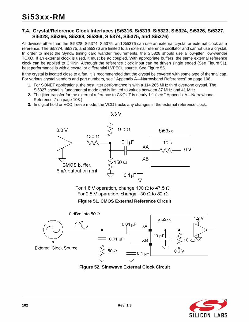
Si53xx-RM
102 Rev. 1.3
7.4. Crystal/Reference Clock Interfaces (Si5316, Si5319, Si5323, Si5324, Si5326, Si5327, Si5328, Si5366, Si5368, Si5369, Si5374, Si5375, and Si5376)
All devices other than the Si5328, Si5374, Si5375, and Si5376 can use an external crystal or external clock as areference. The Si5374, Si5375, and Si5376 are limited to an external reference oscillator and cannot use a crystal.In order to meet the SyncE timing card wander requirements, the Si5328 should use a low-jitter, low-wanderTCXO. If an external clock is used, it must be ac coupled. With appropriate buffers, the same external referenceclock can be applied to CKINn. Although the reference clock input can be driven single ended (See Figure 51),best performance is with a crystal or differential LVPECL source. See Figure 55.
If the crystal is located close to a fan, it is recommended that the crystal be covered with some type of thermal cap.For various crystal vendors and part numbers, see " Appendix A—Narrowband References" on page 108.
1. For SONET applications, the best jitter performance is with a 114.285 MHz third overtone crystal. The Si5327 crystal is fundamental mode and is limited to values between 37 MHz and 41 MHz.
2. The jitter transfer for the external reference to CKOUT is nearly 1:1 (see " Appendix A—Narrowband References" on page 108.)
3. In digital hold or VCO freeze mode, the VCO tracks any changes in the external reference clock.
Figure 51. CMOS External Reference Circuit
Figure 52. Sinewave External Clock Circuit

Si53xx-RM
Rev. 1.3 103
Figure 53. Differential External Reference Input Example(Not for Si5374, Si5375, or Si5376)
Figure 54. Differential OSC Reference Input Example for Si5374, Si5375 and Si5376

Si53xx-RM
104 Rev. 1.3
7.5. Three-Level (3L) Input Pins (No External Resistors)
Figure 55. Three Level Input Pins
Parameter Symbol Min Max
Input Voltage Low Vill — .15 x VDD
Input Voltage Mid Vimm .45 x Vdd .55 x VDD
Input Voltage High Vihh .85 x Vdd —
Input Low Current Iill –6 μA —
Input Mid Current Iimm –2 μA 2 μA
Input High Current Iihh — 6 μA
Note: The above currents are the amount of leakage that the 3L inputs can tolerate from an external driver.

Si53xx-RM
Rev. 1.3 105
7.6. Three-Level (3L) Input Pins (With External Resistors)
Figure 56. Three Level Input Pins
Any resistor pack may be used.The Panasonic EXB-D10C183J is an example.PCB layout is not critical.
Resistor packs are only needed if the leakage current of the external driver exceeds the listed currents.
If a pin is tied to ground or Vdd, no resistors are needed.
If a pin is left open (no connect), no resistors are needed.
Parameter Symbol Min Max
Input Low Current Iill –30 μA —
Input Mid Current Iimm –11 μA –11 μA
Input High Current Iihh — –30 μA
Note: The above currents are the amount of leakage that the 3L inputs can tolerate from an external driver.

Si53xx-RM
106 Rev. 1.3
8. Power SupplyThese devices incorporate an on-chip voltage regulator to power the device from supply voltages of 1.8, 2.5, or3.3 V. Internal core circuitry is driven from the output of this regulator while I/O circuitry uses the external supplyvoltage directly.
Figure 57 shows a typical power supply bypass network for the TQFP packages. Figure 58 shows a typical powersupply bypass network for QFN.
In both cases, the center ground pad under the device must be electrically and thermally connected to the groundplane.
Figure 57. Typical Power Supply Bypass Network (TQFP Package)
Figure 58. Typical Power Supply Bypass Network (QFN Package)

Si53xx-RM
Rev. 1.3 107
9. Packages and Ordering Guide Refer to the respective data sheet for your device packaging and ordering information.

Si53xx-RM
108 Rev. 1.3
APPENDIX A—NARROWBAND REFERENCESTo provide jitter attenuation, all Si53xx any-frequency jitter attenuating clocks require an external reference. Inmost cases, this function can be provided by a low cost crystal. The Si5316, Si5317, Si5319, Si5323, Si5324,Si5326, Si5366, Si5368 and Si5369 support two crystal options. For best jitter performance, a 3rd overtone114.285 MHz crystal is recommended. For relaxed jitter or more cost-sensitive applications, a 37 to 41 MHzfundamental mode crystal may be used. For a current list of qualified crystals, see "Si531x/2x/6x Jitter AttenuatingClock Recommended Crystal List."
Note that the Si5315 and Si5327 may only be used in conjunction with 37 to 41 MHz fundamental mode crystals.
Reference Source SelectionThe Si53xx reference source is determined by the device RATE[1:0] pin settings as shown in the table below. UseRATE[1:0] = MM for the 3rd overtone 114.285 MHz crystal option. Use RATE[1:0] = LL for the 37 to 41 MHzfundamental mode crystal option.
Recommended Crystals
For a current list of suitable 3rd overtone 114.285 MHz and fundamental mode 37 to 41 MHz crystals, see "Si531x/2x/6x Jitter Attenuating Clock Recommended Crystal List.".
Notes on PCB LayoutThe two loading capacitors that normally go from each of the crystal pins to ground are not needed for any of thedevices in the Si53xx family. The PCB layout should not include footprints for these capacitors. In the event theyexist on the PCB, the capacitors should not be populated. Loading capacitors should not be used for eitherfundamental mode or 3rd overtone crystals.
Table 50. XA/XB Reference Sources and Frequencies
RATE[1:0] NB/WB Type Recommended Lower limit Upper limit
HH WB No crystal or external clock — — —
HM NB Reserved — — —
HL NB Reserved — — —
MH NB External clock 114.285 MHz 109 MHz 125.5 MHz
MM NB Third overtone crystal 114.285 MHz — —
ML NB External clock 57.1425 MHz 55 MHz 61 MHz
LH NB Reserved — — —
LM NB External clock 38.88 MHz 37 MHz 41 MHz
LL NB Fundamental mode crystal 40 MHz 37 MHz 41 MHz

Si53xx-RM
Rev. 1.3 109
Reference Drift and WanderDuring Digital Hold or VCO Freeze, the stability of the device output clocks is identical to the drift of the referencefrequency. Any long-term or temperature-related drift of the reference input will result in a similar drift in the Si53xxoutput frequency. For this reason, for applications that require high stability holdover, an external TCXO or OCXOis required. Use RATE settings of MH, ML, or LM if a TCXO or OCXO is used. Note that reference drift onlyappears on the device clock outputs when the device is in Digital Hold or VCO Freeze. Drift does not affect thedevice when it is synchronized to a clock input and operating in normal jitter attenuation mode.
Reference Phase NoiseAny reference phase noise over the band from 100 Hz to about 30 kHz will pass through to the Si53xx clockoutputs with little attenuation. For this reason, Silicon Labs recommends that customers use one of the qualifiedcrystals listed in "Si531x/2x/6x Jitter Attenuating Clock Recommended Crystal List." If an oscillator is used in lieu ofa crystal, special care should be taken to select a low jitter XO to ensure the best possible Si53xx jitterperformance. The figure below shows the device's typical reference input-to-output jitter transfer function.
Figure 59. Typical Reference Jitter Transfer Function

Si53xx-RM
110 Rev. 1.3
Other Design Considerations The absolute accuracy of the crystal does not impact the accuracy or jitter performance of the device output
clocks when operating in jitter attenuation mode. Crystal accuracy is only a factor in Digital Hold and VCO Freeze applications.
The higher the reference frequency, the lower the Si53xx output jitter. For this reason, the 3rd overtone 114.285 MHz crystal is recommended for best performance. The following phase noise plots illustrate this point
Figure 60. Si5317 at 622.08 MHz with a 40 MHz Crystal
Jitter Band Jitter, RMS
SONET_OC48, 12 kHz to 20 MHz 379 fs
SONET_OC192_A, 20 kHz to 80 MHz 376 fs
SONET_OC192_B, 4 to 80 MHz 132 fs
SONET_OC192_C, 50 kHz to 80 MHz 359 fs
Brick Wall_800 Hz to 80 MHz 385 fs
*Note: Jitter integration bands include low-pass (–20 dB/Dec) and hi-pass (–60 dB/Dec) roll-offs per Telcordia GR-253-CORE.

Si53xx-RM
Rev. 1.3 111
Figure 61. Si53xx at 622.08 MHz with a 114.285 MHz Crystal
Jitter Band Jitter, RMSSONET_OC48, 12 kHz to 20 MHz 242 fs
SONET_OC192_A, 20 kHz to 80 MHz 269 fs
SONET_OC192_B, 4 to 80 MHz 166 fs
SONET_OC192_C, 50 kHz to 80 MHz 265 fs
Brick Wall_800 Hz to 80 MHz 270 fs
*Note: Jitter integration bands include low-pass (–20 dB/Dec) and hi-pass (–60 dB/Dec) roll-offs per Telcordia GR-253-CORE.

Si53xx-RM
112 Rev. 1.3
The Si53xx devices support options for a 114.285 MHz 3rd overtone crystal as well as a 114.285 MHz fundamental mode crystal. The figure below highlights the difference in Si5324 phase noise performance when either the fundamental mode crystal (lighter trace) or 3rd overtone crystal (darker trace) is used. The 3rd overtone crystal provides lower phase noise between 60 Hz and 2 kHz offset, however the 12 kHz to 20 MHz band is virtually identical.
Figure 62. Phase Noise for a Si5324 Using a 114.285 MHz 3rd OT vs 114.285 MHz Fundamental Crystal
Because the crystal is used as a jitter reference, rapid changes in the temperature of the crystal can temporarily disturb the Si53xx output phase and frequency. For this reason, it is recommended that the crystal not be placed close to a fan that is being turned on and off. If this situation is unavoidable, the crystal should be thermally isolated with an insulating cover.
Crystal (and reference clock) frequency values that are at an integer or near integer sub-multiple of the output frequency should be avoided. For example, if the output frequency is 200 MHz, using a 40 MHz crystal will result in higher jitter due to increased mid-band spurs. For this example, selecting a 38.4 or 39 MHz crystal would result in better jitter performance. The following phase noise plots illustrate this point. See Appendix B for more details.

Si53xx-RM
Rev. 1.3 113
Figure 63. 200 MHz Output with a 40 MHz Crystal Showing Mid-Band Spurs and High Jitter
Jitter Band Jitter, RMS
SONET_OC48, 12 kHz to 20 MHz 987 fs
SONET_OC192_A, 20 kHz to 80 MHz 980 fs
SONET_OC192_B, 4 to 80 MHz 189 fs
SONET_OC192_C, 50 kHz to 80 MHz 796 fs
Brick Wall_800 Hz to 80 MHz 1003 fs
*Note: Jitter integration bands include low-pass (–20 dB/Dec) and hi-pass (–60 dB/Dec) roll-offs per Telcordia GR-253-CORE.

Si53xx-RM
114 Rev. 1.3
Figure 64. 200 MHz Output with a 38.095 MHz Crystal
Jitter Band Jitter, RMS
SONET_OC48, 12 kHz to 20 MHz 448 fs
SONET_OC192_A, 20 kHz to 80 MHz 453 fs
SONET_OC192_B, 4 to 80 MHz 188 fs
SONET_OC192_C, 50 kHz to 80 MHz 437 fs
Brick Wall_800 Hz to 80 MHz 461 fs
*Note: Jitter integration bands include low-pass (–20 dB/Dec) and hi-pass (–60 dB/Dec) roll-offs per Telcordia GR-253-CORE.

Si53xx-RM
Rev. 1.3 115
If a very low loop bandwidth is used with the Si53xx (<10 Hz), a TCXO/OCXO is recommended in lieu of the crystal. A stable reference minimizes the risk of reference wander impacting the Si53xx clock outputs.
To use the Si5328 or another Si53xx device as a SyncE PLL with a 0.1 Hz or 1-10 Hz loop bandwidth, a TCXO or other high stability oscillator must be used. For details, see the Si5328 data sheet, "AN775: Si5327 / ITU-T G.8262Y.1362 EEC Options 1 and 2 Compliance Test Report" and "AN766: Using the Si5328 in ITU G.8262-Compliant Synchronous Ethernet Applications" for more details.
Si537x Reference OptionsThe Si5374/75/76 device require an external XO in lieu of the reference crystal. For these devices, Silicon Labsrecommends the 530EB121M090DG, a low jitter, low wander, 121.090 MHz 2.5V LVPECL XO available fromSilicon Labs. A MEMS oscillator should not be used as a Si537x reference because many of these devices sufferfrom relatively high wander. Contact Silicon Labs for more details.

Si53xx-RM
116 Rev. 1.3
APPENDIX B—FREQUENCY PLANS AND TYPICAL JITTER PERFORMANCE (Si5316, Si5319,Si5323, Si5324, Si5326, Si5327, Si5366, Si5368, Si5369, Si5374, Si5375, AND Si5376)
IntroductionTo achieve the best jitter performance from Narrowband Any-Frequency Clock devices, a few general guidelines should be observed:
High f3 Valuef3 is defined as the comparison frequency at the Phase Detector. It is equal to the input frequency divided by N3.DSPLLsim automatically picks the frequency plan that has the highest possible f3 value and it reports f3 for everynew frequency plan that it generates. f3 has a range from 2 kHz minimum up to 2 MHz maximum. The two maincauses of a low f3 are a low clock input frequency (which establishes an upper bound on f3) and a PLL multiplierratio that is comprised of large and mutually prime nominators and denominators. Specifically, forCKOUT = CKIN x (P/Q), if P and Q are mutually prime and large in size, then f3 may have a low value. Very lowvalues of f3 usually result in extra jitter as can be seen in Figures 65 through 69 and in Table 52.
For the f3 study, the input, output and VCO frequencies were held constant while the dividers were manipulated byhand to artificially reduce the value of f3. Two effects can be seen as f3 approaches the 2 kHz lower limit: there are“spur like” spikes in the mid-band and the noise floor is elevated at the near end. It is also clear that once f3 isabove roughly 50 kHz, there is very little benefit from further increasing f3. Note that the loop bandwidth for thisstudy was 60 Hz and any noise below 60 Hz is a result of the input clock, not the Any-Frequency Precision Clock.
Figure 65. Phase Noise vs. f3

Si53xx-RM
Rev. 1.3 117
Figure 66. Jitter Integrated from 12 kHz to 20 MHz Jitter, fs RMS
Jitter vs. f3
240
250
260
270
280
290
300
310
320
j,
Jitter integrated from 12 kHz to 20 MHz jitter, fs RMS

Si53xx-RM
118 Rev. 1.3
Figure 67. Jitter Integrated from 100 Hz to 40 MHz Jitter, fs RMS
Table 51. Jitter vs.f3 in fs, RMS1,2,3
f3, kHz 12 kHz to 20 MHz 100 Hz to 40 MHz2000 246 604
1000 248 630
500 247 649
250 249 706
125 246 829
62.5 246 997
31.25 248 1,844
15.625 252 3,521
7.8125 252 7,046
3.90625 266 15,911
2.000 307 56,113
Notes:1. Jitter in femtoseconds, RMS.2. Brick wall integration.3. Fin = Fout = 200 MHz.
Wideband Jitter vs. f3
0
10000
20000
30000
40000
50000
60000
1 10 100 1000 10000
jitte
r, f
s R
MS
f3 frequency, kHz
Jitter integrated from 100 Hz to 40 MHz jitter, fs RMS

Si53xx-RM
Rev. 1.3 119
Figure 68 shows similar results and ties them to RMS jitter values. It also helps to illustrate one potential remedyfor solutions with low f3. Note that 38.88 MHz x 5 = 194.4 MHz. In this case, an FPGA was used to multiply a38.88 MHz input clock up by a factor of five to 194.4 MHz, using a feature such as the Xilinx DCM (Digital ClockManager). Even though FPGAs are notorious for having jittered outputs, the jitter attenuating feature of theNarrowband Any-Frequency Clocks allow an FPGA’s output to be used to produce a very clean clock, as can beseen from the jitter numbers below.
Figure 68. Jitter vs. f3 with FPGA
Table 52. Jitter Values for Figure 68
f3 = 3.214 kHz f3 = 16.1 kHz
CKIN = 38.88 MHz CKIN = 194.4 MHz
Jitter Bandwidth Jitter, RMS Jitter, RMS
OC-48, 12 kHz to 20 MHz 1,034 fs 285 fs
OC-192, 20 kHz to 80 MHz 668 fs 300 fs
OC-192, 4 MHz to 80 MHz 169 fs 168 fs
OC-192, 50 kHz to 80 MHz 374 fs 287 fs
800 Hz to 80 MHz 3,598 fs 378 fs
Dark blue—38.88 MHz in, f3 = 3.214 kHzLight blue—194.4 MHz in, f3 = 16.1 kHz

Si53xx-RM
120 Rev. 1.3
Reference vs. Output FrequencyBecause of internal coupling, output frequencies that are an integer multiple (or close to an integer multiple) of theXA/XB reference frequency (either internal or external) should be avoided. Figure 69 illustrates this by showing a38.88 MHz reference being used to generate both a 622.08 MHz output (which is an integer multiple of 38.88 MHz)and 696.399 MHz (which is not an integer multiple of 38.88 MHz). Notice the mid-band spurs on the 622.08 MHzoutput, which contribute to the RMS phase noise for the SONET jitter masks. Their effect is more pronounced forthe broadband case. For more information on this effect, see "Appendix G—Near Integer Ratios" on page 158.
Figure 69. Reference vs. Output Frequency
The crystal frequency of 114.285 MHz was picked for its lack of integer relationship to most of the expected outputfrequencies. If, for instance, an output frequency of 457.14 MHz (= 4 x 114.285 MHz) were desired, it would bepreferable not to use the 114.285 MHz crystal as the reference. For a more detailed study of this, see "AppendixG—Near Integer Ratios" on page 158.
Table 53. Jitter Values for Figure 69
696.399 MHz Out 622.08 MHz Out
Jitter Bandwidth Yellow, fs RMS Blue, fs RMS
SONET_OC48, 12 kHz to 20 MHz 379 679
SONET_OC192_A, 20 kHz to 80 MHz 393 520
SONET_OC192_B, 4 MHz to 80 MHz 210 191
SONET_OC192_C, 50 kHz to 80 MHz 373 392
Broadband, 800 Hz to 80 MHz 484 1,196
Yellow—696.399 MHz outputBlue—622.08 MHz output

Si53xx-RM
Rev. 1.3 121
High Reference FrequencyWhen selecting a reference frequency, with all other things being equal, the higher the reference frequency, thelower the output jitter. Figures 70 and 71 compare the results with a 114.285 MHz crystal versus a 40 MHz crystal.
Figure 70. 622.08 MHz Output with a 114.285 MHz Crystal
Jitter Band Jitter, RMS
SONET_OC48, 12 kHz to 20 MHz 242 fs
SONET_OC192_A, 20 kHz to 80 MHz 269 fs
SONET_OC192_B, 4 to 80 MHz 166 fs
SONET_OC192_C, 50 kHz to 80 MHz 265 fs
Brick Wall_800 Hz to 80 MHz 270 fs
*Note: Jitter integration bands include low-pass (–20 dB/Dec) and hi-pass (–60 dB/Dec) roll-offs per Telcordia GR-253-CORE.
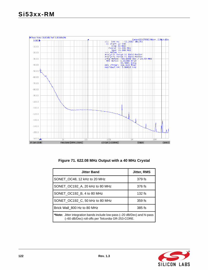
Si53xx-RM
122 Rev. 1.3
Figure 71. 622.08 MHz Output with a 40 MHz Crystal
Jitter Band Jitter, RMS
SONET_OC48, 12 kHz to 20 MHz 379 fs
SONET_OC192_A, 20 kHz to 80 MHz 376 fs
SONET_OC192_B, 4 to 80 MHz 132 fs
SONET_OC192_C, 50 kHz to 80 MHz 359 fs
Brick Wall_800 Hz to 80 MHz 385 fs
*Note: Jitter integration bands include low-pass (–20 dB/Dec) and hi-pass (–60 dB/Dec) roll-offs per Telcordia GR-253-CORE.

Si53xx-RM
Rev. 1.3 123
APPENDIX C—TYPICAL PHASE NOISE PLOTS
IntroductionThe following are some typical phase noise plots. The clock input source is a Rohde and Schwarz model SML03RF Generator. Except as noted, the phase noise analysis equipment is the Agilent E5052B. Also (except as noted),the Any-Frequency part was an Si5326 operating at 3.3 V with an ac-coupled differential PECL output and an ac-coupled differential sine wave input from the RF generator at 0 dBm. Note that, as with any PLL, the output jitterthat is below the loop bandwidth of the Any-Frequency device is caused by the jitter of the input clock, not the Any-Frequency Precision Clock. Except as noted, the loop bandwidths were 60 Hz to 100 Hz.
Figure 72. 155.52 MHz In; 622.08 MHz Out

Si53xx-RM
124 Rev. 1.3
Figure 73. 155.52 MHz In; 622.08 MHz Out; Loop BW = 7 Hz, Si5324
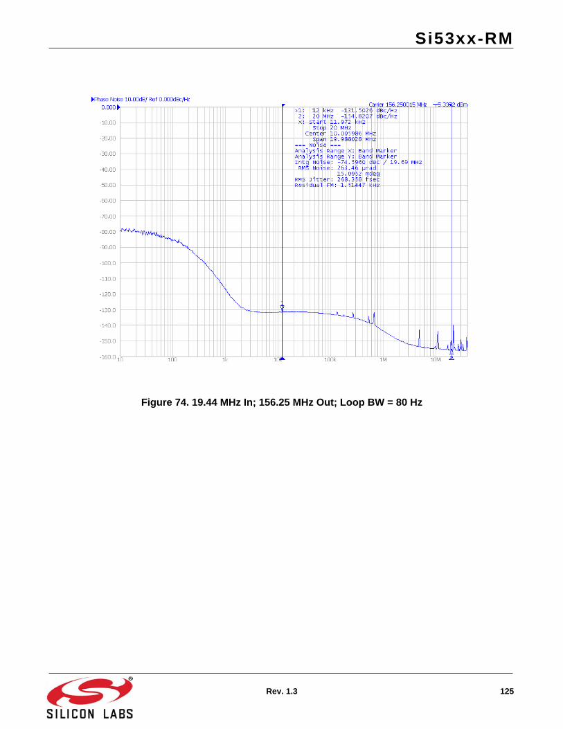
Si53xx-RM
Rev. 1.3 125
Figure 74. 19.44 MHz In; 156.25 MHz Out; Loop BW = 80 Hz

Si53xx-RM
126 Rev. 1.3
Figure 75. 19.44 MHz In; 156.25 MHz Out; Loop BW = 5 Hz, Si5324
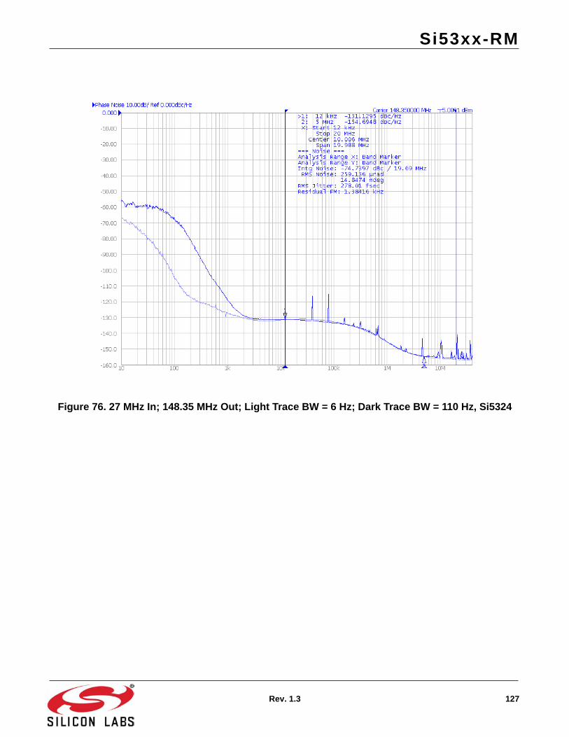
Si53xx-RM
Rev. 1.3 127
Figure 76. 27 MHz In; 148.35 MHz Out; Light Trace BW = 6 Hz; Dark Trace BW = 110 Hz, Si5324

Si53xx-RM
128 Rev. 1.3
Figure 77. 61.44 MHz In; 491.52 MHz Out; Loop BW = 7 Hz, Si5324

Si53xx-RM
Rev. 1.3 129
Figure 78. 622.08 MHz In; 672.16 MHz Out; Loop BW = 6.9 kHz

Si53xx-RM
130 Rev. 1.3
Figure 79. 622.08 MHz In; 672.16 MHz Out; Loop BW = 100 Hz

Si53xx-RM
Rev. 1.3 131
Figure 80. 156.25 MHz In; 155.52 MHz Out

Si53xx-RM
132 Rev. 1.3
Figure 81. 78.125 MHz In; 644.531 MHz Out
Table 54. Jitter Values for Figure 74
Jitter Bandwidth 644.531 MHzJitter (RMS)
Broadband, 1 kHz to 10 MHz 223 fs
OC-48, 12 kHz to 20 MHz 246 fs
OC-192, 20 kHz to 80 MHz 244 fs
OC-192, 4 MHz to 80 MHz 120 fs
OC-192, 50 kHz to 80 MHz 234 fs
Broadband, 800 Hz to 80 MHz 248 fs

Si53xx-RM
Rev. 1.3 133
Figure 82. 78.125 MHz In; 690.569 MHz Out
Table 55. Jitter Values for Figure 75
Jitter Bandwidth 690.569 MHzJitter (RMS)
Broadband, 1 kHz to 10 MHz 244 fs
OC-48, 12 kHz to 20 MHz 260 fs
OC-192, 20 kHz to 80 MHz 261 fs
OC-192, 4 MHz to 80 MHz 120 fs
OC-192, 50 kHz to 80 MHz 253 fs
Broadband, 800 Hz to 80 MHz 266 fs

Si53xx-RM
134 Rev. 1.3
Figure 83. 78.125 MHz In; 693.493 MHz Out
Table 56. Jitter Values for Figure 76
Jitter Bandwidth 693.493 MHzJitter (RMS)
Broadband, 1 kHz to 10 MHz 243 fs
OC-48, 12 kHz to 20 MHz 265 fs
OC-192, 20 kHz to 80 MHz 264 fs
OC-192, 4 MHz to 80 MHz 124 fs
OC-192, 50 kHz to 80 MHz 255 fs
Broadband, 800 Hz to 80 MHz 269 fs

Si53xx-RM
Rev. 1.3 135
Figure 84. 86.685 MHz In; 173.371 MHz and 693.493 MHz Out
Table 57. Jitter Values for Figure 77
Jitter Bandwidth 173.371 MHzJitter (RMS)
693.493 MHzJitter (RMS)
Broadband, 1 kHz to 10 MHz 262 fs 243 fs
OC-48, 12 kHz to 20 MHz 297 fs 265 fs
OC-192, 20 kHz to 80 MHz 309 fs 264 fs
OC-192, 4 MHz to 80 MHz 196 fs 124 fs
OC-192, 50 kHz to 80 MHz 301 fs 255 fs
Broadband, 800 Hz to 80 MHz 313 fs 269 fs
Red = 693.493 MHz Blue = 173.371 MHz
86.685 MHz in, 173.371 MHz and 693.493 MHz out
-1.80E+02
-1.60E+02
-1.40E+02
-1.20E+02
-1.00E+02
-8.00E+01
-6.00E+01
-4.00E+01
-2.00E+01
0.00E+00
1.00E+02 1.00E+03 1.00E+04 1.00E+05 1.00E+06 1.00E+07 1.00E+08
Offset Frequency (Hz)
Phas
e No
ise
(dBc
/Hz)

Si53xx-RM
136 Rev. 1.3
Figure 85. 86.685 MHz In; 173.371 MHz Out

Si53xx-RM
Rev. 1.3 137
Figure 86. 86.685 MHz In; 693.493 MHz Out

Si53xx-RM
138 Rev. 1.3
Figure 87. 155.52 MHz and 156.25 MHz In; 622.08 MHz Out
Table 58. Jitter Values for Figure 80
Jitter Bandwidth 155.52 MHz InputJitter (RMS)
156.25 MHz InputJitter (RMS)
Broadband, 100 Hz to 10 MHz 4432 fs 4507 fs
OC-48, 12 kHz to 20 MHz 249 fs 251 fs
OC-192, 20 kHz to 80 MHz 274 fs 271 fs
OC-192, 4 MHz to 80 MHz 166 fs 164 fs
OC-192, 50 kHz to 80 MHz 267 fs 262 fs
Broadband, 800 Hz to 80 MHz 274 fs 363 fs
Blue = 155.52 MHz Red = 156.25 MHz
155.52 MHz and 156.25MHz in, 622.08 MHz out0.00E+00
-6.00E+01
-4.00E+01
-2.00E+01
Bc/
Hz)
-1.00E+02
-8.00E+01
6.00E 01
ase
No
ise
(dB
-1.40E+02
-1.20E+02Ph
a
-1.60E+021.00E+02 1.00E+03 1.00E+04 1.00E+05 1.00E+06 1.00E+07 1.00E+08
Offset Frequency (Hz)
Blue = 155.52 MHz input Red = 156.25 MHz input

Si53xx-RM
Rev. 1.3 139
Figure 88. 10 MHz In; 1 GHz Out

Si53xx-RM
140 Rev. 1.3
Digital Video (HD-SDI)
Phase noise equipment: Agilent model JS500.
Jitter Band Jitter
Brick Wall, 10 Hz to 20 MHz 2.42 ps, RMS
Peak-to-peak 14.0 ps

Si53xx-RM
Rev. 1.3 141
APPENDIX D—ALARM STRUCTURE
Figure 89. Si5324, Si5326, and Si5328 Alarm Diagram
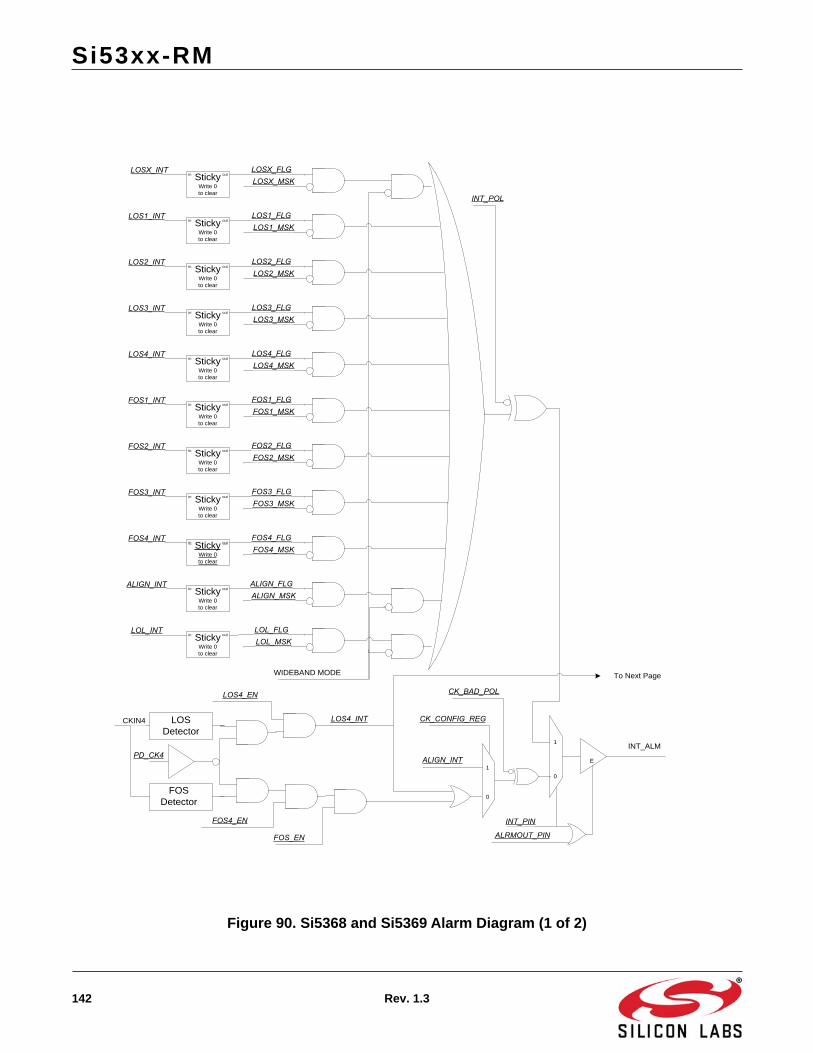
Si53xx-RM
142 Rev. 1.3
Figure 90. Si5368 and Si5369 Alarm Diagram (1 of 2)
in outStickyWrite 0to clear
in outStickyWrite 0to clear
in outStickyWrite 0to clear
in outStickyWrite 0to clear
in outStickyWrite 0to clear
in outStickyWrite 0to clear
in outStickyWrite 0to clear
in outStickyWrite 0to clear
in outStickyWrite 0to clear
in outStickyWrite 0to clear
in outStickyWrite 0to clear
WIDEBAND MODE
LOSDetector
FOSDetector
INT_ALM
E
1
01
0
CKIN4
To Next Page

Si53xx-RM
Rev. 1.3 143
Figure 91. Si5368 and Si5369 Alarm Diagram (2 of 2)

Si53xx-RM
144 Rev. 1.3
APPENDIX E—INTERNAL PULLUP, PULLDOWN BY PINTables 59–70 show which 2-Level CMOS pins have pullups or pulldowns. Note the value of the pullup/pulldownresistor is typically 75 k.
Table 59. Si5316 Pullup/Down
Pin # Si5316 Pull?
1 RST U
11 RATE0 U, D
14 DBL2_BY U, D
15 RATE1 U, D
21 CS U, D
22 BWSEL0 U, D
23 BWSEL1 U, D
24 FRQSEL0 U, D
25 FRQSEL1 U, D
26 CK1DIV U, D
27 CK2DIV U, D
30 SFOUT1 U, D
33 SFOUT0 U, D
Table 60. Si5322 Pullup/Down
Pin # Si5322 Pull?
1 RST U
2 FRQTBL U, D
9 AUTOSEL U, D
14 DBL2_BY U, D
21 CS_CA U, D
22 BWSEL0 U, D
23 BWSEL1 U, D
24 FRQSEL0 U, D
25 FRQSEL1 U, D
26 FRQSEL2 U, D
27 FRQSEL3 U, D
30 SFOUT1 U, D
33 SFOUT0 U, D

Si53xx-RM
Rev. 1.3 145
Table 61. Si5323 Pullup/Down
Pin # Si5323 Pull?
1 RST U
2 FRQTBL U, D
9 AUTOSEL U, D
11 RATE0 U, D
14 DBL2_BY U, D
15 RATE1 U, D
19 DEC D
20 INC D
21 CS_CA U, D
22 BWSEL0 U, D
23 BWSEL1 U, D
24 FRQSEL0 U, D
25 FRQSEL1 U, D
26 FRQSEL2 U, D
27 FRQSEL3 U, D
30 SFOUT1 U, D
33 SFOUT0 U, D
Table 62. Si5319, Si5324, Si5328 Pullup/Down
Pin # Si5326 Pull?
1 RST U
11 RATE0 U, D
15 RATE1 U, D
21 CS_CA U, D
22 SCL D
24 A0 D
25 A1 D
26 A2_SS D
27 SDI D
36 CMODE U, D

Si53xx-RM
146 Rev. 1.3
Table 63. Si5325 Pullup/Down
Pin # Si5325 Pull?
1 RST U
21 CS_CA U, D
22 SCL D
24 A0 D
25 A1 D
26 A2_SS D
27 SDI D
36 CMODE U, D
Table 64. Si5326 Pullup/Down
Pin # Si5326 Pull?
1 RST U
11 RATE0 U, D
15 RATE1 U, D
19 DEC D
20 INC D
21 CS_CA U, D
22 SCL D
24 A0 D
25 A1 D
26 A2_SS D
27 SDI D
36 CMODE U, D

Si53xx-RM
Rev. 1.3 147
Table 65. Si5327 Pullup/Down
Pin # Si5327 Pull?
1 RST U
11 RATE U, D
21 CKSEL U, D
22 SCL D
24 A0 D
25 A1 D
26 A2_SS D
27 SDI D
36 CMODE U, D
Table 66. Si5365 Pullup/Down
Pin # Si5365 Pull?
3 RST U
4 FRQTBL U, D
13 CS0_C3A D
22 AUTOSEL U, D
37 DBL2_BY U, D
50 DSBL5 U, D
57 CS1_C4A U, D
60 BWSEL0 U, D
61 BWSEL1 U, D
66 DIV34_0 U, D
67 DIV34_1 U, D
68 FRQSEL0 U, D
69 FRQSEL1 U, D
70 FRQSEL2 U, D
71 FRQSEL3 U, D
80 SFOUT1 U, D
85 DBL34 U
95 SFOUT0 U, D
Table 67. Si5366 Pullup/Down
Pin # Si5366 Pull?
3 RST U
4 FRQTBL U, D
13 CS0_C3A D
20 FS_SW D
21 FS_ALIGN D
22 AUTOSEL U, D
32 RATE0 U, D
37 DBL2_BY U, D
42 RATE1 U, D
50 DBL_FS U, D
51 CK_CONF D
54 DEC D
55 INC D
56 FOS_CTL U, D
57 CS1_C4A U, D
60 BWSEL0 U, D
61 BWSEL1 U, D
66 DIV34_0 U, D
67 DIV34_1 U, D
68 FRQSEL0 U, D
69 FRQSEL1 U, D
70 FRQSEL2 U, D
71 FRQSEL3 U, D
80 SFOUT1 U, D
85 DSBL34 U
95 SFOUT0 U, D

Si53xx-RM
148 Rev. 1.3
Table 68. Si5367 Pullup/Down
Pin # Si5367 Pull?
3 RST U
13 CS0_C3A D
57 CS1_C4A U, D
60 SCL D
68 A0 D
69 A1 D
70 A2_SSB D
71 SDI D
90 CMODE U, D
Table 69. Si5368 Pullup/Down
Pin # Si5368 Pull?
3 RST U
13 CS0_C3A D
21 FS_ALIGN D
32 RATE0 U, D
42 RATE1 U, D
54 DEC D
55 INC D
57 CS1_C4A U, D
60 SCL D
68 A0 D
69 A1 D
70 A2_SSB D
71 SDI D
90 CMODE U, D

Si53xx-RM
Rev. 1.3 149
Table 70. Si5369 Pullup/Down
Pin # Si5368 Pull?
3 RST U
13 CS0_C3A D
21 FS_ALIGN D
32 RATE0 U, D
42 RATE1 U, D
57 CS1_C4A U, D
60 SCL D
68 A0 D
69 A1 D
70 A2_SSB D
71 SDI D
90 CMODE U, D
Table 71. Si5374/75/76 Pullup/Down
Pin # Si5374/75/76 Pull?
D4 RSTL_A U
D6 RSTL_B U
F6 RSTL_C U
F4 RSTL_D U
D1 CS_CA_A U/D
A6 CS_CA_B U/D
F9 CS_CA_C U/D
J4 CS_CA_A U/D
G5 SCL D

Si53xx-RM
150 Rev. 1.3
APPENDIX F—TYPICAL PERFORMANCE: BYPASS MODE, PSRR,CROSSTALK, OUTPUT FORMAT JITTERThis appendix is divided into the following four sections:
Bypass Mode Performance
Power Supply Noise Rejection
Crosstalk
Output Format Jitter
Bypass: 622.08 MHz In, 622.08 MHz Out
Normal, Locked
In Digital Hold In Bypass Marconi RF Source
Jitter Bandwidth Jitter (RMS) Jitter (RMS) Jitter (RMS) Jitter (RMS)
Broadband, 1000 Hz to 10 MHz 296 fs 294 fs 2,426 fs 249 fs
OC-48, 12 kHz to 20 MHz 303 fs 304 fs 2,281 fs 236 fs
OC-192, 20 kHz to 80 MHz 321 fs 319 fs 3,079fs 352 fs
OC-192,4 MHz to 80 MHz 169 fs 165 fs 2,621 fs 305 fs
OC-192, 50 kHz to 80 MHz 304 fs 303 fs 3,078 fs 340 fs
Broadband, 800 Hz to 80 MHz 329 fs 325 fs 3,076 fs 370 fs
Dark blue — normal, locked Pink — bypassLight blue — digital hold Green — Marconi RF generator

Si53xx-RM
Rev. 1.3 151
Power Supply Noise Rejection
38.88 MHz in, 155.52 MHz out; Bandwidth = 110 Hz

Si53xx-RM
152 Rev. 1.3
Clock Input Crosstalk Results: Test Conditions
Jitter Band 155.52 MHz in, 622 MHz out,
For reference,No crosstalk
155.521 MHz in,622.084 MHz
out,No crosstalk
155.521 MHz in,622.084 MHz
out,155.52 MHz
Xtalk,99 Hz loop Bandwidth
155.521 MHz in,622.084 MHz
out,155.52 MHz
Xtalk,6.72 kHz loop
Bandwidth
155.521 MHz in,622.084 MHz
out,155.52 MHz
Xtalk,In digital hold
OC-48, 12 kHz to 20 MHz
262 fs 262 fs 269 fs 422 fs 255 fs
OC-192, 20 kHz to 80 MHz
287 fs 290 fs 296 fs 366 fs 280 fs
Broadband, 800 Hz to 80 MHz
285 fs 289 fs 298 fs 1,010 fs 277 fs
Measurement conditions:1. Using Si5365/66-EVB.2. Clock input on CKIN1, a 0dBm sine wave from Rohde and Schwarz RF Generator, model SML033. Crosstalk interfering signal applied to CKIN3, a PECL output at 155.52 MHz 4. All differential, AC coupled signals

Si53xx-RM
Rev. 1.3 153
Clock Input Crosstalk: Phase Noise Plots
Dark blue — No crosstalkLight blue — With crosstalk, low bandwidthYellow — With crosstalk, high bandwidthRed — With crosstalk, in digital hold

Si53xx-RM
154 Rev. 1.3
Clock Input Crosstalk: Detail View
Dark blue — No crosstalkLight blue — With crosstalk, low bandwidthYellow — With crosstalk, high bandwidthRed — With crosstalk, in digital hold
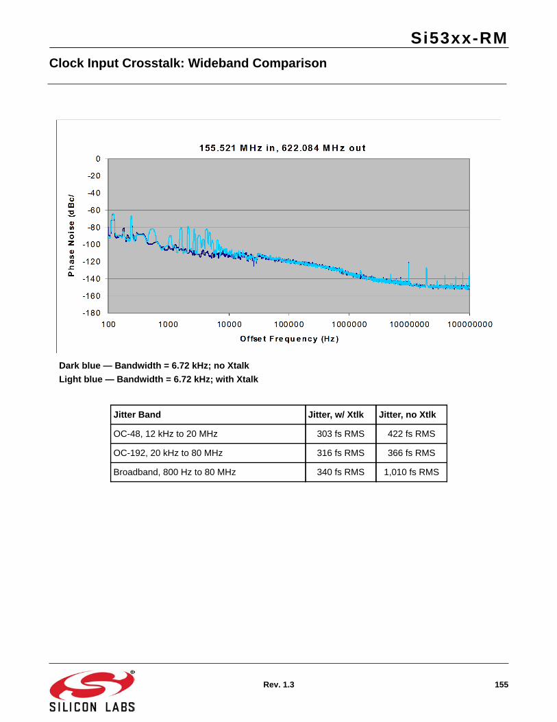
Si53xx-RM
Rev. 1.3 155
Clock Input Crosstalk: Wideband Comparison
Dark blue — Bandwidth = 6.72 kHz; no XtalkLight blue — Bandwidth = 6.72 kHz; with Xtalk
Jitter Band Jitter, w/ Xtlk Jitter, no Xtlk
OC-48, 12 kHz to 20 MHz 303 fs RMS 422 fs RMS
OC-192, 20 kHz to 80 MHz 316 fs RMS 366 fs RMS
Broadband, 800 Hz to 80 MHz 340 fs RMS 1,010 fs RMS

Si53xx-RM
156 Rev. 1.3
Clock Input Crosstalk: Output of Rohde and Schwartz RF

Si53xx-RM
Rev. 1.3 157
Jitter vs. Output Format: 19.44 MHz In, 622.08 MHz Out
Spectrum Analyzer: Agilent Model E444OA
Table 72. Output Format vs. Jitter
Bandwidth LVPECL Jitter (RMS)
LVDS Jitter (RMS)
CML Jitter (RMS) Low Swing LVDS Jitter (RMS)
Broadband, 1 kHz to 10 MHz 282 fs 269 fs 257 fs 261 fs
OC-48, 12 kHz to 20 MHz 297 fs 289 fs 290 fs 291 fs
OC-192, 20 kHz to 80 MHz 315 fs 327 fs 358 fs 362 fs
OC-192, 4 MHz to 80 MHz 180 fs 222 fs 277 fs 281 fs
OC-192, 50 kHz to 80 MHz 299 fs 313 fs 348 fs 351 fs
Broadband, 800 Hz to 80 MHz 325 fs 332 fs 357 fs 360 fs

Si53xx-RM
158 Rev. 1.3
APPENDIX G—NEAR INTEGER RATIOSTo provide more details and to provide boundaries with respect to the “Reference vs. Output Frequency” issuedescribed in Appendix B on page 116, the following study was performed and is presented below.
Test Conditions XA/XB External Reference held constant at 38.88 MHz
Input frequency centered at 155.52 MHz, then scanned.Scan Ranges and Resolutions:± 50 ppm with 2 ppm steps± 200 ppm with 10 ppm steps± 2000 ppm with 50 ppm steps
Output frequency always exactly four times the input frequencyCentered at 622.08 MHz
Jitter values are RMS, integrated from 800 Hz to 80 MHz
Figure 92. ±50 ppm, 2 ppm Steps
Input Frequency Variation = ±50 ppm
38.88 MHz External XA-XB Reference
0
200
400
600
800
1000
1200
155.51 155.515 155.52 155.525 155.53
Input Frequency (MHz)
RM
S ji
tter,
fs

Si53xx-RM
Rev. 1.3 159
Figure 93. ±200 ppm, 10 ppm Steps
Figure 94. ±2000 ppm, 50 ppm Steps
Input Frequency Variation = ±200 ppm
38.88 MHz External XA-XB Reference
0
200
400
600
800
1000
1200
155.49 155.5 155.51 155.52 155.53 155.54 155.55
Input Frequency (MHz)
RM
S ji
tter,
fs
Input Frequency Variation = ±2000 ppm
38.88 MHz External XA-XB Reference
0
200
400
600
800
1000
1200
155.2 155.3 155.3 155.4 155.4 155.5 155.5 155.6 155.6 155.7 155.7 155.8 155.8 155.9 155.9
Input Frequency (MHz)
RM
S ji
tter,
fs

Si53xx-RM
160 Rev. 1.3
APPENDIX H—JITTER ATTENUATION AND LOOP BWThe following illustrates the effects of different loop BW values on the jitter attenuation of the Any-Frequencydevices. The jitter consists of sine wave modulation at varying frequencies. The RMS jitter values of the modulatedsine wave input is compared to the output jitter of an Si5326 and an Si5324. For reference, the top entry in thetable lists the jitter without any modulation. For each entry in the table, the corresponding phase noise plots arepresented.
Table 73. Jitter Values
Fmod Fdev Jitter Start RF Gen Si5326 Si5324
0 0 500 Hz 1.18 ps 283 fs 281 fs
50 Hz 50 Hz 10 Hz 181 ps 169 ps 10.6 ps
100 Hz 100 Hz 50 Hz 177 ps 136 ps 2.04 ps
500 Hz 500 Hz 100 Hz 175 ps 18.6 ps 295 fs
1 kHz 1 kHz 500 Hz 184 ps 4.28 ps 292 fs
5 kHz 5 kHz 500 Hz 138 ps 297 fs 302 fs
10 kHz 10 kHz 500 Hz 139 ps 302 fs 304 fs
Notes:1. All phase noise plots are with 622.08 MHz input and 622.08 MHz output.
Si5326 bandwidth = 120 Hz; Si5324 bandwidth = 7 Hz.2. FM modulation at F = Fmod with modulation amplitude = Fdev.3. Jitter start is the start of the brick wall integration band. All integration bands end at 50 MHz.4. Phase noise measured by Agilent model E5052B.5. RF Generator was Rohde and Schwarz model SML03.

Si53xx-RM
Rev. 1.3 161
Figure 95. RF Generator, Si5326, Si5324; No Jitter (For Reference)
Figure 96. RF Generator, Si5326, Si5324 (50 Hz Jitter)
Blue = RF Generator Green = Si5326 Red = Si5324
622.08 MHz in, 622.08 MHz out
-1.80E+02
-1.60E+02
-1.40E+02
-1.20E+02
-1.00E+02
-8.00E+01
-6.00E+01
-4.00E+01
-2.00E+01
0.00E+00
1.00E+01 1.00E+02 1.00E+03 1.00E+04 1.00E+05 1.00E+06 1.00E+07 1.00E+08
Offset Frequency (Hz)
Phas
e No
ise
(dBc
/Hz)
Blue = RF Generator Green = Si5326 Red = Si5324
622.08 MHz in, 622.08 MHz out
-1.80E+02
-1.60E+02
-1.40E+02
-1.20E+02
-1.00E+02
-8.00E+01
-6.00E+01
-4.00E+01
-2.00E+01
0.00E+00
1.00E+01 1.00E+02 1.00E+03 1.00E+04 1.00E+05 1.00E+06 1.00E+07 1.00E+08
Offset Frequency (Hz)
Phas
e No
ise
(dBc
/Hz)

Si53xx-RM
162 Rev. 1.3
Figure 97. RF Generator, Si5326, Si5324 (100 Hz Jitter)
Figure 98. RF Generator, Si5326, Si5324 (500 Hz Jitter)
Blue = RF Generator Green = Si5326 Red = Si5324
622.08 MHz in, 622.08 MHz out
-1.80E+02
-1.60E+02
-1.40E+02
-1.20E+02
-1.00E+02
-8.00E+01
-6.00E+01
-4.00E+01
-2.00E+01
0.00E+00
1.00E+01 1.00E+02 1.00E+03 1.00E+04 1.00E+05 1.00E+06 1.00E+07 1.00E+08
Offset Frequency (Hz)
Phas
e No
ise
(dBc
/Hz)
Blue = RF Generator Green = Si5326 Red = Si5324
-1.80E+02
-1.60E+02
-1.40E+02
-1.20E+02
-1.00E+02
-8.00E+01
-6.00E+01
-4.00E+01
-2.00E+01
0.00E+00
1.00E+02 1.00E+03 1.00E+04 1.00E+05 1.00E+06 1.00E+07 1.00E+08
Pha
se N
oise
(dB
c/H
z)
Offset Frequency (Hz)
622.08 MHz in, 622.08 MHz out

Si53xx-RM
Rev. 1.3 163
Figure 99. RF Generator, Si5326, Si5324 (1 kHz Jitter)
Figure 100. RF Generator, Si5326, Si5324 (5 kHz Jitter)
Blue = RF Generator Green = Si5326 Red = Si5324
622.08 MHz in, 622.08 MHz out
-1.80E+02
-1.60E+02
-1.40E+02
-1.20E+02
-1.00E+02
-8.00E+01
-6.00E+01
-4.00E+01
-2.00E+01
0.00E+00
1.00E+02 1.00E+03 1.00E+04 1.00E+05 1.00E+06 1.00E+07 1.00E+08
Offset Frequency (Hz)
Pha
se N
oise
(dB
c/H
z)
Blue = RF Generator Green = Si5326 Red = Si5324
622.08 MHz in, 622.08 MHz out
-1.80E+02
-1.60E+02
-1.40E+02
-1.20E+02
-1.00E+02
-8.00E+01
-6.00E+01
-4.00E+01
-2.00E+01
0.00E+00
1.00E+02 1.00E+03 1.00E+04 1.00E+05 1.00E+06 1.00E+07 1.00E+08
Offset Frequency (Hz)
Phas
e No
ise
(dBc
/Hz)

Si53xx-RM
164 Rev. 1.3
Figure 101. RF Generator, Si5326, Si5324 (10 kHz Jitter)
Blue = RF Generator Green = Si5326 Red = Si5324
622.08 MHz in, 622.08 MHz out
-1.80E+02
-1.60E+02
-1.40E+02
-1.20E+02
-1.00E+02
-8.00E+01
-6.00E+01
-4.00E+01
-2.00E+01
0.00E+00
1.00E+02 1.00E+03 1.00E+04 1.00E+05 1.00E+06 1.00E+07 1.00E+08
Offset Frequency (Hz)
Phas
e No
ise
(dBc
/Hz)

Si53xx-RM
Rev. 1.3 165
APPENDIX I—RESPONSE TO A FREQUENCY STEP FUNCTIONWhen an input clock is switched between two clocks that differ in frequency, the PLL will adjust to the new clockfrequency at a rate that depends on the PLL's loop bandwidth value. This process is the same if a single clock inputabruptly changes frequency. If a PLL has a lower loop bandwidth, its response to such a sudden change in inputfrequency will be slower than a PLL with a higher loop bandwidth value. Figure 102 shows a measurement of theoutput of an Si5326 during a clock switch from a 100 MHz clock input to a 100 MHz + 100 ppm clock input(100.01 MHz) with a loop BW of 120 Hz. The horizontal scale is time, in seconds. The vertical scale is the Si5326output frequency in Hz.
Figure 102. Si5326 Frequency Step Function Response

Si53xx-RM
166 Rev. 1.3
APPENDIX J—Si5374, Si5375, Si5376 PCB LAYOUT RECOMMENDATIONSThe following is a set of recommendations and guidelines for printed circuit board layout with the Si5374, Si5375,and Si5376 devices. Because the four DSPLLs are in close physical and electrical proximity to one another, PCBlayout is critical to achieving the highest levels of jitter performance. The following images were taken from theSi537x-EVB (evaluation board) layout. For more details about this board, refer to the Si537x-EVB Evaluation BoardUser's Guide.
Figure 103. Vdd Plane Use a solid and undisturbed ground plane for the Si537x and all of the clock input and output return paths.
For applications that wish to logically connect the four RSTL_x signals, do not tie them together underneath theBGA package. Instead connect them outside of the BGA footprint.
Where possible, place the CKOUT and CKIN signals on separate PCB layers with a ground layer betweenthem. The use of ground guard traces between all clock inputs and outputs is recommended.

Si53xx-RM
Rev. 1.3 167
Figure 104. Ground Plane and ResetRSTL_x PinsIt is highly recommended that the four RSTL_x pins (RSTL_A, RSTL_B, RSTL_C and RSTL_D) be logicallyconnected to one another so that the four DSPLLs are always either all in reset or are all out of reset. While inreset, the DSPLLs VCO will continue to run, and, because the VCOs will not be locked to any signal, they will driftand can be any frequency value within the VCO range. If a drifting VCO happens to have a frequency value that isclose to an operational DSPLLs VCO, there could be crosstalk between the two VCOs. To avoid this issue, Si537xDSPLLsim initializes the four DSPLLs with default Free Run frequency plans so that the VCO values are apart fromone another. If the four RSTL_x pins are directly connected to one another, the connections should not occurdirectly underneath the BGA package. Instead, the connections should occur outside of the package footprint.

Si53xx-RM
168 Rev. 1.3
The following is a set of recommendations and guidelines for printed circuit board layout with the Si5374, Si5375,and Si5376 devices. Because the four DSPLLs are in close physical and electrical proximity to one another, PCBlayout is critical to achieving the highest levels of jitter performance. The following images were taken from theSi537x-EVB (evaluation board) layout. For more details about this board, please refer to the Si537x-EVBEvaluation Board User's Guide.
Figure 105. Output Clock Routing

Si53xx-RM
Rev. 1.3 169
Figure 106. OSC_P, OSC_N Routing

Si53xx-RM
170 Rev. 1.3
APPENDIX K—Si5374, Si5375, AND Si5376 CROSSTALKWhile the four DSPLLs of the Si5374, Si5375, and Si5376 are in close physical and electrical proximity to oneanother, crosstalk interference between the DSPLLs is minimal. The following measurements show typicalperformance levels that can be expected for the Si5374, Si5375, and Si5376 when all four of their DSPLLs areoperating at frequencies that are close in value to one another, but not exactly the same.
Si5374, Si5375, and Si5376 Crosstalk Test BedAll four DSPLLs share the same frequency plan:
38.88 MHz input.
38.88 MHz x 4080 / 227 = 698.81 MHz output (rounded).
There are four slightly different input frequencies:
DSPLL A: 38.88 MHz + 0 ppm => 38.88000000 MHz
DSPLL B: 38.88 MHz + 1 ppm => 38.88003888 MHz
DSPLL C: 38.88 MHz + 10 ppm => 38.88038880 MHz
DSPLL D: 38.88 MHz + 20 ppm => 38.88077760 MHz
OSC_P, OSC_N Reference:
Si530 at 121.109 MHz
Test equipment:
Agilent E5052B
Table 74. Si5374/75/76 Crosstalk Jitter Values
DSPLL Jitter, fsec RMS
A 334
B 327
C 358
D 331

Si53xx-RM
Rev. 1.3 171
Figure 107. Si5374, Si5375, and Si5376 DSPLL A
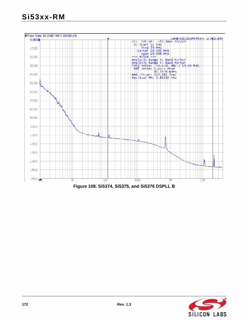
Si53xx-RM
172 Rev. 1.3
Figure 108. Si5374, Si5375, and Si5376 DSPLL B

Si53xx-RM
Rev. 1.3 173
Figure 109. Si5374, Si5375, and Si5376 DSPLL C
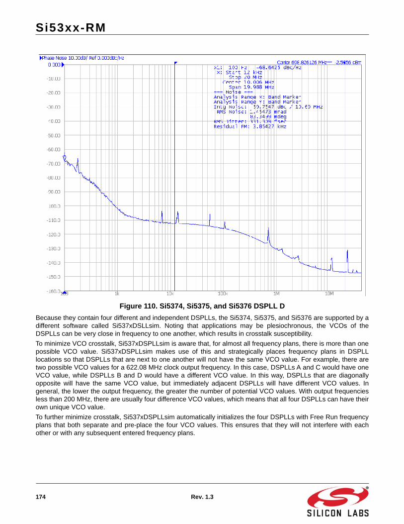
Si53xx-RM
174 Rev. 1.3
Figure 110. Si5374, Si5375, and Si5376 DSPLL DBecause they contain four different and independent DSPLLs, the Si5374, Si5375, and Si5376 are supported by adifferent software called Si537xDSLLsim. Noting that applications may be plesiochronous, the VCOs of theDSPLLs can be very close in frequency to one another, which results in crosstalk susceptibility.
To minimize VCO crosstalk, Si537xDSPLLsim is aware that, for almost all frequency plans, there is more than onepossible VCO value. Si537xDSPLLsim makes use of this and strategically places frequency plans in DSPLLlocations so that DSPLLs that are next to one another will not have the same VCO value. For example, there aretwo possible VCO values for a 622.08 MHz clock output frequency. In this case, DSPLLs A and C would have oneVCO value, while DSPLLs B and D would have a different VCO value. In this way, DSPLLs that are diagonallyopposite will have the same VCO value, but immediately adjacent DSPLLs will have different VCO values. Ingeneral, the lower the output frequency, the greater the number of potential VCO values. With output frequenciesless than 200 MHz, there are usually four difference VCO values, which means that all four DSPLLs can have theirown unique VCO value.
To further minimize crosstalk, Si537xDSPLLsim automatically initializes the four DSPLLs with Free Run frequencyplans that both separate and pre-place the four VCO values. This ensures that they will not interfere with eachother or with any subsequent entered frequency plans.

Si53xx-RM
Rev. 1.3 175
Si5374/75/76 Register Map Partition ExampleIn a typical line card application, an Si5374/75/76 will supply four clocks to four different channels that might needto support any combination of services. For example, say that each of the four DSPLLs (A, B, C or D) can beprogrammed for either a SONET, OTN/OTU or Ethernet frequency plan in any combination. In this example, callthe SONET plan P1, the OTN/OTU plan P2 and the Ethernet plan P3. Further, assume that there is a need fordynamic allocation of services at run time. To avoid crosstalk between DSPLLs programmed with similar serviceswhich may have operating frequencies that are close but not exactly the same, the following procedure issuggested:
Run Si537xDSPLLsim three times, once each for OTN/OTU, Ethernet and SONET. This will result in three registermaps that are each comprised of four sub-maps A, B, C and D, as shown below:
Figure 111. Example Frequency Plan SourcesTo accommodate a combination of the three different services at run time, the individual sub-maps from the threedifferent frequency plans can be placed into the four DSPLLs. However, it is recommended that DSPLL_A only beloaded with a sub-map that was created for DSPLL_A and not with a sub-map created for any of the other threeDSPLLs, as shown below:

Si53xx-RM
176 Rev. 1.3
Figure 112. Run Time Frequency Plan Examples
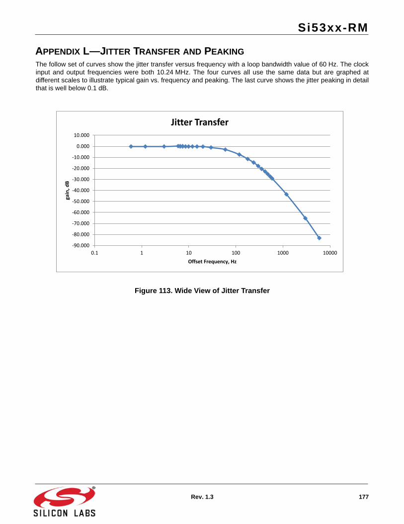
Si53xx-RM
Rev. 1.3 177
APPENDIX L—JITTER TRANSFER AND PEAKINGThe follow set of curves show the jitter transfer versus frequency with a loop bandwidth value of 60 Hz. The clockinput and output frequencies were both 10.24 MHz. The four curves all use the same data but are graphed atdifferent scales to illustrate typical gain vs. frequency and peaking. The last curve shows the jitter peaking in detailthat is well below 0.1 dB.
Figure 113. Wide View of Jitter Transfer
-90.000
-80.000
-70.000
-60.000
-50.000
-40.000
-30.000
-20.000
-10.000
0.000
10.000
0.1 1 10 100 1000 10000
gain
, dB
Offset Frequency, Hz
Jitter Transfer

Si53xx-RM
178 Rev. 1.3
Figure 114. Zoomed View of Jitter Transfer
Figure 115. Zoomed Again View of Jitter Transfer (Showing Peaking)
-10.000
-8.000
-6.000
-4.000
-2.000
0.000
2.000
0.1 1 10 100 1000
gain
, dB
Offset Frequency, Hz
Jitter Transfer
-2.000
-1.500
-1.000
-0.500
0.000
0.500
0.1 1 10 100
gain
, dB
Offset Frequency, Hz
Jitter Transfer

Si53xx-RM
Rev. 1.3 179
Figure 116. Maximum Zoomed View of Jitter Peaking
-0.200
-0.150
-0.100
-0.050
0.000
0.050
0.100
1 10
gain
, dB
Offset Frequency, Hz
Jitter Transfer

Si53xx-RM
180 Rev. 1.3
DOCUMENT CHANGE LIST
Revision 0.3 to Revision 0.4 Updated AC Specifications in Table 8, “AC Characteristics—All Devices”
Added Si5365, Si5366, Si5367, and Si5368 operation at 3.3 V
Updated Section “6.8. Frame Synchronization Realignment (Si5368 and CK_CONFIG_REG = 1)”
Added input clock control diagrams in Section “6.4. Input Clock Control”
Added new crystals into Table 50, “Approved 114.285 MHz Crystals,” on page 108.
Updated "Appendix D—Alarm Structure" on page 141
Added "Appendix F—Typical Performance: Bypass Mode, PSRR, Crosstalk, Output Format Jitter" on page 150
Revision 0.4 to Revision 0.41 Added Si5324.
Revision 0.41 to Revision 0.42 Moved Si5326 specifications to the Si5326 data sheet.
Corrected Figure 21, “Jitter Tolerance Mask/Template.”
Simplified Section “4. Device Specifications”
Updated Figure 41, “CMOS Termination (1.8, 2.5, 3.3 V).”
Revision 0.42 to Revision 0.5 Added Si5327, Si5369, Si5374, and Si5375.
Removed Si5319 and Si5323 from the spec tables.
Updated the typical phase noise plots.
Added new appendixes G, H, I, and J.
Updated spec table values.
Added examples and diagrams throughout.
Revision 0.5 to Revision 0.51 Updated Table 50 in Appendix A.
Updated Figure 41 on page 95.
Corrected Figure 90 Alarm Diagram on page 142.

Si53xx-RM
Rev. 1.3 181
Revision 0.51 to Revision 0.52 Added “Wideband devices not recommended for new designs” language.
Added note on SCL pull-up to Table 5 on page 36.
Added a specific time period to "5.9.1. Loss-of-Signal Alarms (Si5316, Si5322, Si5323, Si5365, Si5366)" on page 60.
Changed lock time values in "6.2. PLL Self-Calibration" on page 66.
Updated Appendix B figures.
Updated Appendix J.
Added Appendix K.
Revision 0.52 to Revision 1.0 Added the Si5376
Removed Section 4 specification tables.
Updated Appendix A on page 108.
Expanded Appendix B on page 116.
Added new Appendix I on page 165.
Fixed various typos and other minor corrections.
Revision 1.0 to Revision 1.1 Added SPI timing diagram to "6.14. Serial Microprocessor Interface (SPI)" on page 91.
Reinstated the ML external clock reference band in “ Appendix A—Narrowband References”, Table 50.
Added warning about MEMS reference oscillators to “ Appendix A—Narrowband References”.
Expanded Figure 45 title.
Revision 1.1 to Revision 1.2 Added Si5328.
Updated Table 50 on page 108 to include Connor Winfield CS-023E crystal.
Revision 1.2 to Revision 1.3 Removed Table 50 on page 108
Removed approved 40 MHz crystals on page 109 (for both changes, see "Si531x/2x/6x Jitter Attenuating Clock Recommended Crystals List”.
Added general crystal applications information, formerly in obsolete AN591, to Appendix A - Narrowband References.
http://www.silabs.com
Silicon Laboratories Inc.400 West Cesar ChavezAustin, TX 78701USA
ClockBuilder ProOne-click access to Timing tools, documentation, software, source code libraries & more. Available for Windows and iOS (CBGo only).
www.silabs.com/CBPro
Timing Portfoliowww.silabs.com/timing
SW/HWwww.silabs.com/CBPro
Qualitywww.silabs.com/quality
Support and Communitycommunity.silabs.com
DisclaimerSilicon Labs intends to provide customers with the latest, accurate, and in-depth documentation of all peripherals and modules available for system and software implementers using or intending to use the Silicon Labs products. Characterization data, available modules and peripherals, memory sizes and memory addresses refer to each specific device, and "Typical" parameters provided can and do vary in different applications. Application examples described herein are for illustrative purposes only. Silicon Labs reserves the right to make changes without further notice and limitation to product information, specifications, and descriptions herein, and does not give warranties as to the accuracy or completeness of the included information. Silicon Labs shall have no liability for the consequences of use of the information supplied herein. This document does not imply or express copyright licenses granted hereunder to design or fabricate any integrated circuits. The products are not designed or authorized to be used within any Life Support System without the specific written consent of Silicon Labs. A "Life Support System" is any product or system intended to support or sustain life and/or health, which, if it fails, can be reasonably expected to result in significant personal injury or death. Silicon Labs products are not designed or authorized for military applications. Silicon Labs products shall under no circumstances be used in weapons of mass destruction including (but not limited to) nuclear, biological or chemical weapons, or missiles capable of delivering such weapons.
Trademark InformationSilicon Laboratories Inc.® , Silicon Laboratories®, Silicon Labs®, SiLabs® and the Silicon Labs logo®, Bluegiga®, Bluegiga Logo®, Clockbuilder®, CMEMS®, DSPLL®, EFM®, EFM32®, EFR, Ember®, Energy Micro, Energy Micro logo and combinations thereof, "the world’s most energy friendly microcontrollers", Ember®, EZLink®, EZRadio®, EZRadioPRO®, Gecko®, ISOmodem®, Precision32®, ProSLIC®, Simplicity Studio®, SiPHY®, Telegesis, the Telegesis Logo®, USBXpress® and others are trademarks or registered trademarks of Silicon Labs. ARM, CORTEX, Cortex-M3 and THUMB are trademarks or registered trademarks of ARM Holdings. Keil is a registered trademark of ARM Limited. All other products or brand names mentioned herein are trademarks of their respective holders.