annual performance reportireap.umd.edu/~vlg/muri2001/muri '01 annual report 04.doc · web...
TRANSCRIPT
Annual Performance Report
AFOSR Grant Number F496200110374
Descriptive Title: “Effects of High Power Microwaves and Chaos in 21st Century Analog and Digital Electronics”
Grantee Institution: Institute for Research in Electronics and Applied Physics University of Maryland. College Park 20743-3511
Principal Investigator: Victor L. Granatstein
Co-Principal Investigators: Steven Anlage
Thomas M. Antonsen, Jr.
Yuval Carmel
Neil Goldsman
Agis Iliadis
Bruce Jacob
John Melngalis
Edward Ott
Omar Ramahi
John Rodgers
Subcontract to Boise State University: Principal Investigator, R. Jacob Baker; Co-Principal Investigator, William B. Knowlton
Reporting Period: September 1, 2003 to August 31, 2004
1

TABLE OF CONTENTS Page
I. INTRODUCTION / OBJECTIVES 3
II. STATUS OF EFFORT 4
III. RESEARCH ACCOMPLISHMENTS 6 III.1 Chaos Studies III.1.a Statistical Models for Impedance and Scattering Matrices of Open Cavities 6 III.1.b Field Impedance Statistics in Complex Enclosures 9
III.2 Microwave Effects on Electronics 11 III.2.a Simulation of Microwave Effects on Electronics 11 III.2.b Characteristics of Radio Frequency Upset in CMOS Logic with Electrostatic Discharge Protection 13 III.2.c Experimental Studies of Pulsed RF Interference on IC 42 MOSFETs, Inverters and Differential Amplifiers III.3 Fabrication and Testing of On-Chip Microwave Detectors 48 III.4 Studies of Enclosures and Shielding 50
IV. PERSONNEL SUPPORTED 53 IV.1 Academic Faculty IV.2 Research Faculty IV.3 Graduate Students
V. PUBLICATIONS AND PATENTS 54 V.1 Refereed Journal Papers During the Reporting Period V.2 Papers Submitted to Refereed Journals V.3 Papers Published in Conference Proceedings V.4 Patents
VI. INTERACTIONS / TRANSITIONS 58 VI.1 Presentations at Meetings and Conferences VI.2 Interaction with DOD Laboratories, Agencies & Contractors
VII. HONORS / AWARDS 60
APPENDIX: Performance Report of Boise State University 61
2

I. INTRODUCTION / OBJECTIVES This is the fourth report on the MURI 2001 program, “Effects of high-power microwaves and chaos in analog and digital circuits”, being carried out at the University of Maryland, College Park (UMCP) with subcontract to Boise State University. The program was initiated in May 2001. The present report covers the period September 1, 2003 to August 31, 2004. The objective is to study at a fundamental level the effects of high power microwave pulses and chaos in electronic devices, circuits and systems that might lead to upset or damage. The program at UMCP has the four interrelated parts as follows:
1. Chaos studies, especially wave chaos which provides a statistical description of microwave field in complex topologies such as circuits in boxes;
2. Analysis, simulation and testing of microwave effects on devices, circuits and systems. The testing is primarily in the frequency range 300 MHz to 10 GHz while pulse duration and power level are varied;
3. Custom-design and fabrication of integrated circuits with on-chip microwave diagnostics;
4. Studies of enclosures and shielding.
Progress on each of these topics at UMCP will be reported in the body of this report.A separate report of progress at Boise State University is appended.
3

III. STATUS OF EFFORT
Our studies in the area of wave chaos have yielded a stochastic formalism for
describing the statistical properties of 3-dimensional microwave cavities which can
support multiple modes and have a complex geometry including ports and wall loses.
Salient predictions of this formalism have now been confirmed experimentally. This
work is enabling one to predict the probability distribution function of electric field on
electronic components inside a partially shielded enclosure from a knowledge of
microwave power entering a “port” (such as a cooling vent) and minimal information
about the properties of the enclosure such as its Q.
Another fruitful aspect of our recent work has emphasized the development of
simulation tools to model the effects radio frequency (RF) radiation coupling on
semiconductor devices, logic-gates and interconnects in integrated circuits. The
semiconductor device and logic-gate simulators are based on kinetic theory using
differential equations that describe the flow of electrons and holes inside nanoscale
MOSFETs. In contrast with the ubiquitous circuit simulator SPICE, which is based on
lumped analysis and uses hundreds of fitting parameters, our simulators are physics
based, and they solve distributed systems of partial differential equations. As a result, our
work allows one to probe into the device, and see precisely where the upset occurs. In
addition, since our simulator is based on physics, and not fitting parameters, it can be
used as a virtual device, from which new SPICE models can be developed, and circuits
can be designed before any costly fabrication is actually performed. In addition to
developing device simulation software, we also have made considerable progress in
developing our tool to model the interaction of RF and computer chips. This tool solves
Maxwell’s equations for the passive structures on chips. For example, bus lines, which
are designed for carrying square pulses become on-chip transmission lines. The
transmission lines are metal-insulator-semiconductor-metal structures. The coupling of
RF to these depends on their precise geometry and semiconductor doping. Our simulator
is designed to analyze these structures in detail. We have used it to identify slow-wave,
quasi-dielectric and skin effect modes in on-chip transmission lines, and the behavior of
on-chip passive elements including inductors. We plan to continue this work, focus on
4

various integrated circuit upset phenomena, including the transient modeling of
nanometer MOSFET thin gate-oxide breakdown.
In experimental studies of the interaction of RF with integrated circuits, we have
found that due to their nonlinear current-voltage characteristics, the electrostatic
discharge protection devices included in most integrated circuits may unintentionally
rectify the RF signals. The envelope of the RF carrier is thereby down-converted into a
voltage that, with sufficient amplitude, could drive a logic device into upset.
Furthermore, the junction capacitances associated with the protection devices work in
concert with parasitic inductances to form resonant circuits. When these parasitic
networks are excited near resonance, the internal oscillating currents can be much higher
than the RF driving current. Thus, the envelope voltages generated by the diodes and,
consequently, the susceptibility of the device to upset, are increased. We have conducted
a theoretical, numerical and experimental investigation of the RF characteristics of
electrostatic protection diodes and the response of logic circuits to these rectified
voltages. The transfer characteristics of these effects were investigated when the device
inputs were excited by pulse-modulated carriers whose frequency was near the parasitic
resonance of the device. The results show where in the regime of excitation parameters
the radio-frequency pulses cause state errors or unstable operating conditions. Some
devices exhibit sufficiently high resonant gains to be upset by carriers with amplitudes as
low as a few hundred millivolts. The analysis presented here forms a basis for a general
approach to predicting RF effects in circuits. Good agreement between the results from
theoretical and numerical calculations and the experiments is demonstrated.
In the area of Envclosures and Shielding, the most recent accomplishments
include the following:
1. Using high permittivity material to achieve miniaturization of Electromagnetic Band Gap Structures
2. Using mixed topology Electromagnetic Band Gap structures to achieve multi-band mitigation
3. Using Electromagnetic Band Gap structures to mitigate coupling between apertures and cavities
4. Experimental validation of the aperture coating techniques to reduce resonance-enhanced radiation.
5

III. RESEARCH ACCOMPLISHMENTS
III.1 Chaos Studies( Professor Thomas M. Antonsen Jr., Professor Edward Ott, Professor Steven Anlage. Students: James Hart, Sameer Hemmady, X. Henry Zheng )
II.1.a Statistical Models for Impedance and Scattering Matrices of Open Cavities
INTRODUCTIONThe problem of the coupling of electromagnetic radiation in and out of structures is a general one that finds applications in a variety of scientific and engineering contexts. Examples include the susceptibility of circuits to electromagnetic interference, the confinement of radiation to enclosures, as well as the coupling of radiation to accelerating structures. Because of the wave nature of radiation, the coupling properties of a structure depend in detail on the size and shape of the structure, as well as the frequency of the radiation. In considerations of irregularly shaped electromagnetic enclosures for which the wavelength is fairly small compared with the size of the enclosure, it is typical that the electromagnetic field pattern within the enclosure, as well as the response to external inputs, can be very sensitive to small changes in frequency and to small changes in the configuration. Thus, knowledge of the response of one configuration of the enclosure may not be useful in predicting that of a nearly identical enclosure. This motivates a statistical approach to the electromagnetic problem [1].
We have developed a statistical approach [2], which we call the random coupling model, to describe the properties of a high-frequency microwave cavity with several ports and losses. We express the scattering matrix for this system using the cavity impedance matrix. The impedance matrix is derived in terms of the eigenfunctions and eigenfrequencies of the closed cavity. Explicit calculation of the eigenfunctions and eigenfrequencies is not required however. Rather,
6
Port 1
Port 2
Other ports
Losses
Port 1
Free-space radiationResistance RR()ZR() = RR()+jXR ()
RR1()
RR2()
Fig. 1 Schematic illustrating application of the random coupling model
Fig.2 Histograms of normalized cavity reactance for a) 6.75-7.25 GHz and b) 7.75 to 8.25 GHz

in view of the extreme sensitivity of these to the specific geometry they are replaced by functions drawn from a statistical ensemble. We find that the impedance matrix can then be expressed in terms of random variables with well-defined statistics and relatively simple, physical quantities characterizing the cavity.The method of application of our model is illustrated in Fig. 1. One first isolates the ports of interest, in this case port 1 and port 2, and computes (or measures) the free space radiation impedance for each port. The process of isolation consists of determining what is in the near field region of the port and including it in the calculation of the radiation impedance. The concept of a port can be generalized to apply to terminals on circuits within the enclosure. Each port is then characterized by the free space radiation resistance RRi(). The additional important physical quantities needed in our model are the volume of the cavity and the cavity quality factor. The impedance matrix is then modeled by the formula,
,
where, n2 is the mean spectral density of the cavity, Q is the average quality factor, win are a set
of independent, zero mean, unit variance Gaussian random numbers, and n2 is a random
spectrum determined by generating random spacings between eigenfrequencies consistent with the average spectral density. We describe in the next sections some of the predictions of this model.
CAVITY IMPEDANCE DISTRIBUTIONSWe have parameterized the probability distribution function for the real and imaginary parts of the cavity impedance. For a lossless, single port cavity the impedance is imaginary with a mean and fluctuating part. The mean part is equal to the radiation reactance for the port under the conditions of radiation into free space. The fluctuating part of the reactance is Lorenzian distributed, with a width given by the free space radiation resistance for the port. To test this prediction we have solved the for the field distribution inside an irregularly shaped cavity with a moveable obstacle, driven by a coaxial transmission line using HFSS.
Calculations were made for 100 positions of the obstacle and 4000 frequencies. Histograms of the normalized reactance defined as = (X()-XR()/RR() are plotted in two frequency ranges in Fig. 2 along with the predicted unit Lorenzian. The histograms are seen to approach the predicted shape, however, there is an anomaly in curve b) that we attribute to the effect of strong reflections
7
Fig. 3 Histogram of normalized resistance =R()/RR()
Fig.4 Histograms of normalized cavity reactance

in our cavity which are not eliminated by the moveable obstacle. This anomaly disappears if a large enough frequency range is considered.When losses are added, or when additional ports are added which couple energy out of the cavity, the cavity impedance becomes complex. The distribution of values can then be parameterized in terms of the free space radiation impedance of the port and the cavity quality factor. In terms of the statistics of cavity impedance values, there is an equivalence between the cases of distributed losses and localized losses at output ports. Predicted histogram plots of the imaginary and real parts of the cavity impedance (normalized to the real part of the radiation impedance) are shown in Figs. 3 and 4. The different curves correspond to different values of cavity quality factor and show the transition from the case of a lossless cavity to that of essentially radiation into free space.
TWO-PORT TRANSMISSION COEFFICIENTS The statistics of the scattering matrix for lossless, complex systems is frequently characterized in terms of a random matrix. This approach is used in nuclear and condensed matter physics as well as in wave chaos theory [3]. An important requirement of our random coupling model is that it give identical results to the random matrix approach when applicable. We have tested this by generating scattering random matrices using both the random coupling model (RCM) and the random matrix model (RM). We have considered two cases of interest. One in which the underlying wave propagation is reciprocal and one in which a nonreciprocal element such as a ferrite is included. Figures 5 and 6 show histograms of the reflection coefficient generated by the two approaches in the two cases. As can be seen the random coupling model and the random matrix model produce the same results.
REFERENCES[1] Holland, R. and St. John, R. "Statistical Electromagnetics," Taylor and Francis, Philadelphia PA, 1999.[2] Zheng, X., Antonsen, T. and Ott, E. http://www.ireap.umd.edu/MURI-2001/Review_14Nov03/Review_14Nov03/Z_and _S_1.pdf[3] Alhassid, Y., Rev. Mod. Phys. 72, 895 (2000);
8
0
1
2
3
4
5
0 0.2 0.4 0.6 0.8 1
RCMRM
P[|S
11|]
|S11
|2
Fig. 5 Histogram of reflection coefficient for the random coupling model (RCM) and the random matrix model (RM) in the case of a reciprocal medium
0
0.2
0.4
0.6
0.8
1
1.2
0 0.2 0.4 0.6 0.8 1
RCMRM
P[|S
11|]
|S11
|2
Fig. 6 Histogram of reflection coefficient for the random coupling model (RCM) and the random matrix model (RM) in the case of a nonreciprocal medium

III.1.b Field and Impedance Statistics in Complex Enclosures
We have developed a model for the statistical description of impedance and scattering matrices of complex electromagnetic enclosures. This in turn leads to statistical predictions for electromagnetic field and current distributions at key locations in the enclosure. Our Random Coupling Model (RCM) uses results and concepts from the fields of wave chaos and random matrix theory to make very general predictions. The strength of this approach is that it requires only a bare minimum of information about the enclosure. It hinges on knowledge of the radiation impedance (or radiation reflection coefficient) of the ingress and absorption routes for the electromagnetic waves. This information is used to cleanly separate out the effects of coupling in the problem. One can take measured impedance (Z) and scattering (S) matrices and find a normalized impedance matrix z and a normalized scattering matrix s, which show ‘universal’ properties. The predictive value of the RCM lies in going from the universal matrices back to real Z and S matrices, and the fields.
We have tested many basic predictions of RCM using our microwave resonator system. These include the following predictions:
Single-parameter fits to PDF of Re[z], Im[z] Equivalence of variances of PDFs and single fitting parameter Insensitivity of Re[z] and Im[z] to irrelevant details (see Fig. 1) Frequency, volume, loss dependence of Re[z] and Im[z] PDFs Single-parameter fits to PDF of |s|, uniform distribution of Arg[s] Independence of |s| and Arg[s]
All experimental tests are in very good agreement with the predictions of RCM.
Fig. 1. a) Ensemble average measurements of raw cavity reactance Im(Zcav) with two different antennas, differing only in diameter 2a. The distributions are clearly different, even though the cavities are otherwise identical. b) After forming the normalized impedance z, using the corresponding measured radiation impedances, one finds that the resulting distributions are identical. This demonstrates the universal and detail-independent nature of the normalized impedance z.
9
-2 -1 0 1 20.0
0.3
0.62a=0.635mm
2a=1.27mm
)Im(z-2 -1 0 1 2
0.0
0.3
0.62a=0.635mm
2a=1.27mm
)Im(z-500 -250 0 250 500
0.000
0.005
0.010
0.015
2a=1.27mm
2a=0.635mm
))(Im( CavZ-500 -250 0 250 500
0.000
0.005
0.010
0.015
2a=1.27mm
2a=0.635mm
))(Im( CavZ

The successful experimental validation of the RCM opens up the door to applications to problems of direct concern to the Air Force. We can now use the RCM to predict field distributions inside enclosures. For example, Fig. 2 shows an application to a computer enclosure being irradiated by a signal at 2.4 GHz. We can derive the probability density function (PDF) of the voltages induced at any other location in the enclosure that couples to electromagnetic fields, using only a minimum of assumptions.
Fig. 2 A computer box is modeled as a complex enclosure having two ports of interest. One is a wireless card emitting 1 W at 2.4 GHz, while the other represents a microstrip trace on a printed circuit board. At right is the RCM predicted probability density function for the voltages induced on the microstrip line.
The RCM gives clear strategies to engineer the field PDFs to prevent damage to circuits, components, etc. On the other hand, it gives clear predictions of ‘effects’ given a minimum of assumptions about target.
10
20cm
53cm
43cm0 5 10
0.0
0.3
0.6
P|V
2|
|V2| (Volts)
Freq: 2.4 GHz
Port 1: 1 watt
Q typical : 3000
20 cm
53cm
Port 1
Port 2
Dia : 1.6mm1W @ 2.4 GHz
5cm
Port 1: Bare Wire
Port 2: Microstrip Trace (Dipole Antenna)
Dia : 1.6mm
20cm
53cm
43cm 20cm
53cm
43cm0 5 10
0.0
0.3
0.6
P|V
2|
|V2| (Volts)
Freq: 2.4 GHz
Port 1: 1 watt
Q typical : 3000
0 5 100.0
0.3
0.6
P|V
2|
|V2| (Volts)
Freq: 2.4 GHz
Port 1: 1 watt
Q typical : 3000
20 cm
53cm
Port 1
Port 2
Dia : 1.6mm1W @ 2.4 GHz
5cm
Port 1: Bare Wire
Port 2: Microstrip Trace (Dipole Antenna)
Dia : 1.6mm

III.2 Microwave Effects on Electronics( Professor Victor L. Granatstein, Professor Neil Goldsman, Professor Agis Iliadis,
Professor Bruce Jacob, Dr. John Rodgers.
Students: Vincent Chan, Cagdas Dirik, Todd Firestone, Kyechong Kim, Laise Parker,
Bo Yang )
III.2.a Simulation of Microwave Effects on Electronics The interconnections on integrated circuits form a complex metallic network which contains hundreds of transmission lines ranging from millimeters to centimeters in length. These interconnect networks are key to transporting electromagnetic energy throughout the chip that is obtained from external microwave sources. The Metal Insulator Semiconductor (MIS) microstrip line is one of the basic structures for the on-chip interconnections. A typical MIS structure includes a metal ground plane. On top of the ground plane is the Silicon substrate, which varies its thickness and conductivity (different doping profile) according to the requirement of the components and different fabrication technologies. An oxide layer is sandwiched between the substrate and the metal line, which insulates the substrate from the signal (or power) line. We are extending previous work on MIS structures (Hasegawa, 1971) to include more complex physics and the effects of external EM radiation. We analyze the MIS over a wide range of frequency, semiconductor substrate doping (resistivity), and strip width. By solving for the attenuation factor , and the phase factor , three fundamental modes are defined (namely the Dielectric Quasi-TEM Mode, the Skin-Effect Mode and the Slow-Wave Mode). We have generated a detailed , map over a large resistivity and frequency range. The physical origin of the 3 fundamental modes is as follows
1) Dielectric Limits: When the product of the frequency and the resistivity of the Si substrate is large enough (lightly doped Silicon condition) to produce a small dielectric loss angle, the Si substrate acts like a dielectric, and the line can be regarded as a microstrip line loaded with a double-layer dielectric consisting of Si and SiO2. As long as the wavelength is much larger than the thickness of the double layer, the mode is quasi-TEM mode. This analogous to the Dielectric Quasi-TEM mode existing at high frequencies. In this mode, almost all the energy is transmitted through the Si layer, with the velocity almost equal to .
2) Metallic Limits: When the product of the frequency and substrate conductivity is large enough (highly doped Silicon condition) to yield a small depth of penetration into the silicon, the substrate would behave like a lossy conductor wall, and the interconnect may be treated as microstrip line on the imperfect ground plane made of silicon. Under
11

these conditions, the skin depth ranges from one to tens of microns, and the interconnect line is highly dispersive.
3) Semiconductor limit: At intermediate frequencies and moderate conductivity (moderately doped Silicon condition) a slow-surface wave propagates along the line. This mode is generated by means of a strong interfacial polarization, and the propagation velocity becomes very slow due to this new effective permittivity.
In order to get the detailed full wave analysis for the Metal-Insulator Silicon structures, neither lumped models, nor the analytical methods are sufficient. We developed an Alternating-Direction-Implicit Finite-Difference Time Domain (ADI-FDTD) and to simulate the wave propagating in the MIS structure in the time-domain. With the help of Fourier analysis, the frequency response and the spectrum analysis can be performed. After the numerical result is obtained, similarly, the attenuation factor , and the phase factor are extracted from the field solutions. We obtain similar regions of operation with the numerical techniques, but are not limited to simple geometries and simple doping profiles. Experimental analysis of commonly occurring electromagnetic structures on integrated continues. We are designing and having chips fabricated with on-chip inductor and LC resonant structures. S-parameters measurements are being taken to understand the relationship between the geometry of the metallic on-chip structures and the doping level of the semiconductors. The doping affects the frequencies to which the on-chip structures respond to external electromagnetic sources.
12

III.2.b Characteristics of Radio-Frequency Upset in CMOS Logic with
Electrostatic Discharge Protection
INTRODUCTION
Concern about compromised data and operational reliability in critical information systems
due to radio-frequency (RF) effects has motivated studies of electromagnetic interference (EMI)
and upset in electronic circuits. The EMI susceptibility of basic devices has been investigated for
cases where the RF frequency was low enough to directly stimulate spurious circuit responses [1-
4]. Various effects such as RF-induced state change and bias shift were studied for EMI
frequencies in the range 1-300 MHz. The choice of this band was based on the assumption that
devices should be more sensitive to EMI waveforms with transients that mimic valid logic edges.
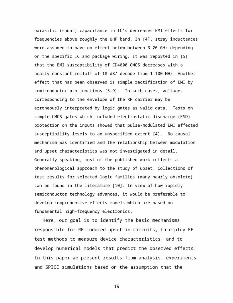
It has been widely reported that parasitic (shunt) capacitance in IC’s decreases EMI effects for
frequencies above roughly the UHF band. In [4], stray inductances were assumed to have no
effect below between 3-20 GHz depending on the specific IC and package wiring. It was reported
in [5] that the EMI susceptibility of CD4000 CMOS decreases with a nearly constant rolloff of 18
dB/ decade from 1-100 MHz. Another effect that has been observed is simple rectification of
EMI by semiconductor p-n junctions [5-9]. In such cases, voltages corresponding to the envelope
of the RF carrier may be erroneously interpreted by logic gates as valid data. Tests on simple
CMOS gates which included electrostatic discharge (ESD) protection on the inputs showed that
pulse-modulated EMI affected susceptibility levels to an unspecified extent [4]. No causal
mechanism was identified and the relationship between modulation and upset characteristics was
not investigated in detail. Generally speaking, most of the published work reflects a
phenomenological approach to the study of upset. Collections of test results for selected logic
families (many nearly obsolete) can be found in the literature [10]. In view of how rapidly
semiconductor technology advances, it would be preferable to develop comprehensive effects
models which are based on fundamental high-frequency electronics.
Here, our goal is to identify the basic mechanisms responsible for RF-induced upset
in circuits, to employ RF test methods to measure device characteristics, and to develop
numerical models that predict the observed effects. In this paper we present results from
analysis, experiments and SPICE simulations based on the assumption that the nonlinear
characteristics of p-n junctions and diode-like devices such as ESD protection circuits in
13

IC’s may be considered as RF detectors. As such, high frequency measurement
techniques and analysis have been employed to study the response of advanced logic
circuits to pulsed RF excitation. SPICE calculations were performed using models that
include packaging, bond wire and bypass capacitor parasitics; and nonlinear, high-
frequency device parameters obtained from both small and large-signal RF
measurements. This paper is organized as follows. In Section II, a small signal analysis of
RF detection by an ideal diode is presented along with calculations of the expected
rectified voltages. The high-frequency characterization of the ESD protection devices are
presented in Section III along with the measured transfer characteristics of a
representative sample of advanced CMOS families. Section IV includes a discussion of
the results and conclusions.
RF CHARACTERISTICS OF ESD DIODES Figure 1 shows some examples of ESD networks that are included in commercial
integrated circuits to protect them from damage during handling. Although there are
more complicated topologies not shown or discussed here, it is important to recognize
that they all contain nonlinear devices. These networks may rectify RF waveforms and
generate voltages which upset logic operation. In this chapter, a study of the high-
frequency characteristics of ESD diodes using the conventions and techniques of
microwave detector analysis will be presented. It will be demonstrated that ESD devices
have significant sensitivity to RF excitation even though they are not designed for this
purpose. Using the high-frequency characteristics of the diodes in SPICE models, it will
be shown that good agreement between experimental and numerical results is achieved
and that RF effects in circuits can be predicted with reasonable accuracy.
Figure 2a shows a generic CMOS gate which consists of the parasitic inductance
of the leads and bonding wire, the ESD diodes and the input transistors. If the input
logic voltage is within the normal range, both diodes are reversed biased and may be
considered as a constant junction capacitance as long as the RF excitation is small.
The circuit model is shown in Fig. 2b where the diode has been replaced by an equivalent
14

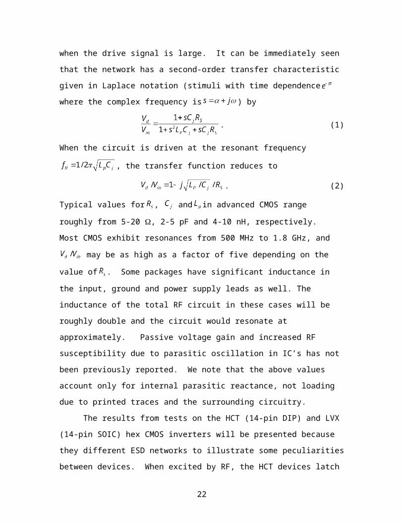
network including the current-spreading resistance and shunted by a video
resistance. For zero static bias, , where is the thermal voltage, is
the diode saturation current, is Boltzmann’s constant, is Kelvin temperature and is
the elemental electron charge. In the figure, and are shown as variable elements
because they both depend on the diode voltage and are therefore dynamic, nonlinear
quantities when the drive signal is large. It can be immediately seen that the network has
a second-order transfer characteristic given in Laplace notation (stimuli with time
dependence where the complex frequency is ) by
. (1)
When the circuit is driven at the resonant frequency , the transfer
function reduces to
. (2)
Typical values for , and in advanced CMOS range roughly from 5-20 , 2-5 pF
and 4-10 nH, respectively. Most CMOS exhibit resonances from 500 MHz to 1.8 GHz,
and may be as high as a factor of five depending on the value of . Some
packages have significant inductance in the input, ground and power supply leads as well.
The inductance of the total RF circuit in these cases will be roughly double and the circuit
would resonate at approximately. Passive voltage gain and increased RF susceptibility
due to parasitic oscillation in IC’s has not been previously reported. We note that the
above values account only for internal parasitic reactance, not loading due to printed
traces and the surrounding circuitry.
The results from tests on the HCT (14-pin DIP) and LVX (14-pin SOIC) hex
CMOS inverters will be presented because they different ESD networks to illustrate some
peculiarities between devices. When excited by RF, the HCT devices latch to the wrong
output state when their inputs are biased low but float to an undefined output voltage with
the input biased high. The LVX does the opposite. The reason for this difference has to
do with the various arrangements of ESD diodes. As shown in Fig. 1, diodes connected
from the input to either or both the ground and supply lines establish two basic pathways
15

for RF current. Complicating matters is the fact that the RF impedance of these paths is
dynamic. During normal operation, the junction biases would change constantly as valid
logic waveforms arrive at the inputs. Depending on the coincidence of an RF pulse with
respect to the logic voltage, the diodes will be driven at varying operating points along
their current-voltage (I-V) curves. We will not consider time-varying bias here; instead
the input will be held at a constant DC voltage consistent with the manufacturer’s
specifications input logic low ( ) and high ( ) voltages.
Once the high-frequency parametric curves and , and the constant
terms and are known for a given diode network, its sensitivity to arbitrary RF
excitation should be predictable. This hypothesis was tested in these two specific device
families (commercial HCT and LVX inverters) by measuring the DC and high-frequency
characteristics of the input diodes and constructing PSPICE models using the high-
frequency parameters extracted from the test data.
A. High-Frequency Characteristics of ESD Diodes
In the following, the experimental measurement of the diodes and how the
parameters were determined will be discussed. The devices were mounted on printed
circuit boards with their inputs fed by SMA-type RF connectors soldered as close as
possible to the input pins. The DC I-V characteristics of the input diodes were measured
using a conventional semiconductor curve tracer. Shown in Fig. 3 is a plot of the
experimental data compared to the ideal diode equation , where
n is an ideality factor related to the type and concentration of doping in the junction. The
high-frequency, complex input impedance was measured using an HP8722D vector
network analyzer (VNA) equipped with an internal bias network. The impedance was
digitally recorded while the frequency was swept between 50 MHz to 6 GHz and for bias
voltages between 0-3 V (the specified range of input logic voltage). The VNA averaging
function was enabled in order to eliminate noise and fluctuations in the measurements.
The data curves were fitted to the equation to obtain the
parameters , and m which are the zero-bias junction capacitance, the junction
potential, and the emission coefficient, respectively. Fig. 4 shows a comparison of the
16

measured and calculated capacitance versus bias voltage for the LVX inverter. The
inductance was measured resonant frequency. Also, the imaginary part of the impedance
(reactance) vanishes precisely at resonance, and the remaining real impedance gives the
value of the current-spreading resistance at high frequencies. A summary of the HCT
and LVX diode parameters is given in Table I.
B. Measured and Simulated Response of ESD Diodes to RF Excitation
The input response of the HCT and LVX inverters was measured as follows. Figure 5
shows a schematic of the test system including instrumentation, the RF path and points at which
voltage measurements were taken. A Stanford Research Systems DG535 pulse generator
supplied synchronization pulses to a digital oscilloscope and served as the modulation input to the
Agilent E4438C signal generator. The pulse width and repetition frequency were set to 10 µsec
and 100 Hz, respectively. The carrier frequency of the signal generator was tuned in each case to
the parasitic resonant frequency as dicussed above. A bias Tee, rendered in the figure as a
coupling capacitor on the RF port and a low-pass filter (LPF) on the bias port, was inserted into
the RF path between the generator and the device under test (DUT). RF was coupled into the
device as shown. The bias port served as the node at which DC voltages were applied and the
input response voltage was measured. The LPF served to block the carrier and pass low-
frequency signals which were down-converted off the carrier by diode rectification. A
bandwidth-limited representation of the response voltage was measured across a 10-kΩ resistor,
which also served to pull the DUT to the correct logic state. Figure 6 shows a typical input
response waveform when an RF pulse was applied to a CMOS device. It can be seen that the
ESD diodes produce a fairly good representation of the RF except for an inductive spike which is
generated by the diodes as the pulse terminates. The cause of the spike is related to the diode
recovery current interacting with parasitic inductance in the circuit. A detailed study of this
phenomenon will be presented in a future paper. As the carrier frequency was tuned across the
circuit resonance, a peak in the response voltage was observed as predicted by (1). The response
voltage of the HCT inverter was averaged over the flat portion of the pulse and digitally recorded
for each step in carrier amplitude between 20 mV and 1.0 V in 20 mV increments. We note that
below approximately 200 mV, no response was observed. This is a reasonable result since the
diode requires an RF voltage which exceed over some portion of its cycle in order to begin
rectifying. In the HCT, = 0.65 V which means that the voltage gain as defined in (2)
17

is about 3.25 in the resonant circuit. Substituting the HCT diode parameters, = 15 , =
5.8 pF and = 16 nH, into (2) yields a theoretical gain of 3.64, which is in good agreement with
the experimental value. The reason that the gain is slightly lower in the measurement is because
the capacitance decreases as the rectified voltage charges and reverse biases the junction. This
has two important effects on the circuit response. First, since the capacitance is dynamic, so is
the resonant frequency. Second, the quality factor (Q) of the circuit, which appeared implicitly in
(2) as where , means that the circuit response is dynamic as
well. Measurements were performed both with the 10-k resistor grounded and also fed from a
3.0 VDC voltage source to simulate device operation in both the low and high logic states,
respectively. The devices were powered using a regulated 3.3 VDC supply, and 0.2 µF ceramic
bypass capacitors were soldered as close as possible between the supply and ground terminals.
The measurements were repeated for the LVX device using RF amplitudes up to 1.4 volts for the
low bias case and 1.0 volt for the high bias case.
Table I. Diode parameters used for the lower and upper ESD diodes for HCT and LVX simulation circuits
18
The circuits were simulated using PSPICE with the high-frequency parameters given in
Table I applied to the diode models. Figure 6 shows the parasitic package inductance, the input
diffusion resistance, CMOS transistors arranged in triple-buffered configuration, the bias circuit
and the equivalent series resistance of the bypass capacitor. Transient analysis was performed
for the same range of RF amplitudes as in the experiments and with the inputs biased to both
and . The time necessary for the input response voltage to reach steady state in the simulation
was about 500 nsec, and the computation time on dual-processor workstation was approximately
two minutes. In Fig. 7, the results from measurements and simulations are compared, and good
agreement is demonstrated. Figure 8 and 9 show the circuit model and comparison of results,
respectively, for the LVX device. In this case, the agreement was also very good when the LVX
input was low and in the high state for RF amplitudes below 0.6 V. In the experimental data,
however, as the inverter is biased near its switching threshold, a sharp decrease in the input
response voltage is observed. This effect is caused by a feedback mechanism when both CMOS
transistors are biased into conduction (Miller Effect) and will be treated in a subsequent article.
We note that the CMOS transistors used in the simulations were unmodified library models. In
the future, a study of the high-frequency characteristics of CMOS will be conducted so that
improved transistor models may be included in the simulations. Nevertheless, the models give
fairly good agreement for most of the cases studied.
C. Dependence of RF Sensitivity on the Video and External Load ResistanceRecall that in the numerical and experimental circuits a value of 10 kΩ was
chosen for the input bias resistor purely based on bias and logic considerations.
Essentially, the above results give the RF transfer characteristics for a single, static load
condition. In reality, the inputs to CMOS devices are loaded by the preceding circuitry,
which itself changes states (output impedance) as the desired logic waveforms are
generated. Also, recall that the model of an RF detector diode (see Fig. 2b) includes
the dynamic video resistance which is essentially the inverse RF conductance of
the junction. This parameter depends on the high-frequency I-V characteristics of the
device which, in turn, determines its sensitivity to an RF voltage which can be
approximated by the Taylor series expansion around diode voltage given by
. (3)
19

In the above expansion, is the DC bias point, which in our case is the logic voltage
applied to the input, is the load impedance, and is the diode conductance. We
have expressed the load as an impedance to account for the general case where it may be
complex. In the following, we will assume that the load is purely resistive and solve (3)
using a small-signal approximation, namely, that the second derivative of the
conductance curve is reasonably constant over voltage excursions with amplitude .
The detected voltage for the case where following the analysis in [13] is
. (4)
The response voltage which is the measurable quantity is the drop across the external
load resistor where and is given by
. (5)
From (4) and (5) it can be seen why RF diodes are commonly called “square-law”
detectors since .
To test the validity of the analysis, the bias resistor in the experiments and
simulations was varied by decades from 100 to 1M and from 100 to 1Min 500
points, respectively. Figure 10 shows a plot of from theory (with the diode
parameters substituted into the relevant variables), simulations and the experiments
versus load conductance .
TRANSFER CHARACTERISTICS OF CMOS DRIVEN BY RF PULSES In the previous chapter, the behavior of ESD diodes was considered apart from the
operation of the circuit as a whole. Note that ESD protection is included in most IC’s
including some analog, mixed signal and virtually all digital circuits. The foregoing
analysis is applicable to a wide variety of devices and forms the basis for predicting RF
effects in IC’s in general. In this chapter, a study of the effects RF pulses have on the
operation of CMOS devices is presented. Before proceeding, it will be instructive to
20

briefly consider the special case when amplitude-modulated (AM) RF carriers are
rectified (detected) by diodes.
When junctions are excited by an AM carrier, rectification produces a voltage
which contains harmonics of the carrier frequency plus a reconstructed version of the
low-frequency AM signal. For the special case of steady-state sinusoidal modulation the
detected voltage after low-pass filtering is written
, (6)
where and m are the AM frequency and modulation index with the constraints
and 0<m<1, respectively. The spectrum of an RF pulse contains many
modulation sidebands. The above equation (6) is still valid as long as the contributions
from all the modulation frequencies are computed. Since rectification is a nonlinear
process, the diodes generate intermodulation products of the constituent AM frequencies
and harmonics of the carrier frequency, all of which appear at the CMOS gates. The
condition implies that the gate stimulus will occupy two distinct frequency
bands: 1) the modulation frequencies which are within the normal gain bandwidth of
CMOS transistors and 2) the RF frequencies which may be amplified or attenuated
depending of the high-frequency characteristics of the CMOS. Here, we will assume that
the demodulated waveform is the principal cause of upset in the device and measure the
response voltages over a bandwidth that encompasses the AM spectrum only. Note that
sometimes a remnant of the RF waveform with significant amplitude was visible at the
output of the device when time-averaging was removed and the measurement bandwidth
was increased.
The measurements of the HCT and LVX response were conducted as described
before using the test system shown in Fig. 5 with the carrier tuned to the parasitic
resonant frequency of the DUT. Since the oscillating current within the resonant circuit
is partly supplied by stored energy, the rectified voltage can be higher than predicted by
(6). As the RF amplitude was increased in 20 mV increments, the output voltage and
supply current was measured with the input biased to the low and high states. The input,
output and supply current waveforms were recorded by a digital oscilloscope using a
Tektronix P6243A probe across the 10-k input bias resistor and a Tektronix P6139A
21
probe across a 1.0-M resistor at the output terminal. The RF pulse width was 10 µsec
which gave adequate time for the response voltages to reach steady state before the pulse
terminated. To reduce noise and fluctuation in the data, the digitized voltages and current
were averaged over a time window of 5 µsec which was centered on the flat portion of
the pulse. The bandwidth of the voltage measurements was 20 MHz.
The experimental conditions were simulated using PSPICE to verify that the
circuit models of the ESD diodes and CMOS transistors gave reasonable predictions.
Transient analysis was performed for a simulation time of 6 sec using a step ceiling of
50 psec. The simulated RF-pulse width was narrower than in the measurements to save
simulation time. A comparison of the input and output response voltages versus time
from measurements and simulations of the HCT and LVX circuits in both bias states is
show in Figs. 11 and 12. Waveforms were recorded for RF amplitudes of 0.4 and 1.0
volts to demonstrate the cases where the input response voltage is above and below the
CMOS threshold voltage where the logic state changes. The complete data sets for the
HCT and LVX devices are shown in Figs. 13 and 14 represented as voltage and current
transfer curves versus RF amplitude.
In Fig. 13(a), the data for HCT response with its input biased low indicates that
RF amplitudes above 0.38 V cause the output to latch low. The abrupt spike in supply
current is consistent with normal operation in CMOS since both the NMOS and PMOS
transistors conduct when the input voltage is near the switching threshold. Evidently, the
envelope voltage from the rectified RF pulse has mimicked a valid logic waveform and
induced a state error in the device. A more subtle effect is the elevated leakage current of
about 1 mA for RF amplitudes higher than about 0.4 volts. This result indicates that not
all the transistors are completely latched in their respective states. Rather, a high-
frequency current continues to flow through the source-drain channel of the input buffer
and possibly the second gain stage. In Fig. 13 (b), the data shows that biasing the HCT
high produces a very different result. In this case, the bias condition forces the RF
current to flow through the (upper) diode with its anode connected to the input through a
diffusion resistance and the cathode to the power bus. The impedance of this network is
higher and, as previously discussed, the dynamic capacitance is different which means
that the resonant frequency and response characteristics have been altered by the bias.
22

We note that the RF carrier in all the measurements was tuned to the zero-bias resonant
frequency. Nevertheless, the RF still causes the output voltage to rise slightly meaning
that the output transistors are biased towards conduction. The current transfer
characteristic is very nonlinear around RF amplitudes of about 0.65 volts.
The data in Figs. 14 (a) and (b) show that the LVX has a much smoother transfer
curve and that state errors occur only with the input biased high and RF amplitudes above
approximately 1.35 V. When the input is biased low, the RF causes the output transistors
to partially conduct as evidenced by the minima in voltage and maxima in the current
curves at around 1.2 V of RF drive. Figure 15 illustrates the mapping of measured input
and output responses versus excitation amplitude and frequency. It can be observed that
the voltage-dependence of the junction capacitances causes an upshift in the resonant
response. Since the rectified voltage has a nonzero mean, it constitutes a new bias
condition which decreases the junction capacitance. Thus, excitation at frequencies
significantly above the zero-bias resonance still produces substantial gain and increases
the likelihood of upset over a fairly wide bandwidth.
DISCUSSION AND CONCLUSIONS
Concerning the accuracy of the numerical models, a major drawback was not
having the ability to measure the high-frequency characteristics of the MOS devices and
implement those parameters in the model. In lieu of this information, the transistors were
modeled using Level 4 SPICE models based on 1.2 um MOSIS MOSFETS with
characteristics that accurately predict their behavior when the stimulus is a normal logic
waveform. The models have not been tested when the input excitation consists of
combinations of DC, AM, carrier harmonics and inter-modulation products. The data
demonstrates that the transistor models do not predict some of the effects that have been
observed in the experiments. In future work, high-frequency measurements will be
performed on unpackaged CMOS transistors in order to evaluate which parameters are
lacking or require modification in the circuit models.
The response of the HCT and LVX CMOS inverters to pulsed RF excitation has
been studied where effects are caused by rectification of the RF by ESD protection
diodes. The high-frequency characteristics of the diodes have been measured and
23

successfully implemented in SPICE models, which have been shown to predict the RF
transfer curves of the diodes. The dynamic nature of the circuit parameters and their
importance with respect to circuit response has been discussed, calculated and compared
with experimental results with good agreement. Passive gain due to parasitic oscillations
in the input networks has been shown to increase susceptibility when devices are excited
near and above their zero-bias resonant frequency. In the HCT experiments, a passive
gain of 3.25 was demonstrated which compared favorably to the theoretical value of 3.64.
Finally, the output voltage and current transfer curves have been measured, and the
conditions leading to logic-state errors, partial conduction and excess current draw have
been studied and characterized.
REFERENCES
[1] M. L. Forcier and R. E. Richardson, Jr., “Microwave-rectification RFI response in
field-effect transistors,” IEEE Trans. Electromag. Compat., vol. EMC-21, no. 4, Nov.
1979.
[2] K. Gong, H. Feng, R. Zhan, and A. Z. H. Wang, “A Study of Parasitic Effects of
ESD Protection on RF ICs,” IEEE Trans. Microwave Theory and Techniques, Vol.
50, No.1, January 2002.
[3] D. J. Kenneally, D. D. Wilson, and S. Epshtein, “RF upset susceptibilities of CMOS
and low power Schottky 4-Bit magnitude comparators”, 1990 IEEE Int. Symp. On
Electromag. Compat., Wash. DC, 21-23 Aug. 1990, pp. 671-677.
[4] D. J. Kenneally, D. S. Koellen, and S. Epshtein, “RF upset susceptibilities of CMOS
and low power Schottky D-Type, Flip Flops,” Rec. 1989 IEEE Nat. Symp.
Electromag. Compat., Denver, CO, 23-25 May, 1989, pp. 190-195.
[5] D. J. Kenneally, G. O. Head, and S. C. Anderson, “EMI noise susceptibility of ESD
protect buffers in selected MOS devices,” Procs. IEEE Int. Conf. on Electromag.
Compat., Wakefield, MA, August 1985, pp. 251-261.
[6] R. Richardson, “Microwave rectification of RFI in logic circuitry,” NBS Conf.
Microelectronics and Electromag. Susceptibility, Gaithersburg, MD, 12-13 Mar.,
1985.
[7] R. E. Richardson, Jr., “Quiescent operating point shift in bipolar transistors with AC
24

excitation,” IEEE J. Solid-State Circuits, vol. SC-14, no. 6, Dec. 1979.
[9] S. D. Le Vine and R. E. Richardson, “Measurement techniques and instrumentation
for determining sensitivity of digital IC’s to radio-frequency interference,” Proc.
ITMC/86, IEEE Instrum. Meas. Tech. Conf., Boulder CO., March 25-27, 1986.
[10] J. N. Roach, “The susceptibility of a 1k NMOS memory to conducted
electromagnetic interference,” Rec. 1981 Nat. Symp. Electromag. Compat. Symp.,
Boulder, CO, Aug. 1981, pp. 85-90.
[11] G. Sketoe, “Integrated Circuit Electromagnetic Immunity Handbook”, Boeing
Information, Space and Defense Systems, Seattle, WA, August 2000.
[12] Albert Z. H. Wang, On-chip ESD Protection for Integrated Circuits. Norwell, MA:
Kluwer, 2002.
[13] J. J. Whalen, J. G. Tront, C. E. Larson and J. M. Roe, “Computer aided analysis of
RFI effects in digital integrated circuits,” IEEE Trans. Electromag. Compat.,
vol. 21, pp. 291-297, Nov. 1979.
[14] D. M. Pozar, Microwave Engineering, 2nd ed., New York, NY: J. Wiley & Sons,
1998.
FIGURES FOR SECTION III.2.b
Fig. 1 Four examples of ESD protection circuit topologies: (a) ground to signal ESD
diode, (b) diffused resistance and signal to Vdd ESD diode, (c) gate grounded
NMOS and PMOS, and (d) zener topology with two diodes from ground to signal
separated by a diffused resistor and back to back zeners from signal to Vdd.
Fig. 2 Block diagram of (a) the input to a CMOS inverter including parasitic inductance
(Lp), ESD protection diodes and an inverter stage and (b) simple model for ESD
protection diode modeled as a voltage dependent junction capacitance (Cj),
voltage dependent video resistance Rv, and current spreading resistance (Rs).
25

Fig. 3 The measured I-V characteristics of ESD diodes from ground to signal lines for
the HCT and LVX inverters fit to the ideal diode equation to determine saturation
current (Is) and emission coefficient (n).
Fig. 4 Junction capacitance measured using a HP 8722D VNA and calculated for the
ESD protection diode from ground to signal line in the LVX CMOS inverter fit to
the voltage dependent junction capacitance to determine (Cj0) and the p-n grading
coefficient (m).
Fig. 5 Block diagram for circuit used to measure the rectified input and resulting output
voltage for the 74HCT04. A Stanford Research Systems DG535 was used as an
external pulse source for the Agilent E4438C Vector Signal Generator. The RF
pulses were capacitively coupled to the input of the 74HCT04 for the injection
experiments. A 100 MHZ low-pass filter (LPF) was used to measure the low-
frequency rectified voltage at the input of the HCT CMOS inverter via a
Tektronix TDS 540C oscilloscope. The same oscilloscope also captured the time
domain waveforms of the RF envelope pulse and the output voltage.
Fig. 6 PSPICE circuit diagram of the CMOS inverter used to simulate the drive curve
and time domain waveforms of a HCT CMOS inverter. The ESD protection
topology consists of two diodes separated by a diffusion resistor. The low-
frequency rectified voltage was monitored through the low-pass network.
Fig. 7 The measured input drive curve for the HCT CMOS inverter when a low bias
voltage (0.0 volts) and high bias (3.0 volts) were applied which was fit to the
simulated drive curve in the circuit of Error: Reference source not found.
Fig. 8 PSPICE circuit diagram of the CMOS inverter used to simulate the drive curve
and time domain waveforms of a LVX CMOS device. The ESD protection
topology consists of a diode from signal to ground and a diode from signal to
26

Vdd. The low-frequency rectified voltage was monitored through the low-pass
network.
Fig. 9 The measured input drive curve for the LVX CMOS inverter when no bias
voltage was applied which was fit to the simulated drive curve in the circuit of
Error: Reference source not found.
Fig. 10 Plots of the measured and simulated detected voltage versus load conductance for
the LVX and HCT CMOS inverters.
Fig. 11 The measured rectified voltage at the input when no bias voltage was applied with
the resulting output voltage (a) simulated and (b) measured on the 74HCT04
inverter. Input and output voltages are shown for RF amplitudes of 400 mV and 1
volt.
Fig. 12 The measured rectified voltage at the input when a bias voltage of three volts was
applied with the resulting output voltage (a) simulated and (b) measured on the
74HCT04 inverter. Input and output voltages are shown for RF amplitudes of 400
mV and 1 volt. No state change was observed at the output in either case.
Fig. 13 Complete mapping of measured 74HCT04 inverter response versus the amplitude
and frequency of pulsed RF excitation. The shading of the vertical scale indicates
the fractional deviation in output voltage from the valid logic level.
Fig. 14 Map of measured 74LVX04 inverter response versus the amplitude and frequency
of pulsed RF excitation.
27

Fig. 1
28

(a)
(b)
Fig. 2
29

(a)
(b)
Fig. 3
30

Fig. 4
31

Fig. 5
32

Fig. 6
33

Fig. 7
34

Fig. 8
35

Fig. 9
36

Fig. 10
37

(a)
(b)
Fig. 11
38

(a)
(b)
Fig. 12
39

Fig. 13
40

Fig. 14
III.2.c Experimental Studies of Pulsed RF Interference on IC
41

MOSFETs, Inverters, and Differential Amplifiers.
This project focuses on identifying the effects of microwave power signals on the fundamental units of integrated circuits (IC’s) such as individual MOSFETs, CMOS inverter gates, and elemental differential amplifiers. Furthermore it seeks to develop microwave hardened chips by identifying the vulnerabilities of the elemental IC units and re-designing units accordingly, and introducing on-chip protection using nanocomposite coatings. In this past year we have designed and fabricated Si wafers with individual n channel enhancement mode MOSFETs and inverters and examined the effects of injected microwave pulsed power signals on the operational DC and small signal parameters of the device with microwave power and frequency. Emphasis was placed in identifying specific effects caused by the microwave events that render the devices inoperable or outside the operational parameters of the interconnected units thus resulting in “soft” and “hard” errors. The CMOS inverters were designed and fabricated in AMI-1.5um MOSIS technology with sizes for the NMOS and PMOS transistors of W/L=3.2/1.6um and 9.6/1.6um respectively, in packaged and unpackaged form. Pulsed microwave signals were injected at the inputs and outputs of individual MOSFETs and inverters and the operational parameters examined. Measurements on individual MOSFETs (Fig. 1) showed that injected pulsed microwave power significantly affected output voltages for power levels above 20 dBm between 1 and 4 GHz, and resulted in increased drain currents in the saturation region, and DC offset currents at zero drain bias, while the power effects were observed to be suppressed at the higher end of the microwave frequencies (3-4 GHz) as shown in Fig. 2, 3 and 4. Microwave pulses injected at the inputs and outputs of individual inverters (Fig. 5) revealed for the first time that at power levels at or above 22dBm at frequencies of 1-3 GHz the parasitic bipolar transistor action (latch-up) can be activated making the devices inoperable and in need to be reset to function again (Fig. 6 and 7). Further study showed that the operational parameters of the inverters were substantially affected by the RF signals to the extent that the units were by far outside their set operational limits giving “bit flipping” errors. Furthermore, significant degradation in the voltage and current transfer characteristics, the inverter operational point, the inverter gain, the input output voltages (VOH, VOL, VIL, VIH), the noise margins, and substantial power dissipation increase, were observed (Fig. 8 and 9), indicating severe non-functionality when the unit is interconnected with other units in a digital chip. Our studies of individual MOSFETs [1] showed that the application of RF interference resulted in the inability of the MOSFET to switch off the channel, indicating substantially higher carrier densities created by the RF events. The channel reaches no “pinch-off” due to the high densities of these excess carriers which forward bias the source junction with the p-type substrate thereby activating the parasitic bipolar transistor and resulting in the observed latch-up in the p-substrate-n-well CMOS structure.
Our continuing study will examine the physical mechanisms responsible for the observed pulsed microwave interference effects, examine their relative importance, in terms of electronic transport processes (effective mobility changes, capacitance changes, gain
42

degradation, parasitic and short channel phenomena, oxide degradation, doping profile degradation, response and switching speed), processes of creation of excess carriers, and thermal processes (self heating effects, thermally generated carriers, and increases in carrier temperature under high fields). Based on the experimental evidence we are developing a theoretical framework of equations to include these effects in order to provide the basis for re-designing these devices for improved microwave interference hardness.
REFERENCES:[1] K. Kim, A.A. Iliadis and V. Granatstein, “Effects of microwave interference on the operational parameters of n-channel enhancement mode MOSFET devices in CMOS integrated circuits”, Solid State Electronics 48, (2004) pp.1795-1799.
Fig. 1. RF injection to gate measurement set-up. Output measured at point indicated by the arrow.
43
G D
S, B
B
W=30m L=20m
Bias T
VRF
VG
VDD
R=180kΩR=470Ω
R=470Ω
0 10 20 30 40 506.7
6.9
7.1
7.3
7.5
7.7
1GHz 30dBm4GHz 30dBm
VDS
(V)
Time (μs)

Fig. 2. Output VDS after pulse injection to gate. MOSFET DC bias conditions: VG=6V, VDD=8V, VDS=7.6V, VGS=5.6V (saturation region). VDS lowered from 7.6V to 6.7V thus increasing output current IDS. Increased pulse envelope frequency results in suppressing the effects of power: 1GHz to 4GHz at 30dBm.
Fig. 3. Zero bias conditions (Gate and Drain) and 1GHz 30dBm RF pulse injection to Gate, the output Drain voltage is negative causing positive IDS to flow at the output at zero bias.
44
0 10 20 30 40 50-0.25-0.2
-0.15-0.1
-0.050
0.05
VDS
(V)
Time (μs)
0 5 10 15 204.5
4.6
4.7
4.8
4.9
1GHz 20dBm1GHz 30dBm
VDS
(V)
Time (μs)

Fig. 4. Pulse injection to Drain in Saturation: Drain voltage VDS decreases, hence IDS increases with RF power increasing. RF Pulse: 1GHz, 9μs pulse width.
Fig. 5. RF injection to Inverter Gate measurement set-up. Output measured at point indicated by the arrow for the first inverter.
45
VDD
R=180KΩ
BiasT
Vinput
R=470ΩVRF
Amp
VPulse
VO
0 1 2 3 4 50
1
2
3
4
5RF EnvelopeOutputOutput Latched
VO
(V)
Time (μs)

Fig. 6. Input RF pulse has 800ns width, 10ms period. At 20 dBm and 1.23 GHz the inverter output state changes from high to low. At 22.45dBm and frequency 1.23GHz, with input state low (0V), output of inverter (1) shows gradual decrease until complete latch-up is observed at 1.24V and the inverter needs to be reset to be operational again.
Fig. 7. At input logic state high (5V DC). The output DC level increases as RF power increases. At 23.25dBm, the CMOS inverter experiences latch-up of output to 1.24V. Device bias (VDD) needs to be reset to get normal operation again.
46
0 1 2 3 4 50
0.5
1
1.5
2
2.5RF EnvelopeOutputOutput Latched
VO
(V)
Time (μs)
-0.05
0
0.05
0.1
0.15
0.2
0.25
-5 0 5 10
VIN (V)
I (m
A)
DC1GHz 0dBm1GHz 15dBm1GHz 24dBm

Fig. 8. Inverter current transfer characteristic measurement with 1GHz RF injection at gate. Substantial output current increase with RF power is observed.
Fig. 9. Inverter voltage transfer characteristic measurement with 1GHz RF injection at gate. Substantial degradation in gain, noise margins, and Hi-Lo voltage points with RF power is observed.III.3 Fabrication and Testing of On-Chip Microwave Detectors(Professor John Melngalis, Dr. John Rodgers;
47
0
1
2
3
4
5
6
0 1 2 3 4 5
VIN (V)
VO
(V)
DC1GHz 0dBm1GHz 15dBm1GHz 24dBm

Students: Todd Firestone, Woochul Jeon)
The overall goal of this project is to develop and build RF detectors that can be located on various parts of a chip so that when a given circuit or instrument is irradiated the level of RF picked up in that chip can be measured. This will provide more information than the simple "yes/no" provided by detecting only circuit failure. We can also envisage building packaged RF detector test chips which have the same electromagnetic characteristics and the same connections to the rest of a circuit as a particularly vulnerable chips in a system. The test chips can then be substituted in the circuit for the vulnerable chips and can be used to measure the RF level picked up in the circuit under various pulsed RF conditions and various external system configurations.
Previously report Schottky diodes were built by a CMOS compatible fabrication process and by a post-CMOS fabrication process using focused ion beam(FIB) milling and FIB induced deposition. These diodes operated up to 12GHz (in some cases higher) when irradiated by direct injection or by irradiation "through the air". In this reporting period we concentrated less on high frequency (though we achieved high frequency operation anyway) but rather on increasing sensitivity, building transistor based detectors, and on minimizing the loading on the circuit by the RF detector.
Although we knew from previous tests that making Schottky diodes in a MOSIS process was difficult, we tried again since the processes were newer and since it did not cost much chip area or effort to do so on chips we were making for this project anyway. We have tested possible contacts, such as metal to n-well contact, on AMIS 1.5, 0.5, CMOS process and, unfortunately, failed to achieve Schottky diode characteristics. Most of these contacts were ohmic (or very poor diodes). For the AMIS 0.35 process we measured good Schottky diode characteristics on n-type material in some cases.
As a post CMOS process, FIB milling and ion induced deposition was used to build Schottky diodes on a CMOS chips fabricated by the AMIS 0.5µ CMOS process. These Schottky diodes were tested up to 15GHz and showed dynamic range of 30dBm. The RF pulse response time were 100 nsec to 2 sec. There is a trade-off between RF pulse response time and output voltage, i.e. smaller area yields faster response but lower rectified output voltage.
As an alternative CMOS power detector design, MOSFET detectors were designed and tested up to 20GHz and detected –15dBm to 10dBm RF pulses. To examine the effect of adding power detectors to a logic circuit, AND/OR logic circuits with power detectors were simulated. Diode detectors altered the logic output and MOSFET detectors gave much smaller effects on the logic circuit operation due to the high impedance in the MOSFET detector.
48

Fig. 1. Output voltage from the detector circuit with a 150kohm load as a function of input power (top) and frequency (bottom). The power level quoted is the level delivered to the Cascade probe. A non-optimized transmission line connects the probe pads to the detector circuit. The loss in this transmission line is known to increase strongly with frequency. Thus the decrease in output voltage with frequency may be largely due to this effect rather than an inherent property of the detector.
As future work, another FIB Schottky diode, which has smaller series resistance, will be fabricated and tested. And to know how our detectors pick up radiated RF pulse, packaged and un-packaged detectors will be tested under RF pulse radiation. To increase the sensitivity and the dynamic range of MOSFET detectors, another MOSFET detector was designed to adjust turn-on-voltage to 0V and a full-wave rectifier circuit was also conceived and simulated. These circuits will be fabricated in December.
III.4 Studies of Enclosures and Shielding ( Professor Omar M. Ramahi. Students who have graduated: Lin LI, Xin Wu, Baharak Mohajer-Iravani. Current Students: Sharooz Shaparia, Mohanmmad Haeri Kermani)
49
Frequency sweep at 0 and 5dBm
1.0E-04
1.0E-03
1.0E-02
1.0E-01
1.0E+00
0 5 10 15 20
Frequency (GHz)
Vout
(V)
Vo at 0dBmVo at 5dBm
Power sweep at 1, 3, 5GHz
0.001
0.01
0.1
1
-20 -15 -10 -5 0 5 10Pow er level (dBm)
Vout
(V) Vo at 1GHz
Vo at 3GHzVo at 5GHz

III.4.1 Electromagnetic Interference (EMI) Reduction from Printed Circuit Boards (PCB) using Electromagnetic Bandgap Structures
As digital circuits become faster and more powerful, direct radiation from the power bus of their printed circuit boards (PCB) becomes a major concern for EMC engineers. In such multilayer PCBs, the power and ground planes act as radiating microstrip patch antennas, where radiation is caused by fringing electric fields at board edges. In this work, we introduced an effective method for suppressing PCB radiation from their power bus over an ultra wide range of frequencies by using metallo-dielectric electromagnetic band-gap (EBG) structures. More specifically, this study focuses on the suppression of radiation from parallel-plate bus structures in high-speed printed circuit boards caused by switching noise, such as simultaneous switching noise (SSN), also known as Delta-I noise or ground bounce. This noise consists of unwanted voltage fluctuations on the power bus of a PCB due to resonance of parallel-plate wave-guiding system created by the power bus planes. The techniques introduced here are not limited to the suppression of switching noise and can be extended to any wave propagation between the plates of the power bus. Laboratory PCB prototypes were fabricated and tested revealing appreciable suppression of radiated noise over specific frequency bands of interest, thus testifying to the effectiveness of this concept.
Miniaturized EM Bandgap Structures for Ultra-Wide SwitchingNoise Mitigation in High-Speed Printed Circuit Boards and Packages In this work, a novel design for electromagnetic bandgap structures embedded in packages is introduced. This design is able to mitigate switching noise in a power distribution network on an unprecedented range of frequencies, while having a very compact, miniaturized and practical structure. The backbone of this technique involves using high dielectric permittivity material.
Simultaneous Switching Noise Mitigation in High Speed Printed Circuit Boards (PCB) using Cascaded High-Impedance Surfaces Simultaneous switching noise (SSN) is an induced voltage glitch on the Power Distribution Network (PDN) of chips and packages generated when internal circuits in digital gates as well as their output drivers switch simultaneously. In our research, a novel design method for the ultra wide bandwidth suppression of simultaneous switching noise in high-speed printed circuit boards (PCB) is proposed and implemented. This method consists of cascading different configurations of High-Impedance Surfaces (HIS) with different stop-bands, thus creating rejection over a wider frequency range. Current SSN suppression methods rely on using discrete decouplingcomponents, RC edge terminations, dissipative material on the edges of the PCB, and also embedded capacitances. The design presented in our work not only exceeds the amount of suppression achieved by these methods but also overcomes two of their most critical limitation:cost and bandwidth.
Practical Considerations in the Design and Fabrication of Electromagnetic Band Gap Structures Current designs that employ High-Impedance Surfaces (HIS) in multilayer Printed Circuit Boards (PCB) use blind and buried vias, which are costly and require special manufacturing technologies. In addition, the thickness of the designed PCBs is not in the range of practical
50

manufacturing values. This work studies the effect of board thickness variation on the behavior of HIS surfaces, therefore extending already available design methodologies to practical applications. In addition it studies the effect of eliminating blind and buried vias in such designs. By extending the vias to the other metallic power plane and eventually to the outmost layers of the board, HIS structures can be implemented using inexpensive PCB technologies that support only through-hole vias. Results.
Coating Apertures to Reduce Aperture Resonance In this work, we propose the use of resistive sheets to improve the shielding effectiveness of enclosures with apertures. It is found that significant reduction of electromagnetic leakage is possible by using loading techniques inspired by the transmission line interpretation of current distribution on apertures at the resonance frequency of the aperture. Results form numerical simulations as well as from laboratory measurements are presented to validate the concept presented here.
Multiband Mitigation using Mixed Topology Electromagnetic Band Gap Structures A novel electromagnetic band-gap structure (EBG), whose surface impedance is primarily controlled by its inductance per unit area, is presented. This EBG, which exhibits two wide forbidden band-gaps at very low frequencies, is applied to mitigating resonant modes in parallel-plate waveguides. It is shown that the two forbidden band-gaps can either be controlled independently by varying the physical separation between adjacent patches or simultaneously by varying the number of turns of the spiral inductor used in the patch of the unit cell.
Simple and Accurate Circuit Models for High-Impedance Surfaces Embedded in Printed Circuit Boards Electromagnetic Bandgap Structures (EBG) have been employed to suppress Simultaneous Switching Noise (SSN) generated between power busses of printed circuit boards (PCB). EBG structures, when embedded in a PCB, can suppress electromagnetic wave propagation within a predictable range of frequencies. In this work, a highly-accurate model for HIS structures embedded in PCB’s is presented. This circuit is then added to a physics-based model for power busses of PCB’s, creating a compact 3D model to represent the power bus together with Embedded HIS (EHIS) structures. The circuit models presented allow for accurate prediction of the center frequency and bandgap of the EHIS without a priori full-wave modeling of a singe or multiple cells.
EM Surface Wave Mitigation to Reduce Coupling between Cavities Electromagnetic Interference (EMI) in electronic devices is one of the majorchallenges in the design of high-speed electronic packages. These challenges areintensified by the increase in the level of system integration and the ever increasingoperating frequency of microprocessors. EMI takes place at different levels including the package, board, component and chip. The physical mechanism behind electromagnetic interference is the coupling of energy between different components within the package or chassis. This coupling can be either conducted or radiated. However, regardless of the coupling mechanism, surface currents are needed to support the field that eventually radiate, which constitute the electromagnetic interference in the first place. Minimizing these surface currents is considered a fundamental and critical step in minimizing EMI. In
51

this work, we address novel strategies to confine surface currents. Unlike the traditional use of lossy materials and absorbers, which suffers from considerable disadvantages including mechanical and thermal reliability leading to limited life time, we consider the use of elctromagnetic Band Gap (EBG) structures which are inherently suited for surface current suppression. The effectiveness of the EBG as an EMI suppresser will be demonstrated using numerical simulations and experimental measurements.
IV. PERSONNEL SUPPORTED
IV.1 Academic Faculty
Professor Steven Anlage, Physics
52

Professor Thomas M. Antonsen, Jr., Physics and Electrical Engineering
Professor Neil Goldsman, Electrical Engineering
Professor Agis Iliadis, Electrical Engineering
Professor Bruce Jacob, Computer Engineering
Professor John Melngalis, Electrical Engineering
Professor Edward Ott, Physics and Electrical Engineering
Professor Omar Ramahi, Mechanical Engineering
IV.2 Research FacultyDr. Yuval Carmel, Inst. for Research in Electronics & Applied Physics (IREAP)
Dr. John Rodgers, IREAP
IV.3 Graduate StudentsVincent Chan Lin Li (graduated with Ph. D.)
Cagdas Dirik Baharak Mohajer-Iravani (Graduated with M.S.)
Todd Firestone Laise Parker
James Hart Shahrooz Shaparnia
Sameer Hemmady Xin Wu (graduated with Ph. D.)
Woochul Jeon Bo Yang
Mohammad Haeri Kermani X. (Henry) Zheng
Kyechong Kim
V. PUBLICATIONS AND PATENTS
V.1 Refereed Journal Papers During the Reporting Period
1. K. Kim, A. A. Iliadis, V. Granatstein, “Effects of microwave interference on the
53

operational parameters of n-channel enhancement mode MOSFET devices in CMOS integrated circuits”, Solid State Electronics, 48 (2004) pp. 1795-1799 (2004).
2. Renato Mariz de Moraes and Steven M. Anlage, “Effects of UHF Stimulus and Negative Feedback on Nonlinear Circuits,” IEEE Trans. Circuits Systems I v. 51 (2004) pp.748-754
3. Renato Mariz de Moraes and Steven M. Anlage, “Unified Model, and Novel Reverse Recovery Nonlinearities, of the Driven Diode Resonator,” Phys. Rev. E 68 (2003) paper 026201 (9 pages)
4. W. Jeon, T.M. Firestone, J.C. Rodgers and J. Melngalis, “Design and fabrication of Schottky diode on-chip RF power detector”, Solid State Electronics 48 (2004) 2089-2093
5. S. Shahparnia and O.M. Ramahi, “ Simultaneous switching noise mitigation in PCB using cascaded high-impedance surfaces” , Electronics Letters 40 (2004) paper 20040077 (2 pages)
V.2 Papers Submitted to Refereeed Journals
1. Sameer Hemmady, Xing Zheng, Edward Ott, Thomas M. Antonsen, and Steven M. Anlage, “Universal Impedance Fluctuations in Wave Chaotic Systems,” submitted to Physical Review Letters, 26 December, 2003.
2. X. Zheng, T.M. Antonsen Jr. and E. Ott, “Statistics of Impedance and Scattering Matrices in Chaotic Microwave Cavities: Single Channel Case”, submitted to Electromagnetics.
3. X. Zheng, T.M. Antonsen Jr. and E. Ott , “Statistics of Impedance and Scattering Matrices of Chaotic Microwave Cavities with Multiple Ports”, submitted to Electromagnetics.
4. W. Jeon, T.M. Firestone, J.C. Rodgers and J. Melngalis, “ On- RF pulse power detector using FIB as a post CMOS fabrication process “, submitted to Microelectronics Journal.
6. S. Shaparnia and O. Ramahi, “Electromagnetic Interference (EMI) Reduction from Printed Circuit Board”, IEEE Trans. Electromagnetic Compatibility (to be published Dec. 2004)
54

V.3 Papers Published in Conference Proceedings
1. Thomas M. Antonsen, Xing Zheng, Edward Ott, Sameer Hemmady, and Steven Anlage, “Statistical Model for Scattering Matrices of Open Cavities,” URSI
EMTS 2004, (2004) 825-827
2. K. Kim, A. A. Iliadis, V. Granatstein, “Effects of microwave interference in CMOS integrated circuits.” Proc. International Semiconductor Devices Research Symposium (2003) 530-531.
3. A. A. Iliadis, K. Kim, V. Granatstein, “Study of the effects of microwave interference on MOSFET devices in CMOS integrated circuits.” Proc. URSI-EMTs, Pisa, Italy, Vol II (2004) 819-821. Invited.
4. X. Shao, N. Goldsman, O. M. Ramahi, P. N. Guzdar, “A New Method for Simulation of On-Chip Interconnects and Substrate Currents with 3D Alternating Direction-Implicit (ADI) Maxwell Equation Solver,” International Conference on Simulation of Semiconductor Processes and Devices, pp. 315-318, 2003.
5. X. Shao, N. Goldsman, and O. M Ramahi, “The Alternating-Direction Implicit Finite-Difference Time-Domain (ADI-FDTD) Method and its Application to Simulation of Scattering from Highly Conductive Material,” IEEE International Antennas and Propagation Symposium and USNC/CNC/URSI North American Radio Science Meeting: URSI, Digest, p. 358, 2003.
7. Y. Bai, Z. Dilli, N. Goldsman and G. Metze, “Frequency-Dependent Modeling of On-Chip Inductors on Lossy Substrate,” International Semiconductor Device Research Symposium, pp. 292-293, 2003.
7. X. Shao, N. Goldsman, O. M. Ramahi,and P. N. Guzdar, “Modeling RF Effects in Integrated Circuits with a New 3D Alternating-Direction-Implicit Maxwell Equation Solver,” International Semiconductor Device Research Symposium, pp. 532-533, 2003.
8. Hongxia Wang, Cagdas Dirik, Samuel V. Rodriguez, Amol V. Gole and Bruce Jacob, “ Radio frequency effects on the clock networks of digital circuits." , Proc. IEEE International Symposium on Electromagnetic Compatibility (EMC
55

2004). Santa Clara CA, August 2004. 9. S. Shahparnia and O. Ramahi, “Simultaneous switching noise in high speed printed circuit boards (PCB) using cascaded high-impedance surfaces”, Proc. Microwave and Circuits Symposium, Cairo, Egypt, Dec. 2003
10. S. Shahparnia and O. Ramahi, “Ultra wide-band electromagnetic interference (EMI) reduction from printed circuit boards (PCB)”, Proc. Applied Computational Electromagnetic Society Annual Symposium, Syracuse, NY, April 2004
11. S. Shahparnia, O. Ramahi and B. Archambeault, “Design considerations for high impedance surfaces embedded in printed circuit boards”, ibid.
12. O. Ramahi and S. Shahparnia, “Novel concepts for noise mitigation in high-speed boards and packages using metallo-dielectric electromagnetic bandgap material – theory, simulation and measurement”, Proc. EMC’04, Sendai, Japan, June 2004
13. O. Ramahi and L. Li , “Controlling aperture resonance using novel coatingTechniques, theory, simulation and measurements”, ibid.
14. O. Ramahi, S. Shahparnia, and B. Mohajer-Irvani, ‘Towards new paradigms in noise mitigation in and from printed circuit board using metallo- dielectric electromagnetic band gap”, Proc. EMC’04, Eindhoven, The Netherlands, Sept. 2004
15. T. Kamgaing and O. Ramahi, “Electromagnetic band-gap structures for multi-band mitigation of resonant modes in parallel plate waveguides”, Proc. IEEE Antennas and Propagation Soc. Meetings, June 2004
16. B. Mohajer-Iravani and O. Ramahi, “New EMI shielding approaches using electromagnetic bandgap structures”, ibid.
17. S. Shahparnia and O. Ramahi, “High impedance surfaces embedded in printed circuit boards: design considerationa and novel applications”, ibid. 18. S. Shahparnia and O. Ramahi, “Simple and accurate circuit models for high impedance surfaces embedded in printed circuit boards”, ibid.
19. S. Shahparnia, B. Mohajer-Iravani and O. Ramahi, “Electromagnetic noise mitigation in high speed printed circuit boards using electromagnetic bandgap structures”, ibid.
56

20. A.A.Iliadis, K.Kim and V. Granatstein, “Effects of microwave interference onMOSFET devices in integrated circuits”, Proc. Sixth Annual Directed Energy Symposium”, Albuquerque, NM, 2003, p. 932
V.4 Patents
1. A. Iliadis, “Sense and Protect Circuit”: US Patent Pending # MR2833-15.
VI. INTERACTIONS / TRANSITIONS
VI.1 Presentations at Meetings and Conferences
57

1. V. L. Granatstein, “RF Effects and Chaos in Integrated Electronics”, DEPS HighPower Microwave Conference, Aug. 17, 2004, Kirtland AFB, Albuquerque, NM
2. Rodgers, T. M. Firestone, V. L. Granatstein and S. Anlage, “Radio-Frequency
Effects in CMOS with Electrostatic Discharge Protection,” poster paper, ibid.
3. John Rodgers, T. M. Firestone, V. L. Granatstein, E. Ott, T. M. Antonsen, Jr., S.
Anlage, O. Ramahi and N. Goldsman, “Radio-Frequency Effects in CMOS with
Electrostatic Discharge Protection,” John Rodgers, T. M. Firestone, V. L. Granatstein,
E. Ott, T. M. Antonsen, Jr., S. Anlage, O. Ramahi and N. Goldsman, Beam Physics
Special Seminar, Naval Research Lab, Washington, DC, August 6, 2004.
4. T. Antonsen, "Statistics of Chaotic Impedance and Scattering matrices: the
Random Coupling Model", Invited Talk, 2004 March Meeting of the American Physical
Society, Montreal, Canada, March 2004
5. T. Antonsen, "Statistical Models for Scattering Matrices of Open Cavities", Department of Electrical Engineering Colloqium, University of new Mexico, Abuquerque NM, April 2004.
6. S. Anlage, “Chaos in Driven Diode and Electrostatic Discharge Protection Circuits,” European Electromagnetics Conference (EUROEM 2004), Magdeburg, Germany, 14 July, 2004, 20 minutes.
7. S.Anlage “Universal Impedance Statistics of Metallic Enclosures,” European Electromagnetics Conference (EUROEM 2004), Magdeburg, Germany, 14 July, 2004, 20 minutes.
8. S. Anlage, “Wave Chaos in Two-Dimensional Microwave Resonators,” Condensed Matter Seminar, University of Delaware, 20 April, 2004, 60 minutes.
9. S. Anlage, “Wave Chaos – Experimental Tests of the Random Coupling Model,” Invited talk, Applied Dynamics Seminar, University of Maryland, 4 March, 2004, 30 minutes.
10. S. Anlage, “Inducing Chaos in the P/N Junction – Some Rules of Thumb,” Invited talk, 6th Directed Energy Symposium, Albuquerque, NM, 23 October, 2003, 45 minutes.
58

11. S. Anlage, “Review of Chaos Research on the Nonlinear Diode Resonator,” Ad-Hoc DoD Working Group on Nonlinear and Chaotic Effects, University of Maryland, 25 April, 2003.
12. S. Anlage, “Chaos in the Nonlinear Diode Resonator and Related Circuits,” given to representatives of the US Government, 13 September, 2002.
13. N. Goldsman, Invited talk at Numerical Aspects of Circuit and Device Modeling Workshop, sponsored by Sandia National Laboratory
14. A.A. Iliadis , “High Power Microwave Effects on Electronic Circuits and Devices” Distinguished Lecture to the IEEE EDS/CAS North New Jersey Chapter, New Jersey Institute of Technology, Newark NJ, Nov. 3, 2003
VI.2 Interactions with DOD Laboratories, Agencies and Contractors
1. Organized a meeting of the Ad-Hoc DoD Working Group on Nonlinear and Chaotic Effects, University of Maryland, 25 April, 2003.
2. Interactions with Army Research Laboratory: Modeling of Wide Bandgap Semiconductor Devices
3. Interactions with Laboratory of Physical Sciences, National Security Agency : 3-Dimension IC’
4.Provided the Titan-Jaycor Corp. with numerical and experimental results showing the RF response characteristics of a wide range of device families. This data was used for benchmarking a code they are developing to predict RF effects in military communications and data systems.
5. The Institute for Defense Analysis (IDA) funded a student assistantship in IREAP (Univ. Maryland) for the study of data recovery using RF probing of smart card chips.
6. Ongoing communications with several NRL groups that study nonlinear circuit response and wideband source development in connection with RF effects work.
VII. HONORS /AWARDS
1. T.M. Antonsen Jr., A. James Clark School of Engineering Faculty Outstanding Research Award, (Chaos is listed in citation)
2. V.L. Granatstein, Fulbright Senior Specialist Award, Information Technology,
59

Dec.2004-Jan. 2005
3. O. Ramahi and L. Lin, Winners of Excellent Paper Award, EMCD ’04, Sendai, Japan, June 2004
:
60
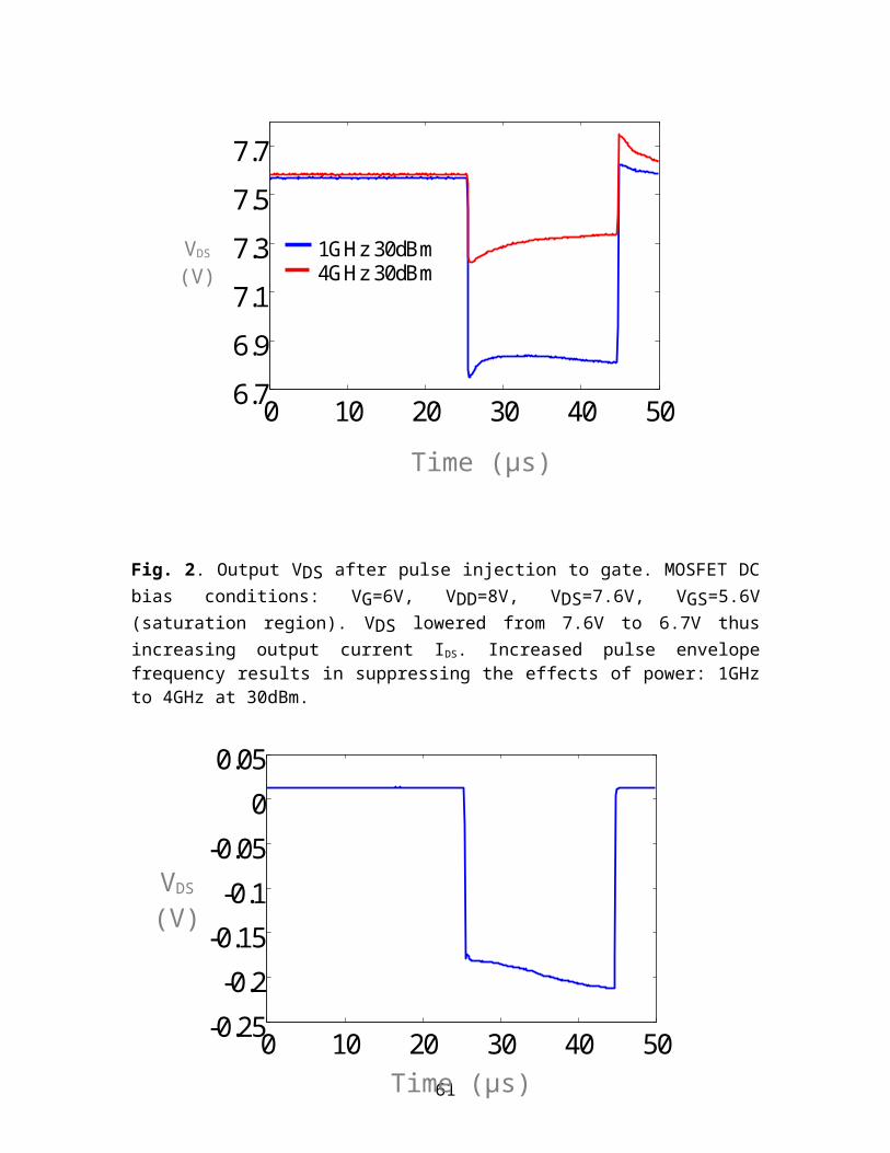
APPENDIX
Boise State University MURI Update: (September 2003-present)
Summary:1. Continue to use Schottky diodes to measure microwave power in CMOS integrated
circuits.1. Design Simple Integrate Circuit Building Blocks (SICBBs) for test
1. Designed and laid out test structures (four chips) consisting of an inverter, diff-amp, and amplifier.
2. Submitted the chips for fabrication in a 500 nm CMOS process.3. Updated software in the microwave probe station for making measurements
when the chips are tested this fall2. SICBBs Reliability Update:
1. MOSFETs: Gate Oxide Thickness = 3.2 nm1. Exploring the effects of soft breakdown (SBD) on MOSFET and inverter
circuit operation.2. Developing charge pumping techniques to investigate trap density and energy
with respect to specific oxide degradation mechanisms.3. Initiated 2nd the SICBB study using transmission gate (TG) circuit to compare
DC and time domain characteristics to the inverter circuit.2. MOSCAPs and MOSFETs: Gate Oxide Thickness = 2.0 nm
4. Obtained experimental data from MOSCAPs in which we observed multiple oxide breakdown (BD) regimes (different than observed regimes in 3.2nm oxides). This work is used to predict BD in MOSFETs with equal oxide thickness.
5. Investigating the breakdown regimes in both nMOSFET and pMOSFET devices, in conjunction, analyzing the difference in device behavior between accumulation and inversion modes.
6. Studying the effects of SBD on MOSFET and inverter circuit operation. This work extends/parallels the ongoing research for 3.2 nm oxides in order to investigate oxide thickness scaling.
3. Equipment Update:New equipment/software purchases allow for the detection of the first instance of very faint or subtle breakdown in two similar systems:
7. Keithley 4200 Semiconductor Characterization System upgrades with new software, processor upgrade, and 2 Preamps upgrading the current sensitivity level.
8. Keithley 707A Switch Matrix containing (2) 7174A 8x12 low leakage matrix cards.
9. Metrics IC/V Characterization software used with the Agilent 4156C Semiconductor Parameter Analyzer and the Agilent E5250A Switch Matrix.
10. Agilent 7484A LCR Meter
61

11. Agilent Infiniium 54832D Oscilloscope 1Ghz12. Agilent Equipment Rack System
4. Publication Update:3. Published and/or Presented:
13. Cheek, Betsy J., Stutzke, Nate, Santosh Kumar, R. Jacob Baker, Amy J. Moll and William B. Knowlton, Investigation of Circuit-Level Oxide Degradation and its Effect on CMOS Inverter Operation Performance and MOSFET Characteristics, in proceedings of the 2004 IEEE International Reliability Physics Symposium (April, 25-29, 2004) pp. 110-116.
14. M. L. Ogas, R. G. Southwick III, B. J. Cheek, C. E. Lawrence, S. Kumar, A. Haggag, R. J. Baker, W. B. Knowlton, Multiple Waveform Pulse Voltage Stress (MWPVS) Technique for Modeling Noise in Ultra Thin Oxides, poster presentation at 2004 IEEE Workshop on Microelectronics and Electron Devices (April 16, 2004).
15. Dorian Kiri, Michael L. Ogas, Ouahid Salhi, Richard G. Southwick III, Gennadi Bersuker, Betsy J. Cheek, William B. Knowlton, Investigation of Ultra Thin Gate OxideReliability in MOS Devices and Simple ICs, poster presentation at 2004 IEEE Workshop on Microelectronics and Electron Devices (April 16, 2004).
4. Accepted and/or Submitted:16. M. L. Ogas, R. G. Southwick III, B. J. Cheek, R. J. Baker, G. Bersuker, W. B.
Knowlton, Survey of Soft Breakdown (SBD) in 2.0 nm Gate Oxides in MOS Devices and Inverter Circuits, accepted for oral presentation at 2004 IEEE International Integrated Reliability Workshop (Oct, 20-23, 2004).
17. Betsy J. Cheek, Santosh Kumar, R. Jacob Baker, Amy J. Moll and William B. Knowlton, Examination of Transistor-Level Current Limited Hard Breakdown (LHBD) and Its Effect on CMOS Inverter Circuit Operation, submitted for publication in IEEE Transactions on Electron Devices.
5. CollaborationInternational SEMATECH, Austin, Texas – Dr. Gennadi Bersuker
Investigate the reliability of 2nm gate oxide devices and circuits.
62

Example work performed under this grant
INVESTIGATION OF CIRCUIT-LEVEL OXIDE DEGRADATION AND ITS EFFECT ON CMOS CIRCUIT OPERATION
PURPOSE
Circuit-level oxide degradation effects on CMOS inverter circuit operation and individual MOSFET behavior is investigated. Individual PMOSFET and NMOSFET devices are assembled off-wafer in the inverter configuration through a switch matrix. A range of gate oxide degradation mechanisms are induced by applying a ramped voltage stress (RVS) of various magnitudes to the input of the inverter. A novel circuit model is used to simulate the voltage transfer curves (VTCs) of degraded inverters. At the transistor level, increased gate leakage currents of nearly eight orders of magnitude are observed, in addition to severely reduced on-currents (> 50 percent reduction), and large threshold voltage (Vth) shifts (> 100 mV). At the circuit-level, stress of either polarity results in inverter performance degradation. For the DC characteristics, oxide degradation attributed to limited hard breakdown (LHBD) in the NMOSFET and hard breakdown (HBD) in the PMOSFET, results in decreased output voltage swing (> 260 mV). Under the same conditions, inverter degradation in the voltage-time (V-t) domain exposes much larger changes in performance. For instance, significant increase in the rise time results in the output voltage being pulled up to only 660 mV (VDD = 1.8 V) before switching low. From a circuit reliability viewpoint, it may be possible for subsequent circuit stages to compensate for a few degraded devices, but in high-speed circuits, increased rise/fall and delay times may cause timing issues. Furthermore, increased gate or off-state leakage currents can potentially load previous circuit stages or result in increased power consumption. [Keywords: Circuit model, circuit reliability, CMOS, dielectric breakdown, gate oxide reliability, inverter degradation, MOSFEET degradation.]
INTRODUCTION
The continued importance of gate oxide breakdown and reliability may be a limiting factor in the future scaling of high performance CMOS integrated circuits [1, 2]. Many studies have been conducted on gate dielectric breakdown of individual MOS capacitors and an increasing number on MOSFETs (for an overview, see [3]). Only a limited number of investigations consider the effects of circuit-level stress on circuit performance and reliability [4-8]. Large integrated circuits with a large number of transistors have been the focus of many of these studies. In complex circuits, such as digital and RF, it has been demonstrated that hard breakdown (HBD) in multiple MOSFETS does not cause total circuit failure, but these circuits remain functional [7, 9]. And although it has been reported that subsequent circuit stages may be capable of compensating for a few degraded devices [7], increased rise/fall and delay times may result in potential timing issues in high-speed circuits. Furthermore, in complex integrated circuits, it may only be possible to examine the effects of stress on the circuit as a whole. Potential circuit reliability issues may be better understood by directly measuring the amount of gate oxide degradation in individual MOSFETs that have been
stressed within a circuit, which is the focus of this study. This is accomplished by stressing simple integrated circuit building blocks (SICBBs) such as transmission gates, current mirrors, and inverters, which are the focus of this study. Therefore, using simple circuits comprised of MOS devices that can be isolated from the circuit and characterized directly, can provide a foundation for understanding gate oxide degradation effects on large-scale circuits
EXPERIMENTAL
PMOSFET and NMOSFET transistors fabricated in a 0.16-m/1.8-V CMOS technology with gate oxide thickness of 3.2 nm and gate dimensions of 25μm x 25μm are connected in an inverter configuration (Fig. 1) off-wafer via an Agilent E5250A low leakage switch matrix. Characterization and stress tests are performed with an Agilent 4156C Precision Semiconductor Parameter Analyzer, an Agilent 41501B pulse generator, an Agilent Infinium oscilloscope, and a probe station equipped with eight Cascade Microtech DCM positioners enclosed in a Faraday cage.
63

VOUT 0 V VDD VIN
The flow chart in Fig. 2 simplifies the following procedures used during circuit-level stress experiments. The inverter circuits are investigated under both positive and negative stress conditions. A ramped voltage stress (RVS) is applied from input to output with the VDD and GND terminals floating [10], as shown in Fig. 3. The maximum value of the ramped voltage is varied to induce multiple degrees of gate oxide degradation, which ranged from 0 to +/- 8 V, 0 to +/- 10 V, 0 to +/- 12 V, and 0 to +/- 14 V. The former two RVS ranges have been shown to induce current limited hard breakdown (LHBD) [11, 12] while the latter two RVS ranges were used in an attempt to reproduce the data of [13]. A series of pre- and post-stress tests are conducted on the inverter to examine performance changes in the inverter voltage transfer characteristics (VTCs) and voltage-time (V-t) domain characteristics. For inverter performance measurements, the input voltage (VIN), power supply voltage (VDD), test frequency, and duty cycle, were 1.8 V, 2.5 kHz, and 50 percent, respectively. In addition, all inverter leakage currents are monitored, pre- and post-stress, by connecting VOUT, VDD, and GND nodes to 0 V. See [14] for an overview of inverter circuit operation and other parameters discussed in this study.
64
Measure Fresh response:MOSFET (IG-VG, ID-VD, ID-VG)
Inverter (VTC, V-t)
New devices or circuit?
Apply Stress to input of inverter
Measure Post-stress response:MOSFET (IG-VG, ID-VD, ID-VG)
Inverter (VTC, V-t)
Start testsequence
End all tests
yn
FIGURE 2. FLOW CHART.
FIGURE 1. WAFER LEVEL INVERTER CONFIGURATION FOR CIRCUIT-LEVEL STRESS EXPERIMENTS.

The type and amount of degradation observed for each MOSFET, as a result of circuit-level stress, are identified by comparing pre- and post-stress gate leakage current versus gate voltage (IG-VG) measurements. IG-VG measurements are taken with the drain (D), source (S), and bulk (B) terminals at ground potential. The DC parameters selected for examining the effects of degradation on individual MOSFET characteristics before and after circuit-level stress are maximum drain current (ID,MAX), on-current (IOn), off-current (IOff), subthreshold slope (S). The absolute value of the data is plotted where appropriate.
PROPOSED CIRCUIT MODEL
Various circuit models for stressed inverters have been proposed [13, 15]. It was reported [15] that the percolation path at the breakdown spot is primarily composed of phosphorus from the n+-polysilicon gate. This results in the formation of an ohmic contact to the n+ source/drain regions of the NMOSFET. It has been suggested that an ohmic model does not provide a good fit for experimental data of inverters [13] if the degradation mechanism observed is not comparable to hard breakdown (HBD). Furthermore, the diode effect for both transistors may be explained if the percolation path, or at least the contact to drain regions, is intrinsic silicon.
To simulate the operation of degraded inverter VTCs, the circuit model shown in the inset of Fig. 4(a) was used. The model is similar to that in [15]. However, rather than the PMOSFET, a resistor-diode pair is introduced to simulate gate-to-drain breakdown in the NMOSFET and the PMOSFET. The resistors from MOSFET gates (VIN) to sources (VDD, GND) are altered to accommodate the statistical distribution of the post-breakdown resistance of the percolation path. MOSFET threshold voltage shifts are included in the model to provide a closer fit to the experimental results. The Shockley diode equation [16] is given by:
(1) where the parameters are defined as saturation current (IS), diode voltage (VD), emission coefficient (N), and thermal voltage (Vt). Adjusting the variable, N, alters the bias voltage at which the diodes begin conducting.
EXPERIMENTAL RESULTS
Inverter Performance
Experimental and simulated VTCs for inverters stressed in circuit-level configuration are shown in Fig. 4(a) and (b).
65
FIGURE 3. INVERTER SCHEMATIC. VOLTAGE SOURCE INDICATES STRESS WAS INDUCED FROM VIN TO VOUT.
- + VIN
GND
VOUT
VDD

Solid lines represent experimental data and symbols indicate simulated VTCs. In general, as the magnitude of the positive stress increases [Fig. 4(a)], VOH decreases and VOL increases, resulting in decreased inverter output swing.
It is observed from Fig.4(a) that when the devices have suffered the highest degree of LHBD (NMOSFET) and HBD (PMOSFET), a decrease in VOH by as much as 20 mV is observed. The change in VOL is even greater showing an increase of as much as 240 mV. In general, the changes in VOL occur at lower stress voltages than those in VOH. VSP
initially increases or shifts right with increasing stress magnitude. At the highest stress voltages, VSP decreases and is similar to that of the fresh inverter.
VTC results for negative circuit-level stress [Fig. 4(b)] are similar, but have slightly different trends. Compared to the positive stress case, VOH and VOL tend to decrease with increasingly negative stress. The change in VOH is typically larger for negative stress than for positive stress, while VOL is typically highest at low stress voltages, and then decreases with increasing stress voltage. VSP tends to shift left and initially decreases with increasing stress magnitude, similar to the response observed in VOL.
From the VTCs alone, it appears that the inverter performance has not been severely degraded at lower stress voltages. However, examining the time-domain behavior reveals otherwise. Shown in Fig. 5 are the time-domain responses, to a 2.5 kHz square wave input, of inverters that have been stressed with a (a) positive RVS and (b) negative RVS.
66
FIGURE 4. INVERTER VTCS FOLLOWING (A) POSITIVE AND (B) NEGATIVE VOLTAGE
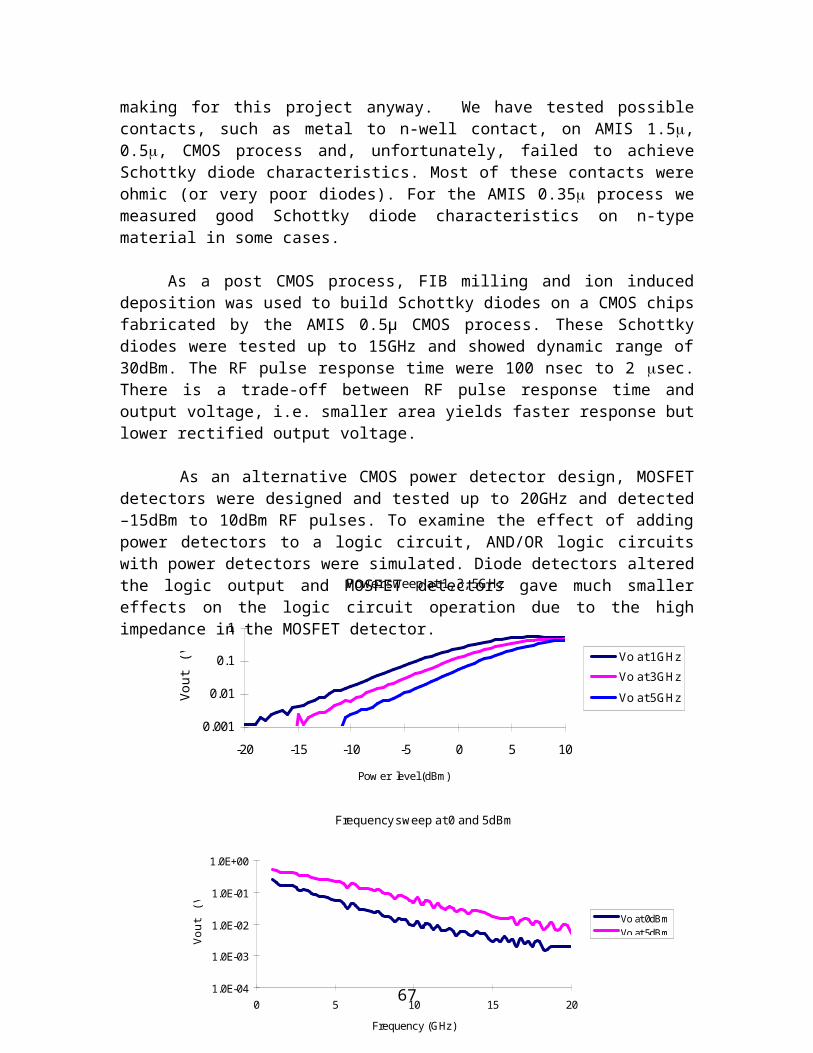
Similar to the VTC operation, the inverter V-t domain describes two areas of interest, which are designated as region and II. Region is defined as the rising signal or PMOSFET pull-up portion. Region corresponds with the falling signal or NMOSFET pull-down portion.
In general, after positive/negative stress, it is observed that as the stress magnitude is increased the inverter voltage output swing in the time domain is significantly decreased. It is interesting to note that the trends in region and region follow those trends observed in Fig. 4 for VOH and VOL, respectively, which are attributed to the NMOSFET being degraded to LHBD and the PMOSFET suffering HBD. However, under the same conditions, region I of (a) and (b) shows that VOut,MAX has decreased from 1.8 V fresh to 660 mV/440 mV, respectively. In comparison, VOH decreased from 1.8 V fresh to 1.78 V post-stress. Conversely, for region of (a) and (b), the voltage magnitude of VOut,MIN is very similar to that observed in VOL from the transfer characteristics.
Unlikeregion I, which shows that as the stress magnitude is increased (positive or negative) VOut,MAX is significantly decreased, region II shows an opposite behavior for each stress polarity. For instance, in the positive stress case [Fig. 5(a)], VOut,MIN increases with increasing stress magnitude and reaches a maximum of 248 mV (ideal = 0 V). Alternatively, for negative stress [Fig. 5(b)] VOut,MIN increases with decreased stress magnitude to a maximum of 196 mV.
Inverter input leakage currents following (a) negative and (b) positive voltage stress are shown in Fig. 6.
67
FIGURE 5. INVERTER V-T RESPONSE AFTER (A) POSITIVE AND (B) NEGATIVE STRESS. VIN DEFINES THE DIGITAL INPUT SIGNAL, FRESH AND VARIOUS
STRESS VOLTAGES REPRESENT THE DIGITAL OUTPUT SIGNAL.

Various degrees of inverter degradation are observed for both stress polarities. Input leakage current is typically highest at -1.8 V for both cases. Furthermore, leakage currents for negative stress are generally higher at operating conditions (VG = 1.8 V) where a difference of approximately 20 A or more is observed, relative to positive stress of equal magnitude.
MOSFET Characteristics
Gate leakage current results following negative and positive stress for the NMOSFET and PMOSFET are shown in Fig 7. In general, as stress magnitude increases, gate leakage current of both the NMOSFET and PMOSFET increases, as would be expected. The relationship between the proposed breakdown mechanism attributed to the leakage current response is not always easily identified, as indicated by the (?) in Fig.7(c) and (d). Typically the NMOSFET suffers limited hard breakdown (LHBD) [11, 12] for all stress voltages, while the PMOSFET is more likely to breakdown to a greater extent at higher stress voltages. In addition, the leakage current for negative stress [(a)/(c)] increases over one order of magnitude at +/- 1.8V, while positive stress [(b)/(d)] increases over two orders of magnitude. Comparison of Fig. 7(b) and (d) reveals that under multiple (+) V stress conditions, the NMOSFET suffers from LHBD while the PMOSFET has undergone HBD. This behavior is present for negative circuit-level stress as well [Fig. 7(a) and (c)]. Various breakdown modes have been induced in the PMOSFET, as indicated by the labels in Fig. 7(d), but similar modes are observed for each device after both positive and negative stress. As the stress magnitude increases, a large range of LHBD is observed, which at times is followed by HBD.
One of the more interesting observations, which is present at varying degrees for both devices under numerous stress conditions, is the difference in initial leakage current magnitude and characteristic between the low (< 0.9 V) and the high (> 0.9 V) voltage regimes. The first trend may be described more clearly by comparing Fig. 7(c) and (d). For the PMOSFET under (-) 8 V stress, the leakage current measured at VG = 0 V is two orders of magnitude higher than
68
FIGURE 6. FRESH AND POST-STRESS INVERTER INPUT LEAKAGE CURRENTS MONITORED FOR (A) NEGATIVE AND (B) POSITIVE STRESS EXPERIMENTS.

the Fresh characteristic, while for (+) 8 V stress the leakage current at VG = 0 V is consistent with the Fresh measurement.
The second observation is made relative to the characteristic or shape differences between the low and high voltage regimes. In this case, Fig. 7(b) easily identifies the two regions of interest. For each stress voltage in the range VG > 0.9 V, their relative shape’s are similar and the leakage current begins to level off as it approaches 1.8 V. Conversely, in the low voltage regime, the current may change slopes up to three times before entering the high voltage region, where the current increases more steadily. This behavior appears to be independent of the operating mode, as it present for both accumulation and inversion. However, this behavior is more pronounced in inversion mode, for both the NMOSFET and PMOSFET devices.
The subthreshold characteristics for the NMOSFET and PMOSFET devices following +/- V stress are shown in Fig. 8. The oxide degradation mechanism for each device was determined to be LHBD. It is observed that the subthreshold slope has increased by as much as 19 mV/decade in the NMOSFET and 8 mV/decade in the PMOSFET. For (-) V stress, the change in on-current (IOn) is observed to be higher for both the NMOSFET and PMOSFET. Conversely, the change in off-current (IOff) for the PMOSFET is greater after (+) V stress when compared to the NMOSFET. Fig. 9 shows the ID-VD characteristics for each device after various degrees of (a)/(b) positive and (c)/(d) negative stress. Curves
69

70
FIGURE 7. POST-STRESS IG-VG LEAKAGE CURRENT PLOTS FOR (A) NMOS (- V), (B) NMOS (+ V), (C) PMOS (- V), AND (D) PMOS (+ V) STRESS.
FIGURE 8. COMPARSION OF THE LOG ID-VG CHARACTERSTICS FOR NMOS AND PMOS DEVCES.

for |VGate| of 1.8 V are plotted, but the behavior is similar for lower gate voltages. Generally, as stress magnitude increases, a substantial decrease in ID,MAX is observed. However, from Fig. 9 it is apparent that different trends are observed for positive and negative stress. It is interesting to note that Fig. 9(a) and (c) are the result of LHBD in an NMOSFET, while Fig. 9(b) and (d) are the result of both LHBD and HBD in the PMOSFET.
In order to evaluate these results, each plot identifies two areas of interest are identified in each plot. A1 and A2 are designated as the linear and saturation regions, respectively [16]. The relationship between the drain-to-source voltage (VDS), gate-to-source voltage (VGS), and MOSFET threshold voltage (Vth) are given for each area in expressions (2) and (3).
VDS ≤ VGS –Vth , for A1 (2)
and
VDS ≥ VGS –Vth, for A2. (3)
Additionally, region A1 requires that for the MOSFET to be turned “on”, VGS > Vth, otherwise VGS < Vth and the device is “off”. It is observed from Fig. 9(a) and (b) that regions A1 and A2 follow a similar trend after positive stress of either the NMOSFET or the PMOSFET. Experimental results show that as the magnitude of the stress increases, ID,MAX
decreases. However, regions A1 and A2 of Fig. 9(c) and (d) do not follow the same trend. Typically for negative stress, region A1 is similar to the positive stress results, yet the negative results for (c) region A2, indicate that at lower stress magnitudes ID,MAX for the NMOSFET decreases significantly compared to higher stress voltages. A similar trend for ID,MAX is observed for the PMOSFET(d) for stress resulting from HBD.
For a discussion concerning the effects of circuit-level stress on the MOSFET parameters transconductance (gm) and threshold voltage (Vth) refer to [14].
71

72
FIGURE 9. ID-VD RESULTS INDICATING ID,MAX DEGRADATION FOR (A) NMOS (+), (B) PMOS (+), (C) NMOS (-), AND (D) PMOS (-)
STRESS.

DISCUSSION
Inverter Performance
Both stress polarities induced LHBD and/or HBD (Fig. 7) which resulted in reduced output swing of the inverter VTC (Fig. 4), comparable to observations in [5]. Shifts in inverter VSP are also observed when the inverter is stressed (Fig. 4). As reported in [4], this could be due to interface state generation or charge trapping in the oxide [17], or possibly a combination of both. In general, as the stress magnitude is increased, VSP increases. However, a clear correlation between stress magnitude and the amount of VSP shift is not always apparent.
A link between VTC performance and region II of the V-t response can be seen by comparing VOL (Fig. 4) and VOut,MIN (Fig. 5). The post-stress V-t results following positive and negative circuit-level stress, indicate that VOut,MIN is consistent with VOL for both stress polarities. This may be explained by the difference in response of the NMOSFET to the polarity of the stress in the saturation region (A2) of the ID-VD characteristics [Fig. 9(c)]. For increasing negative polarity, a general increase in ID is observed in the A2 region which should manifest a decrease in VOL [Fig. 4(b)] and VOut,MIN [Fig. 5(b)]. However, the inverse relation is observed. The opposite occurs for positive stress polarity as seen in Fig. 4(a) and 5(a). The opposing circuit responses to changes in polarity may be due to the leakage currents at the various terminals of the inverter. These behaviors are currently being examined.
Unlike VOut,MIN, the magnitude of the response for VOut,MAX does not match that of the VTC (Fig. 4 and 5). One particular discrepancy is observed with respect to the rise time. Several factors may attribute to the rise-time increase, such as a decrease in the effective carrier mobility of the PMOSFET due to interface states created during stressing [17], the large area of the devices, or the inverter device ratio being 1:1 (PMOS:NMOS), where a more ideal case would be a ratio of at least 2:1 [16]. Moreover, increased charging time for parasitic capacitances, due to increased leakage currents, may also limit the rise-time. However, if the test frequency is decreased significantly, the final VOut,MAX
values approach those of the VTCs.
Perhaps the most important or viable observation is that the time-domain exhibits significant degradation compared to the VTCs under equal amounts of stress. This substantial difference prompts the question, which characteristic would be better suited for evaluating reliability limits for inverters? This study suggests that the time-domain be investigated when examining the effects of oxide degradation in the inverter circuit. When both devices behave more resistively (Fig. 9), the time domain behavior of the inverter will change. Furthermore, if the resistance of the inverter increases, the delay and transition times (tr and tf) [14] of the inverter will increase. The relationships between delay and resistance are given by [16]:
(4) and
(5)
where tplh and tphl are defined as the propagation delay from low-to-high and from high-to-low, Rp and Rn are defined as the effective resistance (resistance between drain and source) of the PMOSFET and NMOSFET, and Ctot is the sum of all capacitive components on the output of the inverter. From (4) and (5) above, it may also be understood that if the loading from the measurement system is significant then the selection of the width and length of the device is not a factor, as it will just scale the transition or delay times for both fresh and degraded devices.
MOSFET Characteristics
Changes in MOSFET parameters such as ID,MAX, gm, and the subthreshold characteristics were observed following circuit-level stressing. When the gate oxide suffers dielectric breakdown under circuit-level stress, gate control over the channel may be severely reduced (Fig. 9). This can alter the polarity of the current in the linear region (A1) thus inhibiting channel inversion. The differences observed in regions A1 and A2, particularly for negative stress, suggest that changes in the threshold voltage are less for lower stress voltages, which results in the degraded device turning on more quickly (steeper slope), thus saturating at a lower current level. Additionally, off-state currents often increase (Fig. 8) which can result in increased power consumption [16].
73

A range of oxide degradation occurs following circuit-level stress, such as LHBD and HBD. Of particular interest is the evidence that MOSFETs can independently experience different degradation mechanisms while in the inverter configuration [Fig. 7(a) and (c)]. For either polarity, the device suffering a higher degree of oxide degradation (Fig. 8 and 9) may be the dominant cause of circuit failure. Further, MOSFET inversion mode operation (Fig. 9) seems to be more heavily influenced by negative voltage stress, supported by leakage current data in Fig. 7. This suggests that the PMOSFET is influenced more by inversion stress and the NMOSFET by accumulation mode stress.
Comparing the leakage currents of degraded MOSFETs (Fig. 7) to those of degraded inverters (Fig. 6), similarities between the two are evident. In addition, the trends observed for the low and high voltage regimes are observed in both cases. However, there are some differences that are currently under investigation, which may be attributed to current leakage at the drain, source, and bulk nodes of the devices.
Circuit Model
VTCs of positive and negative stressed inverters (Fig. 4) are fit well by varying a few parameters contained in the model. The development of this model came about after preliminary examination of the individual transistor leakage current components. The data suggests that the drain current is usually lowest and diode-like, whereas the substrate and/or source currents are usually highest and nearly linear (i.e. ohmic). However, these results may vary depending on the MOSFET operation mode being investigated. Consequently, these findings may be a result of the manner in which the inverter is stressed. The ideas presented here are only preliminary and are currently being extended.
It has been reported that in certain digital applications, the gate-to-source leakage current may generate a worst case scenario [6]. For this study, further examination of the leakage current components suggests that gate-to-substrate leakage currents may dominate the total leakage current. In addition to the preliminary analysis of the leakage currents, Spice simulations revealed that only gate-to-drain breakdowns seem to affect the inverter VTCs. Conversely, inverter time-domain performance was shown to be severely degraded when little to no gate-to-drain breakdown was observed (Fig. 5). These discrepancies can potentially be addressed by simulating the voltage-time domain behavior with the model presented in this study, or perhaps by incorporating other circuit elements. To perform this task, additional analysis of all MOSFET leakage currents is required and is currently being investigated.
CONCLUSION
Circuit-level stress effects on circuit operation and individual transistors were investigated. Circuit stress of either polarity, on the transistor-level, results in increased gate leakage current, decreased ID,MAX, decreased gm and increased Vth [14] for the NMOSFET and the PMOSFET. More compelling is the evidence that the NMOSFET and PMOSFET can suffer dissimilar oxide degradation mechanisms while in the inverter configuration.
Simulations of degraded inverter VTCs were accomplished using a new circuit model. Decreased inverter voltage output swing was observed in both the transfer characteristics and the time domain. However, more significant changes were observed with respect to the inverter rise and fall times. Hence, VTC measurements may show negligible inverter degradation; yet, V-t behavior of the inverter may be severely degraded. Consequently, the V-t data, presented for the first time, introduces a new characteristic for digital circuit reliability. Several published reports call for more suitable circuit reliability criterion [6, 7, 10].
In larger circuits, stages subsequent to a degraded SICBB may be able to compensate for adverse SICBB operation [7], however, increased rise/fall times and delays could lead to timing in high speed circuits. Although VTC degradation may be limited, large leakage and off-state currents can be present potentially inducing loading of previous circuit stages and increased power consumption [16]. It seems apparent that further investigation of circuit reliability is prudent.
REFERENCES
[1] J. H. Stathis and D. J. DiMaria, "Reliability projection for Ultra-thin oxides at low voltage," IEDM'98, pp. 167-169, 1998.
[2] H. Iwai and H. S. Momose, "Ultra-thin gate oxides-Performance and Reliability," IEDM Proc., pp. 163-166, 1998.
[3] D. J. Dumin, "Oxide wearout, breakdown, and reliability," International Journal of High Speed Electronics and Systems, vol. 11, pp. 617-718, 2001.
[4] R. Rodriguez, J. H. Stathis, and B. P. Linder, "Modeling and experimental verification of the effect of gate oxide breakdown on CMOS inverters," presented at IRPS Proc., pp 11-16, 2003.
[5] J. H. Stathis, R. Rodriguez, and B. P. Linder, "Circuit Implications of gate oxide breakdown," WoDim, 2002.
74
[6] R. Rodriguez, J. H. Stathis, B. P. Linder, S. Kowalczyk, C. T. Chuang, R. V. Joshi, G. Northrop, K. Bernstein, A. J. Bhanvnagarwala, and S. Lombardo, "The impact of gate-oxide breakdown on SRAM stability," IEEE Transactions on Device Letters, vol. 23, pp. 559-561, 2002.
[7] B. Kaczer, R. Degraeve, M. Rasras, K. Van de Mieroop, P. J. Roussel, and G. Groeseneken, "Impact of MOSFET gate oxide breakdown on digital circuit operation and reliability," IEEE Transactions on Electron Devices, vol. 49, pp. 500-506, 2002.
[8] B. Kaczer, R. Degraeve, G. Groeseneken, M. Rasras, S. Kubicek, E. Vandamme, and G. Badnes, "Impact of MOSFET oxide breakdown on digital circuit operation and reliability," presented at IEDM Tech. Dig., 2000.
[9] H. Yang, J. S. Yuan, and E. Xioa, "Effect of gate oxide breakdown on RF device and circuit performance," IRPS, 2003.
[10] J. H. Stathis, R. Rodriguez, and B. P. Linder, "Circuit implications of gate oxide breakdown," Microelectronics Reliability, vol. 43, pp. 1193-1197, 2003.
[11] B. P. Linder, J. H. Stathis, R. A. Wachnik, E. Wu, A. R. Cohen, and A. Vayshenker, "Gate oxide breakdown under current limited constant voltage stress," 2000 Symposium on VLSI Technology Digest of Technical Papers, pp. 214-215, 2000.
[12] W. B. Knowlton, S. Kumar, T. Caldwell, J. Gomez, and B. Cheek, "On the nature of ultrathin gate oxide degradation during pulse stressing of nMOSCAPs in accumulation," presented at Proceedings of the International Integrated Reliability Workshop, pp. 87-88, 2001.
[13] R. Rodriguez, J. H. Stathis, and B. P. Linder, "A model for gate-oxide breakdown in CMOS inverters," IEEE Electron Device Letters, vol. 24, pp. 114-116, 2003.
[14] N. Stutzke, B. J. Cheek, S. Kumar, R. J. Baker, A. J. Moll, and W. B. Knowlton, "Effects of Circuit-Level Stress on Inverter Performance and MOSFET Characteristics," in proceedings 2003 IEEE International Integrated Reliability Workshop, 2003, pp. 71-79.
[15] T.-S. Yeoh and S.-J. Hu, "Influence of MOS transistor gate oxide breakdown on circuit performance," presented at ICSE'98, Bangi, Malaysia, pp. 59-63, 1998.
[16] R. J. Baker, H. W. Li, and D. E. Boyce, "CMOS: Circuit design, layout, and simulation," IEEE Press, 1998, pp. 201-229.
[17] Q. Li, J. Zhang, W. Li, J. S. Yuan, Y. Chen, and A. S. Oates, "RF circuit performance degradation due to soft breakdown and hot-carrier effect in deep submicrometer CMOS technology," IEEE Transactions on Microwave Theory and Techniques, vol. 49, pp. 1546-1551, 2001.
75