analysis of material modifications induced during laser damage in sio2 thin films
TRANSCRIPT

www.elsevier.com/locate/optcom
Optics Communications 272 (2007) 221–226
Analysis of material modifications induced during laserdamage in SiO2 thin films
L. Gallais *, J. Capoulade, F. Wagner, J.Y. Natoli, M. Commandre
Institut Fresnel (UMR CNRS), Ecole Generaliste d’Ingenieurs de Marseille, Universite de Provence, Universite Paul Cezanne,
Domaine Universitaire de St Jerome, 13397 Marseille Cedex 20, France
Received 21 August 2006; received in revised form 13 November 2006; accepted 15 November 2006
Abstract
The damage mechanisms in silica thin films exposed to high fluence 1064 nm nano-second laser pulses are investigated. The thin filmsunder study are made with different techniques (evaporation and sputtering, with and without ion assistance) and the results are com-pared. The material morphological, optical and structural modifications are locally analyzed with optical microscopy and profilometry,photoluminescence and absorption microscopies. These observations are made for fluences near and above the laser damage threshold,and also in the case of multiple pulse irradiations. An increase in absorption in and around the damages is observed, as well as the gen-eration of different defects that we spatially resolve with absorption and luminescence mappings.� 2006 Elsevier B.V. All rights reserved.
Keywords: Laser induced damage; Optical coatings; Silica
1. Introduction
Laser induced damage in optical materials is a key issuefor high power laser applications, and a significant numberof studies have been published since the advent of lasers. Itis widely acknowledged that the damage initiation in thenano-second regime on the surface of wide band-gap mate-rials such as silica, is linked to the presence of nano tomicrometer sized defects. These nanometric laser damageprecursors may originate from the manufacturing processes(cleaning, polishing, coating) [1–3]. The study of the laserdamage initiation mechanisms is difficult, mainly becausethe identification of nanometric laser damage initiatorswith low density on silica surfaces is still an issue. To over-come this problem, one solution is to intentionally intro-duce laser damage initiators and study their behaviour
0030-4018/$ - see front matter � 2006 Elsevier B.V. All rights reserved.
doi:10.1016/j.optcom.2006.11.025
* Corresponding author. Tel.: +33 4 91 28 80 72; fax: +33 4 92 28 80 67.E-mail address: [email protected] (L. Gallais).URL: www.fresnel.fr (L. Gallais).
under laser irradiation. Progress has recently been madein the understanding of the laser damage process by study-ing artificial defects of known size and composition,embedded in silica thin films [4,5]. However the mecha-nisms could be very different on ‘real’ samples. Due tothe low surface density of the damage precursors, investiga-tions on real samples are usually based on the analysis ofalready damaged sites [6–9].
For this work we define the ‘Damage Threshold’ of thesample as the lowest fluence at which we observe mechan-ical damage of the sample by Normarsky microscopy. Wedescribe here observations of a very early state of laserinduced damage, that often is not detected. Using opticalprofilometry, absorption mappings and luminescence map-pings, we also detected laser induced material modifica-tions on ‘undamaged’ sites (according to the definitionabove). We will summarize these modifications by the word‘pre-damage’. The study has been carried out on bare fusedsilica substrates and on silica coatings deposited on thesesubstrates.
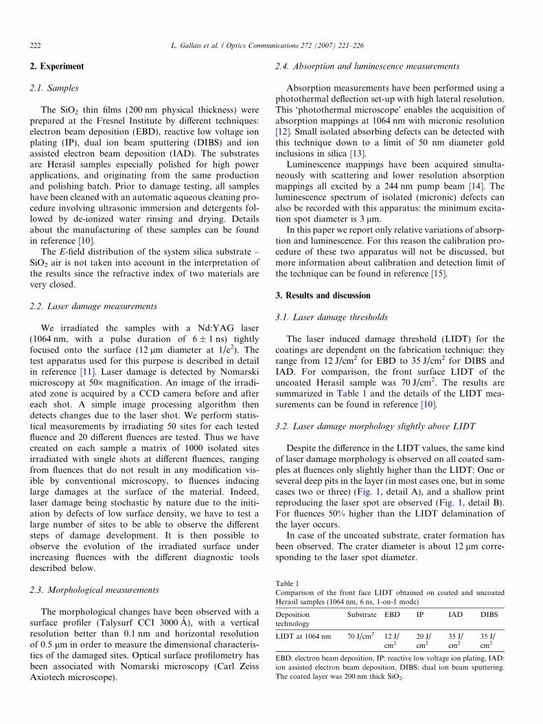
Table 1Comparison of the front face LIDT obtained on coated and uncoatedHerasil samples (1064 nm, 6 ns, 1-on-1 mode)
Depositiontechnology
Substrate EBD IP IAD DIBS
LIDT at 1064 nm 70 J/cm2 12 J/cm2
20 J/cm2
35 J/cm2
35 J/cm2
EBD: electron beam deposition, IP: reactive low voltage ion plating, IAD:ion assisted electron beam deposition, DIBS: dual ion beam sputtering.The coated layer was 200 nm thick SiO2.
222 L. Gallais et al. / Optics Communications 272 (2007) 221–226
2. Experiment
2.1. Samples
The SiO2 thin films (200 nm physical thickness) wereprepared at the Fresnel Institute by different techniques:electron beam deposition (EBD), reactive low voltage ionplating (IP), dual ion beam sputtering (DIBS) and ionassisted electron beam deposition (IAD). The substratesare Herasil samples especially polished for high powerapplications, and originating from the same productionand polishing batch. Prior to damage testing, all sampleshave been cleaned with an automatic aqueous cleaning pro-cedure involving ultrasonic immersion and detergents fol-lowed by de-ionized water rinsing and drying. Detailsabout the manufacturing of these samples can be foundin reference [10].
The E-field distribution of the system silica substrate –SiO2 air is not taken into account in the interpretation ofthe results since the refractive index of two materials arevery closed.
2.2. Laser damage measurements
We irradiated the samples with a Nd:YAG laser(1064 nm, with a pulse duration of 6 ± 1 ns) tightlyfocused onto the surface (12 lm diameter at 1/e2). Thetest apparatus used for this purpose is described in detailin reference [11]. Laser damage is detected by Nomarskimicroscopy at 50· magnification. An image of the irradi-ated zone is acquired by a CCD camera before and aftereach shot. A simple image processing algorithm thendetects changes due to the laser shot. We perform statis-tical measurements by irradiating 50 sites for each testedfluence and 20 different fluences are tested. Thus we havecreated on each sample a matrix of 1000 isolated sitesirradiated with single shots at different fluences, rangingfrom fluences that do not result in any modification vis-ible by conventional microscopy, to fluences inducinglarge damages at the surface of the material. Indeed,laser damage being stochastic by nature due to the initi-ation by defects of low surface density, we have to test alarge number of sites to be able to observe the differentsteps of damage development. It is then possible toobserve the evolution of the irradiated surface underincreasing fluences with the different diagnostic toolsdescribed below.
2.3. Morphological measurements
The morphological changes have been observed with asurface profiler (Talysurf CCI 3000 A), with a verticalresolution better than 0.1 nm and horizontal resolutionof 0.5 lm in order to measure the dimensional characteris-tics of the damaged sites. Optical surface profilometry hasbeen associated with Nomarski microscopy (Carl ZeissAxiotech microscope).
2.4. Absorption and luminescence measurements
Absorption measurements have been performed using aphotothermal deflection set-up with high lateral resolution.This ‘photothermal microscope’ enables the acquisition ofabsorption mappings at 1064 nm with micronic resolution[12]. Small isolated absorbing defects can be detected withthis technique down to a limit of 50 nm diameter goldinclusions in silica [13].
Luminescence mappings have been acquired simulta-neously with scattering and lower resolution absorptionmappings all excited by a 244 nm pump beam [14]. Theluminescence spectrum of isolated (micronic) defects canalso be recorded with this apparatus: the minimum excita-tion spot diameter is 3 lm.
In this paper we report only relative variations of absorp-tion and luminescence. For this reason the calibration pro-cedure of these two apparatus will not be discussed, butmore information about calibration and detection limit ofthe technique can be found in reference [15].
3. Results and discussion
3.1. Laser damage thresholds
The laser induced damage threshold (LIDT) for thecoatings are dependent on the fabrication technique: theyrange from 12 J/cm2 for EBD to 35 J/cm2 for DIBS andIAD. For comparison, the front surface LIDT of theuncoated Herasil sample was 70 J/cm2. The results aresummarized in Table 1 and the details of the LIDT mea-surements can be found in reference [10].
3.2. Laser damage morphology slightly above LIDT
Despite the difference in the LIDT values, the same kindof laser damage morphology is observed on all coated sam-ples at fluences only slightly higher than the LIDT: One orseveral deep pits in the layer (in most cases one, but in somecases two or three) (Fig. 1, detail A), and a shallow printreproducing the laser spot are observed (Fig. 1, detail B).For fluences 50% higher than the LIDT delamination ofthe layer occurs.
In case of the uncoated substrate, crater formation hasbeen observed. The crater diameter is about 12 lm corre-sponding to the laser spot diameter.
Fig. 1. 1064 nm laser damage morphologies observed by Nomarski microscopy. The images correspond to damages at the LIDT (see Table 1) for EBD(a), DIBS (b), IP (c) and IAD (d) SiO2 thin films.
L. Gallais et al. / Optics Communications 272 (2007) 221–226 223
From these observations, it comes out that the laser dam-age mechanism on the coated samples is most probably theresult of initiation by ‘nanometric’ precursors, and theobserved pits could correspond to their localization beforeirradiation. Ablation of a small volume around the precur-sor or its ejection could cause the observed pit. Plasma for-mation after damage initiation by the precursor could causethe shallow ablation under the laser spot (plasma formationis visually observed). We can note that the dimension of thepit diameter depends on the fabrication technique: we havemeasured pit diameters of 1–2 lm for the IAD and IP tech-niques, less than 1 lm for EBD samples and less than fewhundreds nanometers for the DIBS samples. The size ofthe pits is linked in a complex way to the size of the laserdamage precursor, and also depends strongly on the thermaland mechanical properties, residual stress and adhesion ofthe different thin films. For instance, Papernov and Schmid[4] state that the pit diameter in silica thin films can reach tentimes the initiator diameter. In the case of laser damage ini-tiated by an absorbing inclusion, it has been shown that thepossible size of laser damage precursors for silica thin films
ranges from some tens of nanometers for metallic inclusionsup to some hundred nanometers for dielectric inclusions[16,17]. The nature of these defects is linked to the coatingdeposition process and not to residuals from the polishingprocess since the LIDT of the coated samples varies withdeposition technique and is lower than the LIDT of the baresubstrate (70 J/cm2). Impurities in the coating chamber ornon-stoichiometric defects (Si or SiO nanoclusters forinstance) linked to the oxide deposition process are possibleabsorbing laser damage initiators. However, no evidence fordamage presursors was detectable when inspecting the layerbefore irradiation with the used characterization techniques(photothermal microscopy especially).
3.3. Material modifications slightly below LIDT
On these samples we have studied the different sites irra-diated with fluences corresponding to the LIDT. At thisfluence, one or two damages (Fig. 1) occur when 100 sitesare irradiaded. In order to obtain information about thematerial just before damage occurs, we observed the

Fig. 2. Observation by optical surface profilometry of a modified area on an EBD sample irradiated at 12 J/cm2, 1064 nm.
Fig. 3. Absorption mapping at 1064 nm of the same area (Fig. 2). Thepump beam has a 1 lm diameter (the signal to noise ratio on the mappingis 5).
Fig. 4. Luminescence mapping of the same area (Figs. 2, 3). Excitation at244 nm with a 3 lm diameter pump beam, signal integrated in thewavelength range 400–1000 nm.
224 L. Gallais et al. / Optics Communications 272 (2007) 221–226
remaining 99–98 sites where no modification was visible byNormarski microscopy. On the EBD and DIBS samples itwas possible to detect on some sites a slight modification ofthe material by optical profilometry (Fig. 2). Only one ortwo sites of this kind have been observed on each sample,and none were detected on the IP and IAD samples. Figs.3 and 4 show the mappings of such a site with photother-mal microscopy at 1064 nm and integrated luminescenceexcited by 244 nm light respectively.
In case of the uncoated substrate, none the above tech-niques revealed modifications below the LIDT.
On these pre-damaged sites, the surface has been modi-fied on a 5 lm diameter area under the irradiation spot. Wehave measured with the profilometer (Fig. 2) a bump heightof 15 nm, indicating that the layer may have peeled off thesubstrate. The material itself has been strongly modified as
evidenced by absorption and luminescence measurements:the film has become absorbing at 1064 nm (Fig. 3) and astrong signal of luminescence is recorded (Fig. 4) indicatingan enhanced concentration of structural defects in thisarea. In this stage of damage, the material has changedbut there is no apparent surface damage. To explain thesemodifications, we can refer to the models suggested toexplain laser damage by nanoabsorbers: a nanoabsorberis strongly heated and energy is transferred to the sur-rounding matrix that is converted into an absorptive mate-rial [18–20]. Due to the lack of laser pulse energy in the caseof sub-threshold irradiation, the process could have beenstopped before macroscopic damage, making it accessiblefor observation. For higher pulse energy, further energydeposition in the absorbing matrix, plasma and crater for-mation occurs [4].

Fig. 5. Recorded luminescence spectrum in the center of the modifiedsilica (Fig. 4). Points: measurement of the spectrum. In grey: result of thedeconvolution of the spectrum with Gaussian components. Black solidcurve: fit of the spectrum.
L. Gallais et al. / Optics Communications 272 (2007) 221–226 225
To go further in the understanding of this ‘pre-damage’step, we have analyzed the luminescence spectrum of themodified material. For this, the 244 nm–3 lm diameterpump beam is localized at the centre of the luminescentarea (Fig. 4) and a spectrometer is used to record the signal(Fig. 5).
On this spectrum, photoluminescence bands correspond-ing to different defects in silica can be identified. The bandcentered on 3.1 eV might be explained by oxygen deficiencycenters (ODC) [21]. However it has been shown that thisband has a double nature, consisting of 3.04 eV and3.15 eV bands (same defect but in different environments)[21]. On our measurement, we obtain a better fit of therecorded spectrum with two bands rather than one band.
Fig. 6. Nomarski image (left), absorption at 1064 nm (middle) and luminescenPlating) irradiated at 30 J/cm2.
Fig. 7. Nomarski image (left), absorption at 1064 nm (middle) and luminescenIon Beam Sputtering) irradiated at 100 J/cm2.
A photoluminescence band at 2.5 eV is also observed, butto our knowledge cannot be attributed to identified defects.Another band, but with a very low intensity can be detectedaround 1.9 eV and is associated to Non-Bridging OxygenHole Centers (NBOHC) [22].
The physical process associated to the modification ofthe material and the generation of defects involves strongmaterial heating and deformation, as suggested by thebump observed at the material surface. which can lead tothermal and photoionization [23]. The rapid heating andsubsequent thermal expansion also induce a high stressfield around the precursor. In this case the formation ofODC observed could be the result of oxygen losses dueto material heating, and NBOHC could be linked to plasticdeformation and stress leading to dangling bonds (as sug-gested by Kucheyev and Demos in the case of fused silica[24]).
3.4. Observations at higher fluences
When more energy (above the LIDT) is deposited on thesample, delamination of the coating occurs, as shown onFig. 6 and cracking when further energy is deposited(Fig. 7). We have observed several modifications of thematerial in the crater and its surrounding: an increase ofabsorption and luminescence. A spectral analysis of theluminescence signal reveals that the generated defects areidentical as the ones observed on what we have defined asa ‘pre-damage’ previously (ODC and NBOHC). But in thiscase we have noticed a higher level of NBOHC (1.9 eV) com-pared to ODC (3.1 eV), as shown on Fig. 8 (the ratio is 1–160on the ‘pre-damage’ and 1–4 on the damage of Fig. 8).Indeed in this case the stronger deformation, cracking andthe occurrence of a plasma can lead to more NBOHC.
ce mapping (right) of a damage site in a silica coating (Deposited by Ion
ce mapping (right) of a damage site in a silica coating (Deposited by Dual

Fig. 8. Microscope image of a damage site obtained after repetitive shots(thirty shots) and luminescence spectra recorded at different locations ofthe damage site (Note that the shift between the different spectra is aperspective effect).
226 L. Gallais et al. / Optics Communications 272 (2007) 221–226
3.5. Damage growth
For applications, it is interesting to know the behaviourof a damage site under multiple pulses. Indeed the damagecan be stable or leading to a catastrophic destruction of thecomponent. The strong modifications that we haveobserved on our samples, in particular the increase inabsorption on and around the damage can induce growthof damage after subsequent shots. For instance, we presenton Fig. 8, a damage site that has been grown with thirtyshots at 30 J/cm2 on the EBD sample: the laser spot sizewas 12 lm (1064 nm) and centered in the middle of theresulting damage, which has a 100 lm size (see figure).As shown on the figure, we recorded the luminescence spec-trum in the center, where the laser was pointing, in theedge, and far from the damage. We can see an increase inthe intensity of all peaks when going from the edge tothe middle of the damage site. A combination of plasma,thermal and mechanical effects have lead to a catastrophicdamage.
4. Conclusion
We have studied laser damage of silica thin films depos-ited with different techniques on Herasil substrates. Nor-marski microscopy was used to define the LIDT. By thismeans, we described an early damage morphology appear-ing for all deposition techniques. The similarity of thismorphology with artificial defect studies further supportsthat ns-laser damage is initiated by nanometric absorbingprecursors.
A ‘pre-damage’ modification of the material wasobserved for EBD and DIBS layers on sites where no mod-
ification was visible with Normarski microscopy. Thesesites exhibit a characteristic 15 nm high and 5 lm diameterbump on our samples. Pre-damage gives also rise toenhanced absorption at 1064 nm and enhanced lumines-cence with only a very small NBOHC-component.
These new observations are compared to characteriza-tion of the usual single shot damage morphologies in layersby the same tools and an example of a multi-shot damage isgiven. Our experimental investigations provide mew infor-mation on early states of laser induced damage in silica thinfilms and support the nano-precursor model for ns-laserdamage initiation.
Acknowledgements
We thanks Michel Cathelinaud, Luc Roussel and Mi-chel Lequime for the manufacturing of coatings.
References
[1] N. Bloembergen, Appl. Opt. 12 (1973) 661.[2] R.M. Wood, Laser-induced damage of optical materials, IOP
Publishing, 2003.[3] C.J. Stolz, F. Genin, Laser resistant coatings, in: N. Kaiser, H. Pulker
(Eds.), Optical Interference Coatings, Springer, 2003, p. 309.[4] S. Papernov, A.W. Schmid, J. Appl. Phys. 97 (2005) 114906. And
previous works by the same authors that are cited therein.[5] F. Bonneau, P. Combis, J.L. Rullier, J. Vierne, B. Bertussi, M.
Commandre, L. Gallais, J.Y. Natoli, I. Bertron, F. Malaise, J.T.Donohue, Appl. Phys. B 78 (2004) 447. And previous works by thesame authors that are cited therein.
[6] M. Kozlowski, C. Battersby, S. Demos, SPIE 3902 (2000) 138.[7] M. Stevens-Kalceff, A. Stesmans, J. Wong, Appl. Phys. Lett. 80
(2002) 758.[8] S. Demos, M. Staggs, K. Minoshima, J. Fujimoto, Opt. Express 10
(2002) 3230.[9] A. Salleo, S.T. Taylor, M.C. Martin, W.R. Panero, R. Jeanloz, T.
Sands, F. Genin, Nat. Mater. 2 (2003) 796.[10] L. Gallais, H. Krol, J.Y. Natoli, M. Commandre, M. Cathelinaud, L.
Roussel, M. Lequime, C. Amra, Thin Solid Films (2006), doi:10.1016/j.tsf.2006.10.011.
[11] L. Gallais, J.Y. Natoli, Appl. Opt. 42 (2003) 960.[12] A. During, C. Fossati, M. Commandre, Opt. Commun. 230 (2004)
279.[13] B. Bertussi, J.-Y. Natoli, M. Commandre, J.L. Rullier, F. Bonneau,
P. Combis, P. Bouchut, Opt. Commun. 254 (2005) 299.[14] L. Gallais, M. Commandre, Appl. Opt. 45 (2006) 1416.[15] M. Commandre, E. Pelletier, Appl. Opt. 28 (1990) 4276.[16] J. Dijon, G. Ravel, B. Andre, Proc. SPIE 3902 (2000) 138.[17] L. Gallais, P. Voarino, C. Amra, J. Opt. Soc. Am. B 21 (2004) 1073.[18] S. Papernov, A.W. Schmid, J. Appl. Phys. 82 (1997) 5422.[19] M.F. Koldunov, A.A. Manenkov, I.L. Pocotilo, Proc. SPIE 2114
(1994) 469.[20] P. Grua, J. P Morreuw, H. Bercegol, G. Jonusauskas, F. Vallee, Phys.
Rev. B 68 (2003) 035424.[21] A. Anedda, R. Boscaino, M. Cannas, R. Corpino, F.M. Gelardi, M.
Leone, Nucl. Instrum. Meth. B 116 (1996) 260.[22] L. Skuja, J. Non-Cryst. Solids 239 (1998) 16.[23] L.B. Glebov, Proc. SPIE 4347 (2001) 343.[24] S.O. Kucheyev, S.G. Demos, Appl. Phys. Lett. 82 (2003) 3220.