analysis of 1/f noise in switched mosfet circuitsabbas/group/papers_and_pub/tcasii-1-f.pdf ·...
TRANSCRIPT
Analysis of 1/f Noise in Switched MOSFET Circuits
Hui Tian and Abbas El Gamal
Information Systems LaboratoryElectrical Engineering Department
Stanford UniversityStanford CA 94305
[email protected], [email protected]
April 24, 2001
Abstract
Analysis of 1/f noise in MOSFET circuits is typically performed in the frequency domainusing the standard stationary 1/f noise model. Recent experimental results, however, haveshown that the estimates using this model can be quite inaccurate especially for switchedcircuits. In the case of a periodically switched transistor, measured 1/f noise power spectraldensity (psd) was shown to be significantly lower than the estimate using the standard 1/fnoise model. For a ring oscillator, measured 1/f-induced phase noise psd was shown tobe significantly lower than the estimate using the standard 1/f noise model. For a sourcefollower reset circuit, measured 1/f noise power was also shown to be lower than the estimateusing the standard 1/f model. In analyzing noise in the follower reset circuit using frequencydomain analysis, a low cutoff frequency that is inversely proportional to the circuit on-time is assumed. The choice of this low cutoff frequency is quite arbitrary and can causesignificant inaccuracy in estimating noise power. Moreover, during reset the circuit is notin steady state and thus frequency domain analysis does not apply. The paper proposesa nonstationary extension of the standard 1/f noise model, which allows us to analyze 1/fnoise in switched MOSFET circuits more accurately. Using our model we analyze noise forthe three aforementioned switched circuit examples and obtain results that are consistentwith the reported measurements.
Research partially supported under the Programmable Digital Camera Project by Agilent, Canon, HP,Interval Research, and Kodak.
Keywords: 1/f noise, phase noise, nonstationary noise model, time domain noise analysis,CMOS image sensor, periodically switched circuits, ring oscillator
1 Introduction
Historically, 1/f noise in MOSFETs was of concern mainly in the design of low frequencylinear analog circuits such as bias circuits, audio amplifiers, etc. [1]. As CMOS technologyscaled down to the submicron regime, 1/f noise has become of greater concern in a widerrange of circuit designs. Scaling has enabled the use of CMOS technology in many newapplications such as RF circuits and CMOS image sensors. These circuits have been foundto be quite sensitive to 1/f noise. Moreover, as mentioned in [2], MOSFET 1/f noise powerincreases rapidly with technology scaling. It is, therefore, becoming more important toaccurately estimate the effect of 1/f noise for a wide variety of MOSFET circuits.
Analysis of 1/f noise in MOSFET circuits is typically performed using the well establishedstationary 1/f noise model [3, 4], which henceforth will be referred to as the standard 1/f noisemodel. Recent experimental results, however, show that the estimates using this standardmodel can be quite inaccurate especially for switched circuits. An important class of suchcircuits is periodically switched circuits, which are widely used in RF applications, suchas switched capacitor networks, modulators and demodulators, and frequency converters.In the simplest case of a periodically switched transistor, it was shown that the measureddrain voltage 1/f noise power spectral density (psd) [5, 6, 7] is much lower than the estimateusing the standard 1/f noise model. Another example that has recently been receiving muchattention is 1/f-induced phase noise in CMOS oscillators [8, 9, 10]. Unlike the amplitudefluctuations, which can be practically eliminated by applying limiters to the output signal,phase noise cannot be reduced in the same manner. As a result, phase noise limits theavailable channels in wireless communication. Recent measurements [7] show that the 1/f-induced phase noise psd in ring oscillators is much lower than the estimate using the standard1/f noise model.
Yet another example of a switched circuit is the source follower reset circuit, which is oftenused in the output stage of a CCD image sensor [11] and the pixel circuit of a CMOS ActivePixel Sensor (APS) [12]. To find the output noise power due to 1/f noise, frequency domainanalysis is typically performed using the standard 1/f noise model. A low cutoff frequencyfL that is inversely proportional to the circuit on-time is used to obtain reasonable noisepower estimates. The choice of this low cutoff frequency is quite arbitrary, however, andcan cause significant inaccuracy in estimating noise power [13]. Moreover, during reset thecircuit is not in steady state and thus frequency domain analysis does not apply.
In this paper we propose a nonstationary extension of the standard 1/f noise model. Weshow that using this model more accurate estimates of the effect of 1/f noise in switchedcircuits can be obtained. In particular we consider the aforementioned three example circuits.For the reset circuit we use our nonstationary model and time domain analysis to find moreaccurate estimate of the output 1/f noise power.
The rest of the paper is organized as follows. In section 2 we describe the standardstationary MOSFET 1/f noise model and our nonstationary extension. In sections 3, 4,
1
and 5, we use our nonstationary model to estimate the effect of 1/f noise on a periodicallyswitched transistor, ring oscillator, and source-follower reset circuit, respectively. In all caseswe find that our estimates are consistent with the reported measurement results.
2 MOSFET 1/f Noise Models
2.1 Standard 1/f Noise Model
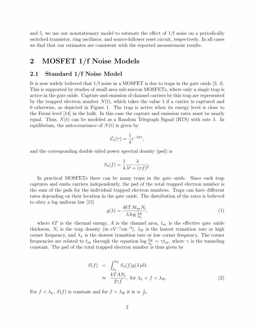
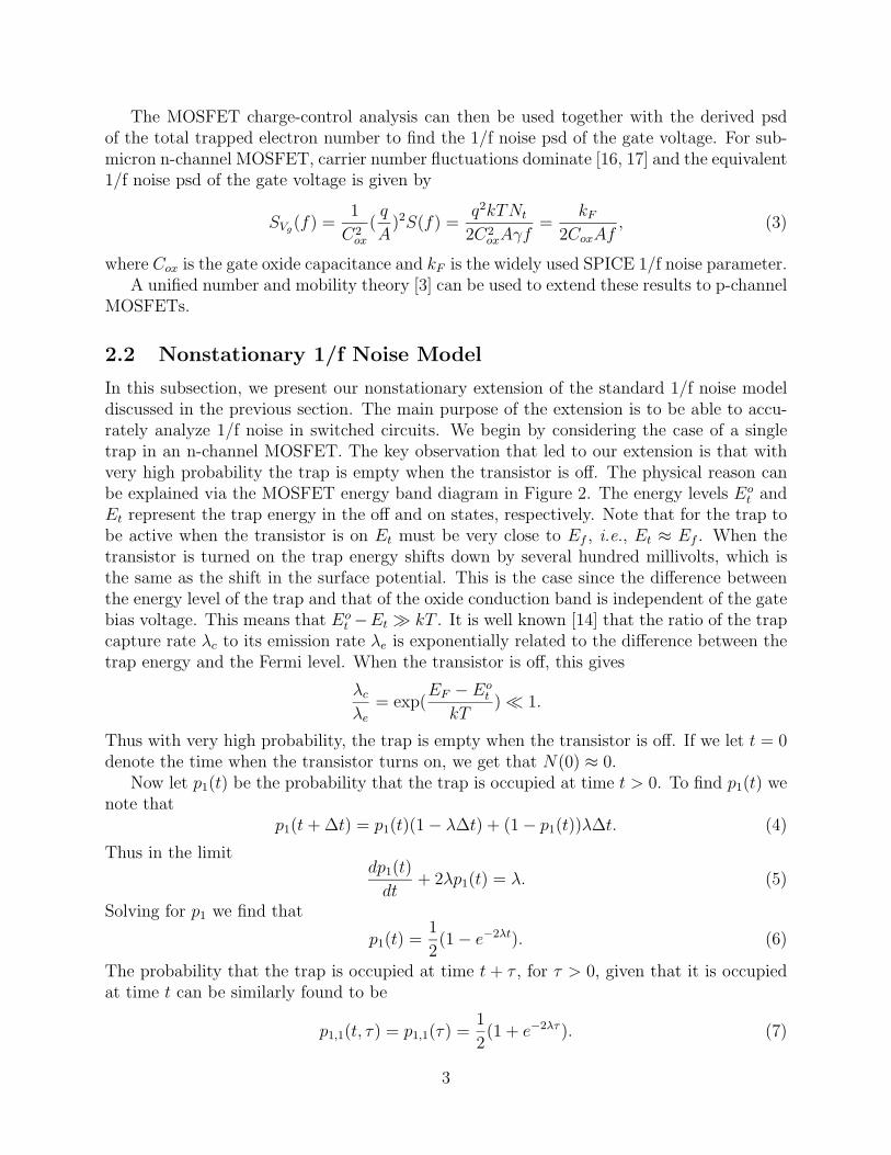
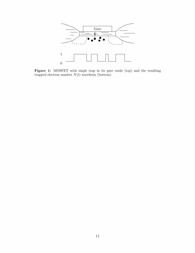
It is now widely believed that 1/f noise in a MOSFET is due to traps in the gate oxide [3, 4].This is supported by studies of small area sub-micron MOSFETs, where only a single trap isactive in the gate oxide. Capture and emission of channel carriers by this trap are representedby the trapped electron number N(t), which takes the value 1 if a carrier is captured and0 otherwise, as depicted in Figure 1. The trap is active when its energy level is close tothe Fermi level [14] in the bulk. In this case the capture and emission rates must be nearlyequal. Thus, N(t) can be modeled as a Random Telegraph Signal (RTS) with rate λ. Inequilibrium, the autocovariance of N(t) is given by
Cλ(τ) = 1
4e−2λτ ,
and the corresponding double sided power spectral density (psd) is
Sλ(f) =1
4
λ
λ2 + (πf)2.
In practical MOSFETs there can be many traps in the gate oxide. Since each trapcaptures and emits carriers independently, the psd of the total trapped electron number isthe sum of the psds for the individual trapped electron numbers. Traps can have differentrates depending on their location in the gate oxide. The distribution of the rates is believedto obey a log uniform law [15]
g(λ) =4kTAtoxNt
λ log λH
λL
, (1)
where kT is the thermal energy, A is the channel area, tox is the effective gate oxidethickness, Nt is the trap density (in eV−1cm−3), λH is the fastest transition rate or highcorner frequency, and λL is the slowest transition rate or low corner frequency. The cornerfrequencies are related to tox through the equation log λH
λL= γtox, where γ is the tunneling
constant. The psd of the total trapped electron number is thus given by
S(f) =∫ λH
λL
Sλ(f)g(λ)dλ
≈ kTANt2γf
, for λL < f < λH . (2)
For f < λL, S(f) is constant and for f > λH it is ∝ 1f2 .
2
The MOSFET charge-control analysis can then be used together with the derived psdof the total trapped electron number to find the 1/f noise psd of the gate voltage. For sub-micron n-channel MOSFET, carrier number fluctuations dominate [16, 17] and the equivalent1/f noise psd of the gate voltage is given by
SVg(f) =1
C2ox
(q
A)2S(f) =
q2kTNt2C2
oxAγf=
kF2CoxAf
, (3)
where Cox is the gate oxide capacitance and kF is the widely used SPICE 1/f noise parameter.A unified number and mobility theory [3] can be used to extend these results to p-channel
MOSFETs.
2.2 Nonstationary 1/f Noise Model
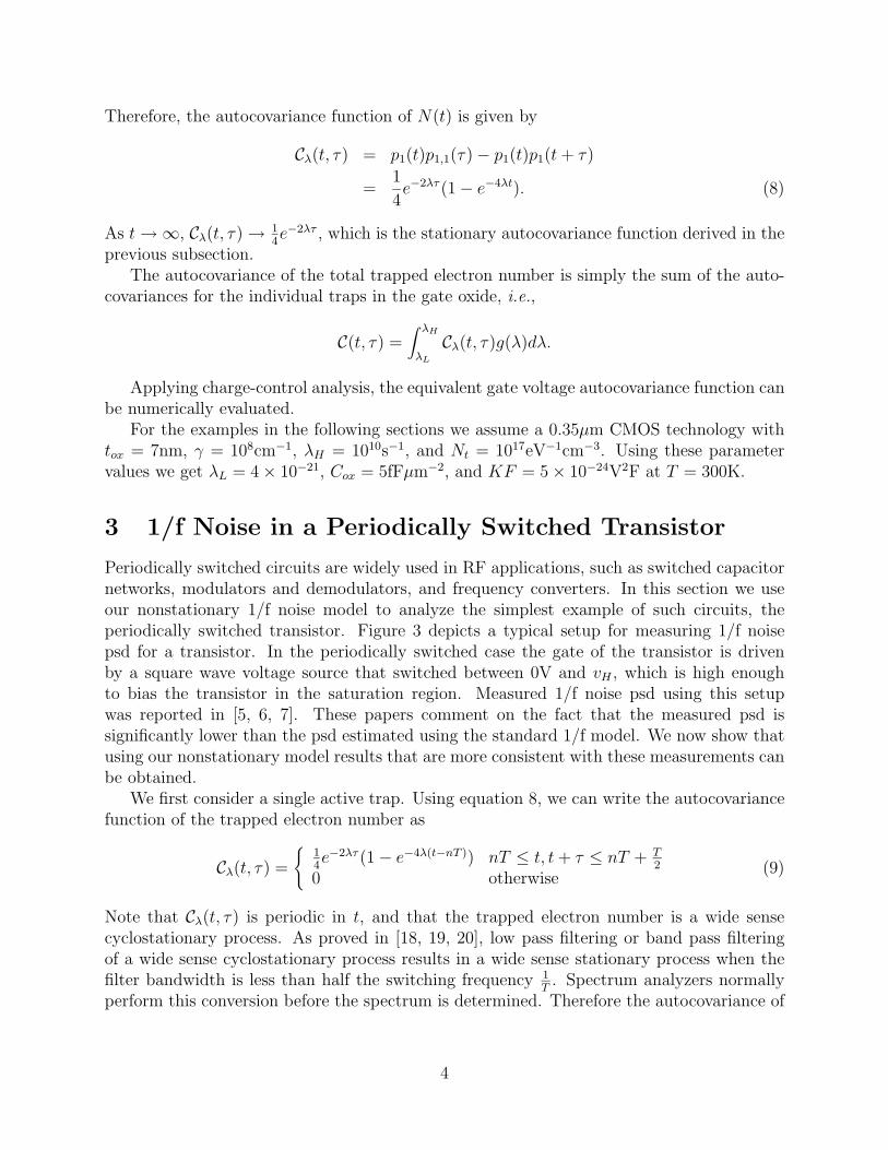
In this subsection, we present our nonstationary extension of the standard 1/f noise modeldiscussed in the previous section. The main purpose of the extension is to be able to accu-rately analyze 1/f noise in switched circuits. We begin by considering the case of a singletrap in an n-channel MOSFET. The key observation that led to our extension is that withvery high probability the trap is empty when the transistor is off. The physical reason canbe explained via the MOSFET energy band diagram in Figure 2. The energy levels Eot andEt represent the trap energy in the off and on states, respectively. Note that for the trap tobe active when the transistor is on Et must be very close to Ef , i.e., Et ≈ Ef . When thetransistor is turned on the trap energy shifts down by several hundred millivolts, which isthe same as the shift in the surface potential. This is the case since the difference betweenthe energy level of the trap and that of the oxide conduction band is independent of the gatebias voltage. This means that Eot −Et � kT . It is well known [14] that the ratio of the trapcapture rate λc to its emission rate λe is exponentially related to the difference between thetrap energy and the Fermi level. When the transistor is off, this gives
λcλe
= exp(EF − Eot
kT) � 1.
Thus with very high probability, the trap is empty when the transistor is off. If we let t = 0denote the time when the transistor turns on, we get that N(0) ≈ 0.
Now let p1(t) be the probability that the trap is occupied at time t > 0. To find p1(t) wenote that
p1(t+∆t) = p1(t)(1− λ∆t) + (1− p1(t))λ∆t. (4)
Thus in the limitdp1(t)
dt+ 2λp1(t) = λ. (5)
Solving for p1 we find that
p1(t) =1
2(1− e−2λt). (6)
The probability that the trap is occupied at time t + τ , for τ > 0, given that it is occupiedat time t can be similarly found to be
p1,1(t, τ) = p1,1(τ) =1
2(1 + e−2λτ ). (7)
3
Therefore, the autocovariance function of N(t) is given by
Cλ(t, τ) = p1(t)p1,1(τ)− p1(t)p1(t+ τ)
=1
4e−2λτ (1− e−4λt). (8)
As t → ∞, Cλ(t, τ) → 14e−2λτ , which is the stationary autocovariance function derived in the
previous subsection.The autocovariance of the total trapped electron number is simply the sum of the auto-
covariances for the individual traps in the gate oxide, i.e.,
C(t, τ) =∫ λH
λL
Cλ(t, τ)g(λ)dλ.
Applying charge-control analysis, the equivalent gate voltage autocovariance function canbe numerically evaluated.
For the examples in the following sections we assume a 0.35µm CMOS technology withtox = 7nm, γ = 108cm−1, λH = 1010s−1, and Nt = 1017eV−1cm−3. Using these parametervalues we get λL = 4× 10⁻²¹, Cox = 5fFµm−2, and KF = 5× 10⁻²⁴V2F at T = 300K.
3 1/f Noise in a Periodically Switched Transistor
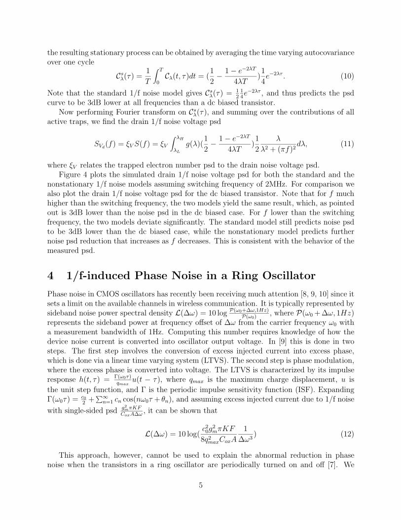
Periodically switched circuits are widely used in RF applications, such as switched capacitornetworks, modulators and demodulators, and frequency converters. In this section we useour nonstationary 1/f noise model to analyze the simplest example of such circuits, theperiodically switched transistor. Figure 3 depicts a typical setup for measuring 1/f noisepsd for a transistor. In the periodically switched case the gate of the transistor is drivenby a square wave voltage source that switched between 0V and vH , which is high enoughto bias the transistor in the saturation region. Measured 1/f noise psd using this setupwas reported in [5, 6, 7]. These papers comment on the fact that the measured psd issignificantly lower than the psd estimated using the standard 1/f model. We now show thatusing our nonstationary model results that are more consistent with these measurements canbe obtained.
We first consider a single active trap. Using equation 8, we can write the autocovariancefunction of the trapped electron number as
Cλ(t, τ) ={
14e−2λτ (1− e−4λ(t−nT )) nT ≤ t, t+ τ ≤ nT + T
2
0 otherwise(9)
Note that Cλ(t, τ) is periodic in t, and that the trapped electron number is a wide sensecyclostationary process. As proved in [18, 19, 20], low pass filtering or band pass filteringof a wide sense cyclostationary process results in a wide sense stationary process when thefilter bandwidth is less than half the switching frequency 1
T. Spectrum analyzers normally
perform this conversion before the spectrum is determined. Therefore the autocovariance of
4
the resulting stationary process can be obtained by averaging the time varying autocovarianceover one cycle
Csλ(τ) =1
T
∫ T
0Cλ(t, τ)dt = (
1
2− 1− e−2λT
4λT)1
4e−2λτ . (10)
Note that the standard 1/f noise model gives Csλ(τ) = 12
14e−2λτ , and thus predicts the psd
curve to be 3dB lower at all frequencies than a dc biased transistor.Now performing Fourier transform on Csλ(τ), and summing over the contributions of all
active traps, we find the drain 1/f noise voltage psd
SVd(f) = ξV S(f) = ξV
∫ λH
λL
g(λ)(1
2− 1− e−2λT
4λT)1
2
λ
λ2 + (πf)2dλ, (11)
where ξV relates the trapped electron number psd to the drain noise voltage psd.Figure 4 plots the simulated drain 1/f noise voltage psd for both the standard and the
nonstationary 1/f noise models assuming switching frequency of 2MHz. For comparison wealso plot the drain 1/f noise voltage psd for the dc biased transistor. Note that for f muchhigher than the switching frequency, the two models yield the same result, which, as pointedout is 3dB lower than the noise psd in the dc biased case. For f lower than the switchingfrequency, the two models deviate significantly. The standard model still predicts noise psdto be 3dB lower than the dc biased case, while the nonstationary model predicts furthernoise psd reduction that increases as f decreases. This is consistent with the behavior of themeasured psd.
4 1/f-induced Phase Noise in a Ring Oscillator
Phase noise in CMOS oscillators has recently been receiving much attention [8, 9, 10] since itsets a limit on the available channels in wireless communication. It is typically represented bysideband noise power spectral density L(∆ω) = 10 log P(ω0+∆ω,1Hz)
P(ω0), where P(ω0 +∆ω, 1Hz)
represents the sideband power at frequency offset of ∆ω from the carrier frequency ω0 witha measurement bandwidth of 1Hz. Computing this number requires knowledge of how thedevice noise current is converted into oscillator output voltage. In [9] this is done in twosteps. The first step involves the conversion of excess injected current into excess phase,which is done via a linear time varying system (LTVS). The second step is phase modulation,where the excess phase is converted into voltage. The LTVS is characterized by its impulseresponse h(t, τ) = Γ(ω0τ)
qmaxu(t − τ), where qmax is the maximum charge displacement, u is
the unit step function, and Γ is the periodic impulse sensitivity function (ISF). ExpandingΓ(ω0τ) =
c02+
∑∞n=1 cn cos(nω0τ + θn), and assuming excess injected current due to 1/f noise
with single-sided psd g2mπKFCoxA∆ω
, it can be shown that
L(∆ω) = 10 log(c20g
2mπKF
8q2maxCoxA
1
∆ω3) (12)
This approach, however, cannot be used to explain the abnormal reduction in phasenoise when the transistors in a ring oscillator are periodically turned on and off [7]. We
5
now show that using our nonstationary 1/f noise model, we can explain this reduction. Inthese experiments, one transistor typically has much smaller area than the rest, and thusits 1/f-induced phase noise dominates. To study the noise due to this transistor, we firstconsider the case where there is only one active trap inside its gate oxide. Using the periodicautocovariance function of the trapped electron number as expressed in equation 9, we canfind the time varying psd [21]
S(t, f) =
{12
λλ2+(πf)2
(1− e−4λ(t−nT )) nT ≤ t, t+ τ ≤ nT + T2,
0 otherwise,(13)
where T = 2πω0. Note that the function S(t, f) is separable and can thus be expressed as
S(f)α(ω0t), where S(f) = 12
λλ2+(πf)2
and α(ω0t) is a periodic function. For this class of
cyclostationary noise sources, it is shown in [9] that phase noise can still be calculated usingequation 12, with S(f) representing a stationary noise source which is associated with aneffective ISF Γeff = Γ(ω0t)α(ω0t). In [9] it is also shown that for independent noise sourcesthe total phase noise is simply the sum of the phase noise due to each source. We can use thisfact to find the 1/f-induced phase noise psd in the case of many traps, since their trappedelectron numbers are independent.
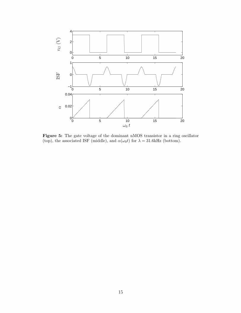
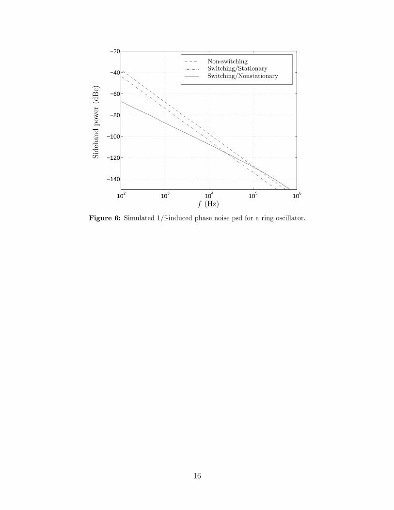
To demonstrate that our nonstationary 1/f noise model can be used to explain the reduc-tion in phase noise consider a ring oscillator with the ISF shown in Figure 5. The figure alsoplots the gate voltage for the transistor under consideration. Figure 6 plots the simulatedphase noise psd using both the nonstationary and the standard 1/f noise models at 2MHzswitching frequency. We also plot the phase noise psd of a non-switching ring oscillator,where the transistor is always on. As can be seen, the standard 1/f noise model reportsphase noise that is 6dBc lower than the non-switching case, at all frequencies. The 6dBcreduction, however, is too small when compared to the reported measurements [7], whichshow over 10dBc reduction in the 1-10kHz range. By comparison, the plot using our nonsta-tionary model shows 10-20dBc reduction in this frequency range. The reduction is the resultof the decrease in 1/f noise due to the switching of the transistor as discussed in the previoussection. Note that our model predicts an increase in 1/f-induced phase noise above 100kHzrelative to the estimates of the standard model. This, we believe, is due to the nonflat shapeof the α(ω0t) as shown in Figure 5, which can cause significant asymmetry in the effectiveISF Γeff , and thus can increase phase noise.
5 1/f Noise in Source Follower Reset Circuit
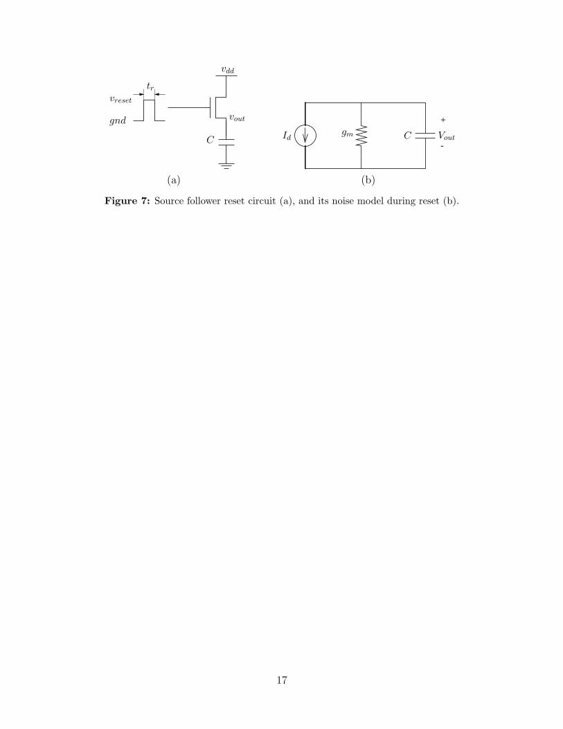
The source follower reset circuit is commonly used in the output stage of a CCD image sensorand the pixel circuit of a CMOS APS. As depicted in Figure 7 during reset, the gate of thetransistor is set to a high voltage vreset for a short period of time tr. To find the output noisepower due to the transistor 1/f noise, frequency domain analysis is typically performed usingthe standard 1/f noise model to get
V 2out(tr) =
∫ ∞1tr
SId(f)
g2m(tr) + 4π2f 2C2
df,
6
where gm is the transistor transconductance, and SId is the transistor drain current 1/fnoise psd. The choice of 1
tras a low cutoff frequency is quite arbitrary, however. Moreover
the circuit is not in steady state [22] and thus it is not appropriate to use frequency domainanalysis.
In this section we use our nonstationary 1/f noise model and time domain analysis toobtain more accurate noise power estimates. First note that at the beginning of reset, thetransistor is either operating in the saturation region or in subthreshold depending on thevalue of vout. Even if the transistor is first in in saturation, it quickly goes into subthresholdand does not reach steady state. This was explained in detail in [22], where we analyzedreset noise due to thermal and shot noise sources. The circuit noise model during reset isshown in Figure 7 (b). The current source Id(t) models the transistor 1/f noise and gm isthe transistor transconductance in subthreshold, which is time varying. The output noisevoltage at the end of reset is given by [22]
Vout(tr) =∫ tr
0
Id(s)
Ce−
∫ tr
s
gm(τ)C
dτds, (14)
The output reset noise power is thus given by
V 2out(tr) = (
q
ACoxC)2
∫ tr
0
∫ tr
0gm(s1)gm(s2)C(s1, |s2−s1|)e−
1C
∫ tr
s1gm(τ1)dτ1
e− 1
C
∫ tr
s2gm(τ2)dτ2
ds1ds2.
(15)Using the MOS transistor subthreshold I–V characteristics, we get that gm(τ) ≈ C
τ+δ,
where δ is the thermal time [22]. Thus
e−1C
∫ tr
sgr(τ)dτ ≈ s+ δ
tr + δ.
Substituting this and equation 1 and 8 into equation 15, we get that
V 2out(tr) = (
q
ACox)2
1
(tr + δ)2
∫ tr
0
∫ tr
0
∫ λH
λL
Cλ(s1, |s2 − s1|)g(λ)dλds1ds2. (16)
Note that this result is virtually independent of the capacitance. This of course is verydifferent from the famous kT/C reset noise due to thermal and shot noise sources. Thereason is that 1/f noise power is concentrated on low frequencies, and thus is less sensitiveto circuit bandwidth and hence C.
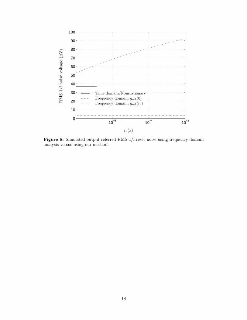
In Figure 8 we compare the results using our method to the results using conventionalfrequency domain analysis. To perform the frequency domain analysis we need to decide onthe value of gm to use. In that figure we plot the results of the frequency domain analysis fortwo values of gm, one at the beginning and the other at the end of the reset time. Note theenormous difference between the curves for the two gm values. Depending on which gm valueis used, the results can vary from 3.2µV to 68µV at tr = 10µs. This presents yet anotherserious shortcoming of using frequency domain analysis.
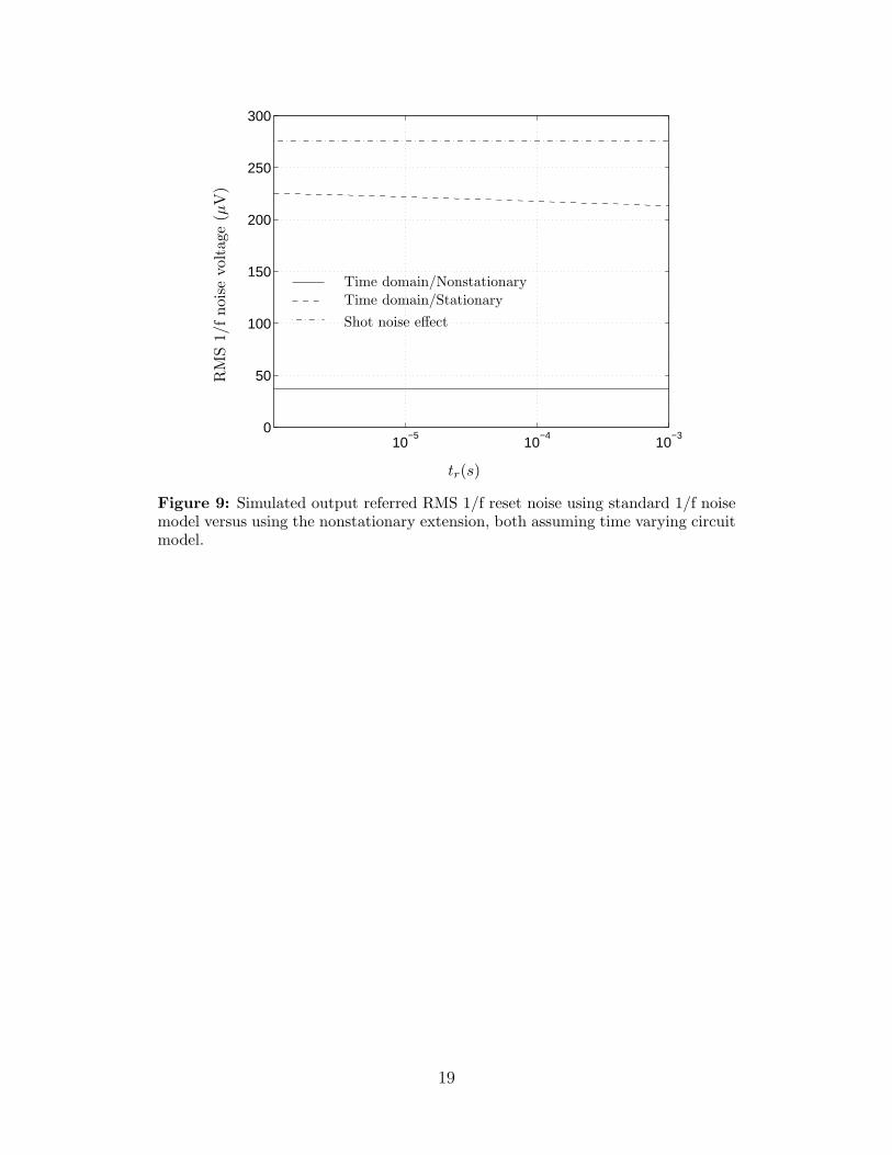
To isolate the effect of using the standard versus the nonstationary noise models, inFigure 9 we plot the curves for both models using the same time varying circuit model. Incalculating the noise assuming the standard model we simply replace the Cλ(s1, |s2 − s1|) in
7
equation 16 by the stationary autocovariance Cλ(|s2 − s1|). As can be seen from the twocurves, the RMS noise voltage using the standard model is much higher, e.g., 222µV versus37.2µV at tr = 10µs. The noise due to reset transistor shot noise is also plotted and isaround 276µV. Note that the RMS 1/f noise voltage predicted by the standard model iscomparable to the effect of the shot noise. Measurement results [22, 23] show however thatshot noise dominates the reset noise, which corroborates the analysis using our method.
6 Conclusion
Recent experimental results showed that the estimates of the effect of 1/f noise obtained usingthe standard 1/f noise model can be quite inaccurate especially for switched circuits. In thecase of a periodically switched transistor measured 1/f noise psd was shown to be significantlylower than the estimate using the standard 1/f noise model. Similarly, measured 1/f-inducedphase noise psd in a ring oscillator was also shown to be significantly lower than the estimatesusing the standard 1/f noise model. To find the output noise power due to 1/f noise in a sourcefollower reset circuit, frequency domain analysis is typically performed using the standard1/f noise model. A low cutoff frequency that is inversely proportional to the circuit on-timeis typically used to obtain reasonable noise power estimates. The choice of this low cutofffrequency is quite arbitrary, however, and can cause significant inaccuracy in estimatingnoise power. Moreover, during reset the circuit is not in steady state and thus frequencydomain analysis does not apply. We used our nonstationary extension of the standard 1/fnoise model to analyze the effect of 1/f noise in these three switched circuit examples. In allcases we obtained results that are more consistent with reported measurements than thoseobtained using the standard 1/f noise model. This not only validates our model but alsomeans that accurate estimates of the effect of 1/f noise on MOSFET circuits can now beobtained for a wider range of applications.
7 Acknowledgments
The authors would like to thank T. Chen, S.H. Lim, X. Liu, and K. Salama for the helpfuldiscussions.
8
References
[1] P.R. Gray and R.G. Meyer, Analysis and Design of Analog Integrated Circuits, John Wiley &Sons, Inc., New York, 1993.
[2] C. Hu, G. P. Li, E. Worley, and J. White, “Consideration of Low-Frequency Noise in MOS-FET’s for Analog Performance,” IEEE Electron Device Letters, vol. 17, no. 12, pp. 552–554,December 1996.
[3] K. K. Hung, P. K. Ko, C. Hu, and Y. C. Cheng, “A Unified Model for the Flicker Noise inMetal-Oxide-Semiconductor Field-Effect Transistors,” IEEE Trans. Electron Device, vol. 37,no. 3, pp. 654–665, March 1990.
[4] C. Jakobson, I. Bloom, and Y. Nemirovsky, “1/f Noise in CMOS Transistors for AnalogApplications From Subthreshod to Saturation,” Solid-State Electronics, vol. 42, no. 10, pp.1807–1817, 1998.
[5] I. Bloom and Y. Nemirovsky, “1/f Noise Reduction of Metal-Oxide-Semiconductor Transistorsby Cycling From Inversion to Accumulation,” Applied Physics Letters, vol. 58, no. 15, pp.1664–1666, April 1991.
[6] B. Dierickx and E. Simoen, “The Decrease of ”Random Telegraph Signal” Noise in Metal-Oxide-Semiconductor Field-Effect Transistors When Cycled From Inversion to Accumulation,”J. Applied Physics, vol. 71, no. 4, pp. 2028–2029, February 1992.
[7] S. L. J. Gierkink, E. A. M. Klumperink, A. P. van der Wel, G. Hoogzaad, E. van Tuijl, andB. Nauta, “Intrinsic 1/f Device Noise Reduction and Its Effect on Phase Noise in CMOS RingOscillators,” IEEE J. Solid-State Circuits, vol. 34, no. 7, pp. 1022–1025, July 1999.
[8] A. Hajimiri, S. Limotyrakis, and T. H. Lee, “Jitter and Phase Noise in Ring Oscillators,”IEEE J. Solid-State Circuits, vol. 34, no. 6, pp. 790–804, June 1999.
[9] A. Hajimiri and T. H. Lee, “A General Theory of Phase Noise in Electrical Oscillators,” IEEEJ. Solid-State Circuits, vol. 33, no. 2, pp. 179–194, February 1998.
[10] B. Razavi, “A Study of Phase Noise in CMOS Oscillators,” IEEE J. Solid-State Circuits, vol.31, no. 3, pp. 331–343, March 1996.
[11] A. J. P. Theuwissen, Solid-State Imaging with Charge-Coupled Devices, Kluwer AcademicPublishers, 1995.
[12] E. R. Fossum, “CMOS Image Sensors: Electronic Camera-on-a-chip,” IEEE Transactions onElectron Devices, vol. 44, no. 10, pp. 1689–1698, October 1997.
[13] H. Tian and A. El Gamal, “Analysis of 1/f Noise in CMOS APS,” in Proc. SPIE, San Jose,CA, Jan. 2000, vol. 3965.
[14] M. J. Kirton and M. J. Uren, “Noise in Solid-State Microstructures: A New Perspective onIndividual Defects, Interface States and Low-frequency (1/f) Noise,” Advances in Physics, vol.38, no. 4, pp. 367–468, 1989.
[15] A. van der Ziel, Noise in Solid State Devices and Circuits, Wiley, 1986.
[16] J. Chang, A. A. Abidi, and C. R. Viswanathan, “Flicker Noise in CMOS Transistors fromSubthreshold to Strong Inversion at Various Temperatures,” IEEE Trans. Electron Device,vol. 41, no. 11, pp. 1965–1971, November 1994.
9
[17] T. Boutchacha, G. Ghibaudo, G. Guegan, and T. Skotnicki, “Low Frequency Noise Charac-terization of 0.18um Si CMOS Transistors,” Microelectron. Reliab., vol. 37, no. 10/11, pp.1599–1602, 1997.
[18] T. Strom and S. Signell, “Analysis of Periodically Switched Linear Circuits,” IEEE Trans.Circuits Syst., vol. 24, no. 10, pp. 531–541, October 1977.
[19] C. D. Hull and R. G. Meyer, “A Systematic Approach to the Analysis of Noise in Mixers,”IEEE Trans. Circuits Syst., vol. 40, no. 12, pp. 909–919, December 1993.
[20] J. Roychowdhury, D. Long, and P. Feldmann, “Cyclostationary Noise Analysis of Large RFCircuits with Multitone Excitations,” IEEE J. Solid-State Circuits, vol. 33, no. 3, pp. 324–336,March 1998.
[21] D. G. Lampard, “Generalization of the Wiener-Khintchine Theorem to Nonstationary Pro-cesses,” J. Applied Physics, vol. 25, no. 6, pp. 802–803, June 1954.
[22] H. Tian, B. Fowler, and A. El Gamal, “Analysis of Temporal Noise in CMOS APS,” in Proc.SPIE, San Jose, CA, Jan. 1999, vol. 3649, pp. 177–185.
[23] R. Sarpeshkar, T. Delbruck, and C.A. Mead, “White Noise in MOS Transistors and Resistors,”IEEE Circuits and Devices Magazine, vol. 9, no. 6, pp. 23–29, November 1993.
10
Gate
1
0
Figure 1: MOSFET with single trap in its gate oxide (top) and the resultingtrapped electron number N(t) waveform (bottom).
11
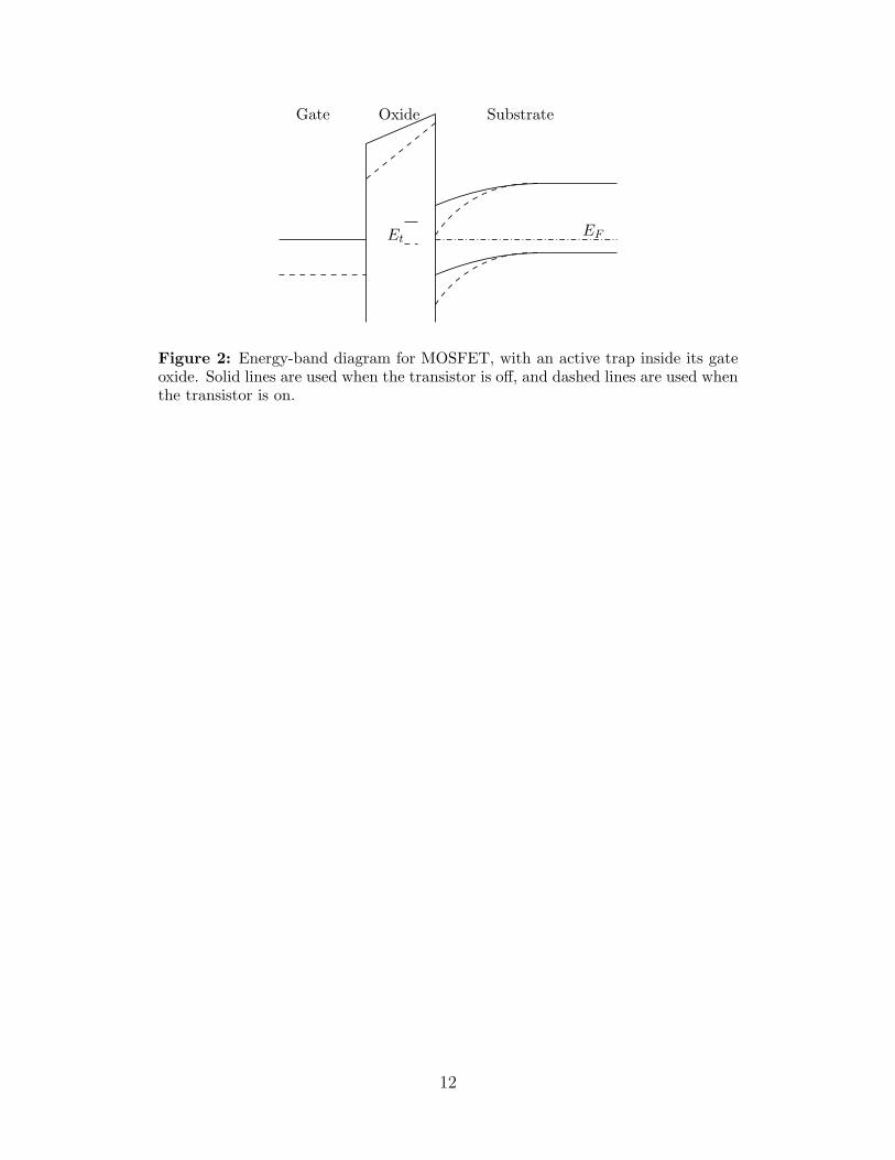
Et EF
SubstrateOxideGate
Figure 2: Energy-band diagram for MOSFET, with an active trap inside its gateoxide. Solid lines are used when the transistor is off, and dashed lines are used whenthe transistor is on.
12
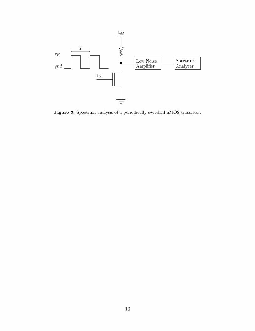
vdd
vH
gnd
T
vG
Low NoiseAmplifier
SpectrumAnalyzer
Figure 3: Spectrum analysis of a periodically switched nMOS transistor.
13
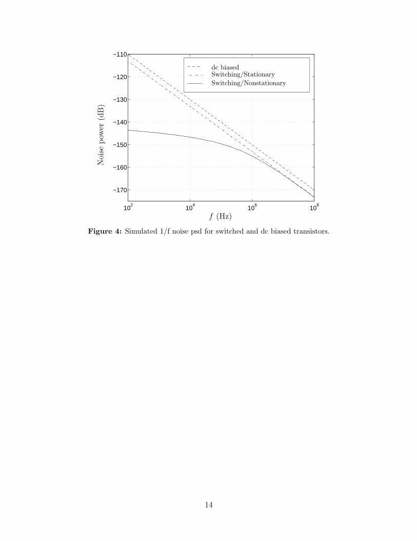
102
104
106
108
−170
−160
−150
−140
−130
−120
−110
f (Hz)
Noise
pow
er(dB)
Switching/NonstationarySwitching/Stationarydc biased
Figure 4: Simulated 1/f noise psd for switched and dc biased transistors.
14
0 5 10 15 20
0
2
4
0 5 10 15 20−1
0
1
0 5 10 15 200
0.02
0.04
ω0 t
v G(V
)ISF
α
Figure 5: The gate voltage of the dominant nMOS transistor in a ring oscillator(top), the associated ISF (middle), and α(ω0t) for λ = 31.6kHz (bottom).
15
102
103
104
105
106
−140
−120
−100
−80
−60
−40
−20
f (Hz)
Sideban
dpow
er(dBc)
Switching/NonstationarySwitching/StationaryNon-switching
Figure 6: Simulated 1/f-induced phase noise psd for a ring oscillator.
16
trvreset
gnd
vdd
vout
C
+
-Id
gm C Vout
(a) (b)
Figure 7: Source follower reset circuit (a), and its noise model during reset (b).
17
10−5
10−4
10−3
0
10
20
30
40
50
60
70
80
90
100
tr(s)
RM
S1/
fno
ise
volt
age
(µV
)
Time domain/NonstationaryFrequency domain, gm1(0)Frequency domain, gm1(tr)
Figure 8: Simulated output referred RMS 1/f reset noise using frequency domainanalysis versus using our method.
18
10−5
10−4
10−3
0
50
100
150
200
250
300
tr(s)
RM
S1/
fno
ise
volt
age
(µV
)
Time domain/NonstationaryTime domain/StationaryShot noise effect
Figure 9: Simulated output referred RMS 1/f reset noise using standard 1/f noisemodel versus using the nonstationary extension, both assuming time varying circuitmodel.
19