an5050 application note · application note octo-spi interface on stm32 microcontrollers...
TRANSCRIPT

April 2020 AN5050 Rev 5 1/73
1
AN5050Application note
Octo-SPI interface on STM32 microcontrollers
Introduction
The growing demand for richer graphics, wider range of multimedia and other data-intensive content, drives embedded designers to enable more sophisticated features in embedded applications. These sophisticated features require higher data throughputs and extra demands on the often limited MCU on-chip memory.
External parallel memories have been widely used so far to provide higher data throughput and to extend the MCU on-chip memory, solving the memory size and the performance limitation. However, this action compromises the pin count and implies a need of more complex designs and higher cost.
To meet these requirements, STMicroelectronics offers several MCU products in the market with the new integrated high-throughput Octo-SPI interface (see the table below).
The Octo-SPI interface enables the connection of the external compact-footprint Octo-SPI and the HyperBus™ high-speed volatile and non-volatile memories available today in the market. Thanks to its low-pin count, the Octo-SPI interface allows easier PCB designs and lower costs. Its high throughput allows in place code execution (XIP) and data storage.
Thanks to the Octo-SPI memory-mapped mode, the external memory can be accessed as if it was an internal memory allowing the system masters (such as DMA, LTDC, DMA2D, GFXMMU or SDMMC) to access autonomously even in low-power mode when the CPU is stopped, which is ideal for mobile and wearable applications
This application note describes the OCTOSPI peripheral in STM32 MCUs and explains how to configure it in order to write and read external Octo-SPI and HyperBus™ memories. This document describes some typical use cases to use the Octo-SPI interface and provides some practical examples on how to configure the OCTOSPI peripheral depending on the type of the targeted memory.
Related documents
Available from STMicroelectronics web site www.st.com:
• reference manuals and datasheets for STM32 devices
• application note Quad-SPI interface on STM32 microcontrollers (AN4760)
Table 1. Applicable products
Type Series or line
MicrocontrollersSTM32L4+ Series, STM32L5 Series
STM32H7A3/B3 line
www.st.com

Contents AN5050
2/73 AN5050 Rev 5
Contents
1 Overview of the OCTOSPI in STM32 MCUs . . . . . . . . . . . . . . . . . . . . . . 6
1.1 OCTOSPI main features . . . . . . . . . . . . . . . . . . . . . . . . . . . . . . . . . . . . . . 6
1.2 OCTOSPI in a smart architecture . . . . . . . . . . . . . . . . . . . . . . . . . . . . . . . . 7
1.2.1 STM32L4+ Series system architecture . . . . . . . . . . . . . . . . . . . . . . . . . . 7
1.2.2 STM32L5 Series system architecture . . . . . . . . . . . . . . . . . . . . . . . . . . . 9
1.2.3 STM32H7A3/B3 system architecture . . . . . . . . . . . . . . . . . . . . . . . . . . . 10
2 Octo-SPI interface description . . . . . . . . . . . . . . . . . . . . . . . . . . . . . . . . 11
2.1 OCTOSPI hardware interface . . . . . . . . . . . . . . . . . . . . . . . . . . . . . . . . . .11
2.1.1 OCTOSPI pins and signal interface . . . . . . . . . . . . . . . . . . . . . . . . . . . . 11
2.1.2 OCTOSPI delay block . . . . . . . . . . . . . . . . . . . . . . . . . . . . . . . . . . . . . . 11
2.2 Two low-level protocols . . . . . . . . . . . . . . . . . . . . . . . . . . . . . . . . . . . . . . 12
2.2.1 Regular-command protocol . . . . . . . . . . . . . . . . . . . . . . . . . . . . . . . . . . 12
2.2.2 HyperBus protocol . . . . . . . . . . . . . . . . . . . . . . . . . . . . . . . . . . . . . . . . . 13
2.3 Three operating modes . . . . . . . . . . . . . . . . . . . . . . . . . . . . . . . . . . . . . . 15
2.3.1 Indirect mode . . . . . . . . . . . . . . . . . . . . . . . . . . . . . . . . . . . . . . . . . . . . . 15
2.3.2 Status-flag polling mode . . . . . . . . . . . . . . . . . . . . . . . . . . . . . . . . . . . . 15
2.3.3 Memory-mapped mode . . . . . . . . . . . . . . . . . . . . . . . . . . . . . . . . . . . . . 15
3 OCTOSPI I/O manager . . . . . . . . . . . . . . . . . . . . . . . . . . . . . . . . . . . . . . 17
4 OCTOSPI configuration . . . . . . . . . . . . . . . . . . . . . . . . . . . . . . . . . . . . . 19
4.1 OCTOSPI common configuration . . . . . . . . . . . . . . . . . . . . . . . . . . . . . . . 19
4.1.1 GPIOs and OCTOSPI I/Os configuration . . . . . . . . . . . . . . . . . . . . . . . . 19
4.1.2 Interrupts and clocks configuration . . . . . . . . . . . . . . . . . . . . . . . . . . . . 21
4.2 OCTOSPI configuration for regular-command protocol . . . . . . . . . . . . . . 23
4.3 OCTOSPI configuration for HyperBus protocol . . . . . . . . . . . . . . . . . . . . 23
4.4 Memory configuration . . . . . . . . . . . . . . . . . . . . . . . . . . . . . . . . . . . . . . . . 24
4.4.1 Octo-SPI memory device configuration . . . . . . . . . . . . . . . . . . . . . . . . . 24
4.4.2 HyperBus memory device configuration . . . . . . . . . . . . . . . . . . . . . . . . 24
5 OCTOSPI application examples . . . . . . . . . . . . . . . . . . . . . . . . . . . . . . . 25
5.1 Implementation examples . . . . . . . . . . . . . . . . . . . . . . . . . . . . . . . . . . . . 25
5.1.1 Using OCTOSPI in a graphical application . . . . . . . . . . . . . . . . . . . . . . 25

AN5050 Rev 5 3/73
AN5050 Contents
3
5.1.2 Executing from external memory: extend internal memory size . . . . . . 26
5.2 OCTOSPI configuration with STM32CubeMX . . . . . . . . . . . . . . . . . . . . . 27
5.2.1 Hardware description . . . . . . . . . . . . . . . . . . . . . . . . . . . . . . . . . . . . . . . 27
5.2.2 Use case description . . . . . . . . . . . . . . . . . . . . . . . . . . . . . . . . . . . . . . . 29
5.2.3 OCTOSPI GPIOs and clocks configuration . . . . . . . . . . . . . . . . . . . . . . 30
5.2.4 OCTOSPI configuration and parameter settings . . . . . . . . . . . . . . . . . . 36
5.2.5 STM32CubeMX: Project generation . . . . . . . . . . . . . . . . . . . . . . . . . . . 39
6 Performance and power . . . . . . . . . . . . . . . . . . . . . . . . . . . . . . . . . . . . . 67
6.1 How to get the best read performance . . . . . . . . . . . . . . . . . . . . . . . . . . . 67
6.2 Decreasing power consumption . . . . . . . . . . . . . . . . . . . . . . . . . . . . . . . . 67
6.2.1 STM32 low-power modes . . . . . . . . . . . . . . . . . . . . . . . . . . . . . . . . . . . 68
6.2.2 Decreasing Octo-SPI memory power consumption . . . . . . . . . . . . . . . . 68
7 Supported devices . . . . . . . . . . . . . . . . . . . . . . . . . . . . . . . . . . . . . . . . . 70
8 Conclusion . . . . . . . . . . . . . . . . . . . . . . . . . . . . . . . . . . . . . . . . . . . . . . . . 70
9 Revision history . . . . . . . . . . . . . . . . . . . . . . . . . . . . . . . . . . . . . . . . . . . 71

List of tables AN5050
4/73 AN5050 Rev 5
List of tables
Table 1. Applicable products . . . . . . . . . . . . . . . . . . . . . . . . . . . . . . . . . . . . . . . . . . . . . . . . . . . . . . . 1Table 2. OCTOSPI main features. . . . . . . . . . . . . . . . . . . . . . . . . . . . . . . . . . . . . . . . . . . . . . . . . . . . 6Table 3. STM32CubeMx - Memory connection port . . . . . . . . . . . . . . . . . . . . . . . . . . . . . . . . . . . . . 30Table 4. STM32CubeMx - OCTOSPI mode . . . . . . . . . . . . . . . . . . . . . . . . . . . . . . . . . . . . . . . . . . . 31Table 5. STM32CubeMx - Configuration of OCTOSPI parameters . . . . . . . . . . . . . . . . . . . . . . . . . 37Table 6. OCTOSPI states in different power modes on STM32L4+ and STM32L5 Series . . . . . . . 68Table 7. Document revision history . . . . . . . . . . . . . . . . . . . . . . . . . . . . . . . . . . . . . . . . . . . . . . . . . 71
AN5050 Rev 5 5/73
AN5050 List of figures
5
List of figures
Figure 1. STM32L4+ Series system architecture. . . . . . . . . . . . . . . . . . . . . . . . . . . . . . . . . . . . . . . . . 8Figure 2. STM32L5 Series system architecture. . . . . . . . . . . . . . . . . . . . . . . . . . . . . . . . . . . . . . . . . . 9Figure 3. STM32H7A3/B3 system architecture . . . . . . . . . . . . . . . . . . . . . . . . . . . . . . . . . . . . . . . . . 10Figure 4. OCTOSPI delay block. . . . . . . . . . . . . . . . . . . . . . . . . . . . . . . . . . . . . . . . . . . . . . . . . . . . . 12Figure 5. Regular-command mode: octal DTR read operation example
in Macronix mode . . . . . . . . . . . . . . . . . . . . . . . . . . . . . . . . . . . . . . . . . . . . . . . . . . . . . . . . 13Figure 6. HyperBus protocol: example of reading operation from HyperRAM. . . . . . . . . . . . . . . . . . 14Figure 7. Example of connecting an Octo-SPI Flash memory and
an HyperRAM memory to an STM32 device . . . . . . . . . . . . . . . . . . . . . . . . . . . . . . . . . . . 17Figure 8. OCTOSPI I/O manager Multiplexed mode . . . . . . . . . . . . . . . . . . . . . . . . . . . . . . . . . . . . . 18Figure 9. Connecting two memories to an Octo-SPI interface. . . . . . . . . . . . . . . . . . . . . . . . . . . . . . 20Figure 10. OCTOSPI I/O manager configuration . . . . . . . . . . . . . . . . . . . . . . . . . . . . . . . . . . . . . . . . . 21Figure 11. OCTOSPI1 and OCTOSPI2 clock scheme. . . . . . . . . . . . . . . . . . . . . . . . . . . . . . . . . . . . . 22Figure 12. OCTOSPI graphic application use case . . . . . . . . . . . . . . . . . . . . . . . . . . . . . . . . . . . . . . . 26Figure 13. Executing code from memory connected to OCTOSPI2 . . . . . . . . . . . . . . . . . . . . . . . . . . 27Figure 14. Octo-SPI Flash memory and PSRAM connection
on the STM32L4P5G-DK Discovery kit . . . . . . . . . . . . . . . . . . . . . . . . . . . . . . . . . . . . . . . 28Figure 15. STM32CubeMX - OCTOSPI mode window for OCTOSPI1 or OCTOSPI2 . . . . . . . . . . . . 31Figure 16. STM32CubeMX - Setting PE13 pin to OCTOSPIM_P1_IO1 AF . . . . . . . . . . . . . . . . . . . . 32Figure 17. STM32CubeMX - GPIOs setting window . . . . . . . . . . . . . . . . . . . . . . . . . . . . . . . . . . . . . . 33Figure 18. STM32CubeMX - Setting GPIOs to very-high speed . . . . . . . . . . . . . . . . . . . . . . . . . . . . . 33Figure 19. STM32CubeMX - Enabling OCTOSPI global interrupt . . . . . . . . . . . . . . . . . . . . . . . . . . . . 34Figure 20. STM32CubeMX - System clock configuration . . . . . . . . . . . . . . . . . . . . . . . . . . . . . . . . . . 35Figure 21. STM32CubeMX - OCTOSPI1 and OCTOSPI2 clock source configuration . . . . . . . . . . . . 35Figure 22. STM32CubeMx - OCTOSPI peripheral configuration window . . . . . . . . . . . . . . . . . . . . . . 37Figure 23. STM32CubeMx - DMA1 configuration . . . . . . . . . . . . . . . . . . . . . . . . . . . . . . . . . . . . . . . . 61

Overview of the OCTOSPI in STM32 MCUs AN5050
6/73 AN5050 Rev 5
1 Overview of the OCTOSPI in STM32 MCUs
This section provides an overview of the OCTOSPI peripheral availability across the STM32 MCUs listed in Table 1, Arm®(a) Cortex® core-based devices.
1.1 OCTOSPI main features
The table below summarizes the OCTOSPI main features.
a. Arm is a registered trademark of Arm Limited (or its subsidiaries) in the US and/or elsewhere.
Table 2. OCTOSPI main features
FeatureSTM32L4Rxxx STM32L4Sxxx
STM32L4P5xx STM32L4Q5xx
STM32L5 Series
STM32H7A3/B3
Number of instances 2 1 2
Max OCTOSPI speed (MHz)(1)
Regular-command protocol SDR 86 92 90 140
Regular-command DTR mode with DQS HyperBus protocol with single-ended clock (3.3 V)
64(2) 90 76 110(3)
HyperBus protocol with differential clock (1.8 V)
N/A 66 58 110(3)
OCTOSPI I/O manager arbiter Available N/A Available
Multiplexed mode N/A Available N/A Available
OTFDEC support (one-the-fly decryption engine) N/A Available Available
Memory-mapped mode
Max bus frequency access (MHz) 120 (32-bit AHB bus)110
(32-bit AHB bus)
280(64-bit
AXI bus)
Max addressable space 256 Mbytes
Indirect mode
Max bus frequency access (MHz) 120 (32-bit AHB bus)110
(32-bit AHB bus)
280(32-bit
AHB bus)
Max addressable space 4 Gbytes
1. For the maximum frequency reached, refer to each product datasheet.
2. PSRAM memories are not supported.
3. Using PC2, PI11, PF0 or PF1 I/O in the data bus adds 3.5 ns to this timing value. For more details, refer to the specific product datasheet.

AN5050 Rev 5 7/73
AN5050 Overview of the OCTOSPI in STM32 MCUs
72
1.2 OCTOSPI in a smart architecture
The OCTOSPI is an AHB/AXI slave mapped on a dedicated AHB/AXI layer. This type of mapping allows the OCTOSPI to be accessible as if it was an internal memory thanks to memory-mapped mode.
In addition, the OCTOSPI peripheral is integrated in a smart architecture that enables the following:
• All masters can access autonomously to the external memory in memory-mapped mode, without any CPU intervention.
• Masters can read/write data from/to memory in Sleep mode when the CPU is stopped.
• CPU as a master can access the OCTOSPI and then execute code from the memory, with support of wrap operation, to enable "critical word first" access and hence improve performance in case of cache line refill.
• DMA can do transfers from the OCTOSPI to other internal or external memories.
• Graphical DMA2D can directly build framebuffer using graphic primitives from the connected Octo-SPI Flash or HyperFlash™ memory.
• DMA2D can directly build framebuffer in Octo-SPI SRAM or HyperRAM™.
• GFXMMU as a master can autonomously access the OCTOSPI.
• LTDC can fetch framebuffer directly from the memory that is connected to the OCTOSPI.
• SDMMC master interface can transfer data between the OCTOSPI and SD/MMC/SDIO cards without any CPU intervention.
1.2.1 STM32L4+ Series system architecture
The STM32L4+ Series system architecture consists mainly of a 32-bit multilayer AHB bus matrix that interconnects multiple masters and multiple slaves.
These devices integrate the OCTOSPI peripherals as described below:
• two OCTOSPI slaves (OCTOSPI1 and OCTOSPI2): each of them is mapped on a dedicated AHB layer.
• OCTOSPI slaves are completely independent from each other. Each OCTOSPI slave can be configured independently.
• Each OCTOSPI slave is independently accessible by all the masters on the AHB bus matrix.
• When the MCU is in Sleep or Low-power sleep mode, the connected memories are still accessible by the masters.
• In memory-mapped mode:
– OCTOSPI1 addressable space is from 0x9000 0000 to 0x9FFF FFFF
– OCTOSPI2 addressable space is from 0x7000 0000 to 0x7FFF FFFF.
• In a graphical application, the LTDC can autonomously fetch pixels data from the connected memory.
• The external memory connected to OCTOSPI1 or OCTOSPI2 can be accessed (for code execution or data) by the Cortex-M4 either through S-Bus, or through I-bus and D-bus when physical remap is enabled.
For main features differences between OCTOSPIs in STM32L4+ Series devices, refer to Table 2: OCTOSPI main features.

Overview of the OCTOSPI in STM32 MCUs AN5050
8/73 AN5050 Rev 5
The figure below shows the OCTOSPI1 and OCTOSPI2 slaves interconnection in the STM32L4+ Series system architecture.
Figure 1. STM32L4+ Series system architecture
MSv64005V3BusMatrix-S
ACCEL
ICode
DCode
Bus mutliplexer
32-bit AHB bus
DMA2D
Flash memory
SRAM3
GFXMMU(3)
AHB1 peripheral
AHB2 peripheral
FMC
I-B
us
D-B
us
S-B
us
OCTOSPI access
Cortex-M4with FPU DMA1 DMA2 LCD-TFT SDMMC1 GFXMMU(3)
SDMMC2(4)
SRAM2
SRAM1
OCTOSPI2
OCTOSPI1
Octo-SPI or HyperBus
memories(2)
Masters having access to OCTOSPI
1 1
1 1
1 1 OC
TOSP
I IO
man
ager
(2) PSRAMs are not supported in STM32L4R/Sxxx products
(1) When remapped
(3) Available in STM32L4R/Sxxx products
(4) Available in STM32L4P5xx/Q5xx products

AN5050 Rev 5 9/73
AN5050 Overview of the OCTOSPI in STM32 MCUs
72
1.2.2 STM32L5 Series system architecture
The STM32L5 Series system architecture consists mainly of a 32-bit multilayer AHB bus matrix that interconnects six masters and seven slaves.
The system of these devices integrates the OCTOSPI peripheral as described below:
• One OCTOSPI slave (OCTOSPI1) mapped on a dedicated AHB layer and accessible independently by all the masters connected to the AHB bus matrix
• When the MCU is in Sleep or Low-power sleep mode, the connected memories are still accessible by the masters.
• In memory-mapped mode, the OCTOSPI1 addressable space is from 0x9000 0000 to 0x9FFF FFFF.
• The external memory connected to the OCTOSPI1 can be accessed (for code execution or data) by the Cortex-M33 either through S-Bus or through C-bus when physical remap is enabled.
• The CPU can benefit from the 8-Kbyte ICACHE for code execution when accessing the OCTOSPI by remap. Thanks to the 8-Kbyte ICACHE, the CoreMark® execution from the external memory can reach a highly close score to the internal Flash memory.
The figure below shows the OCTOSPI1 in the STM32L5 Series system architecture.
Figure 2. STM32L5 Series system architecture
MSv64006V4
Bus mutliplexer
32-bit AHB bus
SDMMC1
When remapped by ICACHE1
Slo
w-b
usC
-bus
S-B
us
OCTOSPI access
DMA1 DMA2
OCTOSPI1
Octo-SPI or HyperBusmemories
Masters having access to OCTOSPI
OTFDEC
Fas
t-bu
s
8-Kbyte ICACHE
Cortex-M33with TrustZone
mainline and FPU
1
1
BusMatrix-S
AHB1 peripherals
AHB2 peripherals
Flash memory
SRAM1
SRAM2
FSMC

Overview of the OCTOSPI in STM32 MCUs AN5050
10/73 AN5050 Rev 5
1.2.3 STM32H7A3/B3 system architecture
The system architecture of STM32H7A3/B3 devices consists mainly of two domains:
• CD domain (CPU power and clock domain): contains a 64-bit AXI bus matrix and a 32-bit AHB bus matrix allowing multiple masters to be connected to multiple slaves.
• SRD domain (SmartRun power and clock domain): contains a 32-bit AHB bus matrix allowing multiple masters to be connected to multiple slaves.
Some masters are able to access slaves in other bus matrices through the domain and inter-domain buses.
These devices integrate two OCTOSPIs slaves (OCTOSPI1 and OCTOSPI2), with the following characteristics:
• Each of them is accessible independently in memory mapped mode through a 64-bit AXI bus.
• Each of them is completely independent from the other, and can be configured or accessed in indirect mode independently through AHB3.
• Each of them is independently accessible by all the masters on the AXI bus matrix.
• When the MCU is in Sleep or LPSleep mode, the connected memories are still accessible by the masters.
• In Memory-mapped mode:
– OCTOSPI1 addressable space is from 0x9000 0000 to 0x9FFF FFFF
– OCTOSPI2 addressable space is from 0x7000 0000 to 0x7FFF FFFF
• In a graphical application, the LTDC can autonomously fetch pixels data from the connected memory.
The figure below shows the OCTOSPI1 and OCTOSPI2 in the STM32H7A3/B3 system architecture.
Figure 3. STM32H7A3/B3 system architecture
MSv64342V1
AHB SRAM1
AHB1
APB2
USBHS1SDMMC2 BDMA1DMA2DMA1
FLASH AFLASH B
APB3
FMC
DMA2DSDMMC1
AXI to AHB
MDMA
Cortex-M7
I$ D$
ITCM
AXIM
AHBP
BDMA2
SRD SRAMAHB4 APB4
AHBS
32-bit AHB bus matrixCD domain
Bus multiplexer
AXIAPB
AHBTCM
64-bit bus width32-bit bus width
DTCM
AHB SRAM2
DMA1
_MEM
DMA1
_PER
IPH
DMA2
_MEM
DMA2
_PER
IPH
D
AHB2
APB1AHB3
Masters having access to OCTOSPI
AXI SRAM1
GFX_MMU
FLIFT
OCTOSPI1
AXI SRAM2
AXI SRAM3
64-bit AXI bus matrixCD domain
CD-to-SRD AHB
32-bit AHB bus matrixSRD domain
LTDC
OTFDEC1
OTFDEC2 OCTOSPI2
OC
TOS
PI I
O m
anag
er
Octo-SPI or
HyperBus memories
Backup SRAM

AN5050 Rev 5 11/73
AN5050 Octo-SPI interface description
72
2 Octo-SPI interface description
The Octo-SPI is a serial interface that allows communication on eight data lines between a host (STM32) and an external slave device (memory).
This interface is integrated on the STM32 MCU to fit memory-hungry applications without compromising performances, to simplify PCB (printed circuit board) designs and to reduce costs.
2.1 OCTOSPI hardware interface
The OCTOSPI provides a flexible hardware interface, that enables the support of multiple hardware configurations. It supports the single-SPI (traditional SPI), dual-SPI, quad-SPI, dual quad-SPI and Octo-SPI. It also supports HyperBus protocol with single ended clock (3V3 signals) or differential clock (1V8 signals). The flexibility of the OCTOSPI hardware interface permits the connection of most serial memories available in the market.
2.1.1 OCTOSPI pins and signal interface
The Octo-SPI interface uses the following lines:
• OCTOSPI_NCS line for chip select
• OCTOSPI_CLK line for clock
• OCTOSPI_nCLK
• OCTOSPI_DQS line for data strobe
• OCTOSPI_IO[0...7] eight lines for data
Note: The HyperBus differential clock mode (1V8) is not supported with the STM32L4Rxxx and STM32L4Sxxx products.
Figure 7 shows Octo-SPI interface signals.
2.1.2 OCTOSPI delay block
The delay block (DLYB) can be used to insert delays between data and DQS or CLK, during data read operations to compensate for data propagation delays.
The following figures shows the DLYB and OCTOSPI interconnection.

Octo-SPI interface description AN5050
12/73 AN5050 Rev 5
Figure 4. OCTOSPI delay block
From the OCTOSPI registers, the user can chose:
• to select the delay block output clock as sampling clock or not, by enabling/disabling the DLYBYP bit in the OCTOSPI_DCR1 register.
• to select the delay block delayed signal (clock or DQS) by enabling/disabling the DQSE bit.
To operate properly and deliver a precise delay, the delay block must be calibrated before use:
• In the STM32L4+ and STM32L5 Series, the delay block is a feature provided to the OCTOSPI interface, for which unitary delays can be configured from OCTOSPIx_DLY in the RCC_DLYCFGR register.
• In the STM32H7A3/B3 line, the delay block is an independent peripheral which can be configured for the OCTOSPI interface.
For more informations about delay block configuration, refer to the delay block section in the product reference manual.
For more information about delay block and unitary delays characteristics, refer to the specific product datasheet.
2.2 Two low-level protocols
The Octo-SPI interface can operate in two different low-level protocols: the regular-command and the HyperBus. Each protocol supports three operating modes: the indirect mode, the status-flag polling mode, and the memory-mapped mode.
2.2.1 Regular-command protocol
The regular-command protocol is the classical frame format where the OCTOSPI communicates with the external memory device by using commands where each command can include up to five phases. The external memory device can be a single-SPI, a dual-SPI, a quad-SPI, a dual quad-SPI or an Octo-SPI memory.
Flexible-frame format and hardware interface
The Octo-SPI interface provides a fully programmable frame composed of five phases. Each phase is fully configurable, allowing the phase to be configured separately in terms of length and number of lines.
MSv65661V1
OCTOSPI
Delay block
OCTOSPI_CLK
OCTOSPI_DQS
0
1
DQSE
1
0
DLYBYP
Samplingclock

AN5050 Rev 5 13/73
AN5050 Octo-SPI interface description
72
The five phases are the following:
• Instruction phase: can be set to send a 1-, 2-, 3- or 4-byte instruction (SDR or DTR). This phase can send instructions using the single-SPI, dual-SPI, quad-SPI or octo-SPI mode.
• Address phase: can be set to send a 1-, 2-, 3- or 4-byte address. This phase can send addresses using the single-SPI, dual-SPI, quad-SPI or Octo-SPI mode.
• Alternate-bytes phase: can be set to send a 1-, 2-, 3- or 4-alternate bytes. This phase can send alternate bytes using the single-SPI, dual-SPI, quad-SPI or octo-SPI mode.
• Dummy-cycles phase: can be set to 0 to up to 31 cycles.
• Data phase: for indirect or automatic-polling mode, the number of bytes to be sent/received is specified in the OCTOSPI_DLR register. For memory-mapped mode the bytes are sent/received following any AHB/AXI data interface. This phase can send/receive data using the single-SPI, dual-SPI, quad-SPI or octo-SPI mode.
Any of these phases can be configured to be skipped.
The figure below illustrates an example of an octal DTR read operation, showing instruction, address, dummy and data phases.
Data strobe (DQS) usage
The DQS signal can be used for data strobing during the read transactions when the device is toggling the DQS aligned with the data.
Figure 5. Regular-command mode: octal DTR read operation examplein Macronix mode
2.2.2 HyperBus protocol
The OCTOSPI supports the HyperBus protocol that enables the communication with HyperRAM and HyperFlash memories.
The HyperBus has a double-data rate (DTR) interface where two data-bytes per clock cycle are transferred over the DQ input/output (I/O) signals, leading to high read and write throughputs.
Note: For additional information on HyperBus interface operation, refer to the HyperBus specification protocol.
MSv47763V1
CS#
Dummy
IO[7:0]
Address
≈≈
≈≈
CLK
DQS
A[31:24]EEh 11h D1 D0 D3 D2A[23:16] A[15:8] A[7:0]
Word unit
Instruction Data
Word unit

Octo-SPI interface description AN5050
14/73 AN5050 Rev 5
The HyperBus frame is composed of two phases:
• Command/address phase: the OCTOSPI sends 48 bits (CA[47:0]) over IO[7:0] to specify the operations to be performed with the external device.
• Data phase: the OCTOSPI performs data transactions from/to the memory.
During the command/address (CA) phase, the read-write data strobe (RWDS) is used by the HyperRAM memory to indicate if an additional initial access latency has to be inserted or not. If RWDS was low during the CA period, only one latency count is inserted (tACC initial access). If RWDS was high during the CA period, an additional latency count is inserted (2*tACC).
The initial latency count (tACC) represents the number of clock cycles without data transfer used to satisfy any initial latency requirements before data is transferred. The initial latency count required for a particular clock frequency is device dependent, it is defined in the memory device configuration register.
Note: For HyperFlash memories, the RWDS is only used as a read data strobe.
The figure below illustrates an example of an HyperBus read operation.
Figure 6. HyperBus protocol: example of reading operation from HyperRAM
Depending on the application needs, the OCTOSPI peripheral can be configured to operate in the following HyperBus modes:
• HyperBus memory mode: the protocol follows the HyperBus specification, allowing read/write access from/to the HyperBus memory.
• HyperBus register mode: must be used to access to the memory register space, that is useful for memory configuration.
MSv47764V1
CS#
t RWR =Read write recovery t ACC = Initial access
Latency Count
Command-Address
47:40 39:32 31:24 23:16 15:8 7:0
High = 2x latency countLow = 1x latency count
DnA
DnB
Dn+1A
Dn+1B
Host drives DQ[7:0] and memory drives RWDS
RWDS and dataare edge aligned
CK
RWDS
DQ[7:0]
Memory drives DQ[7:0] and RWDS
Data
AN5050 Rev 5 15/73
AN5050 Octo-SPI interface description
72
2.3 Three operating modes
Whatever the used low-level protocol, the OCTOSPI can operate in the three operating modes detailed below.
2.3.1 Indirect mode
The indirect mode is used in the following cases (whatever the HyperBus or regular-command protocol):
• read/write/erase operations
• if there is no need for AHB masters to access autonomously the OCTOSPI peripheral (available in memory-mapped mode)
• for all the operations to be performed through the OCTOSPI data register, using CPU or DMA
• to configure the external memory device
2.3.2 Status-flag polling mode
The status-flag polling mode allows an automatic polling fully managed by hardware on the memory status register. This feature avoids the software overhead and the need to perform software polling. An interrupt can be generated in case of match.
The status-flag polling mode is mainly used in the below cases:
• to check if the application has successfully configured the memory: after a write register operation, the OCTOSPI periodically reads the memory register and checks if bits are properly set. An interrupt can be generated when the check is ok.
– Example: this mode is commonly used to check if the write enable latch bit (WEL) is set. Once the WEL bit is set, the status match flag is set and an interrupt can be generated (if the status-match interrupt-enable bit (SMIE) is set)
• to autonomously poll for the end of an ongoing memory operation: the OCTOSPI polls the status register inside the memory while the CPU continues the execution. An interrupt can be generated when the memory operation is finished.
– Example: this mode is commonly used to wait for an ongoing memory operation (programming/erasing). The OCTOSPI in status-flag polling mode reads continuously the memory status register and checks the write in progress bit (WIP). As soon as the operation ends, the status-match flag is set and an interrupt can be generated (if SMIE is set).
2.3.3 Memory-mapped mode
The memory-mapped mode is used in the cases below:
• read and write operations
• to use the external memory device exactly like an internal memory (so that any AHB/AXI master can access it autonomously)
• for code execution from an external memory device
In memory-mapped mode, the external memory is seen by the system as if it was an internal memory. This mode allows all AHB masters to access to an external memory device as if it was an internal memory. The CPU can execute code from the external memory as well.
Octo-SPI interface description AN5050
16/73 AN5050 Rev 5
When the memory-mapped mode is used for reading, a prefetching mechanism, fully managed by the hardware, enables the optimization of the read and the execution performances from the external memory.
Each OCTOSPI peripheral is able to manage up to 256 Mbytes of memory space:
• In STM32L4+ Series and STM32H7A3/B3 products:
– OCTOSPI1 addressable space: from 0x9000 0000 to 0x9FFF FFFF (256 Mbytes)
– OCTOSPI2 addressable space: from 0x7000 0000 to 0x7FFF FFFF (256 Mbytes)
• In STM32L5 Series:
– OCTOSPI1 addressable space: from 0x9000 0000 to 0x9FFF FFFF (256 Mbytes)
Starting memory-mapped read or write operation
A memory-mapped operation is started as soon as there is an AHB master read or write request to an address in the range defined by DEVSIZE.
If there is an on-going memory-mapped read (respectively write) operation, the application can start a write operation as soon as the on-going read (respectively write) operation is terminated.
Note: Reading the OCTOSPI_DR data register in memory-mapped mode has no meaning and returns 0.
The data length register OCTOSPI_DLR has no meaning in memory-mapped mode.
Execute in place (XIP)
The OCTOSPI supports the execution in place (XIP) thanks to its integrated prefetch buffer. The XIP is used to execute the code directly from the external memory device. The OCTOSPI loads data from the next address in advance. If the subsequent access is indeed made at a next address, the access is completed faster since the value is already prefetched.
Send instruction only once (SIOO)
The SIOO feature is used to reduce the command overhead and boost non-sequential reading performances (like execution). When SIOO is enabled, the command is sent only once, when starting the reading operation. For the next accesses, only the address is sent.

AN5050 Rev 5 17/73
AN5050 OCTOSPI I/O manager
72
3 OCTOSPI I/O manager
The OCTOSPI I/O manager allows the user to set a fully programmable pre-mapping of the OCTOSPI1 and OCTOSPI2 signals. Any OCTOSPIM_Pn_x port signal can be mapped independently to the OCTOSPI1 or the OCTOSPI2.
By default, after reset, all the signals of the OCTOSPI1 and OCTOSPI2 are mapped respectively on Port1 and Port2.
For instance when two external memories are used, an HyperRAM can be connected to Port1 and an Octo-SPI Flash memory can be connected to Port2 as shown in Figure 7. In that case the user has two possibilities:
• HyperRAM memory linked to OCTOSPI1 and Flash memory linked to OCTOSPI2
• HyperRAM memory linked to OCTOSPI2 and Flash memory linked to OCTOSPI1
The figure below shows an Octo-SPI Flash and an HyperRAM memories connected to the STM32 MCU using the Octo-SPI interface. Thanks to the OCTOSPI I/O manager, the HyperRAM memory can be linked to the OCTOSPI1 and the Flash memory can be linked to the OCTOSPI2, and vice versa.
Figure 7. Example of connecting an Octo-SPI Flash memory andan HyperRAM memory to an STM32 device
OCTOSPI I/O manager multiplexed mode
The OCTOSPI I/O manager implements a multiplexed mode feature.When enabled, both OCTOSPI1/2 signals are muxed over one OCTOSPI I/O port except the OCTOSPI1/2_nCS pins. A configurable arbitration system manages the transactions to the two external memories.
This feature allows two external memories to be exploited using few pins (up to 13 pins in case of HyperBus differential clock mode) on small packages, in order to reduce the number of pins, PCB design cost and time.
The multiplexed mode is enabled after setting MUXEN bit in OCTOSPIM_CR.
MSv47762V2
OctoSPI2
CS#CKCK#
DQ[7:0]
RWDS
CS#SCLK
SIO[0:7]
DQS
OCTOSPI1 slave OCTOSPI2 slave
OC
TOSP
I1
Port
1Po
rt 2
HyperRAM memory
Flash memory
OC
TOSP
I2
OCTOSPIM_P1_CLKOCTOSPIM_P1_NCS
OCTOSPIM_P1_IO[7:0]
OCTOSPIM_P2_IO[7:0]
OCTOSPIM_P1_DQS
OCTOSPIM_P2_DQS
OCTOSPIM_P2_NCSOCTOSPIM_P2_CLK
Port 2 signalsPort 1 signals
OCTOSPII/O manager
OCTOSPI I/O manager AN5050
18/73 AN5050 Rev 5
The arbitration system can be configured with MAXTRAN[7:0] field in OCTOSPI_DCR3 register. This field manages the max duration in which the OCTOSPIx takes control of the bus. If MAXTRAN + 1 OCTOSPI bus clock cycles is reached and the second OCTOSPI is not requesting an access, the transaction is not stopped and nCS is not released.
The time between transactions in multiplexed mode can be managed with REQ2ACK_TIME[7:0] field in OCTOSPIM_CR register.
The following figure shows an example of two connected memories over two OCTOSPI instances using only 13 pins thanks to the Multiplexed mode.
To enable multiplexed mode, at least one OCTOSPI I/O port signals and the CS signal from the other port must be accessible.
Figure 8. OCTOSPI I/O manager Multiplexed mode
Note: The Multiplexed mode is only available on STM32L4P5xx/Q5xx and STM32H7A3/B3 products.
MSv65660V1
OC
TO
SP
I1
OCTOSPIM_P1_CLK
OCTOSPIM_P1_NCLKOCTOSPIM_P1_DQSOCTOSPIM_P1_IO[7:0]
OCTOSPIM_P1_NCS
OC
TO
SP
I I/
O m
an
ag
er
OC
TO
SP
I2
Memory 2
OCTOSPIM_P2_NCS
Po
rt1
Po
rt2
Memory 1

AN5050 Rev 5 19/73
AN5050 OCTOSPI configuration
72
4 OCTOSPI configuration
In order to enable the read or write form/to external memory, the application must configure the OCTOSPI peripheral and the connected memory device.
There are some common and some specific configuration steps regardless of the low-level protocol used (regular-command or HyperBus protocol).
• OCTOSPI common configuration steps:
– GPIOs and OCTOSPI IO manager configuration
– interrupts and clock configuration
• OCTOSPI specific configuration steps:
– OCTOSPI low-level protocol specific configurations (regular-command or HyperBus)
– memory device configuration
The following subsections describe all needed OCTOSPI configuration steps to enable the communication with external memories.
4.1 OCTOSPI common configuration
This section describes the common steps needed to configure the OCTOSPI peripheral regardless of the used low-level protocol (regular-command or HyperBus).
Note: It is recommended to reset the OCTOSPI peripheral before starting a configuration. This action also guarantees that the peripheral is in reset state.
4.1.1 GPIOs and OCTOSPI I/Os configuration
The user has to configure the GPIOs to be used for interfacing with the external memory. The number of GPIOs to be configured depends on the preferred hardware configuration (single-SPI, dual-SPI, quad-SPI, dual quad-SPI or octo-SPI).
Octo-SPI mode when one memory is connected
Ten GPIOs are needed. An additional GPIO for DQS is optional for regular-command mode and mandatory for HyperBus protocol. An additional GPIO for differential clock mode (nCLK) is also needed only in HyperBus mode 1V8.

OCTOSPI configuration AN5050
20/73 AN5050 Rev 5
Octo-SPI mode when two external octal memories are connected
• to one Octo-SPI interface using pseudo-static communication
Example: one HyperRAM and one HyperFlash connected to an STM32L5 Series MCU in single-ended clock mode in order to execute code from the external HyperFlash at the start of the application, then switch to the HyperRAM for data transfer.
The two memories must be connected to the same instance, then the CS pin of each memory must be connected to an OCTOSPI_NCS GPIO port as demonstrated in the figure below. This connection requires 12 GPIOs.
Figure 9. Connecting two memories to an Octo-SPI interface
• to two Octo-SPI interfaces
– with multiplexed mode disabled/not supported: Each memory must be connected to an OCTOSPI I/O manager port. It requires up to 24 GPIOs (see example in Figure 7).
– with multiplexed mode enabled: Both memories are connected to an OCTOSPI I/O manager port. Only the second memory requires an additional GPIO for NCS from the remaining OCTOSPI I/O manager port. It requires up to 13 GPIOs (see example in Figure 8).
The user must select the proper package depending on its needs in terms of GPIOs availability.
The OCTOSPI GPIOs must be configured to the correspondent alternate function. For more details on OCTOSPI alternate functions availability versus GPIOs, refer to the alternate function mapping table in the product datasheet.
Note: All GPIOs have to be configured in very high-speed mode.
GPIOs configuration using STM32CubeMX
Thanks to the STM32CubeMX tool, the OCTOSPI peripheral and its GPIOs can be configured very simply, easily and quickly. The STM32CubeMx is used to generate a project with a preconfigured OCTOSPI. Section 5.2.3: OCTOSPI GPIOs and clocks configuration details how to configure the OCTOSPI GPIOs.
MSv64308V1
HyperRAM
HyperFlash
STM32L5 Series MCUOCTOSPI1_CLK
OCTOSPI1_DQS
OCTOSPI1_IO[7..0]
OCTOSPI1_NCS PA2
PA4
Mandatory connection

AN5050 Rev 5 21/73
AN5050 OCTOSPI configuration
72
OCTOSPI I/O manager configuration
By default, after reset, all OCTOSPI1 and OCTOSPI2 signals are mapped respectively to Port 1 and to Port 2.
The user can configure the OCTOSPIM_PnCR (n = 1 to 2) registers in order to select the desired source signals for the configured port as shown in the following figure:
Figure 10. OCTOSPI I/O manager configuration
To enable the Multiplexed mode, the user must configure the OCTOSPIM_PnCR (n = 1 to 2) registers in order to:
• select the desired port to be muxed in, for each specific signal (CLK, DQS, IO[3:0], IO[7:4]) and enable it.
The remaining signals not selected ports must be configured to unused in muxed mode and disabled.
• configure and enable NCS for both Port 1 and Port 2.
After configuring both OCTOSPIM_PnCR (n = 1 to 2) enable muxed mode by setting MUXEN bit in OCTOSPIM_CR, the user can also configure the REQ2ACK_TIME[7:0] to define the time between two transactions.
During Multiplexed mode, configuring each OCTOSPI MAXTRAN feature allows the user:
• to limit an OCTOSPI to allocate the bus during all the data transaction precisely during long burst (example: DMA2D bursts)
• to privilege or not an OCTOSPI throughput from another
Note: The OCTOSPI I/O manager is not supported in STM32L5 Series products. It is recommended, for each OCTOSPI instance, to enable at least MAXTRAN or Timeout feature.
4.1.2 Interrupts and clocks configuration
This section describes the steps required to configure interrupts and clocks.
Enabling interrupts
Each OCTOSPI peripheral has its dedicated global interrupt connected to the NVIC.
To be able to use OCTOSPI1 and/or OCTOSPI2 interrupts, the user must enable the OCTOSPI1 and/or OCTOSPI2 global interrupts on the NVIC side.
MSv65662V1
OC
TOS
PI2
OC
TOS
PI1
OCTOSPIM Port1Clock sourceDQS sourceNCS source
Data[3:0] sourceData[4:7] source
OCTOSPIM Port2Clock sourceDQS sourceNCS source
Data[3:0] sourceData[4:7] source
OCTOSPIM_P1_GPIOs
OCTOSPIM_P2_GPIOs

OCTOSPI configuration AN5050
22/73 AN5050 Rev 5
Once the global interrupts are enabled on the NVIC, each interrupt can be enabled separately via its corresponding enable bit.
Clock configuration
Both OCTOSPI1 and OCTOSPI2 peripherals have the same clock source. Each peripheral has its dedicated prescaler allowing the application to connect two different memories running at different speeds. The following formula shows the relationship between OCTOSPI clock and the prescaler.
OCTOSPIx_CLK = FClock_source / (PRESCALER + 1)
For instance, when the PRESCALER[7:0] is set to 2, OCTOSPIx_CLK = FClock_source / 3.
In STM32L4+ and STM32L5 Series devices, any of the three different clock sources, (SYSCLK, MSI or PLLQ) can be used for OCTOSPI clock source.
In STM32H7A3/B3 Series devices, any of the three different clock sources, (rcc_hclk3, pll1_q_ck, pll2_r_ck, per_ck) can be used for OCTOSPI clock source.
OCTOSPI Kernel clock and system clock can be completely asynchronous: as example, when selecting the HSI source clock for system clock and the MSI source clock for OCTOSPI Kernel clock.
Note: The user must consider the frequency drift when using the MSI or HSI oscillator. Refer to relevant datasheet for more details on MSI and HSI oscillator frequency drift.
The figure below illustrates the OCTOSPI1 and OCTOSPI2 clock scheme.
Figure 11. OCTOSPI1 and OCTOSPI2 clock scheme
Note: In STM32L5 series, only OCTOSPI1 is supported.
MSv47765V2
Clock source
OCTOSPI1_CLKOCTOSPI1PRESCALER[7:0]
OCTOSPI2PRESCALER[7:0]
OCTOSPI2_CLK

AN5050 Rev 5 23/73
AN5050 OCTOSPI configuration
72
4.2 OCTOSPI configuration for regular-command protocol
The regular-command protocol must be used when an external single-SPI, quad-SPI, dual quad-SPI or Octo-SPI memory is connected to the STM32.
The user must configure the following OCTOSPI parameters:
• memory type: Micron mode, AP Memory mode, Macronix mode or Macronix RAM mode
• device size: number of bytes in the device = 2[DEVSIZE+1]
• chip-select high time (CSHT): must be configured according to the memory datasheet. CSHT is commonly named CS# Deselect Time and represents the period between two successive operations in which the memory is deselected.
• clock mode: low (Mode 0) or high (Mode 3)
• clock prescaler: must be set to get the targeted operating clock
• DHQC: recommended when writing to the memory. It shifts the outputs by a 1/4 OCTOSPI clock cycle and avoids hold issues on the memory side.
• SSHIFT: can be enabled when reading from the memory in SDR mode but must not be used in DTR mode. When enabled, the sampling is delayed by one more 1/2 OCTOSPI clock cycle enabling more relaxed input timings.
• CSBOUND: can be used to limit a transaction of aligned addresses in order to respect some memory page boundary crossing.
• REFRESH: used with PSRAM memories products to enable the refresh mechanism.
4.3 OCTOSPI configuration for HyperBus protocol
The HyperBus protocol must be used when an external HyperRAM or HyperFlash memory is connected to the STM32.
The user must configure the following OCTOSPI parameters:
• memory type: HyperBus
• device size: number of bytes in the device = 2[DEVSIZE+1]
• chip-select high time (CSHT): must be configured according to the memory datasheet. CSHT is commonly named CS# Deselect Time and represents the period between two successive operations in which the memory is deselected.
• clock mode low (Mode 0) or high (Mode 3)
• clock prescaler: must be set to get the targeted operating clock
• DTR (DDR) mode: must be enabled for HyperBus
• DHQC: recommended when writing to the memory. It shifts the outputs by a 1/4 OCTOSPI clock cycle and avoids hold issues on the memory side.
• SSHIFT: must be disabled since HyperBus operates in DDR mode
• read-write recovery time (tRWR): used only for HyperRAM and must be configured according to the memory device
• initial latency (tACC): must be configured according to the memory device and the operating frequency
• latency mode: fixed or variable latency
• latency on write access: enabled or disabled

OCTOSPI configuration AN5050
24/73 AN5050 Rev 5
• CSBOUND: can be used to limit a transaction of aligned addresses in order to respect some memory page boundary crossing.
• REFRESH: used with HyperRAMs to enable the refresh mechanism
4.4 Memory configuration
The external memory device must be configured depending on the targeted operating mode. This section describes some commonly needed configurations for HyperBus and Octo-SPI memories.
4.4.1 Octo-SPI memory device configuration
It is common that the application needs to configure the memory device. An example of commonly needed configurations is presented below:
1. Set the dummy cycles according to the operating speed (see relevant memory device datasheet).
2. Enable the Octal SPI mode that enables the communication in Octo-SPI mode.
3. Enable DTR mode that enables the communication in DTR mode.
Note: It is recommended to reset the memory device before the configuration. In order to reset the memory, a reset enable command then a reset command must be issued.
For Octo-SPI AP Memory device configuration, the delay block must be enabled to compensate the DQS skew. For detailed examples, refer to Section 5.
4.4.2 HyperBus memory device configuration
The HyperBus memory device contains the following addressable spaces:
• a register space
• a memory space
Before accessing the memory space for data transfers, the HyperBus memory device must be configured by accessing its register space when setting MTYP[2:0] = 0b101 in the OCTOSPI_DCR1 register.
When memory voltage range is 1.8 V, HyperBus requires differential clock mode and the nCLK pin must be configured.
Here below an example of HyperBus device parameters in the configuration register fields of the memory:
• Deep power-down (DPD) operation mode
• Initial latency count (must be configured depending on the memory clock speed)
• Fixed or variable latency
• Hybrid wrap option
• Wrapped burst length and alignment

AN5050 Rev 5 25/73
AN5050 OCTOSPI application examples
72
5 OCTOSPI application examples
This section provides some typical OCTOSPI implementation examples with STM32L4P5xx/Q5xx products, and STM32CubeMX examples using the STM32L4P5G-DK Discovery kit for the STM32L4P5AGI6PU microcontroller.
5.1 Implementation examples
This section describes the following typical OCTOSPI use case examples:
• using OCTOSPI in a graphical application with Multiplexed mode
• code execution from OCTOSPI memory
5.1.1 Using OCTOSPI in a graphical application
The STM32L4P5xx/Q5xx products embed two independent OCTOSPI peripherals that enable the connection of two external memories.
This configuration is ideal for graphical applications on small packages, where:
• An HyperFlash memory is connected to OCTOSPI2 that is used to store graphical primitives.
• An HyperRAM memory is connected to OCTOSPI1 that is used to build frame buffer.
• Both OCTOSPI1 and OCTOSPI2 must be configured in HyperBus Memory-mapped mode, with Multiplexed mode enabled.
• Any AHB master (such as CPU, LTDC, DMA2D or SDMMC1/2) can autonomously access to both memories, exactly like an internal memory.
The figure below gives a use-case example of a multi-chip module connecting two HyperBus memories (HyperRAM and HyperFlash) over 12 pins (HyperBus single-ended clock) to a STM32L4Pxxx/Qxxx in LQFP48 package, for a graphical application with the OCTOSPI I/O manager multiplexed mode enabled.

OCTOSPI application examples AN5050
26/73 AN5050 Rev 5
Figure 12. OCTOSPI graphic application use case
5.1.2 Executing from external memory: extend internal memory size
Using the external Octo-SPI memory permits to extend the available memory space for the total application.
To execute code from an external memory, the following is needed:
• The application code must be placed in the external memory.
• The OCTOSPI must be configured in memory-mapped mode during the system initialization before jumping to the Octo-SPI memory code.
As illustrated in the figure below, the CPU can execute code from the external memory connected to OCTOSPI2, while in parallel DMA2D and LTDC access to the memory connected to OCTOSPI1 for graphics.
By default OCTOSPI1 and OCTOSPI2 are accessed by the Cortex-M4 through S-bus. In order to boost execution performances, physical remap to 0x0000 0000 can be enabled for OCTOSPI2, allowing execution through I-bus and D-bus.
MSv64343V1
OCTOSPI2OCTOSPI1
Port 1Port 2
OCTOSPI I/OManager
8-bit bus width(12 pins)
Multi chip module embedding HyperFLash + HyperRAM
- Graphic primitives in HyperFlash
- Framebuffer in HyperRAM
48pins
Audio codec
Audio
SAI (4 pins)
RGB222
(11 pins)
Cortex_M4 Chrom_ARTDMA2D LTDC
FLASH (up to
1 Mbyte)
RAM (320
Kbytes)
I2C (3 pins)

AN5050 Rev 5 27/73
AN5050 OCTOSPI application examples
72
Figure 13. Executing code from memory connected to OCTOSPI2
5.2 OCTOSPI configuration with STM32CubeMX
This section shows examples of basic OCTOSPI configuration based on the STM32L4P5G-DK Discovery kit:
• Regular-command low-level protocol in indirect mode for programming and in Memory-mapped mode for reading from Octo-SPI Flash memory.
• Regular-command low-level protocol in Memory-mapped mode for writing and reading from the Octo-SPI PSRAM.
• Regular-command low-level protocol in Memory-mapped mode for writing and reading from the Quad-SPI PSRAM
• Two HyperBus low-level protocols in Memory-mapped mode multiplexed over the same bus for reading from HyperFlash and HyperRAM memories
Note: In order to reproduce the two HyperBus in Multiplexed mode example and the Quad-SPI PSRAM example, some modifications are required on the board, and related memories need to be soldered. For more details on STM32L4P5G-DK Discovery kit, refer to the user manual Discovery kit with STM32L4P5AG MCU (UM2651).
5.2.1 Hardware description
The STM32L4P5G-DK Discovery kit embeds the Octal-SPI Macronix Flash and the Octal-SPI AP memory PSRAM. Thanks to the STM32L4P5G-DK PCB flexibility, it also allows the user to solder and test other memories:
• any Octal-SPI memory with the same footprint (BGA24)
• differential and single-ended clock modes memories (VDD memory adjustable 1.8V or 3.3V)
• dual-die MCP memories (such Cypress HyperRAM + HyperFlash MCP)
• Quad-SPI memory on U14 footprint (SOP8)
MSv47767V4
Cortex-M4with FPU DMA1 DMA2
D-b
us
ICode
DCode
DMA2D
I-bus
BusMatrix-S
LCD-TFT SDMMC1 SDMMC2
SRAM2
SRAM1
FLASH
OCTOSPI2
SRAM3
OCTOSPI1
Execution from OCTOSPI2 with physical remap enabled
Execution from OCTOSPI2 without physical remap
S-b
us
PSRAM memory
Octo-SPI Flash memory
DMA2D building framebuffer on HyperRAM memory (OCTOSPI1)
LTDC fetching framebuffer from HyperRAM memory (OCTOSPI1)
AC
CE
L

OCTOSPI application examples AN5050
28/73 AN5050 Rev 5
For more details, refer to the user manual Discovery kit with STM32L4P5AG MCU (UM2651).
The next examples show how to configure the following memories using the STM32CubeMx:
• Macronix MX25LM51245GXDI0A Octo-SPI Flash memory connected to OCTOSPIM Port 2.
• AP memory APS6408L-30B-BA Octal-SPI PSRAM memory connected to OCTOSPIM Port 1
• Cypress HyperBus MCP (S71KL256SC0) embedding HyperRAM and HyperFlash memories connected to OCTOSPIM Port 1 (in Multiplexed mode)
• AP memory APS1604M-3SQR Quad-SPI PSRAM memory connected to OCTOSPIM Port 1
As shown in the figure below, the Octo-SPI Macronix Flash memory and the Octo-SPI AP memory PSRAM are connected to the MCU, using each one of them eleven pins:
• OCTOSPI_CS
• OCTOSPI_CLK
• OCTOSPI_DQS
• OCTOSPI_IO[0..7]
The OCTOSPI_RESET pin, connected to the global MCU reset pin (NRST), can be used to reset the memory.
Figure 14. Octo-SPI Flash memory and PSRAM connectionon the STM32L4P5G-DK Discovery kit
Note: To test the HyperBus MCP Cypress memory S71KL256SC0, it must replace one of the existing Octo-SPI Macronix or Octo-SPI AP memory. To test the AP memory APS1604M-3SQR Quad-SPI PSRAM memory, it must be soldered
MSv65664

AN5050 Rev 5 29/73
AN5050 OCTOSPI application examples
72
in the U14 footprint position. For more details, refer to the user manual Discovery kit with STM32L4P5AG MCU (UM2651).
5.2.2 Use case description
The adopted configuration for each example is the following:
• Octo-SPI AP memory PSRAM:
– OCTOSPI1 signals mapped to Port 1 (AP memory PSRAM), so OCTOSPI1 must be set to Regular-command protocol
– DTR Octo-SPI mode (with DQS) with OCTOSPI1 running at 60 MHz
– Write/read in Memory-mapped mode
• Octo-SPI Macronix Flash:
– OCTOSPI2 signals mapped to Port 2 (nor Macronix Flash), so OCTOSPI2 must be set to Regular-command protocol
– DTR Octo-SPI mode (with DQS) with OCTOSPI2 running at 60 MHz
– Programming the memory in Indirect mode and reading in Memory-mapped mode
• Quad-API AP memory PSRAM:
– OCTOSPI1 signals mapped to Port 1 (AP memory PSRAM), so OCTOSPI1 must be set to Regular-command protocol
– STR Quad-SPI mode with OCTOSPI1 running at 60 MHz
– Write/read in Memory-mapped mode
• Cypress MCP HyperFlash and HyperRAM:
– OCTOSPI1 and OCTOSPI2 signals muxed over Port 1, OCTOSPIM_P1_NCS used to access HyperRAM and OCTOSPIM_P2_NCS used to access HyperFlash. OCTOSPI1 and OCTOSPI2 must configured in HyperBus command protocol Multiplexed mode.
– OCTOSPI1 and OCTOSPI2 with HyperBus protocol running at 60 MHz
– CPU and DMA reading in Memory-mapped mode in concurrence with Multiplexed mode from the two external memories
The examples described later on the Regular-command and HyperBus protocols for OCTOSPI1 and OCTOSPI2, are based on STM32CubeMX:
• GPIO and OCTOSPI I/O manager configuration
• Interrupts and clock configuration
Each example has the following specific configurations:
• OCTOSPI peripheral configuration
• Memory device configuration

OCTOSPI application examples AN5050
30/73 AN5050 Rev 5
5.2.3 OCTOSPI GPIOs and clocks configuration
This section describes the needed steps to configure the OCTOSPI1 and OCTOSPI2 GPIOs and clocks.
In this section, figures describe the steps to follow and the tables contain the exact configuration to be used in order to run the example
I. STM32CubeMX: GPIOs configuration
Referring to Figure 14, the STM32CubeMx configuration examples are based on the connection detailed in the table below.
Based on this hardware implementation, the user must configure all the GPIOs shown in Figure 14.
Table 3. STM32CubeMx - Memory connection port
Memory OCTOSPI I/O manager port
Octo-SPI PSRAM AP memory(1)
APS6408L-30B-BA
1. Already Available on STM32L4P5G-DK Discovery kit.
Port 1
Octo-SPI Macronix Flash(1) MX25LM51245GXDI00
Port 2
HyperBus MCP Cypress memory(2) S71KL256SC0 Including both HyperRAM and HyperFlash
2. Soldered in U11 (see Figure 14).
Multiplexed over Port 1:
– OCTOSPIM_P1_NCS connected to HyperRAM
– OCTOSPIM_P2_NCS connected to HyperFlash
Quad-SPI PSRAM AP memory(3)
APS1604M-3SQR
3. Soldered in U14 (see Figure 14).
Port 1

AN5050 Rev 5 31/73
AN5050 OCTOSPI application examples
72
STM32CubeMX: OCTOSPI GPIOs configuration
Once the STM32CubeMX project is created for the STM32L4P5AG product, the user must follow the steps below:
1. Select the Pinout and Configuration tab and, under Connectivity, uncollapse the OCTOSPI1 or OCTOSPI2 as shown in the figure below, then configure it by referencing to Table 4.
Figure 15. STM32CubeMX - OCTOSPI mode window for OCTOSPI1 or OCTOSPI2
2. Depending on the memory used, configure the OCTOSPI signals and mode as detailed in the following table.
Table 4. STM32CubeMx - OCTOSPI mode
OCTOSPI mode
Memory
HyperBus MCP Cypress memory
S71KL256SC0(1)
Octo-SPI PSRAM AP memory
APS6408L-30B-BA
Octo-SPI Flash
Macronix
MX25LM51245GXDI00
Quad-SPI PSRAM
AP memory
APS1604M-3SQR
Instance OCTOSPI1 OCTOSPI2 OCTOSPI1 OCTOSPI2 OCTOSPI1
ModeHyperBus
--MULTIPLEXED-Octo-SPI Quad-SPI
ClockPort 1 CLK
--MULTIPLEXED-Port 1 CLK Port 2 CLK Port 1 CLK
HyperBus 1.8 inverted clock
Disable
Chip select Port 1 NCS Port 2 NCS Port 1 NCS Port 2 NCS Port 1 NCS
MSv65665V1Note: Pink color highlight key items.

OCTOSPI application examples AN5050
32/73 AN5050 Rev 5
The configured GPIOs must match the memory connection as shown in Figure 14. If the configuration is not correct, the user must manually configure all the GPIOs, one by one, by clicking directly on each pin .
The figure below shows how to configure manually the PE13 pin to OCTOSPIM_P1_IO1 alternate function (AF).
Figure 16. STM32CubeMX - Setting PE13 pin to OCTOSPIM_P1_IO1 AF
Data strobePort 1 DQS (RWDS)
--MULTIPLEXED-Port 1 DQS
(RWDS)Port 2 DQS
(RWDS)Disable
Data[3:0]Port 1 IO[3:0]
--MULTIPLEXED-Port 1 IO[3:0] Port 2 IO[3:0] Port 1 IO[3:0]
Data[7:4]Port 1 IO[7:4]
--MULTIPLEXED-Port 1 IO[7:4] Port 2 IO[7:4] Disable
1. This configuration provides access to both of HyperFlash and HyperRAM memories in Multiplexed mode.
Table 4. STM32CubeMx - OCTOSPI mode (continued)
OCTOSPI mode
Memory
HyperBus MCP Cypress memory
S71KL256SC0(1)
Octo-SPI PSRAM AP memory
APS6408L-30B-BA
Octo-SPI Flash
Macronix
MX25LM51245GXDI00
Quad-SPI PSRAM
AP memory
APS1604M-3SQR
MSv65666V1Note: Pink color highlight key items.

AN5050 Rev 5 33/73
AN5050 OCTOSPI application examples
72
3. Configuring OCTOSPI GPIOs to very-high speed:
a) Depending on the selected instance OCTOSPI1 or OCTOSPI2, in the Configuration window, select the GPIO settings tab as shown in the figure below:
Figure 17. STM32CubeMX - GPIOs setting window
b) Scroll down the window and make sure that the output speed is set to "very high" for all the GPIOs.
Figure 18. STM32CubeMX - Setting GPIOs to very-high speed
MSv65667V1
Note: Pink color highlight key items. Same steps needed if OCTOSPI2 is used.
MSv65668V1Note: Pink color highlight key items. Same steps needed if OCTOSPI2 is used.

OCTOSPI application examples AN5050
34/73 AN5050 Rev 5
II. STM32CubeMX: Enabling interrupts
As previously described in Section 4.1.2: Interrupts and clocks configuration, each OCTOSPI peripheral has its dedicated global interrupt connected to the NVIC, so each peripheral interrupt must be enabled separately.
Depending on the selected instance OCTOSPI1 or OCTOSPI2, In the OCTOSPI Configuration window (see the figure below), select the NVIC settings tab then check the OCTOSPI global interrupts.
Figure 19. STM32CubeMX - Enabling OCTOSPI global interrupt
III. STM32CubeMX: clocks configuration
In this example, the system clock is configured as shown below:
• Main PLL is used as system source clock.
• SYSCLK and HCLK set to 120 MHz, so Cortex-M4 and AHB operate at 120 MHz.
As previously described in Section 4.1.2: Interrupts and clocks configuration, both OCTOSPI peripherals have the same clock source, but each one has its dedicated prescaler allowing the connection of two memories running at different speeds.
In this example, the SYSCLK is used as clock source for OCTOSPI1 and OCTOSPI2.
MSv65669V1Note: Pink color highlight key items. Same steps needed if OCTOSPI2 is used.
AN5050 Rev 5 35/73
AN5050 OCTOSPI application examples
72
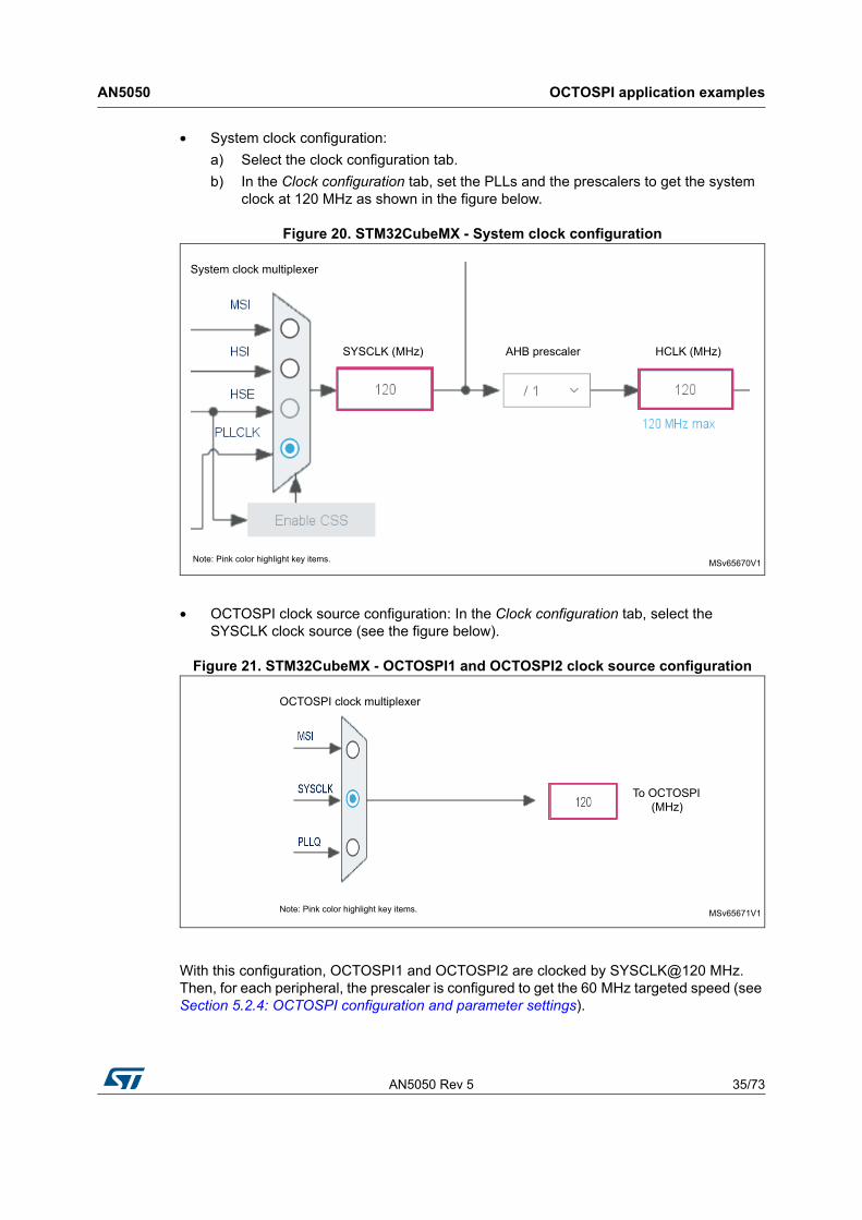
• System clock configuration:
a) Select the clock configuration tab.
b) In the Clock configuration tab, set the PLLs and the prescalers to get the system clock at 120 MHz as shown in the figure below.
Figure 20. STM32CubeMX - System clock configuration
• OCTOSPI clock source configuration: In the Clock configuration tab, select the SYSCLK clock source (see the figure below).
Figure 21. STM32CubeMX - OCTOSPI1 and OCTOSPI2 clock source configuration
With this configuration, OCTOSPI1 and OCTOSPI2 are clocked by SYSCLK@120 MHz. Then, for each peripheral, the prescaler is configured to get the 60 MHz targeted speed (see Section 5.2.4: OCTOSPI configuration and parameter settings).
MSv65670V1Note: Pink color highlight key items.
System clock multiplexer
AHB prescalerSYSCLK (MHz) HCLK (MHz)
MSv65671V1Note: Pink color highlight key items.
OCTOSPI clock multiplexer
To OCTOSPI (MHz)

OCTOSPI application examples AN5050
36/73 AN5050 Rev 5
5.2.4 OCTOSPI configuration and parameter settings
Once all of the OCTOSPI GPIOs and the clock configuration have been done, the user must configure the OCTOSPI depending on the used external memory and its communication protocol.

AN5050 Rev 5 37/73
AN5050 OCTOSPI application examples
72
1. In the OCTOSPI Configuration window, select the Parameter Settings tab as shown in the figure below and configure it by referencing to Table 5.
Figure 22. STM32CubeMx - OCTOSPI peripheral configuration window
2. Configure the OCTOSPI parameters depending on the memory used.
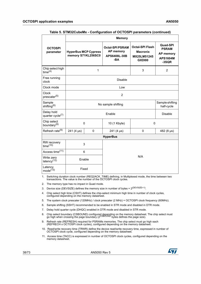
Table 5. STM32CubeMx - Configuration of OCTOSPI parameters
OCTOSPI parameter
Memory
HyperBus MCP Cypress memory S71KL256SC0
Octal-SPI PSRAM AP memory
APS6408L-30B-BA
Octal-SPI Flash
Macronix
MX25LM51245GXDI00
Quad-SPI PSRAM
AP memory
APS1604M-3SQR
Instance OCTOSPI1 OCTOSPI2 OCTOSPI1 OCTOSPI2 OCTOSPI1
Multiplexed
Switching duration clock number(1)
1 N/A
Generic
FIFO threshold 1
Dual mode Disable
Memory type HyperBus AP memory Macronix Micron(2)
Device size(3) 23
(8 Mbytes)
25
(128 Mbytes)
23
(8 Mbytes)
26
(256 Mbytes)
21
(2 Mbytes)
MSv65672V1Note: Pink color highlight key items.
OCTOSPI application examples AN5050
38/73 AN5050 Rev 5
Chip select high time(4) 1 3 2
Free running clock
Disable
Clock mode Low
Clock prescaler(5) 2
Sample shifting(6) No sample shifting
Sample shifting half-cycle
Delay hold quarter cycle(7) Enable Disable
Chip select boundary(8)
0 10 (1 Kbyte) 0
Refresh rate(9) 241 (4 μs) 0 241 (4 μs) 0 482 (8 μs)
HyperBus
RW recovery time(10) 3
N/A
Access time(11) 6
Write zero latency(12) Enable
Latency mode(13) Fixed
1. Switching duration clock number (REQ2ACK_TIME) defining, in Multiplexed mode, the time between two transactions. The value is the number of the OCTOSPI clock cycles.
2. The memory type has no impact in Quad mode.
3. Device size (DEVSIZE) defines the memory size in number of bytes = 2(DEVSIZE+1).
4. Chip select high time (CSHT) defines the chip-select minimum high time in number of clock cycles, configured depending on the memory datasheet.
5. The system clock prescaler (120MHz) / clock prescaler (2 MHz) = OCTOSPI clock frequency (60MHz).
6. Sample shifting (SSHT) recommended to be enabled in STR mode and disabled in DTR mode.
7. Delay hold quarter cycle (DHQC) enabled in DTR mode and disabled in STR mode.
8. Chip select boundary (CSBOUND) configured depending on the memory datasheet. The chip select must go high when crossing the page boundary (2CSBOUND bytes defines the page size).
9. Refresh rate (REFRESH) required for PSRAMs memories. The chip select must go high each (REFRECH x OCTOSPI clock cycles), configured depending on the memory datasheet.
10. Read/write recovery time (TRWR) define the device read/write recovery time, expressed in number of OCTOSPI clock cycle, configured depending on the memory datasheet.
11. Access time (TACC) is expressed in number of OCTOSPI clock cycles, configured depending on the memory datasheet.
Table 5. STM32CubeMx - Configuration of OCTOSPI parameters (continued)
OCTOSPI parameter
Memory
HyperBus MCP Cypress memory S71KL256SC0
Octal-SPI PSRAM AP memory
APS6408L-30B-BA
Octal-SPI Flash
Macronix
MX25LM51245GXDI00
Quad-SPI PSRAM
AP memory
APS1604M-3SQR
AN5050 Rev 5 39/73
AN5050 OCTOSPI application examples
72
3. Build and run the project: At this stage, the user can build, debug and run the project.
5.2.5 STM32CubeMX: Project generation
Once all of the GPIOs, the clock and the OCTOSPI configurations have been done, the user must generate the project with the desired toolchain (such as STM32CubeIDE, EWARM or MDK-ARM).
Indirect mode and Memory-mapped mode configuration
At this stage, the project must be already generated with GPIOs and OCTOSPI properly configured following the steps detailed in Section 5.2.3 andSection 5.2.4.
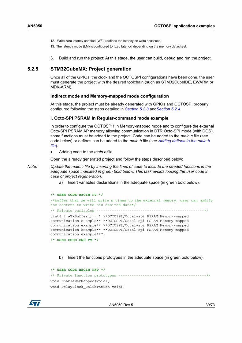
I. Octo-SPI PSRAM in Regular-command mode example
In order to configure the OCTOSPI1 in Memory-mapped mode and to configure the external Octo-SPI PSRAM AP memory allowing communication in DTR Octo-SPI mode (with DQS), some functions must be added to the project. Code can be added to the main.c file (see code below) or defines can be added to the main.h file (see Adding defines to the main.h file).
• Adding code to the main.c file
Open the already generated project and follow the steps described below:
Note: Update the main.c file by inserting the lines of code to include the needed functions in the adequate space indicated in green bold below. This task avoids loosing the user code in case of project regeneration.
a) Insert variables declarations in the adequate space (in green bold below).
/* USER CODE BEGIN PV */
/*buffer that we will write n times to the external memory, user can modify the content to write his desired data*/
/* Private variables -------------------------------------------------*/
uint8_t aTxBuffer[] = " **OCTOSPI/Octal-spi PSRAM Memory-mapped communication example** **OCTOSPI/Octal-spi PSRAM Memory-mapped communication example** **OCTOSPI/Octal-spi PSRAM Memory-mapped communication example** **OCTOSPI/Octal-spi PSRAM Memory-mapped communication example**";
/* USER CODE END PV */
b) Insert the functions prototypes in the adequate space (in green bold below).
/* USER CODE BEGIN PFP */
/* Private function prototypes ----------------------------------------*/
void EnableMemMapped(void);
void DelayBlock_Calibration(void);
12. Write zero latency enabled (WZL) defines the latency on write accesses.
13. The latency mode (LM) is configured to fixed latency, depending on the memory datasheet.

OCTOSPI application examples AN5050
40/73 AN5050 Rev 5
/* USER CODE END PFP */
c) Insert the functions to be called in the main() function, in the adequate space (in green bold below).
/* USER CODE BEGIN 1 */
__IO uint8_t *mem_addr;
uint32_t address = 0;
uint16_t index1;/*index1 counter of bytes used when reading/
writing 256 bytes buffer */
uint16_t index2;/*index2 counter of 256 bytes buffer used when reading/
writing the 1Mbytes extended buffer */
/* USER CODE END 1 */
/* USER CODE BEGIN 2 */
/*----------------------------------------------------------------------*/
/*Enable Memory Mapped Mode*/
EnableMemMapped();
/*----------------------------------------------------------------------*/
/*Enable the Delay Block Calibration*/
DelayBlock_Calibration();
/*----------------------------------------------------------------------*/
/* Writing Sequence of 1Mbyte */
mem_addr = (__IO uint8_t *)(OCTOSPI1_BASE + address);
/*Writing 1Mbyte (256Byte BUFFERSIZE x 4096 times) */
for (index2 = 0; index2 < EXTENDEDBUFFERSIZE/BUFFERSIZE; index2++)
{
for (index1 = 0; index1 < BUFFERSIZE; index1++)
{
*mem_addr = aTxBuffer[index1];
mem_addr++;
}
}
/*----------------------------------------------------------------------*/
/* Reading Sequence of 1Mbyte */
mem_addr = (__IO uint8_t *)(OCTOSPI1_BASE + address);
/*Reading 1Mbyte (256Byte BUFFERSIZE x 4096 times)*/
for (index2 = 0; index2 < EXTENDEDBUFFERSIZE/BUFFERSIZE; index2++) {
for (index1 = 0; index1 < BUFFERSIZE; index1++)
{
if (*mem_addr != aTxBuffer[index1])
{
/*if data read is corrupted we can toggle a led here: example blue led*/
}

AN5050 Rev 5 41/73
AN5050 OCTOSPI application examples
72
mem_addr++;
}
}
/*if data read is correct we can toggle a led here: example green led*/
/* USER CODE END 2 */
d) Insert the function definitions, called in the main(), in the adequate space (in green bold below).
/* USER CODE BEGIN 4 */
/*----------------------------------------------------------------------*/
/* This function enables memory-mapped mode for Read and Write operations */
void EnableMemMapped(void)
{
OSPI_RegularCmdTypeDef sCommand;
OSPI_MemoryMappedTypeDef sMemMappedCfg;
sCommand.FlashId = HAL_OSPI_FLASH_ID_1;
sCommand.InstructionMode = HAL_OSPI_INSTRUCTION_8_LINES;
sCommand.InstructionSize = HAL_OSPI_INSTRUCTION_8_BITS;
sCommand.InstructionDtrMode = HAL_OSPI_INSTRUCTION_DTR_DISABLE;
sCommand.AddressMode = HAL_OSPI_ADDRESS_8_LINES;
sCommand.AddressSize = HAL_OSPI_ADDRESS_32_BITS;
sCommand.AddressDtrMode = HAL_OSPI_ADDRESS_DTR_ENABLE;
sCommand.AlternateBytesMode = HAL_OSPI_ALTERNATE_BYTES_NONE;
sCommand.DataMode = HAL_OSPI_DATA_8_LINES;
sCommand.DataDtrMode = HAL_OSPI_DATA_DTR_ENABLE;
sCommand.DQSMode = HAL_OSPI_DQS_ENABLE;
sCommand.SIOOMode = HAL_OSPI_SIOO_INST_EVERY_CMD;
sCommand.Address = 0;
sCommand.NbData = 1;
/* Memory-mapped mode configuration for Linear burst write operations */
sCommand.OperationType = HAL_OSPI_OPTYPE_WRITE_CFG;
sCommand.Instruction = LINEAR_BURST_WRITE;
sCommand.DummyCycles = DUMMY_CLOCK_CYCLES_SRAM_WRITE;
if (HAL_OSPI_Command(&hospi1, &sCommand, HAL_OSPI_TIMEOUT_DEFAULT_VALUE) != HAL_OK)
{
Error_Handler();
}
/* Memory-mapped mode configuration for Linear burst read operations */
sCommand.OperationType = HAL_OSPI_OPTYPE_READ_CFG;
sCommand.Instruction = LINEAR_BURST_READ;
sCommand.DummyCycles = DUMMY_CLOCK_CYCLES_SRAM_READ;

OCTOSPI application examples AN5050
42/73 AN5050 Rev 5
if (HAL_OSPI_Command(&hospi1, &sCommand, HAL_OSPI_TIMEOUT_DEFAULT_VALUE) != HAL_OK)
{
Error_Handler();
}
/*Disable timeout counter for memory mapped mode*/
sMemMappedCfg.TimeOutActivation = HAL_OSPI_TIMEOUT_COUNTER_DISABLE;
/*Enable memory mapped mode*/
if (HAL_OSPI_MemoryMapped(&hospi1, &sMemMappedCfg) != HAL_OK)
{
Error_Handler();
}
}
/*----------------------------------------------------------------------*/
/*This function is used to calibrate the Delayblock before initiating USER's application read/write transactions*/
void DelayBlock_Calibration(void)
{
/*buffer used for calibration*/
uint8_t Cal_buffer[] = " ****Delay Block Calibration Buffer**** ****Delay Block Calibration Buffer**** ****Delay Block Calibration Buffer**** ****Delay Block Calibration Buffer**** ****Delay Block Calibration Buffer**** ****Delay Block Calibration Buffer**** ";
uint16_t index;
__IO uint8_t *mem_addr;
uint8_t test_failed;
uint8_t delay = 0x0;
uint8_t Min_found = 0;
uint8_t Max_found = 0;
uint8_t Min_Window = 0x0;
uint8_t Max_Window = 0xF;
uint8_t Mid_window = 0;
uint8_t calibration_ongoing = 1;
/* Write the Cal_buffer to the memory*/
mem_addr = (__IO uint8_t *)(OCTOSPI1_BASE);
for (index = 0; index < DLYB_BUFFERSIZE; index++)
{
*mem_addr = Cal_buffer[index];
mem_addr++;
}
while (calibration_ongoing)
{
/* update the Delayblock calibration */
HAL_RCCEx_OCTOSPIDelayConfig(delay, 0);
test_failed = 0;
mem_addr = (__IO uint8_t *)(OCTOSPI1_BASE);

AN5050 Rev 5 43/73
AN5050 OCTOSPI application examples
72
for (index = 0; index < DLYB_BUFFERSIZE; index++)
{
/* Read the Cal_buffer from the memory*/
if (*mem_addr != Cal_buffer[index])
{
/*incorrect data read*/
test_failed = 1;
}
mem_addr++;
}
/* search for the Min window */
if (Min_found!=1)
{
if (test_failed == 1)
{
if (delay < 15)
{
delay++;
}
else
{
/* If delay set to maximum and error still detected: can't use external PSRAM */
Error_Handler();
}
}
else
{
Min_Window = delay;
Min_found=1;
delay = 0xF;
}
}
/* search for the Max window */
else if (Max_found!=1)
{
if (test_failed == 1)
{
if (delay > 0)
{
delay--;
}
else
{

OCTOSPI application examples AN5050
44/73 AN5050 Rev 5
/* If delay set to minimum and error still detected: can't use external PSRAM */
Error_Handler();
}
}
else
{
Max_Window = delay;
Max_found=1;
}
}
/* min and max delay window found, configure the delay block with the middle window value and exit calibration */
else
{
Mid_window = (Max_Window+Min_Window)/2;
HAL_RCCEx_OCTOSPIDelayConfig(Mid_window, 0);
/* exit calibration */
calibration_ongoing = 0;
}
}
}
/* USER CODE END 4 */
• Adding defines to the main.h file
Update the main.h file by inserting the defines in the adequate space (in green bold below).
/* USER CODE BEGIN Private defines */
/*APS6408L-3OB PSRAM APmemory*/
#define LINEAR_BURST_READ 0x20
#define LINEAR_BURST_WRITE 0xA0
#define DUMMY_CLOCK_CYCLES_SRAM_READ 5
#define DUMMY_CLOCK_CYCLES_SRAM_WRITE 4
/* Exported macro -----------------------------------------------------*/
#define BUFFERSIZE (COUNTOF(aTxBuffer) - 1)
#define COUNTOF(__BUFFER__) (sizeof(__BUFFER__) / sizeof(*(__BUFFER__)))
#define DLYB_BUFFERSIZE (COUNTOF(Cal_buffer) - 1)
#define EXTENDEDBUFFERSIZE (1048576)
/* USER CODE END Private defines */
• Code is now ready, built and run.

AN5050 Rev 5 45/73
AN5050 OCTOSPI application examples
72
II. Octo-SPI FLASH in Regular-command mode example
In order to configure the OCTOSPI2 in Indirect/Memory-mapped mode and to configure the external Octo-SPI Macronix Flash memory allowing communication in DTR Octo-SPI mode (with DQS), some functions must be added to the project. Code can be added to the main.c file (see code below) or defines can be added to the main.h file (see Adding defines to the main.h file).
• Adding code to the main.c file
Open the already generated project and follow the steps described below:
Note: Update the main.c file by inserting the lines of code to include the needed functions in the adequate space indicated in green bold below. This task avoids loosing the user code in case of project regeneration.
a) Insert variables declarations in the adequate space (in green bold below).
/* USER CODE BEGIN PV */
/* Private variables --------------------------------------------------*/
uint8_t aTxBuffer[]=" Programming in indirect mode - Reading in memory-mapped mode ";
__IO uint8_t *nor_memaddr = (__IO uint8_t *)(OCTOSPI2_BASE);
__IO uint8_t aRxBuffer[BUFFERSIZE] ="";
/* USER CODE END PV */
b) Insert the functions prototypes in the adequate space (in green bold below).
/* USER CODE BEGIN PFP */
/* Private function prototypes ---------------------------------------*/
void WriteEnable(void);
void OctalWriteEnable(void);
void OctalDTR_MemoryCfg(void);
void OctalSectorErase(void);
void OctalDTR_MemoryWrite(void);
void AutoPollingWIP(void);
void OctalPollingWEL(void);
void OctalPollingWIP(void);
void EnableMemMapped(void);
/* USER CODE END PFP */
c) Insert the functions to be called in the main() function, in the adequate space (in green bold below).
/* USER CODE BEGIN 1 */
uint16_t index1;
/* USER CODE END 1 */

OCTOSPI application examples AN5050
46/73 AN5050 Rev 5
/* USER CODE BEGIN 2 */
/*----------------------------------------------------------------------*/
/*-------------- MX25LM51245G memory configuration --------------*/
/* Configure MX25LM51245G memory to DTR Octal I/O mode */
OctalDTR_MemoryCfg();
/*----------------------------------------------------------------------*/
/*----------------------- Erasing the first sector ----------------------*/
/* Enable writing to memory using Octal Write Enable cmd */
OctalWriteEnable();
/* Enable Octal Software Polling to wait until WEL=1 */
OctalPollingWEL ();
/* Erasing first sector using Octal erase cmd */
OctalSectorErase();
/* Enable Octal Software Polling to wait until memory is ready WIP=0*/
OctalPollingWIP();
/*----------------------------------------------------------------------*/
/*--------------------- Programming operation ----------------------*/
/* Enable writing to memory using Octal Write Enable cmd */
OctalWriteEnable();
/* Enable Octal Software Polling to wait until WEL=1 */
OctalPollingWEL();
/* Writing (using CPU) the aTxBuffer to the memory */
OctalDTR_MemoryWrite();
/* Enable Octal Software Polling to wait until memory is ready WIP=0*/
OctalPollingWIP();
/*---------------------------------------------------------------------*/
/*------ Configure memory-mapped Octal SDR Read/write ------*/
EnableMemMapped();
/*----------------------------------------------------------------------*/
/*---------------- Reading from the NOR memory ------------------*/
for(index = 0; index < BUFFERSIZE; index++)
{
/* Reading back the written aTxBuffer in memory-mapped mode */
aRxBuffer[index] = *nor_memaddr;
if(aRxBuffer[index] != aTxBuffer[index])
{
/* Can add code to toggle a LED when data doesn't match */
}
nor_memaddr++;
}
/*----------------------------------------------------------------------*/
/* USER CODE END 2 */

AN5050 Rev 5 47/73
AN5050 OCTOSPI application examples
72
d) Insert the function definitions, called in the main(), in the adequate space (in green bold below).
/* USER CODE BEGIN 4 */
/* This function Enables writing to the memory: write enable cmd is sent in single SPI mode */
void WriteEnable(void)
{
OSPI_RegularCmdTypeDef sCommand;
OSPI_AutoPollingTypeDef sConfig;
/* Initialize the Write Enable cmd in single SPI mode */
sCommand.OperationType = HAL_OSPI_OPTYPE_COMMON_CFG;
sCommand.FlashId = HAL_OSPI_FLASH_ID_1;
sCommand.Instruction = WRITE_ENABLE_CMD;
sCommand.InstructionMode = HAL_OSPI_INSTRUCTION_1_LINE;
sCommand.InstructionSize = HAL_OSPI_INSTRUCTION_8_BITS;
sCommand.InstructionDtrMode = HAL_OSPI_INSTRUCTION_DTR_DISABLE;
sCommand.AddressMode = HAL_OSPI_ADDRESS_NONE;
sCommand.AlternateBytesMode = HAL_OSPI_ALTERNATE_BYTES_NONE;
sCommand.DataMode = HAL_OSPI_DATA_NONE;
sCommand.DummyCycles = 0;
sCommand.DQSMode = HAL_OSPI_DQS_DISABLE;
sCommand.SIOOMode = HAL_OSPI_SIOO_INST_EVERY_CMD;
/* Send Write Enable command in single SPI mode */
if (HAL_OSPI_Command(&hospi2, &sCommand, HAL_OSPI_TIMEOUT_DEFAULT_VALUE) != HAL_OK)
{
Error_Handler();
}
/* Initialize Automatic-Polling mode to wait until WEL=1 */
sCommand.Instruction = READ_STATUS_REG_CMD;
sCommand.DataMode = HAL_OSPI_DATA_1_LINE;
sCommand.DataDtrMode = HAL_OSPI_DATA_DTR_DISABLE;
sCommand.NbData = 1;
if (HAL_OSPI_Command(&hospi2, &sCommand, HAL_OSPI_TIMEOUT_DEFAULT_VALUE) != HAL_OK)
{
Error_Handler();
}
/* Set the mask to 0x02 to mask all Status REG bits except WEL */
/* Set the match to 0x02 to check if the WEL bit is set */
sConfig.Match = WRITE_ENABLE_MATCH_VALUE;
sConfig.Mask = WRITE_ENABLE_MASK_VALUE;
sConfig.MatchMode = HAL_OSPI_MATCH_MODE_AND;
sConfig.Interval = AUTO_POLLING_INTERVAL;
sConfig.AutomaticStop = HAL_OSPI_AUTOMATIC_STOP_ENABLE;

OCTOSPI application examples AN5050
48/73 AN5050 Rev 5
/* Start Automatic-Polling mode to wait until WEL=1 */
if (HAL_OSPI_AutoPolling(&hospi2, &sConfig, HAL_OSPI_TIMEOUT_DEFAULT_VALUE) != HAL_OK)
{
Error_Handler();
}
}
/* This functions Enables writing to the memory: write enable cmd is sent in Octal SPI mode */
void OctalWriteEnable(void)
{
OSPI_RegularCmdTypeDef sCommand;
/* Initialize the Write Enable cmd */
sCommand.OperationType = HAL_OSPI_OPTYPE_COMMON_CFG;
sCommand.FlashId = HAL_OSPI_FLASH_ID_1;
sCommand.Instruction = OCTAL_WRITE_ENABLE_CMD;
sCommand.InstructionMode = HAL_OSPI_INSTRUCTION_8_LINES;
sCommand.InstructionSize = HAL_OSPI_INSTRUCTION_16_BITS;
sCommand.InstructionDtrMode = HAL_OSPI_INSTRUCTION_DTR_ENABLE;
sCommand.AddressMode = HAL_OSPI_ADDRESS_NONE;
sCommand.AlternateBytesMode = HAL_OSPI_ALTERNATE_BYTES_NONE;
sCommand.DataMode = HAL_OSPI_DATA_NONE;
sCommand.DummyCycles = 0;
sCommand.DQSMode = HAL_OSPI_DQS_DISABLE;
sCommand.SIOOMode = HAL_OSPI_SIOO_INST_EVERY_CMD;
/* Send Write Enable command in Octal mode */
if (HAL_OSPI_Command(&hospi2, &sCommand, HAL_OSPI_TIMEOUT_DEFAULT_VALUE) != HAL_OK)
{
Error_Handler();
}
}
/* This function Configures Software polling to wait until WEL=1 */
void OctalPollingWEL(void)
{
OSPI_AutoPollingTypeDef sConfig;
OSPI_RegularCmdTypeDef sCommand;
/* Initialize Indirect read mode for Software Polling to wait until WEL=1 */
sCommand.OperationType = HAL_OSPI_OPTYPE_COMMON_CFG;
sCommand.FlashId = HAL_OSPI_FLASH_ID_1;
sCommand.Instruction = OCTAL_READ_STATUS_REG;
sCommand.InstructionMode = HAL_OSPI_INSTRUCTION_8_LINES;
sCommand.InstructionSize = HAL_OSPI_INSTRUCTION_16_BITS;
sCommand.InstructionDtrMode = HAL_OSPI_INSTRUCTION_DTR_ENABLE;
sCommand.Address = 0x0;
sCommand.AddressMode = HAL_OSPI_ADDRESS_8_LINES;

AN5050 Rev 5 49/73
AN5050 OCTOSPI application examples
72
sCommand.AddressSize = HAL_OSPI_ADDRESS_32_BITS;
sCommand.AddressDtrMode = HAL_OSPI_ADDRESS_DTR_ENABLE;
sCommand.AlternateBytesMode = HAL_OSPI_ALTERNATE_BYTES_NONE;
sCommand.DataMode = HAL_OSPI_DATA_8_LINES;
sCommand.DataDtrMode = HAL_OSPI_DATA_DTR_ENABLE;
sCommand.NbData = 2;
sCommand.DummyCycles = DUMMY_CLOCK_CYCLES_READ_REG;
sCommand.DQSMode = HAL_OSPI_DQS_DISABLE;
sCommand.SIOOMode = HAL_OSPI_SIOO_INST_EVERY_CMD;
/* Set the mask to 0x02 to mask all Status REG bits except WEL */
/* Set the match to 0x02 to check if the WEL bit is Set */
sConfig.Match = WRITE_ENABLE_MATCH_VALUE;
sConfig.Mask = WRITE_ENABLE_MASK_VALUE;
sConfig.MatchMode = HAL_OSPI_MATCH_MODE_AND;
sConfig.Interval = 0x10;
sConfig.AutomaticStop = HAL_OSPI_AUTOMATIC_STOP_ENABLE;
if (HAL_OSPI_Command(&hospi2, &sCommand, HAL_OSPI_TIMEOUT_DEFAULT_VALUE) != HAL_OK)
{
Error_Handler();
}
/* Start Automatic-Polling mode to wait until the memory is ready WEL=1 */
if (HAL_OSPI_AutoPolling(&hospi2, &sConfig, HAL_OSPI_TIMEOUT_DEFAULT_VALUE) != HAL_OK)
{
Error_Handler();
}
}
/* This function Configures Automatic-polling mode to wait until WIP=0 */
void AutoPollingWIP(void)
{
OSPI_RegularCmdTypeDef sCommand;
OSPI_AutoPollingTypeDef sConfig;
/* Initialize Automatic-Polling mode to wait until WIP=0 */
sCommand.OperationType = HAL_OSPI_OPTYPE_COMMON_CFG;
sCommand.FlashId = HAL_OSPI_FLASH_ID_1;
sCommand.Instruction = READ_STATUS_REG_CMD;
sCommand.InstructionMode = HAL_OSPI_INSTRUCTION_1_LINE;
sCommand.InstructionSize = HAL_OSPI_INSTRUCTION_8_BITS;
sCommand.InstructionDtrMode = HAL_OSPI_INSTRUCTION_DTR_DISABLE;
sCommand.AddressMode = HAL_OSPI_ADDRESS_NONE;
sCommand.AlternateBytesMode = HAL_OSPI_ALTERNATE_BYTES_NONE;
sCommand.DummyCycles = 0;
sCommand.DQSMode = HAL_OSPI_DQS_DISABLE;

OCTOSPI application examples AN5050
50/73 AN5050 Rev 5
sCommand.SIOOMode = HAL_OSPI_SIOO_INST_EVERY_CMD;
sCommand.DataMode = HAL_OSPI_DATA_1_LINE;
sCommand.NbData = 1;
sCommand.DataDtrMode = HAL_OSPI_DATA_DTR_DISABLE;
/* Set the mask to 0x01 to mask all Status REG bits except WIP */
/* Set the match to 0x00 to check if the WIP bit is Reset */
sConfig.Match = MEMORY_READY_MATCH_VALUE;
sConfig.Mask = MEMORY_READY_MASK_VALUE;
sConfig.MatchMode = HAL_OSPI_MATCH_MODE_AND;
sConfig.Interval = 0x10;
sConfig.AutomaticStop = HAL_OSPI_AUTOMATIC_STOP_ENABLE;
if (HAL_OSPI_Command(&hospi2, &sCommand, HAL_OSPI_TIMEOUT_DEFAULT_VALUE) != HAL_OK)
{
Error_Handler();
}
/* Start Automatic-Polling mode to wait until the memory is ready WIP=0 */
if (HAL_OSPI_AutoPolling(&hospi2, &sConfig, HAL_OSPI_TIMEOUT_DEFAULT_VALUE) != HAL_OK)
{
Error_Handler();
}
}
/* This function Configures Software polling mode to wait the memory is ready WIP=0 */
void OctalPollingWIP(void)
{
OSPI_RegularCmdTypeDef sCommand;
OSPI_AutoPollingTypeDef sConfig;
/* Initialize Automatic-Polling mode to wait until WIP=0 */
sCommand.OperationType = HAL_OSPI_OPTYPE_COMMON_CFG;
sCommand.FlashId = HAL_OSPI_FLASH_ID_1;
sCommand.Instruction = OCTAL_READ_STATUS_REG;
sCommand.InstructionMode = HAL_OSPI_INSTRUCTION_8_LINES;
sCommand.InstructionSize = HAL_OSPI_INSTRUCTION_16_BITS;
sCommand.InstructionDtrMode = HAL_OSPI_INSTRUCTION_DTR_ENABLE;
sCommand.Address = 0x0;
sCommand.AddressMode = HAL_OSPI_ADDRESS_8_LINES;
sCommand.AddressSize = HAL_OSPI_ADDRESS_32_BITS;
sCommand.AddressDtrMode = HAL_OSPI_ADDRESS_DTR_ENABLE;
sCommand.AlternateBytesMode = HAL_OSPI_ALTERNATE_BYTES_NONE;
sCommand.DataMode = HAL_OSPI_DATA_8_LINES;
sCommand.DataDtrMode = HAL_OSPI_DATA_DTR_ENABLE;
sCommand.NbData = 2;
sCommand.DummyCycles = DUMMY_CLOCK_CYCLES_READ_REG;

AN5050 Rev 5 51/73
AN5050 OCTOSPI application examples
72
sCommand.DQSMode = HAL_OSPI_DQS_DISABLE;
sCommand.SIOOMode = HAL_OSPI_SIOO_INST_EVERY_CMD;
/* Set the mask to 0x01 to mask all Status REG bits except WIP */
/* Set the match to 0x00 to check if the WIP bit is Reset */
sConfig.Match = MEMORY_READY_MATCH_VALUE;
sConfig.Mask = MEMORY_READY_MASK_VALUE;
sConfig.MatchMode = HAL_OSPI_MATCH_MODE_AND;
sConfig.Interval = 0x10;
sConfig.AutomaticStop = HAL_OSPI_AUTOMATIC_STOP_ENABLE;
if (HAL_OSPI_Command(&hospi2, &sCommand, HAL_OSPI_TIMEOUT_DEFAULT_VALUE) != HAL_OK)
{
Error_Handler();
}
/* Start Automatic-Polling mode to wait until the memory is ready WIP=0 */
if (HAL_OSPI_AutoPolling(&hospi2, &sConfig, HAL_OSPI_TIMEOUT_DEFAULT_VALUE) != HAL_OK)
{
Error_Handler();
}
}
/*** This function configures the MX25LM51245G memory ***/
void OctalDTR_MemoryCfg(void)
{
OSPI_RegularCmdTypeDef sCommand;
uint8_t tmp;
/* Enable writing to memory in order to set Dummy */
WriteEnable();
/* Initialize Indirect write mode to configure Dummy */
sCommand.OperationType = HAL_OSPI_OPTYPE_COMMON_CFG;
sCommand.FlashId = HAL_OSPI_FLASH_ID_1;
sCommand.InstructionMode = HAL_OSPI_INSTRUCTION_1_LINE;
sCommand.InstructionSize = HAL_OSPI_INSTRUCTION_8_BITS;
sCommand.InstructionDtrMode = HAL_OSPI_INSTRUCTION_DTR_DISABLE;
sCommand.Instruction = WRITE_CFG_REG_2_CMD;
sCommand.Address = CONFIG_REG2_ADDR3;
sCommand.AddressMode = HAL_OSPI_ADDRESS_1_LINE;
sCommand.AddressSize = HAL_OSPI_ADDRESS_32_BITS;
sCommand.AddressDtrMode = HAL_OSPI_ADDRESS_DTR_DISABLE;
sCommand.AlternateBytesMode = HAL_OSPI_ALTERNATE_BYTES_NONE;
sCommand.DataMode = HAL_OSPI_DATA_1_LINE;
sCommand.DataDtrMode= HAL_OSPI_DATA_DTR_DISABLE;
sCommand.NbData = 1;
sCommand.DummyCycles = 0;
sCommand.DQSMode = HAL_OSPI_DQS_DISABLE;

OCTOSPI application examples AN5050
52/73 AN5050 Rev 5
sCommand.SIOOMode = HAL_OSPI_SIOO_INST_EVERY_CMD;
if (HAL_OSPI_Command(&hospi2, &sCommand, HAL_OSPI_TIMEOUT_DEFAULT_VALUE) != HAL_OK)
{
Error_Handler();
}
/* Write Configuration register 2 with new dummy cycles */
tmp = CR2_DUMMY_CYCLES_66MHZ;
if (HAL_OSPI_Transmit(&hospi2, &tmp, HAL_OSPI_TIMEOUT_DEFAULT_VALUE) != HAL_OK)
{
Error_Handler();
}
AutoPollingWIP();
/* Enable writing to memory in order to set Octal DTR mode */
WriteEnable();
/* Initialize OCTOSPI1 to Indirect write mode to configure Octal mode */
sCommand.Instruction = WRITE_CFG_REG_2_CMD;
sCommand.Address = CONFIG_REG2_ADDR1;
sCommand.AddressMode = HAL_OSPI_ADDRESS_1_LINE;
if (HAL_OSPI_Command(&hospi2, &sCommand, HAL_OSPI_TIMEOUT_DEFAULT_VALUE) != HAL_OK)
{
Error_Handler();
}
/* Write Configuration register 2 with with Octal mode */
tmp = CR2_DTR_OPI_ENABLE;
if (HAL_OSPI_Transmit(&hospi2, &tmp, HAL_OSPI_TIMEOUT_DEFAULT_VALUE) != HAL_OK)
{
Error_Handler();
}
}
/* This function erases the first memory sector */
void OctalSectorErase(void)
{
OSPI_RegularCmdTypeDef sCommand;
/* Initialize Indirect write mode to erase the first sector */
sCommand.OperationType = HAL_OSPI_OPTYPE_COMMON_CFG;
sCommand.FlashId = HAL_OSPI_FLASH_ID_1;
sCommand.Instruction = OCTAL_SECTOR_ERASE_CMD;
sCommand.InstructionMode = HAL_OSPI_INSTRUCTION_8_LINES;
sCommand.InstructionSize = HAL_OSPI_INSTRUCTION_16_BITS;
sCommand.InstructionDtrMode = HAL_OSPI_INSTRUCTION_DTR_ENABLE;
sCommand.AlternateBytesMode = HAL_OSPI_ALTERNATE_BYTES_NONE;
sCommand.DataMode = HAL_OSPI_DATA_NONE;

AN5050 Rev 5 53/73
AN5050 OCTOSPI application examples
72
sCommand.DataDtrMode = HAL_OSPI_DATA_DTR_ENABLE;
sCommand.DummyCycles = 0;
sCommand.DQSMode = HAL_OSPI_DQS_DISABLE;
sCommand.SIOOMode = HAL_OSPI_SIOO_INST_EVERY_CMD;
sCommand.AddressDtrMode = HAL_OSPI_ADDRESS_DTR_ENABLE;
sCommand.AddressMode = HAL_OSPI_ADDRESS_8_LINES;
sCommand.AddressSize = HAL_OSPI_ADDRESS_32_BITS;
sCommand.Address = 0;
/* Send Octal Sector erase cmd */
if (HAL_OSPI_Command(&hospi2, &sCommand, HAL_OSPI_TIMEOUT_DEFAULT_VALUE) != HAL_OK)
{
Error_Handler();
}
}
/* This function writes the memory */
void OctalDTR_MemoryWrite(void)
{
OSPI_RegularCmdTypeDef sCommand;
/* Initialize Indirect write mode for memory programming */
sCommand.OperationType = HAL_OSPI_OPTYPE_COMMON_CFG;
sCommand.FlashId = HAL_OSPI_FLASH_ID_1;
sCommand.Instruction = OCTAL_PAGE_PROG_CMD;
sCommand.InstructionMode = HAL_OSPI_INSTRUCTION_8_LINES;
sCommand.InstructionSize = HAL_OSPI_INSTRUCTION_16_BITS;
sCommand.AddressMode = HAL_OSPI_ADDRESS_8_LINES;
sCommand.AddressSize = HAL_OSPI_ADDRESS_32_BITS;
sCommand.Address = 0x00000000;
sCommand.AlternateBytesMode = HAL_OSPI_ALTERNATE_BYTES_NONE;
sCommand.DataMode = HAL_OSPI_DATA_8_LINES;
sCommand.NbData = BUFFERSIZE;
sCommand.DummyCycles = 0;
sCommand.SIOOMode = HAL_OSPI_SIOO_INST_EVERY_CMD;
sCommand.InstructionDtrMode = HAL_OSPI_INSTRUCTION_DTR_ENABLE;
sCommand.AddressDtrMode = HAL_OSPI_ADDRESS_DTR_ENABLE;
sCommand.DataDtrMode = HAL_OSPI_DATA_DTR_ENABLE;
sCommand.DQSMode = HAL_OSPI_DQS_ENABLE;
if (HAL_OSPI_Command(&hospi2, &sCommand, HAL_OSPI_TIMEOUT_DEFAULT_VALUE) != HAL_OK)
{
Error_Handler();
}
/* Memory Page programming */
if (HAL_OSPI_Transmit(&hospi2, aTxBuffer, HAL_OSPI_TIMEOUT_DEFAULT_VALUE)!= HAL_OK)
{

OCTOSPI application examples AN5050
54/73 AN5050 Rev 5
Error_Handler();
}
}
/* This function enables memory-mapped mode for Read and Write */
void EnableMemMapped(void)
{ OSPI_RegularCmdTypeDef sCommand;
OSPI_MemoryMappedTypeDef sMemMappedCfg;
/* Initialize memory-mapped mode for read operations */
sCommand.OperationType = HAL_OSPI_OPTYPE_READ_CFG;
sCommand.FlashId = HAL_OSPI_FLASH_ID_1;
sCommand.InstructionMode = HAL_OSPI_INSTRUCTION_8_LINES;
sCommand.InstructionSize = HAL_OSPI_INSTRUCTION_16_BITS;
sCommand.AddressMode = HAL_OSPI_ADDRESS_8_LINES;
sCommand.AddressSize = HAL_OSPI_ADDRESS_32_BITS;
sCommand.AlternateBytesMode = HAL_OSPI_ALTERNATE_BYTES_NONE;
sCommand.DataMode = HAL_OSPI_DATA_8_LINES;
sCommand.DummyCycles = DUMMY_CLOCK_CYCLES_READ;
sCommand.SIOOMode = HAL_OSPI_SIOO_INST_EVERY_CMD;
sCommand.Instruction = OCTAL_IO_DTR_READ_CMD;
sCommand.InstructionDtrMode = HAL_OSPI_INSTRUCTION_DTR_ENABLE;
sCommand.AddressDtrMode = HAL_OSPI_ADDRESS_DTR_ENABLE;
sCommand.DataDtrMode = HAL_OSPI_DATA_DTR_ENABLE;
sCommand.DQSMode = HAL_OSPI_DQS_ENABLE;
if (HAL_OSPI_Command(&hospi2, &sCommand, HAL_OSPI_TIMEOUT_DEFAULT_VALUE) != HAL_OK)
{
Error_Handler();
}
/* Initialize memory-mapped mode for write operations */
sCommand.OperationType = HAL_OSPI_OPTYPE_WRITE_CFG;
sCommand.Instruction = OCTAL_PAGE_PROG_CMD;
sCommand.DummyCycles = 0;
if (HAL_OSPI_Command(&hospi2, &sCommand, HAL_OSPI_TIMEOUT_DEFAULT_VALUE) != HAL_OK)
{
Error_Handler();
}
/* Configure the memory mapped mode with TimeoutCounter Disabled*/
sMemMappedCfg.TimeOutActivation = HAL_OSPI_TIMEOUT_COUNTER_DISABLE;
if (HAL_OSPI_MemoryMapped(&hospi2, &sMemMappedCfg) != HAL_OK)
{
Error_Handler();
}
}
/* USER CODE END 4 */

AN5050 Rev 5 55/73
AN5050 OCTOSPI application examples
72
• Adding defines to the main.h file
Update the main.h file by inserting the defines in the adequate space (in green bold below).
/* USER CODE BEGIN Private defines */
/* MX25LM512ABA1G12 Macronix memory */
/* Flash commands */
#define OCTAL_IO_DTR_READ_CMD 0xEE11
#define OCTAL_IO_READ_CMD 0xEC13
#define OCTAL_PAGE_PROG_CMD 0x12ED
#define OCTAL_READ_STATUS_REG_CMD 0x05FA
#define OCTAL_SECTOR_ERASE_CMD 0x21DE
#define OCTAL_WRITE_ENABLE_CMD 0x06F9
#define READ_STATUS_REG_CMD 0x05
#define WRITE_CFG_REG_2_CMD 0x72
#define WRITE_ENABLE_CMD 0x06
/* Dummy clocks cycles */
#define DUMMY_CLOCK_CYCLES_READ 6
#define DUMMY_CLOCK_CYCLES_READ_REG 4
/* Auto-polling values */
#define WRITE_ENABLE_MATCH_VALUE 0x02
#define WRITE_ENABLE_MASK_VALUE 0x02
#define MEMORY_READY_MATCH_VALUE 0x00
#define MEMORY_READY_MASK_VALUE 0x01
#define AUTO_POLLING_INTERVAL 0x10
/* Memory registers address */
#define CONFIG_REG2_ADDR1 0x0000000
#define CR2_STR_OPI_ENABLE 0x01
#define CR2_DTR_OPI_ENABLE 0x02
#define CONFIG_REG2_ADDR3 0x00000300
#define CR2_DUMMY_CYCLES_66MHZ 0x07
/* Exported macro ------------------------------------------------------*/
#define COUNTOF(__BUFFER__) (sizeof(__BUFFER__)/sizeof(*(__BUFFER__)))
/* Size of buffers */
#define BUFFERSIZE (COUNTOF(aTxBuffer) - 1)
/* USER CODE END Private defines */
• Code is now ready, built and run.

OCTOSPI application examples AN5050
56/73 AN5050 Rev 5
III. Quad-SPI PSRAM in Regular-command mode example
In order to configure the OCTOSPI1 in Indirect/Memory-mapped mode and to configure the external Quad-SPI PSRAM AP memory allowing communication in STR Quad-SPI mode, some functions must be added to the project. Code can be added to the main.c file (see code below) or defines can be added to the main.h file (see Adding defines to the main.h file).
• Adding code to the main.c file
Open the already generated project and follow the steps described below:
Note: Update the main.c file by inserting the lines of code to include the needed functions in the adequate space indicated in green bold below. This task avoids loosing the user code in case of project regeneration.
a) Insert variables declarations in the adequate space (in green bold below).
/* USER CODE BEGIN PV */
/*buffer that we will write n times to the external memory , user can modify the content to write his desired data */
uint8_t aTxBuffer[] = " **OCTOSPI/Quad-spi PSRAM Memory-mapped communication example** **OCTOSPI/Quad-spi PSRAM Memory-mapped communication example** **OCTOSPI/Quad-spi PSRAM Memory-mapped communication example** **OCTOSPI/Quad-spi PSRAM Memory-mapped communication example** ";
/* USER CODE END PV */
b) Insert the functions prototypes in the adequate space (in green bold below).
/* USER CODE BEGIN PFP */
void EnterQuadMode(void);
void EnableMemMappedQuadMode(void);
/* USER CODE END PFP */
c) Insert the functions to be called in the main() function, in the adequate space (in green bold below).
/* USER CODE BEGIN 1 */
__IO uint8_t *mem_addr;
uint32_t address = 0;
uint16_t index1; /*index1 counter of bytes used when reading/writing 256 bytes buffer */
uint16_t index2; /*index2 counter of 256 bytes buffer used when reading/writing the 1Mbytes extended buffer */
/* USER CODE END 1 */

AN5050 Rev 5 57/73
AN5050 OCTOSPI application examples
72
/* USER CODE BEGIN 2 */
/* Enter Quad Mode 4-4-4 --------------------------------------------- */
EnterQuadMode();
/* Enable Memory mapped in Quad mode -------------------------------- */
EnableMemMappedQuadMode();
/* Writing Sequence of 1Mbyte --------------------------------------- */
mem_addr = (__IO uint8_t *)(OCTOSPI1_BASE + address);
for (index2 = 0; index2 < EXTENDEDBUFFERSIZE/BUFFERSIZE; index2++)
/*Writing 1Mbyte (256Byte BUFFERSIZE x 4096 times) */
{
for (index1 = 0; index1 < BUFFERSIZE; index1++)
{
*mem_addr = aTxBuffer[index1];
mem_addr++;
}
}
/* Reading Sequence of 1Mbyte ---------------------------------------- */
mem_addr = (__IO uint8_t *)(OCTOSPI1_BASE + address);
for (index2 = 0; index2 < EXTENDEDBUFFERSIZE/BUFFERSIZE; index2++)
/*Reading 1Mbyte (256Byte BUFFERSIZE x 4096 times)*/
{
for (index1 = 0; index1 < BUFFERSIZE; index1++)
{
if (*mem_addr != aTxBuffer[index1])
{
/*can toggle led here*/
}
mem_addr++;
}
}
/*can toggle led here*/
/* USER CODE END 2 */

OCTOSPI application examples AN5050
58/73 AN5050 Rev 5
d) Insert the function definitions, called in the main(), in the adequate space (in green bold below).
/* USER CODE BEGIN 4 */
/*Function to Enable Memory mapped mode in Quad mode 4-4-4*/
void EnableMemMappedQuadMode(void)
{
OSPI_RegularCmdTypeDef sCommand;
OSPI_MemoryMappedTypeDef sMemMappedCfg;
sCommand.FlashId = HAL_OSPI_FLASH_ID_1;
sCommand.InstructionMode = HAL_OSPI_INSTRUCTION_4_LINES;
sCommand.InstructionSize = HAL_OSPI_INSTRUCTION_8_BITS;
sCommand.InstructionDtrMode = HAL_OSPI_INSTRUCTION_DTR_DISABLE;
sCommand.AddressMode = HAL_OSPI_ADDRESS_4_LINES;
sCommand.AddressSize = HAL_OSPI_ADDRESS_24_BITS;
sCommand.AddressDtrMode = HAL_OSPI_ADDRESS_DTR_DISABLE;
sCommand.AlternateBytesMode = HAL_OSPI_ALTERNATE_BYTES_NONE;
sCommand.DataMode = HAL_OSPI_DATA_4_LINES;
sCommand.DataDtrMode = HAL_OSPI_DATA_DTR_DISABLE;
sCommand.SIOOMode = HAL_OSPI_SIOO_INST_EVERY_CMD;
sCommand.Address = 0;
sCommand.NbData = 1;
/* Memory-mapped mode configuration for Quad Read mode 4-4-4*/
sCommand.OperationType = HAL_OSPI_OPTYPE_READ_CFG;
sCommand.Instruction = FAST_READ_QUAD;
sCommand.DummyCycles = FAST_READ_QUAD_DUMMY_CYCLES;
if (HAL_OSPI_Command(&hospi1, &sCommand, HAL_OSPI_TIMEOUT_DEFAULT_VALUE) != HAL_OK)
{
Error_Handler();
}
/* Memory-mapped mode configuration for Quad Write mode 4-4-4*/
sCommand.OperationType = HAL_OSPI_OPTYPE_WRITE_CFG;
sCommand.Instruction = QUAD_WRITE;
sCommand.DummyCycles = WRITE_QUAD_DUMMY_CYCLES;
sCommand.DQSMode = HAL_OSPI_DQS_ENABLE;
if (HAL_OSPI_Command(&hospi1, &sCommand, HAL_OSPI_TIMEOUT_DEFAULT_VALUE) != HAL_OK)
{
Error_Handler();
}
/*Disable timeout counter for memory mapped mode*/
sMemMappedCfg.TimeOutActivation = HAL_OSPI_TIMEOUT_COUNTER_DISABLE;
/*Enable memory mapped mode*/

AN5050 Rev 5 59/73
AN5050 OCTOSPI application examples
72
if (HAL_OSPI_MemoryMapped(&hospi1, &sMemMappedCfg) != HAL_OK)
{
Error_Handler();
}
}
/*Function to configure the external memory in Quad mode 4-4-4*/
void EnterQuadMode(void)
{
OSPI_RegularCmdTypeDef sCommand;
sCommand.OperationType = HAL_OSPI_OPTYPE_COMMON_CFG;
sCommand.FlashId = HAL_OSPI_FLASH_ID_1;
sCommand.Instruction = ENTER_QUAD_MODE;
sCommand.InstructionMode = HAL_OSPI_INSTRUCTION_1_LINE;
sCommand.InstructionSize = HAL_OSPI_INSTRUCTION_8_BITS;
sCommand.InstructionDtrMode = HAL_OSPI_INSTRUCTION_DTR_DISABLE;
sCommand.AddressMode = HAL_OSPI_ADDRESS_NONE;
sCommand.AlternateBytesMode = HAL_OSPI_ALTERNATE_BYTES_NONE;
sCommand.DataMode = HAL_OSPI_DATA_NONE;
sCommand.DummyCycles = ENTER_QUAD_DUMMY_CYCLES;
sCommand.DQSMode = HAL_OSPI_DQS_DISABLE;
sCommand.SIOOMode = HAL_OSPI_SIOO_INST_EVERY_CMD;
/*Enter QUAD mode*/
if (HAL_OSPI_Command(&hospi1, &sCommand, HAL_OSPI_TIMEOUT_DEFAULT_VALUE) != HAL_OK)
{
Error_Handler();
}
}
/* USER CODE END 4 */

OCTOSPI application examples AN5050
60/73 AN5050 Rev 5
• Adding defines to the main.h file
Update the main.h file by inserting the defines in the adequate space (in green bold below).
/* USER CODE BEGIN Private defines */
/*APS1604M-3SQR PSRAM APmemory*/
#define FAST_READ_QUAD 0xEB
#define QUAD_WRITE 0x38
#define FAST_READ_QUAD_DUMMY_CYCLES 6
#define WRITE_QUAD_DUMMY_CYCLES 0
#define ENTER_QUAD_DUMMY_CYCLES 0
#define QUAD_WRITE 0x38
#define ENTER_QUAD_MODE 0x35
#define EXIT_QUAD_MODE 0xF5
/* Exported macro -----------------------------------------------------*/
#define BUFFERSIZE (COUNTOF(aTxBuffer) - 1)
#define COUNTOF(__BUFFER__) (sizeof(__BUFFER__) / sizeof(*(__BUFFER__)))
#define EXTENDEDBUFFERSIZE (1048576)
/* USER CODE END Private defines */
• Code is now ready, built and run.

AN5050 Rev 5 61/73
AN5050 OCTOSPI application examples
72
IV. HyperFlash and HyperRAM memories with Multiplexed mode example
The following example shows how to read data from the external HyperFlash using DMA1, while the CPU reads data from the HyperRAM.
The DMA1 must be configured using the STM32CubeMx, with the following steps under system core:
• Select DMA.
• Under MemToMem, select Add.
• Configure the DMA request and the DMA request settings like the figure below.
Figure 23. STM32CubeMx - DMA1 configuration
In order to configure the OCTOSPI1 and OCTOSPI2 in Memory-mapped mode and to read data from the two external HyperBus memories, some functions must be added to the project. Code can be added to the main.c file (see code below) or defines can be added to the main.h file (see Adding defines to the main.h file).
• Adding code to the main.c file
Open the already generated project and follow the steps described below:
Note: Update the main.c file by inserting the lines of code to include the needed functions in the adequate space indicated in green bold below. This task avoids loosing the user code in case of project regeneration.
a) Insert variables declarations in the adequate space (in green bold below).
/* USER CODE BEGIN PV */
/*define a 64Kbyte buffer for HyperRam data read with CPU*/
#pragma location = 0x20020000
uint32_t RxHyperRAM[BUFFERSIZE];
/* USER CODE END PV */
MSv65673V1Note: Pink color highlight key items.

OCTOSPI application examples AN5050
62/73 AN5050 Rev 5
b) Insert the functions prototypes in the adequate space (in green bold below).
/* USER CODE BEGIN PFP */
void EnableMemMapped(void);
void DelayBlock_Calibration(void);
/* USER CODE END PFP */
c) Insert the functions to be called in the main() function, in the adequate space (in green bold below).
/* USER CODE BEGIN 1 */
/*pointer on OCTOSPI1 memory mapped address region*/
__IO uint32_t *OCTOSPI1_MEMMAPPED_ADD = (__IO uint32_t *)(OCTOSPI1_BASE);
/* USER CODE END 1 */
/* USER CODE BEGIN 2 */
/*Configure the MAXTRAN feature for 241 clock cycles for OCTOSPI1 and OCTOSPI2 (4µs of max transaction period)*/
MAXTRAN_Configuration();
/*Configure and Enable the Memory Mapped mode for both OCTOSPI1 and OCTOSPI2 respectively at address 0x90000000 and 0x70000000*/
EnableMemMapped();
/*Delay block Calibration*/
DelayBlock_Calibration();
/*Start Data read (64Kbyte) with DMA1 from the HyperFlash (0x70000000) to the internal SRAM3 (0x20030000)*/
if(HAL_DMA_Start(&hdma_memtomem_dma1_channel1,OCTOSPI2_BASE, SRAM3_BASE, BUFFERSIZE) != HAL_OK)
{
Error_Handler();
}
/*Start Data read (64Kbyte) with CPU from the HyperRAM (0x90000000) to
the internal SRAM2 (0x20020000) while the DMA is reading from HyperFLASH*/
for (index = 0; index < BUFFERSIZE; index++)
{
RxHyperRAM[index] = *OCTOSPI1_MEMMAPPED_ADD++;
}
/* USER CODE END 2 */

AN5050 Rev 5 63/73
AN5050 OCTOSPI application examples
72
d) Insert the function definitions, called in the main(), in the adequate space (in green bold below).
/* USER CODE BEGIN 4 */
/* Memory-mapped mode configuration for OCTOSPI1 and OCTOSPI2--------- */
void EnableMemMapped(void)
{
OSPI_HyperbusCmdTypeDef sCommand;
OSPI_MemoryMappedTypeDef sMemMappedCfg;
/* Memory-mapped mode configuration ---------------------------------- */
sCommand.AddressSpace = HAL_OSPI_MEMORY_ADDRESS_SPACE;
sCommand.AddressSize = HAL_OSPI_ADDRESS_32_BITS;
sCommand.DQSMode = HAL_OSPI_DQS_ENABLE;
sCommand.Address = 0;
sCommand.NbData = 1;
if (HAL_OSPI_HyperbusCmd(&hospi1, &sCommand, HAL_OSPI_TIMEOUT_DEFAULT_VALUE) != HAL_OK)
{
Error_Handler();
}
if (HAL_OSPI_HyperbusCmd(&hospi2, &sCommand, HAL_OSPI_TIMEOUT_DEFAULT_VALUE) != HAL_OK)
{
Error_Handler();
}
sMemMappedCfg.TimeOutActivation = HAL_OSPI_TIMEOUT_COUNTER_ENABLE;
sMemMappedCfg.TimeOutPeriod = 0x1;
if (HAL_OSPI_MemoryMapped(&hospi1, &sMemMappedCfg) != HAL_OK)
{
Error_Handler();
}
sMemMappedCfg.TimeOutActivation = HAL_OSPI_TIMEOUT_COUNTER_ENABLE;
sMemMappedCfg.TimeOutPeriod = 0x1;
if (HAL_OSPI_MemoryMapped(&hospi2, &sMemMappedCfg) != HAL_OK)
{
Error_Handler();
}
}
/*This function is used to calibrate the Delayblock before initiating USER's application read/write transactions*/
void DelayBlock_Calibration(void)

OCTOSPI application examples AN5050
64/73 AN5050 Rev 5
{
/*buffer used for calibration*/
uint8_t Cal_buffer[] = " ****Delay Block Calibration Buffer**** ****Delay Block Calibration Buffer**** ****Delay Block Calibration Buffer**** ****Delay Block Calibration Buffer**** ****Delay Block Calibration Buffer**** ****Delay Block Calibration Buffer**** ";
uint16_t index;
__IO uint8_t *mem_addr;
uint8_t test_failed;
uint8_t delay = 0x0;
uint8_t Min_found = 0;
uint8_t Max_found = 0;
uint8_t Min_Window = 0x0;
uint8_t Max_Window = 0xF;
uint8_t Mid_window = 0;
uint8_t calibration_ongoing = 1;
/* Write the Cal_buffer to the memory*/
mem_addr = (__IO uint8_t *)(OCTOSPI1_BASE);
for (index = 0; index < DLYB_BUFFERSIZE; index++)
{
*mem_addr = Cal_buffer[index];
mem_addr++;
}
while (calibration_ongoing)
{
/* update the Delayblock calibration */
HAL_RCCEx_OCTOSPIDelayConfig(delay, 0);
test_failed = 0;
mem_addr = (__IO uint8_t *)(OCTOSPI1_BASE);
for (index = 0; index < DLYB_BUFFERSIZE; index++)
{
/* Read the Cal_buffer from the memory*/
if (*mem_addr != Cal_buffer[index])
{
/*incorrect data read*/
test_failed = 1;
}
mem_addr++;
}
/* search for the Min window */
AN5050 Rev 5 65/73
AN5050 OCTOSPI application examples
72
if (Min_found!=1)
{
if (test_failed == 1)
{
if (delay < 15)
{
delay++;
}
else
{
/* If delay set to maximum and error still detected: can't use external Memory*/
Error_Handler();
}
}
else
{
Min_Window = delay;
Min_found=1;
delay = 0xF;
}
}
/* search for the Max window */
else if (Max_found!=1)
{
if (test_failed == 1)
{
if (delay > 0)
{
delay--;
}
else
{
/* If delay set to minimum and error still detected: can't use external Memory */
Error_Handler();
}
}
else
{

OCTOSPI application examples AN5050
66/73 AN5050 Rev 5
Max_Window = delay;
Max_found=1;
}
}
/* min and max delay window found , configure the delay block with the middle window value and exit calibration */
else
{
Mid_window = (Max_Window+Min_Window)/2;
HAL_RCCEx_OCTOSPIDelayConfig(Mid_window, 0);
/* Exit calibration */
calibration_ongoing = 0;
}
}
}
/* MAXTRAN configuration function for OCTOSPI1 and OCTOSPI2 */
void MAXTRAN_Configuration(void)
{
/*Maximum transaction configured for 4us*/
MODIFY_REG(hospi1.Instance->DCR3, OCTOSPI_DCR3_MAXTRAN, 0x000000F1);
MODIFY_REG(hospi2.Instance->DCR3, OCTOSPI_DCR3_MAXTRAN, 0x000000F1);
}
/* USER CODE END 4 */
• Adding defines to the main.h file
Update the main.h file by inserting the defines in the adequate space (in green bold below).
/* USER CODE BEGIN Private defines */
#define BUFFERSIZE 0x4000
#define DLYB_BUFFERSIZE (COUNTOF(Cal_buffer) - 1)
#define COUNTOF(__BUFFER__) (sizeof(__BUFFER__) / sizeof(*(__BUFFER__)))
/* USER CODE END Private defines */
• Code is now ready, built and run.

AN5050 Rev 5 67/73
AN5050 Performance and power
72
6 Performance and power
This section explains how to get the best performances and how to decrease the application power consumption.
6.1 How to get the best read performance
There are three main recommendations to be followed in order to get the optimum reading performances:
• Configure OCTOSPI at its maximum speed.
• Use Octal SPI DDR mode for regular command mode.
• Reduce command overhead:
Each new read operation needs a command/address to be sent plus a latency period that leads to command overhead. In order to reduce command overhead and boost the read performance, the user must focus on the following points:
– Use large burst transfers
Since each access to the external memory issues command/address, it is beneficial to perform large burst transfers rather than small repetitive transfers. This action reduces command overhead.
– Sequential access
The best read performance is achieved if the stored data is read out sequentially, which avoids command and address overhead and then leads to reach the maximum performances at the operating OCTOSPI clock speed.
– Consider timeout counter
The user must consider that enabling timeout counter in memory-mapped mode may increase the command overhead and then decrease the read performance. When timeout occurs, the OCTOSPI rises chip-select. After that, to read again from the external memory, a new read sequence needs to be initiated. It means that the read command must be issued again, which leads to command overhead. Note that timeout counter allows decreasing power consumption, but if the performance is a concern, the user can increase the timeout period in the OCTOSPI_LPTR register or even disable it.
6.2 Decreasing power consumption
One of the most important requirements in wearable and mobile applications is the power efficiency. Power consumption can be decreased by following the recommendations presented in this section.
To decrease the total application power-consumption, the STM32 is usually put in low-power mode. To reduce even more the current consumption, the connected memory can also be put in low-power mode.

Performance and power AN5050
68/73 AN5050 Rev 5
6.2.1 STM32 low-power modes
The STM32 low-power states are important requirements that must be considered as they have a direct effect on the overall application power consumption and on the OCTOSPI interface state. For instance, the OCTOSPI must be reconfigured after wakeup from Standby or Shutdown mode.
The table below summarizes the OCTOSPI states for STM32L4+ and STM32L5 Series, in different power modes.
6.2.2 Decreasing Octo-SPI memory power consumption
In order to save more energy when the application is in low-power mode, it is recommended to put the memory in low-power mode before entering the STM32 in low-power mode.
Timeout counter usage
The timeout counter feature can be used to avoid any extra power-consumption in the external memory. This feature can be used only in memory-mapped mode. When the clock is stopped for a long time and after a period of timeout elapsed without any access, the timeout counter releases the nCS pin to put the external memory in a lower-consumption state (so called standby-mode).
Put the memory in deep power-down mode
For most octal memory devices, the default mode after the power-up sequence, is the Standby low-power mode. In Standby mode, there is no ongoing operation. The nCS is high and the current consumption is relatively less than in operating mode.
To save more energy, some memory manufacturers provide another low-power mode commonly known DPD (deep power-down mode). This is different from Standby mode. During the DPD, the device is not active and most commands (such as write, program or read) are ignored.
The application can put the memory device in DPD mode before entering the STM32 in low-power mode, when the memory is not used. This action allows a reduction of the overall application power-consumption and a longer wakeup time.
Table 6. OCTOSPI states in different power modes on STM32L4+ and STM32L5 Series
Mode OCTOSPI state
RunActive
Low-power run
Sleep Active. OCTOSPI interrupts cause the device to exit Sleep mode.
Low-power sleep Active. OCTOSPI interrupts cause the device to exit Low-power sleep mode.
Stop 0
Frozen. OCTOSPI registers content is kept.Stop 1
Stop 2
Standby Powered-down. OCTOSPI must be reinitialized after exiting Standby or Shutdown mode.Shutdown

AN5050 Rev 5 69/73
AN5050 Performance and power
72
Entering and exiting DPD mode
To enter DPD mode, a DPD command sequence must be issued to the external memory. Each memory manufacturer has its dedicated DPD command sequence.
To exit DPD mode, some memory devices require an RDP (release from deep power-down) command to be issued. For some other memory devices, a hardware reset leads to exit DPD mode.
Note: Refer to the relevant memory device datasheet for more details.
Supported devices AN5050
70/73 AN5050 Rev 5
7 Supported devices
The OCTOSPI interface can operate in two different low-level protocols: the regular-command and the HyperBus.
Thanks to the regular-command mode frame format flexibility, any SPI, Quad-SPI or Octo-SPI memory can be connected to an STM32 device. There are several suppliers of Octo-SPI compatible memories (such as Macronix, Adesto, Micron, AP Memory or Cypress (Spansion)).
Thanks to the HyperBus protocol support, several HyperRAM and HyperFlash memories are supported by the STM32 devices. Some memory manufacturer (such as Cypress or ISSI) provide HyperRAM and HyperFlash memories.
As already described in Section 5.2: OCTOSPI configuration with STM32CubeMX, the Macronix MX25LM51245GXDI0A Octo-SPI Flash memory is embedded on the STM32L4R9I-EVAL and STM32L552E-EVAL boards, and on the STM32L4R9I-DISCO Discovery kit.
8 Conclusion
STM32 MCUs provide a very flexible Octo-SPI interface that fits memory hungry applications at a lower cost, and avoids the complexity of designing with external parallel memories by reducing pin count and offering better performances.
This application note demonstrates the excellent Octo-SPI interface variety of features and flexibility on the STM32L4+ Series, STM32L5 Series and STM32H7A3/B3 devices. The STM32 OCTOSPI peripheral allows lower development costs and faster time to market.

AN5050 Rev 5 71/73
AN5050 Revision history
72
9 Revision history
Table 7. Document revision history
Date Revision Changes
20-Oct-2017 1 Initial release.
27-Apr-2018 2
Updated
– Section 1: Overview of the OCTOSPI interface in the STM32 MCUs system architecture
– Section 4.2.2: Use case description
– Section 4.2.3: OCTOSPI GPIOs and clocks configuration
– Section 5.2: Decreasing power consumption and all its subsections
– Section : STM32CubeMX: project generation on page 35
– Section : STM32CubeMX: OCTOSPI2 peripheral configuration in HyperBus™ mode on page 46
– Section : STM32CubeMX: project generation on page 47
– Figure 10: Examples configuration: OCTOSPI1 set to regular-command mode and OCTOSPI2 set to HyperBus™
– Figure 25: OCTOSPI2 peripheral configuration in HyperBus™ mode
– Table 2: OCTOSPI availability and features across STM32 families
– Added:
– Section 5: Performance and power
– Section 5.1: How to get the best read performance
– Section 5.1.1: Read performance
– Section 6: Supported devices
11-Oct-2019 3
Updated:
– Doc title and Introduction
– Section 1.1: OCTOSPI main features
– Figure 1: STM32L4+ Series system architecture
– Section 2.3.3: Memory-mapped mode
Added STM32L5 Series:
– Section 1.2.2: STM32L5 Series system architecture
– Section 3.1.1: Connecting two octal memories to one Octo-SPI interface
– Section 5.2.1: STM32 low-power modes
– Conclusion
Removed Section 5.1.1: Read performance

Revision history AN5050
72/73 AN5050 Rev 5
19-Dec-2019 4
Updated:
– Introduction and Table 1: Applicable products
– Section 1: Overview of the OCTOSPI in STM32 MCUs
– Table 2: OCTOSPI main features
– Section 1.2: OCTOSPI in a smart architecture
– Figure 1: STM32L4+ Series system architecture
– Figure 2: STM32L5 Series system architecture
– Section 2.1.2: OCTOSPI I/O manager
– Section 2.1.3: OCTOSPI delay block
– Section 2.3.3: Memory-mapped mode
– Section 3.1.1: GPIOs and OCTOSPI I/Os configuration
– Section 3.2: OCTOSPI configuration for regular-command protocol
– Section 3.3: OCTOSPI configuration for HyperBus protocol
– Section 4: OCTOSPI application examples
– Section 6: Supported devices
– Section 7: Conclusion
Added:
– Section 1.2.3: STM32H7A3/B3 system architecture
– Figure 5: OCTOSPI multiplexed mode use case example
Removed:
– Section Connecting two octal memories to one Octo-SPI interface
– Section 4.2.5 HyperBus protocol
27-Apr-2020 5
Updated:
– Table 2: OCTOSPI main features
– Section 1.2.1: STM32L4+ Series system architecture
– Figure 1,Figure 2 and Figure 3
– Structure of Section 2: Octo-SPI interface description
– Section 2.1: OCTOSPI hardware interface
– Section 2.1.2: OCTOSPI delay block
– Section 4.1.1: GPIOs and OCTOSPI I/Os configuration
– Section 4.2: OCTOSPI configuration for regular-command protocol
– Section 5: OCTOSPI application examples introduction
– Section 5.1.1: Using OCTOSPI in a graphical application
– Figure 13: Executing code from memory connected to OCTOSPI2
– STM32CubeMX: Project generation
Table 7. Document revision history (continued)
Date Revision Changes

AN5050 Rev 5 73/73
AN5050
73
IMPORTANT NOTICE – PLEASE READ CAREFULLY
STMicroelectronics NV and its subsidiaries (“ST”) reserve the right to make changes, corrections, enhancements, modifications, and improvements to ST products and/or to this document at any time without notice. Purchasers should obtain the latest relevant information on ST products before placing orders. ST products are sold pursuant to ST’s terms and conditions of sale in place at the time of order acknowledgement.
Purchasers are solely responsible for the choice, selection, and use of ST products and ST assumes no liability for application assistance or the design of Purchasers’ products.
No license, express or implied, to any intellectual property right is granted by ST herein.
Resale of ST products with provisions different from the information set forth herein shall void any warranty granted by ST for such product.
ST and the ST logo are trademarks of ST. For additional information about ST trademarks, please refer to www.st.com/trademarks. All other product or service names are the property of their respective owners.
Information in this document supersedes and replaces information previously supplied in any prior versions of this document.
© 2020 STMicroelectronics – All rights reserved