allwinner a33 datasheet - linux-sunxidl.linux-sunxi.org/a33/a33 datasheet release 1.1.pdf ·...
TRANSCRIPT
V ersion : 1.1
Datasheet
Copyright © 2014 Allwinner Technology Co., Ltd. All Rights Reserved.
Release data : S ep 22, 2014
Allwinner A33
Quad Core Tablet Processor

A33
A33 Datasheet Copyright © 2014 Allwinner Technology Co., Ltd. All Rights Reserved. Page 2
Declaration
THIS A33 DATASHEET IS THE ORIGINAL WORK AND COPYRIGHTED PROPERTY OF ALLWINNER TECHNOLOGY (“ALLWINNER”). REPRODUCTION IN WHOLE OR IN PART MUST OBTAIN THE WRITTEN APPROVAL OF ALLWINNER AND GIVE CLEAR ACKNOWLEDGEMENT TO THE COPYRIGHT OWNER.
THE INFORMATION FURNISHED BY ALLWINNER IS BELIEVED TO BE ACCURATE AND RELIABLE. ALLWINNER RESERVES THE RIGHT TO MAKE CHANGES IN CIRCUIT DESIGN AND/OR SPECIFICATIONS AT ANY TIME WITH-OUT NOTICE. ALLWINNER DOES NOT ASSUME ANY RESPONSIBILITY AND LIABILITY FOR ITS USE. NOR FOR ANY INFRINGEMENTS OF PATENTS OR OTHER RIGHTS OF THE THIRD PARTIES WHICH MAY RESULT FROM ITS USE. NO LICENSE IS GRANTED BY IMPLICATION OR OTHERWISE UNDER ANY PATENT OR PATENT RIGHTS OF ALLWINNER. THIS DATASHEET NEITHER STATES NOR IMPLIES WARRANTY OF ANY KIND, INCLUDING FITNESS FOR ANY PARTICULAR APPLICATION.
THIRD PARTY LICENCES MAY BE REQUIRED TO IMPLEMENT THE SOLUTION/PRODUCT. CUSTOMERS SHALL BE SOLELY RESPONSIBLE TO OBTAIN ALL APPROPRIATELY REQUIRED THIRD PARTY LICENCES. ALLWINNER SHALL NOT BE LIABLE FOR ANY LICENCE FEE OR ROYALTY DUE IN RESPECT OF ANY REQUIRED THIRD PAR-TY LICENCE. ALLWINNER SHALL HAVE NO WARRANTY, INDEMNITY OR OTHER OBLIGATIONS WITH RESPECT TO MATTERS COVERED UNDER ANY REQUIRED THIRD PARTY LICENCE.
Jan 31, 2014
A33
A33 Datasheet Copyright © 2014 Allwinner Technology Co., Ltd. All Rights Reserved. Page 3
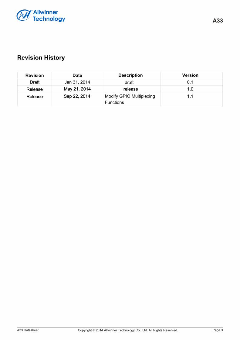
Revision History
Revision Date DescriptionDraft draft
Version0.1
Release May 21, 2014 release 1.0Release May 21, 2014 release 1.0Release Sep 22, 2014 1.1Release Sep 22, 2014 1.Modify GPIO Multiplexing
Functions

A33
A33 Datasheet Copyright © 2014 Allwinner Technology Co., Ltd. All Rights Reserved. Page 4
Table of Contents
CHAPTER 1 OVERVIEW ................ ...........................................................................................................................5
CHAPTER 2 FEATURES ............................... ............................................................................................................6
CHAPTER 3 BLOCK DIAGRAM .................. ........................................................................................................... 16
CHAPTER 4 PIN DESCRIPTION ................ ........................................................................................................... 17
4.1. PIN CHARACTERISTICS ........................ .......................................................................................................................17
4.2. GPIO MULTIPLEXING FUNCTIONS ......................... ......................................................................................................23
4.3. DETAILED PIN/SIGNAL DESCRIPTION ................... .......................................................................................................25
CHAPTER 5 ELECTRICAL CHARACTERISTICS ... ............................................................................................29
5.1. ABSOLUTE MAXIMUM RATINGS ............................................................................................ .....................................29
5.2. RECOMMENDED OPERATING CONDITIONS ...................................................................... .....................................29
5.3. DC ELECTRICAL CHARACTERISTICS .................................................................................................. .....................30
5.4. OSCILLATOR ELECTRICAL CHARACTERISTICS .....................................................................................................30
5.4.1. 24MHZ OSCILLATOR CHARACTERISTICS .......................................................................................................31
5.4.2. 32768HZ OSCILLATOR CHARACTERISTICS .....................................................................................................31
5.5. POWER UP/DOWN SEQUENCE ...................................................................................................................................32
CHAPTER 6 PIN ASSIGNMENT .............................................................................................................................33
6.1. PIN MAP .............................................................................................................................................................................33
6.2. PACKAGE DIMENSION ....................................................................................................................................................34

Device,USB Host,SD/MMC, I2S /PCM, SPI, thus significantly reducing system components required in design to
A33 Datasheet Copyright © 2014 Allwinner Technology Co., Ltd. All Rights Reserved. Page 5
Overview
1 OVERVIEW
The Allwinner A33 is a remarkably power-efficient quad-core tablet processor based on ARM CortexTM-A7 CPU along with Mali400MP2 GPU architecture. It is also highly competitive in terms of system cost thanks to its high system integration and is capable of delivering excellent user experience while maintaining ultra low power consumption.
Main features of A33 include:
● CPU architecture: A33 processor packs the most power efficient quad-core CortexTM-A7 CPU architecture deliver outstanding system performance and impressive battery life experience;
● Graphic: A33 adopts the extensively implemented and technically mature Mali400MP2 GPU to provide end users with superior experience in web browsing, video playback and games, etc.; OpenGL ES 2.0 and OpenVG 1.1 standards are supported;
● Video Engine: A33 supports high-definition 1080P video processing and various mainstream video standards such as H.264, VP8, MPEG 1/2/4, JPEG/MJPEG, etc.;
● Display: A33 supports CPU/RGB/LVDS LCD interface up to 1280x800 resolution. Four-lane MIPI DSI (Display Serial Interface) is integrated as well, supporting MIPI DSI V1.01 and MIPI D-PHY V1.00;
● Image: A33 supports a parallel CMOS sensor interface up to 5M resolution
Thanks to its advanced system design and outstanding software optimization, the A33 is capable of providing top-notch system performance with long-lasting battery life experience: in addition to its powerful yet energy-efficient CortexTM-A7 CPU architecture, advanced fabrication process, video acceleration hardware, DVFS technology support and high system integration, A33 also features a unique Talking Standby Mode where the processor can be inactive during voice calls to provide end users with ultra-long battery life experience. Additionally, Allwinner A33 features high system integration with a wide range of integrated I/Os like 4-lane MIPI DSI, LVDS, USB Dual Role
simplify product design and reduce total system costs.

A33 Datasheet Copyright © 2014 Allwinner Technology Co., Ltd. All Rights Reserved. Page 6
Features
2 FEATURES
2.1. CPU Architecture
The A33 platform is based on quad-core CortexTM-A7 CPU architecture.
● ARMv7 ISA standard instruction set plus Thumb-2 and Jazeller RCT ● NEON with SIMD and VFPv4 support ● Support hardware virtualization ● Support LPAE ● Support 4GB address space ● Support 256KB L1 cache and shared 512KB L2 cache ● Support DVFS with independent power domain
2.2. GPU ● Mali400MP2 GPU ● Support OpenGL ES 2.0 / OpenVG 1.1 standard

Support block size from 1 to 65535 bytes
Support Memory Dynamic Frequency Scale
Boot ROM
A33 Datasheet Copyright © 2014 Allwinner Technology Co., Ltd. All Rights Reserved. Page 7
Features
2.3. Memory Subsystem
This section consists of:
● ● SDRAM ● NAND Flash ● SD/MMC interface
Boot ROM ● Support system boot from Raw NAND, eMMC NAND, SPI NOR Flash, and SD/TF card ● Support system code download through USB DRD(Dual Role Device)
SDRAM ● Support 2GB address space ● Support 16-bit bus width ● Compatible with JEDEC standard DDR3 /DDR3L SDRAM
NAND Flash
● Comply to ONFI 2.3 and Toggle 1.0
● Support 64-bit ECC per 512 bytes or 1024 bytes
● Support 8-bit Raw NAND flash controller sharing pin with eMMC
● Support 2 CE and 2 RB signals
● Support SLC/MLC/TLC NAND and EF-NAND
SD/eMMC Interface
● Comply to eMMC standard specification V4.41, SD physical layer specification V2.0, SDIO card specification V2.0
● Support 4/8-bit bus width
● Support HS/DS bus mode
● Support 3 SD/eMMC controllers
● Support SDIO interrupt detection
●Support two ranks●Support 16 address signal lines and 3 bank signal lines●
● Support CRC generation and error detection●

A33 Datasheet Copyright © 2014 Allwinner Technology Co., Ltd. All Rights Reserved. Page 8
Features
2.4. System Peripheral
This section includes:
● Timer ● High Speed Timer ● RTC ● GIC ● DMA ● CCU ● PWM
Timer ● Support two timers: clock source can be switched over 24MHz and 32768Hz ● Support two 33-bit AVS counters ● Support one 64-bit system counter from 24MHz ● Support a watchdog to generate reset signal or interrupts
High Speed Timer ● Clock source is fixed to AHB, and the pre-scale ranges from 1 to 16 ● Support a 56-bit counter
RTC ● Support full clock features: second/minute/hour/day/month/year ● Support a 32768Hz clock fanout
GIC ● Support 16 SGIs, 16 PPIs and 128 SPIs ● Support ARM architecture security extensions ● Support ARM architecture virtualization extensions ● Support single processor and multiple processors environment
Support ECB,CBC,CTR,CTS modes for AES
Support clock gating control for individual components
Support data transfer types with memory-to-memory,memory-to-peripheral,peripheral-to-memory
Support Symmetrical Algorithm: AES,DES,3DES
SS
A33 Datasheet Copyright © 2014 Allwinner Technology Co., Ltd. All Rights Reserved. Page 9
Features
DMA ● 8-channel DMA ● Support data width of 8/16/32 bits ● Support linear and IO address modes
CCU ● 11 PLLs ● Support a 24MHz oscillator, a 32768Hz oscillator and an on-chip RC oscillator
PWM
● Support two PWM outputs
● Support cycle mode and pulse mode
● Support prescale from 1 to 16
●● Support Hash Algorithm:SHA-1, MD5 ● Support 160-bits hardware PRNG with 192-bits seed
Support ECB,CBC,CTR modes for DES/3DES●●● Support 128-bits, 192-bits and 256-bits key size for AES● 32-words RX FIFO and 32-words TX FIFO for high speed application● CPU mode and DMA mode operation
Security System2.5.
●
●● Clock generation,clock division,clock output

A33 Datasheet Copyright © 2014 Allwinner Technology Co., Ltd. All Rights Reserved. Page 10
Features
2.6. Display Subsystem
This section includes:
● Display engine ● Video output
Display Engine ● Four movable layers, each layer size up to 2048x2048 pixels ● Ultra-Scaling engine
–Support four-tap scale filter in both horizontal and vertical –Support input size up to 1920x1920 resolution and output size up to 1280x1280 resolution
● Support mult iple image input formats: mono 1/2/4/8bpp, palette 1/2/4/8bpp, 6/24/32bpp color,
YUV444/420/422/411
● Support alpha blending / color key / gamma
● Support output color correction: luminance / hue / saturation, etc
● Support Saturation Enhancement and Dynnmic Range Control
● Support realtime write back function
Video Output ● Support CPU / Sync RGB / LVDS LCD interface up to 1280x800 resolution ● Support 1/2/4-lane MIPI DSI interface up to 1280x800 resolution
–Support MIPI DSI V1.01 and MIPI D-PHY V1.00 –Support command mode and video mode (non-burst mode with sync pulses, non-burst mode with sync event and burst mode)
● Support RGB666 dither function

A33 Datasheet Copyright © 2014 Allwinner Technology Co., Ltd. All Rights Reserved. Page 11
Features
2.7. Video Engine
Video Decoding ● Support video playback up to 1920x1080@60fps ● Support multi-format video playback, including MPEG1/2, MPEG4 SP/ASP GMC, WMV9/VC1, H.263 including Sorenson Spark, H.264 BP/MP/HP, VP8, WMV9/VC-1, JPEG/MJPEG, etc
Video Encoding ● Support H.264 HP video encoding up to 1920x1080@60fps ● JPEG baseline: picture size up to 4080x4080 ● Support Alpha blending ● Support thumb generation ● Support 4x2 scaling ratio: from 1/16 to 64 arbitrary non-integer ratio

Video Input
A33 Datasheet Copyright © 2014 Allwinner Technology Co., Ltd. All Rights Reserved. Page 12
Features
2.8.
CSI ● Support parallel camera sensor ● Support 8-bit CCIR601/656 interface ● Support up to 5M pixel camera sensor ● Support dual outputs for display and encoding
2.9. Audio Subsystem
Audio Codec ● Support stereo audio DAC
–Up to 100dB SNR –8KHz ~ 192KHz DAC sample rate
● Support stereo audio ADC –Up to 92dB SNR –8KHz ~ 48KHz ADC sample rate
● Support four analog audio inputs –Two microphone differential inputs for main mic and headphone mic –One differential phone input for modem –One stereo line-in input for FM
● Support two analog audio outputs –One stereo or differential capless headphone output –One differential earpiece output
● Support Talking Standby Mode, where the application processor remains inactive during voice call application for power saving, support noise reduction
Support Dynamic Range Controller(DRC) adjusting the DAC playback output●Support Automatic Gain Control(AGC) adjusting the ADC recording output●Two PCM interface connected with BB and BT●

One 128x24-bits FIFO for data transmit,one 64x24-bits FIFO for data receive
Sample rate from 8KHz to 192KHz●
Support single key,normal key and continuous key
A33 Datasheet Copyright © 2014 Allwinner Technology Co., Ltd. All Rights Reserved. Page 13
Features
2.10 External Peripherals
This section includes:
● USB 2.0 DRD ● USB HOST ● LRADC ● Digital Audio Interface ● UART ● SPI ● Open-drain TWI ● RSBTM
USB 2.0 DRD ● Support High-Speed (HS, 480Mbps), Full-Speed (FS, 12Mbps), and Low-Speed (LS, 1.5Mbps) in Host mode ● Support High-Speed (HS, 480Mbps) and Full-Speed (FS, 12Mbps) in Device mode ● Support up to five configurable endpoints for bulk, isochronous, control and interrupt
USB Host ● EHCI/OHCI-compliant host ● USB2.0 PHY and HSIC
KEYADC ● 6-bit resolution
Digital Audio Interface ● Two I2S/PCM compliant digital audio interfaces for modem and bluetooth ● I2S or PCM configured by software ● Support 3 I2S Data formats:Standard I2S,Left Justified and Right Justified
● Support the embeded DMA
● Support High-Speed(HS,480Mbps),Full-Speed(FS,12Mbps), and Low-Speed(LS,1.5Mbps)Device● An internal DMA Controller for data transfer with memory
● Support hold key and continuous key●
●●
I2S supports 2 channels output and 2 channels inputPCM supports linear sample(8-bit or 16-bit), 8-bit u-law and A-law companded sample
● Support 16,20,24bits audio data resolutions●

Programmable output delay of CD signal
A33 Datasheet Copyright © 2014 Allwinner Technology Co., Ltd. All Rights Reserved. Page 14
Features
UART ● Support six UART controllers ● FIFO size up to 64 bytes ● Support speed up to 3MHz
SPI
● Two SPI controllers
● Full-duplex synchronous serial interface
TWI
● Up to four TWI(Two Wire Interface) controllers
● Support one dedicated TWI controller for CSI
● Support speed up to 400Kbps
RSBTM (Reduced Serial Bus)
● Support transfer speed up to 20MHz
Master/Slave configurable●Polarity and phase of the Chip Select and SPI Clock are configurable●
● Compliant with industry-standard 16550 UARTs● Support Infrared Data Association(IrDA)1.0 SIR
● Two 64-bytes FIFO for SPI-TX and SPI-RX operation● DMA-based or interrupt-based operation
● Master/Slave configurable● Allows 10-bits addressing transactions
● Support Push-Pull bus● Support Host mode● Support multiple devices●
Parity check for address and data transmission●
A33 Datasheet Copyright © 2014 Allwinner Technology Co., Ltd. All Rights Reserved. Page 15
Features
2.11. Power Management ● Support DVFS for CPU frequency and voltage adjustment ● Support super standby mode for energy efficiency ● Support talking standby mode for energy efficiency during voice call application
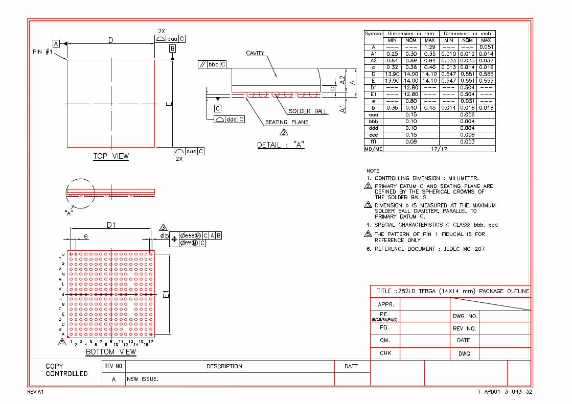
2.12. Package ● TFBGA 282 balls,0.8mm ball pitch, 14 x 14 x 1.4-mm

A33 Datasheet Copyright © 2014 Allwinner Technology Co., Ltd. All Rights Reserved. Page 16
Block Diagram
3 BLOCK DIAGRAM
A33 Block Diagram

A33 Datasheet Copyright © 2014 Allwinner Technology Co., Ltd. All Rights Reserved. Page 17
Pin Description
4 PIN DESCRIPTION
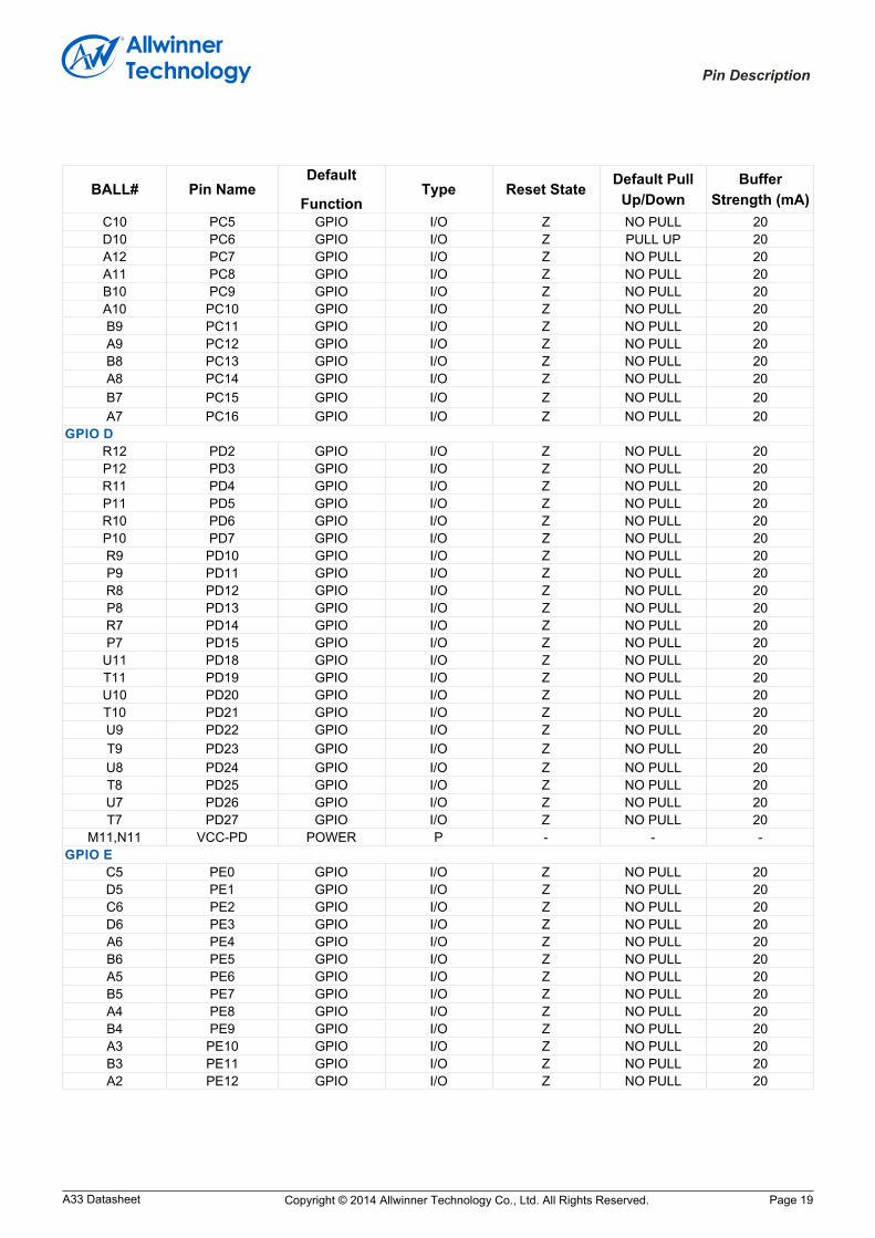
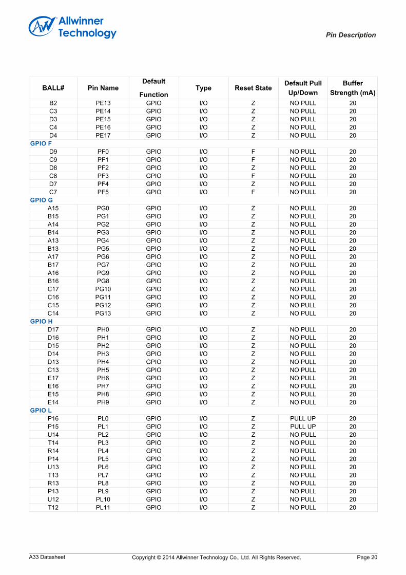
4.1. PIN CHARACTERISTICSFollowing table describes the A33 pin characteristics from seven aspects: BALL#, Pin Name, Default Function1, Type2, Reset State3, Default Pull Up/Down4, and Buffer Strength5.
BALL# Pin NameDefault
FunctionType Reset State Default Pull
Up/DownBuffer
Strength (mA)SDRAM
M1 DQ0 DRAM I/O Z - -M2 DQ1 DRAM I/O Z - -L1 DQ2 DRAM I/O Z - -L2 DQ3 DRAM I/O Z - -J1 DQ4 DRAM I/O Z - -J2 DQ5 DRAM I/O Z - -H1 DQ6 DRAM I/O Z - -H2 DQ7 DRAM I/O Z - -U3 DQ8 DRAM I/O Z - -U1 DQ9 DRAM I/O Z - -U2 DQ10 DRAM I/O Z - -T2 DQ11 DRAM I/O Z - -R2 DQ12 DRAM I/O Z - -P1 DQ13 DRAM I/O Z - -P2 DQ14 DRAM I/O Z - -N1 DQ15 DRAM I/O Z - -M4 DVREF DRAM P - - -R1 DQS1 DRAM I/O Z - -T1 DQS1B DRAM I/O Z - -T3 DQM1 DRAM O Z - -K2 DQS0 DRAM I/O Z - -K1 DQS0B DRAM I/O Z - -N2 DQM0 DRAM O Z - -
Note:
1 Default function defines the default function of each pin, especially for pins with multiplexing functions;2 There are five pin types here: O for output, I for input, I/O for input/output, A for analog,OD for Open-Drain, P for power and G for ground;3 Reset state defines the state of the terminal at reset: Z for high-impedance,F for Multiplexing Function Pin;4 Default Pull up/down defines the presence of an internal pull up or pull down resistor. Unless otherwise speci-fied, the pin is default to be floating, and can be configured as pull up or pull down;5 Buffer strength defines the driver strength of the associated output buffer. It is tested in the condition that VCC= 3.0V, strength=MAX;

A33 Datasheet Copyright © 2014 Allwinner Technology Co., Ltd. All Rights Reserved. Page 18
Pin Description
BALL# Pin NameDefault
FunctionType Reset State Default Pull
Up/DownBuffer
Strength (mA)G2 DCKB DRAM O Z - -G1 DCK DRAM O Z - -J4 DCKE DRAM O Z - -N7 DCKE1 DRAM O Z - -E4 DA0 DRAM O Z - -D1 DA1 DRAM O Z - -F2 DA2 DRAM O Z - -H3 DA3 DRAM O Z - -D2 DA4 DRAM O Z - -F1 DA5 DRAM O Z - -A1 DA6 DRAM O Z - -G4 DA7 DRAM O Z - -B1 DA8 DRAM O Z - -F4 DA9 DRAM O Z - -E2 DA10 DRAM O Z - -C2 DA11 DRAM O Z - -E1 DA12 DRAM O Z - -F3 DA13 DRAM O Z - -C1 DA14 DRAM O Z - -E3 DA15 DRAM O Z - -J3 DBA0 DRAM O Z - -K4 DBA1 DRAM O Z - -H4 DBA2 DRAM O Z - -K3 DWE DRAM O Z - -M3 DCAS DRAM O Z - -L4 DRAS DRAM O Z - -N3 DCS DRAM O Z - -N5 DCS1 DRAM O Z - -L3 DODT DRAM O Z - -L7 DODT1 DRAM O Z - -R3 DZQ DRAM A Z - -G3 DRST DRAM O Z - -P3 VDD-DLL POWER P - - -
H5,J5,K5,L5,
H6,J6VCC-DRAM POWER P - - -
GPIO BG17 PB0 GPIO I/O Z NO PULL 20G16 PB1 GPIO I/O Z NO PULL 20F17 PB2 GPIO I/O Z NO PULL 20F16 PB3 GPIO I/O Z NO PULL 20G14 PB4 GPIO I/O Z NO PULL 20G15 PB5 GPIO I/O Z NO PULL 20F14 PB6 GPIO I/O Z NO PULL 20F15 PB7 GPIO I/O Z NO PULL 20
GPIO CD12 PC0 GPIO I/O Z NO PULL 20C12 PC1 GPIO I/O Z NO PULL 20C11 PC2 GPIO I/O Z NO PULL 20D11 PC3 GPIO I/O Z PULL UP 20B11 PC4 GPIO I/O Z PULL UP 20
A33 Datasheet Copyright © 2014 Allwinner Technology Co., Ltd. All Rights Reserved. Page 19
Pin Description
BALL# Pin NameDefault
FunctionType Reset State Default Pull
Up/DownBuffer
Strength (mA)C10 PC5 GPIO I/O Z NO PULL 20D10 PC6 GPIO I/O Z PULL UP 20A12 PC7 GPIO I/O Z NO PULL 20A11 PC8 GPIO I/O Z NO PULL 20B10 PC9 GPIO I/O Z NO PULL 20A10 PC10 GPIO I/O Z NO PULL 20B9 PC11 GPIO I/O Z NO PULL 20A9 PC12 GPIO I/O Z NO PULL 20B8 PC13 GPIO I/O Z NO PULL 20A8 PC14 GPIO I/O Z NO PULL 20B7 PC15 GPIO I/O Z NO PULL 20A7 PC16 GPIO I/O Z NO PULL 20
GPIO DR12 PD2 GPIO I/O Z NO PULL 20P12 PD3 GPIO I/O Z NO PULL 20R11 PD4 GPIO I/O Z NO PULL 20P11 PD5 GPIO I/O Z NO PULL 20R10 PD6 GPIO I/O Z NO PULL 20P10 PD7 GPIO I/O Z NO PULL 20R9 PD10 GPIO I/O Z NO PULL 20P9 PD11 GPIO I/O Z NO PULL 20R8 PD12 GPIO I/O Z NO PULL 20P8 PD13 GPIO I/O Z NO PULL 20R7 PD14 GPIO I/O Z NO PULL 20P7 PD15 GPIO I/O Z NO PULL 20
U11 PD18 GPIO I/O Z NO PULL 20T11 PD19 GPIO I/O Z NO PULL 20U10 PD20 GPIO I/O Z NO PULL 20T10 PD21 GPIO I/O Z NO PULL 20U9 PD22 GPIO I/O Z NO PULL 20T9 PD23 GPIO I/O Z NO PULL 20U8 PD24 GPIO I/O Z NO PULL 20T8 PD25 GPIO I/O Z NO PULL 20U7 PD26 GPIO I/O Z NO PULL 20T7 PD27 GPIO I/O Z NO PULL 20
M11,N11 VCC-PD POWER P - - -GPIO E
C5 PE0 GPIO I/O Z NO PULL 20D5 PE1 GPIO I/O Z NO PULL 20C6 PE2 GPIO I/O Z NO PULL 20D6 PE3 GPIO I/O Z NO PULL 20A6 PE4 GPIO I/O Z NO PULL 20B6 PE5 GPIO I/O Z NO PULL 20A5 PE6 GPIO I/O Z NO PULL 20B5 PE7 GPIO I/O Z NO PULL 20A4 PE8 GPIO I/O Z NO PULL 20B4 PE9 GPIO I/O Z NO PULL 20A3 PE10 GPIO I/O Z NO PULL 20B3 PE11 GPIO I/O Z NO PULL 20A2 PE12 GPIO I/O Z NO PULL 20
A33 Datasheet Copyright © 2014 Allwinner Technology Co., Ltd. All Rights Reserved. Page 20
Pin Description
BALL# Pin NameDefault
FunctionType Reset State Default Pull
Up/DownBuffer
Strength (mA)B2 PE13 GPIO I/O Z NO PULL 20C3 PE14 GPIO I/O Z NO PULL 20D3 PE15 GPIO I/O Z NO PULL 20C4 PE16 GPIO I/O Z NO PULL 20D4 PE17 GPIO I/O Z NO PULL 20
GPIO FD9 PF0 GPIO I/O F NO PULL 20C9 PF1 GPIO I/O F NO PULL 20D8 PF2 GPIO I/O Z NO PULL 20C8 PF3 GPIO I/O F NO PULL 20D7 PF4 GPIO I/O Z NO PULL 20C7 PF5 GPIO I/O F NO PULL 20
GPIO GA15 PG0 GPIO I/O Z NO PULL 20B15 PG1 GPIO I/O Z NO PULL 20A14 PG2 GPIO I/O Z NO PULL 20B14 PG3 GPIO I/O Z NO PULL 20A13 PG4 GPIO I/O Z NO PULL 20B13 PG5 GPIO I/O Z NO PULL 20A17 PG6 GPIO I/O Z NO PULL 20B17 PG7 GPIO I/O Z NO PULL 20A16 PG9 GPIO I/O Z NO PULL 20B16 PG8 GPIO I/O Z NO PULL 20C17 PG10 GPIO I/O Z NO PULL 20C16 PG11 GPIO I/O Z NO PULL 20C15 PG12 GPIO I/O Z NO PULL 20C14 PG13 GPIO I/O Z NO PULL 20
GPIO HD17 PH0 GPIO I/O Z NO PULL 20D16 PH1 GPIO I/O Z NO PULL 20D15 PH2 GPIO I/O Z NO PULL 20D14 PH3 GPIO I/O Z NO PULL 20D13 PH4 GPIO I/O Z NO PULL 20C13 PH5 GPIO I/O Z NO PULL 20E17 PH6 GPIO I/O Z NO PULL 20E16 PH7 GPIO I/O Z NO PULL 20E15 PH8 GPIO I/O Z NO PULL 20E14 PH9 GPIO I/O Z NO PULL 20
GPIO LP16 PL0 GPIO I/O Z PULL UP 20P15 PL1 GPIO I/O Z PULL UP 20U14 PL2 GPIO I/O Z NO PULL 20T14 PL3 GPIO I/O Z NO PULL 20R14 PL4 GPIO I/O Z NO PULL 20P14 PL5 GPIO I/O Z NO PULL 20U13 PL6 GPIO I/O Z NO PULL 20T13 PL7 GPIO I/O Z NO PULL 20R13 PL8 GPIO I/O Z NO PULL 20P13 PL9 GPIO I/O Z NO PULL 20U12 PL10 GPIO I/O Z NO PULL 20T12 PL11 GPIO I/O Z NO PULL 20

A33 Datasheet Copyright © 2014 Allwinner Technology Co., Ltd. All Rights Reserved. Page 21
Pin Description
BALL# Pin NameDefault
FunctionType Reset State Default Pull
Up/DownBuffer
Strength (mA)SYSTEM CONTROL
N14 NMI - I Z NO PULL -P17 RESET - I Z NO PULL -
USBT16 USB-DM0 - A - - -T17 USB-DP0 - A - - -U16 USB-DM1 - A - - -U17 USB-DP1 - A - - -L12 VCC-USB - P - - -
HSICN12 VCC-HSIC - P - - -T15 HSIC-STR - A - - -U15 HSIC-DAT - A - - -
AUDIO CODECM16 MIC1N - A - - -M17 MIC1P - A - - -N16 MIC2N - A - - -N17 MIC2P - A - - -J15 LINEINR - A - - -H15 LINEINL - A - - -K16 VRA1 - A - - -K17 VRA2 - A - - -L16 AVCC - P - - -L17 VRP - A - - -N15 PHONEOUTN - A - - -M15 PHONEOUTP - A - - -K15 PHONEINN - A - - -L15 PHONEINP - A - - -J14 HBIAS - A - - -K14 MBIAS - A - - -H13 AGND - G - - -J16 HPOUTR - A - - -J17 HPOUTL - A - - -H14 HPCOM - A - - -H16 HPCOMFB - A - - -H17 HPVCCBP - P - - -K13 HPVCCIN - P - - -
LRADCL14 LRADC0 - A - - -
DSIR4 DSI-D0N - A - - -P4 DSI-D0P - A - - -R5 DSI-D1N - A - - -P5 DSI-D1P - A - - -U6 DSI-D2N - A - - -T6 DSI-D2P - A - - -R6 DSI-D3N - A - - -P6 DSI-D3P - A - - -U5 DSI-CKN - A - - -T5 DSI-CKP - A - - -N6 VCC-DSI - P - - -

A33 Datasheet Copyright © 2014 Allwinner Technology Co., Ltd. All Rights Reserved. Page 22
Pin Description
BALL# Pin NameDefault
FunctionType Reset State Default Pull
Up/DownBuffer
Strength (mA)CLOCK
R17 X32KIN - A - - -R16 X32KOUT - A - - -R15 X32KFOUT - A - - -M13 RTCVIO - P - - -M12 VCC-RTC - P - - -U4 X24MIN - A - - -T4 X24MOUT - A - - -M5 VCC-PLL - P - - -
POWERM8 VCC-EFUSE - P - - -
M14 VDD-CPUS - P - - -E5,E6,E7,F5,F6,
F7,G5,G6VDD-CPU - P - - -
E8,E9,E10,K6,L6,M6,M7,N8
N9,N10VDD-SYS - P - - -
E11,E12,F11F12,G12
VCC-IO - P - - -
N4,F8,F9,F10,G7,G8,G9,G10,
G11,H7,H8,H9,H10,H11,H12,J7,J8,J9,J10,J11,J12
K7,K8,K9,K10,K11,K12,
L8,L9,L10,L11,M9,M10
GND - G - - -

A33 Datasheet Copyright © 2014 Allwinner Technology Co., Ltd. All Rights Reserved. Page 23
Pin Description
4.2. GPIO MULTIPLEXING FUNCTIONSFollowing table provides a description of the GPIO multiplexing functions of A33.
PortDefault
FunctionIO Type Default
IO StateDefault Pull Up/Down
Multiplexed Function 2
Multiplexed Function 3
Multiplexed Function 4
PB0 GPIO I/O DIS Z UART2-TX UART0-TX PB-EINT0PB1 GPIO I/O DIS Z UART2-RX UART0-RX PB-EINT1PB2 GPIO I/O DIS Z UART2-RTS - PB-EINT2PB3 GPIO I/O DIS Z UART2-CTS - PB-EINT3PB4 GPIO I/O DIS Z PCM0-SYNC AIF2-SYNC PB-EINT4PB5 GPIO I/O DIS Z PCM0-BCLK AIF2-BCLK PB-EINT5PB6 GPIO I/O DIS Z PCM0-DOUT AIF2-DOUT PB-EINT6PB7 GPIO I/O DIS Z PCM0-DIN AIF2-DIN PB-EINT7PC0 GPIO I/O DIS Z NAND-WE SPI0-MOSI -PC1 GPIO I/O DIS Z NAND-ALE SPI0-MISO -PC2 GPIO I/O DIS Z NAND-CLE SPI0-CLK -PC3 GPIO I/O DIS Pull-up NAND-CE1 SPI0-CS -PC4 GPIO I/O DIS Pull-up NAND-CE0 - -PC5 GPIO I/O DIS Z NAND-RE SDC2-CLK -PC6 GPIO I/O DIS Pull-up NAND-RB0 SDC2-CMD -PC7 GPIO I/O DIS Pull-up NAND-RB1 - -PC8 GPIO I/O DIS Z NAND-DQ0 SDC2-D0 -PC9 GPIO I/O DIS Z NAND-DQ1 SDC2-D1 -PC10 GPIO I/O DIS Z NAND-DQ2 SDC2-D2 -PC11 GPIO I/O DIS Z NAND-DQ3 SDC2-D3 -PC12 GPIO I/O DIS Z NAND-DQ4 SDC2-D4 -PC13 GPIO I/O DIS Z NAND-DQ5 SDC2-D5 -PC14 GPIO I/O DIS Z NAND-DQ6 SDC2-D6 -PC15 GPIO I/O DIS Z NAND-DQ7 SDC2-D7 -PC16 GPIO I/O DIS Z NAND-DQS SDC2-RST -PD2 GPIO I/O DIS Z LCD-D2 SDC1-CLK -PD3 GPIO I/O DIS Z LCD-D3 SDC1-CMD -PD4 GPIO I/O DIS Z LCD-D4 SDC1-D0 -PD5 GPIO I/O DIS Z LCD-D5 SDC1-D1 -PD6 GPIO I/O DIS Z LCD-D6 SDC1-D2 -PD7 GPIO I/O DIS Z LCD-D7 SDC1-D3 -PD10 GPIO I/O DIS Z LCD-D10 UART1-TX -PD11 GPIO I/O DIS Z LCD-D11 UART1-RX -PD12 GPIO I/O DIS Z LCD-D12 UART1-RTS -PD13 GPIO I/O DIS Z LCD-D13 UART1-CTS -PD14 GPIO I/O DIS Z LCD-D14 -PD15 GPIO I/O DIS Z LCD-D15 -PD18 GPIO I/O DIS Z LCD-D18 LVDS-VP0 -PD19 GPIO I/O DIS Z LCD-D19 LVDS-VN0 -PD20 GPIO I/O DIS Z LCD-D20 LVDS-VP1 -PD21 GPIO I/O DIS Z LCD-D21 LVDS-VN1 -PD22 GPIO I/O DIS Z LCD-D22 LVDS-VP2 -PD23 GPIO I/O DIS Z LCD-D23 LVDS-VN2 -PD24 GPIO I/O DIS Z LCD-CLK LVDS-VPC -PD25 GPIO I/O DIS Z LCD-DE LVDS-VNC -

A33 Datasheet Copyright © 2014 Allwinner Technology Co., Ltd. All Rights Reserved. Page 24
Pin Description
PD26 GPIO I/O DIS Z LCD-HSYNC LVDS-VP3 -PD27 GPIO I/O DIS Z LCD-VSYNC LVDS-VN3 -PE0 GPIO I/O DIS Z CSI-PCLK - -PE1 GPIO I/O DIS Z CSI-MCLK - -PE2 GPIO I/O DIS Z CSI-HSYNC - -PE3 GPIO I/O DIS Z CSI-VSYNC - -PE4 GPIO I/O DIS Z CSI-D0 - -PE5 GPIO I/O DIS Z CSI-D1 - -PE6 GPIO I/O DIS Z CSI-D2 - -PE7 GPIO I/O DIS Z CSI-D3 - -PE8 GPIO I/O DIS Z CSI-D4 - -PE9 GPIO I/O DIS Z CSI-D5 - -PE10 GPIO I/O DIS Z CSI-D6 - -PE11 GPIO I/O DIS Z CSI-D7 - -PE12 GPIO I/O DIS Z CSI-SCK TWI2-SCK -PE13 GPIO I/O DIS Z CSI-SDA TWI2-SDA -PE14 GPIO I/O DIS Z - - -PE15 GPIO I/O DIS Z - - -PE16 GPIO I/O DIS Z - - -PE17 GPIO I/O DIS Z - - -PF0 GPIO I/O JTAG F SDC0-D1 JTAG-MS1 -PF1 GPIO I/O JTAG F SDC0-D0 JTAG-DI1 -PF2 GPIO I/O DIS Z SDC0-CLK UART0-TX -PF3 GPIO I/O JTAG F SDC0-CMD JTAG-DO1 -PF4 GPIO I/O DIS Z SDC0-D3 UART0-RX -PF5 GPIO I/O JTAG F SDC0-D2 JTAG-CK1 -PG0 GPIO I/O DIS Z SDC1-CLK - PG-EINT0PG1 GPIO I/O DIS Z SDC1-CMD - PG-EINT1PG2 GPIO I/O DIS Z SDC1-D0 - PG-EINT2PG3 GPIO I/O DIS Z SDC1-D1 - PG-EINT3PG4 GPIO I/O DIS Z SDC1-D2 - PG-EINT4PG5 GPIO I/O DIS Z SDC1-D3 - PG-EINT5PG6 GPIO I/O DIS Z UART1-TX - PG-EINT6PG7 GPIO I/O DIS Z UART1-RX - PG-EINT7PG8 GPIO I/O DIS Z URAT1-RTS - PG-EINT8PG9 GPIO I/O DIS Z UART1-CTS - PG-EINT9PG10 GPIO I/O DIS Z PCM1-SYNC AIF3-SYNC PG-EINT10PG11 GPIO I/O DIS Z PCM1-BCLK AIF3-BCLK PG-EINT11PG12 GPIO I/O DIS Z PCM1-DOUT AIF3-DOUT PG-EINT12PG13 GPIO I/O DIS Z PCM1-DIN AIF3-DIN PG-EINT13PH0 GPIO I/O DIS Z PWM0 - -PH1 GPIO I/O DIS Z PWM1 - -PH2 GPIO I/O DIS Z TWI0-SCK - -PH3 GPIO I/O DIS Z TWI0-SDA - -PH4 GPIO I/O DIS Z TWI1-SCK - -PH5 GPIO I/O DIS Z TWI1-SDA - -PH6 GPIO I/O DIS Z SPI0-CS UART3-TX -PH7 GPIO I/O DIS Z SPI0-CLK UART3-RX -PH8 GPIO I/O DIS Z SPI0-MOSI UART3-RTS -PH9 GPIO I/O DIS Z SPI0-MISO UART3-CTS -PL0 GPIO I/O DIS Pull-up S-RSB-SCK S-TWI-SCK S-PL-EINT0PL1 GPIO I/O DIS Pull-up S-RSB-SDA S-TWI-SDA S-PL-EINT1PL2 GPIO I/O DIS Z S-UART-TX - S-PL-EINT2PL3 GPIO I/O DIS Z S-UART-RX - S-PL-EINT3PL4 GPIO I/O DIS Z - S-PL-EINT4S-JTAG-MS

A33 Datasheet Copyright © 2014 Allwinner Technology Co., Ltd. All Rights Reserved. Page 25
Pin Description
PL5 GPIO I/O DIS Z - S-PL-EINT5PL6 GPIO I/O DIS Z - S-PL-EINT6PL7 GPIO I/O DIS Z - S-PL-EINT7PL8 GPIO I/O DIS Z S-TWI-SCK - S-PL-EINT8PL9 GPIO I/O DIS Z S-TWI-SDA - S-PL-EINT9PL10 GPIO I/O DIS Z S-PWM - S-PL-EINT10PL11 GPIO I/O DIS Z - - S-PL-EINT11
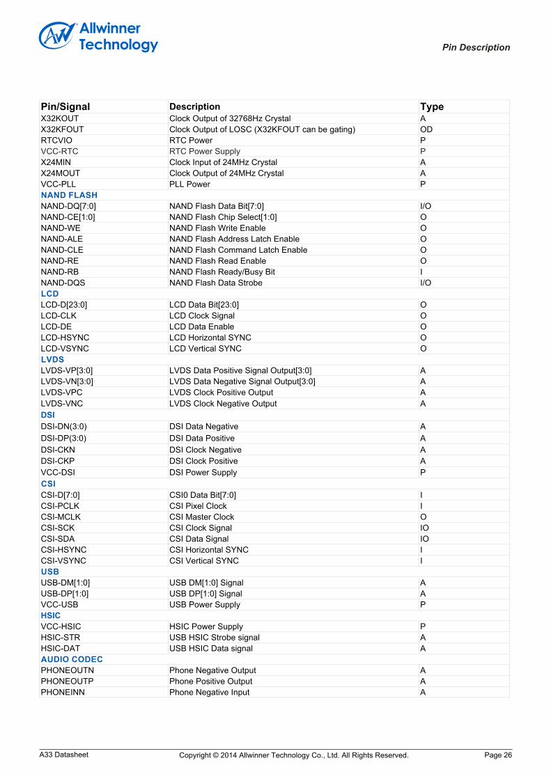
4.3. DETAILED PIN/SIGNAL DESCRIPTION
Pin/Signal Description TypeDRAMDQ[15:0] DRAM DQ[15:0] I/ODVREF DRAM Reference Input PDQS[1:0] DRAM Data Strobe DQS[1:0] I/ODQSB[1:0] DRAM Data Strobe DQSB[1:0] I/ODCK DRAM Clock ODCKB DRAM CKB ODCKE[1:0] DRAM Clock Enable [1:0] ODA[15:0] DRAM Data Address[15:0] ODBA[2:0] DRAM Bank Address[2:0] ODWE DRAM Write Enable ODCAS DRAM Column Address Strobe ODRAS DRAM Row Address Strobe ODCS[1:0] DRAM Chip Select[1:0] ODODT[1:0] DRAM ODT Control [1:0] ODZQ DRAM ZQ Calibration ADRST DRAM Reset OVDD-DLL DLL Power Supply PVCC-DRAM DRAM Power Supply PGPIOPB[7:0] Port B Bit[7:0] I/OPC[18:0] Port C Bit[18:0] I/OPD[27:0] Port D Bit[27:0] I/OVCC-PD Port D Power Supply PPE[17:0] Port E Bit[17:0] I/OPF[5:0] Port F Bit[5:0] I/OPG[13:0] Port G Bit[13:0] I/OPH[9:0] Port H Bit[9:0] I/OPL[11:0] Port L Bit[11:0] I/OSYSTEM CONTROLNMI Non-Maskable Interrupt IRESET Reset Signal IINTERRUPTEINT External Interrupt IPWMPWM[1:0] PWM OCLOCKX32KIN Clock Input of 32768Hz Crystal A
S-JTAG-CKS-JTAG-DOS-JTAG-DI
A33 Datasheet Copyright © 2014 Allwinner Technology Co., Ltd. All Rights Reserved. Page 26
Pin Description
Pin/Signal Description TypeX32KOUT Clock Output of 32768Hz Crystal AX32KFOUT Clock Output of LOSC (X32KFOUT can be gating) ODRTCVIO RTC Power PVCC-RTC RTC Power Supply PX24MIN Clock Input of 24MHz Crystal AX24MOUT Clock Output of 24MHz Crystal AVCC-PLL PLL Power PNAND FLASHNAND-DQ[7:0] NAND Flash Data Bit[7:0] I/ONAND-CE[1:0] NAND Flash Chip Select[1:0] ONAND-WE NAND Flash Write Enable ONAND-ALE NAND Flash Address Latch Enable ONAND-CLE NAND Flash Command Latch Enable ONAND-RE NAND Flash Read Enable ONAND-RB NAND Flash Ready/Busy Bit INAND-DQS NAND Flash Data Strobe I/OLCDLCD-D[23:0] LCD Data Bit[23:0] OLCD-CLK LCD Clock Signal OLCD-DE LCD Data Enable OLCD-HSYNC LCD Horizontal SYNC OLCD-VSYNC LCD Vertical SYNC OLVDS LVDS-VP[3:0] LVDS Data Positive Signal Output[3:0] ALVDS-VN[3:0] LVDS Data Negative Signal Output[3:0] ALVDS-VPC LVDS Clock Positive Output ALVDS-VNC LVDS Clock Negative Output ADSIDSI-DN(3:0) DSI Data Negative ADSI-DP(3:0) DSI Data Positive ADSI-CKN DSI Clock Negative ADSI-CKP DSI Clock Positive AVCC-DSI DSI Power Supply PCSICSI-D[7:0] CSI0 Data Bit[7:0] ICSI-PCLK CSI Pixel Clock ICSI-MCLK CSI Master Clock OCSI-SCK CSI Clock Signal IOCSI-SDA CSI Data Signal IOCSI-HSYNC CSI Horizontal SYNC ICSI-VSYNC CSI Vertical SYNC IUSBUSB-DM[1:0] USB DM[1:0] Signal AUSB-DP[1:0] USB DP[1:0] Signal AVCC-USB USB Power Supply PHSICVCC-HSIC HSIC Power Supply PHSIC-STR USB HSIC Strobe signal AHSIC-DAT USB HSIC Data signal AAUDIO CODECPHONEOUTN Phone Negative Output APHONEOUTP Phone Positive Output APHONEINN Phone Negative Input A

A33 Datasheet Copyright © 2014 Allwinner Technology Co., Ltd. All Rights Reserved. Page 27
Pin Description
Pin/Signal Description TypePHONEINP Phone Positive Input AMICINN[2:1] MIC Negative Input AMICINP[2:1] MIC Positive Input ALINEINR Line-in Right Input ALINEINL Line-in Left Input AHBIAS HBIAS AMBIAS MBIAS AVRA1 Reference Voltage AVRA2 Reference Voltage AAVCC Analog Power Supply PVRP Reference Voltage AAGND Analog Ground GHPOUTR Headphone Right Channel Output AHPOUTL Headphone Left Channel Output AHPVCCIN Headphone VCC Input AHPVCCBP Headphone VCC Bypass AHPCOM Headphone Common Reference AHPCOMFB Headphone Common Reference Feedback AHPBP Headphone Bypass Output AAIF-SYNC Audio Codec SYNC Signal AAIF-BCLK Audio Codec Clock Signal AAIF-DOUT Audio Codec Data Output AAIF-DIN Audio Codec Data Input ALRADCLRADC0 LRADC Input ASPISPI0-CS SPI Chip Select Signal I/OSPI0-CLK SPI Clock Signal I/OSPI0-MOSI SPI Master Data Out, Slave Data In I/OSPI0-MISO SPI Master Data In, Slave Data Out I/OUART
(x=[3:0])UARTx-TX UART Data Transmit OUARTx-RX UART Data Receive IUARTx-RTS UART Data Request to Send OUARTx-CTS UART Data Clear to Send ITWI
(x=[2:0])(Open-Drain)TWIx-SCK TWI Clock Signal I/OTWIx-SDA TWI Data Signal I/OSD/MMC
(x=[2:0])SDCx-D SD/MMC/SDIO Data Bit I/OSDCx-CLK SD/MMC/SDIO Clock OSDCx-CMD SD/MMC/SDIO Command Signal I/OSDC-RST SD/MMC/SDIO Reset Signal OPCM(x=[1:0])PCMx-SYNC PCM SYNC I/OPCMx-CLK PCM Clock I/OPCMx-DOUT PCM Data Output OPCMx-DIN PCM Data Input IRSBS-RSB-SCK RSB Clock OS-RSB-SDA RSB Data I/O

A33 Datasheet Copyright © 2014 Allwinner Technology Co., Ltd. All Rights Reserved. Page 28
Pin Description
Pin/Signal Description TypePOWERVDD-CPU CPU Power Supply PVDD-CPUS CPUS Power Supply PVDD-SYS System Power Supply PVCC-EFUSE EFUSE Power Supply pGND Ground GVCC-IO IO Power Supply P

T
A33 Datasheet Copyright © 2014 Allwinner Technology Co., Ltd. All Rights Reserved. Page 29
Electrical Characteristics
5 ELECTRICAL CHARACTERISTICS
5.1. ABSOLUTE MAXIMUM RATINGSFunctional operation of the device at these or any other conditions beyond those indicated under Recommended Operating Conditions is not implied. Exposure to absolute maximum rated conditions for extended periods may af-fect device reliability.
SYMBOL PARAMETER MIN MAX UNITSTG Storage Temperature -40 125 °C
II/O In/Out current for input and output -40 40 mAVESD ESD stress voltage -4000 +4000 VESD
VCC-IO DC Supply Voltage for I/O -0.3 3.6 VVDD-DLL Power Supply for DLL -0.3 2.75 V
VCC-DRAM Power Supply for DRAM -0.3 1.65 V
VCC-PLL Power Supply for PLL -0.3 3.6 V
VCC-RTC Power Supply for RTC -0.3 3.6 VAVCC DC Supply Voltage for Analog Part -0.3 3.6 VVCC-USB Power Supply for USB PHY -0.3 3.6 VVCC-DSI Power Supply for DSI -0.3 3.6 VVDD-CPU Power Supply for CPU -0.3 1.5 VVDD-SYS Power Supply for System -0.3 1.5 V
5.2. RECOMMENDED OPERATING CONDITIONS
SYMBOL PARAMETER MIN TYP MAX UNIT
Ta
Ambient Operating Temperature[Commercial] -20 - 75 °COperating Temperature[Extended] - - - °C
VCC-IO DC Supply Voltage for I/O 1.7 1.8~3.3 3.6 V

3.3
1.575
2.35
A33 Datasheet Copyright © 2014 Allwinner Technology Co., Ltd. All Rights Reserved. Page 30
Electrical Characteristics
SYMBOL PARAMETER MIN TYP MAX UNITVDD-DLL Power Supply for DLL 2.5 2.65 V
VCC-DRAMPower Supply for DRAM (DDR3L) 1.283 1.35 1.575 VPower Supply for DRAM (DDR3) 1.425 1.5 V
VCC-PLL Power Supply for PLL 2.7 3.0 3.3 VVCC-USB Power Supply for USB PHY 3.0 3.3 3.45 VVCC-RTC Power Supply for RTC 2.7 3.0 3.3 VAVCC DC Supply Voltage for Analog Part 2.7 3.0 3.3 VVCC-DSI Power Supply for MIPI DSI 2.7 3.6 VVDD-CPU Power Supply for CPU 0.9 1.1 1.4 VVDD-SYS Power Supply for System 0.9 1.1 1.4 V
5.3. DC ELECTRICAL CHARACTERISTICS
SYMBOL PARAMETER TEST CONDITIONS MIN TYP MAX UNITVIH High-Level Input Voltage VCC-IO=3.0V 0.7 x VCC-IO - VCC-IO + 0.3 VVIL Low-Level Input Voltage VCC-IO=3.0V -0.3 - 0.3 x VCC-IO V
VHYS Hysteresis Voltage - 0.1 x VCC-IO - - VIIH High-Level Input Current VCC-IO=3.0V, VI=3.0V -10 - 10 uAIIL Low-Level Input Current VCC-IO=3.0V, VI=0V -10 - 10 uAVOH High-Level Output Voltage VCC-IO=3.0V VCC-IO - 0.2 - - VVOL Low-Level Output Voltage VCC-IO=3.0V - - 0.2 VIOZ Tri-State Output Leakage Current VCC-IO=3.0V -10 - 10 uACIN Input Capacitance - - - 5 pFCOUT Output Capacitance - - - 5 pF
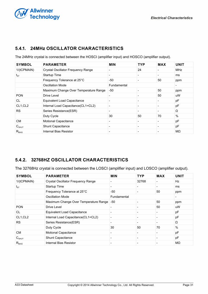
5.4.
OSCILLATOR ELECTRICAL CHARACTERISTICSThe A33 contains two oscillators: a 24MHz oscillator and a 32768Hz oscillator. Each oscillator requires a specific crystal.
The A33 device operation requires following two input clocks:
● The 32768Hz frequency is used for low frequency operation.
● The 24MHz frequency is used to generate the main source clock of the A33 device.
RPU Input pull-up resistance VCC-IO=3.0V 50 100 150 KRPD Input pull-down resistance VCC-IO=3.0V 50 100 150 K
A33 Datasheet Copyright © 2014 Allwinner Technology Co., Ltd. All Rights Reserved. Page 31
Electrical Characteristics
5.4.1. 24MHz OSCILLATOR CHARACTERISTICSThe 24MHz crystal is connected between the HOSCI (amplifier input) and HOSCO (amplifier output).
SYMBOL PARAMETER MIN TYP MAX UNIT1/(tCPMAIN) Crystal Oscillator Frequency Range - 24 - MHztST Startup Time - - - ms
Frequency Tolerance at 25°C -50 - 50 ppmOscillation Mode Fundamental -Maximum Change Over Temperature Range -50 - 50 ppm
PON Drive Level - - 50 uWCL Equivalent Load Capacitance - - - pFCL1,CL2 Internal Load Capacitance(CL1=CL2) - - - pFRS Series Resistance(ESR) - - - Ω
Duty Cycle 30 50 70 %CM Motional Capacitance - - - pFCSHUT Shunt Capacitance - - - pFRBIAS Internal Bias Resistor - - - MΩ
5.4.2. 32768HZ OSCILLATOR CHARACTERISTICS
The 32768Hz crystal is connected between the LOSCI (amplifier input) and LOSCO (amplifier output).
SYMBOL PARAMETER MIN TYP MAX UNIT1/(tCPMAIN) Crystal Oscillator Frequency Range - 32768 - HztST Startup Time - - - ms
Frequency Tolerance at 25°C -50 - 50 ppmOscillation Mode Fundamental -Maximum Change Over Temperature Range -50 - 50 ppm
PON Drive Level - - 50 uWCL Equivalent Load Capacitance - - - pFCL1,CL2 Internal Load Capacitance(CL1=CL2) - - - pFRS Series Resistance(ESR) - - - Ω
Duty Cycle 30 50 70 %CM Motional Capacitance - - - pFCSHUT Shunt Capacitance - - - pFRBIAS Internal Bias Resistor - - - MΩ

A33 Datasheet Copyright © 2014 Allwinner Technology Co., Ltd. All Rights Reserved. Page 32
Electrical Characteristics
5.5. POWER UP/DOWN SEQUENCEThe external voltage regulator and other power-on devices must provide the processor with a specific sequence of power and resets to ensure proper operations.
A33 Datasheet Copyright ©2014 Allwinner Technology Co., Ltd. All Rights Reserved.
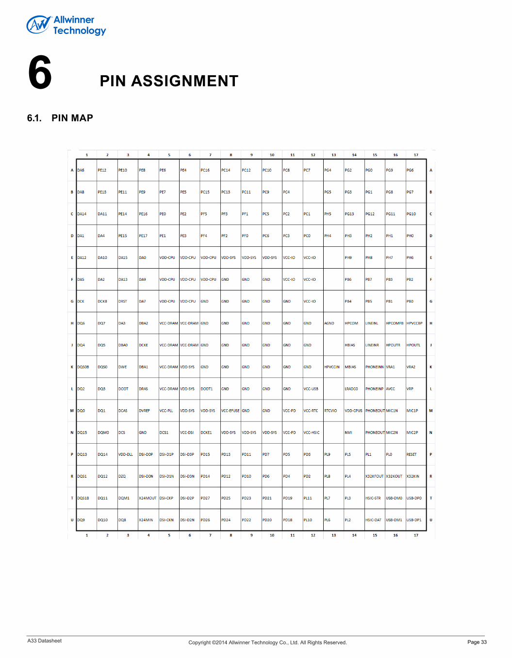
6 PIN ASSIGNMENT
6.1. PIN MAP
Page 33
A33
A33 Datasheet Copyright © 2014 Allwinner Technology Co., Ltd. All Rights Reserved. Page 35
Copyright © 2014 Allwinner Technology Co., Ltd. All Rights Reserved.
Allwinner Technology Co., Ltd.
No.9 Technology Road 2,High-Tech Zone
Zhuhai, Guangdong Province, China
Contact Us: [email protected]
www.allwinnertech.com