allen and holberg - cmos analog circuit design
DESCRIPTION
cmos analog circuit designhas a detaled description of the analog circuit designTRANSCRIPT
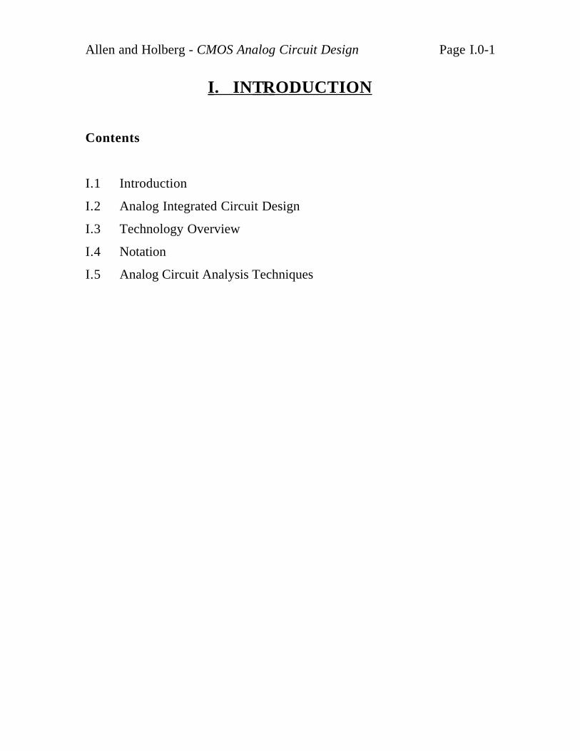
Allen and Holberg - CMOS Analog Circuit Design Page I.0-1
I. INT RODUCTION
Contents
I.1 Introduction
I.2 Analog Integrated Circuit Design
I.3 Technology Overview
I.4 Notation
I.5 Analog Circuit Analysis Techniques
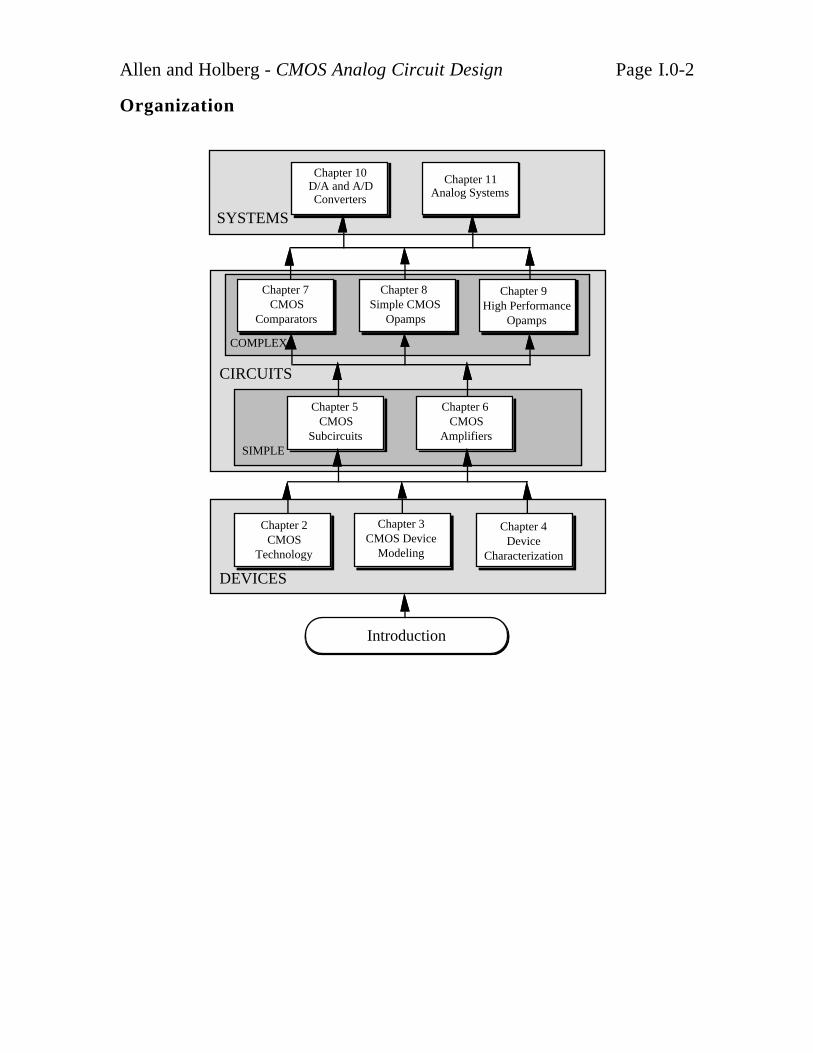
Allen and Holberg - CMOS Analog Circuit Design Page I.0-2
Organization
DEVICES
SYSTEMS
CIRCUITS
Chapter 2CMOS
Technology
Chapter 3CMOS Device
Modeling
Chapter 4Device
Characterization
Chapter 7 CMOS
Comparators
Chapter 8 Simple CMOS
Opamps
Chapter 9 High Performance
Opamps
Chapter 5 CMOS
Subcircuits
Chapter 6 CMOS
Amplifiers
Chapter 10D/A and A/D Converters
Chapter 11Analog Systems
SIMPLE
COMPLEX
Introduction

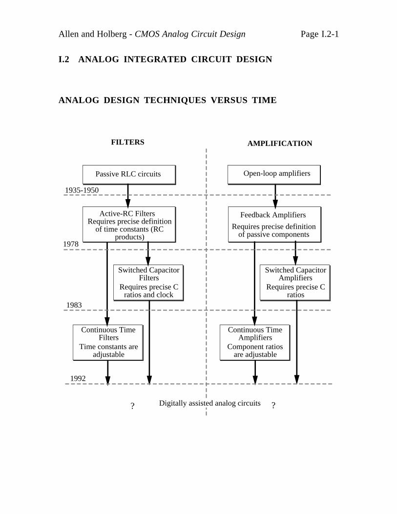
Allen and Holberg - CMOS Analog Circuit Design Page I.2-1
I.1 - INTRODUCTION
GLOBAL OBJECTIVES
• Teach the analysis, modeling, simulation, and design of analog circuits
implemented in CMOS technology.
• Emphasis will be on the design methodology and a hierarchical
approach to the subject.
SPECIFIC OBJECTIVES
1. Present an overall, uniform viewpoint of CMOS analog circuit design.
2. Achieve an understanding of analog circuit design.
• Hand calculations using simple models
• Emphasis on insight
• Simulation to provide second-order design resolution
3. Present a hierarchical approach.
• Sub-blocks → Blocks → Circuits → Systems
4. Examples to illustrate the concepts.
Allen and Holberg - CMOS Analog Circuit Design Page I.2-1
I.2 ANALOG INTEGRATED CIRCUIT DESIGN
ANALOG DESIGN TECHNIQUES VERSUS TIME
Requires precise definitionof time constants (RC
products)
FILTERS AMPLIFICATION
Passive RLC circuits Open-loop amplifiers
Active-RC Filters Feedback Amplifiers
Requires precise definitionof passive components
Switched Capacitor Filters
Requires precise Cratios and clock
Switched Capacitor Amplifiers
Requires precise Cratios
Continuous Time Filters
Time constants are adjustable
Continuous Time Amplifiers
Component ratios are adjustable
1978
1983
1935-1950
1992
? ?Digitally assisted analog circuits

Allen and Holberg - CMOS Analog Circuit Design Page I.2-2
DISCRETE VS. INTEGRATED ANALOG CIRCUIT DESIGN
Activity/Item Discrete Integrated
Component Accuracy Well known Poor absolute accuracies
Breadboarding? Yes No (kit parts)
Fabrication Independent Very Dependent
Physical
Implementation
PC layout Layout, verification, and
extraction
Parasitics Not Important Must be included in the
design
Simulation Model parameters well
known
Model parameters vary
widely
Testing Generally complete
testing is possible
Must be considered
before the design
CAD Schematic capture,
simulation, PC board
layout
Schematic capture,
simulation, extraction,
LVS, layout and routing
Components All possible Active devices,
capacitors, and resistors
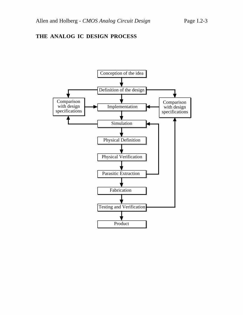
Allen and Holberg - CMOS Analog Circuit Design Page I.2-3
THE ANALOG IC DESIGN PROCESS
Conception of the idea
Definition of the design
Implementation
Simulation
Physical Verification
Parasitic Extraction
Fabrication
Testing and Verification
Product
Comparisonwith design
specifications
Comparisonwith design
specifications
Physical Definition
Allen and Holberg - CMOS Analog Circuit Design Page I.2-4
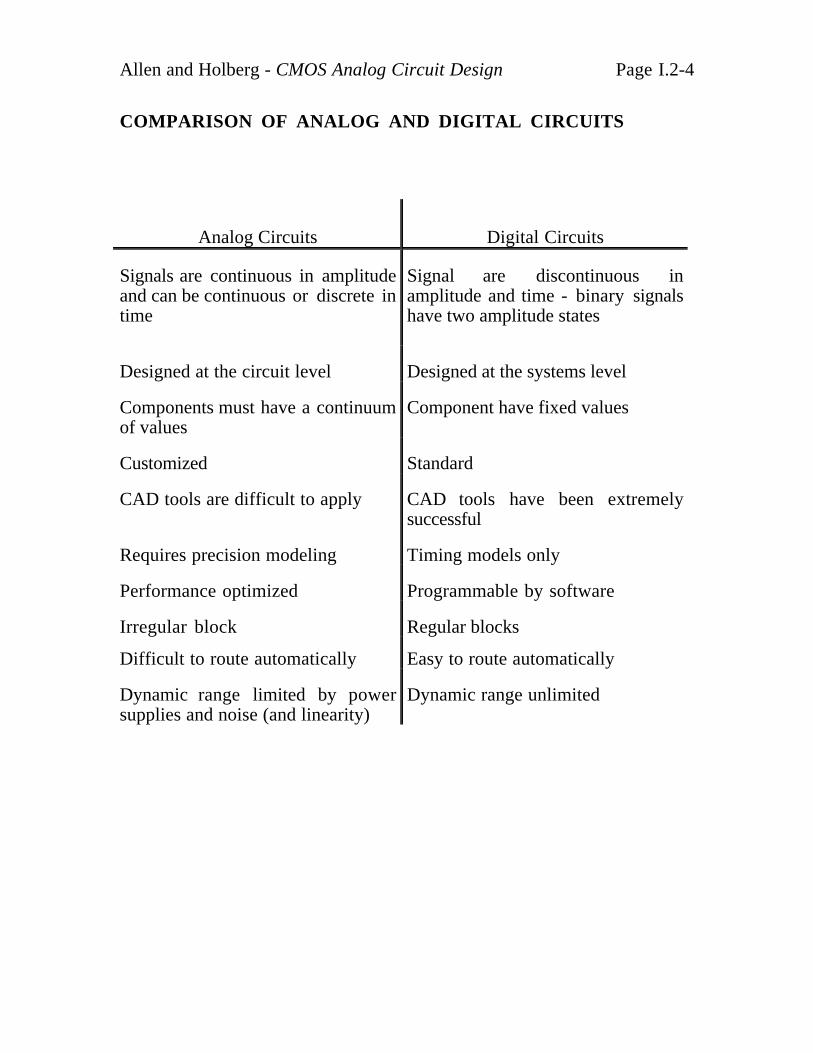
COMPARISON OF ANALOG AND DIGITAL CIRCUITS
Analog Circuits Digital Circuits
Signals are continuous in amplitudeand can be continuous or discrete intime
Signal are discontinuous inamplitude and time - binary signalshave two amplitude states
Designed at the circuit level Designed at the systems level
Components must have a continuumof values
Component have fixed values
Customized Standard
CAD tools are difficult to apply CAD tools have been extremelysuccessful
Requires precision modeling Timing models only
Performance optimized Programmable by software
Irregular block Regular blocks
Difficult to route automatically Easy to route automatically
Dynamic range limited by powersupplies and noise (and linearity)
Dynamic range unlimited
Allen and Holberg - CMOS Analog Circuit Design Page I.3-1
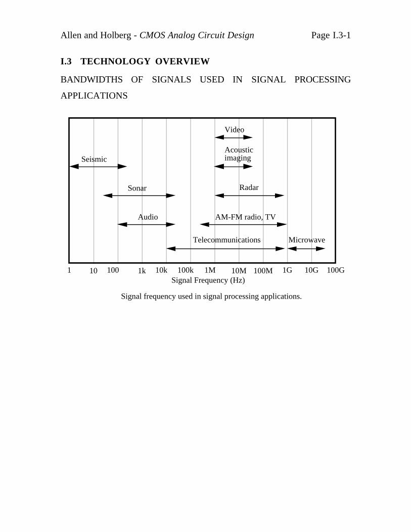
I.3 TECHNOLOGY OVERVIEW
BANDWIDTHS OF SIGNALS USED IN SIGNAL PROCESSING
APPLICATIONS
101 100 1k 10k 100k 1M 10M 100M 1G 10G 100G
Seismic
Sonar
Audio
Video
Acousticimaging
Radar
AM-FM radio, TV
Telecommunications Microwave
Signal Frequency (Hz)
Signal frequency used in signal processing applications.
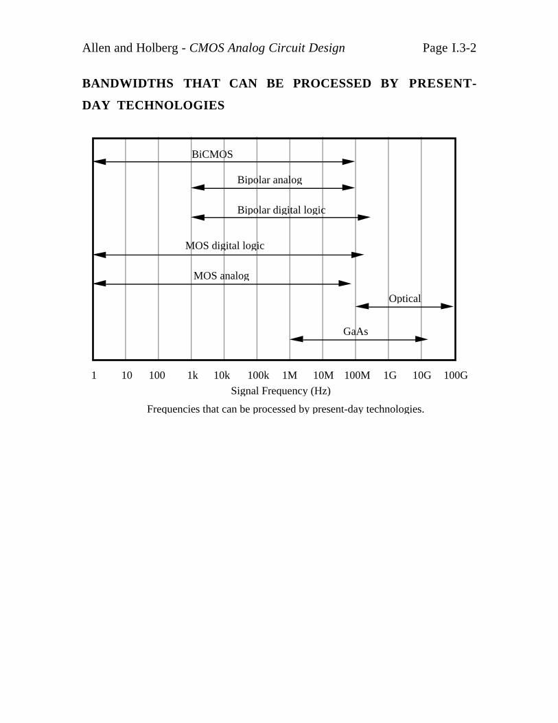
Allen and Holberg - CMOS Analog Circuit Design Page I.3-2
BANDWIDTHS THAT CAN BE PROCESSED BY PRESENT-
DAY TECHNOLOGIES
Frequencies that can be processed by present-day technologies.
101 100 1k 10k 100k 1M 10M 100M 1G 10G 100G
Signal Frequency (Hz)
GaAs
Optical
MOS digital logic
Bipolar digital logic
Bipolar analog
MOS analog
BiCMOS
Allen and Holberg - CMOS Analog Circuit Design Page I.3-3
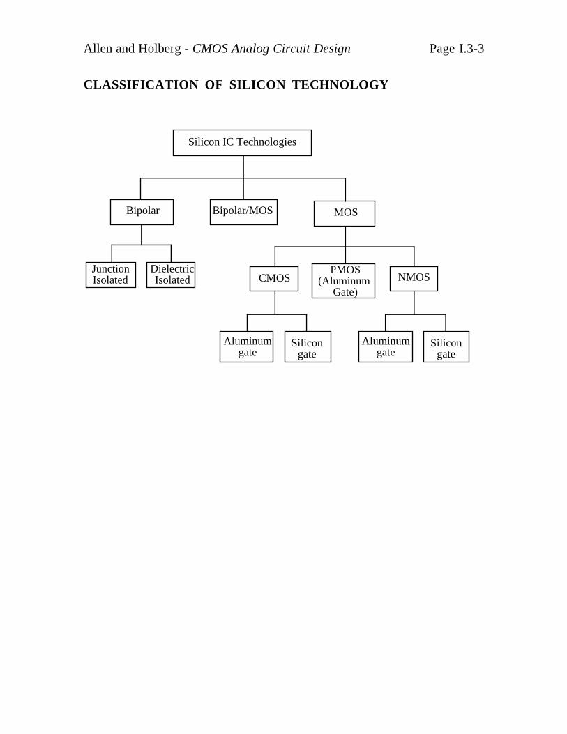
CLASSIFICATION OF SILICON TECHNOLOGY
Silicon IC Technologies
Bipolar Bipolar/MOS MOS
JunctionIsolated
Dielectric Isolated CMOS
PMOS(Aluminum
Gate)NMOS
Aluminum gate
Silicon gate
Aluminum gate
Silicon gate

Allen and Holberg - CMOS Analog Circuit Design Page I.3-4
BIPOLAR VS. MOS TRANSISTORS
CATEGORY BIPOLAR CMOS
Turn-on Voltage 0.5-0.6 V 0.8-1 V
Saturation Voltage 0.2-0.3 V 0.2-0.8 V
gm at 100µA 4 mS 0.4 mS (W=10L)
Analog SwitchImplementation
Offsets, asymmetric Good
Power Dissipation Moderate to high Low but can be large
Speed Faster Fast
Compatible Capacitors Voltage dependent Good
AC PerformanceDependence
DC variables only DC variables andgeometry
Number of Terminals 3 4
Noise (1/f) Good Poor
Noise Thermal OK OK
Offset Voltage < 1 mV 5-10 mV
Allen and Holberg - CMOS Analog Circuit Design Page I.3-5
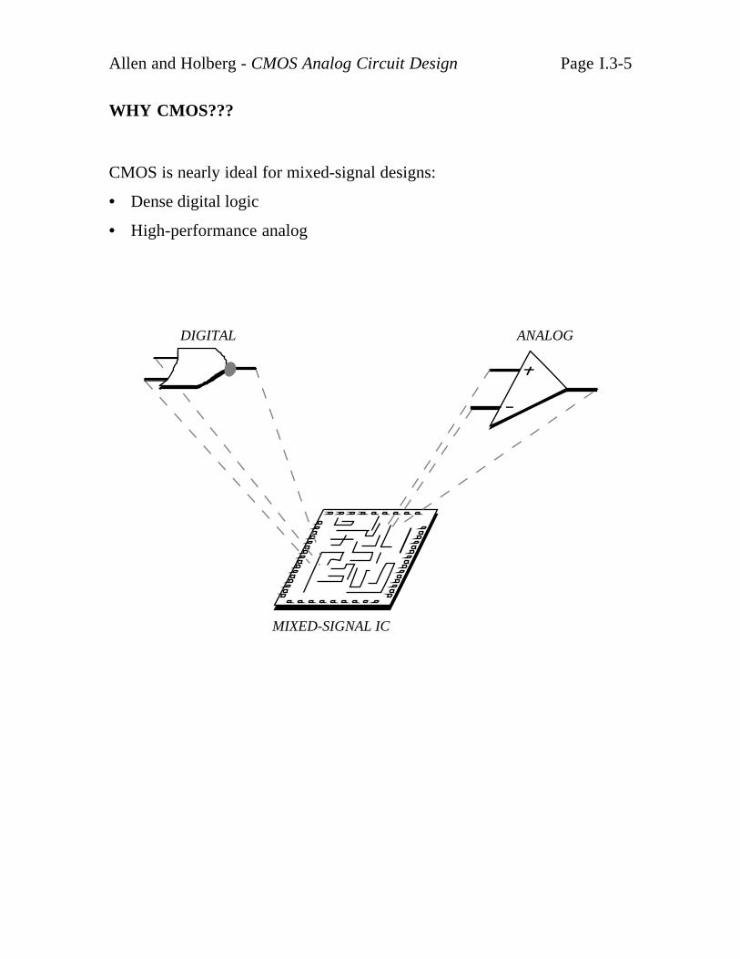
WHY CMOS???
CMOS is nearly ideal for mixed-signal designs:
• Dense digital logic
• High-performance analog
DIGITAL ANALOG
MIXED-SIGNAL IC
Allen and Holberg - CMOS Analog Circuit Design Page I.4-1
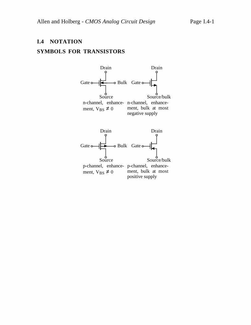
I.4 NOTATION
SYMBOLS FOR TRANSISTORS
Drain
Gate
Source/bulk
Drain
Gate
Source
Bulk
n-channel, enhance-ment, VBS ≠ 0
n-channel, enhance-ment, bulk at mostnegative supply
Drain
Gate
Source/bulk
Drain
Gate
Source
Bulk
p-channel, enhance-ment, VBS ≠ 0
p-channel, enhance-ment, bulk at mostpositive supply
Allen and Holberg - CMOS Analog Circuit Design Page I.4-2
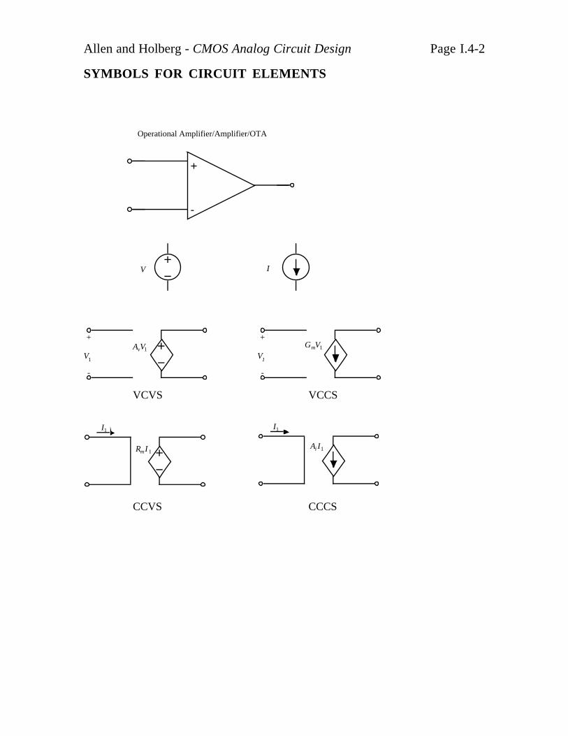
SYMBOLS FOR CIRCUIT ELEMENTS
+
-
A V+
-
G V
R I
I
A I
+
-
m 1
1
V1
v 1
I1
V1
m 1
i 1
V I
Operational Amplifier/Amplifier/OTA
VCVS VCCS
CCVS CCCS
Allen and Holberg - CMOS Analog Circuit Design Page I.4-3
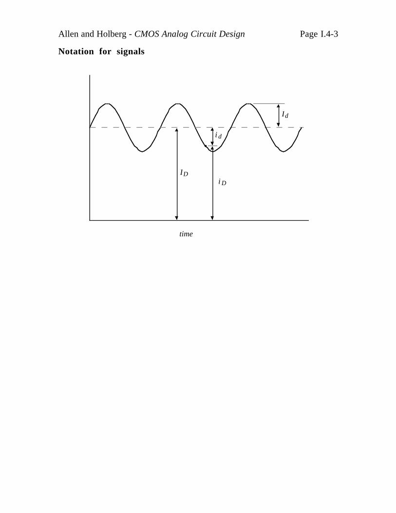
Notation for signals
ID
Id
i d
i D
time
Allen and Holberg - CMOS Analog Circuit Design Page II.0-1
II. CMOS TECHNOLOGY
Contents
II.1 Basic Fabrication Processes
II.2 CMOS Technology
II.3 PN Junction
II.4 MOS Transistor
II.5 Passive Components
II.6 Latchup Protection
II.7 ESD Protection
II.8 Geometrical Considerations
Allen and Holberg - CMOS Analog Circuit Design Page II.0-2
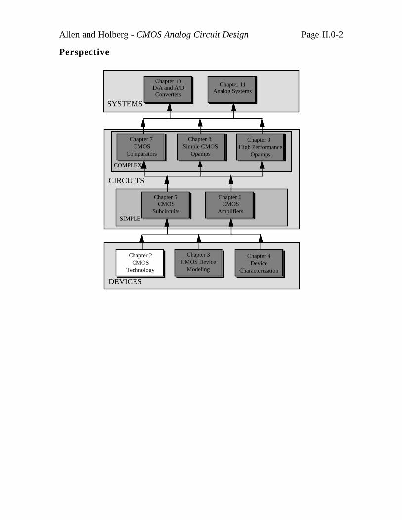
Perspective
DEVICES
SYSTEMS
CIRCUITS
Chapter 2CMOS
Technology
Chapter 3CMOS Device
Modeling
Chapter 4Device
Characterization
Chapter 7 CMOS
Comparators
Chapter 8 Simple CMOS
Opamps
Chapter 9 High Performance
Opamps
Chapter 5 CMOS
Subcircuits
Chapter 6 CMOS
Amplifiers
Chapter 10D/A and A/D Converters
Chapter 11Analog Systems
SIMPLE
COMPLEX

Allen and Holberg - CMOS Analog Circuit Design Page II.0-3
OBJECTIVE
• Provide an understanding of CMOS technology sufficient to enhance
circuit design.
• Characterize passive components compatible with basic technologies.
• Provide a background for modeling at the circuit level.
• Understand the limits and constraints introduced by technology.

Allen and Holberg - CMOS Analog Circuit Design Page II.1-1
II.1 - BASIC FABRICATION PROCESSES
BASIC FABRTICATION PROCESSES
Basic Steps
• Oxide growth
• Thermal diffusion
• Ion implantation
• Deposition
• Etching
Photolithography
Means by which the above steps are applied to selected areas of the silicon
wafer.
Silicon wafer0.5-0.8 mm
125-200 mm
n-type: 3-5 Ω -cm
p-type: 14-16 Ω -cm
Allen and Holberg - CMOS Analog Circuit Design Page II.1-2
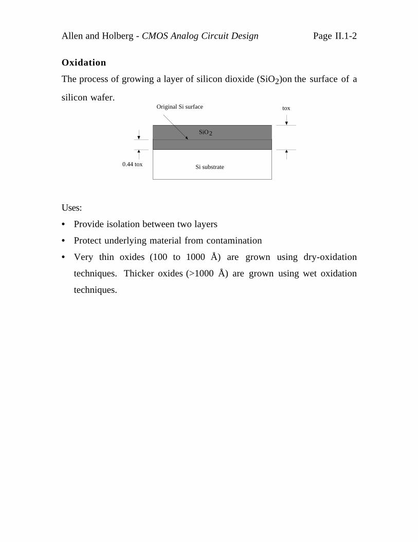
Oxidation
The process of growing a layer of silicon dioxide (SiO2)on the surface of a
silicon wafer.Original Si surface
0.44 tox
tox
Si substrate
SiO2
Uses:
• Provide isolation between two layers
• Protect underlying material from contamination
• Very thin oxides (100 to 1000 Å) are grown using dry-oxidation
techniques. Thicker oxides (>1000 Å) are grown using wet oxidation
techniques.
Allen and Holberg - CMOS Analog Circuit Design Page II.1-3
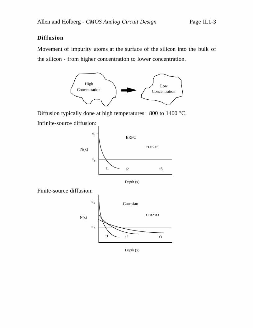
Diffusion
Movement of impurity atoms at the surface of the silicon into the bulk of
the silicon - from higher concentration to lower concentration.
LowConcentration
High
Concentration
Diffusion typically done at high temperatures: 800 to 1400 °C.
Infinite-source diffusion:
N(x)
Depth (x)
ERFC
t1<t2<t3
t1 t2 t3
NB
N0
Finite-source diffusion:
Depth (x)
t1<t2<t3
t1 t2 t3
Gaussian
N(x)
NB
N0
Allen and Holberg - CMOS Analog Circuit Design Page II.1-4
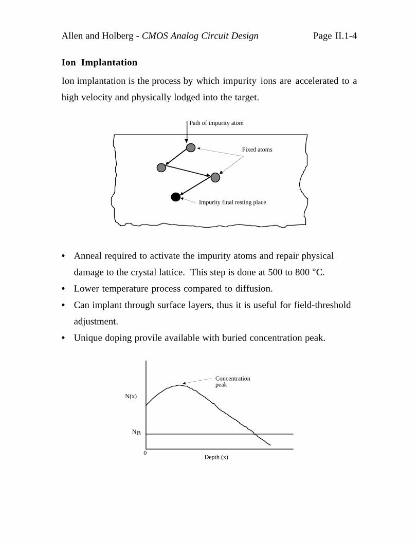
Ion Implantation
Ion implantation is the process by which impurity ions are accelerated to a
high velocity and physically lodged into the target.
Fixed atoms
Path of impurity atom
Impurity final resting place
• Anneal required to activate the impurity atoms and repair physical
damage to the crystal lattice. This step is done at 500 to 800 °C.
• Lower temperature process compared to diffusion.
• Can implant through surface layers, thus it is useful for field-threshold
adjustment.
• Unique doping provile available with buried concentration peak.
N(x)
N
Depth (x)0
Concentrationpeak
B
Allen and Holberg - CMOS Analog Circuit Design Page II.1-5
Deposition
Deposition is the means by which various materials are deposited on the
silicon wafer.
Examples:
• Silicon nitride (Si3N4)
• Silicon dioxide (SiO2)
• Aluminum
• Polysilicon
There are various ways to deposit a meterial on a substrate:
• Chemical-vapor deposition (CVD)
• Low-pressure chemical-vapor deposition (LPCVD)
• Plasma-assisted chemical-vapor deposition (PECVD)
• Sputter deposition
Materials deposited using these techniques cover the entire wafer.
Allen and Holberg - CMOS Analog Circuit Design Page II.1-6
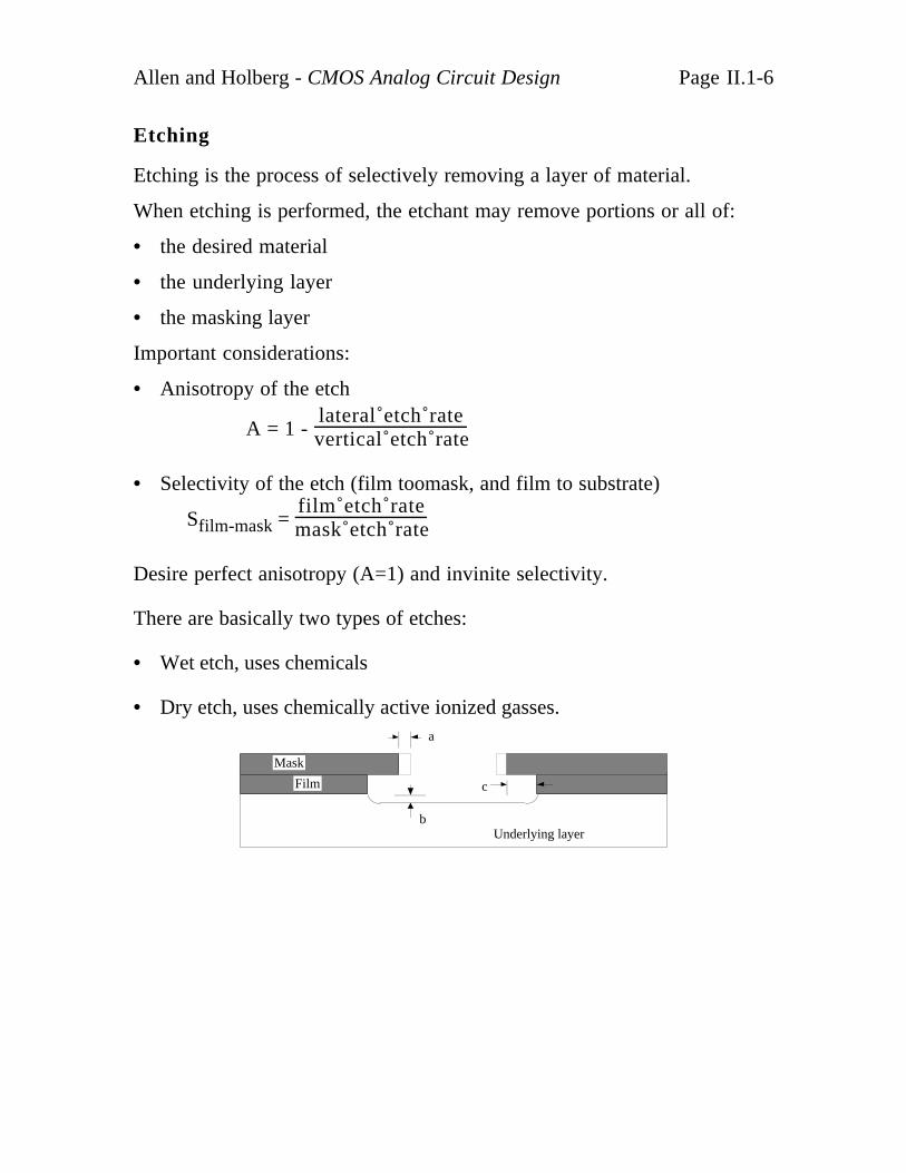
Etching
Etching is the process of selectively removing a layer of material.
When etching is performed, the etchant may remove portions or all of:
• the desired material
• the underlying layer
• the masking layer
Important considerations:
• Anisotropy of the etch
A = 1 - lateral etch ratevertical etch rate
• Selectivity of the etch (film toomask, and film to substrate)
Sfilm-mask = film etch ratemask etch rate
Desire perfect anisotropy (A=1) and invinite selectivity.
There are basically two types of etches:
• Wet etch, uses chemicals
• Dry etch, uses chemically active ionized gasses.
Mask
Film
bUnderlying layer
a
c

Allen and Holberg - CMOS Analog Circuit Design Page II.1-7
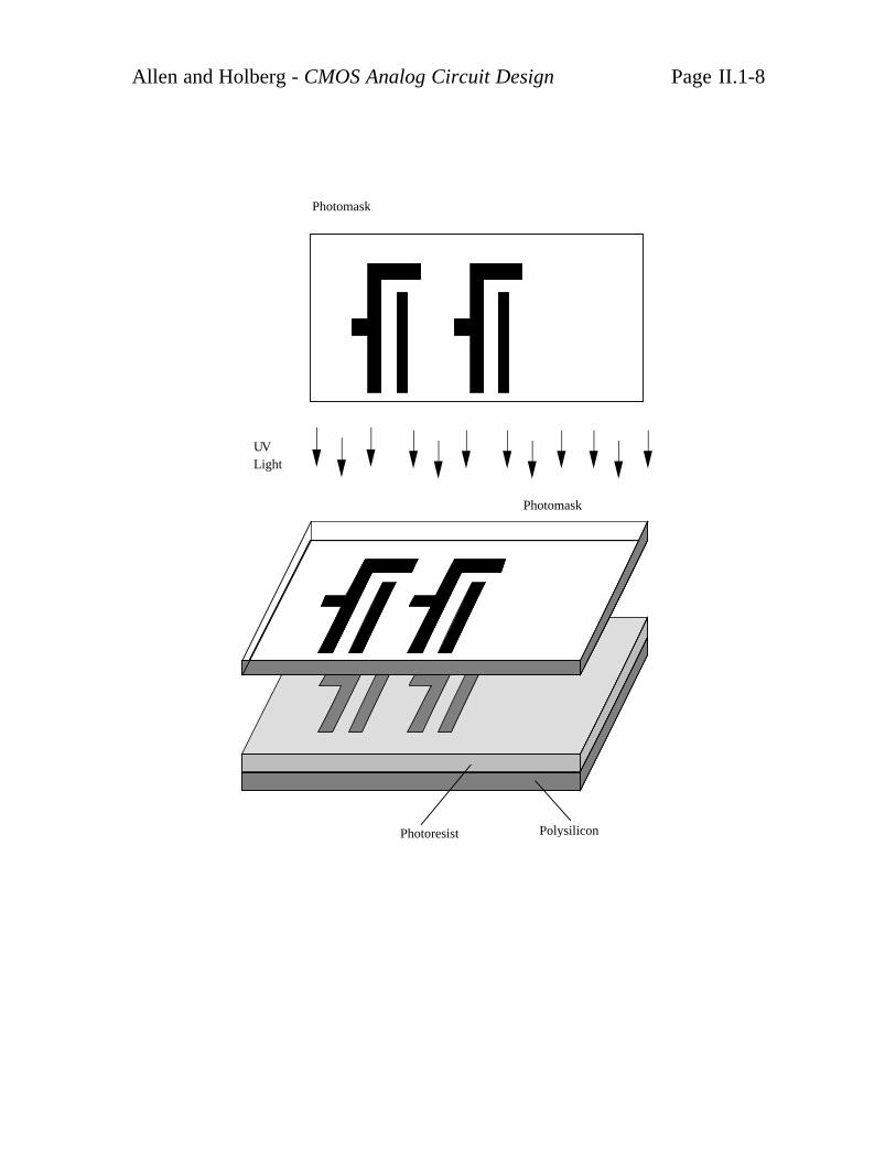
Photolithography
Components
• Photoresist material
• Photomask
• Material to be patterned (e.g., SiO2)
Positive photoresist-
Areas exposed to UV light are soluble in the developer
Negative photoresist-
Areas not exposed to UV light are soluble in the developer
Steps:
1. Apply photoresist
2. Soft bake
3. Expose the photoresist to UV light through photomask
4. Develop (remove unwanted photoresist)
5. Hard bake
6. Etch the exposed layer
7. Remove photoresist
Allen and Holberg - CMOS Analog Circuit Design Page II.1-8
Photoresist
Photomask
UVLight
Photomask
Polysilicon
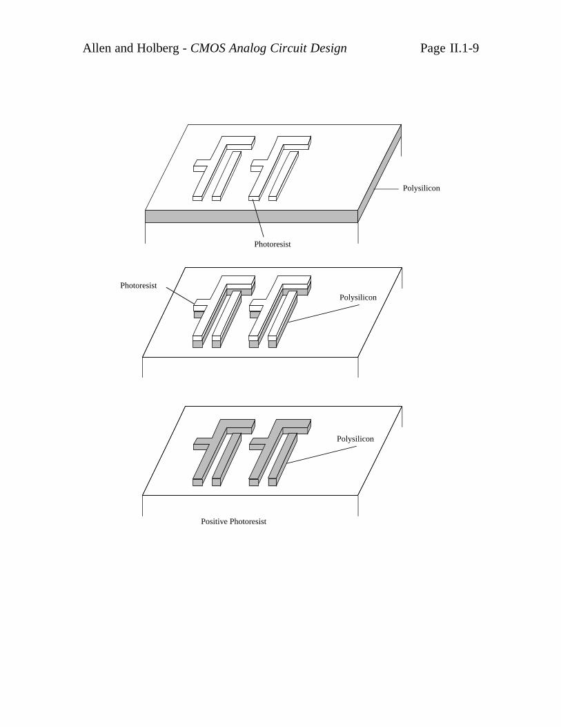
Allen and Holberg - CMOS Analog Circuit Design Page II.1-9
Positive Photoresist
Photoresist
Photoresist
Polysilicon
Polysilicon
Polysilicon
Allen and Holberg - CMOS Analog Circuit Design Page II.2-1
II.2 - CMOS TECHNOLOGY
TWIN-WELL CMOS TECHNOLOGY
Features
• Two layers of metal connections, both of them of high quality due to a
planarization step.
• Optimal threshold voltages of both p-channel and n-channel transistors
• Lightly doped drain (LDD) transistors prevent hot-electron effects.
• Good latchup protection
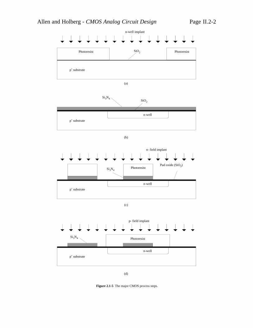
Allen and Holberg - CMOS Analog Circuit Design Page II.2-2
n-well implant
Photoresist Photoresist
(a)
Photoresist
p- field implant
Si3N4
(d)
n-well
(b)
Si3N4
n-well
PhotoresistPhotoresist
n- field implant
Pad oxide (SiO2)
(c)
n-well
Si3N4
Figure 2.1-5 The major CMOS process steps.
p- substrate
p- substrate
p- substrate
p- substrate
SiO2
SiO2
Allen and Holberg - CMOS Analog Circuit Design Page II.2-3
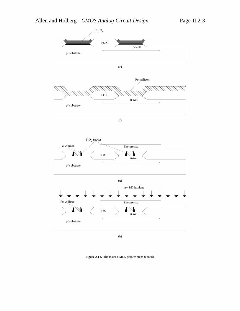
Photoresist
SiO2 spacer
Polysilicon
FOX
FOX
Polysilicon
n-well
FOX
(e)
(f)
(g)
n-well
n-well
Si3N4
Figure 2.1-5 The major CMOS process steps (cont'd).
p- substrate
p- substrate
p- substrate
FOX
FOX
FOX
Photoresist
n+ S/D implant
Polysilicon
FOX
(h)
n-well
p- substrate
FOX
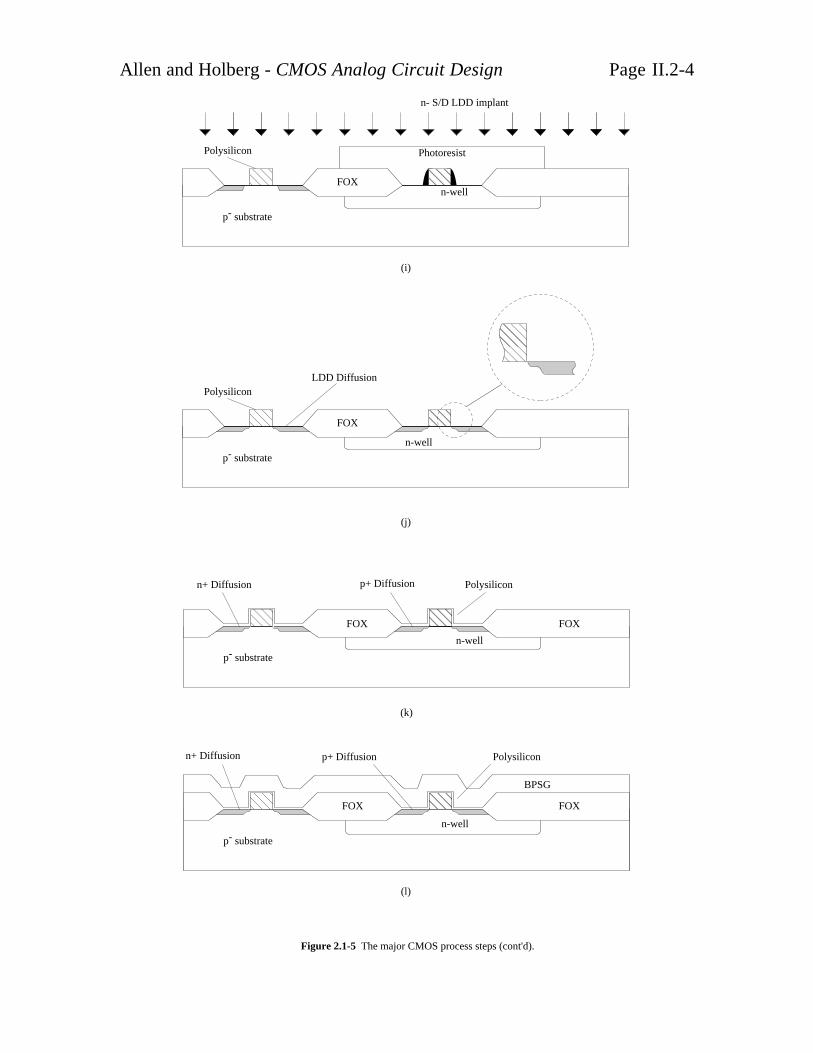
Allen and Holberg - CMOS Analog Circuit Design Page II.2-4
BPSG
Polysiliconn+ Diffusion p+ Diffusion
FOX FOX
(l)
Figure 2.1-5 The major CMOS process steps (cont'd).
n-well
Polysilicon
n-well
n+ Diffusion p+ Diffusion
FOX FOX
(k)
p- substrate
p- substrate
(j)
Photoresist
n- S/D LDD implant
Polysilicon
FOX
(i)
n-well
p- substrate
FOX
Polysilicon
FOX
n-well
p- substrate
FOX
LDD Diffusion
Allen and Holberg - CMOS Analog Circuit Design Page II.2-5
Figure 2.1-5 The major CMOS process steps (cont'd).
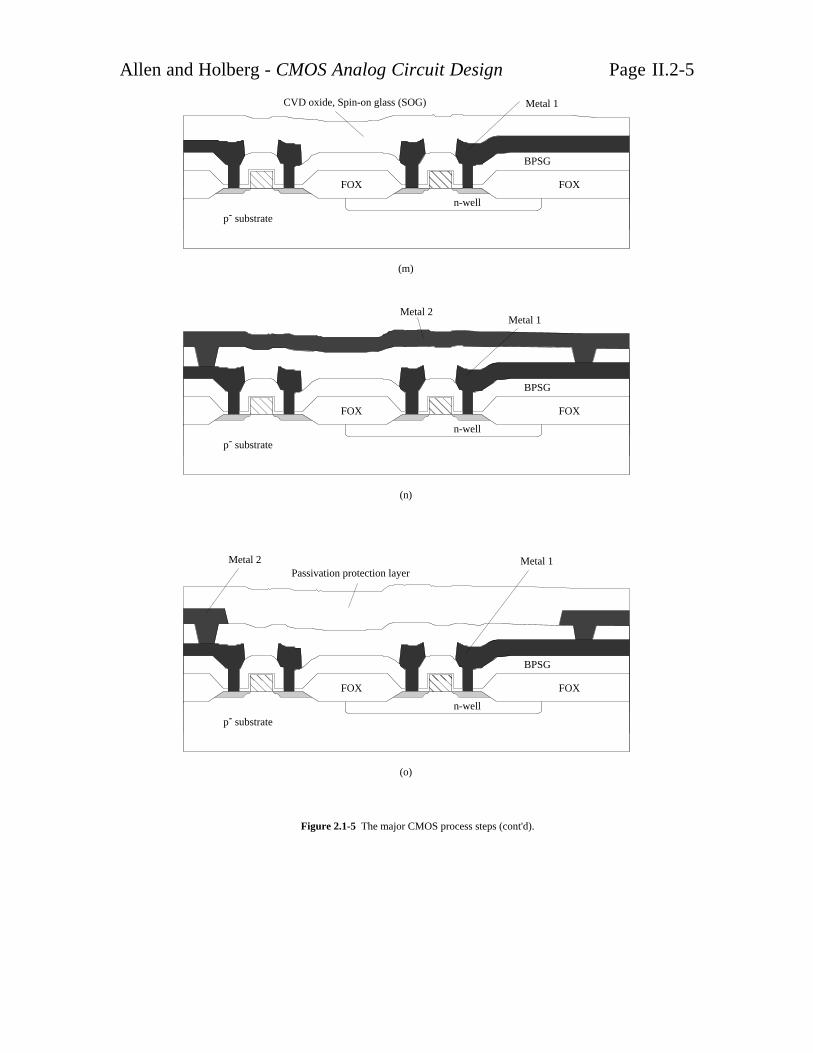
(m)
BPSG
n-well FOXFOX
p- substrate
BPSG
n-well
Metal 1
FOXFOX
p- substrate
(n)
(o)
Metal 2
BPSG
n-well
Metal 1
FOXFOX
p- substrate
Metal 2
Metal 1CVD oxide, Spin-on glass (SOG)
Passivation protection layer
Allen and Holberg - CMOS Analog Circuit Design Page II.2-6
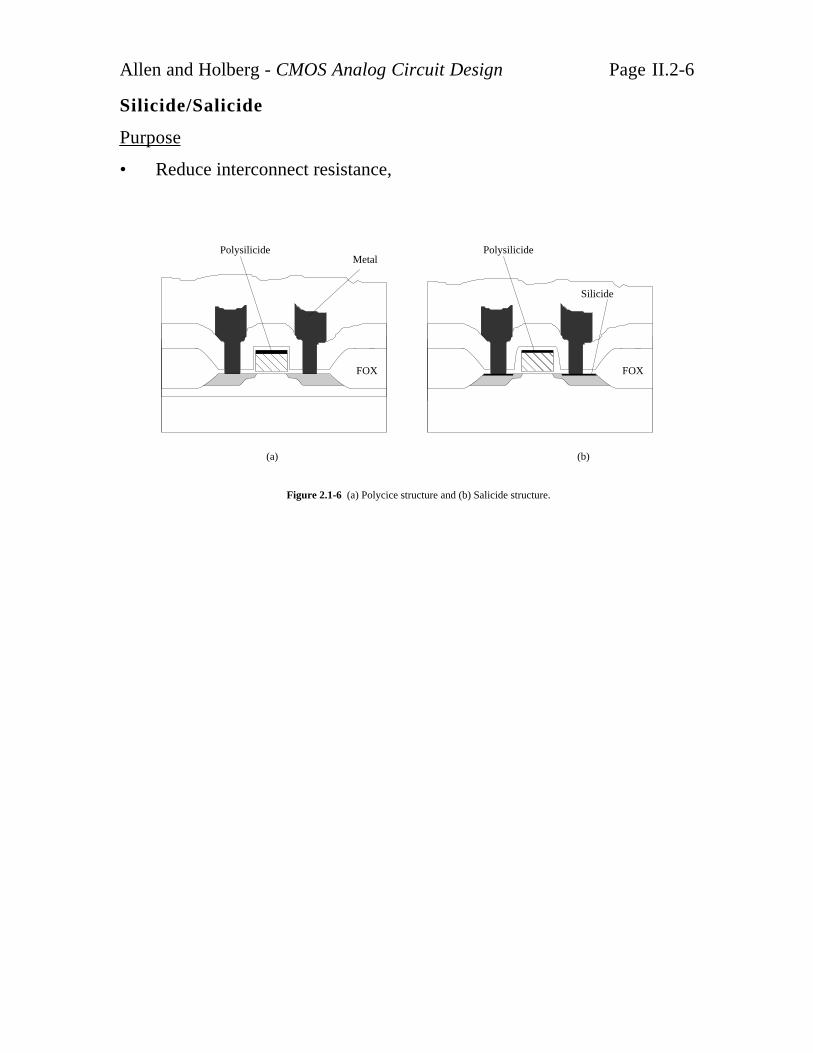
Silicide/Salicide
Purpose
• Reduce interconnect resistance,
Figure 2.1-6 (a) Polycice structure and (b) Salicide structure.
(a)
Metal
FOX
(b)
FOX
Polysilicide Polysilicide
Silicide
Allen and Holberg - CMOS Analog Circuit Design Page II.3-1
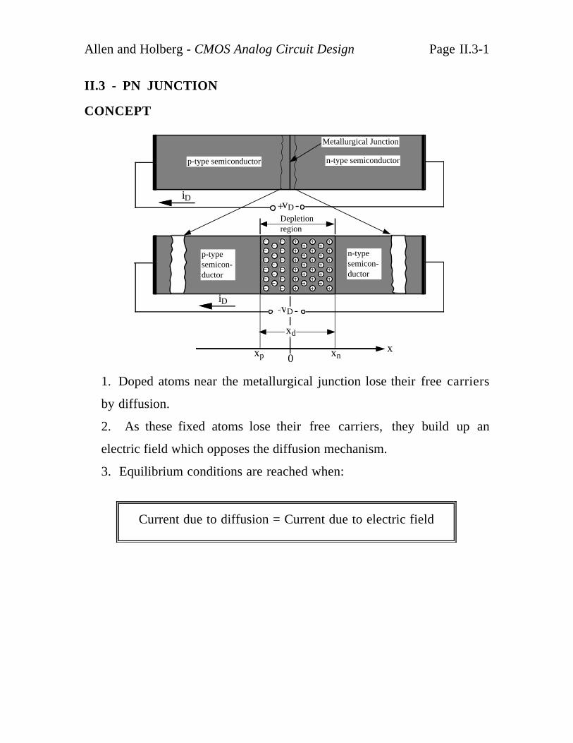
II.3 - PN JUNCTION
CONCEPT
Metallurgical Junction
p-type semiconductor n-type semiconductor
iD+ -vDDepletionregion
x
p-typesemicon-ductor
n-typesemicon-ductor
iD+ -vD
xd
xp xn0
1. Doped atoms near the metallurgical junction lose their free carriers
by diffusion.
2. As these fixed atoms lose their free carriers, they build up an
electric field which opposes the diffusion mechanism.
3. Equilibrium conditions are reached when:
Current due to diffusion = Current due to electric field
Allen and Holberg - CMOS Analog Circuit Design Page II.3-2
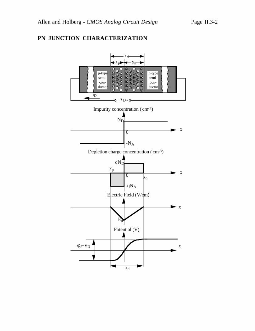
PN JUNCTION CHARACTERIZATION
ND
-NA
x0
Impurity concentration ( cm-3)
x0
Depletion charge concentration ( cm-3)
qND
-qNA
xp
xn
Electric Field (V/cm)
Eo
x
x
Potential (V)
xd
φ − vo D
p-typesemi-con-
ductor
n-typesemi-con-
ductor
iD+ -vD
xd
xnxp

Allen and Holberg - CMOS Analog Circuit Design Page II.3-3
SUMMARY OF PN JUNCTION ANALYSIS
Barrier potential-
φo = kTq ln
NAND
ni2 = Vt ln
NAND
ni2
Depletion region widths-
x n =
2εsi(φo-vD)NA
qND(NA+ND)
x p = 2εsi(φo-vD)ND
qND(NA+ND)
x ∝ 1N
Depletion capacitance-
Cj = AεsiqNAND
2(NA+ND) 1
φo-vD
= Cj0
φo-vD
Breakdown voltage-
BV = εsi(NA+ND)
2qNAND E
2max
Allen and Holberg - CMOS Analog Circuit Design Page II.3-4
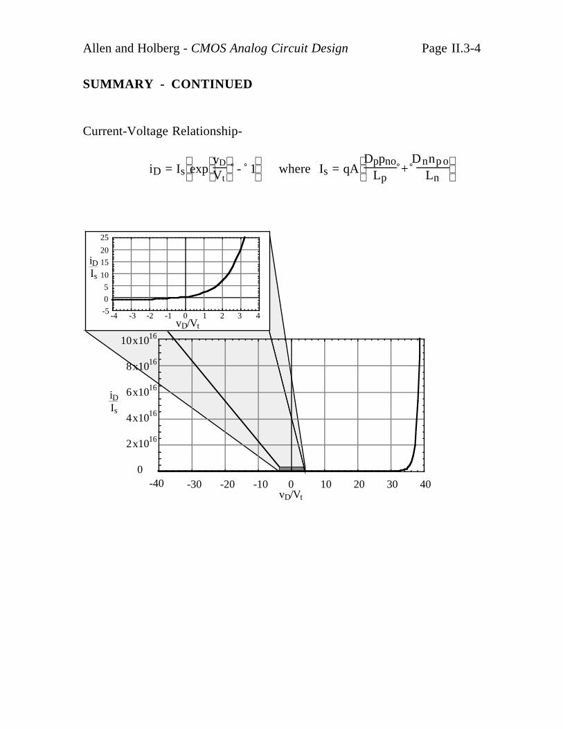
SUMMARY - CONTINUED
Current-Voltage Relationship-
iD = Is
exp
vD
Vt - 1 where Is = qA
Dppno
Lp +
Dnnp oLn
-40 -30 -20 -10 0 10 20 30 40vD/Vt
iDIs
10
8
6
4
2
0
x1016
x1016
x1016
x1016
x1016
-5
0
5
10
15
20
25
-4 -3 -2 -1 0 1 2 3 4
iDIs
vD/Vt
Allen and Holberg - CMOS Analog Circuit Design II.4-1
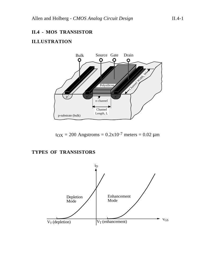
II.4 - MOS TRANSISTOR
ILLUSTRATION
Fig. 4.3-4n+ n+
p-substrate (bulk)
Channel Length, L
n-channel
Polysilicon
Bulk Source Gate Drain
p+
Chann
el W
idth,
W
tOX = 200 Angstroms = 0.2x10⁻⁷ meters = 0.02 µm
TYPES OF TRANSISTORS
vGS
iD
DepletionMode
EnhancementMode
VT (depletion) VT (enhancement)
Allen and Holberg - CMOS Analog Circuit Design II.4-2
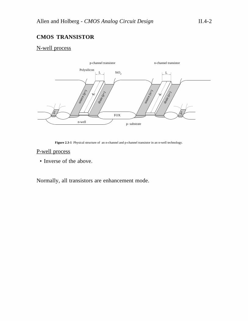
CMOS TRANSISTOR
N-well process
Figure 2.3-1 Physical structure of an n-channel and p-channel transistor in an n-well technology.
L
W
L
W
sour
ce (n
+)
drai
n (n
+)
sour
ce (p
+)
drai
n (p
+)
n-well
SiO2
Polysilicon
p- substrate
FOX
n+ p+
p-channel transistor n-channel transistor
P-well process
• Inverse of the above.
Normally, all transistors are enhancement mode.
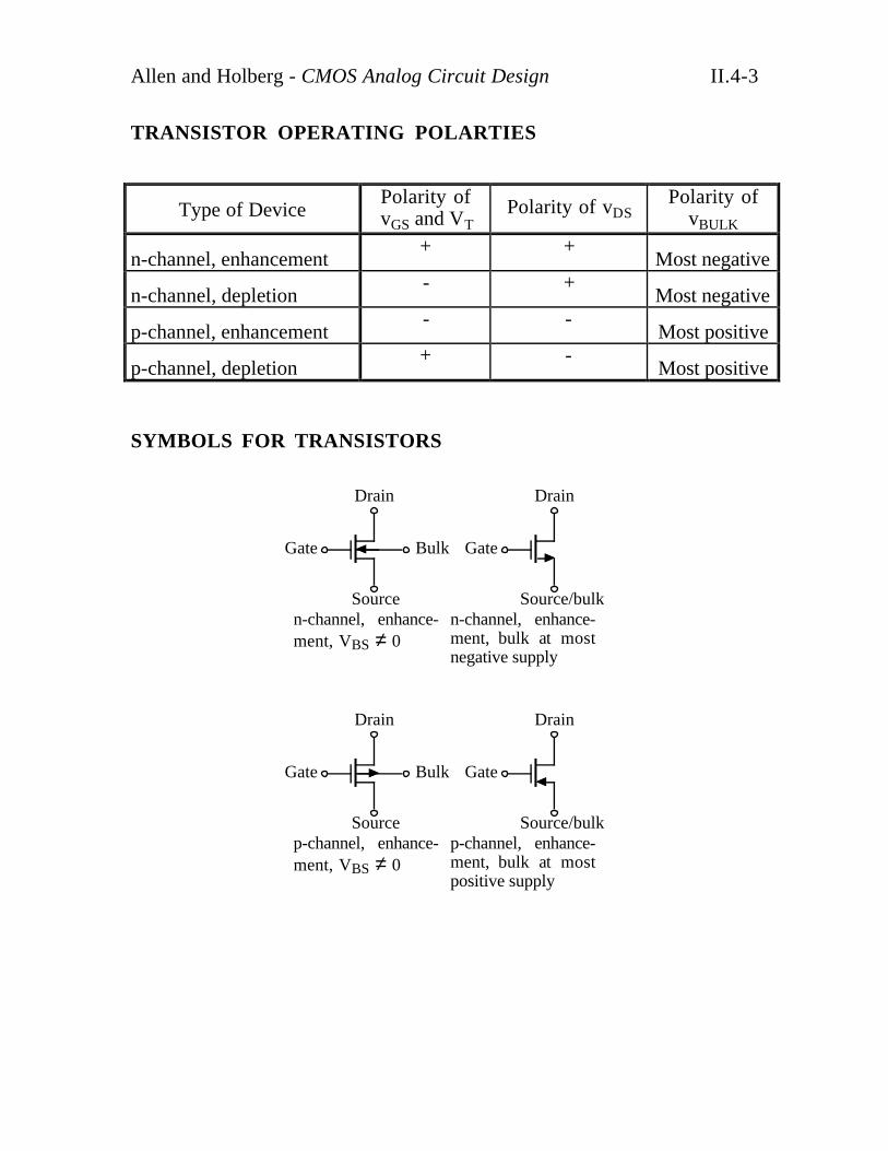
Allen and Holberg - CMOS Analog Circuit Design II.4-3
TRANSISTOR OPERATING POLARTIES
Type of DevicePolarity ofvGS and VT
Polarity of vDSPolarity of
vBULK
n-channel, enhancement+ +
Most negative
n-channel, depletion- +
Most negative
p-channel, enhancement- -
Most positive
p-channel, depletion+ -
Most positive
SYMBOLS FOR TRANSISTORS
Drain
Gate
Source/bulk
Drain
Gate
Source
Bulk
n-channel, enhance-ment, VBS ≠ 0
n-channel, enhance-ment, bulk at mostnegative supply
Drain
Gate
Source/bulk
Drain
Gate
Source
Bulk
p-channel, enhance-ment, VBS ≠ 0
p-channel, enhance-ment, bulk at mostpositive supply
Allen and Holberg - CMOS Analog Circuit Design II.5-1
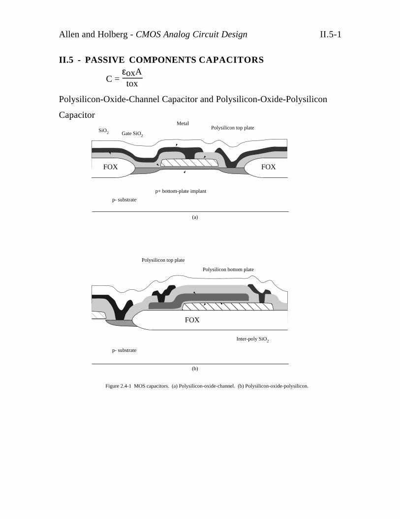
II.5 - PASSIVE COMPONENTS CAPACITORS
C = εoxAtox
Polysilicon-Oxide-Channel Capacitor and Polysilicon-Oxide-Polysilicon
Capacitor
p- substrate
p- substrate
FOX FOX
Figure 2.4-1 MOS capacitors. (a) Polysilicon-oxide-channel. (b) Polysilicon-oxide-polysilicon.
p+ bottom-plate implant
Polysilicon top plateGate SiO2
SiO2
Metal
FOX
Polysilicon top plate
Polysilicon bottom plate
Inter-poly SiO2
(a)
(b)
Allen and Holberg - CMOS Analog Circuit Design II.5-2
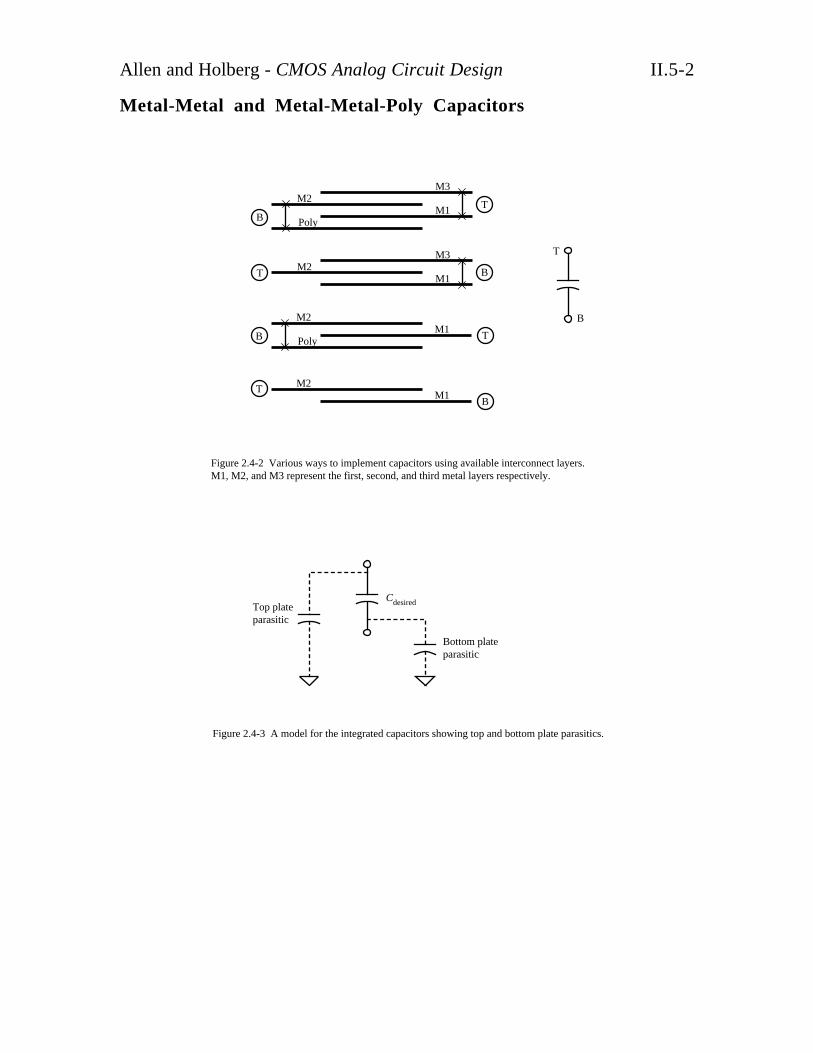
Metal-Metal and Metal-Metal-Poly Capacitors
CdesiredTop plate parasitic
Bottom plate parasitic
Figure 2.4-3 A model for the integrated capacitors showing top and bottom plate parasitics.
Figure 2.4-2 Various ways to implement capacitors using available interconnect layers. M1, M2, and M3 represent the first, second, and third metal layers respectively.
T
B
M3M2
M1T B
M3M2
M1PolyB
T
M2M1
PolyB T
M2M1
BT
Allen and Holberg - CMOS Analog Circuit Design II.5-3
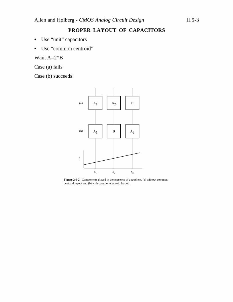
PROPER LAYOUT OF CAPACITORS
• Use “unit” capacitors
• Use “common centroid”
Want A=2*B
Case (a) fails
Case (b) succeeds!
Figure 2.6-2 Components placed in the presence of a gradient, (a) without common- centroid layout and (b) with common-centroid layout.
A1 A2 B
A1 B A2
(a)
(b)
x1 x2 x3
y
Allen and Holberg - CMOS Analog Circuit Design II.5-4
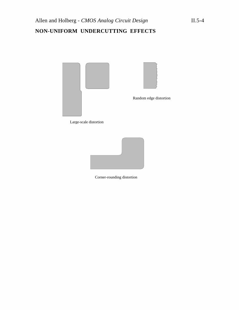
NON-UNIFORM UNDERCUTTING EFFECTS
Large-scale distortion
Random edge distortion
Corner-rounding distortion
Allen and Holberg - CMOS Analog Circuit Design II.5-5
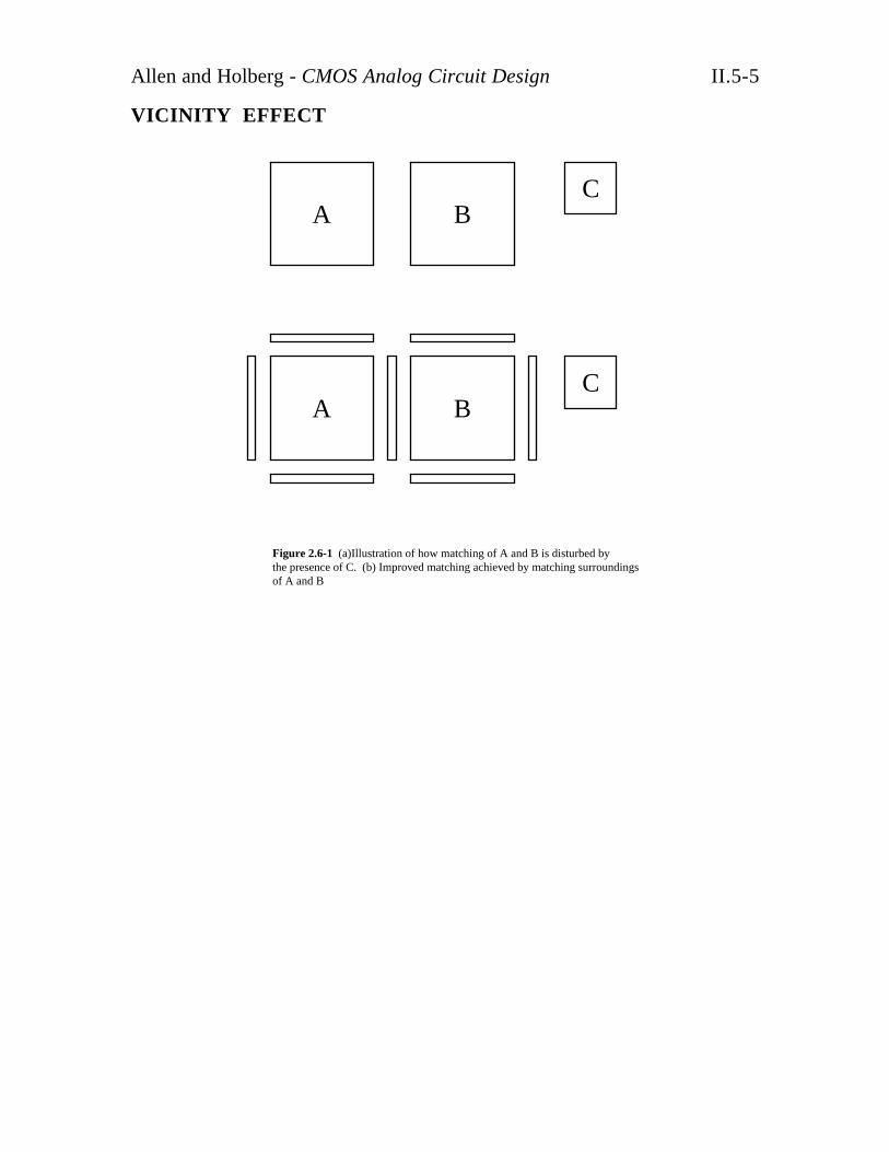
VICINITY EFFECT
Figure 2.6-1 (a)Illustration of how matching of A and B is disturbed by the presence of C. (b) Improved matching achieved by matching surroundings of A and B
A BC
A BC
Allen and Holberg - CMOS Analog Circuit Design II.5-6
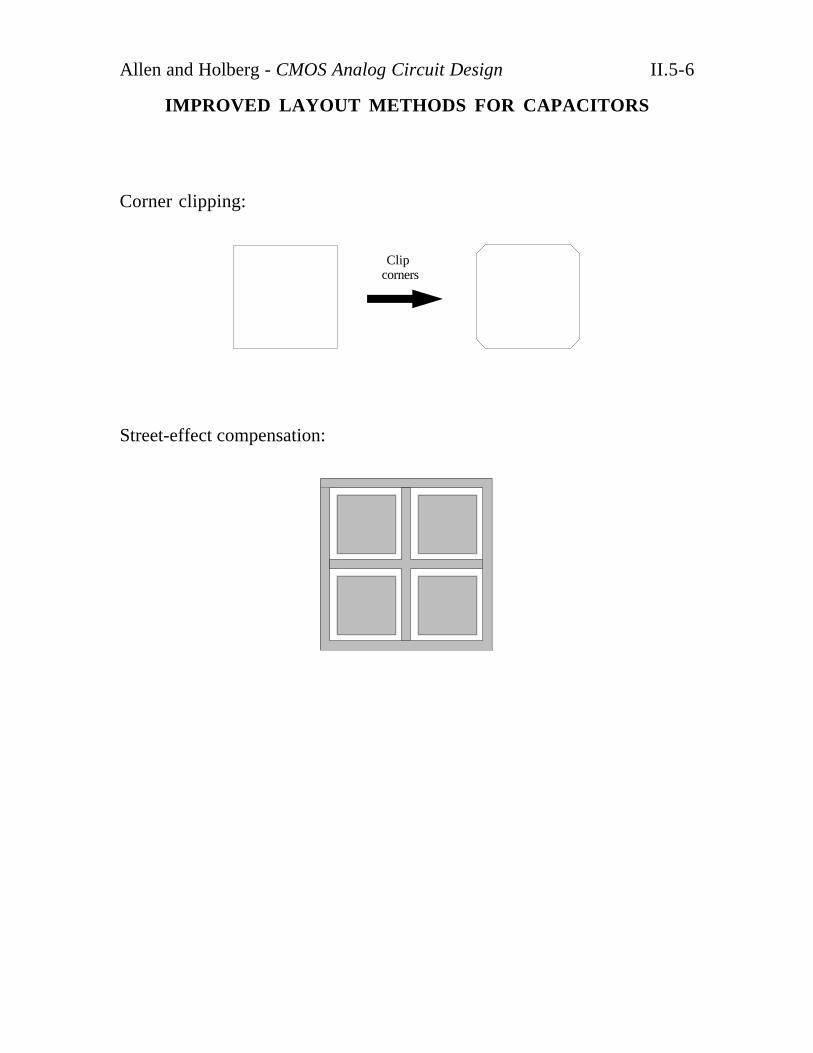
IMPROVED LAYOUT METHODS FOR CAPACITORS
Corner clipping:
Clip corners
Street-effect compensation:
Allen and Holberg - CMOS Analog Circuit Design II.5-7
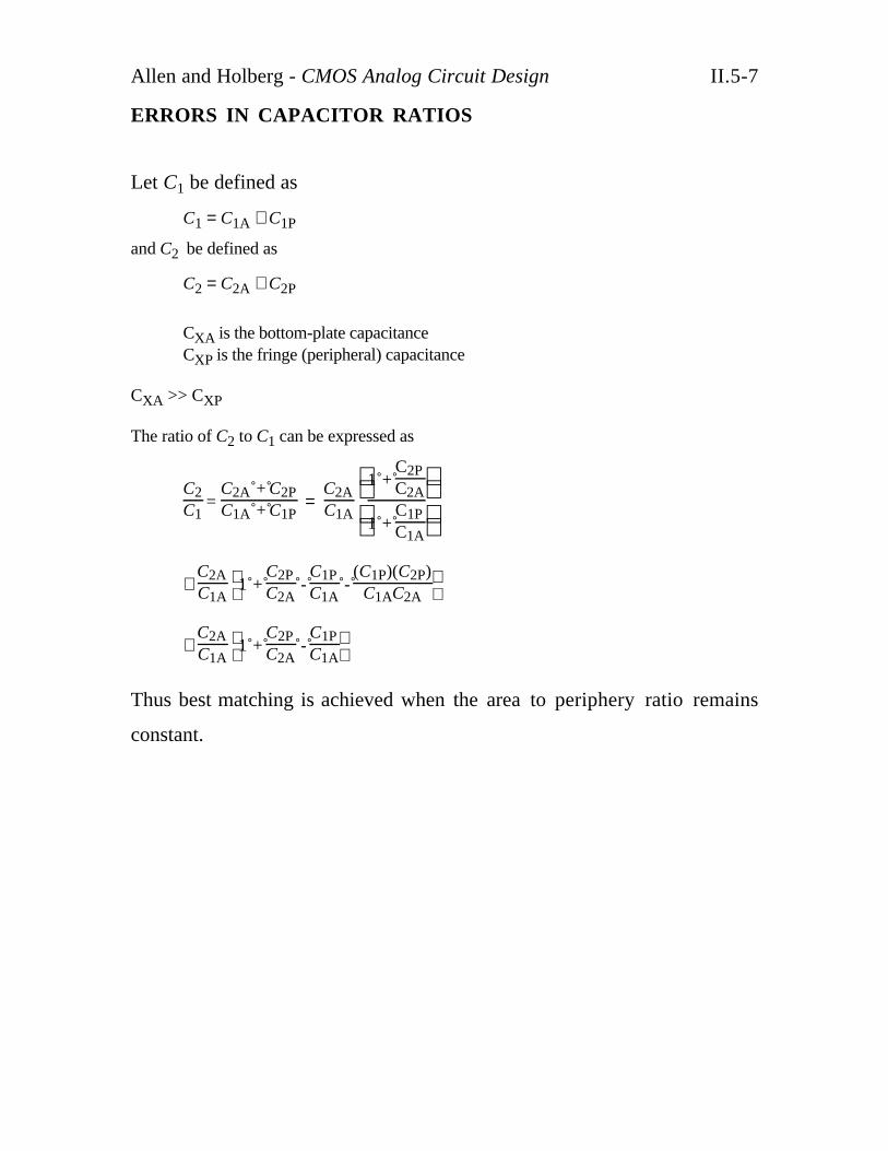
ERRORS IN CAPACITOR RATIOS
Let C1 be defined as
C1 = C1A + C1P
and C2 be defined as
C2 = C2A + C2P
CXA is the bottom-plate capacitanceCXP is the fringe (peripheral) capacitance
CXA >> CXP
The ratio of C2 to C1 can be expressed as
C2C1
= C2A + C2PC1A + C1P
= C2AC1A
1 +
C2PC2A
1 + C1PC1A
≅ C2AC1A
1 +
C2PC2A
- C1PC1A
- (C1P)(C2P)
C1AC2A
≅ C2AC1A
1 +
C2PC2A
- C1PC1A
Thus best matching is achieved when the area to periphery ratio remains
constant.
Allen and Holberg - CMOS Analog Circuit Design II.5-8
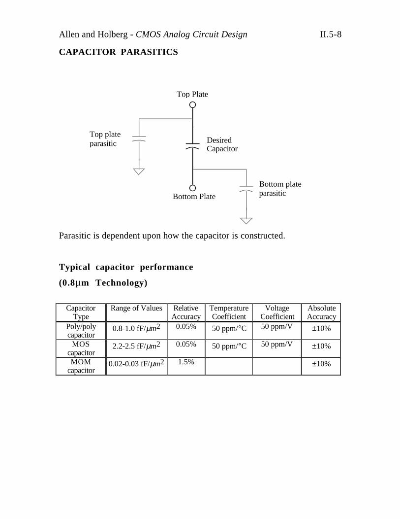
CAPACITOR PARASITICS
Top Plate
Bottom Plate
Top plateparasitic
Bottom plateparasitic
Desired Capacitor
Parasitic is dependent upon how the capacitor is constructed.
Typical capacitor performance
(0.8µm Technology)
CapacitorType
Range of Values RelativeAccuracy
TemperatureCoefficient
VoltageCoefficient
AbsoluteAccuracy
Poly/polycapacitor
0.8-1.0 fF/µm2 0.05% 50 ppm/°C 50 ppm/V ±10%
MOScapacitor
2.2-2.5 fF/µm2 0.05% 50 ppm/°C 50 ppm/V ±10%
MOMcapacitor
0.02-0.03 fF/µm2 1.5% ±10%
Allen and Holberg - CMOS Analog Circuit Design II.5-9
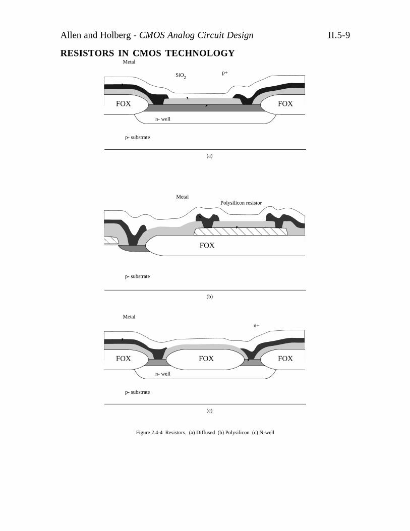
RESISTORS IN CMOS TECHNOLOGY
Figure 2.4-4 Resistors. (a) Diffused (b) Polysilicon (c) N-well
p- substrate
FOX FOX
SiO2
Metal
(a)
n- well
p+
p- substrate
FOX
(b)
Polysilicon resistorMetal
(c)
p- substrate
FOX FOX
Metal
n- well
n+
FOX
Allen and Holberg - CMOS Analog Circuit Design II.5-10
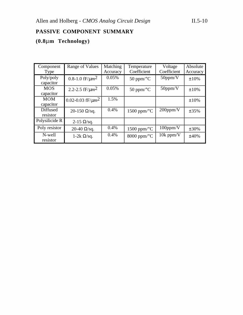
PASSIVE COMPONENT SUMMARY
(0.8µm Technology)
ComponentType
Range of Values MatchingAccuracy
TemperatureCoefficient
VoltageCoefficient
AbsoluteAccuracy
Poly/polycapacitor
0.8-1.0 fF/µm2 0.05% 50 ppm/°C 50ppm/V ±10%
MOScapacitor
2.2-2.5 fF/µm2 0.05% 50 ppm/°C 50ppm/V ±10%
MOMcapacitor
0.02-0.03 fF/µm2 1.5% ±10%
Diffusedresistor
20-150 Ω/sq. 0.4% 1500 ppm/°C 200ppm/V ±35%
Polysilicide R 2-15 Ω/sq.Poly resistor 20-40 Ω/sq. 0.4% 1500 ppm/°C 100ppm/V ±30%
N-wellresistor
1-2k Ω/sq. 0.4% 8000 ppm/°C 10k ppm/V ±40%
Allen and Holberg - CMOS Analog Circuit Design II.5-11
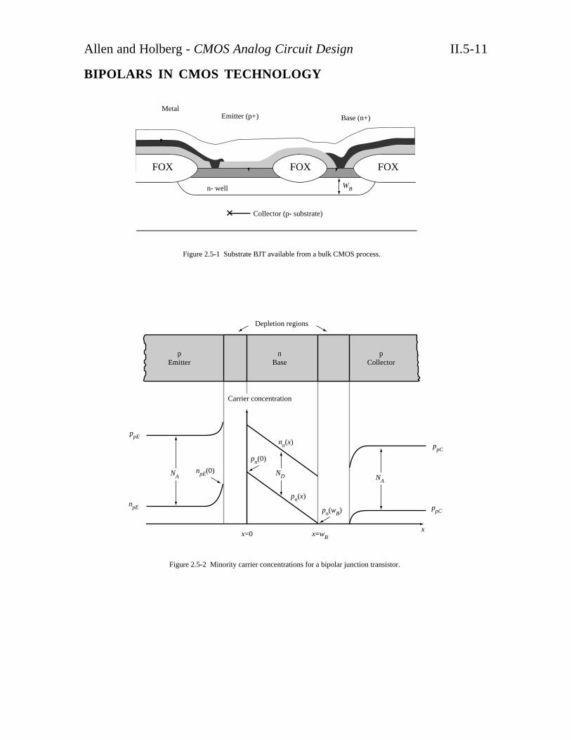
BIPOLARS IN CMOS TECHNOLOGY
Figure 2.5-1 Substrate BJT available from a bulk CMOS process.
Collector (p- substrate)
FOX FOX
Metal
n- well
Base (n+)
FOX
Emitter (p+)
NA NAND
Figure 2.5-2 Minority carrier concentrations for a bipolar junction transistor.
ppE
npE
ppC
ppC
nn(x)
pn(x)
pn(0)
pn(wB)
npE(0)
x=0 x=wBx
Carrier concentration
Depletion regions
WB
p Emitter
n Base
p Collector
Allen and Holberg - CMOS Analog Circuit Design II.6-1
II.6 - LATCHUP
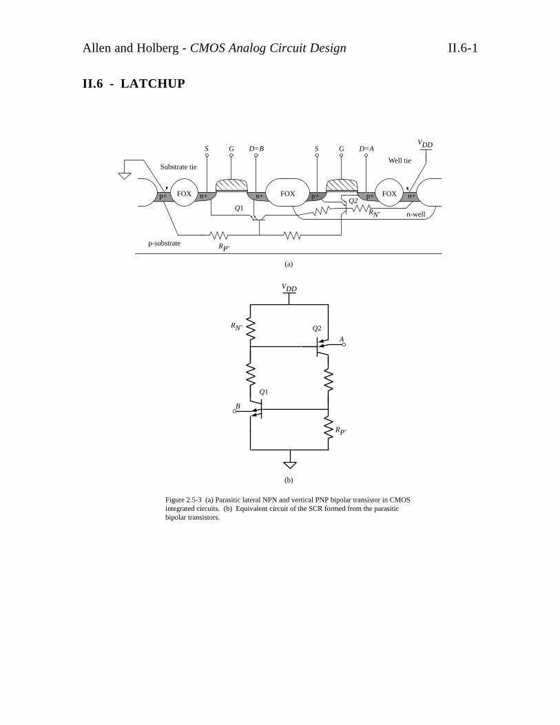
Figure 2.5-3 (a) Parasitic lateral NPN and vertical PNP bipolar transistor in CMOS integrated circuits. (b) Equivalent circuit of the SCR formed from the parasitic bipolar transistors.
(b)
VDD
RP-
RN-
B
A
Q1
Q2
G D=ASG D=BS
p-substrate
FOX FOX FOXn+ n+p+ p+ p+ n+
n-well
RP-
RN-Q1Q2
(a)
VDD
Substrate tieWell tie
Allen and Holberg - CMOS Analog Circuit Design II.6-2
PREVENTING LATCHUP
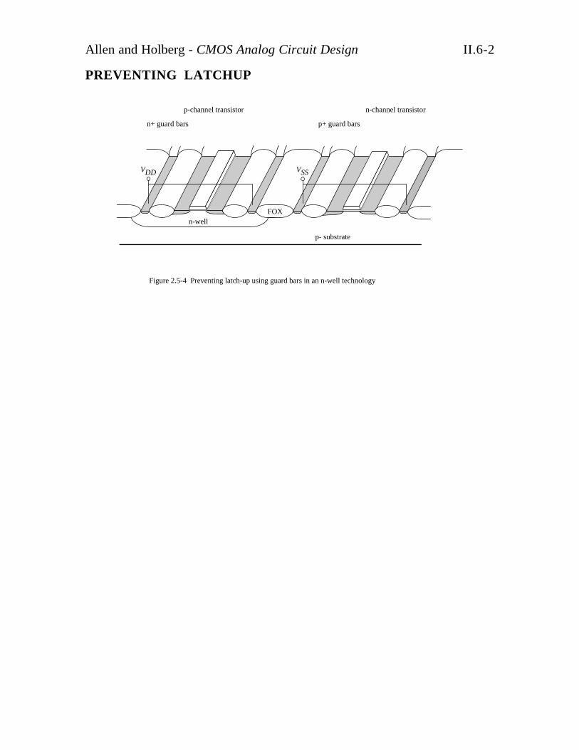
Figure 2.5-4 Preventing latch-up using guard bars in an n-well technology
n-well
p- substrate
FOX
n+ guard bars
n-channel transistor
p+ guard bars
p-channel transistor
VDD VSS
Allen and Holberg - CMOS Analog Circuit Design II.6-1
II.7 - ESD PROTECTION
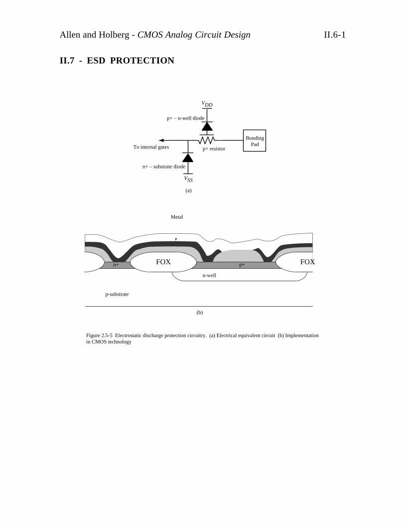
Figure 2.5-5 Electrostatic discharge protection circuitry. (a) Electrical equivalent circuit (b) Implementation in CMOS technology
p-substrate
FOX
Metal
n-well
FOXn+ p+
(a)
VDD
VSS
To internal gates
Bonding Pad
(b)
p+ – n-well diode
n+ – substrate diode
p+ resistor

Allen and Holberg - CMOS Analog Circuit Design II.8-1
II.8 - GEOMETRICAL CONSIDERATIONS
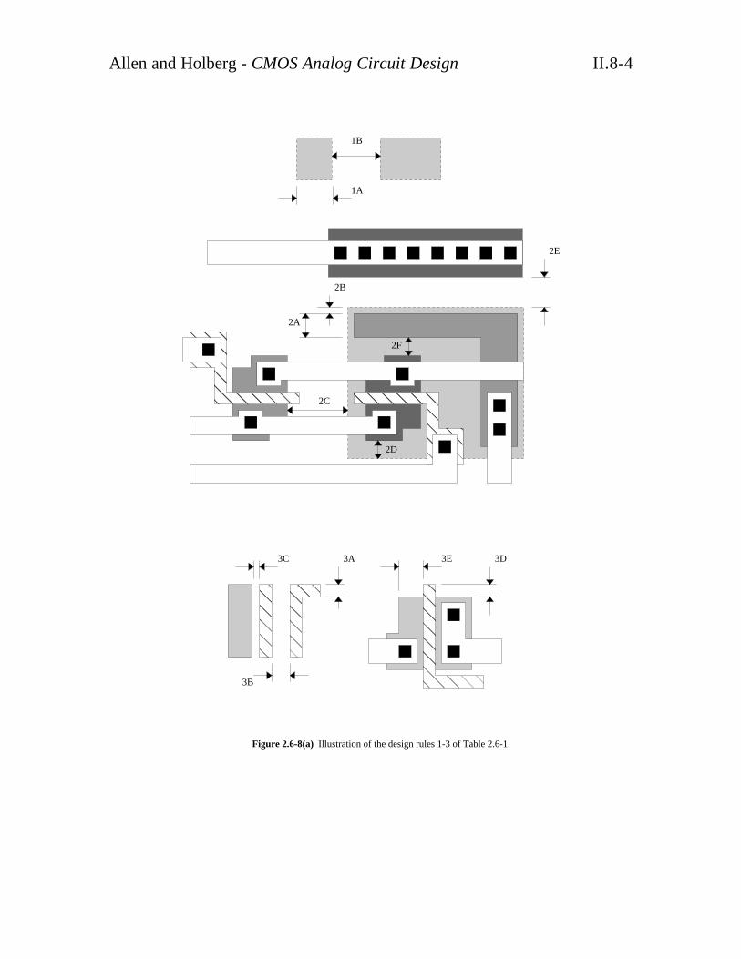
Design Rules for a Double-Metal, Double-Polysilicon, N-Well, Bulk CMOS Process.
Minimum Dimension Resolution (λ)
1. N-Well
1A. width .........................................................................6
1B. spacing .................................................................... 12
2. Active Area (AA)
2A. width .........................................................................4
Spacing to Well
2B. AA-n contained in n-Well.............................................1
2C. AA-n external to n-Well............................................. 10
2D. AA-p contained in n-Well.............................................3
2E. AA-p external to n-Well...............................................4
Spacing to other AA (inside or outside well)
2F. AA to AA (p or n).......................................................3
3. Polysilicon Gate (Capacitor bottom plate)
3A. width..........................................................................2
3B. spacing .......................................................................3
3C. spacing of polysilicon to AA (over field)........................1
3D. extension of gate beyond AA (transistor width dir.) ........2
3E. spacing of gate to edge of AA (transistor length dir.) ......4
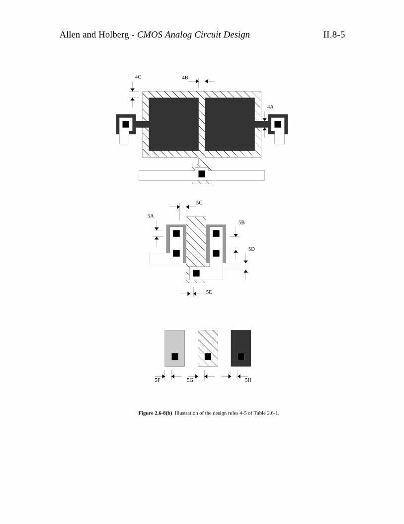
4. Polysilicon Capacitor top plate
4A. width..........................................................................2
4B. spacing .......................................................................2
4C. spacing to inside of polysilicon gate (bottom plate)..........2
5. Contacts

Allen and Holberg - CMOS Analog Circuit Design II.8-2
5A. size ....................................................................... 2x2
5B. spacing .......................................................................4
5C. spacing to polysilicon gate ............................................2
5D. spacing polysilicon contact to AA ..................................2
5E. metal overlap of contact ...............................................1
5F. AA overlap of contact ..................................................2
5G. polysilicon overlap of contact........................................2
5H. capacitor top plate overlap of contact.............................2
6. Metal-1
6A. width..........................................................................3
6B. spacing .......................................................................3
7. Via
7A. size ....................................................................... 3x3
7B. spacing .......................................................................4
7C. enclosure by Metal-1....................................................1
7D. enclosure by Metal-2....................................................1
8. Metal-2
8A. width..........................................................................4
8B. spacing .......................................................................3
Bonding Pad
8C. spacing to AA............................................................ 24
8D. spacing to metal circuitry ........................................... 24
8E. spacing to polysilicon gate .......................................... 24

Allen and Holberg - CMOS Analog Circuit Design II.8-3
9. Passivation Opening (Pad)
9A. bonding-pad opening ..............................100µm x 100µm
9B. bonding-pad opening enclosed by Metal-2 ......................8
9C. bonding-pad opening to pad opening space ................... 40
Note: For a P-Well process, exchange p and n in all instances.
Allen and Holberg - CMOS Analog Circuit Design II.8-4
1A
1B
3A
3B
3C 3D3E
2A
2B
2C
2D
2E
2F
Figure 2.6-8(a) Illustration of the design rules 1-3 of Table 2.6-1.
Allen and Holberg - CMOS Analog Circuit Design II.8-5
5F 5G 5H
5B
5D
5E
5A
5C
4C 4B
4A
Figure 2.6-8(b) Illustration of the design rules 4-5 of Table 2.6-1.
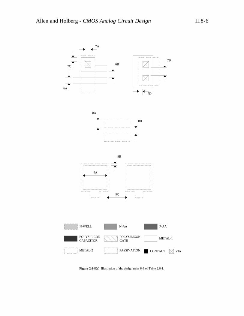
Allen and Holberg - CMOS Analog Circuit Design II.8-6
8B
8A
9B
9A
9C
N-WELL N-AA P-AA
POLYSILICON GATE
CONTACT VIA
METAL-1
METAL-2
POLYSILICON CAPACITOR
PASSIVATION
6B
6A
7C
7A
7D
7B
Figure 2.6-8(c) Illustration of the design rules 6-9 of Table 2.6-1.
Allen and Holberg - CMOS Analog Circuit Design II.8-7
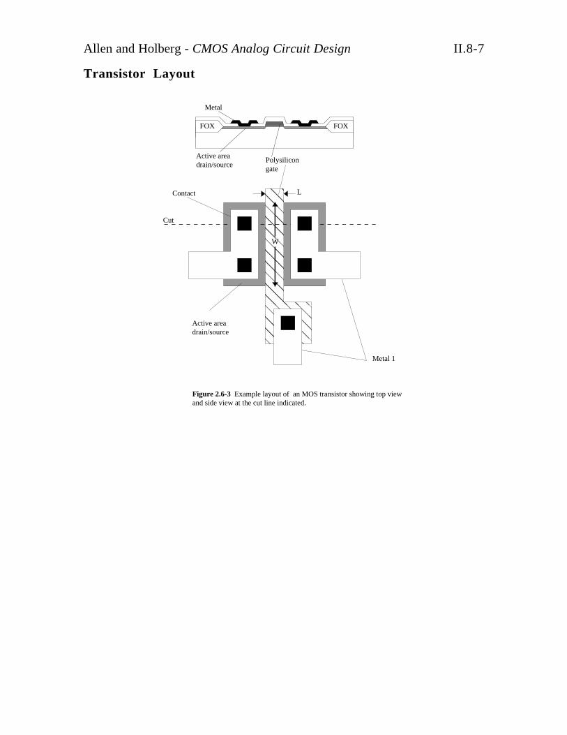
Transistor Layout
Figure 2.6-3 Example layout of an MOS transistor showing top view and side view at the cut line indicated.
Contact
Polysilicon gate
Active area drain/source
Metal 1
W
L
Cut
FOX FOX
Metal
Active area drain/source

Allen and Holberg - CMOS Analog Circuit Design II.8-8
SYMMETRIC VERSUS PHOTOLITHOGRAPHIC INVARIANT
Figure 2.6-4 Example layout of MOS transistors using (a) mirror symmetry, and (b) photolithographic invariance.
(a)
(b)
PLI IS BETTER
Allen and Holberg - CMOS Analog Circuit Design II.8-9
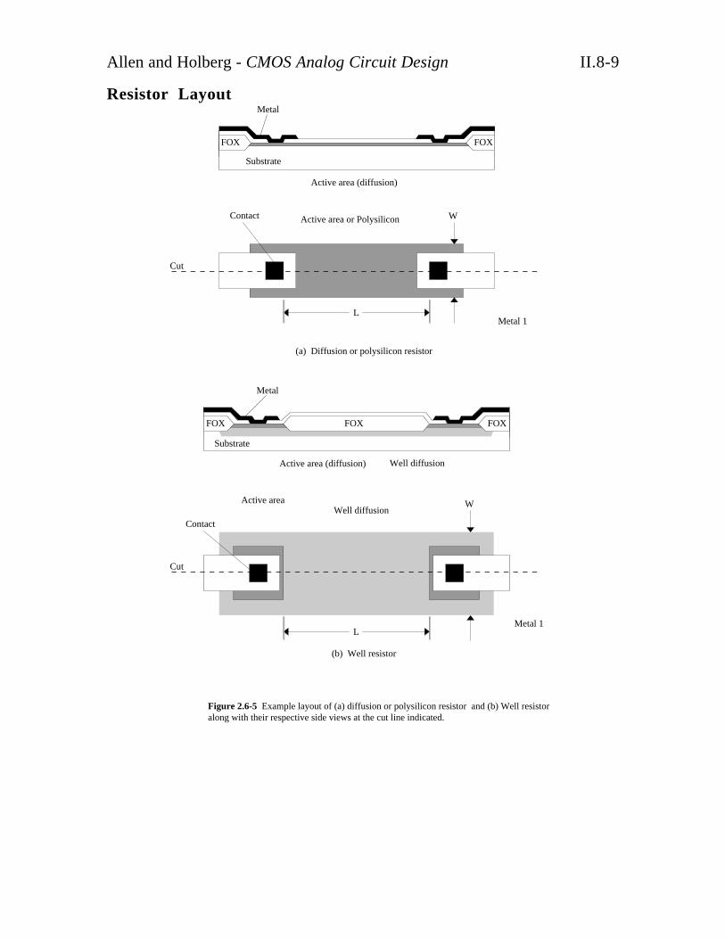
Resistor Layout
Figure 2.6-5 Example layout of (a) diffusion or polysilicon resistor and (b) Well resistor along with their respective side views at the cut line indicated.
Metal 1
Active area or PolysiliconContact
(a) Diffusion or polysilicon resistor
L
W
Metal 1
Well diffusion
Contact
(b) Well resistor
L
WActive area
FOX FOXFOX
Metal
Active area (diffusion)
FOX FOX
Metal
Active area (diffusion)
Well diffusion
Cut
Cut
Substrate
Substrate
Allen and Holberg - CMOS Analog Circuit Design II.8-10
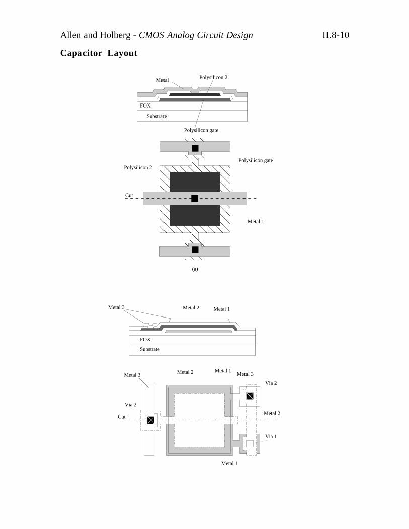
Capacitor Layout
Figure 2.6-7 Example layout of (a) double-polysilicon capacitor, and (b) triple-level metal capacitor along with their respective side views at the cut line indicated.
Polysilicon gate
FOX
Metal Polysilicon 2
Cut
Polysilicon gatePolysilicon 2
FOX
Metal 3 Metal 2 Metal 1
Metal 3 Metal 2 Metal 1Metal 3
Metal 2
Metal 1
Via 2
Via 2
Via 1
Cut
(a)
(b)
Metal 1
Substrate
Substrate
Allen and Holberg - CMOS Analog Circuit Design Page III.0-1
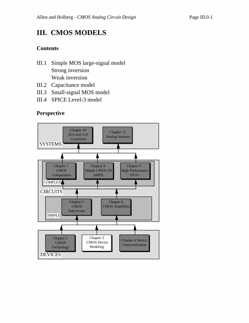
III. CMOS MODELS
Contents
III.1 Simple MOS large-signal modelStrong inversionWeak inversion
III.2 Capacitance modelIII.3 Small-signal MOS modelIII.4 SPICE Level-3 model
Perspective
DEVICES
SYSTEMS
CIRCUITS
Chapter 2 CMOS
Technology
Chapter 3 CMOS Device
Modeling
Chapter 4 Device Characterization
Chapter 7 CMOS
Comparators
Chapter 8 Simple CMOS OP
AMPS
Chapter 9 High Performance
OTA's
Chapter 5 CMOS
Subcircuits
Chapter 6 CMOS Amplifiers
Chapter 10D/A and A/D
Converters
Chapter 11Analog Systems
SIMPLE
COMPLEX
Allen and Holberg - CMOS Analog Circuit Design Page III.1-1
III.1 - MODELING OF CMOS ANALOG CIRCUITS
Objective
1. Hand calculations and design of analog CMOS circuits.2. Efficiently and accurately simulate analog CMOS circuits.
Large Signal Model
The large signal model is nonlinear and is used to solve for the dcvalues of the device currents given the device voltages.
The large signal models for SPICE:Basic drain current models -
1. Level 1 - Shichman-Hodges (VT, K', γ, λ, φ, and NSUB)
2. Level 2 - Geometry-based analytical model. Takes into accountsecond-order effects (varying channel charge, short-channel, weakinversion, varying surface mobility, etc.)
3. Level 3 - Semi-empirical short-channel model
4. Level 4 - BSIM model. Based on automatically generatedparameters from a process characterization. Good weak-stronginversion transition.
Basic model auxilliary parameters include capacitance [Meyer andWard-Dutton (charge-conservative)], bulk resistances, depletion regions,etc..
Small Signal Model
Based on the linearization of any of the above large signal models.
Simulator Software
SPICE2 - Generic SPICE available from UC Berkeley (FORTRAN)
SPICE3 - Generic SPICE available from UC Berkeley (C)
*SPICE*- Every other SPICE simulator!

Allen and Holberg - CMOS Analog Circuit Design Page III.1-2
Transconductance Characteristics of NMOS when VDS = 0.1V
vGS ≤ VT:
vGS
iD
VT 3VT2VT
00
vGS = VT
+
-VDS
=0.1V
+
-
p substrate (bulk)
Gate Drain
iDSource
andbulk
vGS = 2VT:
vGS
iD
VT 3VT2VT
00
VDS=0.1V
+
-
+
-vGS = 2VT
p substrate (bulk)
Gate Drain
iDSource
andbulk
vGS = 3VT:
vGS
iD
VT 3VT2VT
00
vGS = 3VT
+
-VDS
=0.1V
+
-
p substrate (bulk)
Gate Drain
iDSource
andbulk
Allen and Holberg - CMOS Analog Circuit Design Page III.1-3
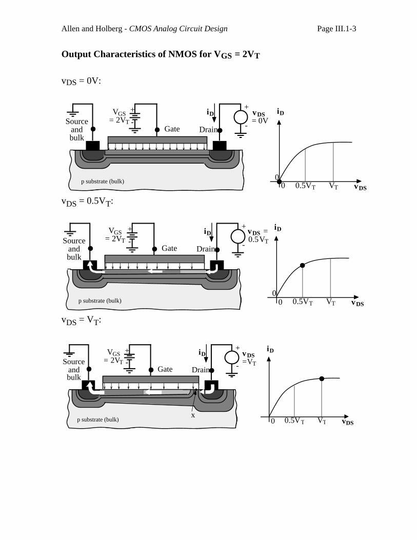
Output Characteristics of NMOS for VGS = 2VT
vDS = 0V:
vDS = 0V
p substrate (bulk)
Gate Drain
+
-
iD+
-Sourceandbulk
VGS= 2VT
iD
vDS
00 VT0.5VT
vDS = 0.5VT:
p substrate (bulk)
Gate Drain
+
-
iD+
-Sourceandbulk
vDS =0.5VT
VGS= 2VT
iD
vDS
00 VT0.5VT
vDS = VT:
iD
vDS0 VT0.5VTp substrate (bulk)
Gate Drain
+
-
iD+
-Sourceandbulk
vDS=VT
x
VGS= 2VT
Allen and Holberg - CMOS Analog Circuit Design Page III.1-4
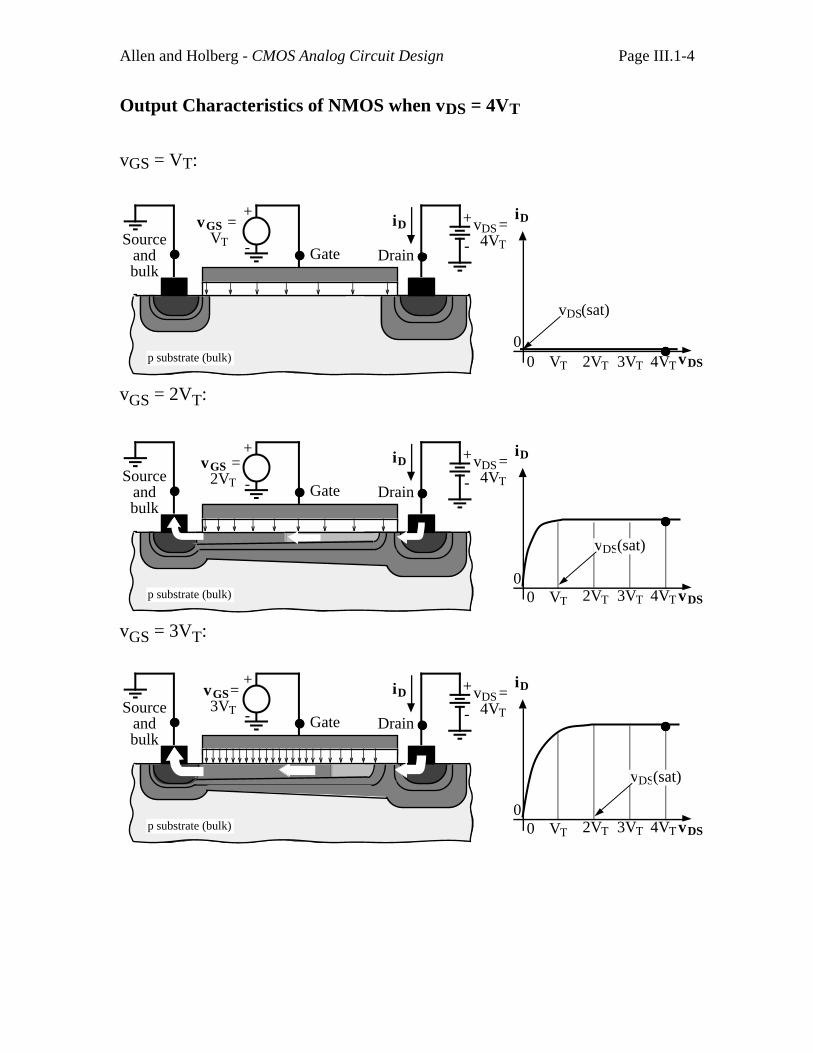
Output Characteristics of NMOS when vDS = 4VT
vGS = VT:
iD
VT vDS
00 2VT 4VT3VT
vDS(sat)
p substrate (bulk)
Gate Drain
+
-
iD+
-Sourceandbulk
vDS = 4VT
vGS = VT
vGS = 2VT:
iD
VT vDS
00 2VT 4VT3VT
vDS(sat)
p substrate (bulk)
Gate Drain
+
-
iD+
-Sourceandbulk
vGS = 2VT
vDS = 4VT
vGS = 3VT:
iD
VT vDS
00 2VT 4VT3VT
vDS(sat)
vDS = 4VT
p substrate (bulk)
Gate Drain
+
-
iD+
-Sourceandbulk
vGS= 3VT
Allen and Holberg - CMOS Analog Circuit Design Page III.1-5
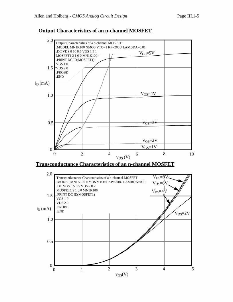
Output Characteristics of an n-channel MOSFET
Transconductance Characteristics of an n-channel MOSFETvDS (V)
0 2 4 6 8 100
iD (mA)
VGS=1V
VGS=2V
VGS=3V
VGS=4V
VGS=5V
0.5
1.0
1.5
2.0Output Characteristics of a n-channel MOSFET.MODEL MN1K100 NMOS VTO=1 KP=200U LAMBDA=0.01.DC VDS 0 10 0.5 VGS 1 5 1MOSFET1 2 1 0 0 MN1K100.PRINT DC ID(MOSFET1)VGS 1 0 VDS 2 0 .PROBE.END
0
iD (mA)
0 1vGS(V)
VDS=8VVDS=6V
VDS=2V
2 3 4 5
0.5
1.0
1.5
2.0
VDS=4V
Transconductance Characteristics of a n-channel MOSFET.MODEL MN1K100 NMOS VTO=1 KP=200U LAMBDA=0.01.DC VGS 0 5 0.5 VDS 2 8 2MOSFET1 2 1 0 0 MN1K100.PRINT DC ID(MOSFET1)VGS 1 0 VDS 2 0 .PROBE.END
Allen and Holberg - CMOS Analog Circuit Design Page III.1-6
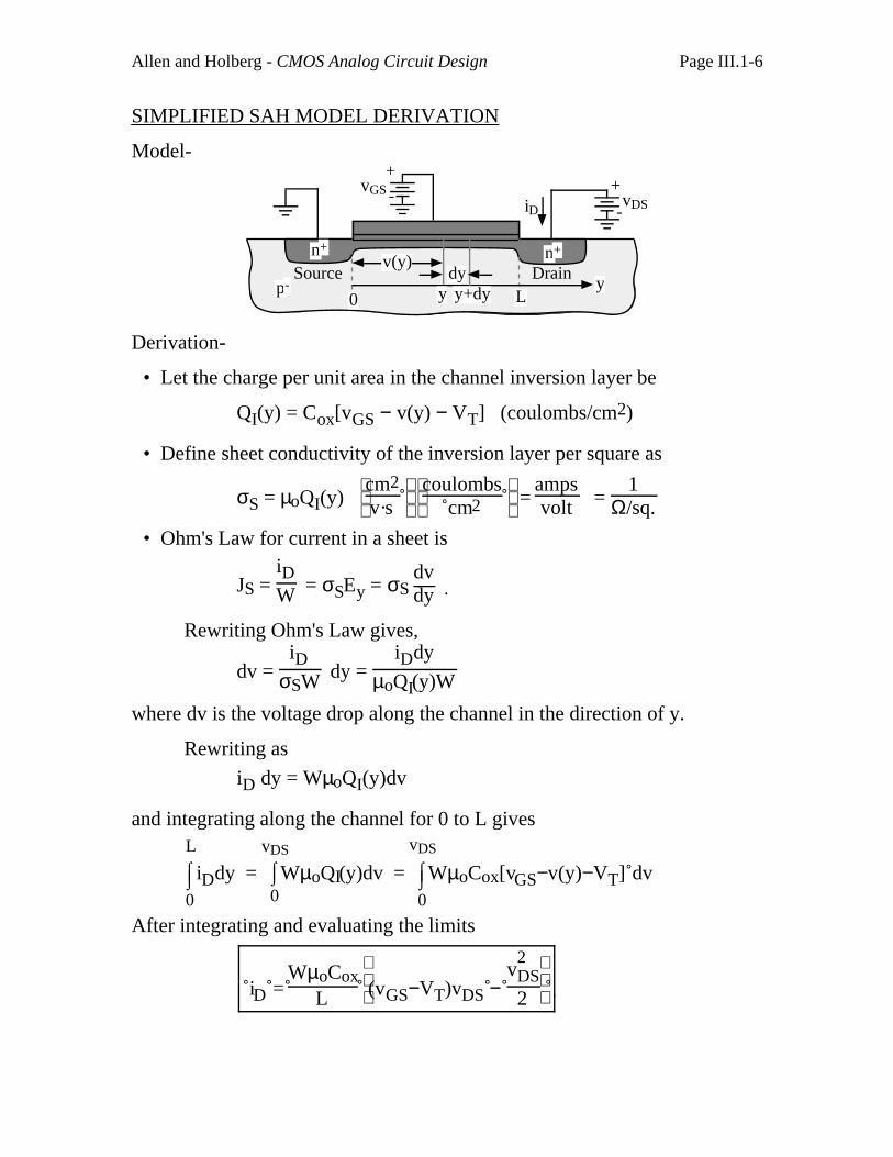
SIMPLIFIED SAH MODEL DERIVATION
Model-
n+ n+
yv(y)
dy
0 Ly y+dyp-Source Drain
+
-vGS
-iD+
vDS
Derivation-
• Let the charge per unit area in the channel inversion layer be
QI(y) = Cox[vGS − v(y) − VT] (coulombs/cm2)
• Define sheet conductivity of the inversion layer per square as
σS = µoQI(y)
cm2
v·s
coulombs
cm2 = ampsvolt =
1Ω/sq.
• Ohm's Law for current in a sheet is
JS = iDW = σSEy = σS
dvdy .
Rewriting Ohm's Law gives,
dv = iD
σSW dy = iDdy
µoQI(y)W
where dv is the voltage drop along the channel in the direction of y.
Rewriting as
iD dy = WµoQI(y)dv
and integrating along the channel for 0 to L gives
⌡⌠
0
L
iDdy = ⌡⌠0
vDS
WµoQI(y)dv = ⌡⌠
0
vDS
WµoCox[vGS−v(y)−VT] dv
After integrating and evaluating the limits
iD = WµoCox
L
(vGS−VT)vDS − v
2DS2
Allen and Holberg - CMOS Analog Circuit Design Page III.1-7
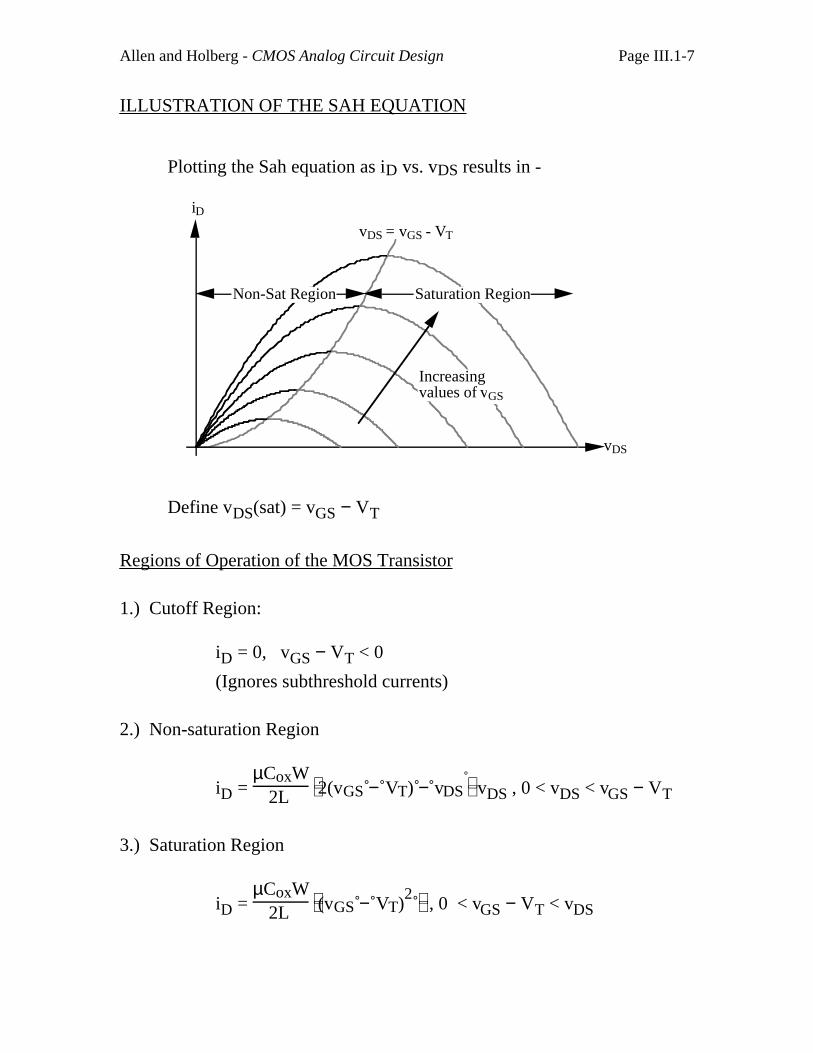
ILLUSTRATION OF THE SAH EQUATION
Plotting the Sah equation as iD vs. vDS results in -
iDvDS = vGS - VT
Increasingvalues of vGS
Saturation RegionNon-Sat Region
vDS
Define vDS(sat) = vGS − VT
Regions of Operation of the MOS Transistor
1.) Cutoff Region:
iD = 0, vGS − VT < 0
(Ignores subthreshold currents)
2.) Non-saturation Region
iD = µCoxW
2L 2(vGS − VT) − vDS vDS , 0 < vDS < vGS − VT
3.) Saturation Region
iD = µCoxW
2L (vGS − VT)2 , 0 < vGS − VT < vDS
Allen and Holberg - CMOS Analog Circuit Design Page III.1-8
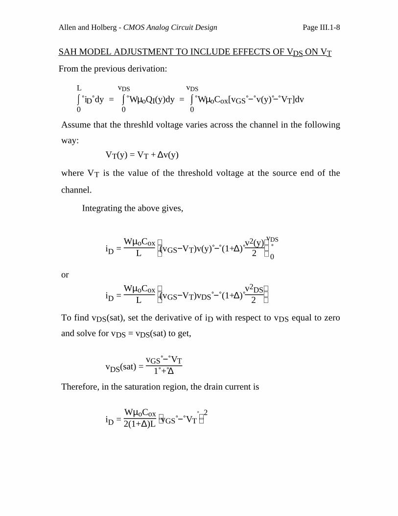
SAH MODEL ADJUSTMENT TO INCLUDE EFFECTS OF V DS ON V T
From the previous derivation:
⌡⌠0
L
iD dy = ⌡⌠0
vDS
WµoQI(y)dy = ⌡⌠0
vDS
WµoCox[vGS − v(y) − VT]dv
Assume that the threshld voltage varies across the channel in the following
way:
VT(y) = VT + ∆v(y)
where VT is the value of the threshold voltage at the source end of the
channel.
Integrating the above gives,
iD = WµoCox
L
(vGS−VT)v(y) − (1+∆) v2(y)
2
vDS
0
or
iD = WµoCox
L
(vGS−VT)vDS − (1+∆) v2DS
2
To find vDS(sat), set the derivative of iD with respect to vDS equal to zero
and solve for vDS = vDS(sat) to get,
vDS(sat) = vGS − VT
1 + ∆
Therefore, in the saturation region, the drain current is
iD = WµoCox2(1+∆)L vGS − VT
2
Allen and Holberg - CMOS Analog Circuit Design Page III.1-9
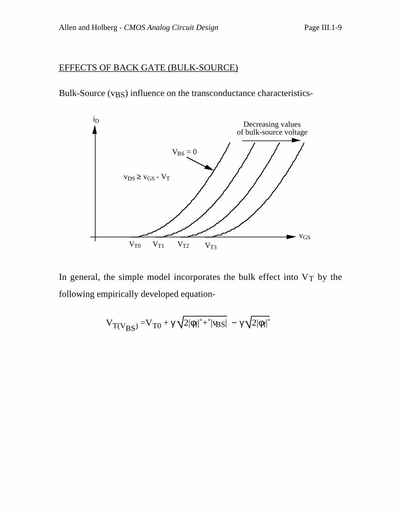
EFFECTS OF BACK GATE (BULK-SOURCE)
Bulk-Source (vBS) influence on the transconductance characteristics-
vGS
iD Decreasing valuesof bulk-source voltage
VT0 VT1 VT2 VT3
VBS = 0
vDS ≥ vGS - VT
In general, the simple model incorporates the bulk effect into VT by the
following empirically developed equation-
VT(VBS) =VT0 + γ 2|φf| + |vBS| − γ 2|φf|
Allen and Holberg - CMOS Analog Circuit Design Page III.1-10
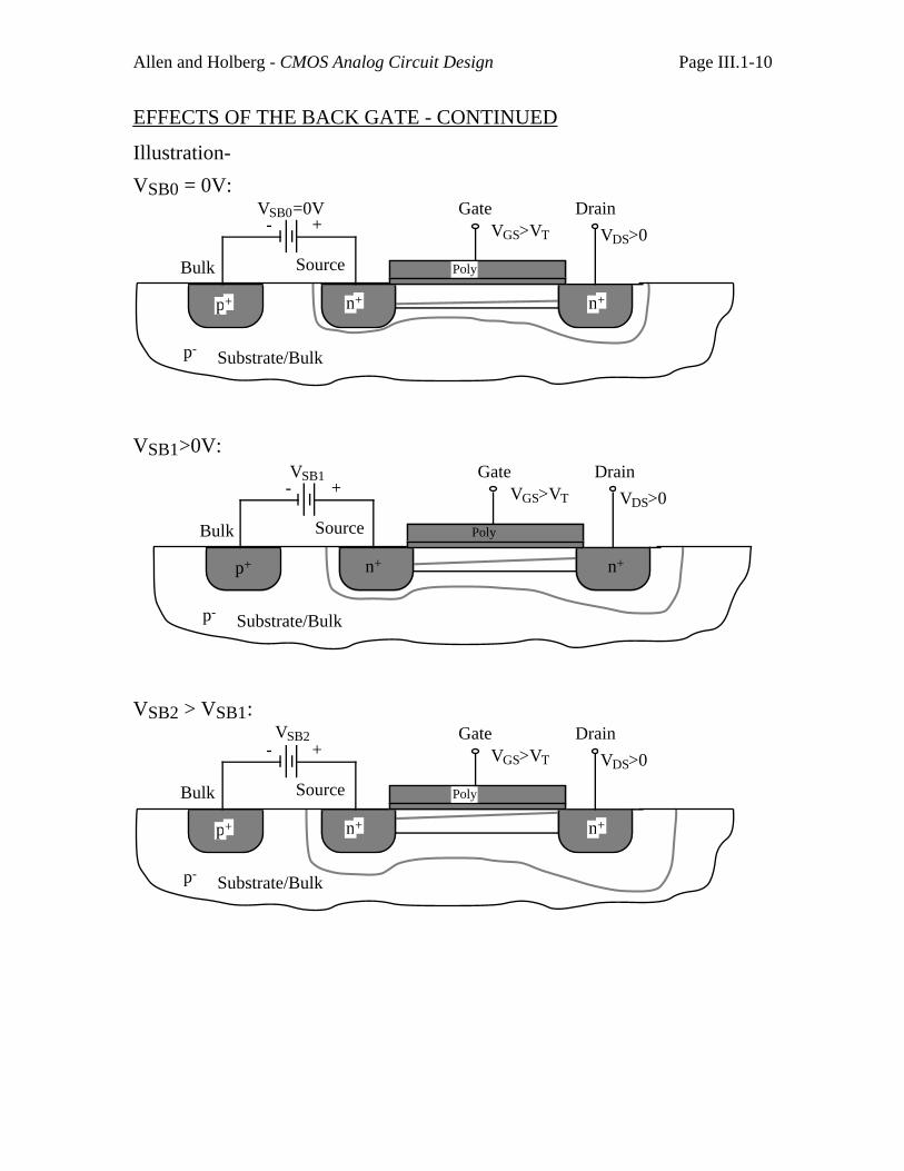
EFFECTS OF THE BACK GATE - CONTINUED
Illustration-
VSB0 = 0V:
Poly
p+ n+ n+
p-
+-
Bulk Source
Gate Drain
VDS>0VGS>VT
Substrate/Bulk
VSB0=0V
VSB1>0V:
Poly
p+ n+ n+
p-
+-
Bulk Source
Gate Drain
VDS>0VGS>VT
Substrate/Bulk
VSB1
VSB2 > VSB1:
Poly
p+ n+ n+
p-
+-
Bulk Source
Gate Drain
VDS>0VGS>VT
Substrate/Bulk
VSB2
Allen and Holberg - CMOS Analog Circuit Design Page III.1-11
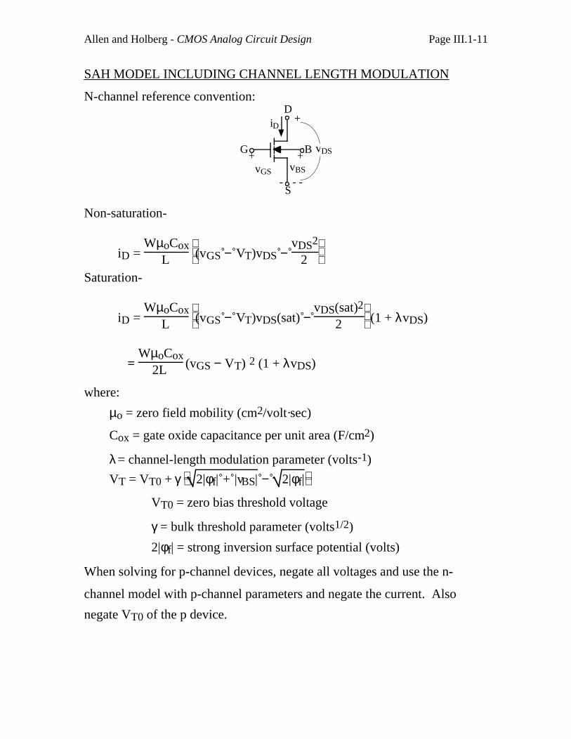
SAH MODEL INCLUDING CHANNEL LENGTH MODULATION
N-channel reference convention:
+
+
- -
+
-vBS
vDS
vGS
iD
D
B
S
G
Non-saturation-
iD = WµoCox
L
(vGS − VT)vDS − vDS2
2
Saturation-
iD = WµoCox
L
(vGS − VT)vDS(sat) − vDS(sat)2
2 (1 + λvDS)
= WµoCox
2L (vGS − VT) 2 (1 + λvDS)
where:
µo = zero field mobility (cm2/volt·sec)
Cox = gate oxide capacitance per unit area (F/cm2)
λ = channel-length modulation parameter (volts-1)
VT = VT0 + γ 2|φf| + |vBS| − 2|φf|
VT0 = zero bias threshold voltage
γ = bulk threshold parameter (volts1/2)
2|φf| = strong inversion surface potential (volts)
When solving for p-channel devices, negate all voltages and use the n-
channel model with p-channel parameters and negate the current. Also
negate VT0 of the p device.
Allen and Holberg - CMOS Analog Circuit Design Page III.1-12
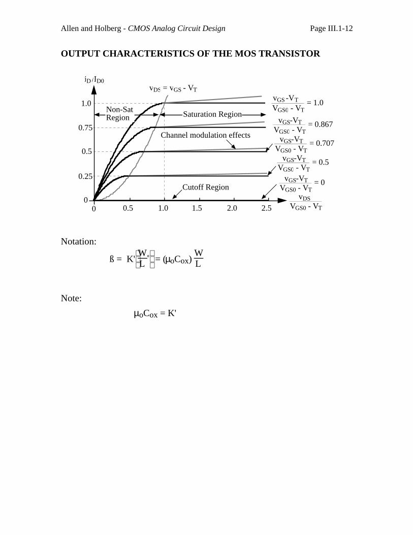
OUTPUT CHARACTERISTICS OF THE MOS TRANSISTOR
-VTvGS
vDS - VT
iD /ID0
0.75
1.0
0.5
0.25
00 0.5 1.0 1.5 2.0 2.5
vGS-VT - VT
= 0
vGS-VTVGS0 - VT
= 0.5
vGS-VT - VT
= 0.707
vGS-VTVGS0 - VT
= 0.867
VGS0 - VT = 1.0
Channel modulation effects
vDSVGS0 - VT
Non-SatRegion Saturation Region
Cutoff Region VGS0
VGS0
= vGS
Notation:
ß = K'
W
L = (µoCox) WL
Note:
µoCox = K'
Allen and Holberg - CMOS Analog Circuit Design Page III.1-13
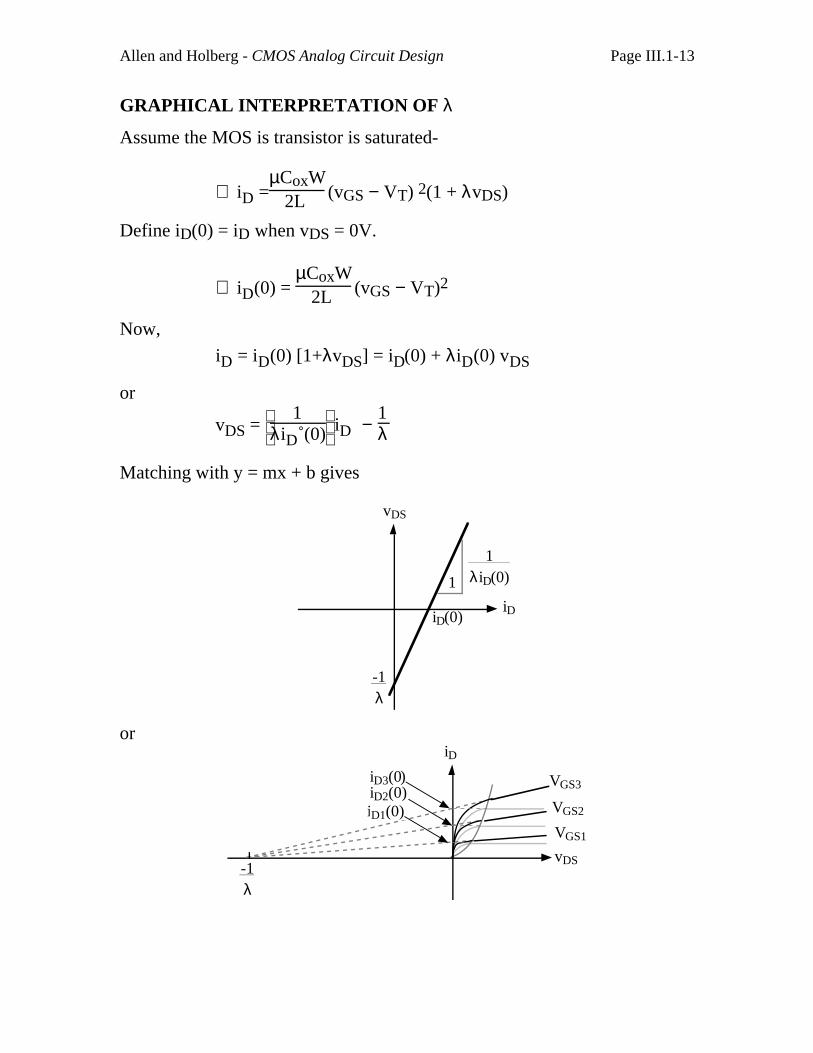
GRAPHICAL INTERPRETATION OF λ
Assume the MOS is transistor is saturated-
∴ iD =µCoxW
2L (vGS − VT) 2(1 + λvDS)
Define iD(0) = iD when vDS = 0V.
∴ iD(0) = µCoxW
2L (vGS − VT)2
Now,
iD = iD(0) [1+λvDS] = iD(0) + λiD(0) vDS
or
vDS =
1
λiD (0) iD − 1λ
Matching with y = mx + b gives
vDS
iDiD(0)
1λiD(0)1
-1λ
or
vDS
iD
-1λ
iD1(0)iD2(0)iD3(0 VGS3
VGS2
VGS1
)
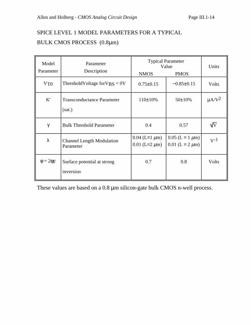
Allen and Holberg - CMOS Analog Circuit Design Page III.1-14
SPICE LEVEL 1 MODEL PARAMETERS FOR A TYPICAL
BULK CMOS PROCESS (0.8µm)
Model
Parameter
Parameter
Description
Typical Parameter Value
NMOS PMOS
Units
VT0 ThresholdVoltage forVBS = 0V 0.75±0.15 −0.85±0.15 Volts
K' Transconductance Parameter
(sat.)
110±10% 50±10% µA/V2
γ Bulk Threshold Parameter 0.4 0.57 V
λ Channel Length ModulationParameter
0.04 (L=1 µm)
0.01 (L=2 µm)
0.05 (L = 1 µm)
0.01 (L = 2 µm)V-1
φ = 2φF Surface potential at strong
inversion
0.7 0.8 Volts
These values are based on a 0.8 µm silicon-gate bulk CMOS n-well process.

Allen and Holberg - CMOS Analog Circuit Design Page III.1-15
WEAK INVERSION MODEL (Simple)
0 vGS
iD
VONVT 0 vGS
iD (nA)
VONVT
Weak inversion
region Strong inversion
region
1.0
10.0
100.0
1000.0
This model is appropriate for hand calculations but it does not accommodatea smooth transition into the strong-inversion region.
iD ≅ WL IDO exp
qvGS
nkT
The transition point where this relationship is valid occurs at approximately
vgs < VT + n kTq
Weak-Moderate-Strong Inversion Approximation
0 vGS
iD (nA)
Weak inversion
region Strong inversion
region
1.0
10.0
100.0
1000.0
Moderate inversion region
Allen and Holberg - CMOS Analog Circuit Design Page III.2-1
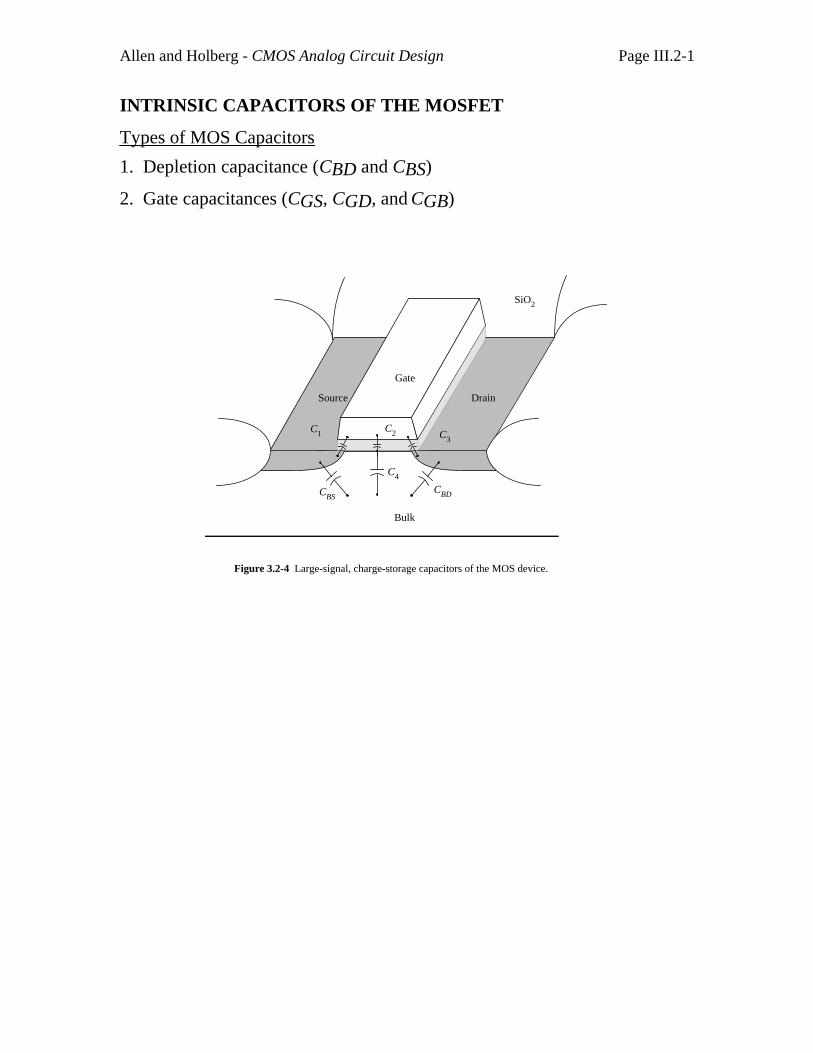
INTRINSIC CAPACITORS OF THE MOSFET
Types of MOS Capacitors
1. Depletion capacitance (CBD and CBS)
2. Gate capacitances (CGS, CGD, and CGB)
Figure 3.2-4 Large-signal, charge-storage capacitors of the MOS device.
SiO2
Bulk
Source Drain
Gate
CBSCBD
C4
C1 C2 C3
Allen and Holberg - CMOS Analog Circuit Design Page III.2-2
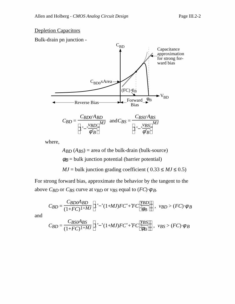
Depletion Capacitors
Bulk-drain pn junction -CBD
CBD0
VBDφBReverse Bias Forward
Bias
(FC).φB
Capacitanceapproximationfor strong for-ward bias
xArea
CBD = CBD0 ABD
1 − vBDφ B
MJ andCBS =
CBS0 ABS
1 − vBSφ B
MJ
where,
ABD (ABS) = area of the bulk-drain (bulk-source)
φΒ = bulk junction potential (barrier potential)
MJ = bulk junction grading coefficient ( 0.33 ≤ MJ ≤ 0.5)
For strong forward bias, approximate the behavior by the tangent to the
above CBD or CBS curve at vBD or vBS equal to (FC)·φ B.
CBD = CBD0ABD
(1+FC)1+MJ
1 − (1+MJ)FC + FC
vBD
φB , vBD > (FC)·φ B
and
CBD = CBS0ABS
(1+FC)1+MJ
1 − (1+MJ)FC + FC
vBS
φB , vBS > (FC)·φ B
Allen and Holberg - CMOS Analog Circuit Design Page III.2-3
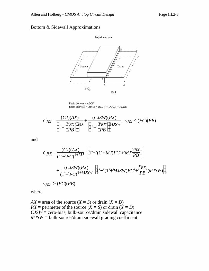
Bottom & Sidewall Approximations
SiO2
Polysilicon gate
Bulk
A B
CD
EF
GH
Drain bottom = ABCD Drain sidewall = ABFE + BCGF + DCGH + ADHE
Source Drain
CBX = (CJ)(AX)
1 −
vBX
PBMJ
+ (CJSW)(PX)
1 −
vBX
PBMJSW
, vBX ≤ (FC)(PB)
and
CBX = (CJ)(AX)
(1 − FC)1+MJ
1 − (1 + MJ)FC + MJ vBXPB
+ (CJSW)(PX)
(1 − FC)1+MJSW
1 − (1 + MJSW)FC + vBXPB (MJSW) ,
vBX ≥ (FC)(PB)
where
AX = area of the source (X = S) or drain (X = D)PX = perimeter of the source (X = S) or drain (X = D)CJSW = zero-bias, bulk-source/drain sidewall capacitanceMJSW = bulk-source/drain sidewall grading coefficient
Allen and Holberg - CMOS Analog Circuit Design Page III.2-4
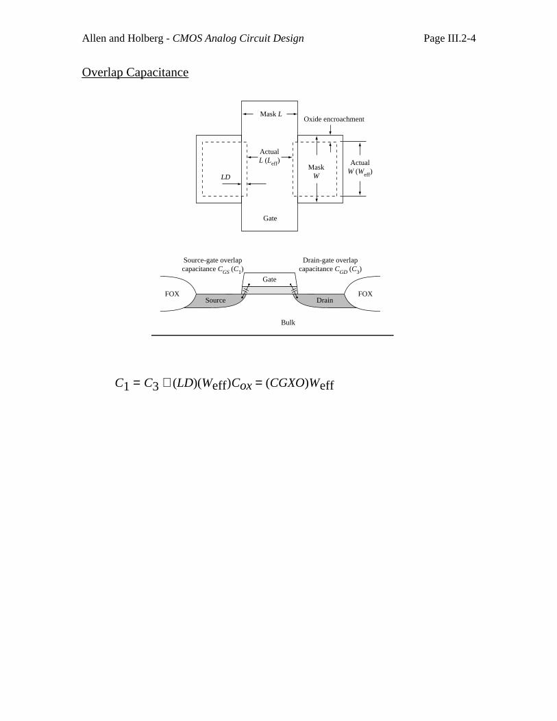
Overlap Capacitance
Figure 3.2-5 Overlap capacitances of an MOS transistor. (a) Top view showing the overlap between the source or drain and the gate. (b) Side view.
Bulk
LDMask
W
Oxide encroachment
ActualL (Leff)
Gate
Mask L
Source-gate overlap capacitance CGS (C1)
Drain-gate overlap capacitance CGD (C3)
Source Drain
Gate
FOX FOX
ActualW (Weff)
C1 = C3 ≅ (LD)(Weff)Cox = (CGXO)Weff
Allen and Holberg - CMOS Analog Circuit Design Page III.2-5
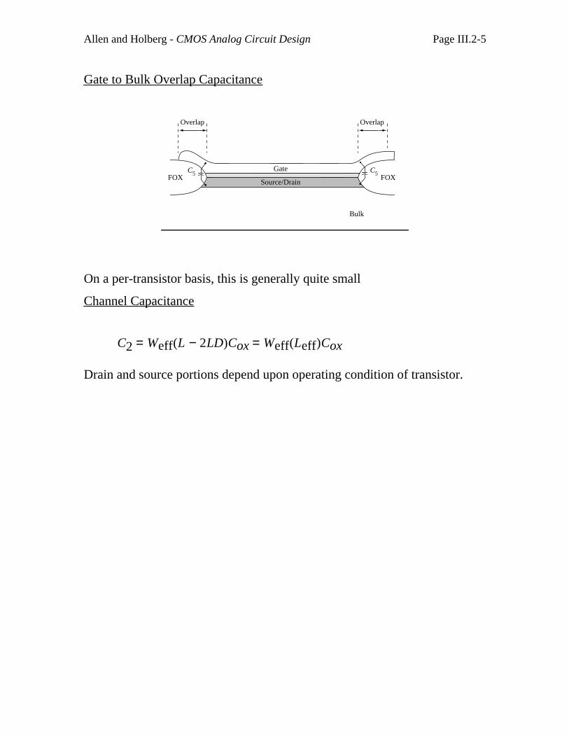
Gate to Bulk Overlap Capacitance
Figure 3.2-6 Gate-bulk overlap capacitances.
Bulk
Overlap Overlap
Source/Drain
GateFOX FOX
C5 C5
On a per-transistor basis, this is generally quite small
Channel Capacitance
C2 = Weff(L − 2LD)Cox = Weff(Leff)Cox
Drain and source portions depend upon operating condition of transistor.
Allen and Holberg - CMOS Analog Circuit Design Page III.2-6
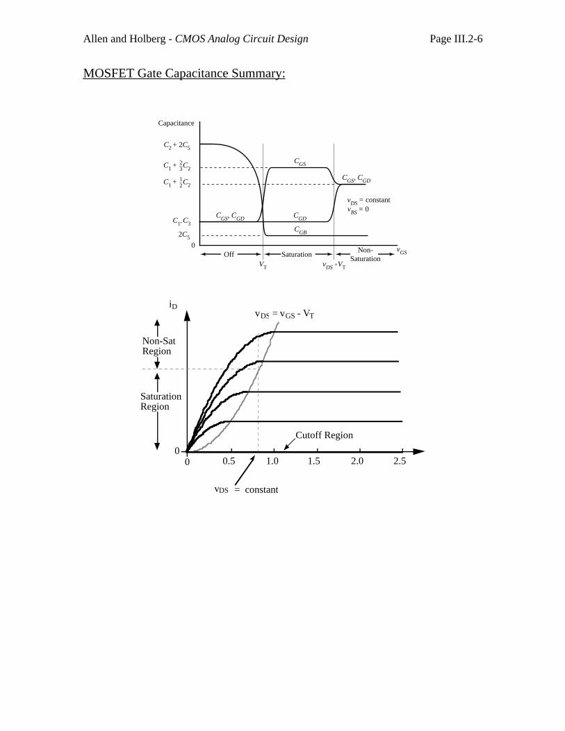
MOSFET Gate Capacitance Summary:
0 vGS
Figure 3.2-7 Voltage dependence of CGS, CGD, and CGB as a function of VGSwith VDS constang and VBS = 0.
CGS
CGS, CGD
CGD
CGB
CGS, CGD
C2 + 2C5
C1 +23_C2
C1 +12_C2
C1, C3
2C5
VT vDS +VT
Off SaturationNon-
Saturation
vDS = constant vBS = 0
Capacitance
vDS - VT
iD
00 0.5 1.0 1.5 2.0 2.5
Non-SatRegion
Saturation Region
Cutoff Region
= vGS
vDS = constant
Allen and Holberg - CMOS Analog Circuit Design Page III.2-7
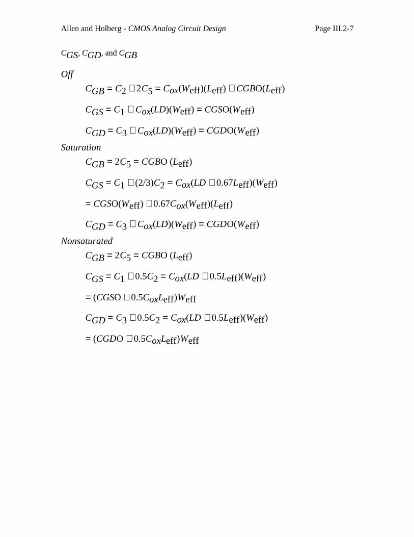
CGS, CGD, and CGB
Off
CGB = C2 + 2C5 = Cox(Weff)(Leff) + CGBO(Leff)
CGS = C1 ≅ Cox(LD)(Weff) = CGSO(Weff)
CGD = C3 ≅ Cox(LD)(Weff) = CGDO(Weff)
Saturation
CGB = 2C5 = CGBO (Leff)
CGS = C1 + (2/3)C2 = Cox(LD + 0.67Leff)(Weff)
= CGSO(Weff) + 0.67Cox(Weff)(Leff)
CGD = C3 ≅ Cox(LD)(Weff) = CGDO(Weff)
Nonsaturated
CGB = 2C5 = CGBO (Leff)
CGS = C1 + 0.5C2 = Cox(LD + 0.5Leff)(Weff)
= (CGSO + 0.5CoxLeff)Weff
CGD = C3 + 0.5C2 = Cox(LD + 0.5Leff)(Weff)
= (CGDO + 0.5CoxLeff)Weff
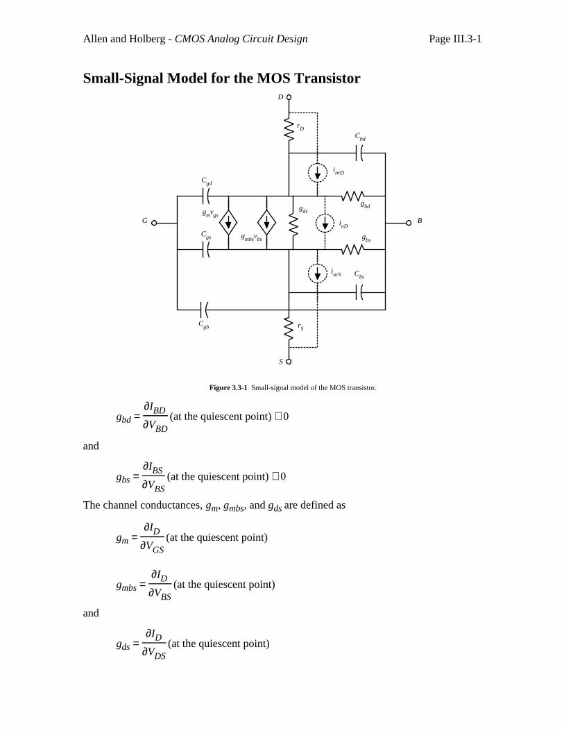
Allen and Holberg - CMOS Analog Circuit Design Page III.3-1
Small-Signal Model for the MOS Transistor
B
D
S
G inD
Cbd
Cgd
Cgs
Cgb
gmvgs
rD
rS
Cbs
Figure 3.3-1 Small-signal model of the MOS transistor.
gmbsvbs
gds
gbs
gbd
inrD
inrS
gbd = ∂IBD
∂VBD (at the quiescent point) ≅ 0
and
gbs = ∂IBS
∂VBS (at the quiescent point) ≅ 0
The channel conductances, gm, gmbs, and gds are defined as
gm = ∂ID
∂VGS (at the quiescent point)
gmbs = ∂ID
∂VBS (at the quiescent point)
and
gds = ∂ID
∂VDS (at the quiescent point)
Allen and Holberg - CMOS Analog Circuit Design Page III.3-2
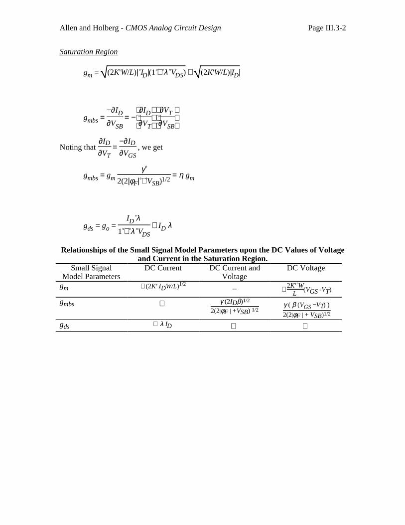
Saturation Region
gm = (2K'W/L)| ID|(1 + λ VDS) ≅ (2K'W/L)|ID|
gmbs = −∂ID
∂VSB = −
∂ID
∂VT
∂VT
∂VSB
Noting that ∂ID
∂VT =
−∂ID
∂VGS , we get
gmbs = gm γ
2(2|φF| + VSB)1/2 = η gm
gds = go = ID λ
1 + λ VDS ≅ ID λ
Relationships of the Small Signal Model Parameters upon the DC Values of Voltageand Current in the Saturation Region.
Small SignalModel Parameters
DC Current DC Current andVoltage
DC Voltage
gm ≅ (2K' IDW/L)1/2 _ ≅ 2K' WL
(VGS -VT)
gmbs γ (2IDβ)1/2
2(2|φF | +VSB) 1/2γ ( β (VGS −VT) )
2(2|φF | + VSB)1/2
gds ≅ λ ID
Allen and Holberg - CMOS Analog Circuit Design Page III.3-3
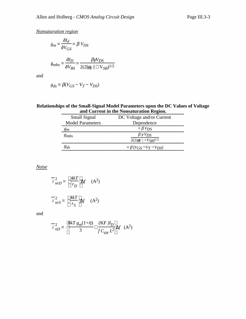
N onsaturation region
gm = ∂Id
∂VGS = β VDS
gmbs = ∂ID
∂VBS =
βγVDS
2(2|φF | + VSB)1/2
and
gds = β(VGS − VT − VDS)
Relationships of the Small-Signal Model Parameters upon the DC Values of Voltageand Current in the Nonsaturation Region.
Small SignalModel Parameters
DC Voltage and/or CurrentDependence
gm = β VDSgmbs β γ VDS
2(2|φF | +VSB)1/2
gds = β (VGS −VT −VDS)
Noise
i2nrD =
4kTrD
∆f (A2)
i2nrS =
4kTrS
∆f (A2)
and
i2nD =
8kT gm(1+η)
3 +
(KF )IDf Cox L2 ∆f (A2)
Allen and Holberg - CMOS Analog Circuit Design Page III.4-1
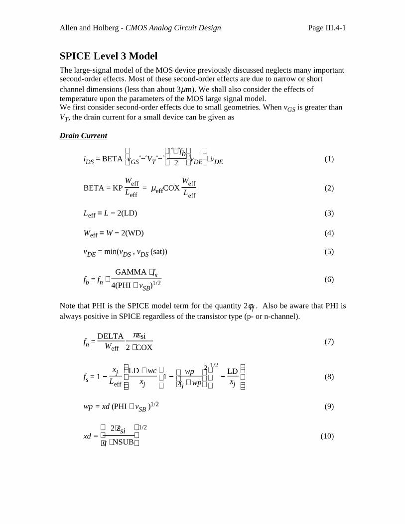
SPICE Level 3 ModelThe large-signal model of the MOS device previously discussed neglects many importantsecond-order effects. Most of these second-order effects are due to narrow or shortchannel dimensions (less than about 3µm). We shall also consider the effects oftemperature upon the parameters of the MOS large signal model.We first consider second-order effects due to small geometries. When vGS is greater thanVT, the drain current for a small device can be given as
Drain Current
iDS = BETA
vGS − VT −
1 + fb
2 vDE ⋅ vDE (1)
BETA = KP WeffLeff
= µeffCOX Weff Leff
(2)
Leff = L − 2(LD) (3)
Weff = W − 2(WD) (4)
vDE = min(vDS , vDS (sat)) (5)
fb = fn + GAMMA ⋅ fs
4(PHI + vSB)1/2 (6)
Note that PHI is the SPICE model term for the quantity 2φf . Also be aware that PHI isalways positive in SPICE regardless of the transistor type (p- or n-channel).
fn = DELTA
Weff
πεsi
2 ⋅ COX(7)
fs = 1 − xj
Leff
LD + wc
xj
1 −
wp
xj + wp
2 1/2
− LDxj
(8)
wp = xd (PHI + vSB )1/2 (9)
xd =
2⋅εsi
q ⋅ NSUB 1/2
(10)
Allen and Holberg - CMOS Analog Circuit Design Page III.4-2
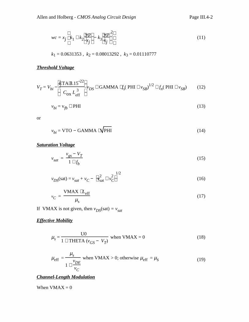
wc = xj
k1 + k2
wp
xj − k3
wp
xj
2(11)
k1 = 0.0631353 , k2 = 0.08013292 , k3 = 0.01110777
Threshold V oltage
VT = Vbi −
ETA⋅8.15-22
Cox L 3eff
vDS + GAMMA ⋅ fs( PHI + vSB)1/2 + fn( PHI + vSB) (12)
vbi = vfb + PHI (13)
or
vbi = VTO − GAMMA ⋅ PHI (14)
Saturation Voltage
vsat = vgs − VT
1 + fb(15)
vDS(sat) = vsat + vC − v2sat + v
2C
1/2 (16)
vC = VMAX ⋅ Leff
µs(17)
If VMAX is not given, then vDS(sat) = vsat
Effective Mobility
µs = U0
1 + THETA (vGS − VT) when VMAX = 0 (18)
µeff = µs
1 + vDEvC
when VMAX > 0; otherwise µeff = µs (19)
Channel-Length Modulation
When VMAX = 0
Allen and Holberg - CMOS Analog Circuit Design Page III.4-3
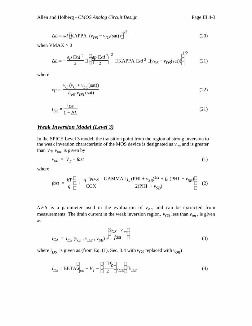
∆L = xd KAPPA (vDS − vDS(sat))1/2
(20)
when VMAX > 0
∆L = − ep ⋅ xd 2
2 +
ep ⋅ xd 2
2 2
+ KAPPA ⋅ xd 2 ⋅ (vDS − vDS(sat))
1/2
(21)
where
ep = vC (vC + vDS(sat))
Leff vDS (sat)(22)
iDS = iDS
1 − ∆L(21)
Weak Inversion Model (Level 3)
In the SPICE Level 3 model, the transition point from the region of strong inversion tothe weak inversion characteristic of the MOS device is designated as von and is greaterthan VT. von is given by
von = VT + fast (1)
where
fast = kTq
1 + q ⋅ NFSCOX
+ GAMMA ⋅ fs (PHI + vSB)1/2 + fn (PHI + vSB)
2(PHI + vSB) (2)
N F S is a parameter used in the evaluation of von and can be extracted frommeasurements. The drain current in the weak inversion region, vGS less than von , is givenas
iDS = iDS (von , vDE , vSB) e
vGS - von
fast (3)
where iDS is given as (from Eq. (1), Sec. 3.4 with vGS replaced with von)
iDS = BETA
von − VT −
1 + fb
2 vDE ⋅ vDE (4)
Allen and Holberg - CMOS Analog Circuit Design Page III.4-4
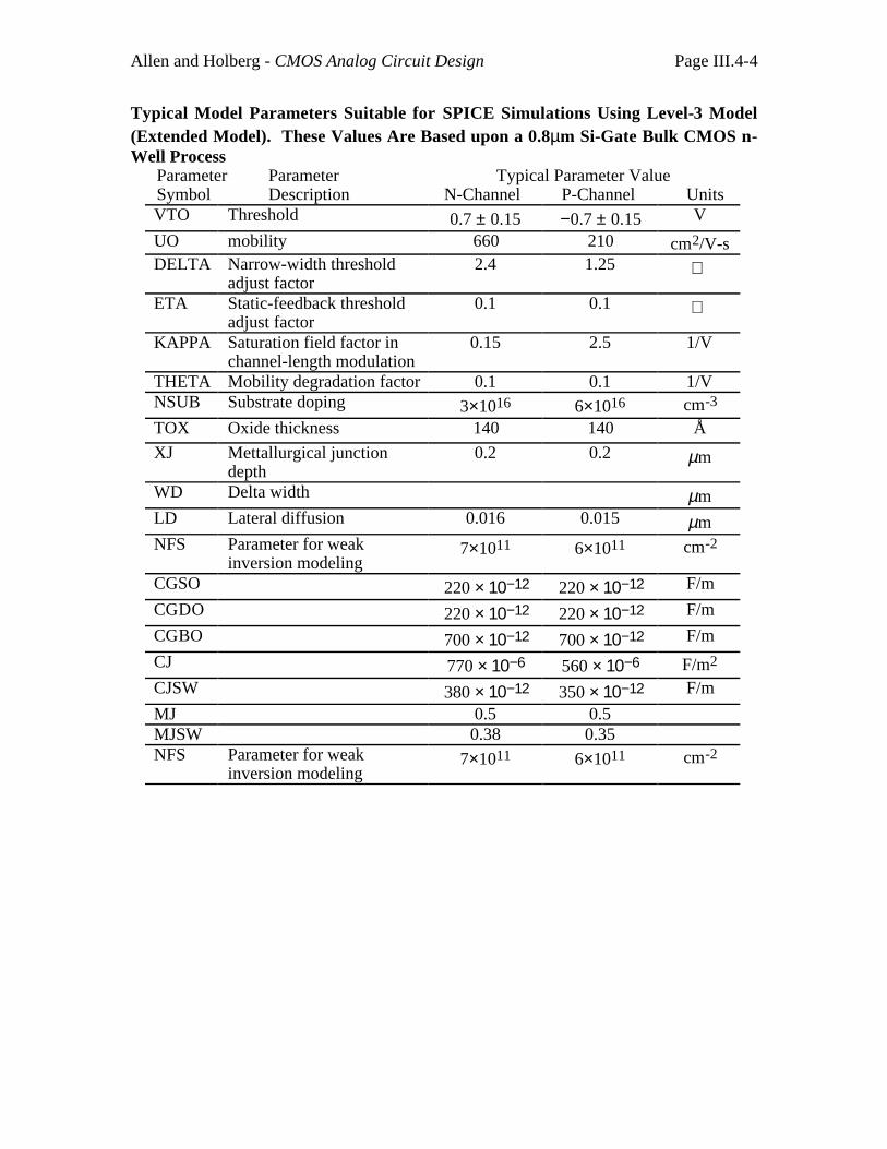
Typical Model Parameters Suitable for SPICE Simulations Using Level-3 Model(Extended Model). These Values Are Based upon a 0.8µm Si-Gate Bulk CMOS n-Well Process
Parameter Parameter Typical Parameter ValueSymbol Description N-Channel P-Channel UnitsVTO Threshold 0.7 ± 0.15 −0.7 ± 0.15 V
UO mobility 660 210 cm2/V-sDELTA Narrow-width threshold
adjust factor2.4 1.25
ETA Static-feedback thresholdadjust factor
0.1 0.1
KAPPA Saturation field factor inchannel-length modulation
0.15 2.5 1/V
THETA Mobility degradation factor 0.1 0.1 1/VNSUB Substrate doping 3×10¹⁶ 6×1016 cm-3
TOX Oxide thickness 140 140 Å
XJ Mettallurgical junctiondepth
0.2 0.2 µm
WD Delta width µmLD Lateral diffusion 0.016 0.015 µmNFS Parameter for weak
inversion modeling7×1011 6×1011 cm-2
CGSO 220 × 10−12 220 × 10−12 F/m
CGDO 220 × 10−12 220 × 10−12 F/m
CGBO 700 × 10−12 700 × 10−12 F/m
CJ 770 × 10−6 560 × 10−6 F/m2
CJSW 380 × 10−12 350 × 10−12 F/m
MJ 0.5 0.5MJSW 0.38 0.35NFS Parameter for weak
inversion modeling7×1011 6×1011 cm-2
Allen and Holberg - CMOS Analog Circuit Design Page III.4-5
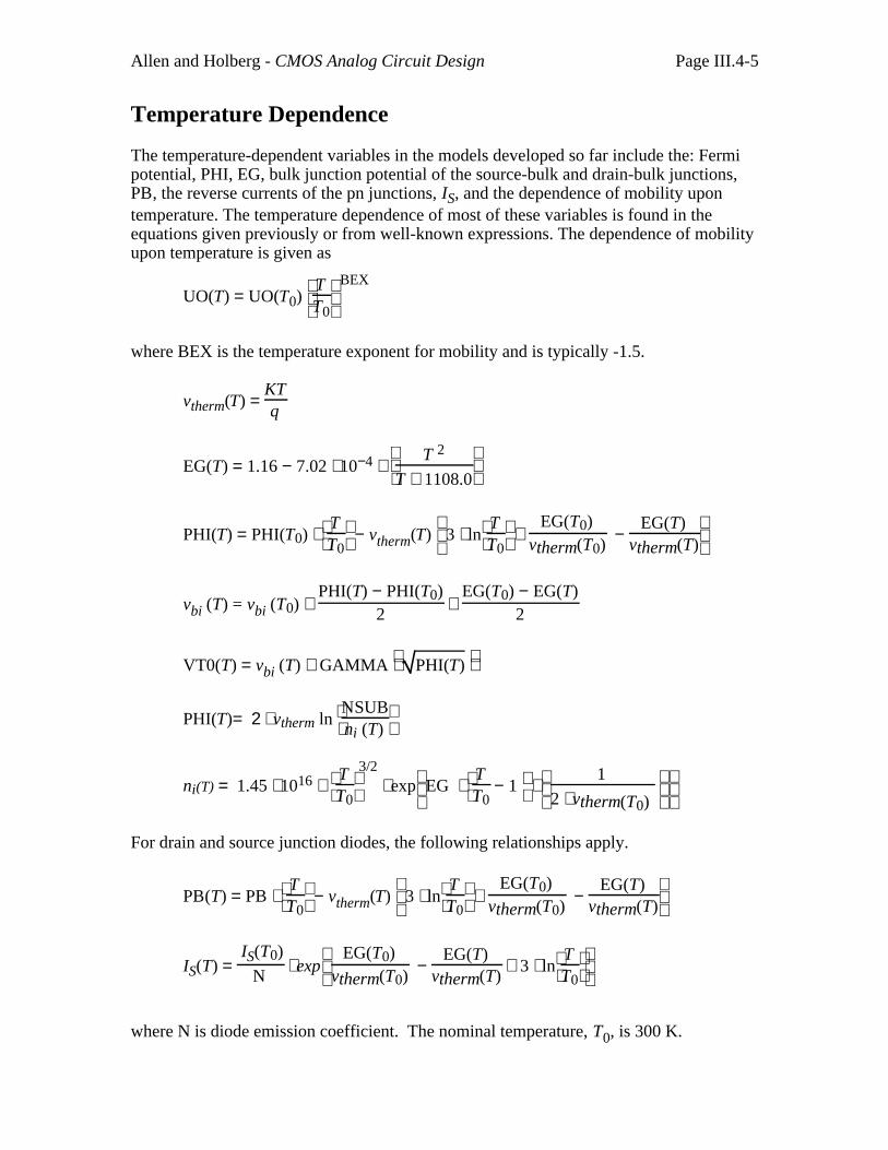
Temperature Dependence
The temperature-dependent variables in the models developed so far include the: Fermipotential, PHI, EG, bulk junction potential of the source-bulk and drain-bulk junctions,PB, the reverse currents of the pn junctions, IS, and the dependence of mobility upontemperature. The temperature dependence of most of these variables is found in theequations given previously or from well-known expressions. The dependence of mobilityupon temperature is given as
UO(T) = UO(T0)
T
T0 BEX
where BEX is the temperature exponent for mobility and is typically -1.5.
vtherm(T) = KTq
EG(T) = 1.16 − 7.02 ⋅ 10−4 ⋅
T 2
T + 1108.0
PHI(T) = PHI(T0) ⋅
T
T0 − vtherm(T)
3 ⋅ ln
T
T0 +
EG(T0)vtherm(T0)
− EG(T)
vtherm(T)
vbi (T) = vbi (T0) + PHI(T) − PHI(T0)
2 +
EG(T0) − EG(T)2
VT0(T) = vbi (T) + GAMMA
PHI(T)
PHI(T)= 2 ⋅ vtherm ln
NSUB
ni (T)
ni(T) = 1.45 ⋅ 1016 ⋅
T
T0
3/2 ⋅ exp
EG ⋅
T
T0 − 1 ⋅
1
2 ⋅ vtherm(T0)
For drain and source junction diodes, the following relationships apply.
PB(T) = PB ⋅
T
T0 − vtherm(T)
3 ⋅ ln
T
T0 +
EG(T0)vtherm(T0)
− EG(T)
vtherm(T)
IS(T) = IS(T0)
N ⋅ exp
EG(T0)
vtherm(T0) −
EG(T)vtherm(T)
+ 3 ⋅ ln
T
T0
where N is diode emission coefficient. The nominal temperature, T0, is 300 K.
Allen and Holberg - CMOS Analog Circuit Design Page III.3-1
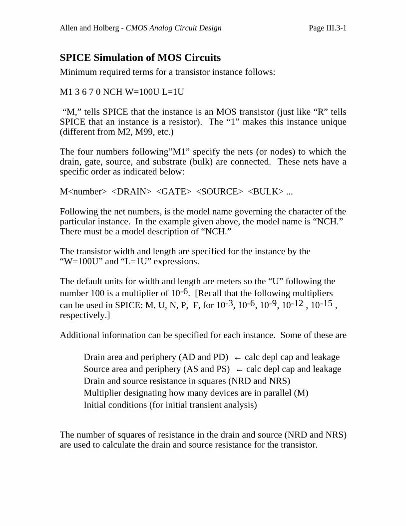
SPICE Simulation of MOS CircuitsMinimum required terms for a transistor instance follows:
M1 3 6 7 0 NCH W=100U L=1U
“M,” tells SPICE that the instance is an MOS transistor (just like “R” tellsSPICE that an instance is a resistor). The “1” makes this instance unique(different from M2, M99, etc.)
The four numbers following”M1” specify the nets (or nodes) to which thedrain, gate, source, and substrate (bulk) are connected. These nets have aspecific order as indicated below:
M<number> <DRAIN> <GATE> <SOURCE> <BULK> ...
Following the net numbers, is the model name governing the character of theparticular instance. In the example given above, the model name is “NCH.”There must be a model description of “NCH.”
The transistor width and length are specified for the instance by the“W=100U” and “L=1U” expressions.
The default units for width and length are meters so the “U” following thenumber 100 is a multiplier of 10-6. [Recall that the following multiplierscan be used in SPICE: M, U, N, P, F, for 10-3, 10-6, 10-9, 10-12 , 10-15 ,respectively.]
Additional information can be specified for each instance. Some of these are
Drain area and periphery (AD and PD) ← calc depl cap and leakageSource area and periphery (AS and PS) ← calc depl cap and leakageDrain and source resistance in squares (NRD and NRS)Multiplier designating how many devices are in parallel (M)Initial conditions (for initial transient analysis)
The number of squares of resistance in the drain and source (NRD and NRS)are used to calculate the drain and source resistance for the transistor.

Allen and Holberg - CMOS Analog Circuit Design Page III.3-2
Geometric Multiplier: M
To apply the “unit-matching” principle, use the geometric multiplier featurerather than scale W/L.
This:
M1 3 2 1 0 NCH W=20U L=1U
is not the same as this:
M1 3 2 1 0 NCH W=10U L=1U M=2
The following dual instantiation is equivalent to using a multiplier
M1A 3 2 1 0 NCH W=10U L=1UM1B 3 2 1 0 NCH W=10U L=1U
(a)M1 3 2 1 0 NCH W=20U L=1U. (b) M1 3 2 1 0 NCH W=10U L=1U M=1. .
(a) (b)
Allen and Holberg - CMOS Analog Circuit Design Page III.3-3
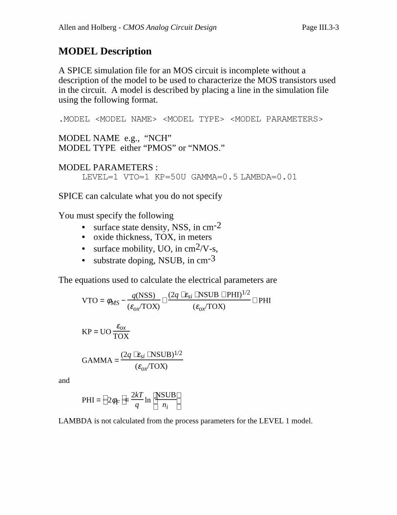
MODEL Description
A SPICE simulation file for an MOS circuit is incomplete without adescription of the model to be used to characterize the MOS transistors usedin the circuit. A model is described by placing a line in the simulation fileusing the following format.
.MODEL <MODEL NAME> <MODEL TYPE> <MODEL PARAMETERS>
MODEL NAME e.g., “NCH”MODEL TYPE either “PMOS” or “NMOS.”
MODEL PARAMETERS :LEVEL=1 VTO=1 KP=50U GAMMA=0.5 LAMBDA=0.01
SPICE can calculate what you do not specify
You must specify the following• surface state density, NSS, in cm-2• oxide thickness, TOX, in meters• surface mobility, UO, in cm2/V-s,• substrate doping, NSUB, in cm-3
The equations used to calculate the electrical parameters are
VTO = φMS − q(NSS)
(εox/TOX) +
(2q ⋅ εsi ⋅ NSUB ⋅ PHI)1/2
(εox/TOX) + PHI
KP = UO εox
TOX
GAMMA = (2q ⋅ εsi ⋅ NSUB)1/2
(εox/TOX)
and
PHI = 2φF =
2kTq
ln
NSUB
ni
LAMBDA is not calculated from the process parameters for the LEVEL 1 model.
Allen and Holberg - CMOS Analog Circuit Design Page III.3-4
Other parameters:
IS: Reverse current of the drain-bulk or source-bulk junctions in AmpsJS: Reverse-current density in A/m2
JS requires the specification of AS and AD on the model line. If IS isspecified, it overrides JS. The default value of IS is usually 10-14 A.
RD: Drain ohmic resistance in ohmsRS: Source ohmic resistance in ohms
RSH: Sheet resistance in ohms/square. RSH is overridden if RD orRS are entered. To use RSH, the values of NRD and NRS must beentered on the model line.
The drain-bulk and source-bulk depletion capacitorsCJ: Bulk bottom plate junction capacitanceMJ: Bottom plate junction grading coefficientCJSW: Bulk sidewall junction capacitanceMJSW: Sidewall junction grading coefficient
If CJ is entered as a model parameter it overrides the calculation of CJ using NSUB,otherwise, CJ is calculated using NSUB.
If CBD and CBS are entered, these values override CJ and NSUB calculations.
In order for CJ to result in an actual circuit capacitance, the transistor instance mustinclude AD and AS.
In order for CJSW to result in an actual circuit capacitance, the transistor instance mustinclude PD and PS.
CGSO: Gate-Source overlap capacitance (at zero bias)CGDO: Gate-Drain overlap capacitance (at zero bias)
AF: Flicker noise exponentKF: Flicker noise coefficient
TPG: Indicates type of gate material relative to the substrateTPG=1 > gate material is opposite of the substrateTPG=-1 > gate material is the same as the substrateTPG=0 > gate material is aluminum
XQC: Channel charge flag and fraction of channel charge attributed to the drain
Allen and Holberg - CMOS Analog Circuit Design Page IV.0-1
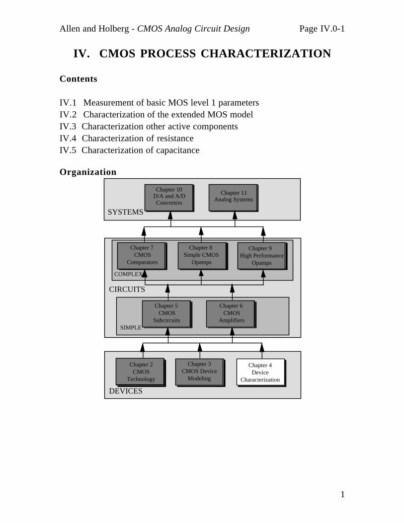
1
IV. CMOS PROCESS CHARACTERIZATION
Contents
IV.1 Measurement of basic MOS level 1 parametersIV.2 Characterization of the extended MOS modelIV.3 Characterization other active componentsIV.4 Characterization of resistanceIV.5 Characterization of capacitance
Organization
DEVICES
SYSTEMS
CIRCUITS
Chapter 2CMOS
Technology
Chapter 3CMOS Device
Modeling
Chapter 4Device
Characterization
Chapter 7 CMOS
Comparators
Chapter 8 Simple CMOS
Opamps
Chapter 9 High Performance
Opamps
Chapter 5 CMOS
Subcircuits
Chapter 6 CMOS
Amplifiers
Chapter 10D/A and A/D Converters
Chapter 11Analog Systems
SIMPLE
COMPLEX
Allen and Holberg - CMOS Analog Circuit Design Page IV.1-1
1
I. Characterization of the Simple Transistor Model
Determine VT0(VSB = 0), K', γ, and λ .Terminology:
K'S for the saturation regionK'L for the nonsaturation region
iD = K'S
Weff
2Leff (vGS - VT)2 (1 + λ vDS ) (1)
iD = K'L
Weff
Leff
(vG S - V T ) vD S - v
2DS2 (2)
VT = VT0 + γ 2 |φF | + vS B - 2|φF| (3)
Assume that vDS is chosen such that the λ vDS << 1vSB =0 -> VT = VT0.
Therefore, Eq. (1) simplifies to
iD = K’S
Weff
2Leff (vGS - VT0)2 (4)
This equation can be manipulated algebraically to obtain the following
i1/2D =
K'S Weff
2Leff
1/2
vGS -
K'S Weff
2Leff
1/2
VT0 (5)
which has the form
y = mx + b (6)
y = i1/2D (7)
x = vGS (8)
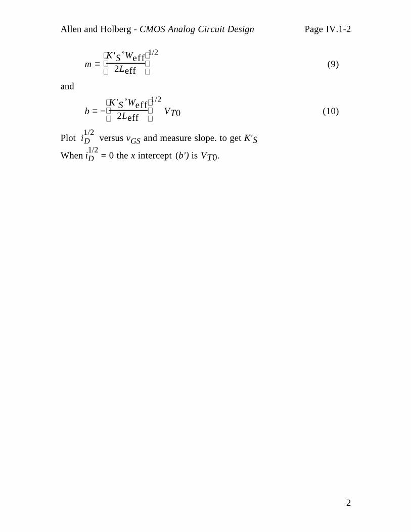
Allen and Holberg - CMOS Analog Circuit Design Page IV.1-2
2
m =
K'S Weff
2Leff
1/2
(9)
and
b = −
K'S Weff
2Leff
1/2
VT0 (10)
Plot i1/2D versus vGS and measure slope. to get K'S
When i1/2D = 0 the x intercept (b') is VT0.
Allen and Holberg - CMOS Analog Circuit Design Page IV.1-3
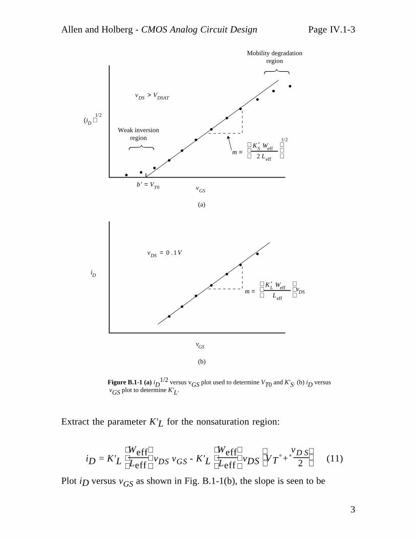
3
Figure B.1-1 (a) iD1/2 versus vGS plot used to determine VT0 and K'S. (b) iD versus
vGS plot to determine K'L.
iD
iD( )1/2
vDS > VDSAT
vDS = 0 .1V
m =′ K S Weff
2 Leff
1/2
vGS
vGS
′ b = VT0
Weak inversion region
Mobility degradation region
vDSm =′ K L Weff
Leff
(a)
(b)
Extract the parameter K'L for the nonsaturation region:
iD = K'L
Weff
Leff vDS vGS - K'L
Weff
Leff vDS
V T + vD S
2 (11)
Plot iD versus vGS as shown in Fig. B.1-1(b), the slope is seen to be
Allen and Holberg - CMOS Analog Circuit Design Page IV.1-4
4
m = ∆iD
∆vGS = K'L
Weff
Leff vDS (12)
Knowing the slope, the term K'L is easily determined to be
K'L = m
Leff
Weff
1
vDS (13)
Weff, Leff, and vDS must be known.
The approximate value µo can be extracted from the value of K'L
At this point, γ is unknown.
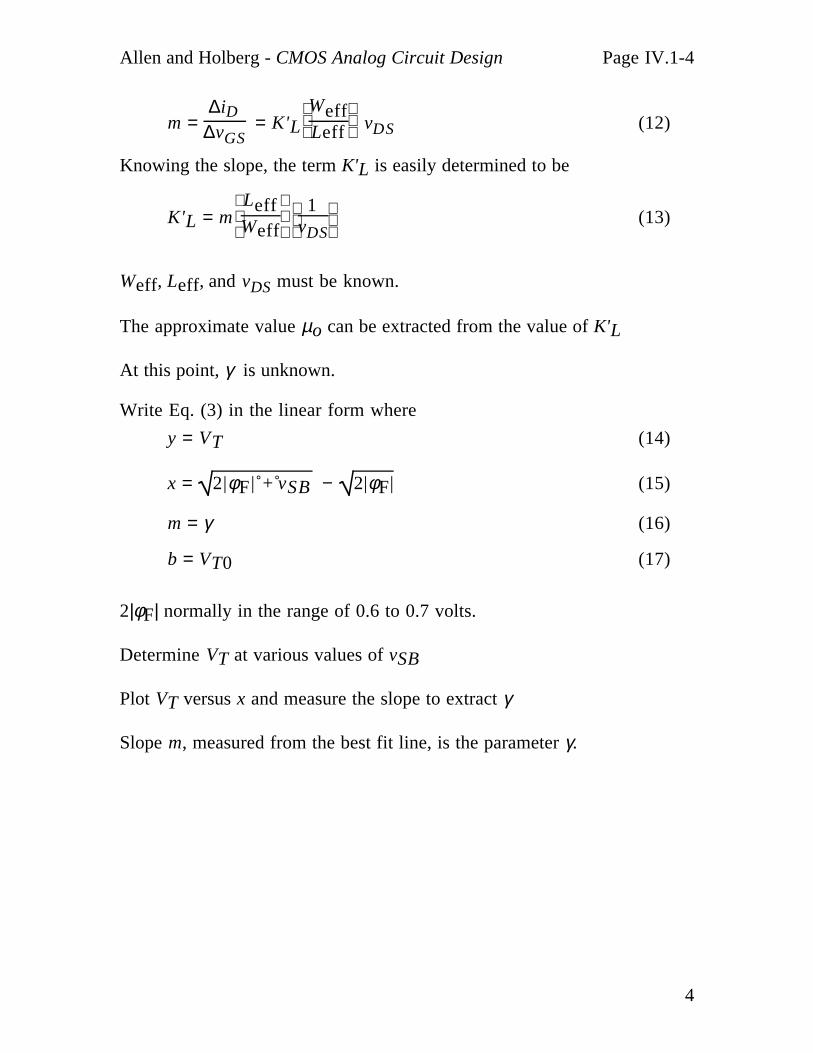
Write Eq. (3) in the linear form where
y = VT (14)
x = 2|φF| + vSB − 2|φF| (15)
m = γ (16)
b = VT0 (17)
2|φF| normally in the range of 0.6 to 0.7 volts.
Determine VT at various values of vSB
Plot VT versus x and measure the slope to extract γ
Slope m, measured from the best fit line, is the parameter γ.
Allen and Holberg - CMOS Analog Circuit Design Page IV.1-5
5
Figure B.1-2 iD1/2 versus vGS plot at different vSB values to determine γ.
VT
iD( )1/2
VSB = 1Vm = γ
vGS
VT0 VT1 VT2 VT3
VSB = 2 V
VSB = 3 V
VSB = 0V
Figure B.1-3 Plot of VT versus f(vSB) to determine γ.
vSB + 2 φF( )0.5
− 2 φF( )0.5
We still need to find λ, ∆L, and ∆W.λ should be determined for all device lengths that might be used.
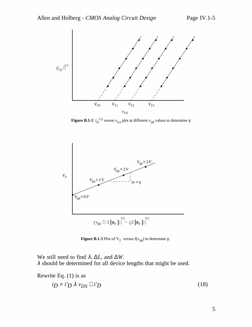
Rewrite Eq. (1) is as
iD = i'D λ vDS + i'D (18)
Allen and Holberg - CMOS Analog Circuit Design Page IV.1-6
6
which is in the familiar linear form where
y = iD (Eq. (1)) (19)
x = vDS (20)
m = λ i'D (21)
b = i'D (Eq. (4) with λ = 0) (22)
Plot iD versus vDS, and measure the slope of the data in the saturationregion, and divide that value by the y-intercept to getλ.
Figure B.1-4 Plot of iD versus vDS to determine λ.
i'Dm = λ
vDS
iD
i'D
Nonsaturation region
Saturation region
Calculating ∆L and ∆W.
Consider two transistors, with the same widths but different lengths,operating in the nonsaturation region with the same vDS. The widths of thetransistors are assumed to be very large so that W ≅ Weff. The large-signalmodel is given as
iD = K'LWeff
Leff
(vGS - VT0)vDS -
v
2DS2 (23)
Allen and Holberg - CMOS Analog Circuit Design Page IV.1-7
7
and
∂ID∂VGS
= gm =
K'L Weff
Leff VDS (24)
The aspect ratios (W/L) for the two transistors are
W1L1 + ∆ L (25)
and
W2L 2 + ∆ L (26)
Implicit in Eqs. (25) and (26) is that ∆L is assumed to be the same for bothtransistors. Combining Eq. (24) with Eqs. (25) and (26) gives
gm1 = K'LW
L 1 + ∆ L vDS (27)
and
gm2 = K'LW
L 2 + ∆ L vDS (28)
where W1 = W2 = W (and are assumed to equal the effective width). Withfurther algebraic manipulation of Eqs. (27) and (28), one can show that,
gm1gm1 - gm2
= L2 + ∆L
L 2 - L 1 (29)
which further yields
L2 + ∆L = Leff = (L2 - L1) gm1
gm1 - gm2 (30)
L2 and L1 known gm1 and gm2 can be measuredSimilarly for Weff :
W2 + ∆W = Weff = (W1 - W2)gm2
gm1 - gm2 (31)
Equation (31) is valid when two transistors have the same length butdifferent widths.
Allen and Holberg - CMOS Analog Circuit Design Page IV.1-8
8
One must be careful in determining ∆L (or ∆W) to make the lengths (orwidths) sufficiently different in order to avoid the numerical error due tosubtracting large numbers, and small enough that the transistor modelchosen is still valid for both transistors.
Allen and Holberg - CMOS Analog Circuit Design Page IV.3-1
1
II. Transistor Characterization for the Extended Model
Equations (1) and (2) represent a simplified version of the extended modelfor a relatively wide MOS transistor operating in the nonsaturation, strong-inversion region with VSB = 0.
iD = µsCoxW
L (vG S - V T )vD S -
v
2DS2 + γvDS 2|φF|
−
2γ
3 [(vDS + 2|φF|)1.5 - (2|φF|)]1.5 (1)
where W and L are effective electrical equivalents (dropping the subscript,“eff”, for convenience).
µs = µo
(UCRIT)εsi
Cox[vGS - VT - (UTRA)vDS]UEXP
(2)
Eq. (2) holds when the denominator term in the brackets is less than unity.Otherwise, µo = µs. To develop a procedure for extracting µo, considerthe case where mobility degradation effects are not being experienced, i.e.,µs = µo, Eq. (1) can be rewritten in general as
iD = µof(Cox, W, L, vGS, VT, vDS, γ, 2|φF|) (3)
This equation is a linear function of vGS and is in the familiar form of
y = mx + b (4)
where b = 0.
Plot iD versus the function, f(Cox, W , L , vGS, VT , vDS, γ, 2|φF|) andmeasure the slope = µo.
• The data are limited to the nonsaturation region (small vDS).• The transistor must be in the strong-inversion region (vGS > VT).• The transistor must operate below the critical-mobility point.
Keep vGS as low as possible without encroaching on the weak-inversionregion of operation.
Allen and Holberg - CMOS Analog Circuit Design Page IV.3-2
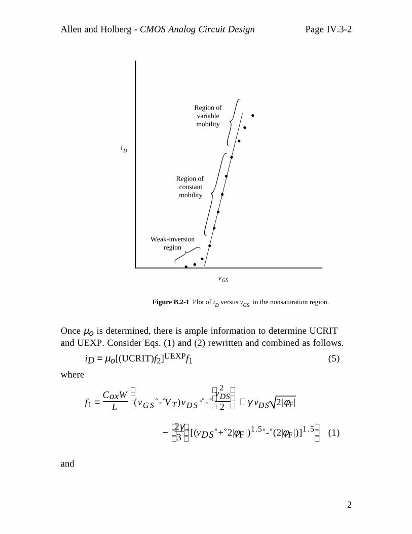
2
Figure B.2-1 Plot of iD versus vGS in the nonsaturation region.
vGS
iD
Region of variable mobility
Region of constant mobility
Weak-inversion region
Once µo is determined, there is ample information to determine UCRITand UEXP. Consider Eqs. (1) and (2) rewritten and combined as follows.
iD = µo[(UCRIT)f2]UEXPf1 (5)
where
f1 = CoxW
L (vG S - V T )vD S -
v
2DS2 + γ vDS 2|φF|
−
2γ
3 [(vDS + 2|φF|)1.5 - (2|φF|)]1.5 (1)
and
Allen and Holberg - CMOS Analog Circuit Design Page IV.3-3
3
f2 = ε s i
[vGS - VT - (UTRA)vDS]Cox (7)
The units of f1 and f2 are FV2/cm2 and cm/V respectively. Notice that f2includes the parameter UTRA, which is an unknown. UTRA is disabled inmost SPICE models.
Equation (5) can be manipulated algebraically to yield
log
iDf1
= log(µo) + UEXP[log(UCRIT)] + UEXP[log(f2)] (8)
This is in the familiar form of Eq. (4) with
x = log(f2) (9)
y = log
iDf1
(10)
m = UEXP (11)
b = log(µo) + UEXP[log(UCRIT)] (12)
By plotting Eq. (8) and measuring the slope, UEXP can be determined.The y-intercept can be extracted from the plot and UCRIT can bedetermined by back calculation given UEXP, µo, and the intercept, b.
Allen and Holberg - CMOS Analog Circuit Design Page IV.4-1
1
III. Characterization of Substrate Bipolar
Parameters of interest are: β dc, and JS.
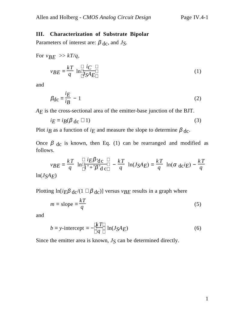
For vBE >> kT/q,
vBE = kTq ln
iC
JSAE (1)
and
βdc = iEiB
− 1 (2)
AE is the cross-sectional area of the emitter-base junction of the BJT.
iE = iB(β dc + 1) (3)
Plot iB as a function of iE and measure the slope to determine β dc.
Once β dc is known, then Eq. (1) can be rearranged and modified asfollows.
vBE = k Tq ln
iEβ dc
1 + β d c −
k Tq ln(JSAE) =
k Tq ln(α dciE) −
k Tq
ln(JSAE)
Plotting ln[iEβ dc/(1 + β dc)] versus vBE results in a graph where
m = slope = kTq (5)
and
b = y-intercept = −
k T
q ln(JSAE) (6)
Since the emitter area is known, JS can be determined directly.
Allen and Holberg - CMOS Analog Circuit Design Page IV.5-1
1
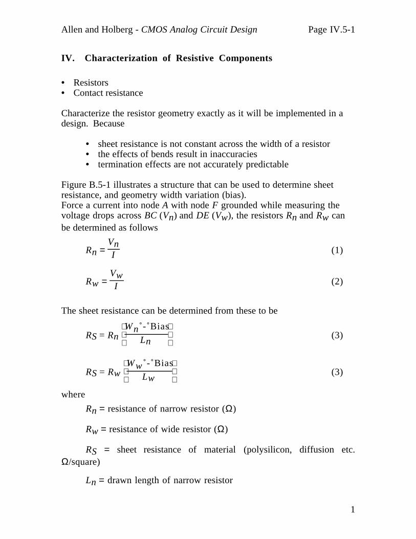
IV. Characterization of Resistive Components
• Resistors• Contact resistance
Characterize the resistor geometry exactly as it will be implemented in adesign. Because
• sheet resistance is not constant across the width of a resistor• the effects of bends result in inaccuracies• termination effects are not accurately predictable
Figure B.5-1 illustrates a structure that can be used to determine sheetresistance, and geometry width variation (bias).Force a current into node A with node F grounded while measuring thevoltage drops across BC (Vn) and DE (Vw), the resistors Rn and Rw canbe determined as follows
Rn = VnI (1)
Rw = VwI (2)
The sheet resistance can be determined from these to be
RS = Rn
Wn - Bias
Ln (3)
RS = Rw
Ww - Bias
Lw (3)
where
Rn = resistance of narrow resistor (Ω)
Rw = resistance of wide resistor (Ω)
RS = sheet resistance of material (polysilicon, diffusion etc.Ω/square)
Ln = drawn length of narrow resistor
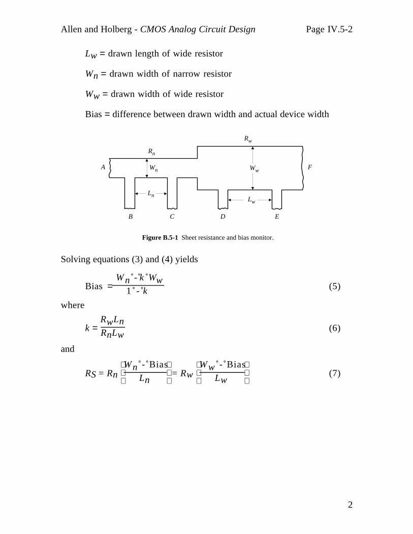
Allen and Holberg - CMOS Analog Circuit Design Page IV.5-2
2
Lw = drawn length of wide resistor
Wn = drawn width of narrow resistor
Ww = drawn width of wide resistor
Bias = difference between drawn width and actual device width
WwWn
LnLw
Rw
Rn
A F
B C D E
Figure B.5-1 Sheet resistance and bias monitor.
Solving equations (3) and (4) yields
Bias = W n - k Ww
1 - k (5)
where
k = RwLnRnLw
(6)
and
RS = Rn
Wn - Bias
Ln = Rw
Ww - Bias
Lw (7)
Allen and Holberg - CMOS Analog Circuit Design Page IV.5-3
3
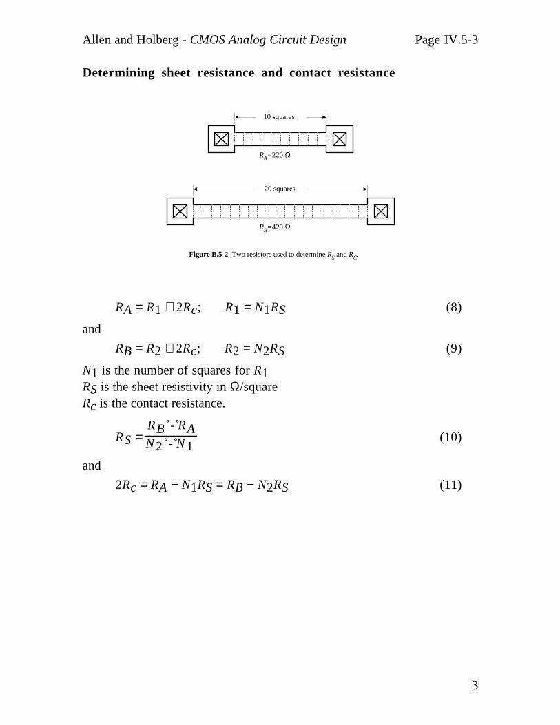
Determining sheet resistance and contact resistance
Figure B.5-2 Two resistors used to determine RS and RC.
10 squares
20 squares
RA=220 Ω
RB=420 Ω
RA = R1 + 2Rc; R1 = N1RS (8)
and
RB = R2 + 2Rc; R2 = N2RS (9)
N1 is the number of squares for R1RS is the sheet resistivity in Ω/squareRc is the contact resistance.
RS = RB - RAN 2 - N 1
(10)
and
2Rc = RA − N1RS = RB − N2RS (11)
Allen and Holberg - CMOS Analog Circuit Design Page IV.5-4
4
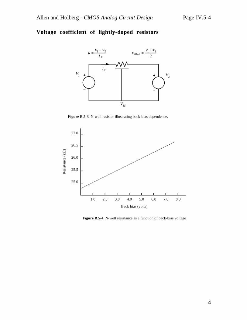
Voltage coefficient of lightly-doped resistors
Figure B.5-3 N-well resistor illustrating back-bias dependence.
V1 V2
R =V1 − V2
I RVBIAS =
V1 + V2
2
IR
VSS
Figure B.5-4 N-well resistance as a function of back-bias voltage
Back bias (volts)
1.0 2.0 3.0 4.0 5.0 6.0 7.0 8.0
Res
ista
nce
(kΩ
)
25.0
25.5
26.0
26.5
27.0

Allen and Holberg - CMOS Analog Circuit Design Page IV.5-5
5
Contact Resistance
Metal pads Diffusion or polysilicon
Metal pads
Pad 1
Pad 2
Pad 3 Pad 4
Pad 1
Pad 2
Pad 3
Pad 4
RC
R
RM
RM
RC
R
RC
Allen and Holberg - CMOS Analog Circuit Design Page IV.5-1
1
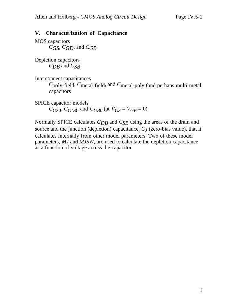
V. Characterization of Capacitance
MOS capacitorsCGS, CGD, and CGB
Depletion capacitorsCDB and CSB
Interconnect capacitancesCpoly-field, Cmetal-field, and Cmetal-poly (and perhaps multi-metalcapacitors
SPICE capacitor modelsCGS0, CGD0, and CGB0 (at VGS = VGB = 0).
Normally SPICE calculates CDB and CSB using the areas of the drain andsource and the junction (depletion) capacitance, CJ (zero-bias value), that itcalculates internally from other model parameters. Two of these modelparameters, MJ and MJSW, are used to calculate the depletion capacitanceas a function of voltage across the capacitor.
Allen and Holberg - CMOS Analog Circuit Design Page IV.5-2
2
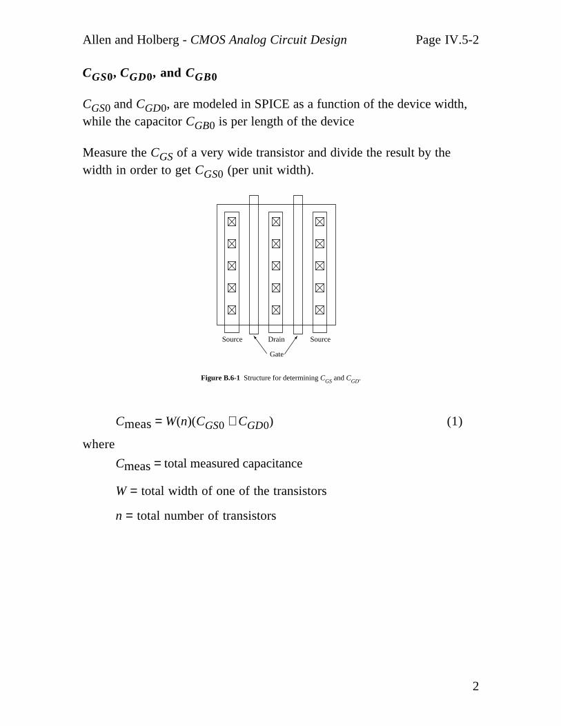
CGS0, CGD0, and CGB0
CGS0 and CGD0, are modeled in SPICE as a function of the device width,while the capacitor CGB0 is per length of the device
Measure the CGS of a very wide transistor and divide the result by thewidth in order to get CGS0 (per unit width).
Figure B.6-1 Structure for determining CGS and CGD.
Source
Gate
Drain Source
Cmeas = W(n)(CGS0 + CGD0) (1)
where
Cmeas = total measured capacitance
W = total width of one of the transistors
n = total number of transistors
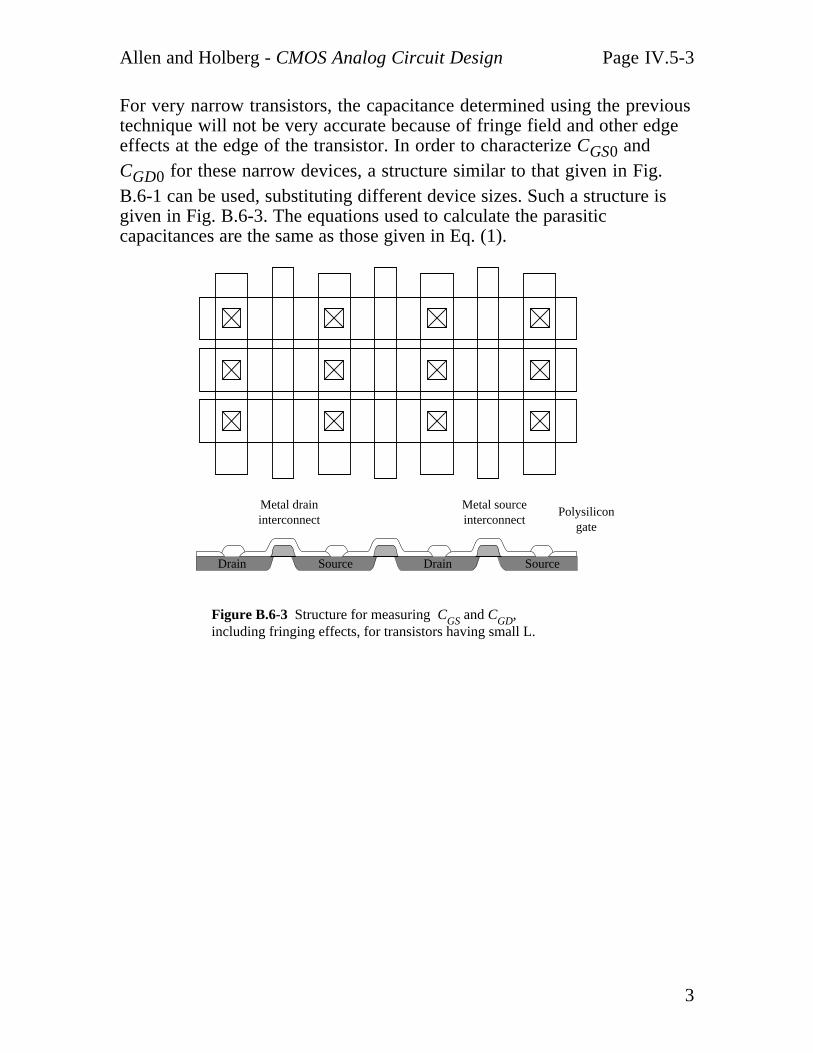
Allen and Holberg - CMOS Analog Circuit Design Page IV.5-3
3
For very narrow transistors, the capacitance determined using the previoustechnique will not be very accurate because of fringe field and other edgeeffects at the edge of the transistor. In order to characterize CGS0 andCGD0 for these narrow devices, a structure similar to that given in Fig.B.6-1 can be used, substituting different device sizes. Such a structure isgiven in Fig. B.6-3. The equations used to calculate the parasiticcapacitances are the same as those given in Eq. (1).
Figure B.6-3 Structure for measuring CGS and CGD, including fringing effects, for transistors having small L.
SourceDrain Drain Source
Metal drain interconnect
Metal source interconnect
Polysilicon gate
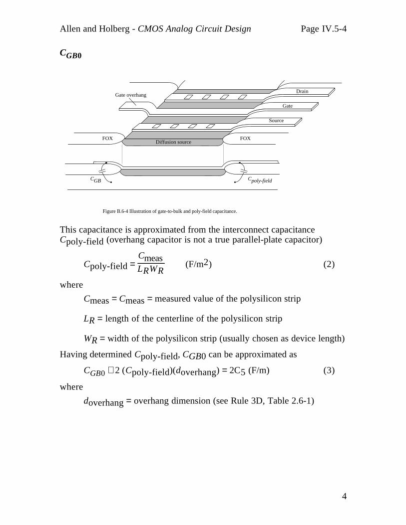
Allen and Holberg - CMOS Analog Circuit Design Page IV.5-4
4
CGB0
Figure B.6-4 Illustration of gate-to-bulk and poly-field capacitance.
CGB Cpoly-field
Diffusion sourceFOX FOX
Source
Gate
DrainGate overhang
This capacitance is approximated from the interconnect capacitanceCpoly-field (overhang capacitor is not a true parallel-plate capacitor)
Cpoly-field = CmeasLRWR
(F/m2) (2)
where
Cmeas = Cmeas = measured value of the polysilicon strip
LR = length of the centerline of the polysilicon strip
WR = width of the polysilicon strip (usually chosen as device length)
Having determined Cpoly-field, CGB0 can be approximated as
CGB0 ≅ 2 (Cpoly-field)(doverhang) = 2C5 (F/m) (3)
where
doverhang = overhang dimension (see Rule 3D, Table 2.6-1)
Allen and Holberg - CMOS Analog Circuit Design Page IV.5-5
5
CBD and CBS
CJ(VJ) = ACJ(0)
1 + VJPB
-MJ + PCJSW(0)
1 + VJPB
-MJSW (4)
where
VJ = the reverse bias voltage across the junction
CJ(VJ) = bottom junction capacitance at VJ
CJSW(VJ) = junction capacitance of sidewall at VJ
A = area of the (bottom) of the capacitor
P = perimeter of the capacitor
PB = bulk junction potential
The constants CJ and MJ can be determined by measuring a largerectangular capacitor structure where the contribution from the sidewallcapacitance is minimal. For such a structure, CJ(VJ) can be approximatedas
CJ(VJ) = ACJ(0)
1 + VJPB
-MJ (5)
This equation can be rewritten in a way that is convenient for linearregression.
log[CJ(VJ)] = (−MJ)log
1 + VJPB + log[ACJ(0)] (6)
Plotting log[CJ(VJ)] versus log[1 + VJ/PB] and determine the slope, −MJ,
and the Y intercept (where Y is the term on the left), Log[ACJ(0)].
Knowing the area of the capacitor, the calculation of the bottom junction
capacitance is straightforward.
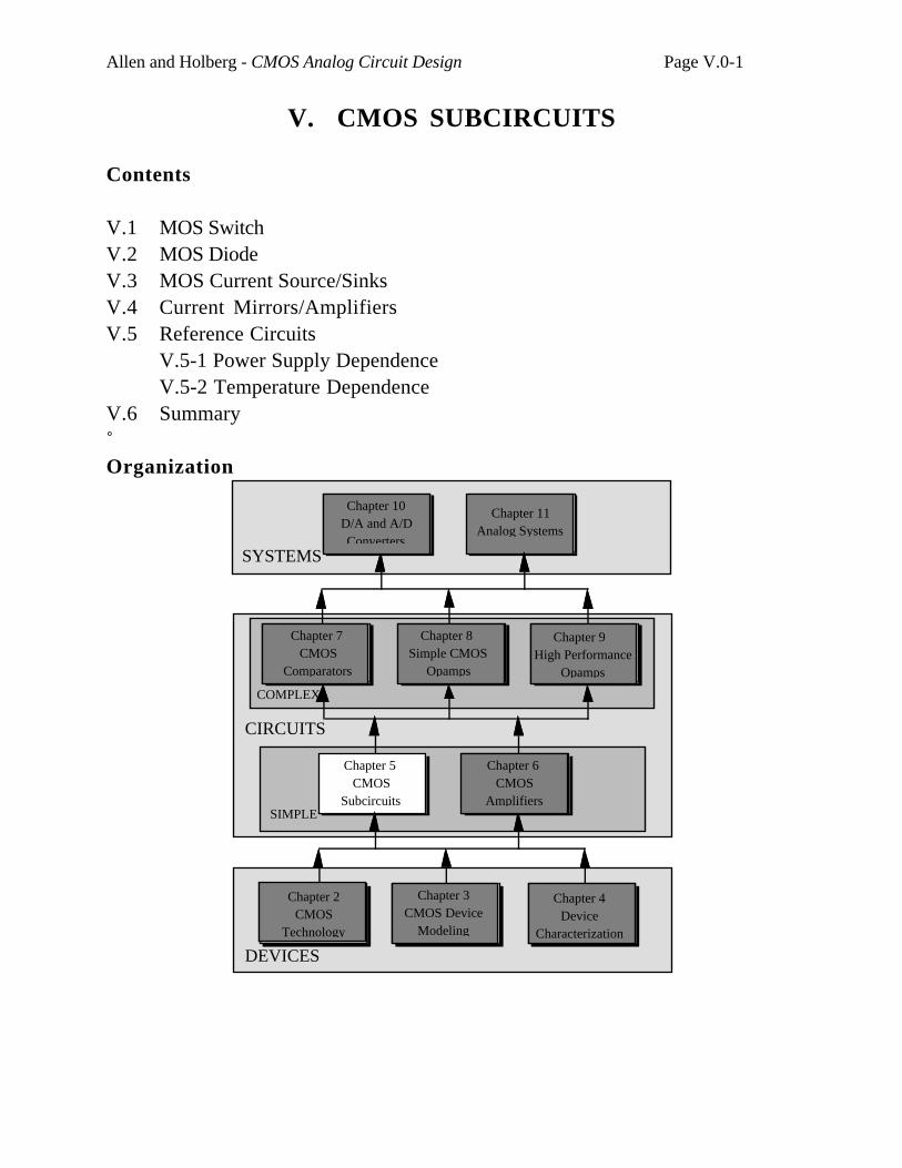
Allen and Holberg - CMOS Analog Circuit Design Page V.0-1
V. CMOS SUBCIRCUITS
Contents
V.1 MOS SwitchV.2 MOS DiodeV.3 MOS Current Source/SinksV.4 Current Mirrors/AmplifiersV.5 Reference Circuits
V.5-1 Power Supply DependenceV.5-2 Temperature Dependence
V.6 Summary Organization
DEVICES
SYSTEMS
CIRCUITS
Chapter 2CMOS
Technology
Chapter 3CMOS Device
Modeling
Chapter 4Device
Characterization
Chapter 7 CMOS
Comparators
Chapter 8 Simple CMOS
Opamps
Chapter 9 High Performance
Opamps
Chapter 5 CMOS
Subcircuits
Chapter 6 CMOS
Amplifiers
Chapter 10D/A and A/D Converters
Chapter 11Analog Systems
SIMPLE
COMPLEX
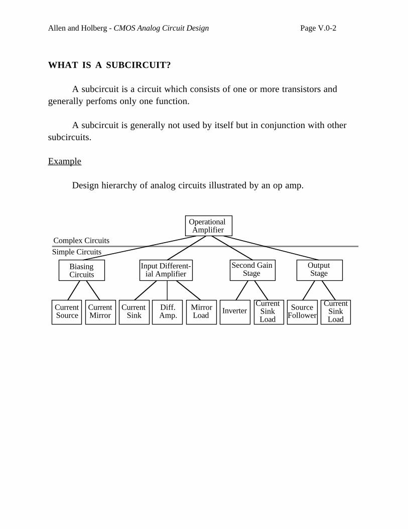
Allen and Holberg - CMOS Analog Circuit Design Page V.0-2
WHAT IS A SUBCIRCUIT?
A subcircuit is a circuit which consists of one or more transistors andgenerally perfoms only one function.
A subcircuit is generally not used by itself but in conjunction with othersubcircuits.
Example
Design hierarchy of analog circuits illustrated by an op amp.
OperationalAmplifier
Biasing Circuits
Input Different- ial Amplifier
Second Gain Stage
Output Stage
Current Source
CurrentMirror
Current Sink
Diff.Amp.
Mirror Load
InverterCurrent
Sink Load
SourceFollower
Current Sink Load
Complex Circuits
Simple Circuits
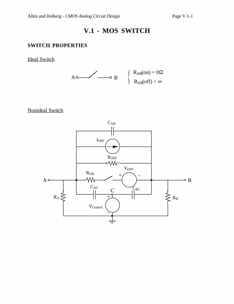
Allen and Holberg - CMOS Analog Circuit Design Page V.1-1
V.1 - MOS SWITCH
SWITCH PROPERTIES
Ideal Switch
A BRAB(on) = 0Ω
RAB(off) = ∞
Nonideal Switch
+ -
IOFF
VOFF
ROFF
RON
RA RB
CAB
+
-VControl
A B
CCAC CBC
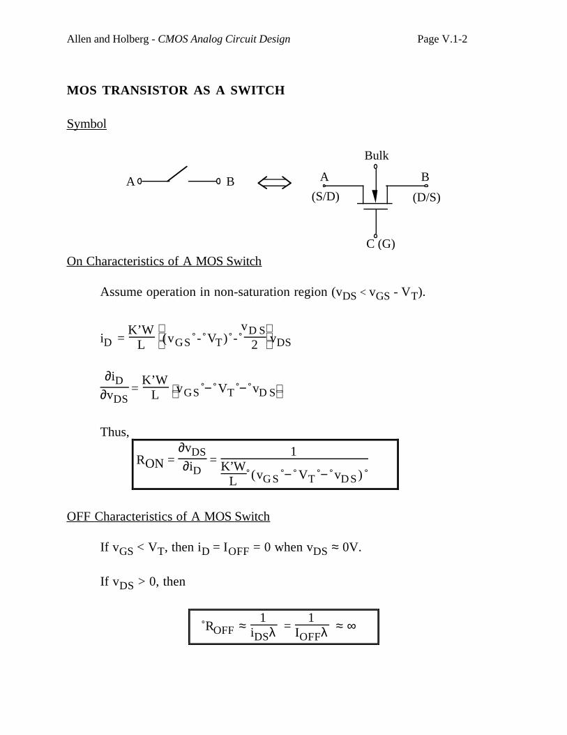
Allen and Holberg - CMOS Analog Circuit Design Page V.1-2
MOS TRANSISTOR AS A SWITCH
Symbol
A B A B
Bulk
C (G)
(S/D) (D/S)
On Characteristics of A MOS Switch
Assume operation in non-saturation region (vDS < vGS - VT).
iD = K’W
L
(vGS - VT) - vD S
2 vDS
∂iD∂vDS
= K’W
L vGS − VT − vD S
Thus,
RON = ∂vDS∂iD
= 1
K’WL (vG S − VT − vD S )
OFF Characteristics of A MOS Switch
If vGS < VT, then iD = IOFF = 0 when vDS ≈ 0V.
If vDS > 0, then
ROFF ≈ 1
iDSλ = 1
IOFFλ ≈ ∞
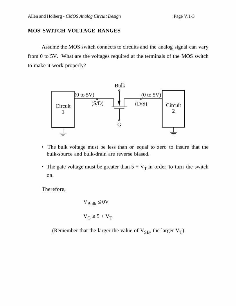
Allen and Holberg - CMOS Analog Circuit Design Page V.1-3
MOS SWITCH VOLTAGE RANGES
Assume the MOS switch connects to circuits and the analog signal can vary
from 0 to 5V. What are the voltages required at the terminals of the MOS switch
to make it work properly?
Bulk
(S/D) (D/S)Circuit1
Circuit2
G
(0 to 5V) (0 to 5V)
• The bulk voltage must be less than or equal to zero to insure that thebulk-source and bulk-drain are reverse biased.
• The gate voltage must be greater than 5 + VT in order to turn the switch
on.
Therefore,
VBulk ≤ 0V
VG ≥ 5 + VT
(Remember that the larger the value of VSB, the larger VT)
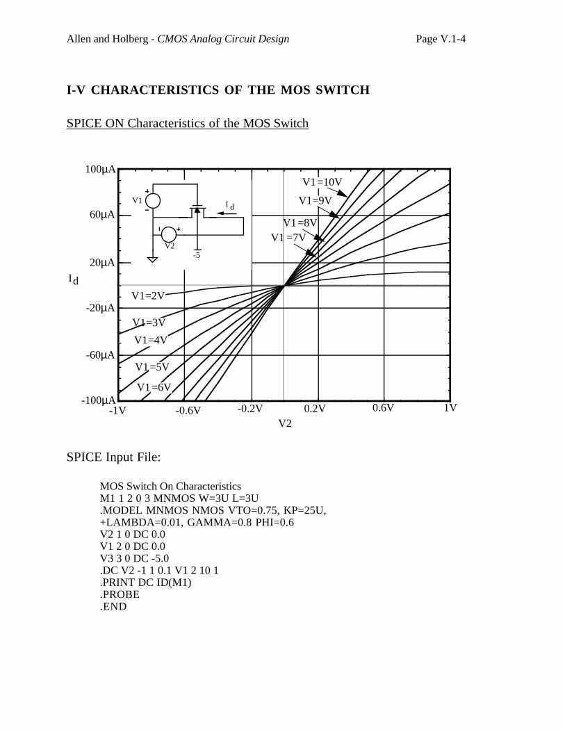
Allen and Holberg - CMOS Analog Circuit Design Page V.1-4
I-V CHARACTERISTICS OF THE MOS SWITCH
SPICE ON Characteristics of the MOS Switch
100µA
60µA
20µA
-20µA
-60µA
-100µA-1V -0.6V -0.2V 0.2V 0.6V 1V
=2V
=3V
=4V
=5V
=10V
=9V
=8V=7V
=6V
V1
V2-5
V1V1
V1
V1
V1
V1
V1
V1
V1
V2
Id
I d
SPICE Input File:
MOS Switch On CharacteristicsM1 1 2 0 3 MNMOS W=3U L=3U.MODEL MNMOS NMOS VTO=0.75, KP=25U,+LAMBDA=0.01, GAMMA=0.8 PHI=0.6V2 1 0 DC 0.0V1 2 0 DC 0.0V3 3 0 DC -5.0.DC V2 -1 1 0.1 V1 2 10 1.PRINT DC ID(M1).PROBE.END
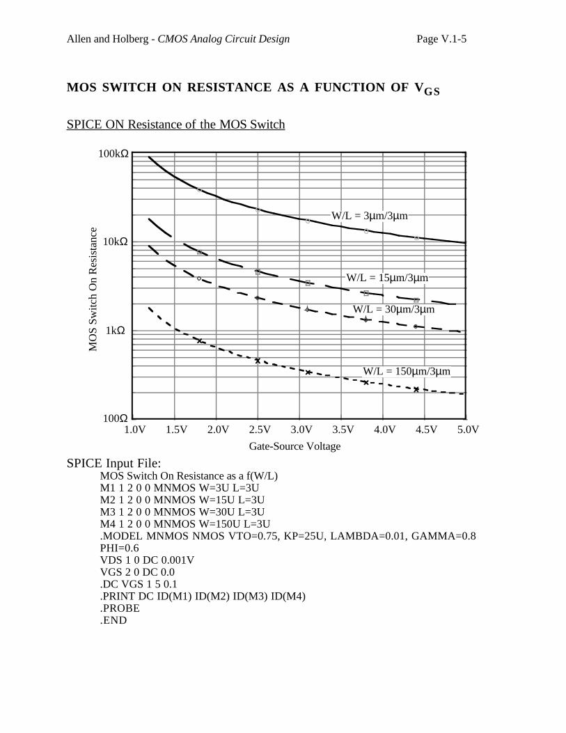
Allen and Holberg - CMOS Analog Circuit Design Page V.1-5
MOS SWITCH ON RESISTANCE AS A FUNCTION OF VGS
SPICE ON Resistance of the MOS Switch
100kΩ
10kΩ
1kΩ
100Ω1.0V 1.5V 2.0V 2.5V 3.0V 3.5V 4.0V 4.5V 5.0V
W/L = 3µm/3µm
W/L = 15µm/3µm
W/L = 30µm/3µm
W/L = 150µm/3µm
MO
S Sw
itch
On
Res
ista
nce
Gate-Source Voltage
SPICE Input File:MOS Switch On Resistance as a f(W/L)M1 1 2 0 0 MNMOS W=3U L=3UM2 1 2 0 0 MNMOS W=15U L=3UM3 1 2 0 0 MNMOS W=30U L=3UM4 1 2 0 0 MNMOS W=150U L=3U.MODEL MNMOS NMOS VTO=0.75, KP=25U, LAMBDA=0.01, GAMMA=0.8PHI=0.6VDS 1 0 DC 0.001VVGS 2 0 DC 0.0.DC VGS 1 5 0.1.PRINT DC ID(M1) ID(M2) ID(M3) ID(M4).PROBE.END
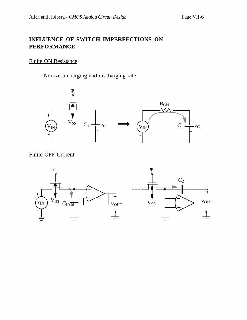
Allen and Holberg - CMOS Analog Circuit Design Page V.1-6
INFLUENCE OF SWITCH IMPERFECTIONS ONPERFORMANCE
Finite ON Resistance
Non-zero charging and discharging rate.
+
-
VSSVIN
C1+
-vC1
φ1
+
-
VIN C1+
-vC1
RON
Finite OFF Current
+
-
+
-
VSS
φ1
CHoldvIN vOUT
+
-
C2
VSS
φ1
vOUT
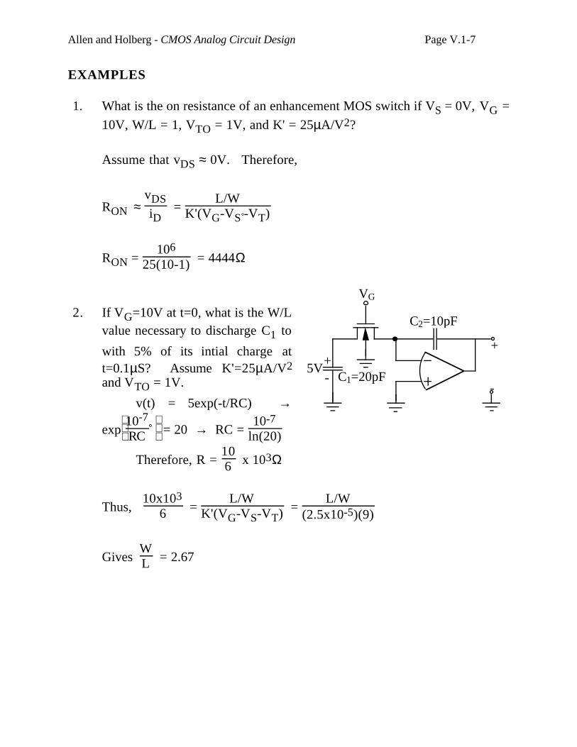
Allen and Holberg - CMOS Analog Circuit Design Page V.1-7
EXAMPLES
1. What is the on resistance of an enhancement MOS switch if VS = 0V, VG =
10V, W/L = 1, VTO = 1V, and K' = 25µA/V2?
Assume that vDS ≈ 0V. Therefore,
RON ≈ vDSiD
= L/W
K'(VG-VS -VT)
RON = 106
25(10-1) = 4444Ω
2. If VG=10V at t=0, what is the W/Lvalue necessary to discharge C1 to
with 5% of its intial charge att=0.1µS? Assume K'=25µA/V2
and VTO = 1V.
v(t) = 5exp(-t/RC) →
exp
10-7
RC = 20 → RC = 10-7
ln(20)
Therefore, R = 106 x 103Ω
Thus, 10x103
6 = L/W
K'(VG-VS-VT) = L/W
(2.5x10⁻⁵)(9)
Gives WL = 2.67
+
-
+-
5VC1=20pF
C2=10pF
VG
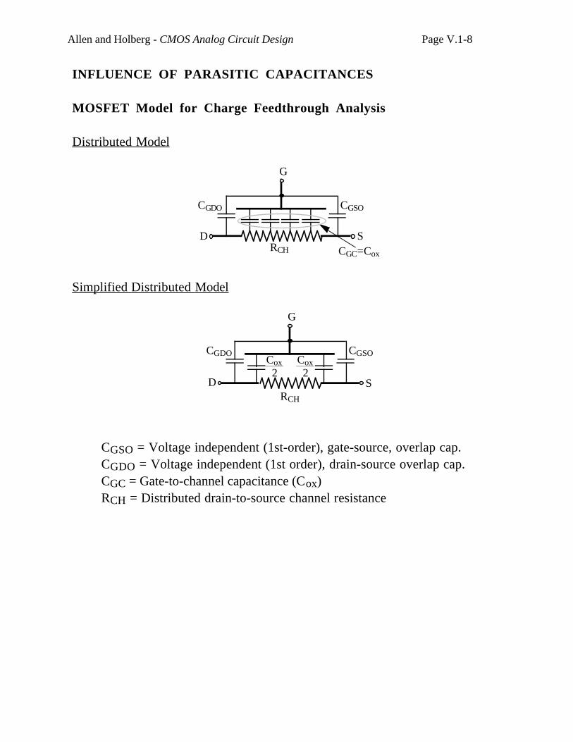
Allen and Holberg - CMOS Analog Circuit Design Page V.1-8
INFLUENCE OF PARASITIC CAPACITANCES
MOSFET Model for Charge Feedthrough Analysis
Distributed Model
G
D S
CGDO CGSO
CGC=CoxRCH
Simplified Distributed Model
G
D S
CGDO CGSOCox2
Cox2
RCH
CGSO = Voltage independent (1st-order), gate-source, overlap cap.CGDO = Voltage independent (1st order), drain-source overlap cap.CGC = Gate-to-channel capacitance (Cox)RCH = Distributed drain-to-source channel resistance
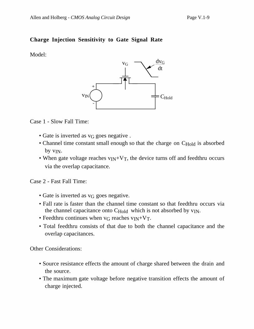
Allen and Holberg - CMOS Analog Circuit Design Page V.1-9
Charge Injection Sensitivity to Gate Signal Rate
Model:
+
-
vIN
vG
CHold
dvG
dt
Case 1 - Slow Fall Time:
• Gate is inverted as vG goes negative .• Channel time constant small enough so that the charge on CHold is absorbed
by vIN.• When gate voltage reaches vIN+VT, the device turns off and feedthru occurs
via the overlap capacitance.
Case 2 - Fast Fall Time:
• Gate is inverted as vG goes negative.
• Fall rate is faster than the channel time constant so that feedthru occurs viathe channel capacitance onto CHold which is not absorbed by vIN.
• Feedthru continues when vG reaches vIN+VT.
• Total feedthru consists of that due to both the channel capacitance and theoverlap capacitances.
Other Considerations:
• Source resistance effects the amount of charge shared between the drain andthe source.
• The maximum gate voltage before negative transition effects the amount ofcharge injected.
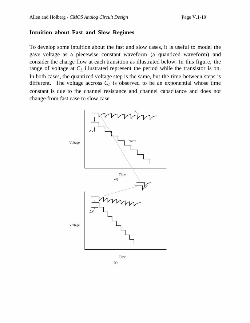
Allen and Holberg - CMOS Analog Circuit Design Page V.1-10
Intuition about Fast and Slow Regimes
To develop some intuition about the fast and slow cases, it is useful to model thegave voltage as a piecewise constant waveform (a quantized waveform) andconsider the charge flow at each transition as illustrated below. In this figure, therange of voltage at CL illustrated represent the period while the transistor is on.
In both cases, the quantized voltage step is the same, but the time between steps isdifferent. The voltage accross CL is observed to be an exponential whose time
constant is due to the channel resistance and channel capacitance and does notchange from fast case to slow case.
Figure 4.1-10 (a) Illustration of slow ramp and (b) fast ramp using a quantized voltage ramp to illustrate the effects due to the time constant of the channel resistance and capacitance.
(d)
(e)
∆V
∆V
Time
Voltage
Time
Voltage
vGATE
vCL
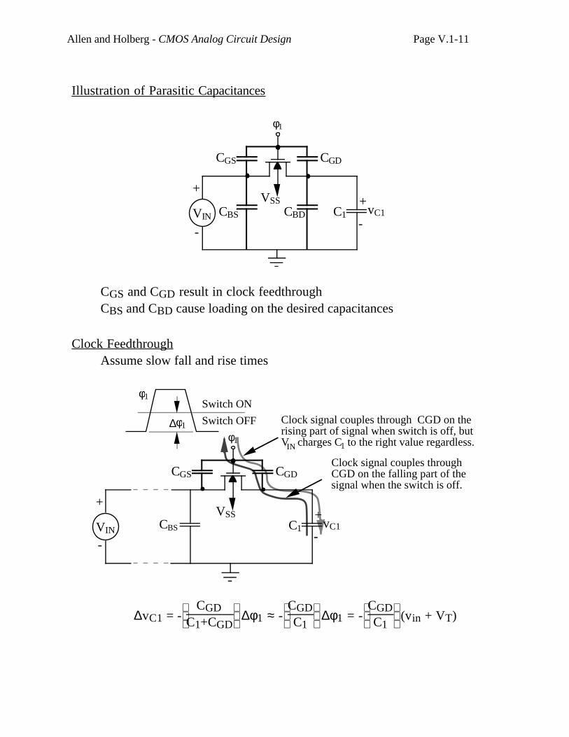
Allen and Holberg - CMOS Analog Circuit Design Page V.1-11
Illustration of Parasitic Capacitances
+
-
VSS
VIN C1+
-vC1
φ1
CGS CGD
CBS CBD
CGS and CGD result in clock feedthroughCBS and CBD cause loading on the desired capacitances
Clock Feedthrough Assume slow fall and rise times
+
-
VSS
VIN C1+
-vC1
φ1
CGS CGD
Clock signal couples through CGD on the rising part of signal when switch is off, butV charges C to the right value regardless.
Clock signal couples through CGD on the falling part of the signal when the switch is off.
CBS
IN 1
φ1Switch ON
Switch OFF∆φ1
∆vC1 = -
CGD
C1+CGD ∆φ1 ≈ -
CGD
C1 ∆φ1 = -
CGD
C1 (vin + VT)
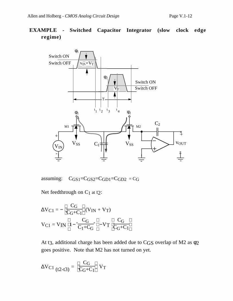
Allen and Holberg - CMOS Analog Circuit Design Page V.1-12
EXAMPLE - Switched Capacitor Integrator (slow clock edgeregime)
+
-
VSS
φ1
+
-
VSS
φ2
C2
C1vOUT
VIN
φ1
Switch ON
Switch OFF
φ2
vIN+VT
T
VT
Switch ONSwitch OFF
t1 t 2 t 3 t 4
M1 M2
assuming: CGS1=CGS2=CGD1=CGD2 = CG
Net feedthrough on C1 at t2:
∆VC1 = −
CG
CG+C1 (VIN + VT)
VC1 = VIN
1− CG
C1+CG −VT
CG
CG+C1
At t3, additional charge has been added due to CGS overlap of M2 as φ2goes positive. Note that M2 has not turned on yet.
∆VC1 (t2-t3) =
CG
CG+C1 VT
Allen and Holberg - CMOS Analog Circuit Design Page V.1-13
Giving at the end of t3 (before M2 turns on):
VC1 = VIN
1−CG
C1+CG
Once M2 turns on (at t+3 ), all of the charge on C1 is transferred to C2.
∆VO = −VC1
C1
C2 = −VIN
C1
C2
1− CG
C1+CG
Between times at t+3 and t4 additional charge is transferred to C1 from the
channel capacitance of M2.
∆VO (t3-t4)= −
Cch
C2 (Vclk −VT)
The final change in Vout is:
∆VO = −VIN
C1
C2
1−CG
C1+CG −
Cch
C2 (Vclk − VT)
Ideally the output voltage change is −VIN
C1
C2 so the error due to charge
feedthrough is:
∆VO (error) = VIN
C1
C2
CG
C1+CG −
Cch
C2 (Vclk − VT)
Allen and Holberg - CMOS Analog Circuit Design Page V.1-14
Rigorous Quantitative Analysis of Fast and Slow Regimes
Consider the gate voltage traversing from VH to VL (e.g., 5.0 volts to 0.0 volts,respectively) described in the time domain as
vG = VH − Ut (3)
When operating in the slow regime defined by the relationship
β V 2HT
2CL >> U (4)
where VHT is defined as
VHT = VH − VS − VT (5)
the error (the difference between the desired voltage VS and the actual voltage,VCL) due to charge injection can be described as
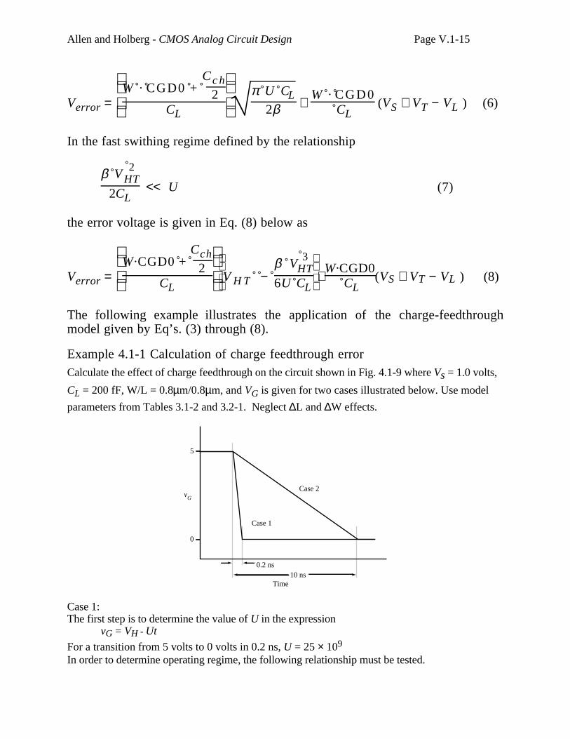
Allen and Holberg - CMOS Analog Circuit Design Page V.1-15
Verror =
W · CGD0 +
Cc h2
CL
π U CL2β +
W · C G D 0 CL
(VS + VT − VL ) (6)
In the fast swithing regime defined by the relationship
β V 2HT
2CL << U (7)
the error voltage is given in Eq. (8) below as
Verror =
W·CGD0 +
Cch2
CL
V H T − β V
3HT
6U CL+W·CGD0
CL(VS + VT − VL ) (8)
The following example illustrates the application of the charge-feedthroughmodel given by Eq’s. (3) through (8).
Example 4.1-1 Calculation of charge feedthrough errorCalculate the effect of charge feedthrough on the circuit shown in Fig. 4.1-9 where Vs = 1.0 volts,
CL = 200 fF, W/L = 0.8µm/0.8µm, and VG is given for two cases illustrated below. Use model
parameters from Tables 3.1-2 and 3.2-1. Neglect ∆L and ∆W effects.
Time
vG
0
5
0.2 ns10 ns
Case 1
Case 2
Case 1:The first step is to determine the value of U in the expression
vG = VH - Ut
For a transition from 5 volts to 0 volts in 0.2 ns, U = 25 × 109
In order to determine operating regime, the following relationship must be tested.
Allen and Holberg - CMOS Analog Circuit Design Page V.1-16
β V 2HT
2CL >> U for slow or
β V 2HT
2CL << U for fast
Observin g that there is a backbias on the transistor switch effecting VT, VHT isVHT = VH - VS - VT = 5 - 1 - 0.887 = 3.113
giving
β V 2HT
2CL =
110×10-6× 3.1132
2 × 200f = 2.66 × 10⁹ << 25 × 109 thus fast regime.
Applying Eq. (8) for the fast regime yields
Verror =
176×10-18 + 1.58×10⁻¹⁵
2
200×10-15
3.113 - 3.32×10⁻³
30×10-3 +176×10-18
200×10-15 (5 + 0.887 - 0)
Verror = 19.7 mV
Case 2:The first step is to determine the value of U in the expression
v G = VH - Ut
For a transition from 5 volts to 0 volts in 10 ns, U = 5 × 10⁸ thus indicating the slow regimeaccording to the following test
2.66 × 10⁹ >> 5 × 10⁸
Verror =
176×10-18 + 1.58×10⁻¹⁵
2
200×10-15 314×10-6
220×10-6 + 176×10-18
200×10-15 (5 + 0.887 - 0 )
Verror = 10.95 mV
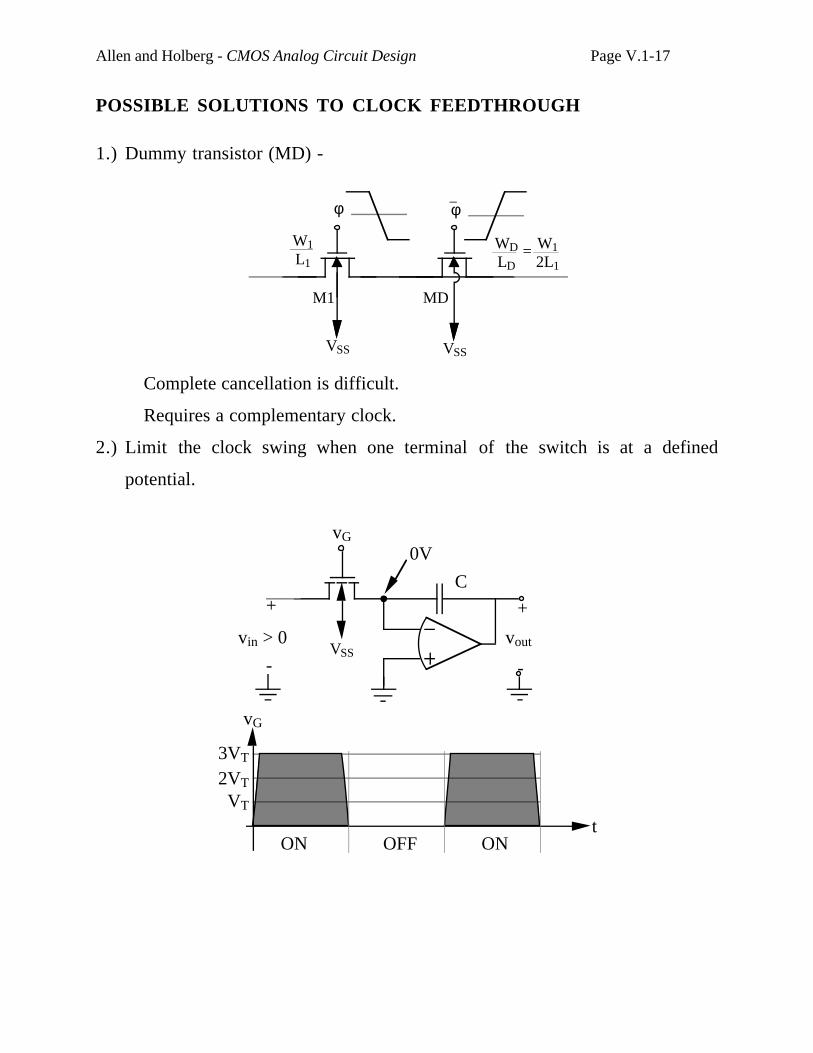
Allen and Holberg - CMOS Analog Circuit Design Page V.1-17
POSSIBLE SOLUTIONS TO CLOCK FEEDTHROUGH
1.) Dummy transistor (MD) -
VSS VSS
φ φ
W1L1
WDLD
= W12L1
M1 MD
Complete cancellation is difficult.
Requires a complementary clock.
2.) Limit the clock swing when one terminal of the switch is at a defined
potential.
+
-VSS
vin > 0
0V
vout
+
-
C
vG
VT
2VT
3VT
vG
ON OFF ONt
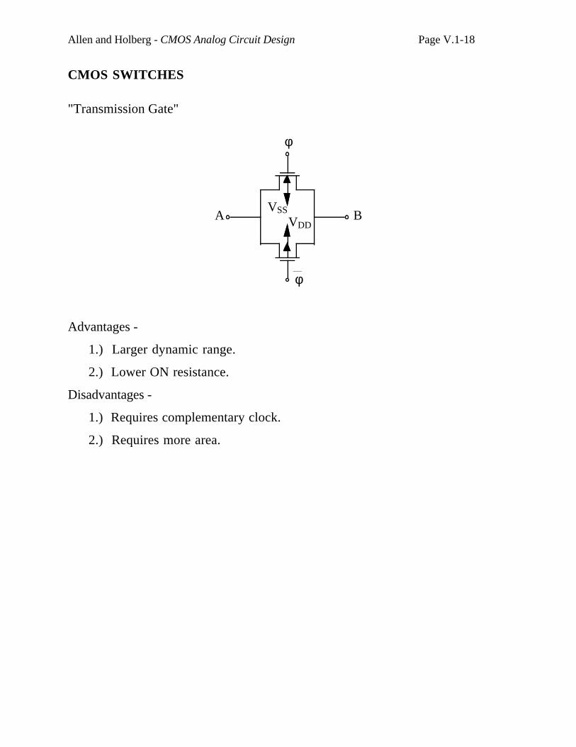
Allen and Holberg - CMOS Analog Circuit Design Page V.1-18
CMOS SWITCHES
"Transmission Gate"
VSS
VDDA B
φ
φ
Advantages -
1.) Larger dynamic range.
2.) Lower ON resistance.
Disadvantages -
1.) Requires complementary clock.
2.) Requires more area.
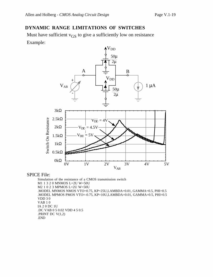
Allen and Holberg - CMOS Analog Circuit Design Page V.1-19
DYNAMIC RANGE LIMITATIONS OF SWITCHESMust have sufficient vGS to give a sufficiently low on resistance
Example:
VDD
A B
VDD
50µ2µ
50µ2µ
1 µA+
-
VAB
0kΩ
0.5kΩ
1kΩ
1.5kΩ
2kΩ
2.5kΩ
3kΩ
Switc
h O
n R
esis
tanc
e
0V 1V 2V 3V 4V 5VVAB
VDD = 5V
VDD = 4.5V
VDD = 4V
SPICE File:Simulation of the resistance of a CMOS transmission switchM1 1 3 2 0 MNMOS L=2U W=50UM2 1 0 2 3 MPMOS L=2U W=50U.MODEL MNMOS NMOS VTO=0.75, KP=25U,LAMBDA=0.01, GAMMA=0.5, PHI=0.5.MODEL MPMOS PMOS VTO=-0.75, KP=10U,LAMBDA=0.01, GAMMA=0.5, PHI=0.5VDD 3 0VAB 1 0IA 2 0 DC 1U.DC VAB 0 5 0.02 VDD 4 5 0.5.PRINT DC V(1,2).END
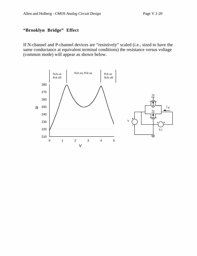
Allen and Holberg - CMOS Analog Circuit Design Page V.1-20
“Brooklyn Bridge” Effect
If N-channel and P-channel devices are “resistively” scaled (i.e., sized to have thesame conductance at equivalent terminal conditions) the resistance versus voltage(common mode) will appear as shown below.
280
270
260
250
240
230
220
210543210
R
V
Nch onPch off
Pch onNch off
Nch on; Pch on
V
I d
0.1
5v
5v
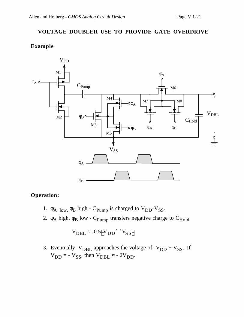
Allen and Holberg - CMOS Analog Circuit Design Page V.1-21
VOLTAGE DOUBLER USE TO PROVIDE GATE OVERDRIVE
Example
CHold
VDBL
+
-φA
φA
φA
φA
φB
φB φB
CPump
M1
M2
M3
M4
M5
M6
M7 M8
VDD
VSS
φB
φA
Operation:
1. φA low, φB high - CPump is charged to VDD-VSS.
2. φA high, φB low - CPump transfers negative charge to CHold
VDBL ≈ -0.5 VDD - VS S
3. Eventually, VDBL approaches the voltage of -VDD + VSS. If VDD = - VSS, then VDBL ≈ - 2VDD.

Allen and Holberg - CMOS Analog Circuit Design Page V.1-22
SUMMARY OF MOS SWITCHES
• Symmetrical switching characteristics
• High OFF resistance
• Moderate ON resistance (OK for most applications)
• Clock feedthrough is proportional to size of switch (W) and inversely
proportional to switching capacitors.
• Complementary switches help increase dynamic range.
• As power supply reduces, switches become more difficult to fully turn
on.
• Switches contribute a kT/C noise which folds back into the baseband.
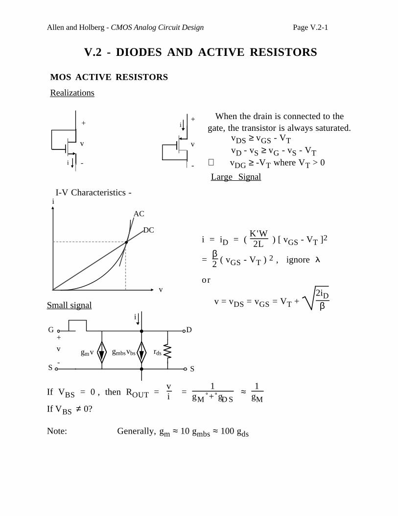
Allen and Holberg - CMOS Analog Circuit Design Page V.2-1
V.2 - DIODES AND ACTIVE RESISTORS
MOS ACTIVE RESISTORS
Realizations
When the drain is connected to thegate, the transistor is always saturated.
vDS ≥ vGS - VTvD - vS ≥ vG - vS - VT
∴ vDG ≥ -VT where VT > 0
Large Signal
I-V Characteristics -i
v
AC
DC
Small signal
D
S
i
G+
-
gmbsvbsv rds
S
gmv
If VBS = 0 , then ROUT = vi =
1gM + gD S
≈ 1
gM
If VBS ≠ 0?
Note: Generally, gm ≈ 10 gmbs ≈ 100 gds
+
-
v
i
+
-
v
i
i = iD = ( K'W2L ) [ vGS - VT ]2
= β2 ( vGS - VT ) 2 , ignore λ
or
v = vDS = vGS = VT + 2iDβ
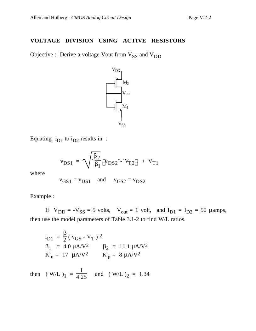
Allen and Holberg - CMOS Analog Circuit Design Page V.2-2
VOLTAGE DIVISION USING ACTIVE RESISTORS
Objective : Derive a voltage Vout from VSS and VDD
VDD
VSS
Vout
M2
M1
Equating iD1 to iD2 results in :
vDS1 = β2β1
vDS2 - VT 2 + VT1
where vGS1 = vDS1 and vGS2 = vDS2
Example :
If VDD = -VSS = 5 volts, Vout = 1 volt, and ID1 = ID2 = 50 µamps,
then use the model parameters of Table 3.1-2 to find W/L ratios.
iD1 = β2 ( vGS - VT ) 2
β1 = 4.0 µA/V2 β2 = 11.1 µA/V2
K'n = 17 µA/V2 K'p = 8 µA/V2
then ( W/L )1 = 1
4.25 and ( W/L )2 = 1.34
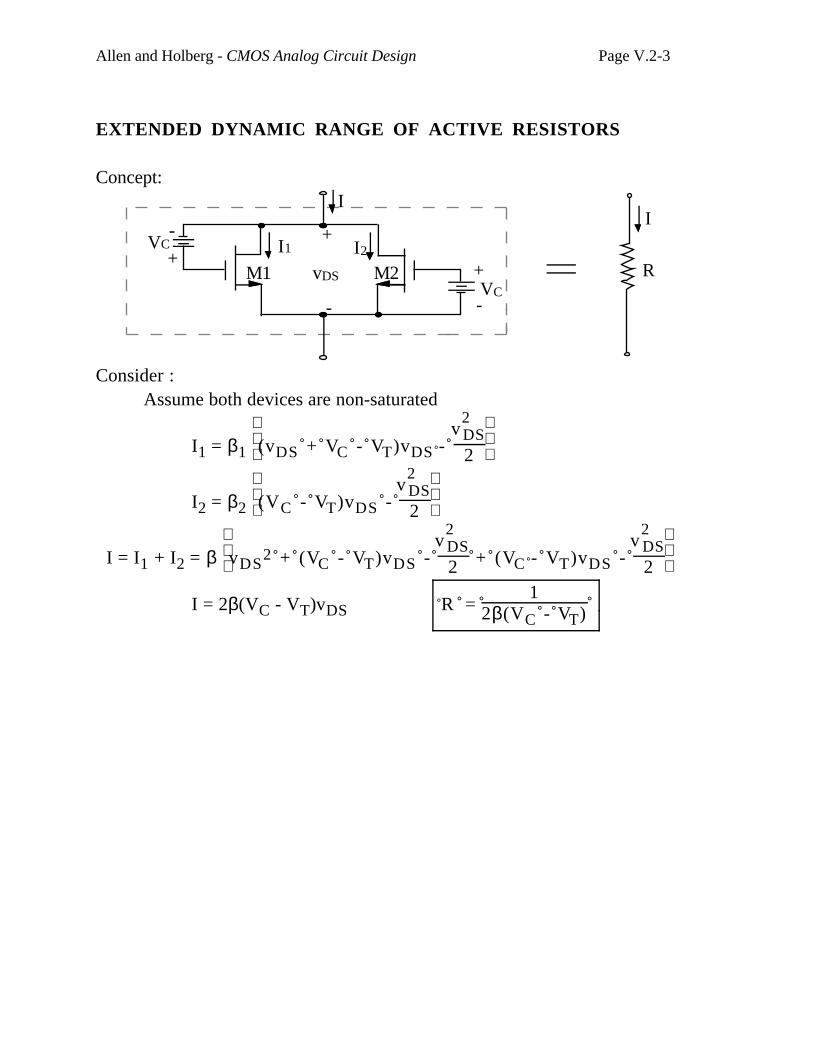
Allen and Holberg - CMOS Analog Circuit Design Page V.2-3
EXTENDED DYNAMIC RANGE OF ACTIVE RESISTORS
Concept:
I1 I2+
-
vDSM1 M2
VC+
-
-
+VC
I
R
I
Consider :Assume both devices are non-saturated
I1 = β1
(vDS + VC - VT)vDS - v
2DS2
I2 = β2
(VC - VT)vDS - v
2DS2
I = I1 + I2 = β
vDS2 + (VC - VT)vDS -
v2DS2 + (VC - VT)vDS -
v2DS2
I = 2β(VC - VT)vDS R = 1
2β(VC - VT)
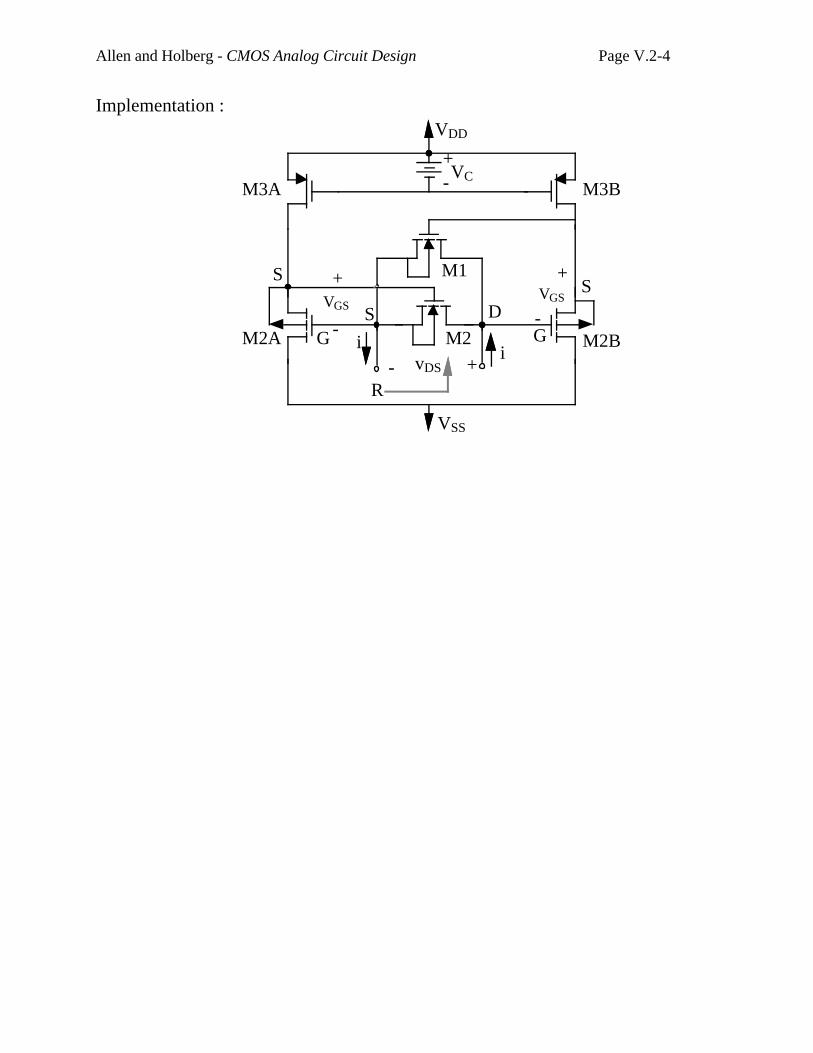
Allen and Holberg - CMOS Analog Circuit Design Page V.2-4
Implementation :
M3B
M2B
M1
M2
M3A
M2A
+-
VDD
VC+-
VSS
S
i
D
ivDS
R
S
G G
S+
-
+
-VGS
VGS
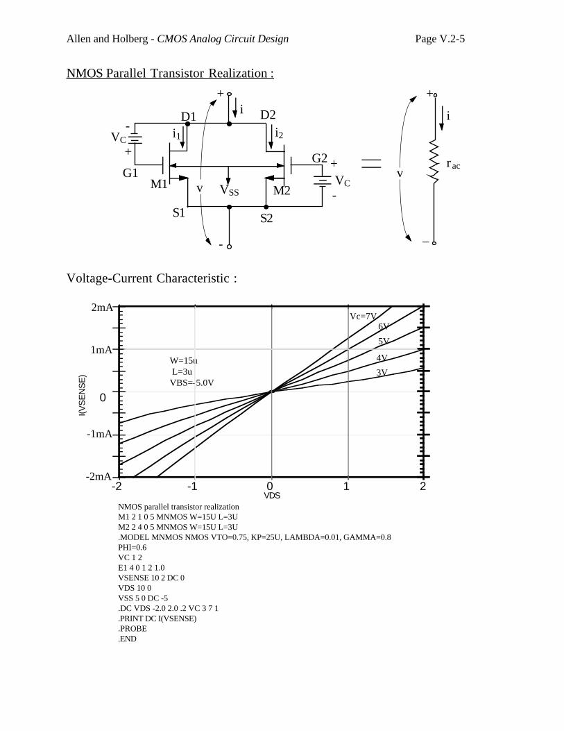
Allen and Holberg - CMOS Analog Circuit Design Page V.2-5
NMOS Parallel Transistor Realization :
+
-
M1 M2
VC
+
-
-
+VC
ii
VSS
S1
G1
D1 D2
v
S2
G2v
+
_
rac
i1 i2
Voltage-Current Characteristic :
Vc=7V
VDS
0
I(VS
EN
SE
)
-2 -1 0 1 2
2mA
1mA
-1mA
-2mA
W=15u L=3uVBS=-5.0V
NMOS parallel transistor realizationM1 2 1 0 5 MNMOS W=15U L=3UM2 2 4 0 5 MNMOS W=15U L=3U.MODEL MNMOS NMOS VTO=0.75, KP=25U, LAMBDA=0.01, GAMMA=0.8 PHI=0.6VC 1 2E1 4 0 1 2 1.0VSENSE 10 2 DC 0VDS 10 0 VSS 5 0 DC -5.DC VDS -2.0 2.0 .2 VC 3 7 1.PRINT DC I(VSENSE).PROBE.END
6V
5V
4V
3V
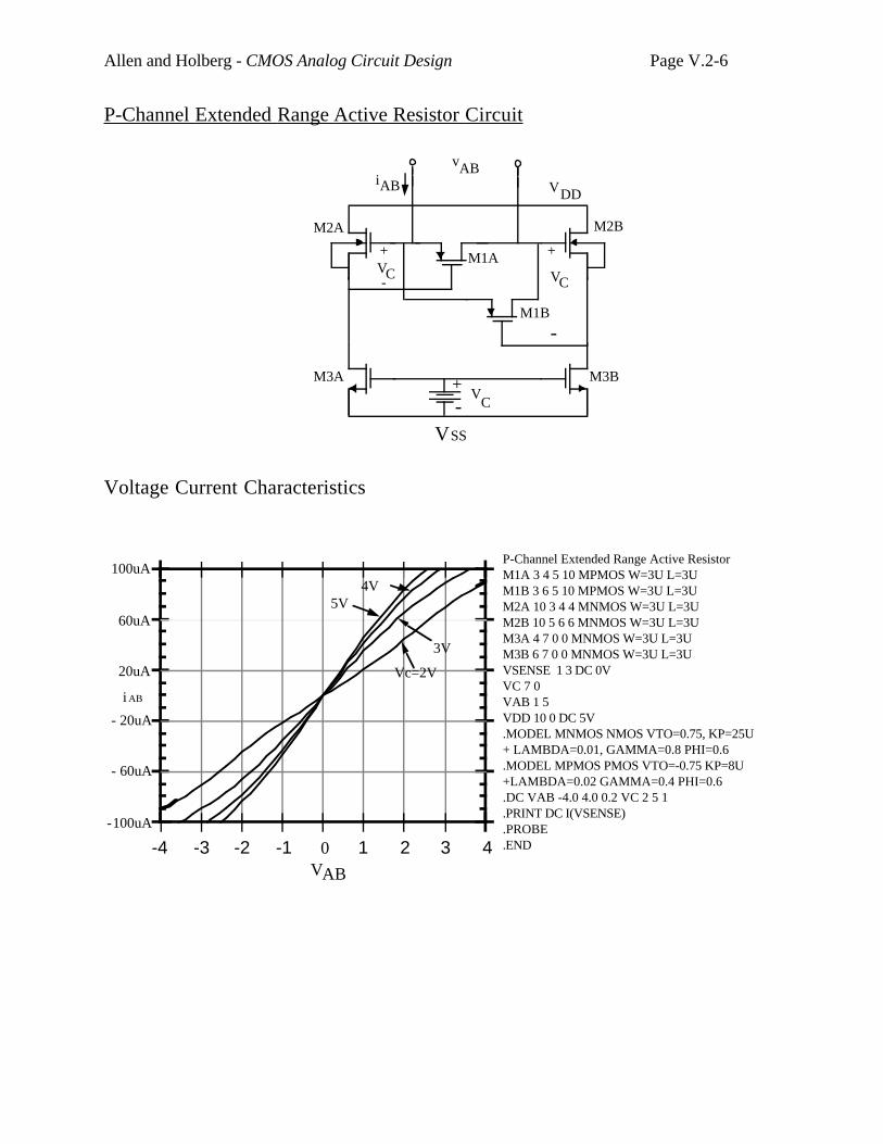
Allen and Holberg - CMOS Analog Circuit Design Page V.2-6
P-Channel Extended Range Active Resistor Circuit
VDD
VSS
M2A
M3A
M1A
M1B
M2B
M3B
iAB
VC
+-
VC
+
-
+
-
VC
ABv
Voltage Current Characteristics
P-Channel Extended Range Active ResistorM1A 3 4 5 10 MPMOS W=3U L=3UM1B 3 6 5 10 MPMOS W=3U L=3U M2A 10 3 4 4 MNMOS W=3U L=3UM2B 10 5 6 6 MNMOS W=3U L=3UM3A 4 7 0 0 MNMOS W=3U L=3UM3B 6 7 0 0 MNMOS W=3U L=3UVSENSE 1 3 DC 0VVC 7 0VAB 1 5VDD 10 0 DC 5V.MODEL MNMOS NMOS VTO=0.75, KP=25U+ LAMBDA=0.01, GAMMA=0.8 PHI=0.6.MODEL MPMOS PMOS VTO=-0.75 KP=8U+LAMBDA=0.02 GAMMA=0.4 PHI=0.6.DC VAB -4.0 4.0 0.2 VC 2 5 1.PRINT DC I(VSENSE).PROBE.END
VAB
i AB
-4 -3 -2 -1 1 2 3 4
100uA
60uA
20uA
100uA
20uA
60uA
-
-
-
0
Vc=2V
3V
4V5V
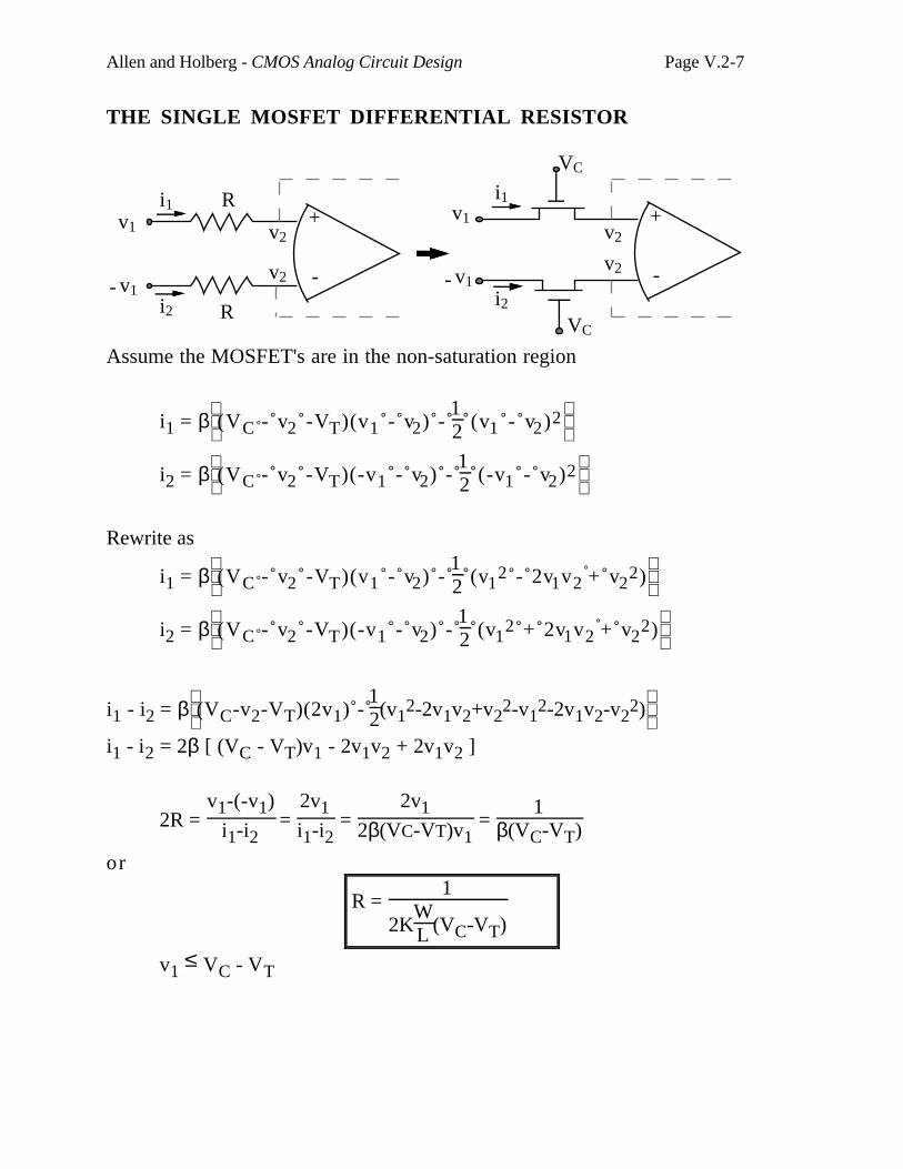
Allen and Holberg - CMOS Analog Circuit Design Page V.2-7
THE SINGLE MOSFET DIFFERENTIAL RESISTOR
+
-
R
R-
+
-
v1
v1
i1
i2
v2
v2 -
v1
v1
i1
i2
v2
v2
VC
VC
Assume the MOSFET's are in the non-saturation region
i1 = β
(VC - v2 -VT)(v1 - v2) - 12 (v1 - v2)2
i2 = β
(VC - v2 -VT)(-v1 - v2) - 12 (-v1 - v2)2
Rewrite as
i1 = β
(VC - v2 -VT)(v1 - v2) - 12 (v1
2 - 2v1v2 + v2
2)
i2 = β
(VC - v2 -VT)(-v1 - v2) - 12 (v1
2 + 2v1v2 + v2
2)
i1 - i2 = β
(VC-v2-VT)(2v1) - 12(v1
2-2v1v2+v22-v1
2-2v1v2-v22)
i1 - i2 = 2β [ (VC - VT)v1 - 2v1v2 + 2v1v2 ]
2R = v1-(-v1)
i1-i2 =
2v1i1-i2
= 2v1
2β(VC-VT)v1 =
1β(VC-VT)
or
R = 1
2KWL (VC-VT)
v1 ≤ VC - VT
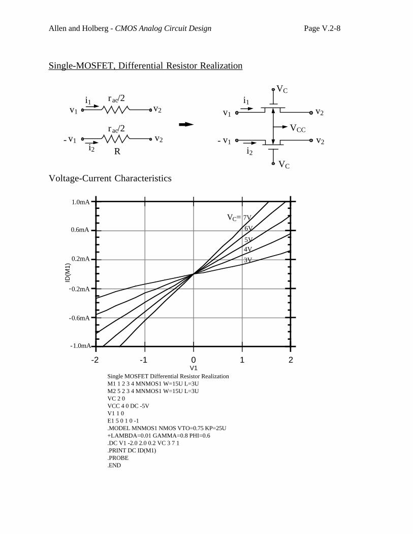
Allen and Holberg - CMOS Analog Circuit Design Page V.2-8
Single-MOSFET, Differential Resistor Realization
R-
rac/2
rac/2-
VCC
VC
VC
i2 i2
i1 i1v1
v1
v1
v1
v2
v2
v2
v2
Voltage-Current Characteristics
Single MOSFET Differential Resistor Realization M1 1 2 3 4 MNMOS1 W=15U L=3UM2 5 2 3 4 MNMOS1 W=15U L=3UVC 2 0 VCC 4 0 DC -5VV1 1 0 E1 5 0 1 0 -1.MODEL MNMOS1 NMOS VTO=0.75 KP=25U+LAMBDA=0.01 GAMMA=0.8 PHI=0.6.DC V1 -2.0 2.0 0.2 VC 3 7 1.PRINT DC ID(M1).PROBE.END
-2
ID(M
1)
-1 0 1V1
2
0.6mA
1.0mA
0.2mA
0.2mA
0.6mA
1.0mA
-
-
-
VC= 7V
6V
5V
4V
3V
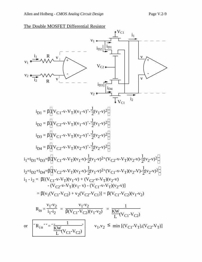
Allen and Holberg - CMOS Analog Circuit Design Page V.2-9
The Double MOSFET Differential Resistor
+
-
R
R
+
-
v
v
VC1
VC1
VC2
i2
i1
iD1iD2
iD3iD4
v2
i1
i2
v1
v2
v1
v
v
iD1 = β
(VC1-v-VT)(v1-v) - 12(v1-v)2
iD2 = β
(VC2-v-VT)(v1-v) - 12(v1-v)2
iD3 = β
(VC1-v-VT)(v2-v) - 12(v2-v)2
iD4 = β
(VC2-v-VT)(v2-v) - 12(v2-v)2
i1=iD1+iD3=β
(VC1-v-VT)(v1-v)-12(v1-v)2+(VC2-v-VT)(v2-v)-
12(v2-v)2
i2=iD2+iD4=β
(VC2-v-VT)(v1-v)-12(v1-v)2+(VC1-v-VT)(v2-V)-
12(v2-v)2
i1 - i2 = β[(VC1-v-VT)(v1-v) + (VC2-v-VT)(v2-v) - (VC2-v-VT)(v1- v) - (VC1-v-VT)(v2-v)]
= β[v1(VC1-VC2) + v2(VC2-VC1)] = β(VC1-VC2)(v1-v2)
Rin = v1-v2i1-i2 =
v1-v2β(VC1-VC2)(v1-v2) =
1KWL (VC1-VC2)
or R i n = 1
KWL (VC1-VC2)
v1,v2 ≤ min [(VC1-VT),(VC2-VT)]
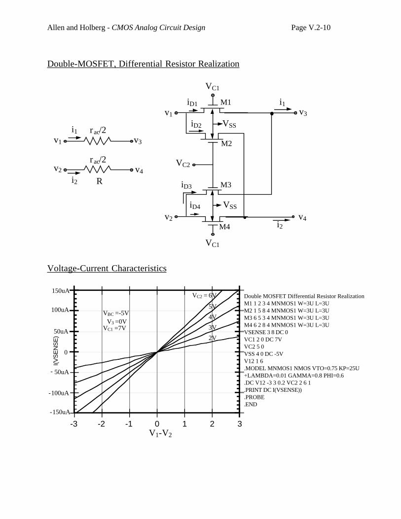
Allen and Holberg - CMOS Analog Circuit Design Page V.2-10
Double-MOSFET, Differential Resistor Realization
R
rac/2
rac/2
VC1
VC1
VC2
VSS
VSS
M1
M2
M3
M4
v2
v1 v3
v4
i1
i2
v2
v1 v3
v4
i1
i2
iD2
iD1
iD3
iD4
Voltage-Current Characteristics
V1-V2
-3 -2 -1 0 1 2 3
VC2 = 6V
5V
4V
3V
2V
VBC =-5VV3 =0V
VC1 =7V
I(VS
EN
SE
)
150uA
100uA
50uA
0
50uA-
100uA-
150uA-
Double MOSFET Differential Resistor RealizationM1 1 2 3 4 MNMOS1 W=3U L=3UM2 1 5 8 4 MNMOS1 W=3U L=3UM3 6 5 3 4 MNMOS1 W=3U L=3UM4 6 2 8 4 MNMOS1 W=3U L=3UVSENSE 3 8 DC 0VC1 2 0 DC 7VVC2 5 0 VSS 4 0 DC -5VV12 1 6 .MODEL MNMOS1 NMOS VTO=0.75 KP=25U+LAMBDA=0.01 GAMMA=0.8 PHI=0.6.DC V12 -3 3 0.2 VC2 2 6 1 .PRINT DC I(VSENSE)).PROBE.END
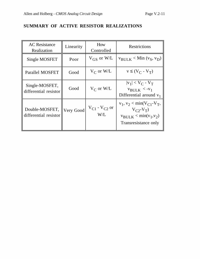
Allen and Holberg - CMOS Analog Circuit Design Page V.2-11
SUMMARY OF ACTIVE RESISTOR REALIZATIONS
AC ResistanceRealization
Linearity HowControlled
Restrictions
Single MOSFET Poor VGS or W/L vBULK < Min (vS, vD)
Parallel MOSFET Good VC or W/L v ≤ (VC - VT)
Single-MOSFET,differential resistor
Good VC or W/L|v1| < VC - VTvBULK < -v1
Differential around v1
Double-MOSFET,differential resistor
Very GoodVC1 - VC2 or
W/L
v1, v2 < min(VC1-VT, VC2-VT)
vBULK < min(v1,v2)
Transresistance only
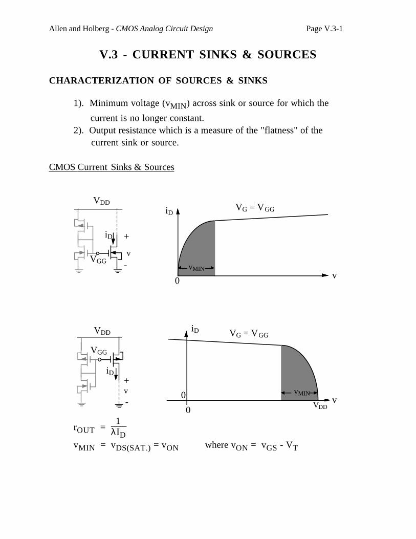
Allen and Holberg - CMOS Analog Circuit Design Page V.3-1
V.3 - CURRENT SINKS & SOURCES
CHARACTERIZATION OF SOURCES & SINKS
1). Minimum voltage (vMIN) across sink or source for which the
current is no longer constant.2). Output resistance which is a measure of the "flatness" of the current sink or source.
CMOS Current Sinks & Sources
v
VG = VGG
0
iD
vMIN
v
VG = VGG
VDD0
iD
0 vMIN
VGG
+
-v
VDD
iD
VGG
+
-
VDD
v
iD
rOUT = 1
λID
vMIN = vDS(SAT.) = vON where vON = vGS - VT
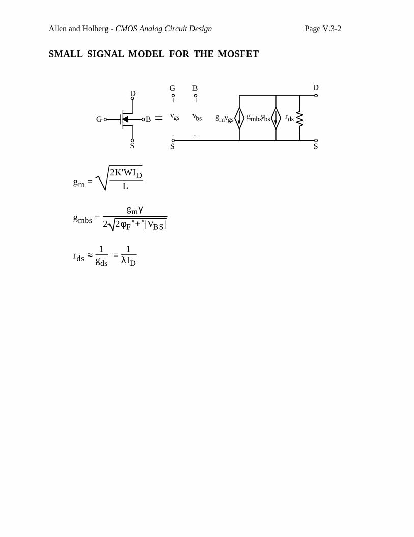
Allen and Holberg - CMOS Analog Circuit Design Page V.3-2
SMALL SIGNAL MODEL FOR THE MOSFET
rdsgmbsvbsgmvgs
+
-
vgs
+
-
vbs
G B D
SS
G B
S
D
gm = 2K'WID
L
gmbs = gmγ
2 2φF + |VBS|
rds ≈ 1
gds =
1λID
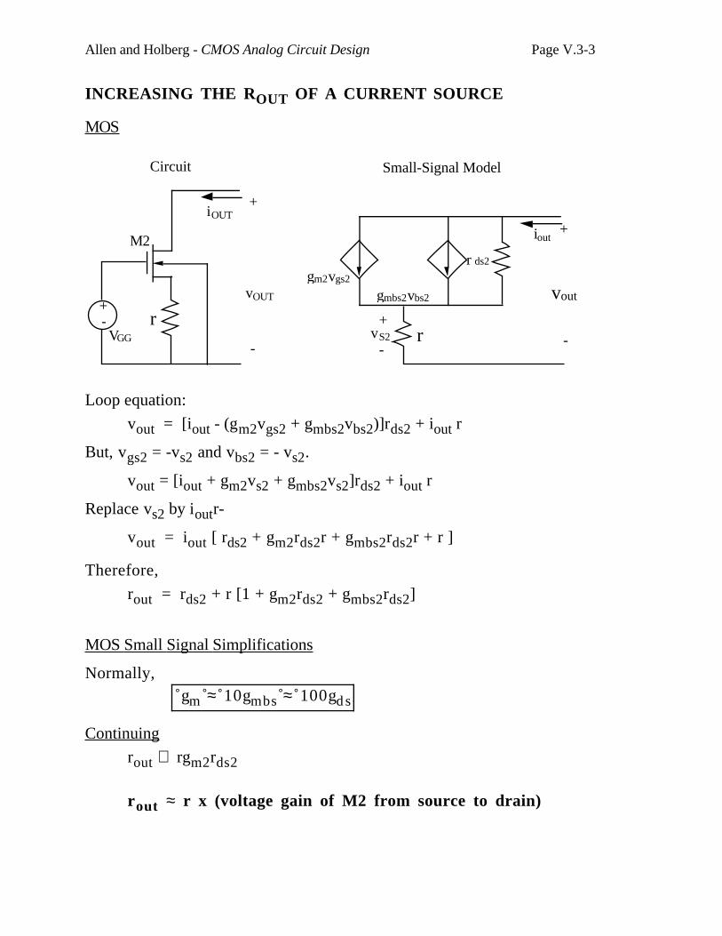
Allen and Holberg - CMOS Analog Circuit Design Page V.3-3
INCREASING THE ROUT OF A CURRENT SOURCE
MOS
VGG
r
+
-
M2
Circuit
vout
r ds2
+
-+
-
Small-Signal Model
r
vOUT
iOUT
vS2
+-
iout
gmbs2vbs2
gm2vgs2
Loop equation:
vout = [iout - (gm2vgs2 + gmbs2vbs2)]rds2 + iout r
But, vgs2 = -vs2 and vbs2 = - vs2.
vout = [iout + gm2vs2 + gmbs2vs2]rds2 + iout r
Replace vs2 by ioutr-
vout = iout [ rds2 + gm2rds2r + gmbs2rds2r + r ]
Therefore,
rout = rds2 + r [1 + gm2rds2 + gmbs2rds2]
MOS Small Signal Simplifications
Normally, gm ≈ 10gmbs ≈ 100gd s
Continuing
rout ≅ rgm2rds2
rout ≈ r x (voltage gain of M2 from source to drain)
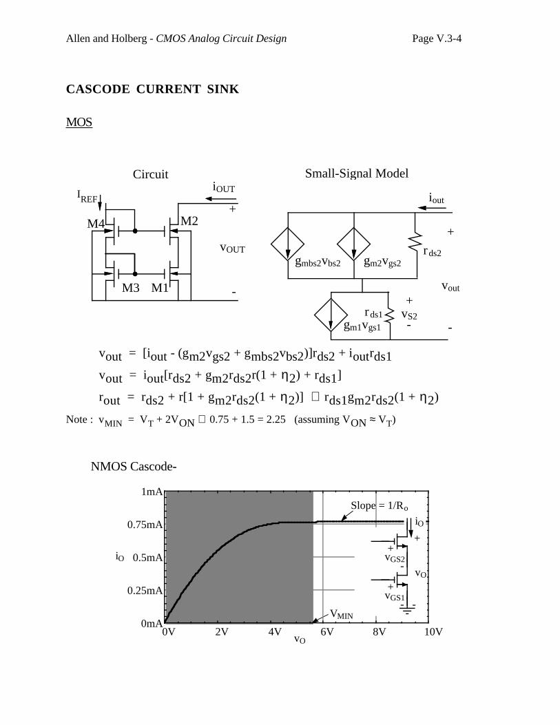
Allen and Holberg - CMOS Analog Circuit Design Page V.3-4
CASCODE CURRENT SINK
MOS
gmbs2vbs2 gm2vgs2rds2
iout
vout
+
-gm1vgs1
+
-
Small-Signal Model
vS2rds1
M4 M2
M3 M1
Circuit
+
-
vOUT
iOUTREFI
vout = [iout - (gm2vgs2 + gmbs2vbs2)]rds2 + ioutrds1
vout = iout[rds2 + gm2rds2r(1 + η2) + rds1]
rout = rds2 + r[1 + gm2rds2(1 + η2)] ≅ rds1gm2rds2(1 + η2)
Note : vMIN = VT + 2VON ≅ 0.75 + 1.5 = 2.25 (assuming VON ≈ VT)
NMOS Cascode-
0V 2V 4V 6V 8V 10VvO
iO
Slope = 1/Ro
0mA
0.25mA
0.5mA
0.75mA
1mA
-
+
-
iO
+
vO
+
-vGS2
vGS1
VMIN
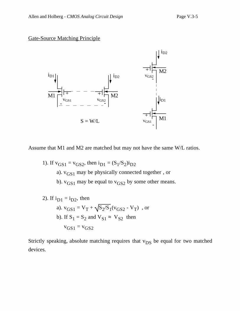
Allen and Holberg - CMOS Analog Circuit Design Page V.3-5
Gate-Source Matching Principle
S = W/L
+ +
- -M1 M2
iD1 iD2
vGS2vGS1
M1
+
-M2
iD2
vGS2
+
-
iD1
vGS1
Assume that M1 and M2 are matched but may not have the same W/L ratios.
1). If vGS1 = vGS2, then iD1 = (S1/S2)iD2
a). vGS1 may be physically connected together , or
b). vGS1 may be equal to vGS2 by some other means.
2). If iD1 = iD2, then
a). vGS1 = VT + S2/S1(vGS2 - VT) , or
b). If S1 = S2 and VS1 ≈ VS2 then
vGS1 = vGS2
Strictly speaking, absolute matching requires that vDS be equal for two matched
devices.
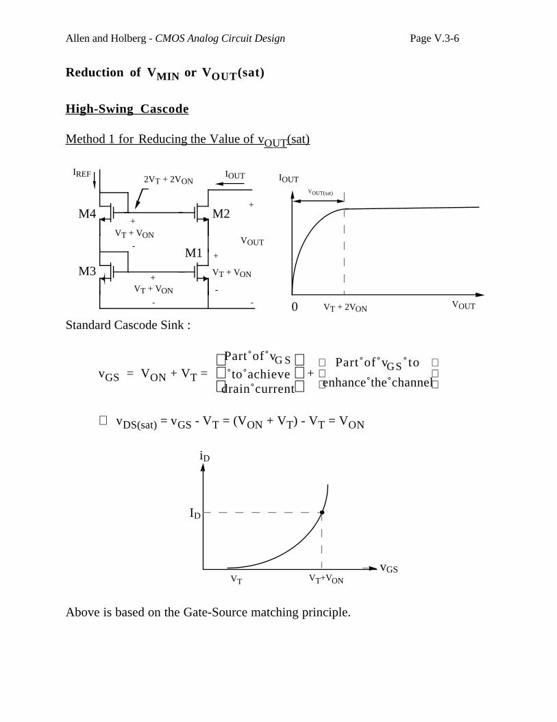
Allen and Holberg - CMOS Analog Circuit Design Page V.3-6
Reduction of VMIN or VOUT(sat)
High-Swing Cascode
Method 1 for Reducing the Value of v OUT (sat)
0
IOUTVOUT(sat)
VOUTVT + 2VON
M4 M2
M1
M3
IREF
+
-
+
-
IOUT
+
-
VOUT
+
-
VT + VON
VT + VON
2VT + 2VON
VT + VON
Standard Cascode Sink :
vGS = VON + VT =
Part of vG S
to achievedrain current
+
Part of vGS to
enhance the channel
∴ vDS(sat) = vGS - VT = (VON + VT) - VT = VON
iD
ID
vGSVT+VONVT
Above is based on the Gate-Source matching principle.
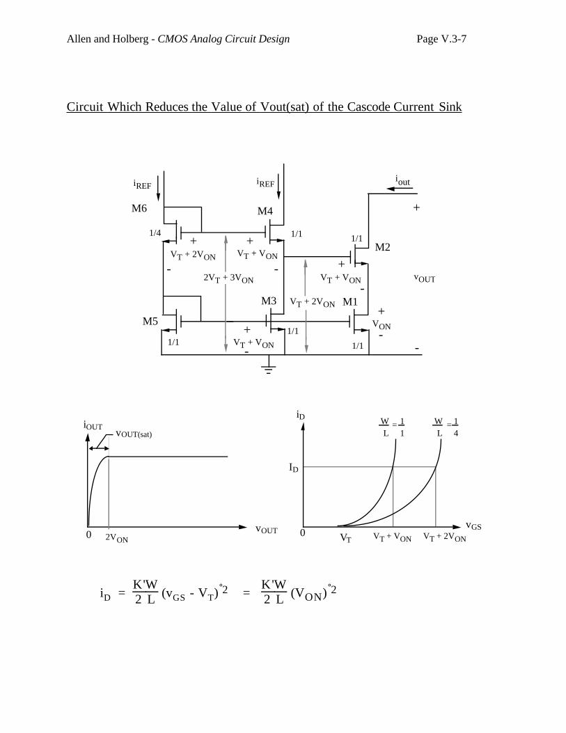
Allen and Holberg - CMOS Analog Circuit Design Page V.3-7
Circuit Whic h Reduces the Value of Vout(sat) of the Cascode Current Sink
M2
M6
+
-
+
-
M1
M5+
-
+
-
M4
VT + VON
VT + VON
VON
VT + 2VON
1/1
1/11/4
1/1
1/1
M3
ioutiREFiREF
+
-
vOUT2VT + 3VON
VT + VON
+
-
VT + 2VON
1/1
VT
vGS
iD
ID
WL
= 11
WL
= 14vOUT(sat)
vOUT
iOUT
0 02VON VT + VON VT + 2VON
iD = K'2
WL (vGS - VT) 2 =
K'2
WL (VON) 2
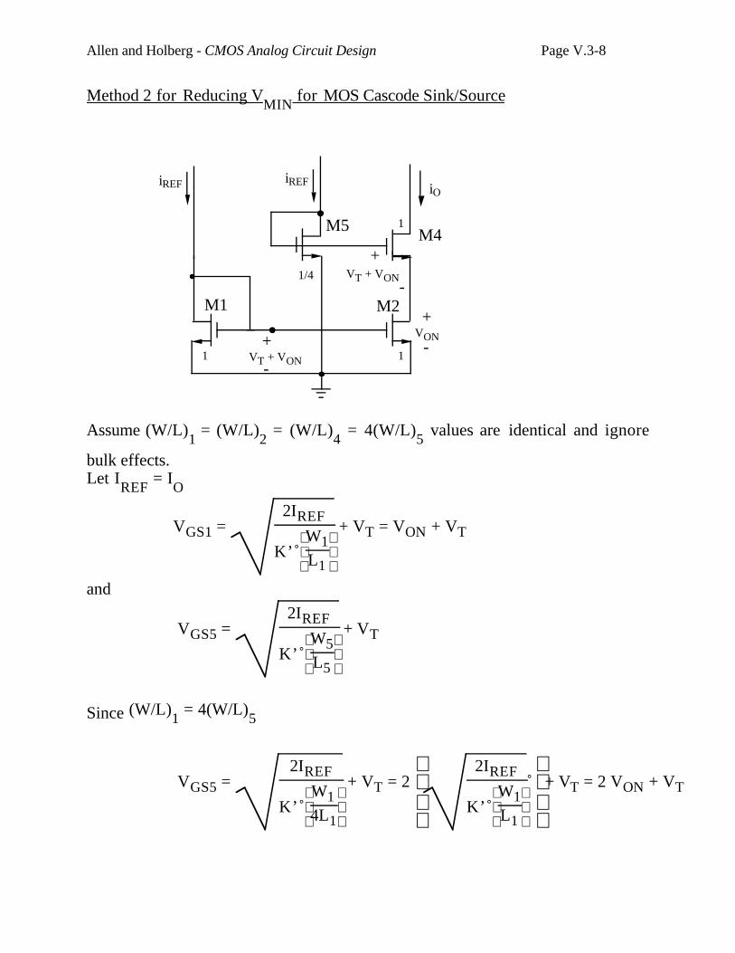
Allen and Holberg - CMOS Analog Circuit Design Page V.3-8
Method 2 for Reducing VMIN
for MOS Cascode Sink/Source
M4
+
-
M2M1+
-
+
-
iREF iO
M5
iREF
VT + VON
VT + VON
VON
1
1/4
1
1
Assume (W/L)1
= (W/L)2
= (W/L)4 = 4(W/L)
5 values are identical and ignore
bulk effects.Let I
REF = I
O
VGS1 = 2IREF
K’
W1
L1
+ VT = VON + VT
and
VGS5 = 2IREF
K’
W5
L5
+ VT
Since (W/L)1 = 4(W/L)
5
VGS5 = 2IREF
K’
W1
4L1
+ VT = 2
2IREF
K’
W1
L1
+ VT = 2 VON + VT
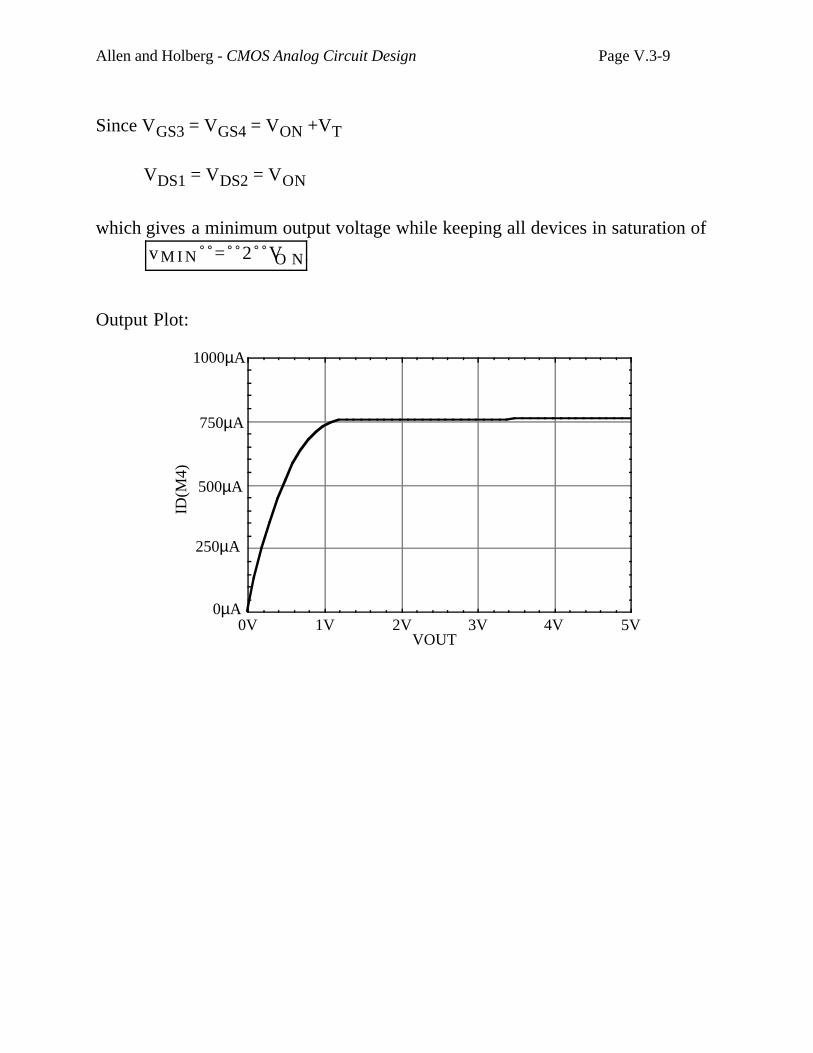
Allen and Holberg - CMOS Analog Circuit Design Page V.3-9
Since VGS3 = VGS4 = VON +VT
VDS1 = VDS2 = VON
which gives a minimum output voltage while keeping all devices in saturation ofv M I N = 2 VO N
Output Plot:
0V 1V 2V 3V 4V 5V
1000µA
750µA
500µA
250µA
0µA
ID(M
4)
VOUT
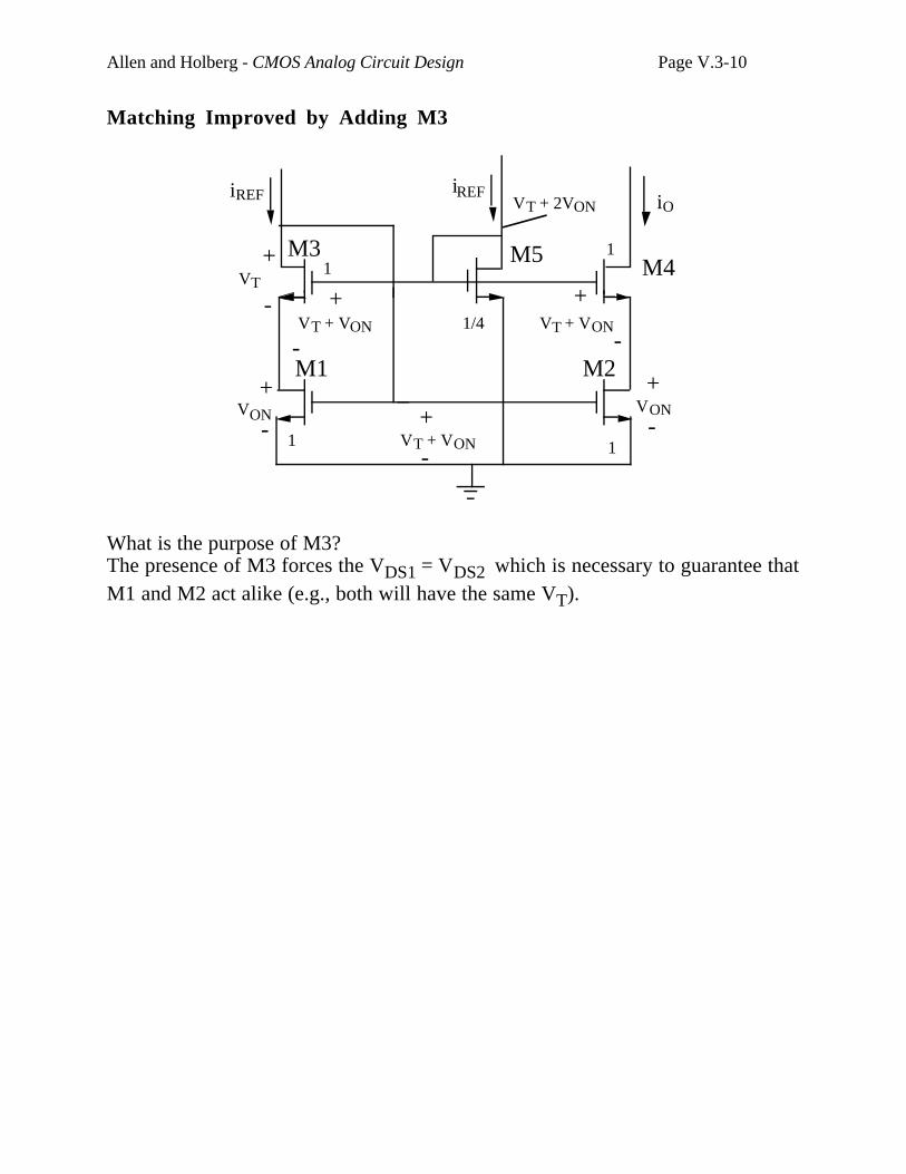
Allen and Holberg - CMOS Analog Circuit Design Page V.3-10
Matching Improved by Adding M3
M4M3
+
-
+
-M2M1
+
-
+
-
+
-
+
-
iREF iO
M5
iREF
VT
VT + VON
VON
VT + VON
VON
VT + VON
1
1
1/4
1
1
VT + 2VON
What is the purpose of M3?The presence of M3 forces the VDS1 = VDS2 which is necessary to guarantee thatM1 and M2 act alike (e.g., both will have the same VT).
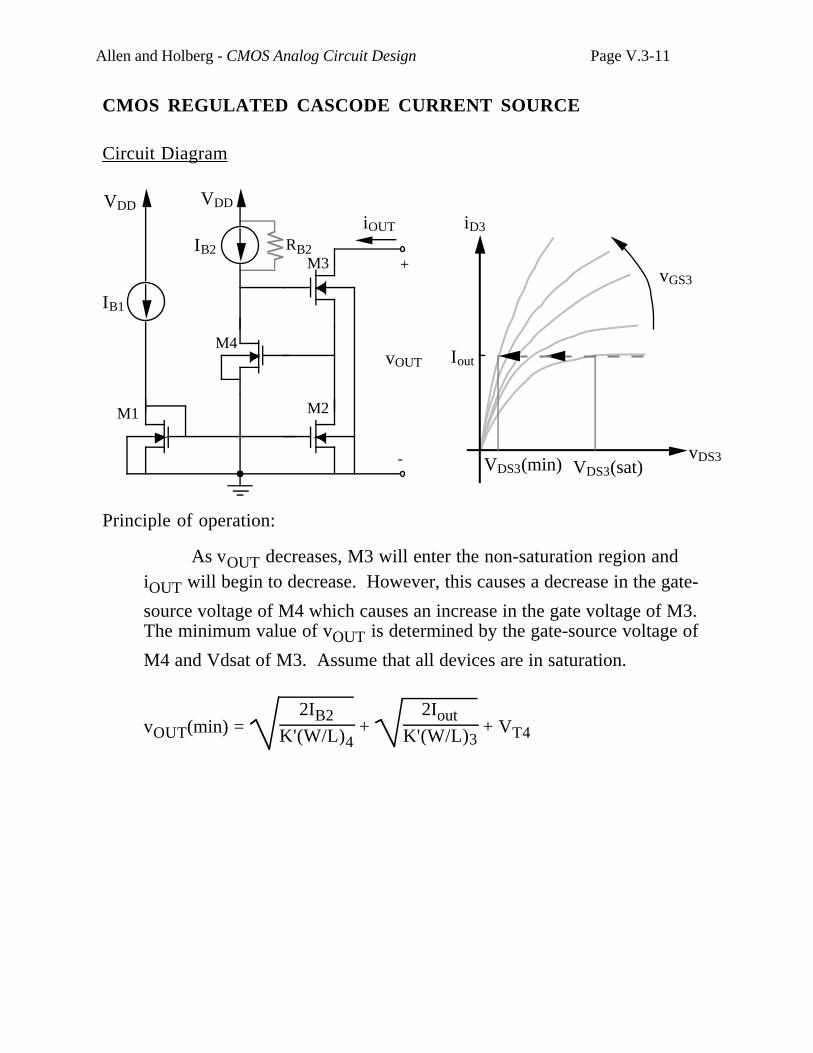
Allen and Holberg - CMOS Analog Circuit Design Page V.3-11
CMOS REGULATED CASCODE CURRENT SOURCE
Circuit Diagram
Iout
iD3
VDS3(min) VDS3(sat)vDS3
vGS3
VDDVDD
vOUT
iOUT
IB1
IB2
M1 M2
M4
M3 +
-
RB2
Principle of operation:
As vOUT decreases, M3 will enter the non-saturation region andiOUT will begin to decrease. However, this causes a decrease in the gate-
source voltage of M4 which causes an increase in the gate voltage of M3.The minimum value of vOUT is determined by the gate-source voltage of
M4 and Vdsat of M3. Assume that all devices are in saturation.
vOUT(min) = 2IB2
K'(W/L)4 +
2IoutK'(W/L)3
+ VT4
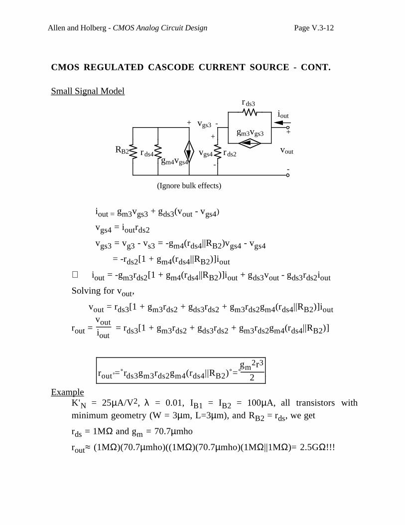
Allen and Holberg - CMOS Analog Circuit Design Page V.3-12
CMOS REGULATED CASCODE CURRENT SOURCE - CONT.
Small Signal Model
RB2
rds3
gm3vgs3
vgs3
rds2vgs4rds4gm4vgs4
+
-
vout
iout
(Ignore bulk effects)
+ -
+
-
iout = gm3vgs3 + gds3(vout - vgs4)
vgs4 = ioutrds2
vgs3 = vg3 - vs3 = -gm4(rds4||RB2)vgs4 - vgs4
= -rds2[1 + gm4(rds4||RB2)]iout
∴ iout = -gm3rds2[1 + gm4(rds4||RB2)]iout + gds3vout - gds3rds2iout
Solving for vout,
vout = rds3[1 + gm3rds2 + gds3rds2 + gm3rds2gm4(rds4||RB2)]iout
rout = voutiout
= rds3[1 + gm3rds2 + gds3rds2 + gm3rds2gm4(rds4||RB2)]
rout = rds3gm3rds2gm4(rds4||RB2) = gm
2r3
2
ExampleK'N = 25µA/V2, λ = 0.01, IB1 = IB2 = 100µA, all transistors withminimum geometry (W = 3µm, L=3µm), and RB2 = rds, we get
rds = 1MΩ and gm = 70.7µmho
rout≈ (1MΩ)(70.7µmho)((1MΩ)(70.7µmho)(1MΩ||1MΩ)= 2.5GΩ!!!
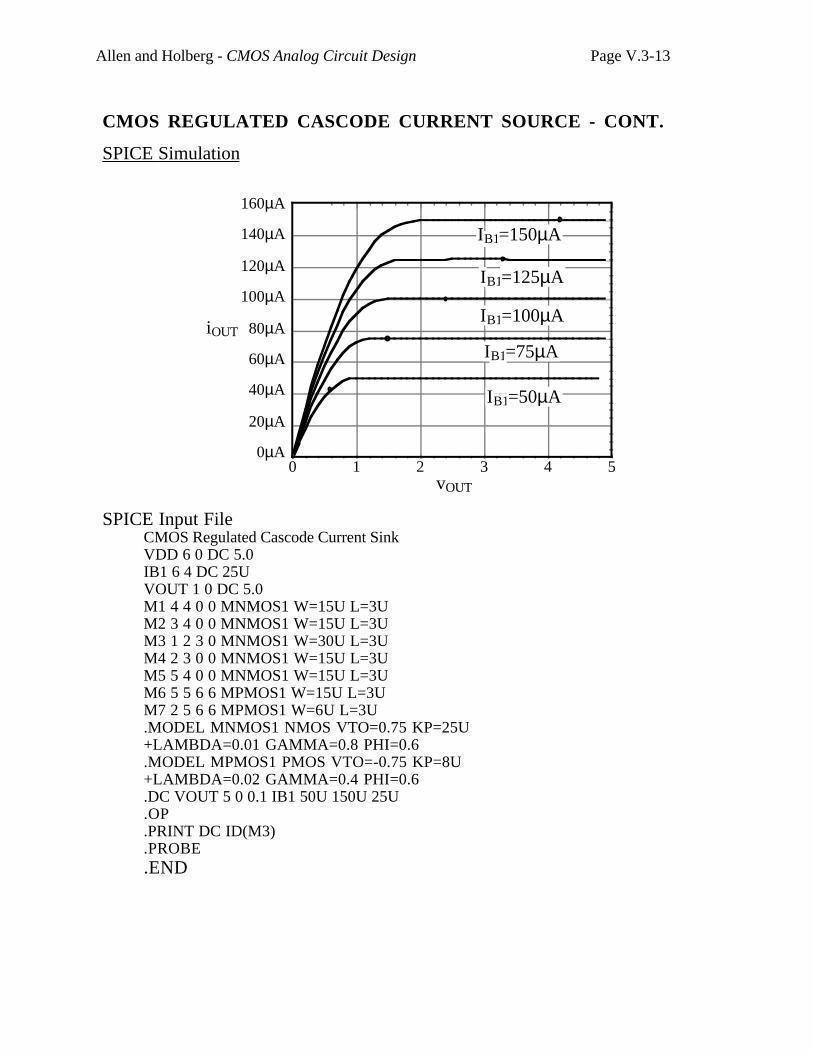
Allen and Holberg - CMOS Analog Circuit Design Page V.3-13
CMOS REGULATED CASCODE CURRENT SOURCE - CONT.
SPICE Simulation
0 1 2 3 4 5
160µA
140µA
120µA
100µA
80µA
60µA
40µA
20µA
0µA
iOUT
vOUT
IB1=50µA
IB1=75µA
IB1=100µA
IB1=125µA
IB1=150µA
SPICE Input FileCMOS Regulated Cascode Current SinkVDD 6 0 DC 5.0IB1 6 4 DC 25UVOUT 1 0 DC 5.0M1 4 4 0 0 MNMOS1 W=15U L=3UM2 3 4 0 0 MNMOS1 W=15U L=3UM3 1 2 3 0 MNMOS1 W=30U L=3UM4 2 3 0 0 MNMOS1 W=15U L=3UM5 5 4 0 0 MNMOS1 W=15U L=3UM6 5 5 6 6 MPMOS1 W=15U L=3UM7 2 5 6 6 MPMOS1 W=6U L=3U.MODEL MNMOS1 NMOS VTO=0.75 KP=25U+LAMBDA=0.01 GAMMA=0.8 PHI=0.6.MODEL MPMOS1 PMOS VTO=-0.75 KP=8U+LAMBDA=0.02 GAMMA=0.4 PHI=0.6.DC VOUT 5 0 0.1 IB1 50U 150U 25U.OP.PRINT DC ID(M3).PROBE.END
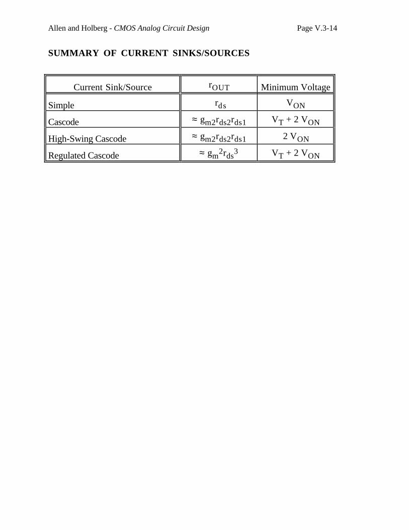
Allen and Holberg - CMOS Analog Circuit Design Page V.3-14
SUMMARY OF CURRENT SINKS/SOURCES
Current Sink/Source rOUT Minimum Voltage
Simple rds VON
Cascode ≈ gm2rds2rds1 VT + 2 VON
High-Swing Cascode ≈ gm2rds2rds1 2 VON
Regulated Cascode ≈ gm2rds
3 VT + 2 VON
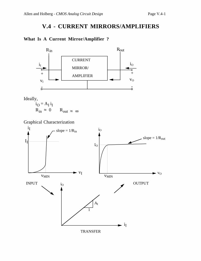
Allen and Holberg - CMOS Analog Circuit Design Page V.4-1
V.4 - CURRENT MIRRORS/AMPLIFIERS
What Is A Current Mirror/Amplifier ?
Rin
CURRENT
MIRROR/
AMPLIFIER+
-
Rout
+
-
iI iO
vOvI
Ideally,iO = AI iIRin ≈ 0 Rout ≈ ∞
Graphical Characterization
II
iI
vI
slope = 1/Rin
vMIN
slope = 1/Rout
vO
iO
vMIN
IO
INPUT
1
AI
iO
iI
OUTPUT
TRANSFER
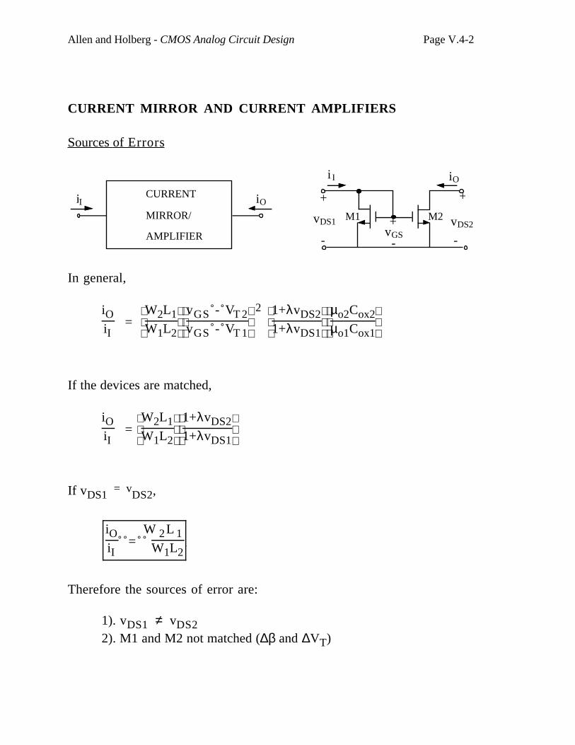
Allen and Holberg - CMOS Analog Circuit Design Page V.4-2
CURRENT MIRROR AND CURRENT AMPLIFIERS
Sources of Errors
CURRENT
MIRROR/
AMPLIFIER
iI iO
M1 M2+
-vGS
+
-
vDS2
+
-
vDS1
i I iO
In general,
iOiI
=
W2L1
W1L2
vGS - VT 2
vGS - VT 1 2
1+λvDS2
1+λvDS1
µo2Cox2
µo1Cox1
If the devices are matched,
iOiI
=
W2L1
W1L2
1+λvDS2
1+λvDS1
If vDS1 = v
DS2,
iOiI
= W 2L 1
W1L2
Therefore the sources of error are:
1). vDS1 ≠ vDS22). M1 and M2 not matched (∆β and ∆VT)
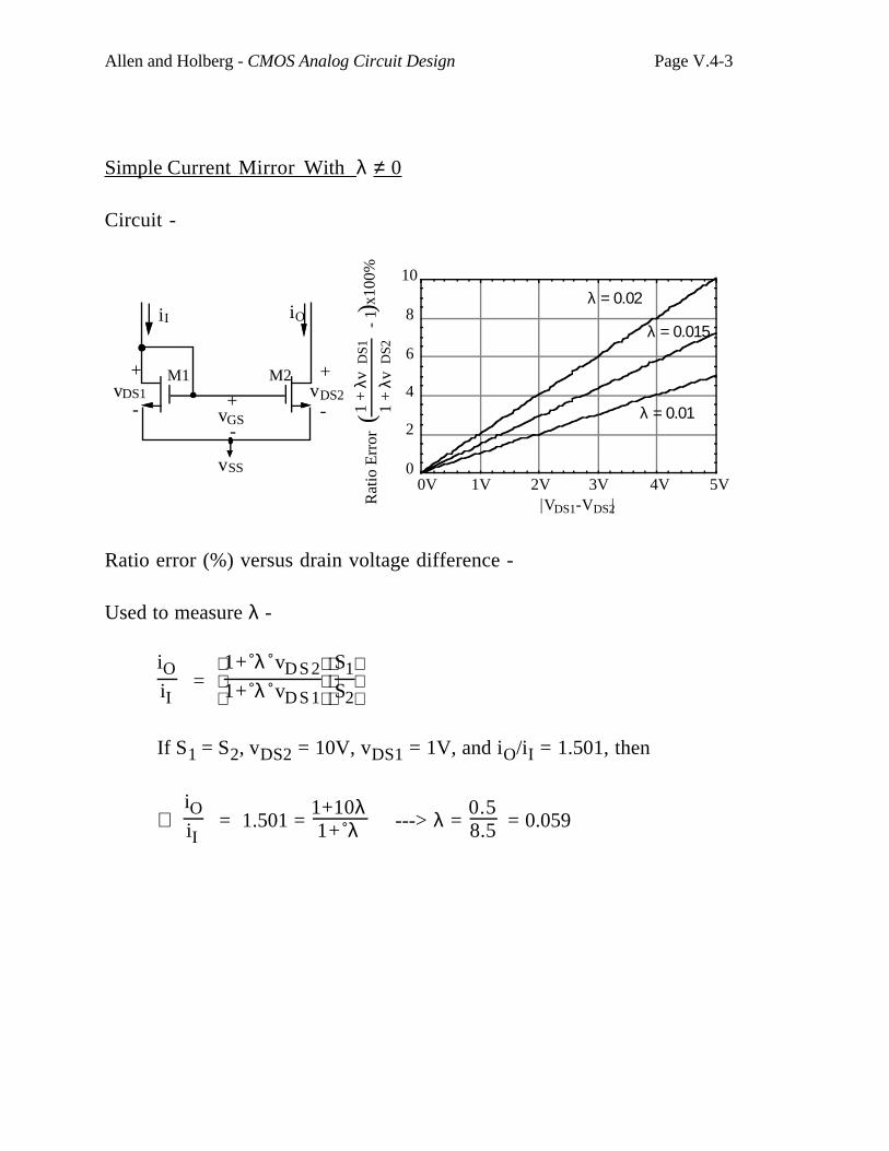
Allen and Holberg - CMOS Analog Circuit Design Page V.4-3
Simple Current Mirror With λ ≠ 0
Circuit -
M1 M2
iI iO
+ +
--vDS1 vDS2
vSS
+
-vGS
0
2
4
6
8
10
0V 1V 2V 3V 4V 5V
Rat
io E
rror
1
+ λ
vD
S1
1 +
λv
DS2
(-
1) x10
0%
λ = 0.02
λ = 0.015
λ = 0.01
VDS1-VDS2
Ratio error (%) versus drain voltage difference -
Used to measure λ -
iOiI
=
1+ λ vDS2
1+ λ vDS1
S1
S2
If S1 = S2, vDS2 = 10V, vDS1 = 1V, and iO/iI = 1.501, then
∴ iOiI
= 1.501 = 1+10λ1+ λ ---> λ =
0.58.5 = 0.059
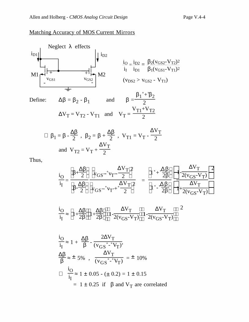
Allen and Holberg - CMOS Analog Circuit Design Page V.4-4
Matching Accuracy of MOS Current Mirrors
+
-
M1
iD1
vGS1
+
-M2
iD2
vGS2
iOiI
= iD2
iD1 = β2(vGS2-VT2)2
β1(vGS1-VT1)2
(vDS2 > vGS2 - VT1)
Neglect λ effects
Define: ∆β = β2 - β1 and β = β1 + β2
2
∆VT = VT2 - VT1 and VT = VT1+VT2
2
∴ β 1 = β - ∆β2 , β2 = β +
∆β2 , VT1 = VT -
∆VT2
and VT2 = VT + ∆VT
2
Thus,
iOiI
=
β+
∆β2
β-
∆β2
vGS - vT -∆VT
22
vGS - vT + ∆VT
22 =
1 + ∆β2β
1 - ∆ β2β
1-
∆VT2(vGS-VT)
1+∆VT
2(vGS-VT)
2
iOiI
≈
1+∆β2β
1+∆β2β
1-∆VT
2(vGS-VT)
1-∆VT
2(vGS-VT) 2
iOiI
≈ 1 + ∆ββ -
2∆VT(vGS - VT),
∆ββ ≈ ± 5% ,
∆VT(vGS - VT) = ± 10%
∴ iOiI
≈ 1 ± 0.05 - (± 0.2) = 1 ± 0.15
= 1 ± 0.25 if β and VT are correlated
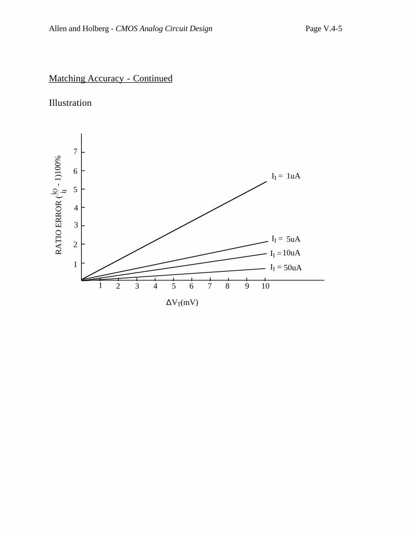
Allen and Holberg - CMOS Analog Circuit Design Page V.4-5
Matching Accuracy - Continued
Illustration
∆VT(mV)
1 2 3 4 5 6 7 98 10
RA
TIO
ER
RO
R (
i O i I -
1)1
00%
1
2
3
4
5
6
7
II = 1uA
II = 5uA
II =10uA
II = 50uA
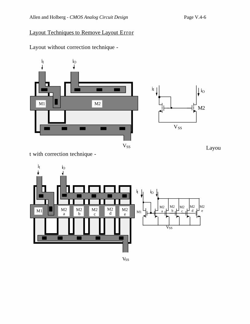
Allen and Holberg - CMOS Analog Circuit Design Page V.4-6
Layout Techniques to Remove Layout Error
Layout without correction technique -
iI iO
M1 M2
VSS
iI
M2
iO
VSS
Layout with correction technique -
M1
VSS
iI iO
M2 a
M2 b
M2 c
M2 d
M2 e
iI
M1
M2 e
iO
M2 a
M2 b
M2 c
M2 d
VSS

Allen and Holberg - CMOS Analog Circuit Design Page V.4-7
Practical Current Mirrors/Amplifiers
• Simple mirror• Cascode current mirror• Wilson current mirror
Simple Current Mirror -
00 1 2 3 4 5
20uA
40uA
60uA
vOUT
iOUT
iI = 60uA
iI = 50uA
iI = 40uA
iI = 30uA
iI = 20uA
iI = 10uA
Current mirrors and amplifiers.MODEL MNMOS1 NMOS VTO=0.75 KP=25U+LAMBDA=0.01 GAMMA=0.8 PHI=0.6M1 1 1 0 0 MNMOS1 W=3U L=3UM2 3 1 0 0 MNMOS1 W=3U L=3UIIN 0 1 VOUT 3 0 .DC VOUT 0 5 0.1 +IIN 0 60U 10U .PRINT DC ID(M2).PROBE.END
M1
iI
M2
iO
3u3u
3u3u +
-vO
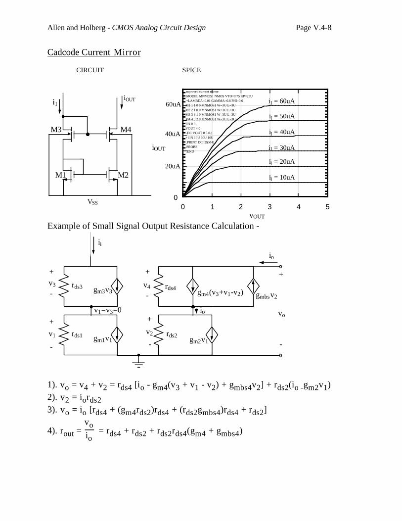
Allen and Holberg - CMOS Analog Circuit Design Page V.4-8
Cadcode Current Mirror
00 1 2 3 4 5
iOUT
60uA
40uA
20uA
vOUT
iI = 60uA
iI = 50uA
iI = 40uA
iI = 30uA
iI = 20uA
iI = 10uA
M4
M2M1
M3
iOUT
VSS
iI
CIRCUIT SPICE
mproved current mirror.MODEL MNMOS1 NMOS VTO=0.75 KP=25U+LAMBDA=0.01 GAMMA=0.8 PHI=0.6M1 1 1 0 0 MNMOS1 W=3U L=3UM2 2 1 0 0 MNMOS1 W=3U L=3UM3 3 3 1 0 MNMOS1 W=3U L=3UM4 4 3 2 0 MNMOS1 W=3U L=3UIIN 0 3 VOUT 4 0 .DC VOUT 0 5 0.1+ IIN 10U 60U 10U.PRINT DC ID(M4).PROBE.END
Example of Small Signal Output Resistance Calculation -
rds3
rds1 rds2
rds4
+
-
v1 v2
+
-
+
-v3
+
-v4
ii
gm3v3
gm1v1 gm2v1
gmbsv2gm4(v3+v1-v2)
io
+
-
vov1=v3=0 io
1). vo = v4 + v2 = rds4 [io - gm4(v3 + v1 - v2) + gmbs4v2] + rds2(io -gm2v1)2). v2 = iords23). vo = io [rds4 + (gm4rds2)rds4 + (rds2gmbs4)rds4 + rds2]
4). rout = voio
= rds4 + rds2 + rds2rds4(gm4 + gmbs4)
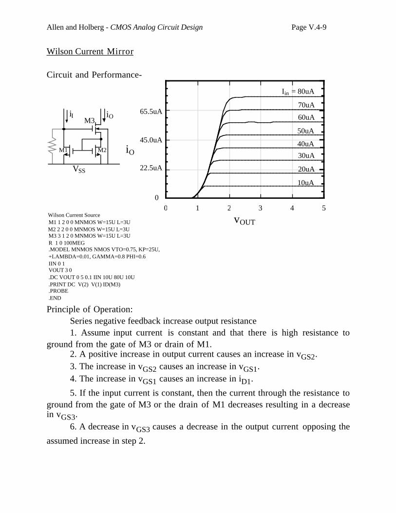
Allen and Holberg - CMOS Analog Circuit Design Page V.4-9
Wilson Current Mirror
Circuit and Performance-
iOiI
M1 M2
M3
VSS
0 1 2 3 4 50
22.5uA
45.0uA
65.5uA
iO
vOUTWilson Current SourceM1 1 2 0 0 MNMOS W=15U L=3UM2 2 2 0 0 MNMOS W=15U L=3UM3 3 1 2 0 MNMOS W=15U L=3UR 1 0 100MEG.MODEL MNMOS NMOS VTO=0.75, KP=25U, +LAMBDA=0.01, GAMMA=0.8 PHI=0.6IIN 0 1 VOUT 3 0 .DC VOUT 0 5 0.1 IIN 10U 80U 10U.PRINT DC V(2) V(1) ID(M3).PROBE.END
Iin = 80uA
70uA
60uA
50uA
40uA
30uA
20uA
10uA
Principle of Operation:Series negative feedback increase output resistance1. Assume input current is constant and that there is high resistance to
ground from the gate of M3 or drain of M1.2. A positive increase in output current causes an increase in vGS2.3. The increase in vGS2 causes an increase in vGS1.4. The increase in vGS1 causes an increase in iD1.
5. If the input current is constant, then the current through the resistance toground from the gate of M3 or the drain of M1 decreases resulting in a decreasein vGS3.
6. A decrease in vGS3 causes a decrease in the output current opposing the
assumed increase in step 2.
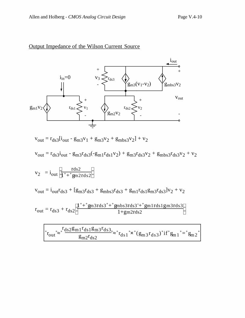
Allen and Holberg - CMOS Analog Circuit Design Page V.4-10
Output Impedance of the Wilson Current Source
rds1
-
+
v1 rds2 v2
+
-
+
-
+
-
iin=0
gm1v2gm2v2
gmbs3v2gm3(v1-v2)v3 rds3
iout
vout
vout = rds3[iout - gm3v1 + gm3v2 + gmbs3v2] + v2
vout = rds3iout - gm3rds3(-gm1rds1v2) + gm3rds3v2 + gmbs3rds3v2 + v2
v2 = iout
rds2
1 + gm2rds2
vout = ioutrds3 + [gm3rds3 + gmbs3rds3 + gm1rds1gm3rds3]v2 + v2
rout = rds3 + rds2
1 + gm3rds3 + gmbs3rds3 + gm1rds1gm3rds3
1+gm2rds2
rout ≈ rds2gm1rds1gm3rds3
gm2rds2 ≈ rds1 × (gm 3 rds3) if gm 1 = gm 2
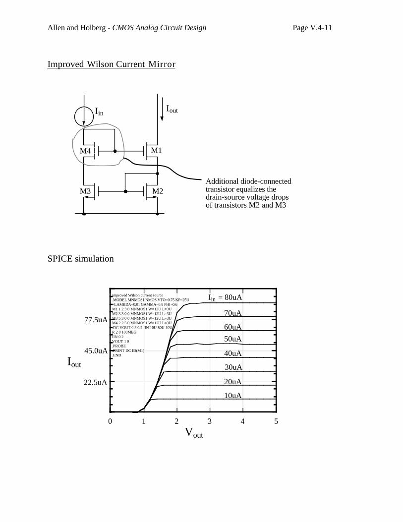
Allen and Holberg - CMOS Analog Circuit Design Page V.4-11
Improved Wilson Current Mirror
IoutIin
M4
M3 M2
M1
Additional diode-connectedtransistor equalizes the drain-source voltage dropsof transistors M2 and M3
SPICE simulation
0 1 2 3 4 5
22.5uA
45.0uA
77.5uA
Iin = 80uA
70uA
60uA
50uA
40uA
30uA
20uA
10uA
Iout
Vout
improved Wilson current source.MODEL MNMOS1 NMOS VTO=0.75 KP=25U+LAMBDA=0.01 GAMMA=0.8 PHI=0.6M1 1 2 3 0 MNMOS1 W=12U L=3UM2 3 3 0 0 MNMOS1 W=12U L=3UM3 5 3 0 0 MNMOS1 W=12U L=3UM4 2 2 5 0 MNMOS1 W=12U L=3U.DC VOUT 0 5 0.2 IIN 10U 80U 10UR 2 0 100MEGIIN 0 2 VOUT 1 0.PROBE.PRINT DC ID(M1).END
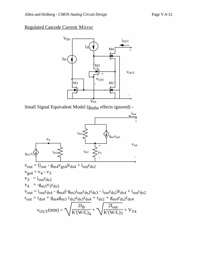
Allen and Holberg - CMOS Analog Circuit Design Page V.4-12
Regulated Cascode Current Mirror
vOUT
iOUT
M1 M2
M4
M3
+
-
+
-vGS4
IIN
IB
VSS
VDD
Small Signal Equivalent Model (gmbs effects ignored) -
rds2
--
+
v3rds3
+
iout
vout
gm3v3
v4gm4vgs4
rds4
vout = (iout - gm4vgs4)rds4 + ioutrds2vgs4 = v4 - v3v3 = ioutrds2v4 = -gm3v3rds3vout = ioutrds4 - gm4(-gm3ioutrds2rds3 - ioutrds2)rds4 + ioutrds2rout = rds4 + gm4gm3 rds2rds3rds4 + rds2 + gm4rds2rds4
vOUT(min) = 2IB
K'(W/L)4 +
2IoutK'(W/L)3
+ VT4
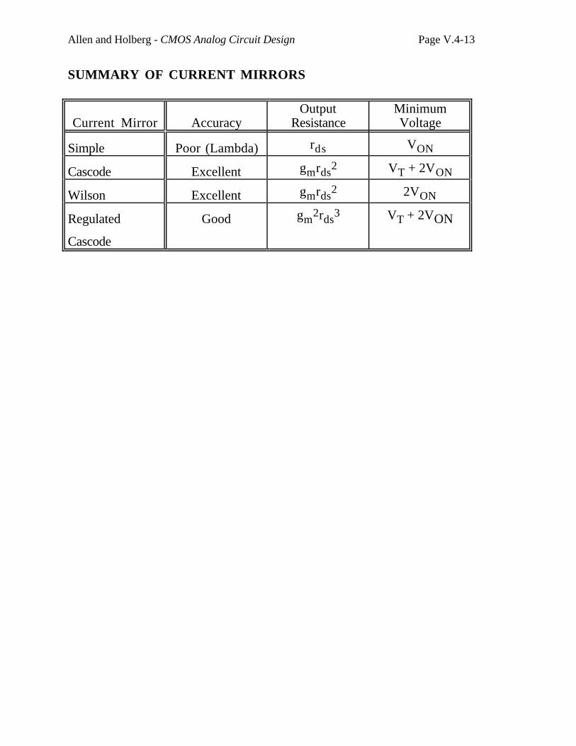
Allen and Holberg - CMOS Analog Circuit Design Page V.4-13
SUMMARY OF CURRENT MIRRORS
Current Mirror AccuracyOutput
ResistanceMinimumVoltage
Simple Poor (Lambda) rds VON
Cascode Excellent gmrds2 VT + 2VON
Wilson Excellent gmrds2 2VON
Regulated
Cascode
Good gm2rds
3 VT + 2VON
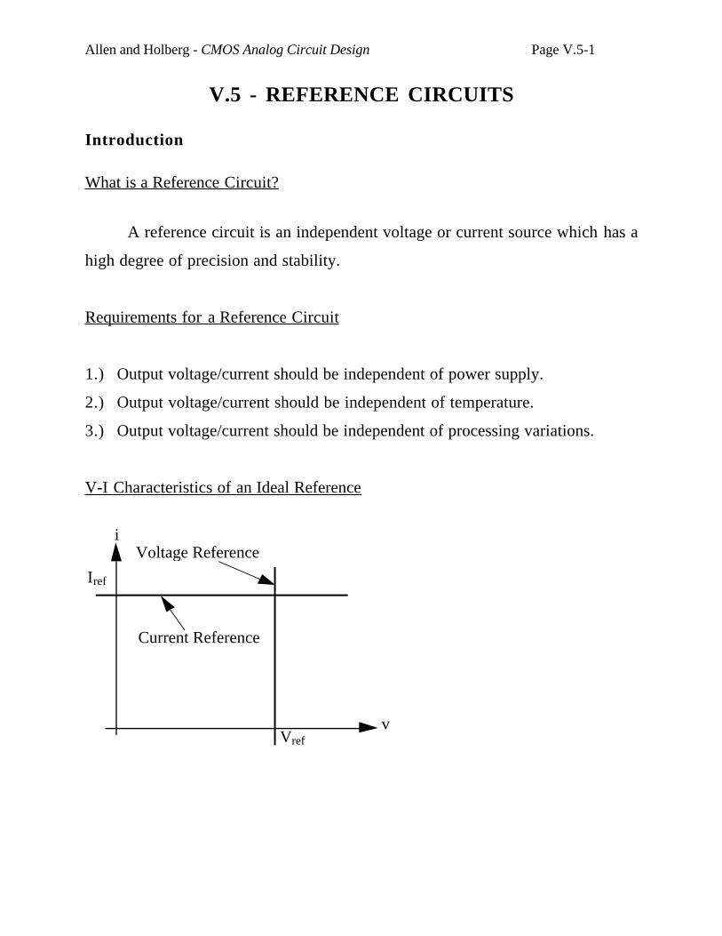
Allen and Holberg - CMOS Analog Circuit Design Page V.5-1
V.5 - REFERENCE CIRCUITS
Introduction
What is a Reference Circuit?
A reference circuit is an independent voltage or current source which has a
high degree of precision and stability.
Requirements for a Reference Circuit
1.) Output voltage/current should be independent of power supply.
2.) Output voltage/current should be independent of temperature.
3.) Output voltage/current should be independent of processing variations.
V-I Characteristics of an Ideal Reference
Iref
Vref
i
v
Voltage Reference
Current Reference
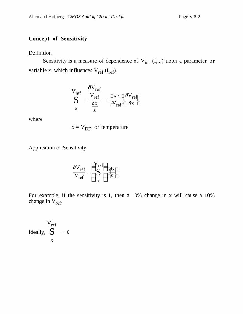
Allen and Holberg - CMOS Analog Circuit Design Page V.5-2
Concept of Sensitivity
Definition
Sensitivity is a measure of dependence of Vref (Iref) upon a parameter or
variable x which influences Vref (Iref).
Vref
Sx
=
∂VrefVref∂xx
=
x
Vref
∂Vref
∂x
where
x = VDD or temperature
Application of Sensitivity
∂VrefVref
=
Vref
Sx
∂x
x
For example, if the sensitivity is 1, then a 10% change in x will cause a 10%change in Vref.
Ideally,
Vref
Sx
→ 0
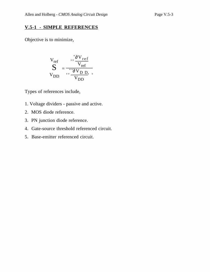
Allen and Holberg - CMOS Analog Circuit Design Page V.5-3
V.5-1 - SIMPLE REFERENCES
Objective is to minimize,
Vref
SVDD
=
∂V r e f
Vref
∂V D D
VDD
Types of references include,
1. Voltage dividers - passive and active.
2. MOS diode reference.
3. PN junction diode reference.
4. Gate-source threshold referenced circuit.
5. Base-emitter referenced circuit.
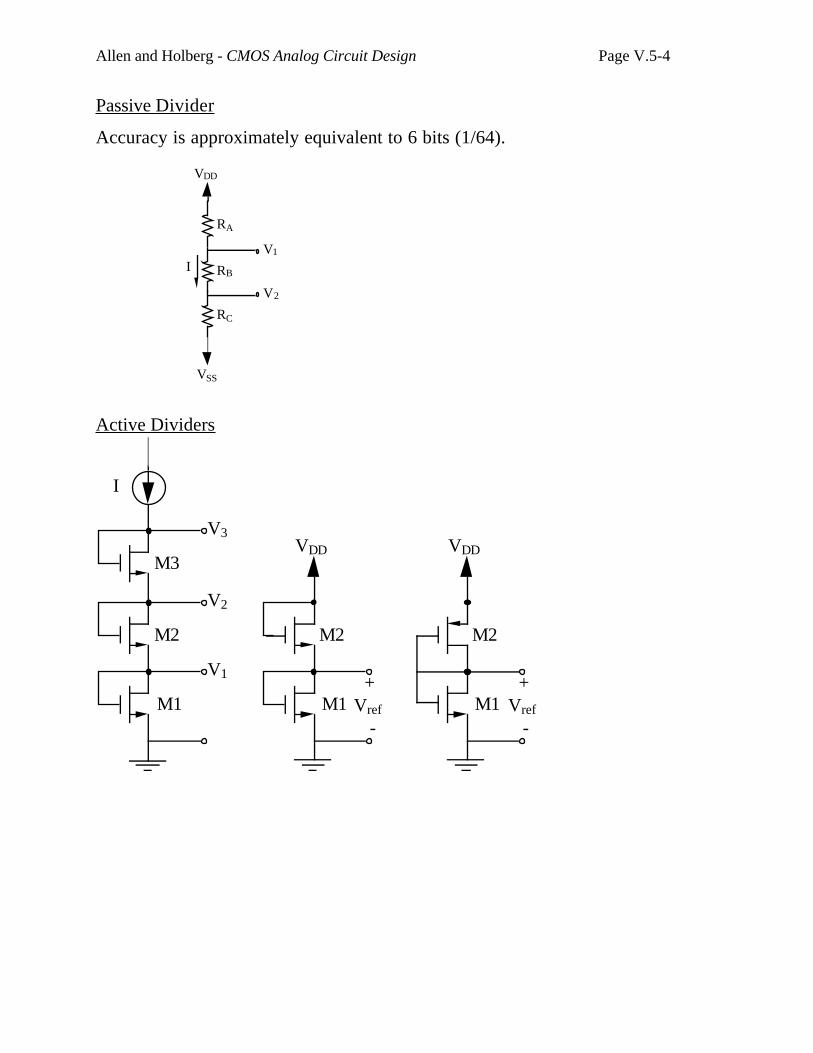
Allen and Holberg - CMOS Analog Circuit Design Page V.5-4
Passive Divider
Accuracy is approximately equivalent to 6 bits (1/64).
Active Dividers
I
V2
V1
V3
M3
M2
M1
M2
M1+
-Vref
VDD
M2
M1+
-Vref
VDD
I
RA
RB
VDD
VSS
RC
V1
V2
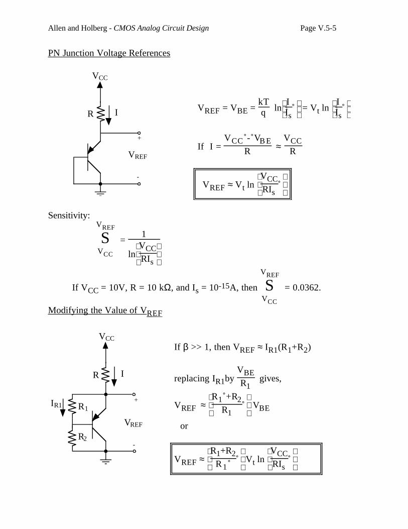
Allen and Holberg - CMOS Analog Circuit Design Page V.5-5
PN Ju nction Voltage References
R I
VCC
VREF
+
-
Sensitivity:VREF
SVCC
= 1
ln
VCC
RIs
If VCC = 10V, R = 10 kΩ, and Is = 10-15A, then
VREF
SVCC
= 0.0362.
Modifying the Value of V REF
If β >> 1, then VREF ≈ IR1(R1+R2)
replacing IR1by VBER1
gives,
VREF ≈
R1 +R2
R1 VBE
or
VREF ≈
R1+R2
R1 Vt ln
VCC
RIs
VREF = VBE = kTq ln
I
Is = Vt ln
I
Is
If I = VCC - VB E
R ≈ VCC
R
VREF ≈ Vt ln
VCC
RIs
R I
VCC
VREF
+
-
R1
R2
IR1
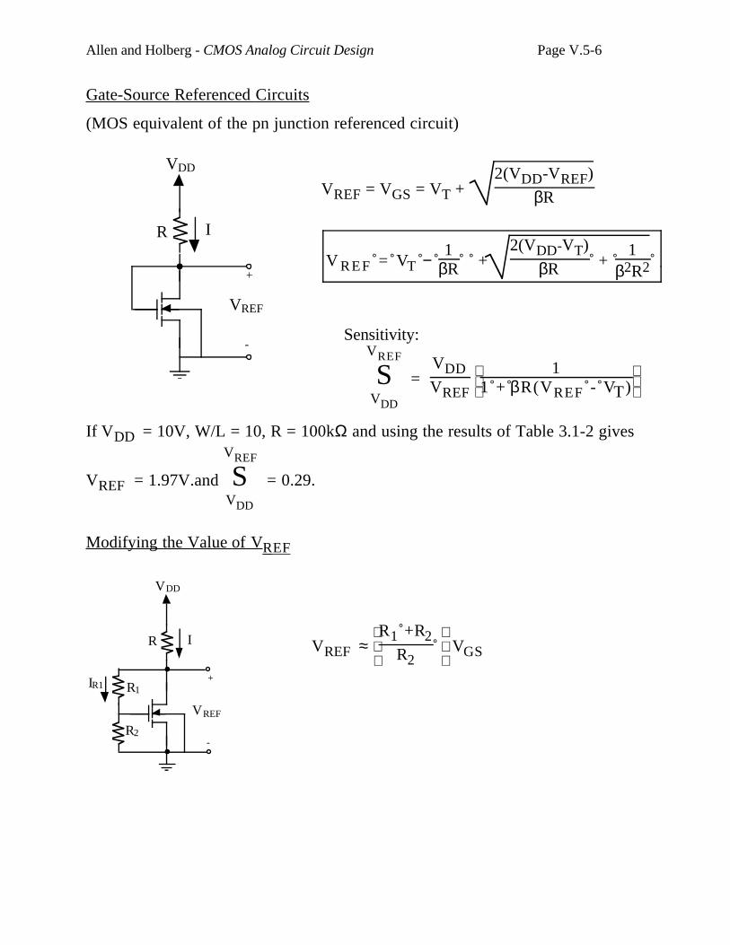
Allen and Holberg - CMOS Analog Circuit Design Page V.5-6
Gate-Source Referenced Circuits
(MOS equivalent of the pn junction referenced circuit)
R I
VREF
+
-
VDD
If VDD = 10V, W/L = 10, R = 100kΩ and using the results of Table 3.1-2 gives
VREF = 1.97V.and
VREF
SVDD
= 0.29.
Modifying the Value of V REF
VREF ≈
R1 +R2
R2 VGS
VREF = VGS = VT + 2(VDD-VREF)
βR
V REF = VT − 1
βR +2(VDD-VT)
βR + 1
β2R2
Sensitivity:
VREF
SVDD
= VDDVREF
1
1 + βR(VREF - VT)
R I
VREF
+
-
R1
R2
IR1
VDD
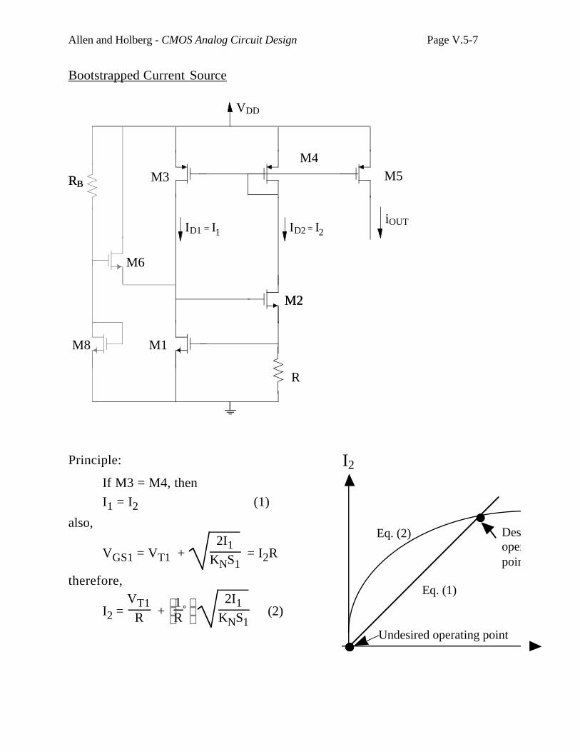
Allen and Holberg - CMOS Analog Circuit Design Page V.5-7
Bootstrapped Current Source
M5
ID2
M2
R
ID1
M6
RB
iOUT
M2
M3
VDD
RB
I1 = I2=
M4
M1M8
Principle:
If M3 = M4, then
I1 = I2 (1)
also,
VGS1 = VT1 + 2I1
KNS1 = I2R
therefore,
I2 = VT1
R +
1
R 2I1
KNS1 (2)
I2
Eq. (2)
Eq. (1)
Desiredoperatingpoint
Undesired operating point
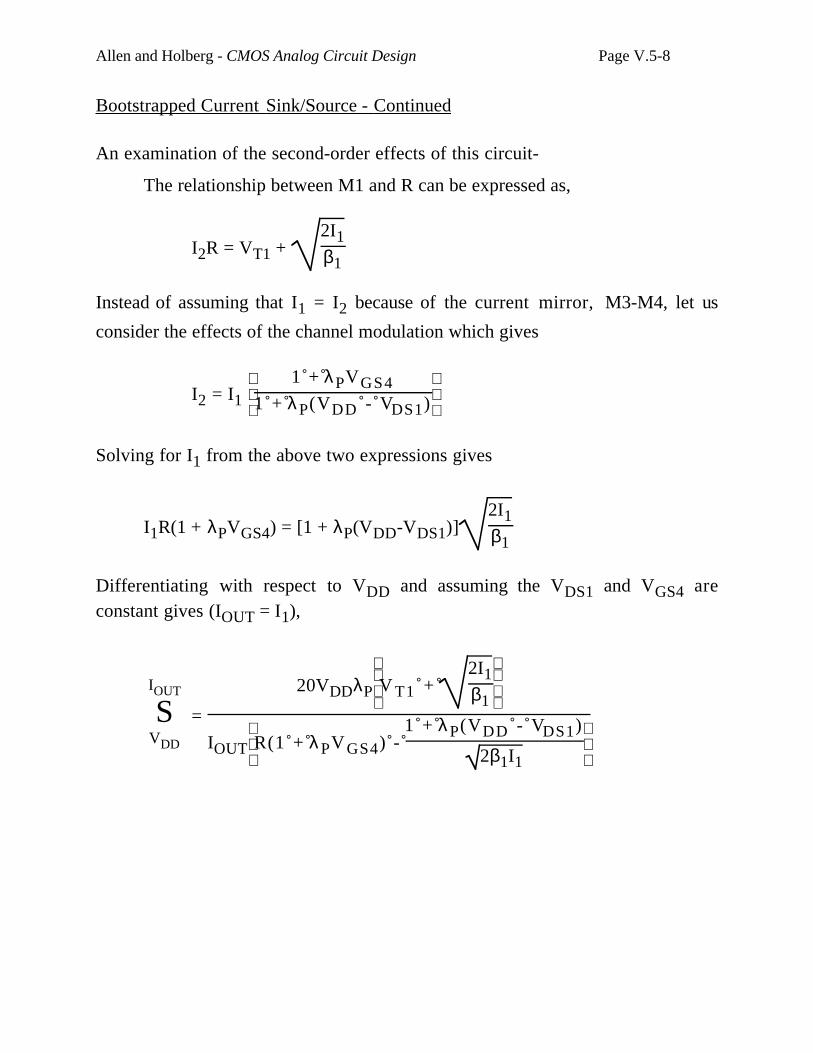
Allen and Holberg - CMOS Analog Circuit Design Page V.5-8
Bootstrapped Current Sink/Source - Continued
An examination of the second-order effects of this circuit-
The relationship between M1 and R can be expressed as,
I2R = VT1 + 2I1β1
Instead of assuming that I1 = I2 because of the current mirror, M3-M4, let us
consider the effects of the channel modulation which gives
I2 = I1
1 + λPVGS4
1 + λ P(VDD - VDS1)
Solving for I1 from the above two expressions gives
I1R(1 + λPVGS4) = [1 + λP(VDD-VDS1)]2I1β1
Differentiating with respect to VDD and assuming the VDS1 and VGS4 areconstant gives (IOUT = I1),
IOUT
SVDD
=
20VDDλP
V T1 + 2I1β1
IOUT
R(1 + λ PVGS4) - 1 + λ P(VDD - VDS1)
2β1I1
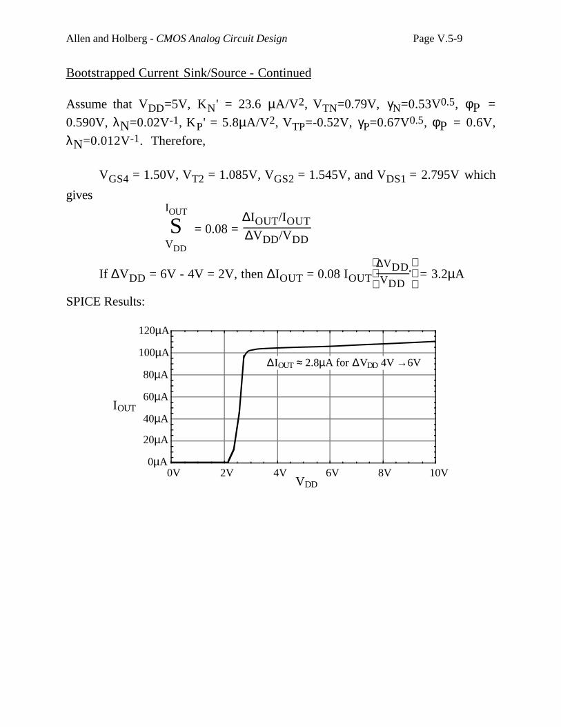
Allen and Holberg - CMOS Analog Circuit Design Page V.5-9
Bootstrapped Current Sink/Source - Continued
Assume that VDD=5V, KN' = 23.6 µA/V2, VTN=0.79V, γN=0.53V0.5, φP =
0.590V, λN=0.02V-1, KP' = 5.8µA/V2, VTP=-0.52V, γP=0.67V0.5, φP = 0.6V,
λN=0.012V-1. Therefore,
VGS4 = 1.50V, VT2 = 1.085V, VGS2 = 1.545V, and VDS1 = 2.795V which
gives
IOUT
SVDD
= 0.08 = ∆IOUT/IOUT∆VDD/VDD
If ∆VDD = 6V - 4V = 2V, then ∆IOUT = 0.08 IOUT
∆VDD
VDD = 3.2µA
SPICE Results:
0V 2V 4V 6V 8V 10V
120µA
100µA
80µA
60µA
40µA
20µA
0µA
VDD
IOUT
∆IOUT ≈ 2.8µA for ∆VDD 4V →6V
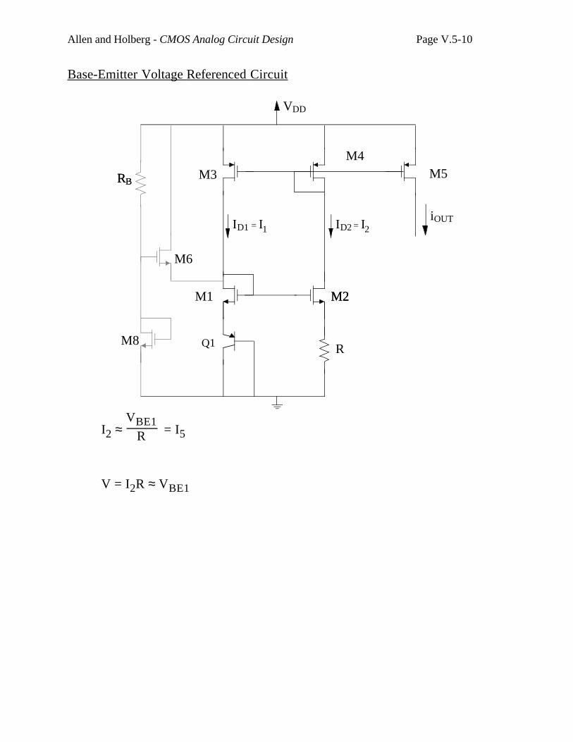
Allen and Holberg - CMOS Analog Circuit Design Page V.5-10
Base-Emitter Voltage Referenced Circuit
M5
ID2
M2
R
ID1
M6
RB
iOUT
M2
M3
VDD
RB
I1 = I2=
M4
M1
M8 Q1
I2 ≈ VBE1
R = I5
V = I2R ≈ VBE1
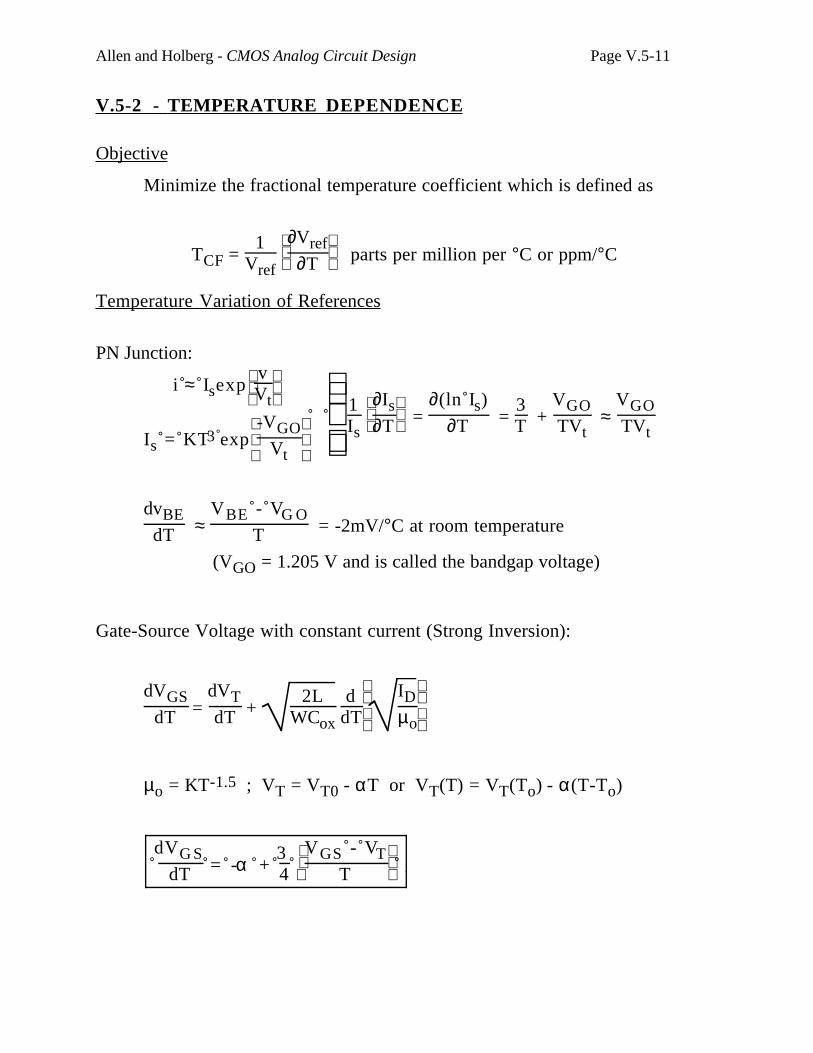
Allen and Holberg - CMOS Analog Circuit Design Page V.5-11
V.5-2 - TEMPERATURE DEPENDENCE
Objective
Minimize the fractional temperature coefficient which is defined as
TCF = 1
Vref
∂Vref
∂T parts per million per °C or ppm/°C
Temperature Variation of References
PN Junction:
i ≈ Isexp
v
Vt
Is = KT3 exp
-VGO
Vt
1Is
∂Is
∂T = ∂(ln Is)
∂T = 3T +
VGOTVt
≈ VGOTVt
dvBEdT ≈
VBE - VG OT = -2mV/°C at room temperature
(VGO = 1.205 V and is called the bandgap voltage)
Gate-Source Voltage with constant current (Strong Inversion):
dVGSdT =
dVTdT +
2LWCox
d
dT
ID
µo
µo = KT-1.5 ; VT = VT0 - αT or VT(T) = VT(To) - α(T-To)
dVG S
dT = -α + 34
VGS - VT
T
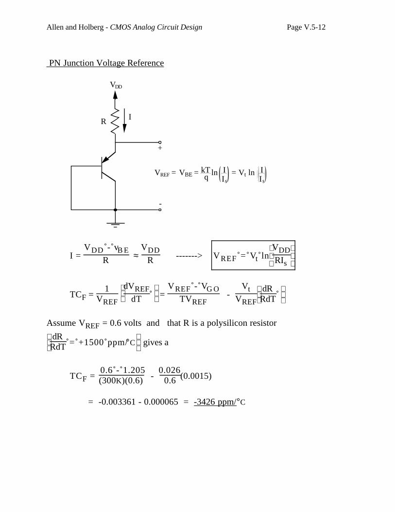
Allen and Holberg - CMOS Analog Circuit Design Page V.5-12
PN Junction Voltage Reference
IR
VDD
+
-
VREF = VBE = kTq ln I
Is = Vt ln I
Is
I = VDD - vB E
R ≈ VDD
R -------> VREF = Vt ln
VDD
RIs
TCF = 1
VREF
dVREF
dT = VREF - VG O
TVREF -
VtVREF
dR
RdT
Assume VREF = 0.6 volts and that R is a polysilicon resistor
dR
RdT = +1500 ppm/°C gives a
TCF = 0.6 - 1.205(300K)(0.6) -
0.0260.6 (0.0015)
= -0.003361 - 0.000065 = -3426 ppm/ °C
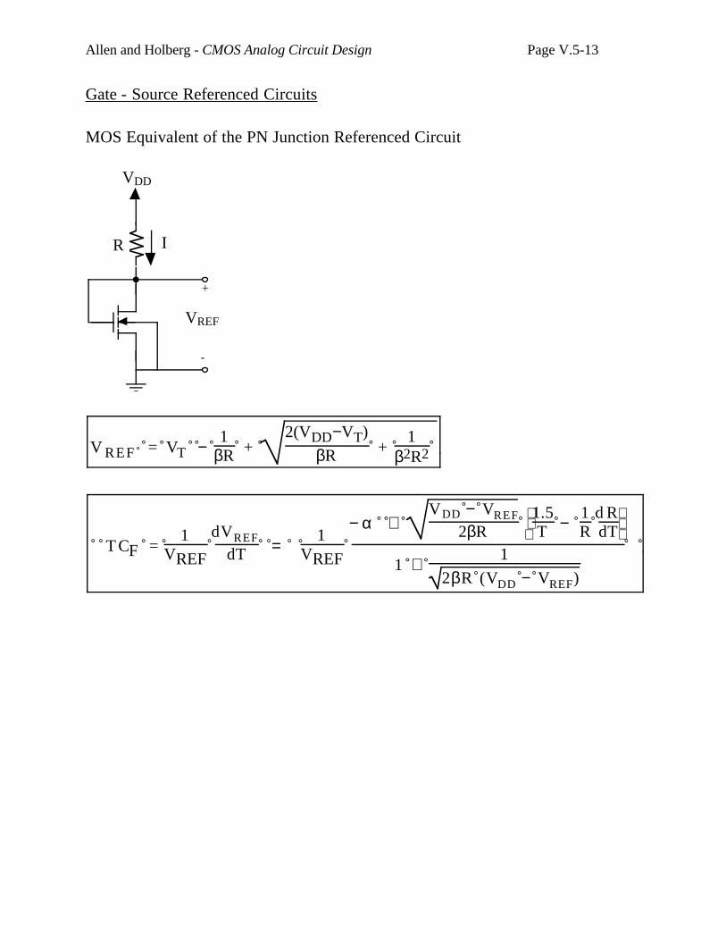
Allen and Holberg - CMOS Analog Circuit Design Page V.5-13
Gate - Source Referenced Circuits
MOS Equivalent of the PN Junction Referenced Circuit
R I
VREF
+
-
VDD
V REF = VT − 1
βR + 2(VDD−VT)
βR + 1
β2R2
T C F = 1
VREF dVREF
dT = 1
VREF − α +
VDD − VREF
2βR
1.5
T − 1R
d RdT
1 + 1
2βR (VDD − VREF)
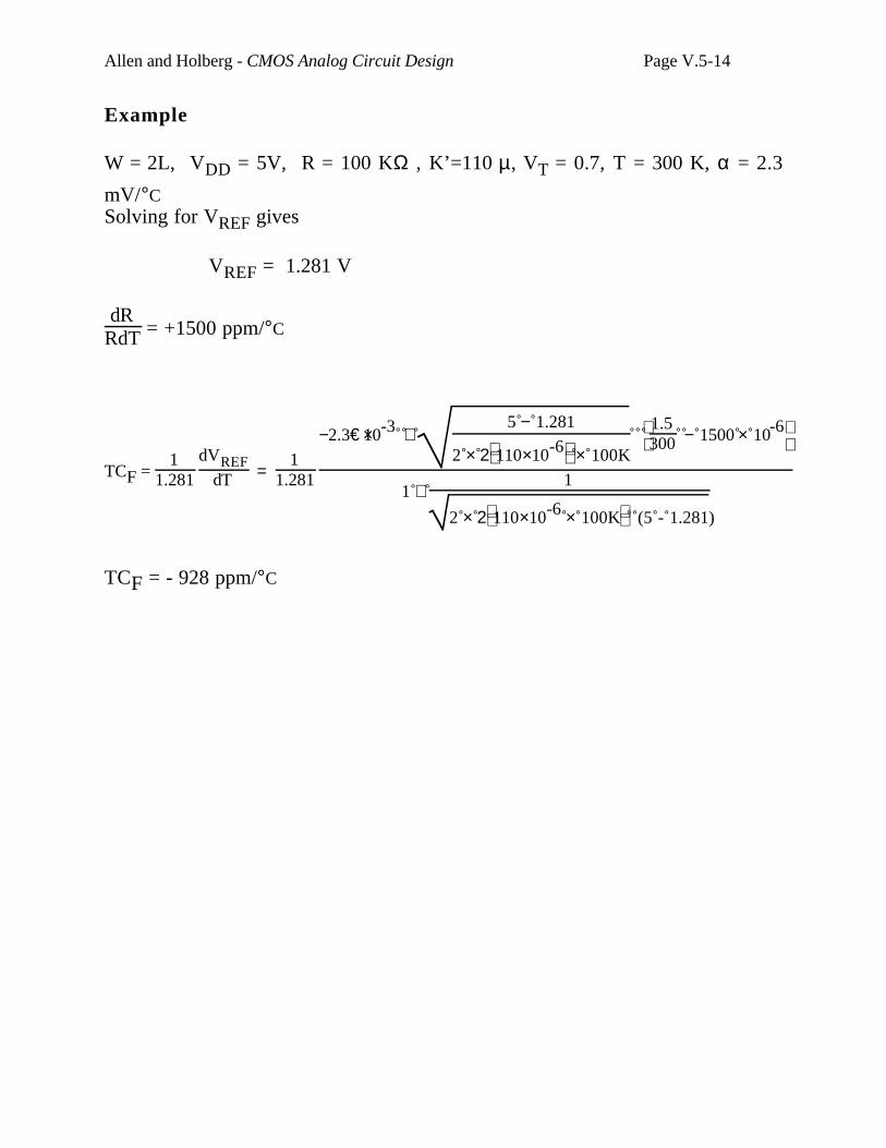
Allen and Holberg - CMOS Analog Circuit Design Page V.5-14
Example
W = 2L, VDD = 5V, R = 100 KΩ , K’=110 µ, VT = 0.7, T = 300 K, α = 2.3
mV/°CSolving for VREF gives
VREF = 1.281 V
dRRdT = +1500 ppm/°C
TCF = 1
1.281 dVREF
dT = 1
1.281
−2.3€×10-3 + 5 − 1.281
2 × 2 110×10-6 × 100K
1.5
300 − 1500 × 10-6
1 + 1
2 × 2 110×10-6 × 100K (5 - 1.281)
TCF = - 928 ppm/°C
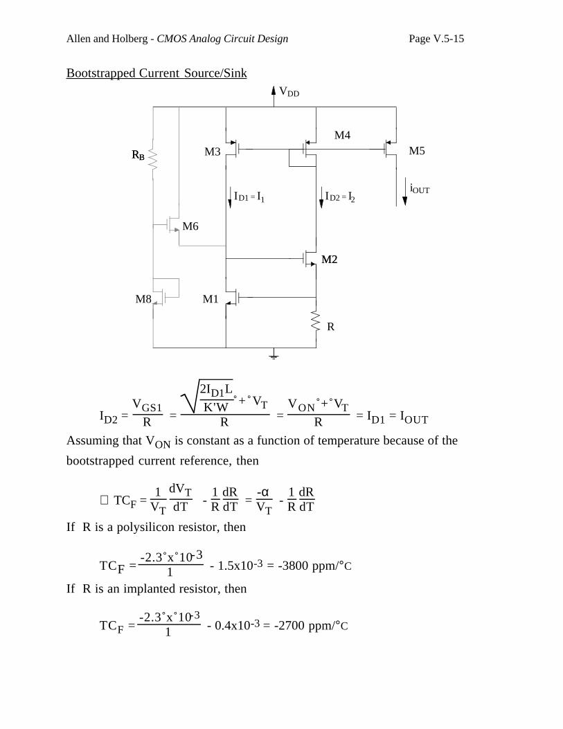
Allen and Holberg - CMOS Analog Circuit Design Page V.5-15
Bootstrapped Current Source/Sink
M5
ID2
M2
R
ID1
M6
RB
iOUT
M2
M3
VDD
RB
I1 = I2=
M4
M1M8
ID2 = VGS1
R =
2ID1L
K'W + VT
R = VON + VT
R = ID1 = IOUT
Assuming that VON is constant as a function of temperature because of the
bootstrapped current reference, then
∴ TCF = 1
VT dVTdT -
1R
dRdT =
-αVT
- 1R
dRdT
If R is a polysilicon resistor, then
TCF = -2.3 x 10⁻³
1 - 1.5x10-3 = -3800 ppm/°C
If R is an implanted resistor, then
TCF = -2.3 x 10⁻³
1 - 0.4x10-3 = -2700 ppm/°C
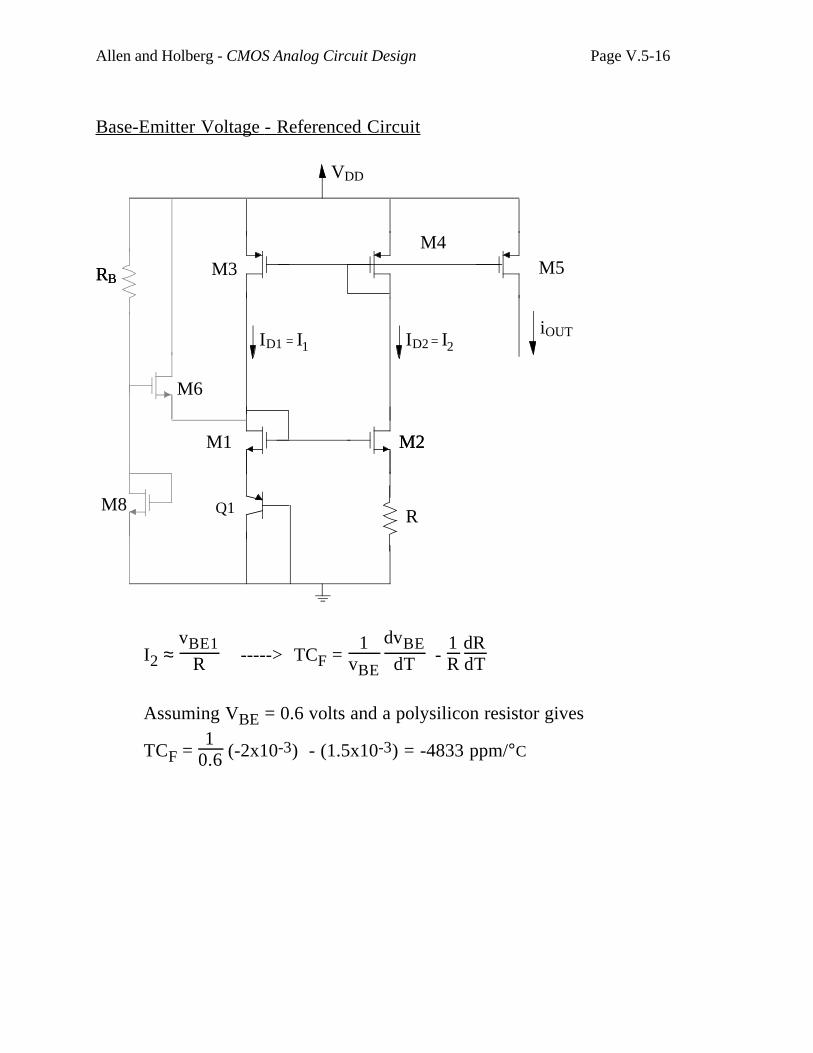
Allen and Holberg - CMOS Analog Circuit Design Page V.5-16
Base-Emitter Voltage - Referenced Circuit
M5
ID2
M2
R
ID1
M6
RB
iOUT
M2
M3
VDD
RB
I1 = I2=
M4
M1
M8 Q1
I2 ≈ vBE1
R -----> TCF = 1
vBE dvBE
dT - 1R
dRdT
Assuming VBE = 0.6 volts and a polysilicon resistor gives
TCF = 1
0.6 (-2x10⁻³) - (1.5x10⁻³) = -4833 ppm/°C
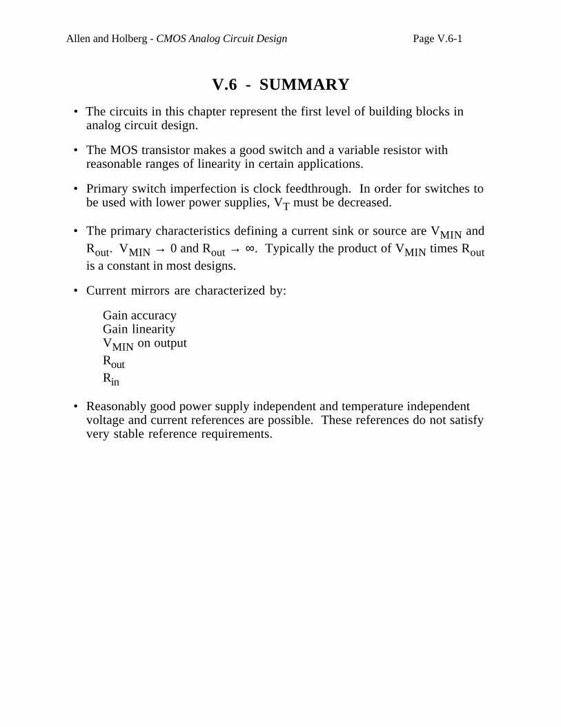
Allen and Holberg - CMOS Analog Circuit Design Page V.6-1
V.6 - SUMMARY
• The circuits in this chapter represent the first level of building blocks inanalog circuit design.
• The MOS transistor makes a good switch and a variable resistor withreasonable ranges of linearity in certain applications.
• Primary switch imperfection is clock feedthrough. In order for switches tobe used with lower power supplies, VT must be decreased.
• The primary characteristics defining a current sink or source are VMIN andRout. VMIN → 0 and Rout → ∞. Typically the product of VMIN times Routis a constant in most designs.
• Current mirrors are characterized by:
Gain accuracyGain linearityVMIN on outputRoutRin
• Reasonably good power supply independent and temperature independentvoltage and current references are possible. These references do not satisfyvery stable reference requirements.
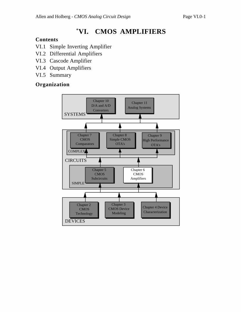
Allen and Holberg - CMOS Analog Circuit Design Page VI.0-1
VI. CMOS AMPLIFIERSContentsVI.1 Simple Inverting AmplifierVI.2 Differential AmplifiersVI.3 Cascode AmplifierVI.4 Output AmplifiersVI.5 Summary
Organization
DEVICES
SYSTEMS
CIRCUITS
Chapter 2 CMOS
Technology
Chapter 3 CMOS Device
Modeling
Chapter 4 Device Characterization
Chapter 7 CMOS
Comparators
Chapter 8 Simple CMOS
OTA's
Chapter 9 High Performance
OTA's
Chapter 5 CMOS
Subcircuits
Chapter 6 CMOS
Amplifiers
Chapter 10D/A and A/D Converters
Chapter 11Analog Systems
SIMPLE
COMPLEX
Allen and Holberg - CMOS Analog Circuit Design Page VI.1-1
VI.1 SIMPLE INVERTING AMPLIFIERS
CHARACTERIZATION OF AMPLIFIERS
We shall characterize the amplifiers of this Chapter by the followingaspects:
• Large Signal Voltage Transfer Characteristics
• Maximum Signal Swing Limits
• Small Signal Midband Performance
Gain
Input resistance
Output resistance
• Small Signal Frequency Response
• Other Considerations
Noise
Power
Etc.
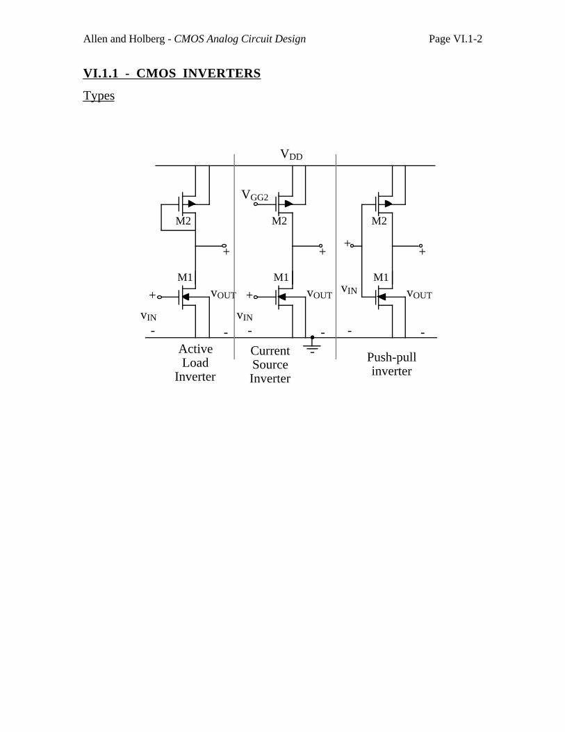
Allen and Holberg - CMOS Analog Circuit Design Page VI.1-2
VI.1.1 - CMOS INVERTERS
Types
VDD
M1
M2
+
-vIN
+
-
vOUT
M1
M2
+
-vIN
+
-
vOUT
M1
M2
+
-
vIN
+
-
vOUT
VGG2
Active Load
Inverter
Current Source Inverter
Push-pull inverter
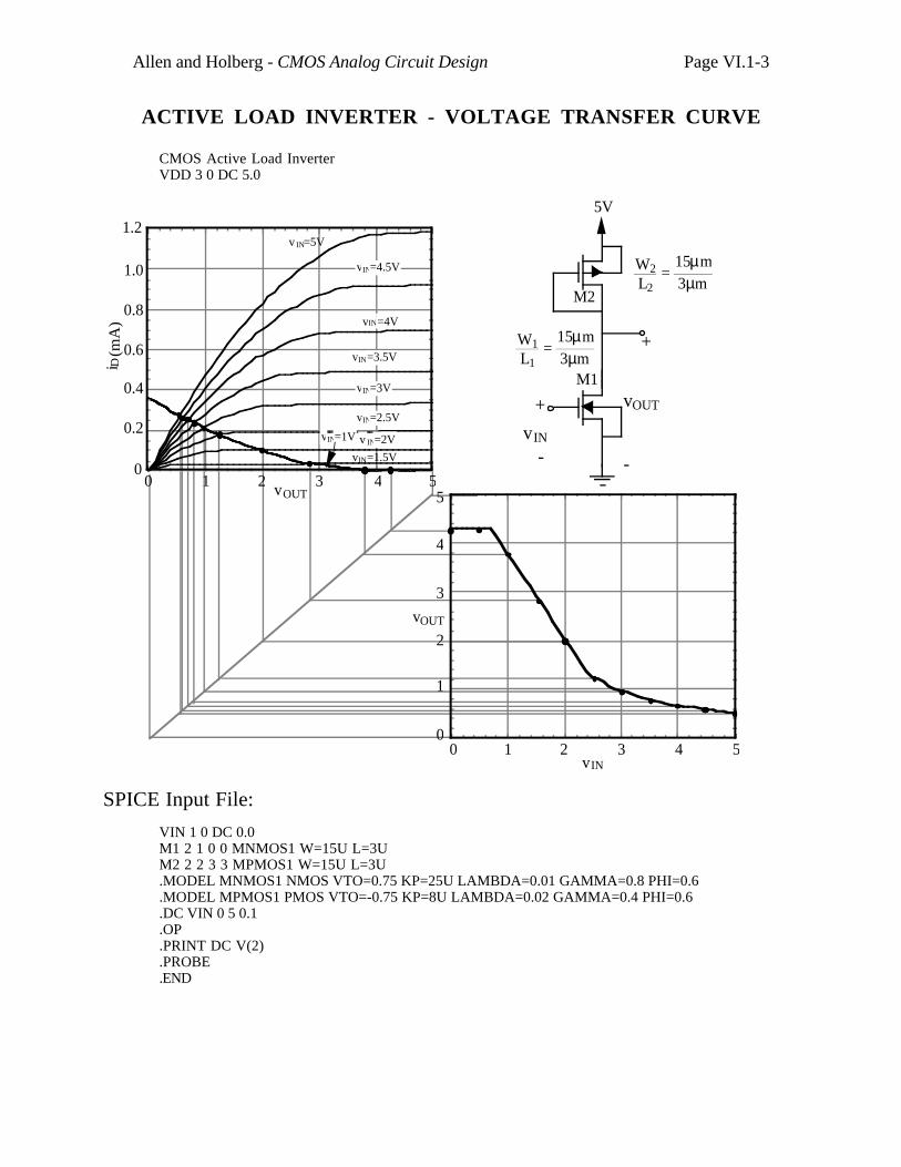
Allen and Holberg - CMOS Analog Circuit Design Page VI.1-3
ACTIVE LOAD INVERTER - VOLTAGE TRANSFER CURVE
CMOS Active Load InverterVDD 3 0 DC 5.0
VIN 1 0 DC 0.0M1 2 1 0 0 MNMOS1 W=15U L=3UM2 2 2 3 3 MPMOS1 W=15U L=3U.MODEL MNMOS1 NMOS VTO=0.75 KP=25U LAMBDA=0.01 GAMMA=0.8 PHI=0.6.MODEL MPMOS1 PMOS VTO=-0.75 KP=8U LAMBDA=0.02 GAMMA=0.4 PHI=0.6.DC VIN 0 5 0.1.OP.PRINT DC V(2).PROBE.END
0
1
2
3
4
5
0 1 2 3 4 5
vOUT
vIN
M1
M2
+
-vIN
+
-
vOUT
5V
W2L2
= 15µm3µm
W1L1
= 15µm3µm
0
0.2
0.4
0.6
0.8
1.0
1.2
0 1 2 3 4 5
vIN=4.5V
v IN=5V
vIN=4V
vIN=3.5V
vIN=3V
vIN=2.5V
v IN=2V
vIN=1.5V
vIN=1V
vOUT
i D(m
A)
SPICE Input File:
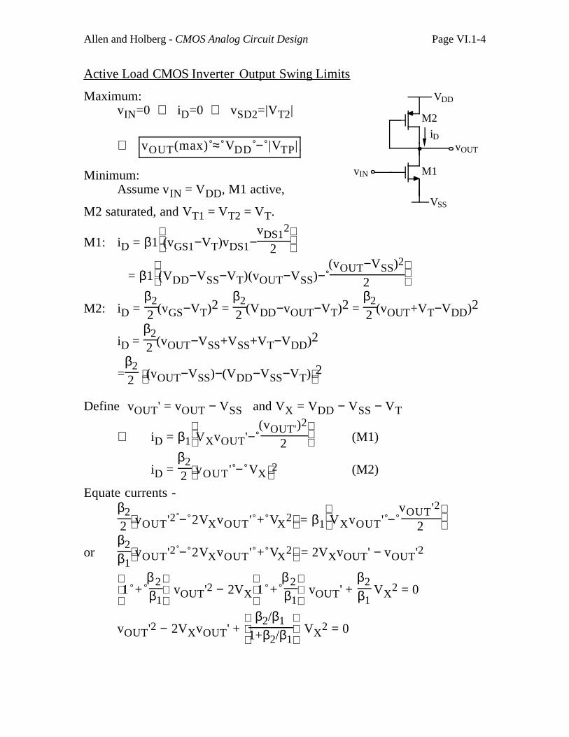
Allen and Holberg - CMOS Analog Circuit Design Page VI.1-4
Active Load CMOS Inverter Output Swing Limits
Maximum:vIN=0 ⇒ iD=0 ⇒ vSD2=|VT2|
∴ vOUT(max) ≈ VDD − |VTP|
Minimum:Assume vIN = VDD, M1 active,
M2 saturated, and VT1 = VT2 = VT.
M1: iD = β1
(vGS1−VT)vDS1−vDS1
2
2
= β1
(VDD−VSS−VT)(vOUT−VSS)− (vOUT−VSS)2
2
M2: iD = β22 (vGS−VT)2 =
β22 (VDD−vOUT−VT)2 =
β22 (vOUT+VT−VDD)2
iD = β22 (vOUT−VSS+VSS+VT−VDD)2
=β22 (vOUT−VSS)−(VDD−VSS−VT) 2
Define vOUT' = vOUT − VSS and VX = VDD − VSS − VT
∴ iD = β1
VXvOUT'− (vOUT')2
2 (M1)
iD = β22 vOUT' − VX
2 (M2)
Equate currents -β22 vOUT'2 − 2VXvOUT' + VX
2 = β1
VXvOUT' − vOUT'2
2
or β2β1 vOUT'2 − 2VXvOUT' + VX
2 = 2VXvOUT' − vOUT'2
1 + β2β1
vOUT'2 − 2VX
1 + β2β1
vOUT' + β2β1
VX2 = 0
vOUT'2 − 2VXvOUT' +
β2/β1
1+β2/β1 VX
2 = 0
M1
M2
vIN
vOUT
iD
VDD
VSS
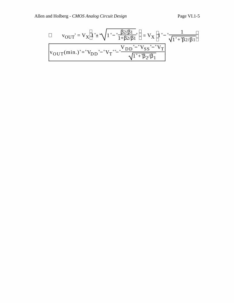
Allen and Holberg - CMOS Analog Circuit Design Page VI.1-5
∴ vOUT' = VX
1 ± 1 − β2/β1
1+β2/β1 = VX
1 −
1
1 + β2/β1
vOUT(min.) = VDD − VT − V DD − VSS − VT
1 + β2/β1
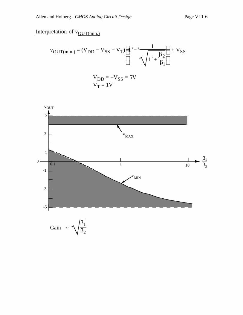
Allen and Holberg - CMOS Analog Circuit Design Page VI.1-6
Interpretation of v OUT(min.)
vOUT(min.) = (VDD − VSS − VT)
1 −
1
1 + β2β1
+ VSS
VDD = −VSS = 5VVT = 1V
v
-5
-3
3
5
01 10
OUT
-1
1
0.1β
2β1
vMAX
vMIN
Gain ~ β1β2
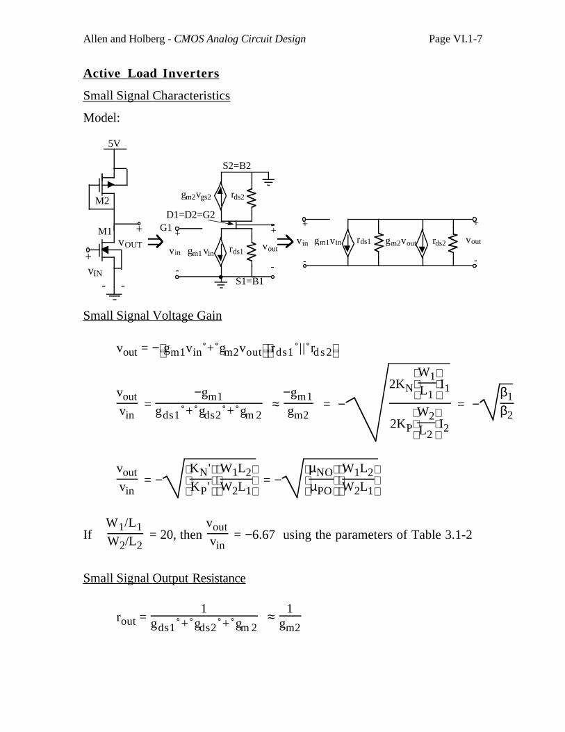
Allen and Holberg - CMOS Analog Circuit Design Page VI.1-7
Active Load Inverters
Small Signal Characteristics
Model:
gm1 vinvin
+
-
gm2vgs2 rds2
rds1
+
-
vout
S2=B2
D1=D2=G2G1
S1=B1
gm1vin
+
-
rds1
+
-
voutvin gm2vout rds2
M1
M2
+
-vIN
+
-
vOUT
5V
Small Signal Voltage Gain
vout = − gm1vin + gm2vout rds1 || rd s 2
voutvin
= −gm1
gds1 + gds2 + gm 2 ≈
−gm1gm2
= −2KN
W1
L1I1
2KP
W2
L2I2
= −β1β2
voutvin
= −
KN'
KP'
W1L2
W2L1 = −
µNO
µPO
W1L2
W2L1
If W1/L1W2/L2
= 20, then voutvin
= −6.67 using the parameters of Table 3.1-2
Small Signal Output Resistance
rout = 1
gds1 + gds2 + gm 2 ≈
1gm2
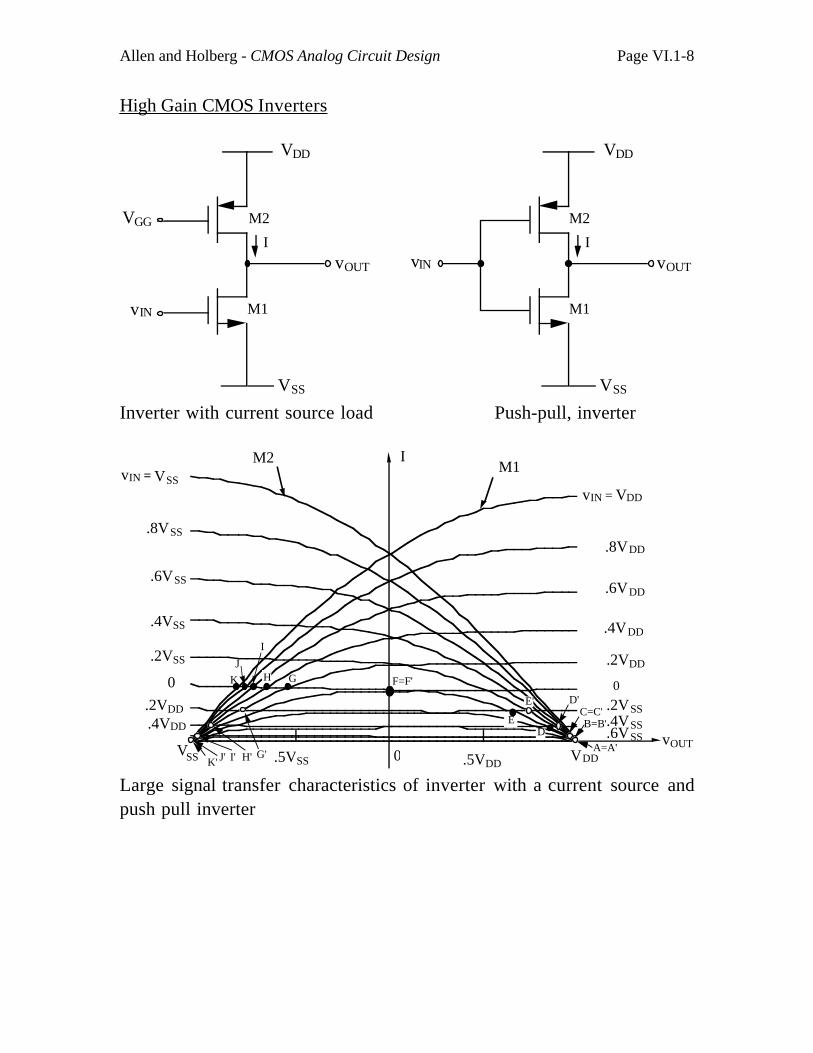
Allen and Holberg - CMOS Analog Circuit Design Page VI.1-8
High Gain CMOS Inverters
vOUT
M1
M2
I
VDD
VSS
VGG
vIN
vOUT
M1
M2
I
VDD
VSS
vIN
Inverter with current source load Push-pull, inverter
VSS
vIN
VSS .5VSS
.8VSS
.6VSS
.4VSS
.2VSS
.4VDD
.6VDD
.8VDD
VDD
VDD.5VDD
=
.2VDD
.4VDD
.2VSS
.4VSS
.6VSS
0
.2VDD
0
0
IvIN =
M1M2
vOUT
F=F'
C=C'
G'H'
B=B'
GH
I
J
K
J' I'K'A=A'
E
E'
D
D'
Large signal transfer characteristics of inverter with a current source andpush pull inverter
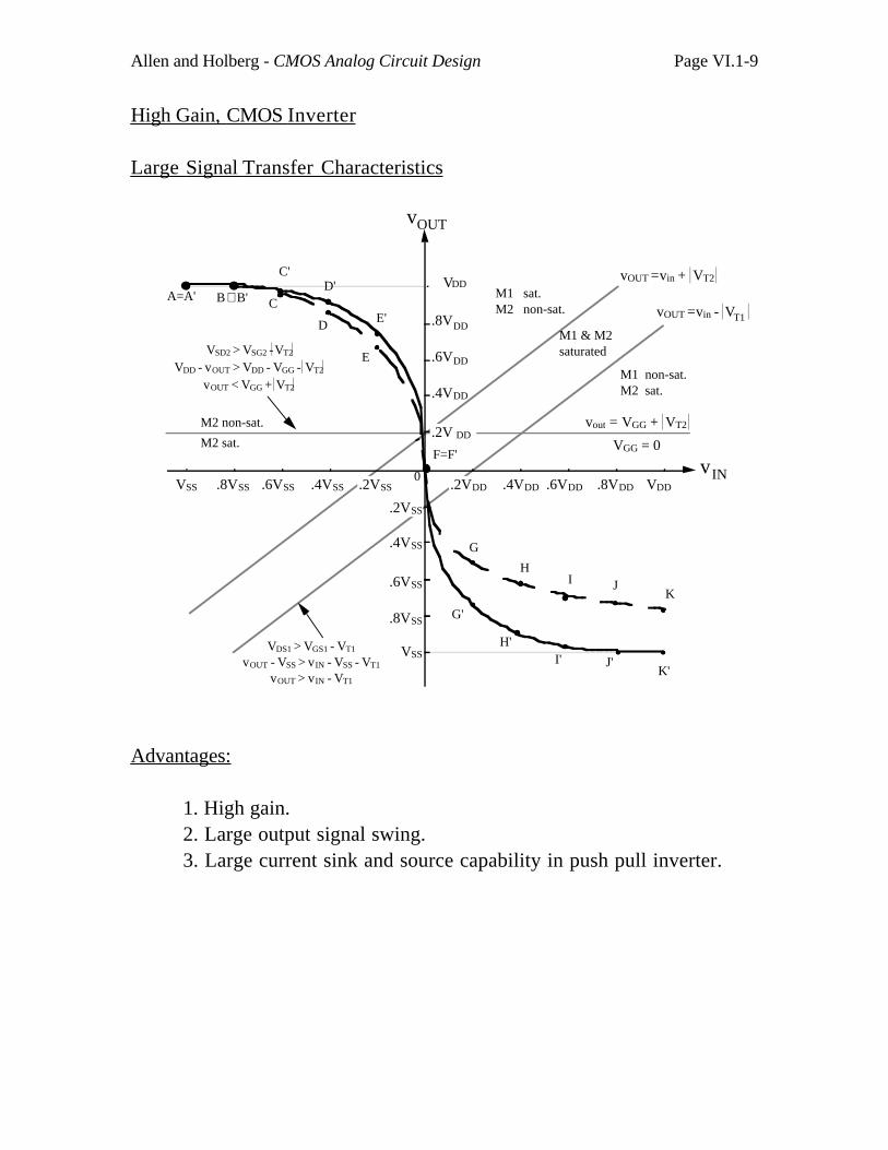
Allen and Holberg - CMOS Analog Circuit Design Page VI.1-9
High Gain, CMOS Inverter
Large Signal Transfer Characteristics
vOUT
.2V DD
.6VDD
.8VDD
VDD
F=F'vIN
A=A'
C'
CB ≅ B'
D
D'
E
E'
0
M1 sat.M2 non-sat.
M1 & M2 saturated
G
G'
H
H'I'
I J
J'
M1 non-sat.M2 sat.
vOUT =vin + VT2
vOUT =vin - VT1
.4VDD
.4VDD.2VDD .6VDD .8VDD VDDVSS
VSS
.8VSS
.8VSS
.6VSS
.6VSS
.4VSS
.4VSS
.2VSS
.2VSS
K
K'
M2 non-sat.
M2 sat.
vout = VGG + VT2
VGG = 0
VSD2 > VSG2 -VT2
VDD - vOUT > VDD - VGG - VT2
vOUT < VGG + VT2
VDS1 > VGS1 - VT1
vOUT - VSS > vIN - VSS - VT1
vOUT vIN - VT1>
Advantages:
1. High gain.2. Large output signal swing.3. Large current sink and source capability in push pull inverter.
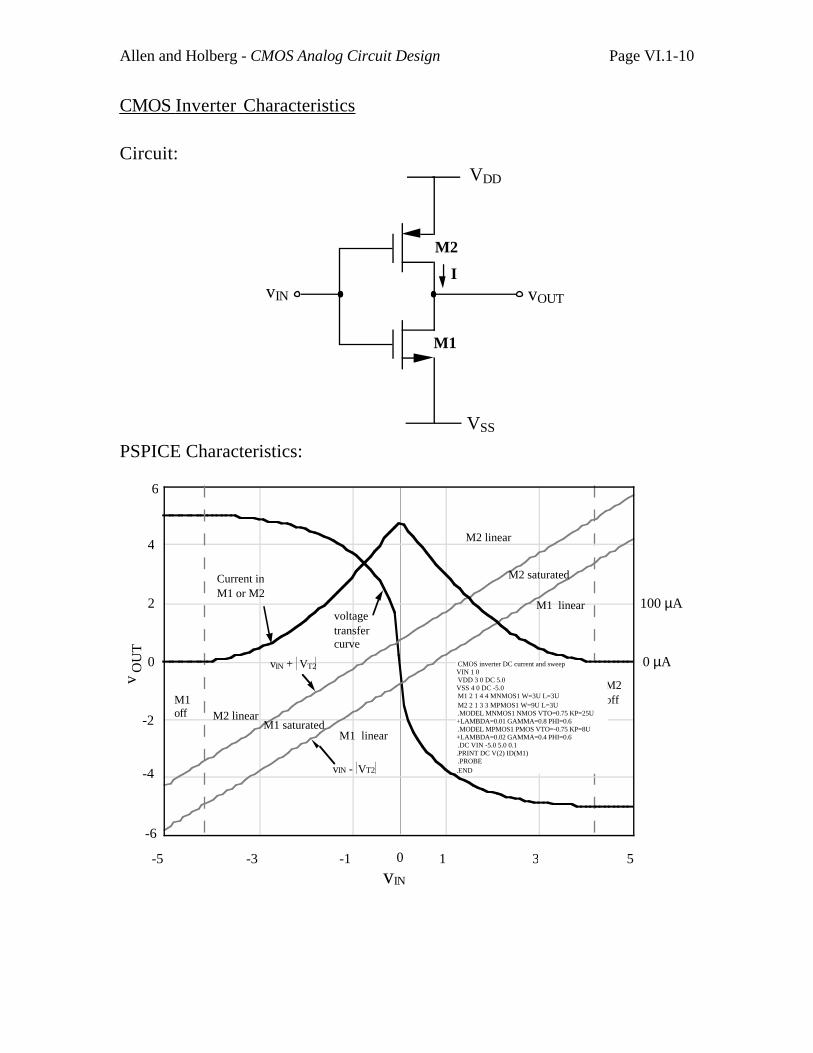
Allen and Holberg - CMOS Analog Circuit Design Page VI.1-10
CMOS Inverter Characteristics
Circuit:
vOUT
M1
M2
I
VDD
VSS
vIN
PSPICE Characteristics:
-6
6
-5 -3 -1 1 3 5
0 µA
100 µA
0
4
2
-2
-4
0
vIN
M2 saturated
M1 saturated
Current inM1 or M2
vIN + VT2
vIN - VT2
M1 off
M1 linear
M2 linear
M2 off
CMOS inverter DC current and sweepVIN 1 0 VDD 3 0 DC 5.0VSS 4 0 DC -5.0M1 2 1 4 4 MNMOS1 W=3U L=3UM2 2 1 3 3 MPMOS1 W=9U L=3U.MODEL MNMOS1 NMOS VTO=0.75 KP=25U+LAMBDA=0.01 GAMMA=0.8 PHI=0.6.MODEL MPMOS1 PMOS VTO=-0.75 KP=8U+LAMBDA=0.02 GAMMA=0.4 PHI=0.6.DC VIN -5.0 5.0 0.1.PRINT DC V(2) ID(M1).PROBE.END
voltage transfercurve
M1 linear
M2 linear
vO
UT
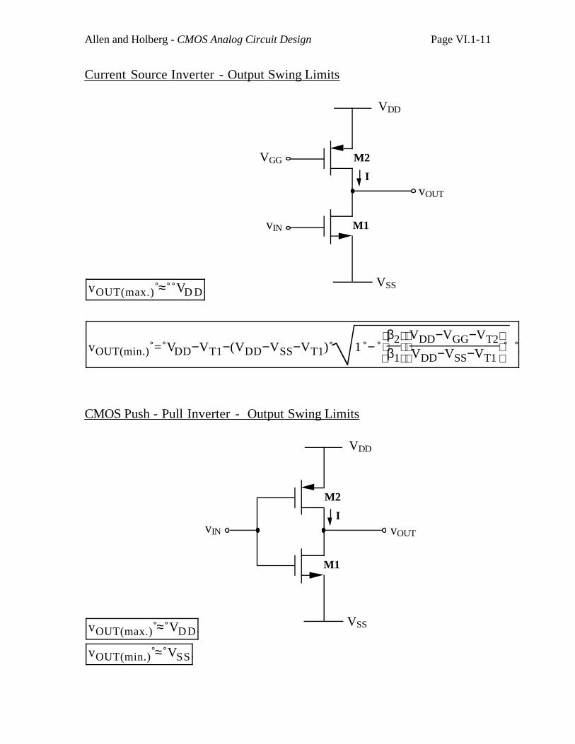
Allen and Holberg - CMOS Analog Circuit Design Page VI.1-11
Current Source Inverter - Output Swing Limits
vOUT(max.) ≈ VD D
vOUT
M1
M2
I
VDD
VSS
VGG
vIN
vOUT(min.) = VDD−VT1−(VDD−VSS−VT1) 1 −
β2
β1
VDD−VGG−VT2
VDD−VSS−VT1
CMOS Push - Pull Inverter - Output Swing Limits
vOUT(max.) ≈ VDD
vOUT
M1
M2
I
VDD
VSS
vIN
vOUT(min.) ≈ VSS
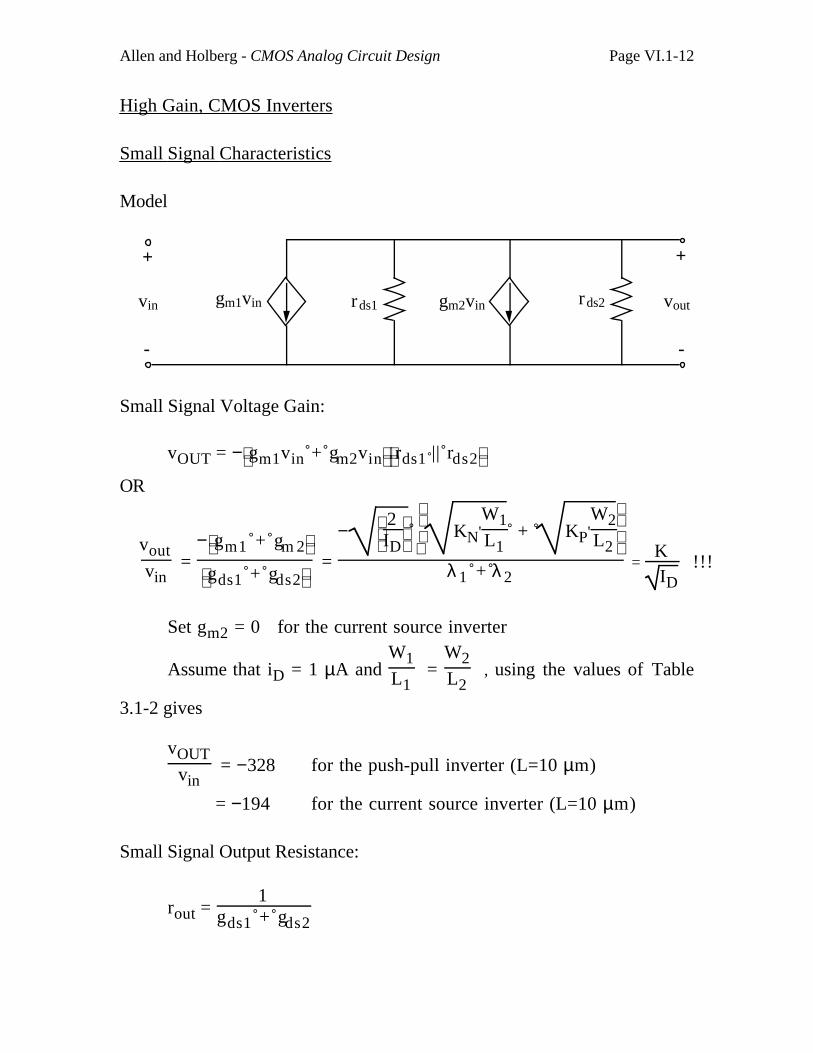
Allen and Holberg - CMOS Analog Circuit Design Page VI.1-12
High Gain, CMOS Inverters
Small Signal Characteristics
Model
gm1vin gm2vinrds1 rds2
+
-
vout
-
+
vin
Small Signal Voltage Gain:
vOUT = − gm1vin + gm2vin rds1 || rds2
OR
voutvin
= − gm1 + gm 2
gds1 + gds2 =
−
2
ID
KN'W1L1
+ KP'W2L2
λ 1 + λ 2 =
KID
!!!
Set gm2 = 0 for the current source inverter
Assume that iD = 1 µA and W1L1
= W2L2
, using the values of Table
3.1-2 gives
vOUTvin
= −328 for the push-pull inverter (L=10 µm)
= −194 for the current source inverter (L=10 µm)
Small Signal Output Resistance:
rout = 1
gds1 + gds2
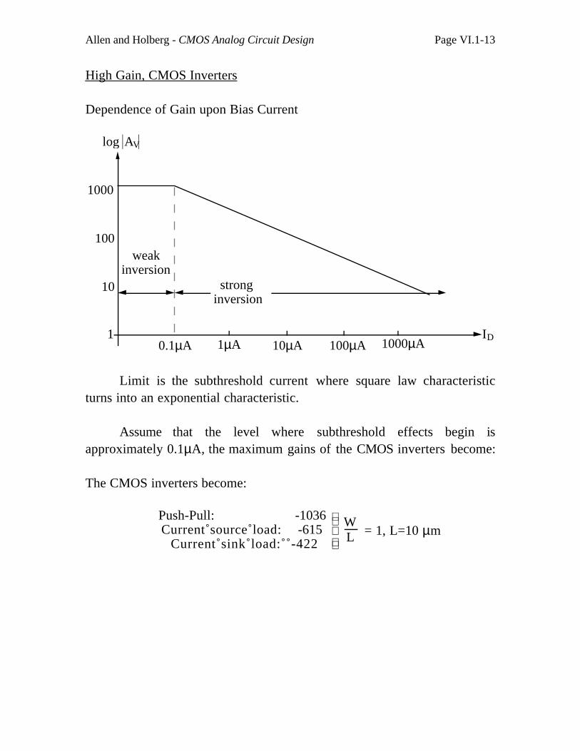
Allen and Holberg - CMOS Analog Circuit Design Page VI.1-13
High Gain, CMOS Inverters
Dependence of Gain upon Bias Current
log AV
1000
1
100
10
weak inversion
stronginversion
0.1µA 1µA 10µA 100µA 1000µAID
Limit is the subthreshold current where square law characteristicturns into an exponential characteristic.
Assume that the level where subthreshold effects begin isapproximately 0.1µA, the maximum gains of the CMOS inverters become:
The CMOS inverters become:
Push-Pull: -1036
Current source load: -615Current sink load: -422
WL = 1, L=10 µm
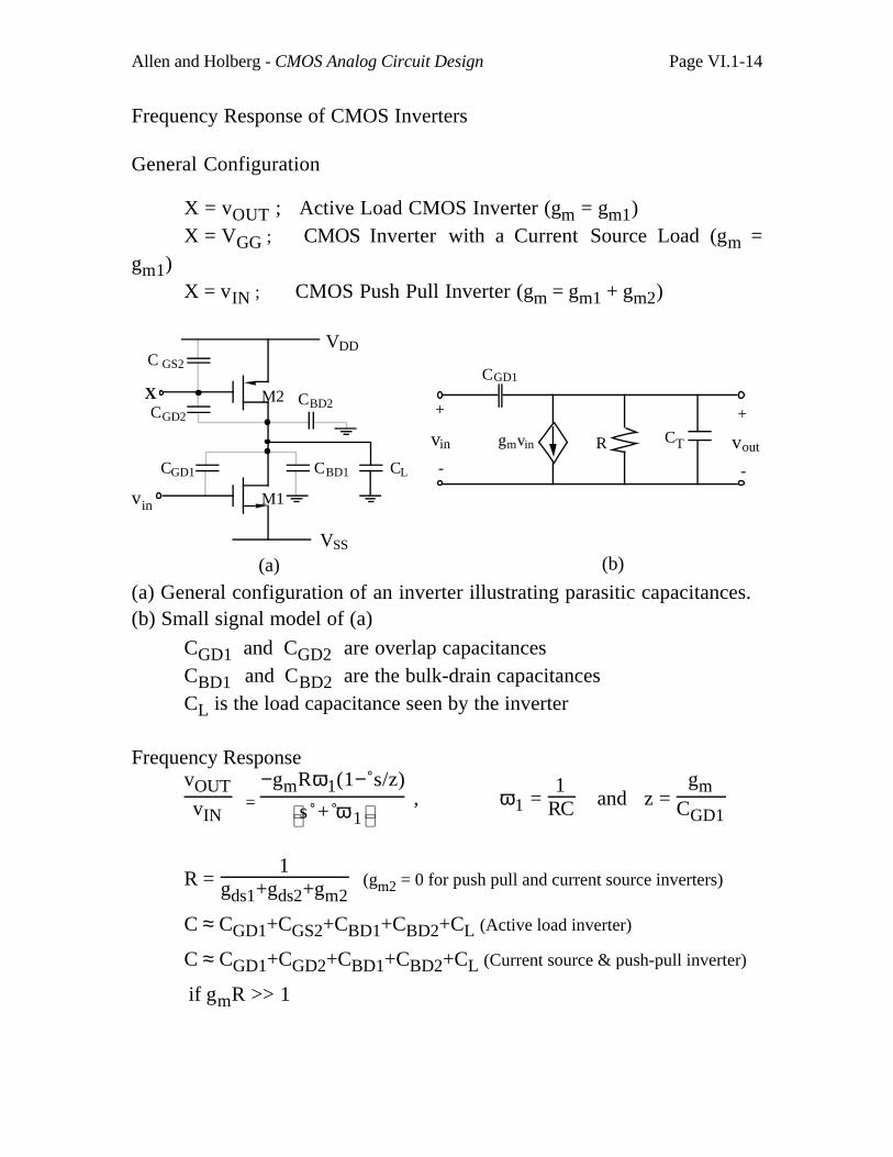
Allen and Holberg - CMOS Analog Circuit Design Page VI.1-14
Frequency Response of CMOS Inverters
General Configuration
X = vOUT ; Active Load CMOS Inverter (gm = gm1)X = VGG ; CMOS Inverter with a Current Source Load (gm =
gm1)X = vIN ; CMOS Push Pull Inverter (gm = gm1 + gm2)
(b)(a)
CLCBD1CGD1
CGD2CBD2M2
M1
VDD
VSS
X
C GS2
vin
R CTgmvin
+
-
vin
+
-
vout
CGD1
(a) General configuration of an inverter illustrating parasitic capacitances.(b) Small signal model of (a)
CGD1 and CGD2 are overlap capacitancesCBD1 and CBD2 are the bulk-drain capacitancesCL is the load capacitance seen by the inverter
Frequency ResponsevOUTvIN
= −gmRω1(1− s/z)
s + ω1 , ω1 =
1RC and z =
gmCGD1
R = 1
gds1+gds2+gm2 (gm2 = 0 for push pull and current source inverters)
C ≈ CGD1+CGS2+CBD1+CBD2+CL (Active load inverter)
C ≈ CGD1+CGD2+CBD1+CBD2+CL (Current source & push-pull inverter)
if gmR >> 1
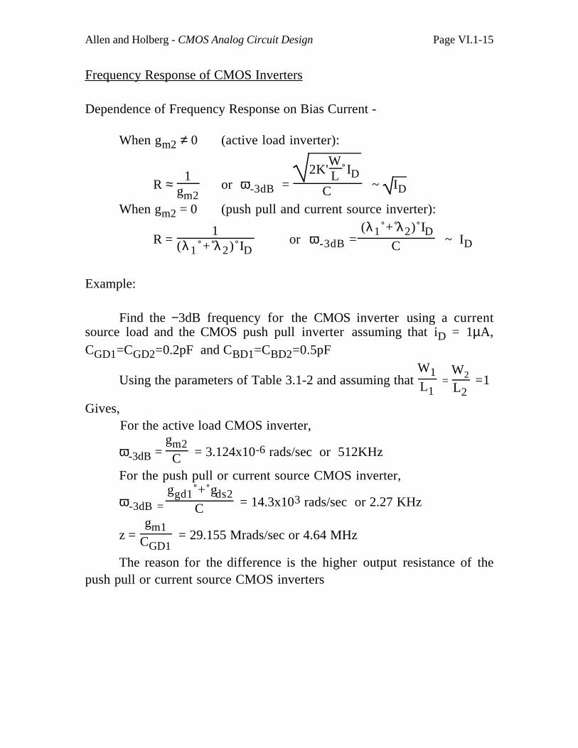
Allen and Holberg - CMOS Analog Circuit Design Page VI.1-15
Frequency Response of CMOS Inverters
Dependence of Frequency Response on Bias Current -
When gm2 ≠ 0 (active load inverter):
R ≈ 1
gm2 or ω-3dB =
2K'WL ID
C ~ ID
When gm2 = 0 (push pull and current source inverter):
R = 1
(λ 1 + λ 2) ID or ω-3dB =
(λ1 + λ2) IDC ~ ID
Example:
Find the −3dB frequency for the CMOS inverter using a currentsource load and the CMOS push pull inverter assuming that iD = 1µA,CGD1=CGD2=0.2pF and CBD1=CBD2=0.5pF
Using the parameters of Table 3.1-2 and assuming that W1L1
= W2
L2 =1
Gives,For the active load CMOS inverter,
ω-3dB = gm2
C = 3.124x10⁻⁶ rads/sec or 512KHz
For the push pull or current source CMOS inverter,
ω-3dB = ggd1 + gds2
C = 14.3x10³ rads/sec or 2.27 KHz
z = gm1
CGD1 = 29.155 Mrads/sec or 4.64 MHz
The reason for the difference is the higher output resistance of thepush pull or current source CMOS inverters
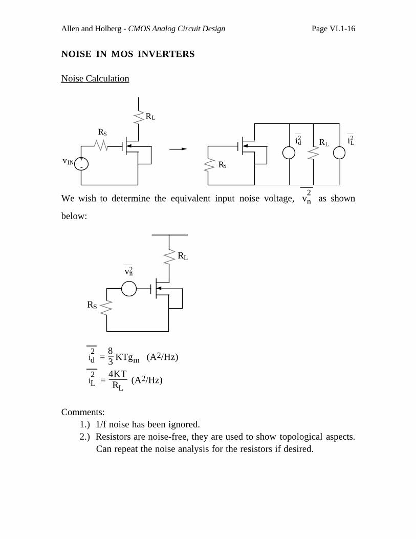
Allen and Holberg - CMOS Analog Circuit Design Page VI.1-16
NOISE IN MOS INVERTERS
Noise Calculation
+-
RS
RL
vIN
id2 iL
2RL
RS
We wish to determine the equivalent input noise voltage, v2n as shown
below:
RS
RL
vn2
i2d =
83 KTgm (A2/Hz)
i2L =
4KTRL
(A2/Hz)
Comments:1.) 1/f noise has been ignored.2.) Resistors are noise-free, they are used to show topological aspects. Can repeat the noise analysis for the resistors if desired.
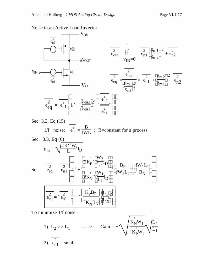
Allen and Holberg - CMOS Analog Circuit Design Page VI.1-17
Noise in an Active Load Inverter
e2out
vIN=0 = e
2n1
gm1
gm2 2 + e
2n2
e2eq =
e2out
gm1
gm2
2
= e2n1 +
gm2
gm1 2 e
2n2
e2eq = e
2n1
1 +
gm2
gm1
2
e
2n2
e2n1
Sec 3.2, Eq (15)
1/f noise: e2n =
BfWL ; B=constant for a process
Sec. 3.3, Eq (6)
gm = 2K' W
L ID
So e2eq = e
2n1
1 +
2K'P
W2
L2ID
2K'N
W1
L1ID
BP
fW2L2
fW1L1
BN
e2eq = e
2n1
1 +
K
'PBP
K'NBN
L1
L2
2
To minimize 1/f noise -
1). L2 >> L1 -----> Gain = −K
'NW1
K'PW2
L2L1
2). e2n1 small
M2
M1
VDD
VSS
vIN
vOUT
en12
en22
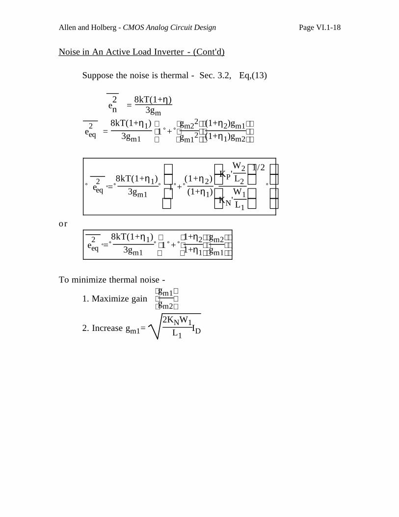
Allen and Holberg - CMOS Analog Circuit Design Page VI.1-18
Noise in An Active Load Inverter - (Cont'd)
Suppose the noise is thermal - Sec. 3.2, Eq,(13)
e2n =
8kT(1+η)3gm
e2eq =
8kT(1+η1)
3gm1
1 +
gm2
2
gm12
(1+η2)gm1
(1+η1)gm2
e2eq =
8kT(1+η1)
3gm1
1 + (1+η2)
(1+η1)
KP'
W2L2
KN'W1L1
1/2
or
e2eq =
8kT(1+η1)
3gm1
1 +
1+η2
1+η1
gm2
gm1
To minimize thermal noise -
1. Maximize gain
gm1
gm2
2. Increase gm1= 2KNW1
L1ID
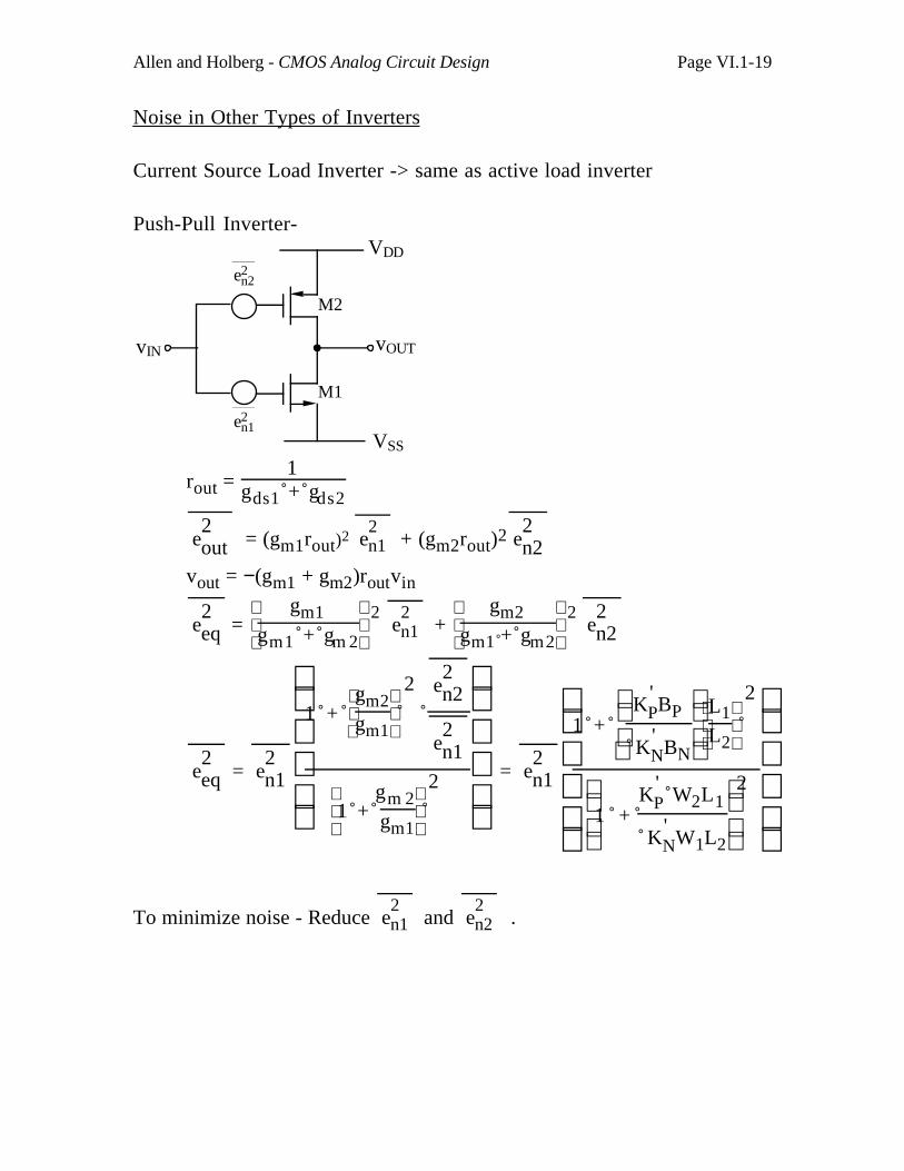
Allen and Holberg - CMOS Analog Circuit Design Page VI.1-19
Noise in Other Types of Inverters
Current Source Load Inverter -> same as active load inverter
Push-Pull Inverter-
M2
M1
VDD
VSS
vIN vOUT
en12
en22
rout = 1
gds1 + gds2
e2out = (gm1rout)
2 e2n1 + (gm2rout)2 e
2n2
vout = −(gm1 + gm2)routvin
e2eq =
gm1
gm1 + gm 2 2 e
2n1
+
gm2
gm1 + gm2 2
e2n2
e2eq = e
2n1
1 +
gm2
gm1
2
e2n2
e2n1
1 + gm 2gm1
2 = e2n1
1 +
K
'PBP
K'NBN
L1
L2
2
1 +
K'P W2L1
K'NW1L2
2
To minimize noise - Reduce e2n1 and e
2n2 .
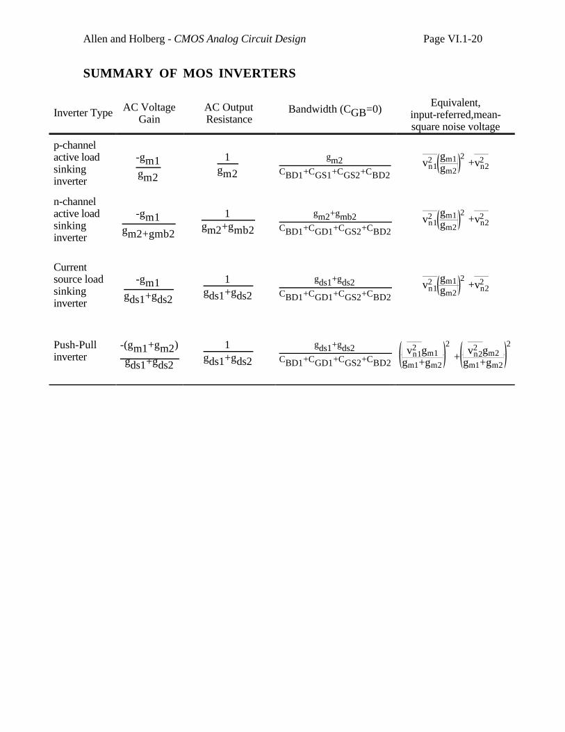
Allen and Holberg - CMOS Analog Circuit Design Page VI.1-20
SUMMARY OF MOS INVERTERS
Inverter Type AC VoltageGain
AC OutputResistance
Bandwidth (CGB=0)Equivalent,
input-referred,mean-square noise voltage
p-channelactive loadsinkinginverter
-gm1gm2
1
gm2
gm2CBD1+CGS1+CGS2+CBD2
vn12 gm1
gm2
2 +vn2
2
n-channelactive loadsinkinginverter
-gm1gm2+gmb2
1
gm2+gmb2
gm2+gmb2CBD1+CGD1+CGS2+CBD2
vn12 gm1
gm2
2 +vn2
2
Currentsource loadsinkinginverter
-gm1gds1+gds2
1
gds1+gds2
gds1+gds2CBD1+CGD1+CGS2+CBD2
vn12 gm1
gm2
2 +vn2
2
Push-Pullinverter
-(gm1+gm2)
gds1+gds2
1gds1+gds2
gds1+gds2
CBD1+CGD1+CGS2+CBD2 vn1
2 gm1gm1+gm2
2
+
vn22 gm2
gm1+gm2
2
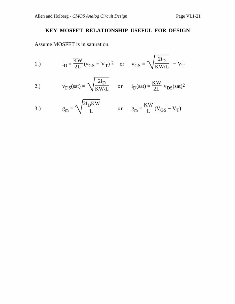
Allen and Holberg - CMOS Analog Circuit Design Page VI.1-21
KEY MOSFET RELATIONSHIP USEFUL FOR DESIGN
Assume MOSFET is in saturation.
1.) iD = KW2L (vGS − VT) 2 or vGS =
2iDKW/L − VT
2.) vDS(sat) = 2iD
KW/L or iD(sat) = KW2L vDS(sat)2
3.) gm = 2IDKW
L or gm = KW
L (VGS − VT)
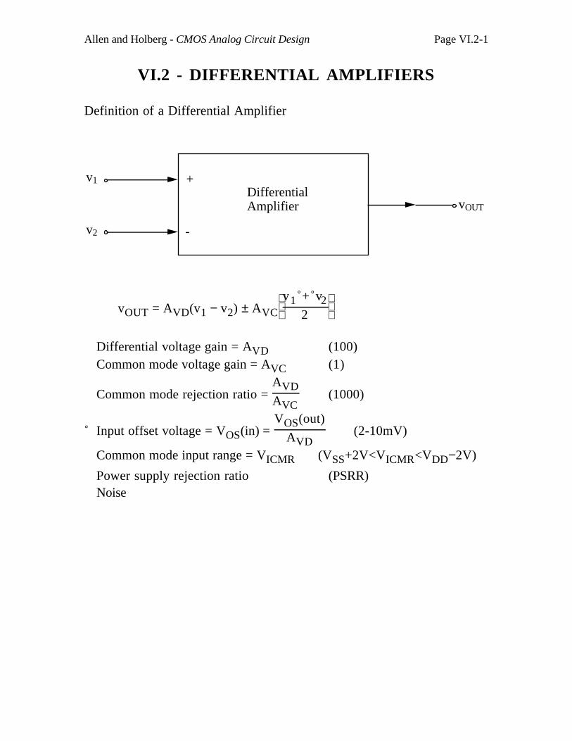
Allen and Holberg - CMOS Analog Circuit Design Page VI.2-1
VI.2 - DIFFERENTIAL AMPLIFIERS
Definition of a Differential Amplifier
DifferentialAmplifier
+
-
v1
v2
vOUT
vOUT = AVD(v1 − v2) ± AVC
v1 + v2
2
Differential voltage gain = AVD (100)Common mode voltage gain = AVC (1)
Common mode rejection ratio = AVDAVC
(1000)
Input offset voltage = VOS(in) = VOS(out)
AVD (2-10mV)
Common mode input range = VICMR (VSS+2V<VICMR<VDD−2V)
Power supply rejection ratio (PSRR)Noise
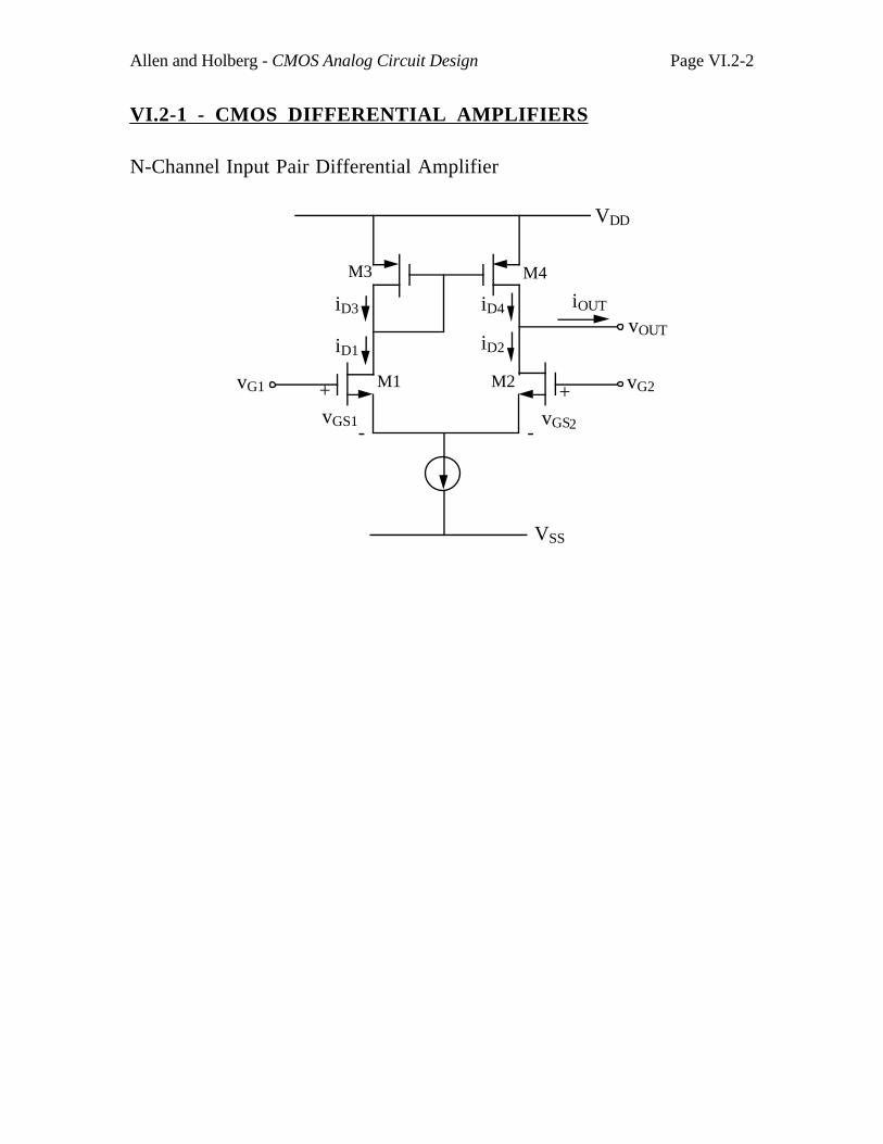
Allen and Holberg - CMOS Analog Circuit Design Page VI.2-2
VI.2-1 - CMOS DIFFERENTIAL AMPLIFIERS
N-Channel Input Pair Differential Amplifier
+
-vGS
M2 vG2
VDD
VSS
iOUT
vOUT
iD3
iD1
M1
M3 M4
iD4
iD2
vG1
vGS1
+
- 2
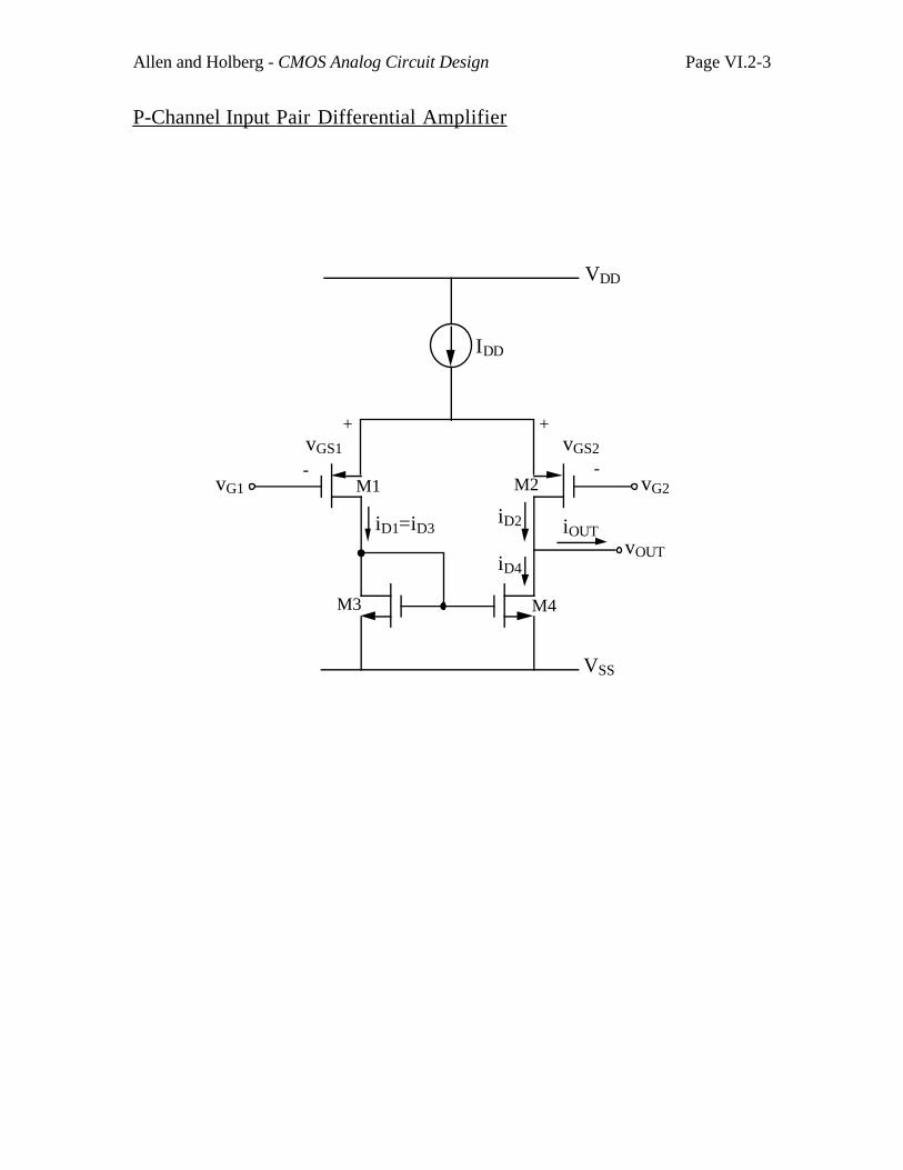
Allen and Holberg - CMOS Analog Circuit Design Page VI.2-3
P-Channel Input Pair Differential Amplifier
M4M3
M2M1
VDD
IDD
VSS
vG1 vG2
vOUT
iD2 iOUT
iD4
iD1=iD3
+
-vGS2
+
-
vGS1
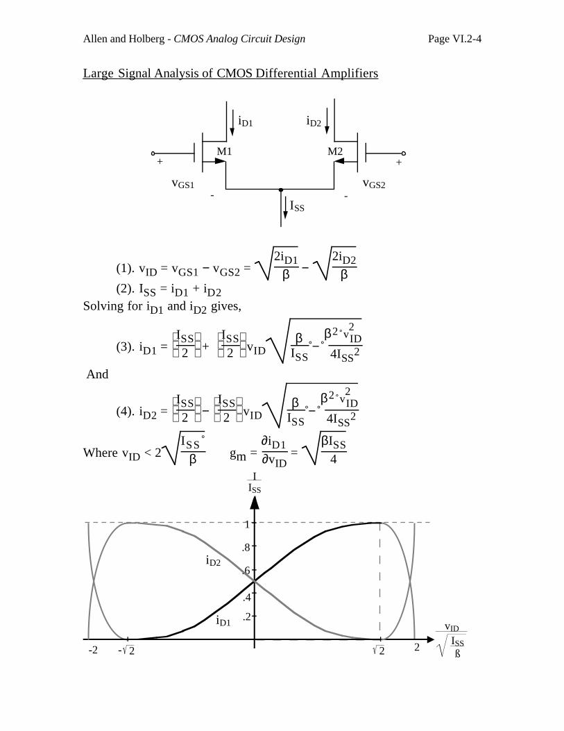
Allen and Holberg - CMOS Analog Circuit Design Page VI.2-4
Large Signal Analysis of CMOS Differential Amplifiers
ISS
M1 M2+
-
+
-vGS1 vGS2
iD1 iD2
(1). vID = vGS1 − vGS2 = 2iD1
β − 2iD2
β(2). ISS = iD1 + iD2
Solving for iD1 and iD2 gives,
(3). iD1 =
ISS
2 +
ISS
2 vIDβ
ISS −
β2 v2ID
4ISS2
And
(4). iD2 =
ISS
2 −
ISS
2 vIDβ
ISS −
β2 v2ID
4ISS2
Where vID < 2ISS
β gm = ∂iD1∂vID
= βISS
4
.2
22
.4
.6
.8
1
2-2
iD1
iD2
-
IISS
vID
ISSß
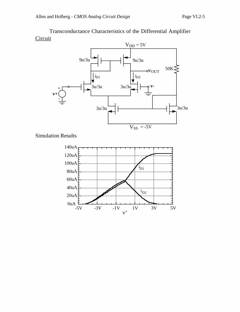
Allen and Holberg - CMOS Analog Circuit Design Page VI.2-5
Transconductance Characteristics of the Differential Amplifier Circuit
vOUT
v-
v+
9u/3u 9u/3u
3u/3u 3u/3u
3u/3u 3u/3u
+
-
50K
VDD = 5V
VSS = -5V
iD1 iD2
Simulation Results
0uA
20uA
40uA
60uA
80uA
100uA
120uA
140uA
-5V -3V -1V 1V 3V 5V
iD1
iD2
v+
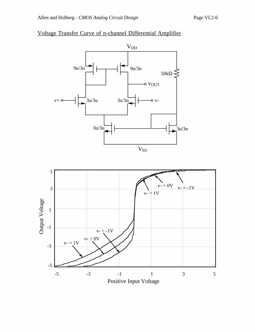
Allen and Holberg - CMOS Analog Circuit Design Page VI.2-6
Voltage Transfer Curve of n-channel Differential Amplifier
VSS
vOUT
v-v+
VDD
9u/3u 9u/3u
3u/3u 3u/3u
3u/3u 3u/3u
50kΩ
-5
-3
-1
1
3
5
-5 -3 -1 1 3 5
Positive Input Voltage
Out
put V
olta
ge
v- = -1V
v- = 0Vv- = 1V
v- = -1Vv- = 0V
v- = 1V
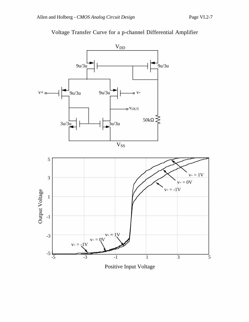
Allen and Holberg - CMOS Analog Circuit Design Page VI.2-7
Voltage Transfer Curve for a p-channel Differential Amplifier
v-v+ 9u/3u 9u/3u
3u/3u 3u/3u
VSS
VDD
9u/3u 9u/3u
vOUT
50kΩ
-5
-3
-1
1
3
5
-5 -3 -1 1 3 5
Positive Input Voltage
Out
put V
olta
ge
v- = 1V
v- = 0V
v- = -1V
v- = 1Vv- = 0V
v- = -1V
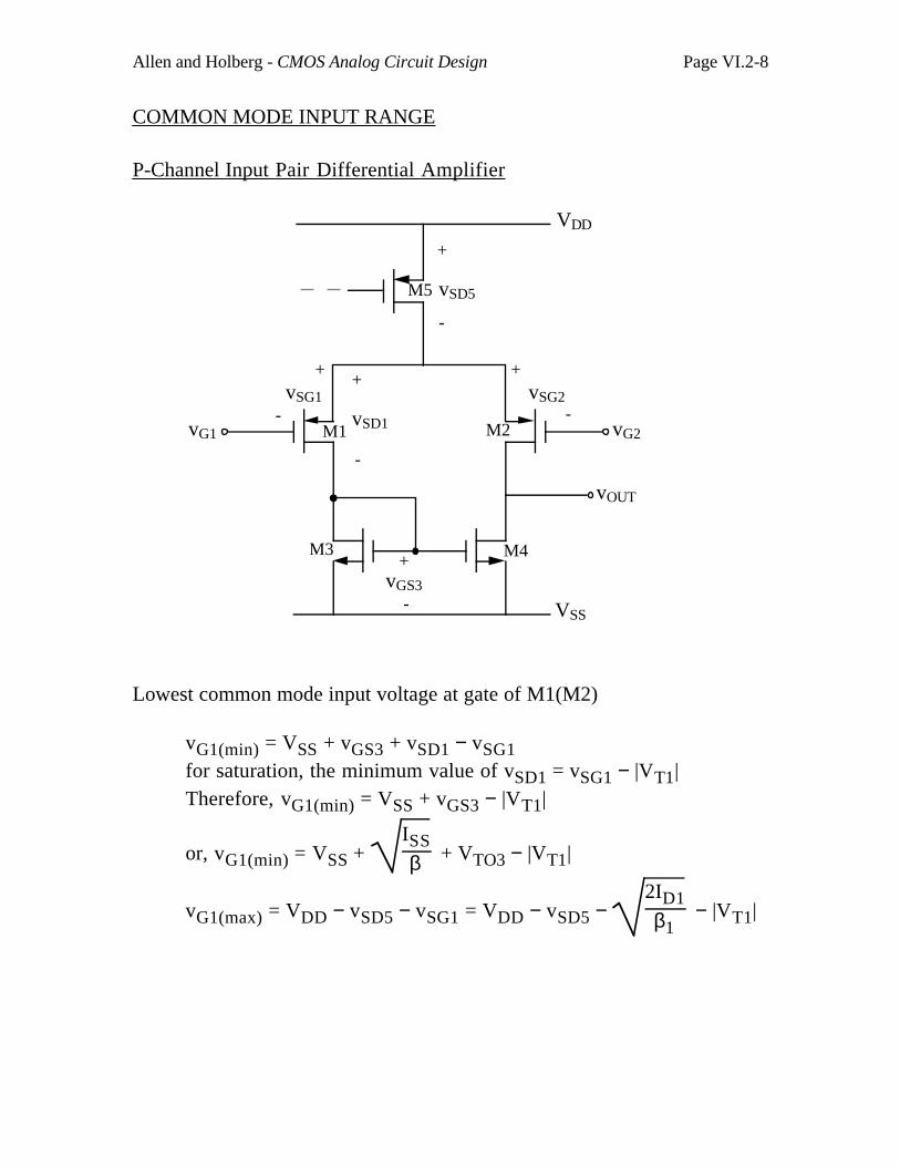
Allen and Holberg - CMOS Analog Circuit Design Page VI.2-8
COMMON MODE INPUT RANGE
P-Channel Input Pair Differential Amplifier
M4M3
M2M1
VDD
VSS
vG1 vG2
vOUT
+
-
+
-
M5
+
-
vSD5
vSG1 vSG2
+
-
+
-
vSD1
vGS3
Lowest common mode input voltage at gate of M1(M2)
vG1(min) = VSS + vGS3 + vSD1 − vSG1for saturation, the minimum value of vSD1 = vSG1 − |VT1|Therefore, vG1(min) = VSS + vGS3 − |VT1|
or, vG1(min) = VSS + ISSβ + VTO3 − |VT1|
vG1(max) = VDD − vSD5 − vSG1 = VDD − vSD5 − 2ID1β1
− |VT1|
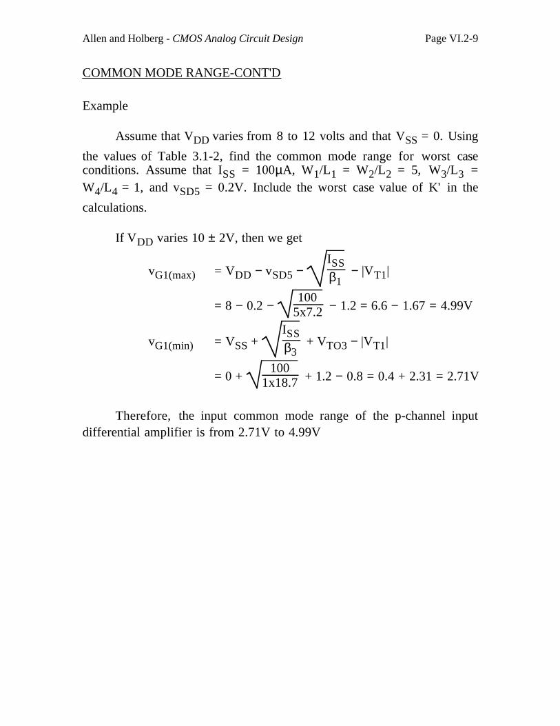
Allen and Holberg - CMOS Analog Circuit Design Page VI.2-9
COMMON MODE RANGE-CONT'D
Example
Assume that VDD varies from 8 to 12 volts and that VSS = 0. Using
the values of Table 3.1-2, find the common mode range for worst caseconditions. Assume that ISS = 100µA, W1/L1 = W2/L2 = 5, W3/L3 =W4/L4 = 1, and vSD5 = 0.2V. Include the worst case value of K' in the
calculations.
If VDD varies 10 ± 2V, then we get
vG1(max) = VDD − vSD5 − ISSβ1
− |VT1|
= 8 − 0.2 − 100
5x7.2 − 1.2 = 6.6 − 1.67 = 4.99V
vG1(min) = VSS + ISSβ3
+ VTO3 − |VT1|
= 0 + 100
1x18.7 + 1.2 − 0.8 = 0.4 + 2.31 = 2.71V
Therefore, the input common mode range of the p-channel inputdifferential amplifier is from 2.71V to 4.99V
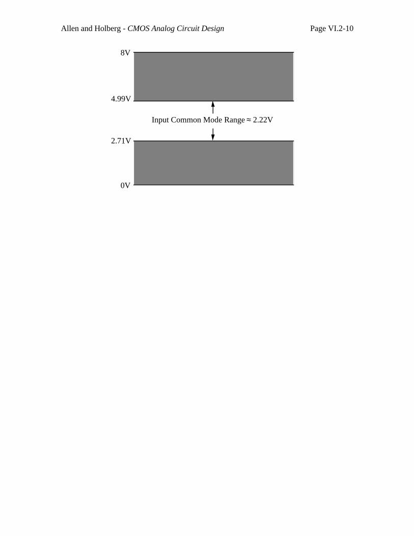
Allen and Holberg - CMOS Analog Circuit Design Page VI.2-10
Input Common Mode Range
8V
4.99V
2.71V
0V
≈ 2.22V
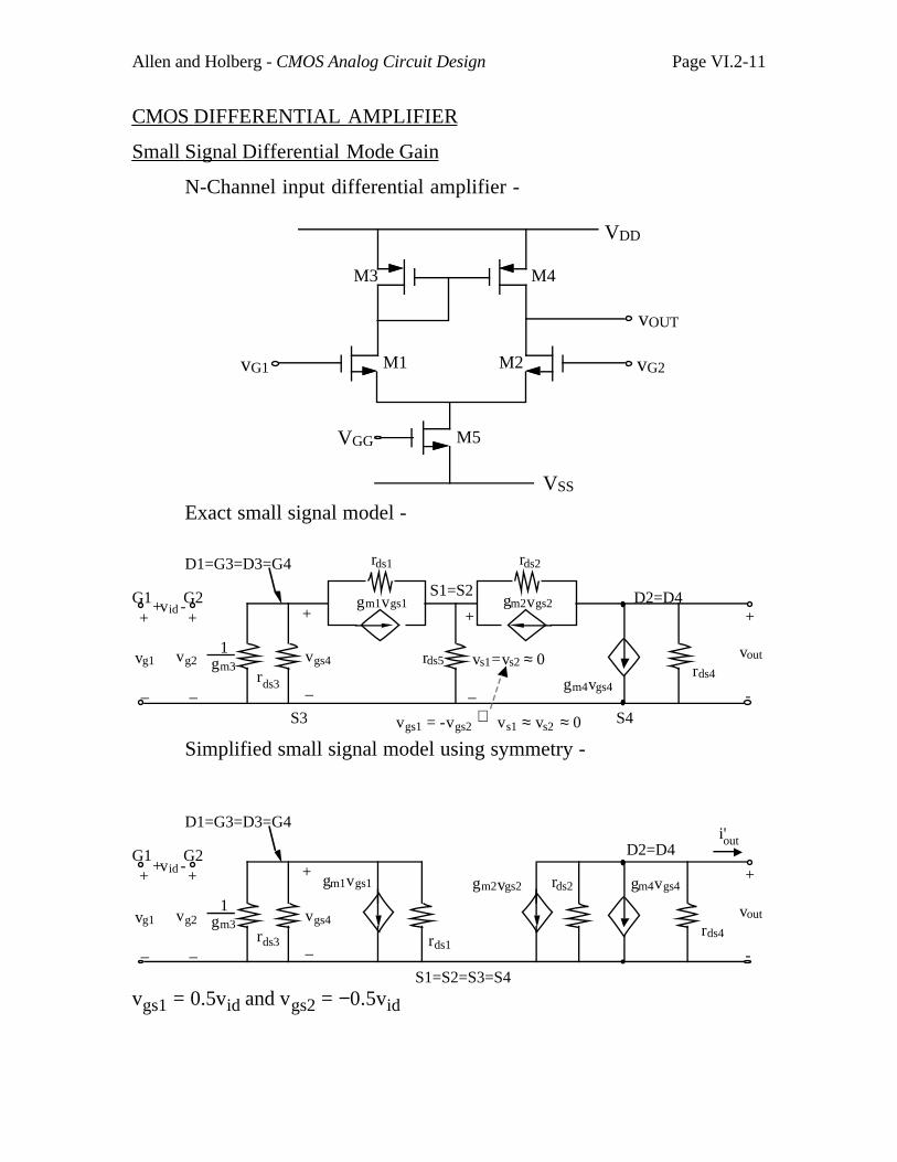
Allen and Holberg - CMOS Analog Circuit Design Page VI.2-11
CMOS DIFFERENTIAL AMPLIFIER
Small Signal Differential Mode Gain
N-Channel input differential amplifier -
M2 vG2
VDD
VSS
vOUT
M1
M3 M4
vG1
VGG M5
Exact small signal model -
D2=D4
S4
rds4
rds2
S1=S2
rds5
+
_
rds1
rds3
D1=G3=D3=G4
S3
gm1vgs1 gm2vgs2
vs1=vs21
gm3
G1 G2+
_
vg1
+ -vid +
-
vout≈ 0
vgs1 = -vgs2 ⇒ vs1 ≈ vs2 ≈ 0
gm4vgs4
+
_
vg2 vgs4
+
_
Simplified small signal model using symmetry -
D2=D4
rds4
rds2
rds1rds3
D1=G3=D3=G4
S1=S2=S3=S4
gm1vgs1 gm2vgs2
1gm3
G1 G2+
_
vg1
+ -vid +
-
vout
gm4vgs4+
_
vg2 vgs4
+
_
i'out
vgs1 = 0.5vid and vgs2 = −0.5vid
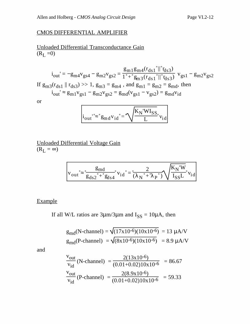
Allen and Holberg - CMOS Analog Circuit Design Page VI.2-12
CMOS DIFFERENTIAL AMPLIFIER
Unloaded Differential Transconductance Gain(RL =0)
iout' = −gm4vgs4 − gm2vgs2 = gm1gm4(rds1 || rds3)
1 + gm3(rds1 || rds3) vgs1 − gm2vgs2
If gm3(rds1 || rds3) >> 1, gm3 = gm4 , and gm1 = gm2 = gmd, theniout' ≈ gm1vgs1 − gm2vgs2 = gmd(vgs1 − vgs2) = gmdvid
or
iout' ≈ gmdvid = KN'WISS
L vid
Unloaded Differential Voltage Gain(RL = ∞)
vout ≈ gmd
gds2 + gds4 v id =
2(λ N + λ P )
KN'W
ISSL vid
Example
If all W/L ratios are 3µm/3µm and ISS = 10µA, then
gmd(N-channel) = (17x10-6)(10x10-6) = 13 µA/V
gmd(P-channel) = (8x10⁻⁶)(10x10-6) = 8.9 µA/V
andvoutvid
(N-channel) = 2(13x10-6)
(0.01+0.02)10x10-6 = 86.67
voutvid
(P-channel) = 2(8.9x10⁻⁶)
(0.01+0.02)10x10-6 = 59.33
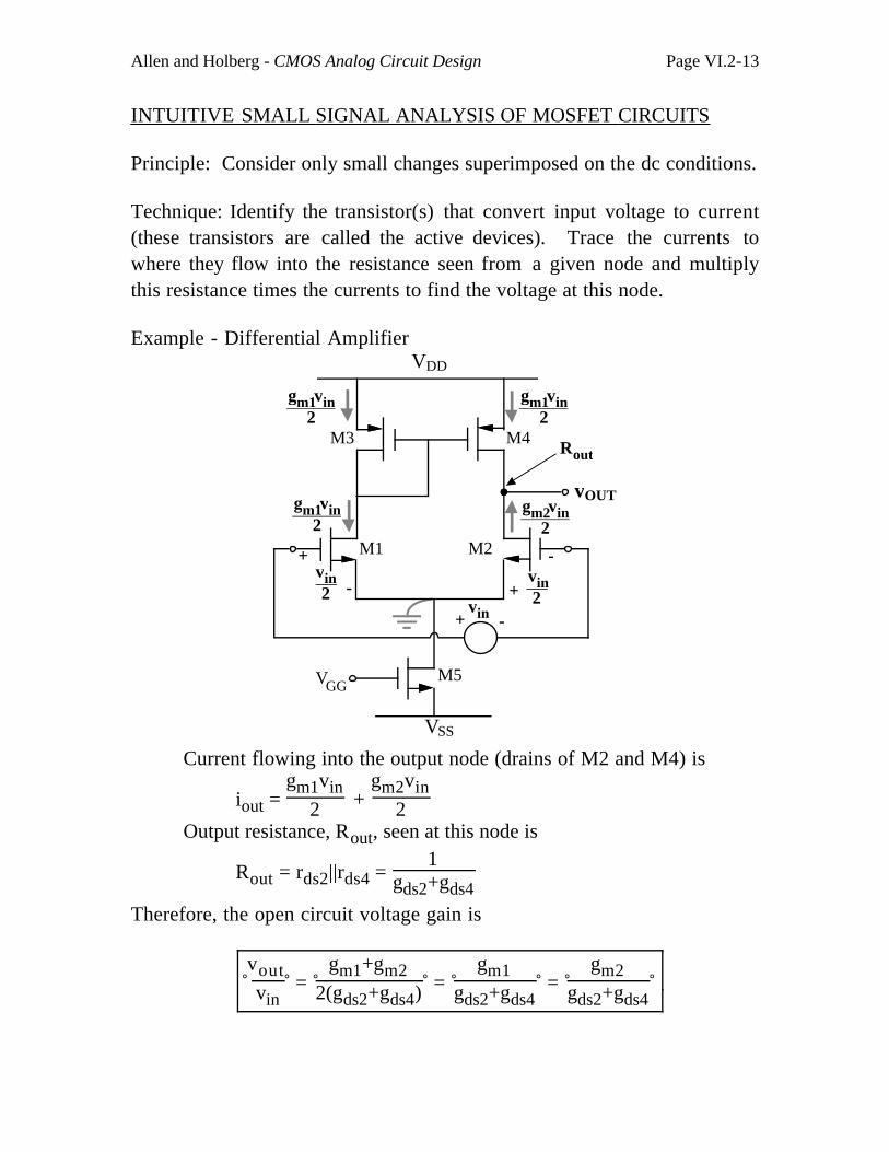
Allen and Holberg - CMOS Analog Circuit Design Page VI.2-13
INTUITIVE SMALL SIGNAL ANALYSIS OF MOSFET CIRCUITS
Principle: Consider only small changes superimposed on the dc conditions.
Technique: Identify the transistor(s) that convert input voltage to current(these transistors are called the active devices). Trace the currents towhere they flow into the resistance seen from a given node and multiplythis resistance times the currents to find the voltage at this node.
Example - Differential Amplifier
vOUT
VSS
VDD
M3 M4
M1 M2
M5VGG
+ -vin
vin2
vin2 +
-+
-
gm1vin2
gm1vin2
gm1vin2
gm2vin2
Rout
Current flowing into the output node (drains of M2 and M4) is
iout = gm1vin
2 + gm2vin
2
Output resistance, Rout, seen at this node is
Rout = rds2||rds4 = 1
gds2+gds4
Therefore, the open circuit voltage gain is
voutvin
= gm1+gm2
2(gds2+gds4) = gm1
gds2+gds4 =
gm2gds2+gds4
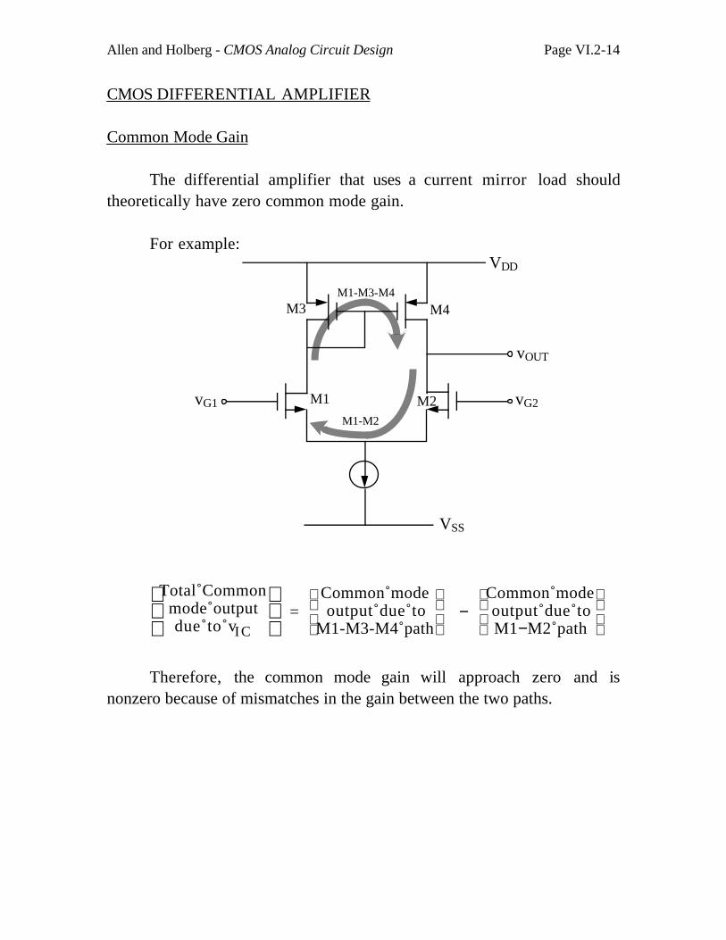
Allen and Holberg - CMOS Analog Circuit Design Page VI.2-14
CMOS DIFFERENTIAL AMPLIFIER
Common Mode Gain
The differential amplifier that uses a current mirror load shouldtheoretically have zero common mode gain.
For example:
M2 vG2
VDD
VSS
vOUT
M1
M3 M4
vG1
M1-M3-M4
M1-M2
Total Common
mode outputdue to vIC
=
Common mode
output due toM1-M3-M4 path
−
Common mode
output due toM1−M2 path
Therefore, the common mode gain will approach zero and isnonzero because of mismatches in the gain between the two paths.
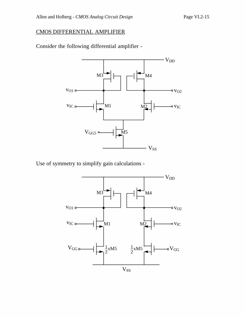
Allen and Holberg - CMOS Analog Circuit Design Page VI.2-15
CMOS DIFFERENTIAL AMPLIFIER
Consider the following differential amplifier -
M2
VDD
VSS
M1
M3 M4
M5
vO1 vO2
vICvIC
VGG5
Use of symmetry to simplify gain calculations -
M2
VDD
VSS
M1
M3 M4
vO1 vO2
vICvIC
VGGVGG 12
xM5 12
xM5
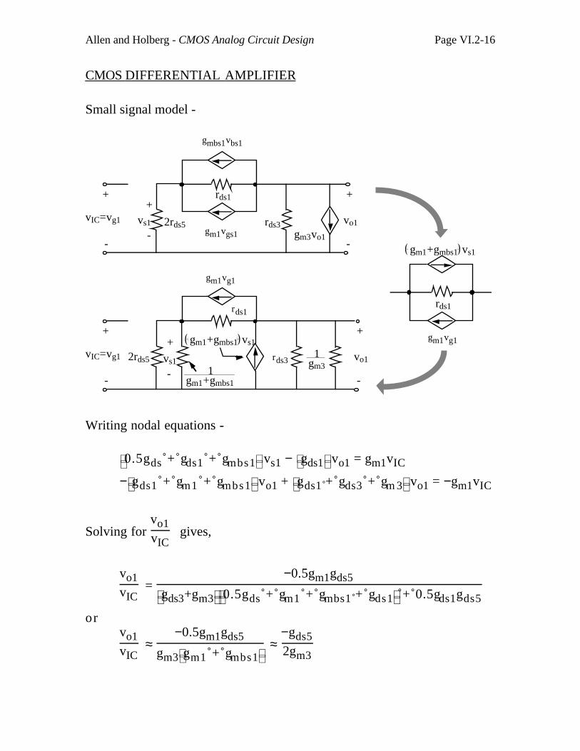
Allen and Holberg - CMOS Analog Circuit Design Page VI.2-16
CMOS DIFFERENTIAL AMPLIFIER
Small signal model -
+
-
vIC=vg1
+
-vs1 2rds5
rds1
rds3gm3vo1
+
-
vo1
+
-
vIC=vg1
+
-vs12rds5
+
-
vo11gm31
gm1+gmbs1
gm1+gmbs1 vs1
rds1
gm1+gmbs1 vs1
gm1vg1
gm1vgs1
gmbs1vbs1
rds1
rds3
gm1vg1
Writing nodal equations -
0.5gds + gds1 + gmbs1 vs1 − gds1 vo1 = gm1vIC
− gds1 + gm1 + gmbs1 vo1 + gds1 + gds3 + gm 3 vo1 = −gm1vIC
Solving for vo1vIC
gives,
vo1vIC
= −0.5gm1gds5
gds3+gm3 0.5gds + gm1 + gmbs1 + gds1 + 0.5gds1gds5
orvo1vIC
≈ −0.5gm1gds5
gm3 gm1 + gmbs1 ≈
−gds52gm3
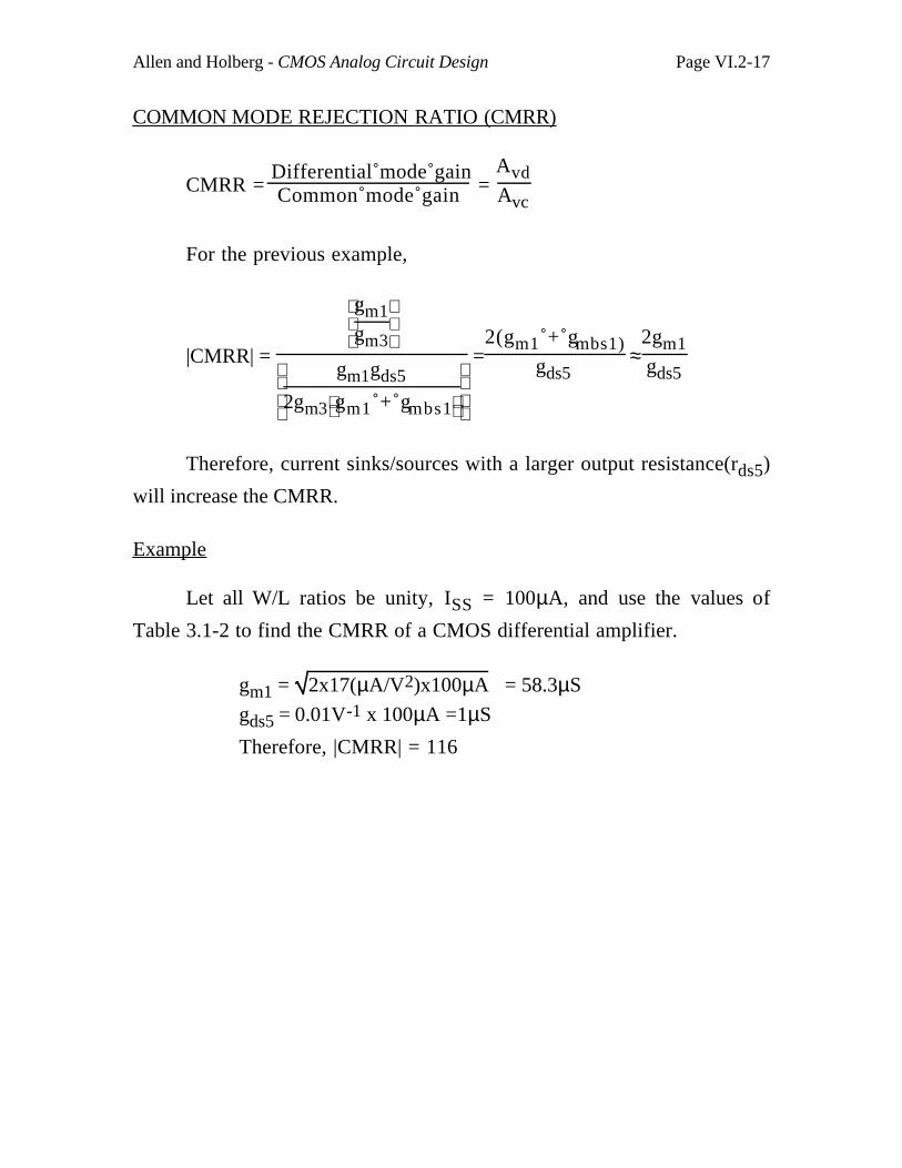
Allen and Holberg - CMOS Analog Circuit Design Page VI.2-17
COMMON MODE REJECTION RATIO (CMRR)
CMRR = Differential mode gainCommon mode gain =
AvdAvc
For the previous example,
|CMRR| =
gm1
gm3
gm1gds5
2gm3 gm1 + gmbs1
=2(gm1 + gmbs1)
gds5 ≈
2gm1gds5
Therefore, current sinks/sources with a larger output resistance(rds5)
will increase the CMRR.
Example
Let all W/L ratios be unity, ISS = 100µA, and use the values of
Table 3.1-2 to find the CMRR of a CMOS differential amplifier.
gm1 = 2x17(µA/V2)x100µA = 58.3µS
gds5 = 0.01V-1 x 100µA =1µS
Therefore, |CMRR| = 116
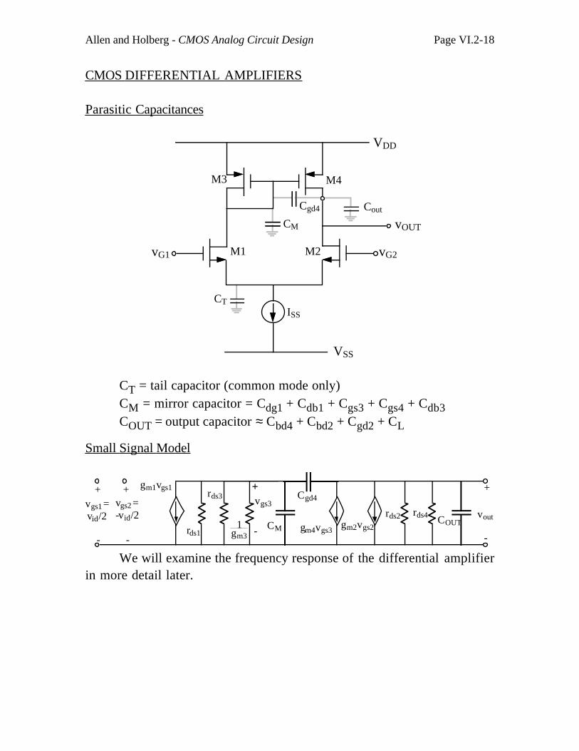
Allen and Holberg - CMOS Analog Circuit Design Page VI.2-18
CMOS DIFFERENTIAL AMPLIFIERS
Parasitic Capacitances
M2 vG2
VDD
VSS
vOUT
M1
M3 M4
vG1
Cout
CM
CTISS
Cgd4
CT = tail capacitor (common mode only)CM = mirror capacitor = Cdg1 + Cdb1 + Cgs3 + Cgs4 + Cdb3COUT = output capacitor ≈ Cbd4 + Cbd2 + Cgd2 + CL
Small Signal Model
CMCOUT
Cgd4
gm1vgs1
gm2vgs2
vout
rds1
rds3
1gm3
rds2 rds4
+
-
vgs2 =-vid/2
vgs1 =vid/2
+
-
+
-gm4vgs3
vgs3
+
-
We will examine the frequency response of the differential amplifierin more detail later.
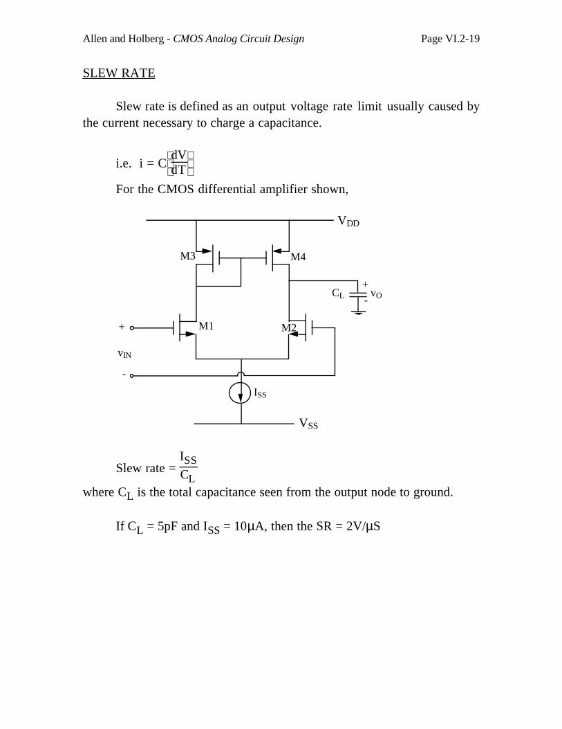
Allen and Holberg - CMOS Analog Circuit Design Page VI.2-19
SLEW RATE
Slew rate is defined as an output voltage rate limit usually caused bythe current necessary to charge a capacitance.
i.e. i = C
dV
dT
For the CMOS differential amplifier shown,
M2
VDD
VSS
M1
M3 M4
ISS
CL+
-vO
+
-
vIN
Slew rate = ISSCL
where CL is the total capacitance seen from the output node to ground.
If CL = 5pF and ISS = 10µA, then the SR = 2V/µS
Allen and Holberg - CMOS Analog Circuit Design Page VI.2-20
CMOS DIFFERENTIAL AMPLIFIERS
NOISE
Assumption:
Neglect thermal noise(low frequency) and ignore the thermal noisesources of rd and rs .
Therefore:
i2nd =
KF
fCoxL2 iDAF (AF = 0.8 and KF = 10-28)
or
v2nd =
i2nd
gm2 =
KF
2fµoCox2WL
iD(AF-1)
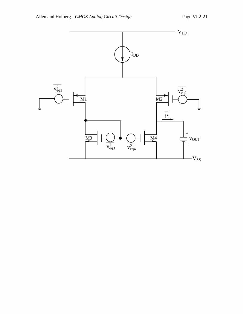
Allen and Holberg - CMOS Analog Circuit Design Page VI.2-21
VDD
IDD
VSS
vOUTM4M3
M2M1
veq32 veq4
2
veq22
+
-
veq12
io2
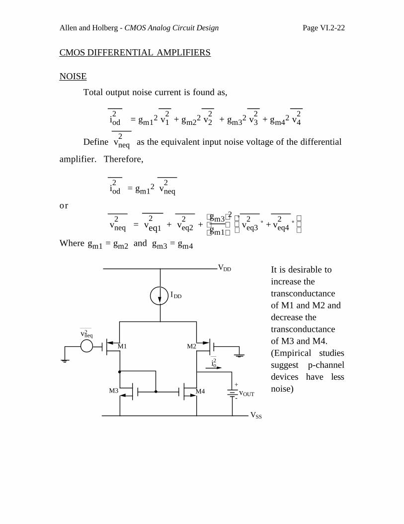
Allen and Holberg - CMOS Analog Circuit Design Page VI.2-22
CMOS DIFFERENTIAL AMPLIFIERS
NOISE
Total output noise current is found as,
i2od = gm1
2 v21
+ gm22 v
22 + gm3
2 v23
+ gm42 v
24
Define v2neq
as the equivalent input noise voltage of the differential
amplifier. Therefore,
i2od = gm1
2 v2neq
or
v2neq = v
2eq1 + v
2eq2 +
gm3
gm1
2
v2eq3 + v
2eq4
Where gm1 = gm2 and gm3 = gm4
M4M3
M2M1
VDD
IDD
VSS
vOUT
vneq2
io2
+
-
It is desirable toincrease thetransconductanceof M1 and M2 anddecrease thetransconductanceof M3 and M4.(Empirical studiessuggest p-channeldevices have lessnoise)
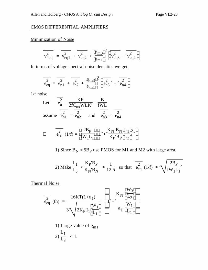
Allen and Holberg - CMOS Analog Circuit Design Page VI.2-23
CMOS DIFFERENTIAL AMPLIFIERS
Minimization of Noise
v2neq = v
2eq1 + v
2eq2 +
gm3
gm1
2
v2eq3 + v
2eq4
In terms of voltage spectral-noise densities we get,
e2eq = e
2n1 + e
2n2 +
gm3
gm1
2
e2n3 + e
2n4
1/f noise
Let e2n =
KF2fCoxWLK' =
BfWL
assume e2n1 = e
2n2 and e
2n3 = e
2n4
∴ e2eq (1/f) =
2BP
fW1L1
1 + KN'BNKP'BP
L1
L3
2
1) Since BN ≈ 5BP use PMOS for M1 and M2 with large area.
2) Make L1L3
< KP'BPKN'BN
≈ 1
12.5 so that e2eq (1/f) ≈
2BPfW1L1
Thermal Noise
e2eq (th) =
16KT(1+η1)
3 2KP'I1
W1
L1
1 +
K N '
W3
L3
KP'
W1
L1
1) Large value of gm1.
2) L1L3
< 1.
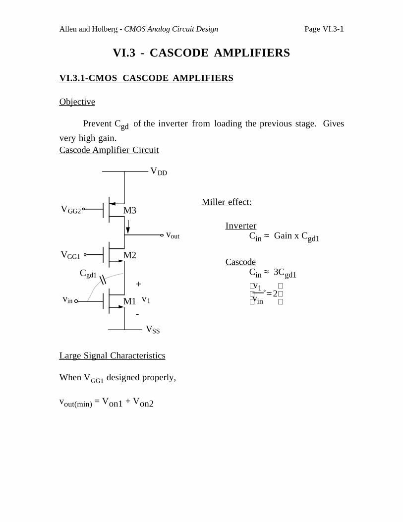
Allen and Holberg - CMOS Analog Circuit Design Page VI.3-1
VI.3 - CASCODE AMPLIFIERS
VI.3.1-CMOS CASCODE AMPLIFIERS
Objective
Prevent Cgd of the inverter from loading the previous stage. Gives
very high gain. Cascode Amplifier Circuit
Large Signal Characteristics
When VGG1 designed properly,
vout(min) = Von1 + Von2
vout
VSS
VDD
M3
M2
M1
+
-
Cgd1
vin
VGG1
VGG2
v1
Miller effect:
Inverter Cin ≈ Gain x Cgd1
Cascode Cin ≈ 3Cgd1
v1
vin ≈ 2
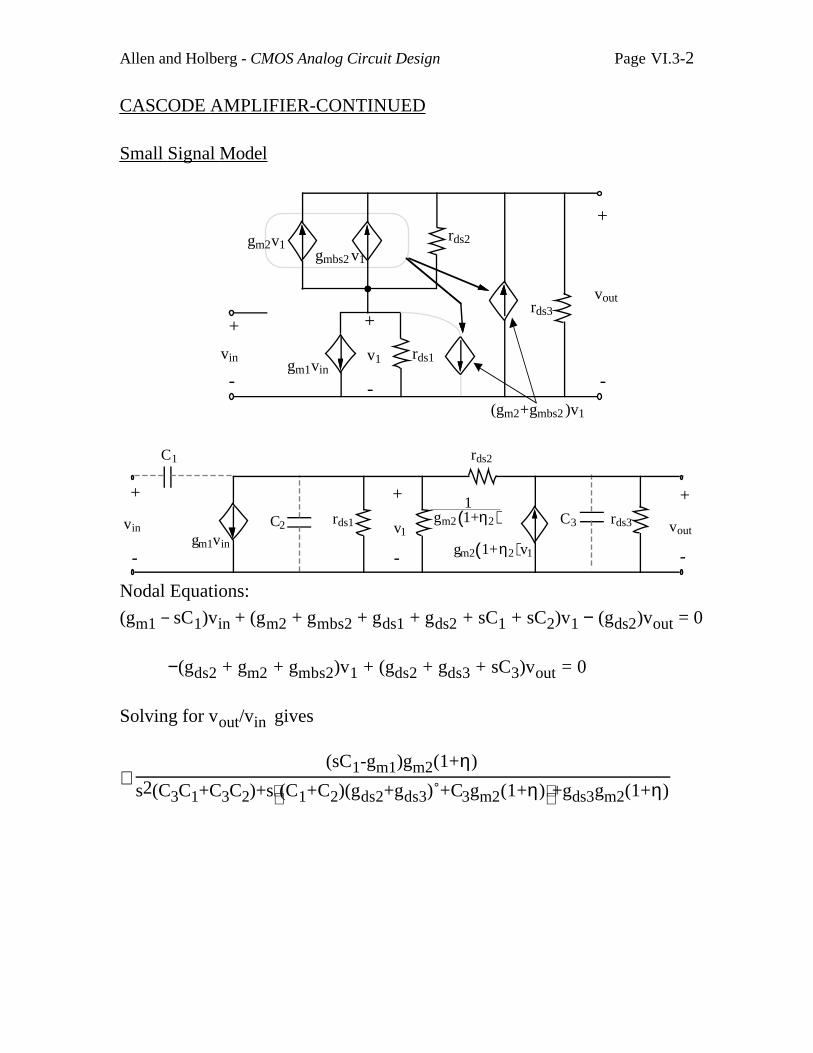
Allen and Holberg - CMOS Analog Circuit Design Page VI.3-2
CASCODE AMPLIFIER-CONTINUED
Small Signal Model
+
-
gm2v1gmbs2 v1
gm1vinvin
+
-
v1 rds1
rds2
rds3
+
-
vout
(gm2+gmbs2 )v1
rds2
+
-
v1rds1 vout
+
-gm1vin
+
-
vin
C1
C2 C3 rds3
1gm2( )1+η2
gm2( )1+η2 v1
Nodal Equations:
(gm1 − sC1)vin + (gm2 + gmbs2 + gds1 + gds2 + sC1 + sC2)v1 − (gds2)vout = 0
−(gds2 + gm2 + gmbs2)v1 + (gds2 + gds3 + sC3)vout = 0
Solving for vout/vin gives
≅ (sC1-gm1)gm2(1+η)
s2(C3C1+C3C2)+s (C1+C2)(gds2+gds3) +C3gm2(1+η) +gds3gm2(1+η)
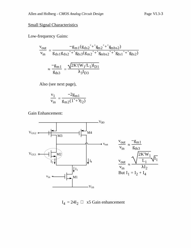
Allen and Holberg - CMOS Analog Circuit Design Page VI.3-3
Small Signal Characteristics
Low-frequency Gains:
voutvin
= −gm1(gds2 + gm2 + gmbs2)
gds1gds2 + gds3(gm2 + gmbs2 + gds1 + gds2)
≈ −gm1gds3
= 2K'(W1/L1)ID1
λ3ID3
Also (see next page),
v1vin
= −2gm1
gm2(1 + η2)
Gain Enhancement:
M1vin
VDD
VSS
VGG2
VGG1 M2
M4M3
I4
I1
I2
voutvoutvin
≈ −gm1gds3
voutvin
≈
2K'W1L1
I1
λI2
But I1 = I2 + I4
I4 = 24I2 ⇒ x5 Gain enhancement
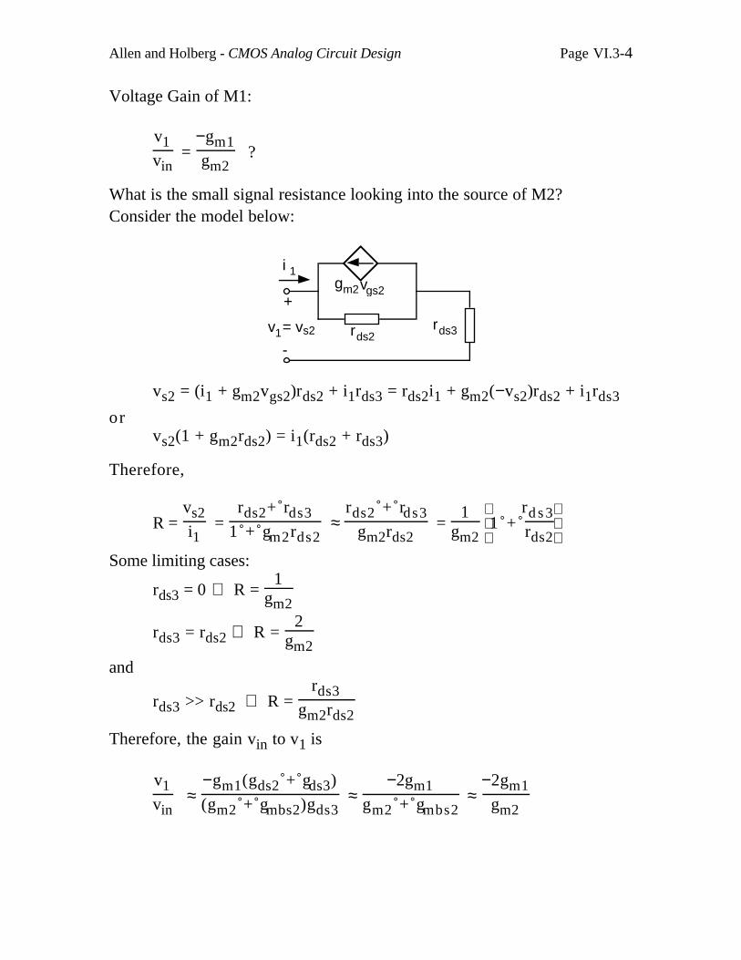
Allen and Holberg - CMOS Analog Circuit Design Page VI.3-4
Voltage Gain of M1:
v1vin
= −gm1gm2
?
What is the small signal resistance looking into the source of M2?Consider the model below:
rds2
+
-
v1
i 1gm2vgs2
= vs2 rds3
vs2 = (i1 + gm2vgs2)rds2 + i1rds3 = rds2i1 + gm2(−vs2)rds2 + i1rds3
orvs2(1 + gm2rds2) = i1(rds2 + rds3)
Therefore,
R = vs2i1
= rds2+ rds3
1 + gm2rds2 ≈
rds2 + rds3gm2rds2
= 1
gm2
1 + rd s 3rds2
Some limiting cases:
rds3 = 0 ⇒ R = 1
gm2
rds3 = rds2 ⇒ R = 2
gm2
and
rds3 >> rds2 ⇒ R = rds3
gm2rds2
Therefore, the gain vin to v1 is
v1vin
≈ −gm1(gds2 + gds3)
(gm2 + gmbs2)gds3 ≈
−2gm1gm2 + gmbs2
≈ −2gm1
gm2
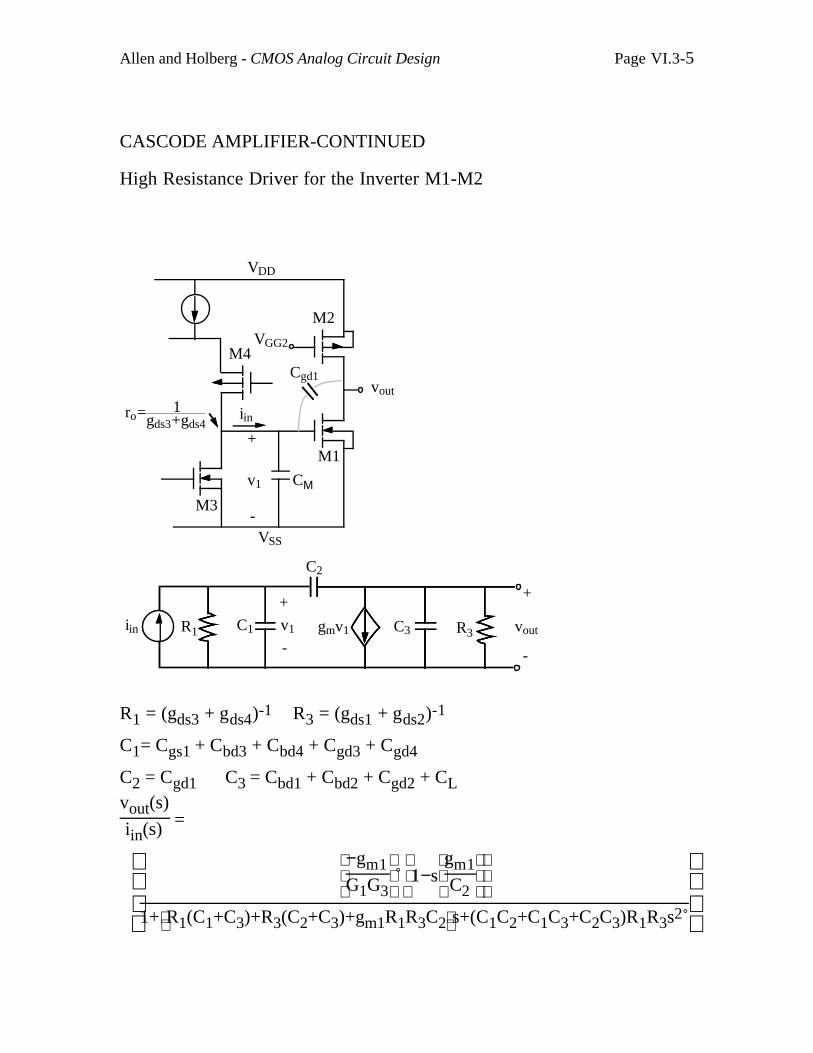
Allen and Holberg - CMOS Analog Circuit Design Page VI.3-5
M3
M1
M4
M2
+
-
CΜv1
vout
VDD
VGG2
Cgd1
iin
VSS
ro= 1gds3+gds4
iin C3
C2
C1
+
-
v1 gmv1
+
-
voutR1 R3
R1 = (gds3 + gds4)-1 R3 = (gds1 + gds2)-1
C1= Cgs1 + Cbd3 + Cbd4 + Cgd3 + Cgd4
C2 = Cgd1 C3 = Cbd1 + Cbd2 + Cgd2 + CLvout(s)
iin(s) =
−gm1
G1G3
1−s
gm1
C2
1+ R1(C1+C3)+R3(C2+C3)+gm1R1R3C2 s+(C1C2+C1C3+C2C3)R1R3s2
CASCODE AMPLIFIER-CONTINUED
High Resistance Driver for the Inverter M1-M2
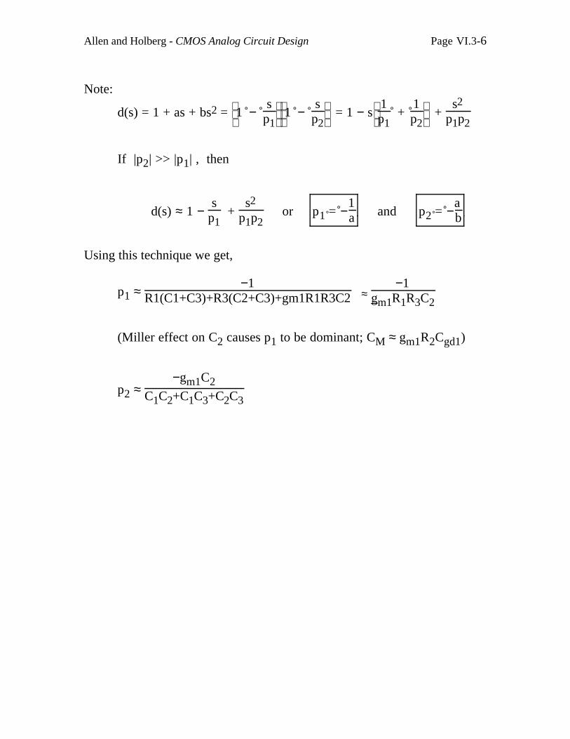
Allen and Holberg - CMOS Analog Circuit Design Page VI.3-6
Note:
d(s) = 1 + as + bs2 =
1 −
sp1
1 −
sp2
= 1 − s
1
p1 +
1p2
+ s2
p1p2
If |p2| >> |p1| , then
d(s) ≈ 1 − s
p1 +
s2
p1p2 or p1 = −1
a and p2 = −ab
Using this technique we get,
p1 ≈ −1
R1(C1+C3)+R3(C2+C3)+gm1R1R3C2 ≈ −1
g m1R1R3C2
(Miller effect on C2 causes p1 to be dominant; CM ≈ gm1R2Cgd1)
p2 ≈ −gm1C2
C1C2+C1C3+C2C3
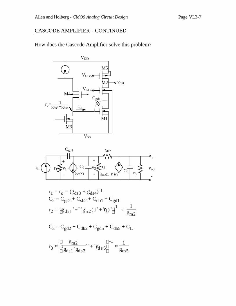
Allen and Holberg - CMOS Analog Circuit Design Page VI.3-7
CASCODE AMPLIFIER - CONTINUED
How does the Cascode Amplifier solve this problem?
M3
M4
VDD
M2VGG2
M1
Cgd1
iin
VSS
M5
VGG5
vout
ro= 1gds3+gds4
iinC3
C2
+
-
v1gmv1
+
-
vout
+
-
v2
rds2
gm2(1+η)v2
Cgd1
r1r2
r3
r1 = ro = (gds3 + gds4)-1
C2 = Cgs2 + Csb2 + Cdb1 + Cgd1
r2 = gds1 + gm 2(1 + η ) -1
≈ 1
gm2
C3 = Cgd2 + Cdb2 + Cgd5 + Cdb5 + CL
r3 ≈
gm2
gds1 gds2 + gd s 5
-1 ≈
1gds5
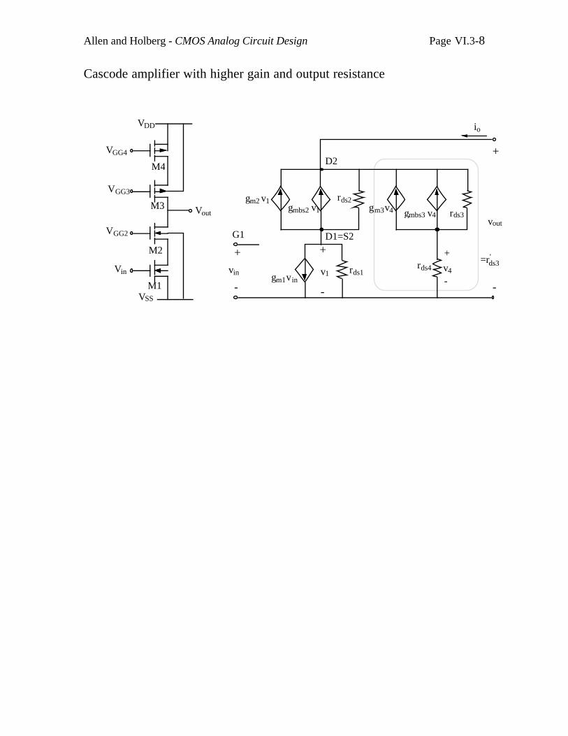
Allen and Holberg - CMOS Analog Circuit Design Page VI.3-8
Cascode amplifier with higher gain and output resistance
M3
M1
M4
M2
VGG2
VSS
VDD
Vin
Vout
VGG3
VGG4
gm2 v1gmbs2 v1
gm1vin
+
-
vin
+
-
v1 rds1
rds2
+
-
vout
D2
D1=S2G1
rds3
rds4
+
-v4
gmbs3 v4gm3v4
=rds3'
io
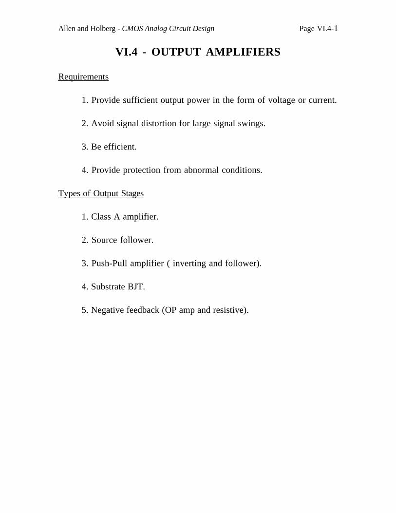
Allen and Holberg - CMOS Analog Circuit Design Page VI.4-1
VI.4 - OUTPUT AMPLIFIERS
Requirements
1. Provide sufficient output power in the form of voltage or current.
2. Avoid signal distortion for large signal swings.
3. Be efficient.
4. Provide protection from abnormal conditions.
Types of Output Stages
1. Class A amplifier.
2. Source follower.
3. Push-Pull amplifier ( inverting and follower).
4. Substrate BJT.
5. Negative feedback (OP amp and resistive).
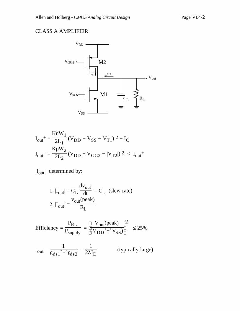
Allen and Holberg - CMOS Analog Circuit Design Page VI.4-2
CLASS A AMPLIFIER
M2
M1CL RL
VGG2
VSS
VDD
Vin
Vout
IQ Iout
Iout+ =
KnW12L1
(VDD − VSS − VT1) 2 − IQ
Iout - = KpW2
2L2 (VDD − VGG2 − |VT2|) 2 < Iout
+
|Iout| determined by:
1. |Iout| = CL dvout
dt = CL (slew rate)
2. |Iout| = vout(peak)
RL
Efficiency = PRL
Psupply =
Vout(peak)
(VDD + VSS)
2 ≤ 25%
rout = 1
gds1 + gds2 =
12λID
(typically large)
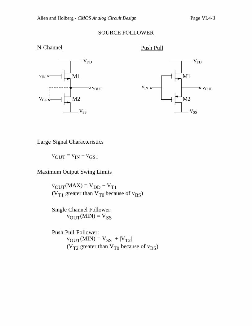
Allen and Holberg - CMOS Analog Circuit Design Page VI.4-3
SOURCE FOLLOWER
N-Channel
M1
M2VGG
vIN
vOUT
VDD
VSS
Large Signal Characteristics
vOUT = vIN − vGS1
Maximum Output Swing Limits
vOUT(MAX) = VDD − VT1(VT1 greater than VT0 because of vBS)
Single Channel Follower:vOUT(MIN) = VSS
Push Pull Follower:vOUT(MIN) = VSS + |VT2|(VT2 greater than VT0 because of vBS)
Push Pull
M1
M2
vOUT
VDD
VSS
vIN
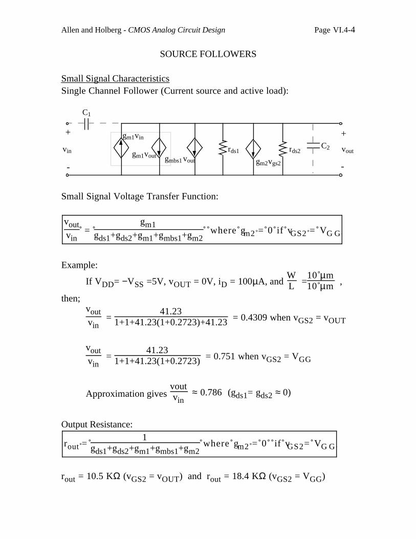
Allen and Holberg - CMOS Analog Circuit Design Page VI.4-4
SOURCE FOLLOWERS
Small Signal Characteristics Single Channel Follower (Current source and active load):
rds2 vout
+
-
gm1vin+
-
vin
C1
gm1vout gmbs1 vout gm2vgs2
rds1C2
Small Signal Voltage Transfer Function:
voutvin
= gm1
gds1+gds2+gm1+gmbs1+gm2 where gm2 = 0 if vGS2 = VG G
Example:
If VDD= −VSS =5V, vOUT = 0V, iD = 100µA, and WL =
10 µm10 µm ,
then;voutvin
= 41.23
1+1+41.23(1+0.2723)+41.23 = 0.4309 when vGS2 = vOUT
voutvin
= 41.23
1+1+41.23(1+0.2723) = 0.751 when vGS2 = VGG
Approximation gives voutvin
≈ 0.786 (gds1= gds2 ≈ 0)
Output Resistance:
rout = 1
gds1+gds2+gm1+gmbs1+gm2 where gm2 = 0 if vGS2= VG G
rout = 10.5 KΩ (vGS2 = vOUT) and rout = 18.4 KΩ (vGS2 = VGG)
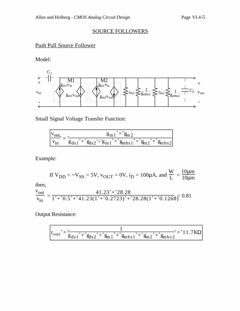
Allen and Holberg - CMOS Analog Circuit Design Page VI.4-5
SOURCE FOLLOWERS
Push Pull Source Follower
Model:
gm1vin+
-
vin
C1
gm1voutrds1 rds2 vout
+
-
C2
gm2vin
gm2vout
1gmbs1
1gmbs2
M1 M2
Small Signal Voltage Transfer Function:
voutvin
= gm1 + gm 2
gds1 + gds2 + gm1 + gmbs1 + gm2 + gmbs2
Example:
If VDD = −VSS = 5V, vOUT = 0V, iD = 100µA, and WL =
10µm10µm
then,voutvin
= 41.23 + 28.28
1 + 0.5 + 41.23(1 + 0.2723) + 28.28(1 + 0.1268) = 0.81
Output Resistance:
rout = 1
gds1 + gds2 + gm1 + gmbs1 + gm2 + gmbs2 = 11.7KΩ
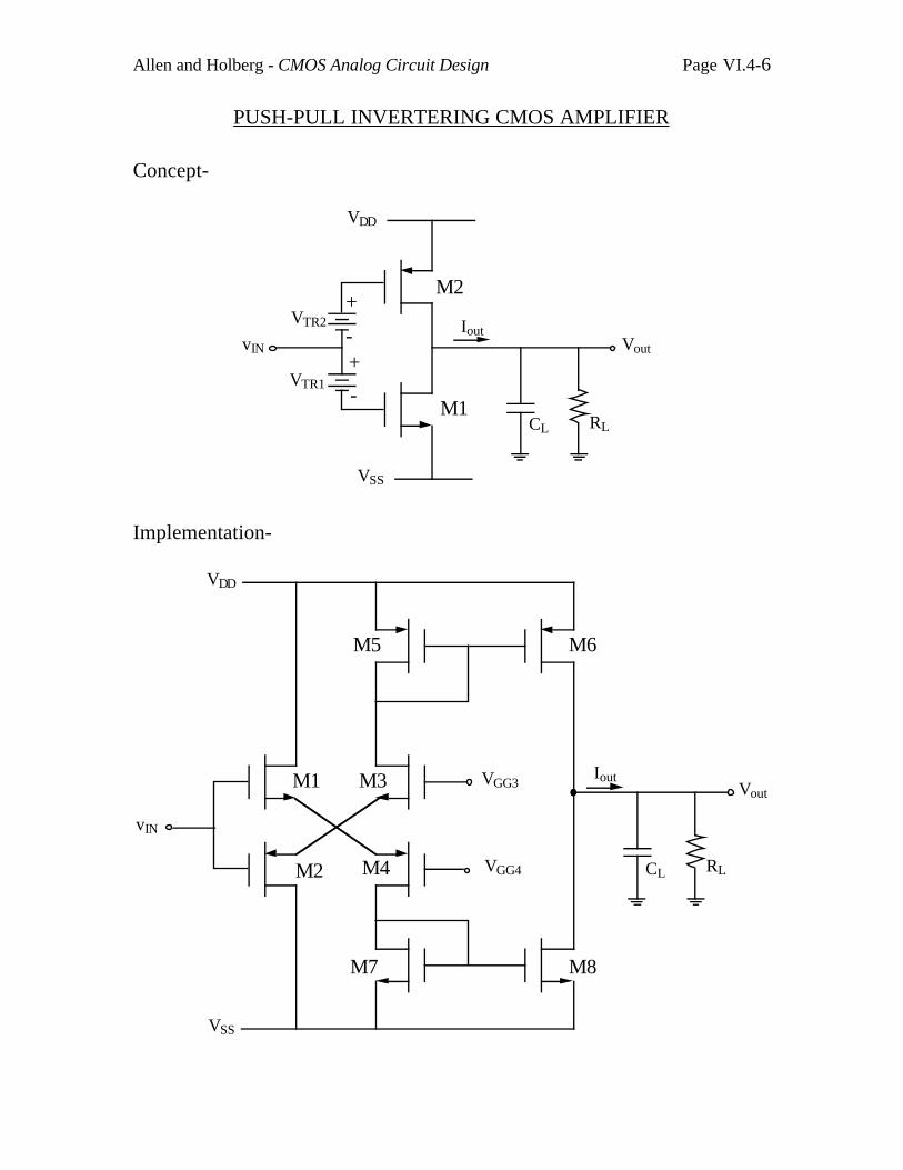
Allen and Holberg - CMOS Analog Circuit Design Page VI.4-6
PUSH-PULL INVERTERING CMOS AMPLIFIER
Concept-
M2
M1CL RL
VSS
VDD
Vout
Iout
VTR1
VTR2+
-+
-
vIN
Implementation-
VSS
VDD
Iout
vIN
M5 M6
M7 M8
M1
M2
M3
M4 CL RL
VoutVGG3
VGG4
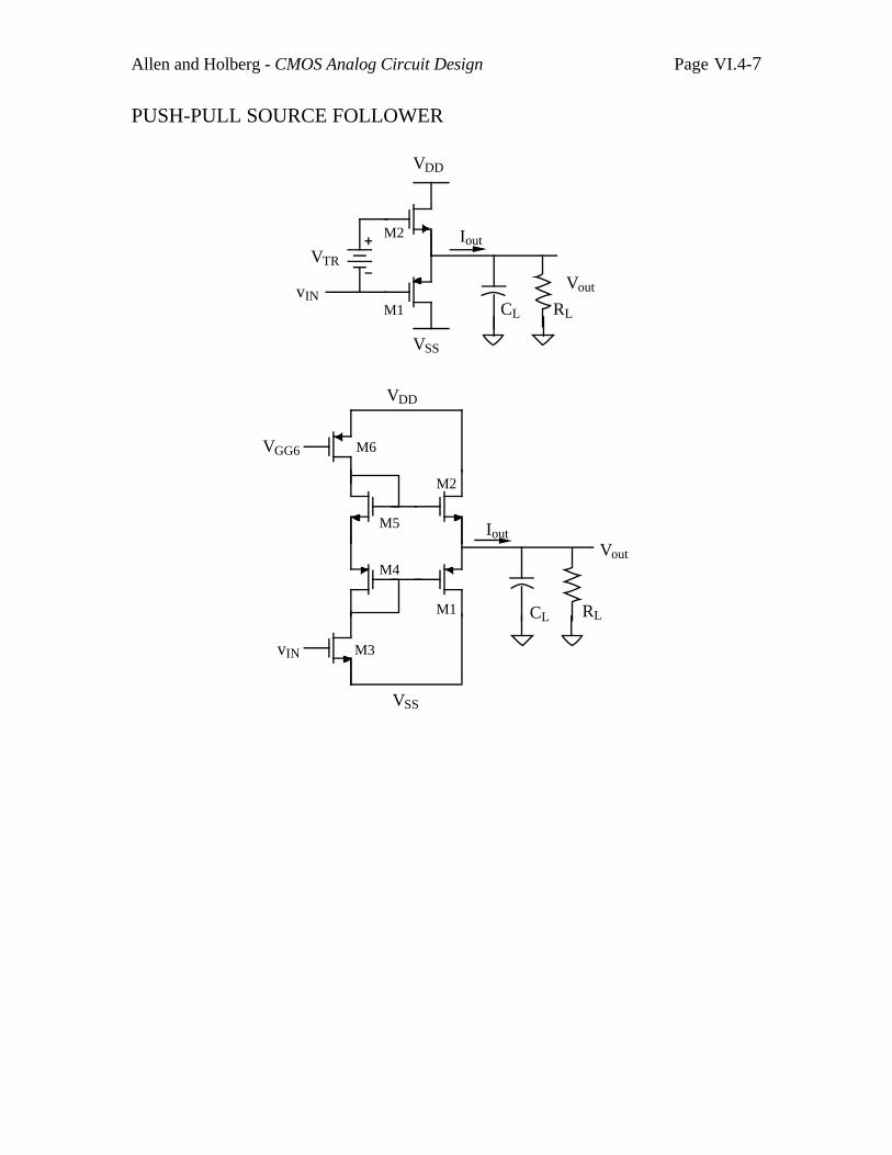
Allen and Holberg - CMOS Analog Circuit Design Page VI.4-7
PUSH-PULL SOURCE FOLLOWER
VSS
Vout
RLCL
VTR
vIN
VDD
M1
M2 Iout
M5
M4
M1
M2
M6
M3
VSS
VDD
VGG6
vIN
Iout
RLCL
Vout
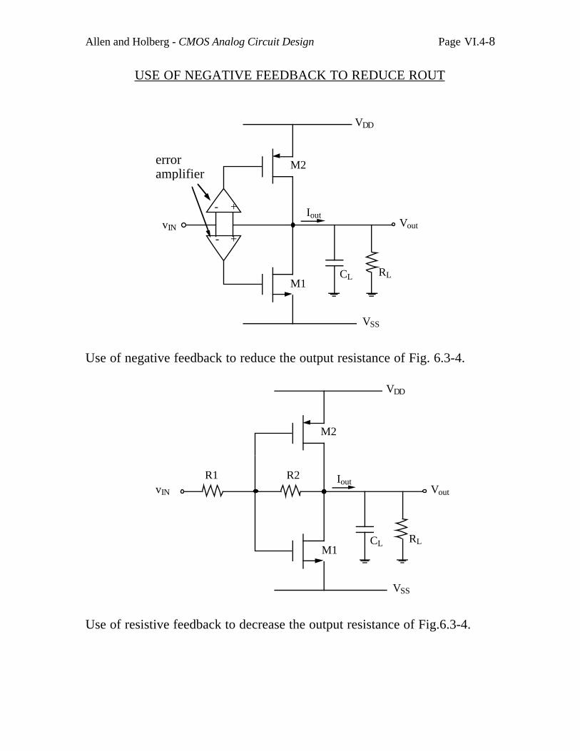
Allen and Holberg - CMOS Analog Circuit Design Page VI.4-8
USE OF NEGATIVE FEEDBACK TO REDUCE ROUT
Iout
CL RL
Vout
+
+
-
-
VDD
VSS
M2
M1
vIN
erroramplifier
Use of negative feedback to reduce the output resistance of Fig. 6.3-4.
Iout
CL RL
Vout
VDD
VSS
M2
M1
vIN
R2R1
Use of resistive feedback to decrease the output resistance of Fig.6.3-4.
Allen and Holberg - CMOS Analog Circuit Design Page VI.5-1
• Analog Amplifier Building Blocks
Inverters - Class APush-Pull - Class AB or BCascode - Increased bandwidthDifferential - Common mode rejection, good input stageOutput - Low output resistance with minimum distortion
VI.5 - SUMMARY
Allen and Holberg - CMOS Analog Circuit Design Page VII.0-1
SECTION 7 - COMPARATORS
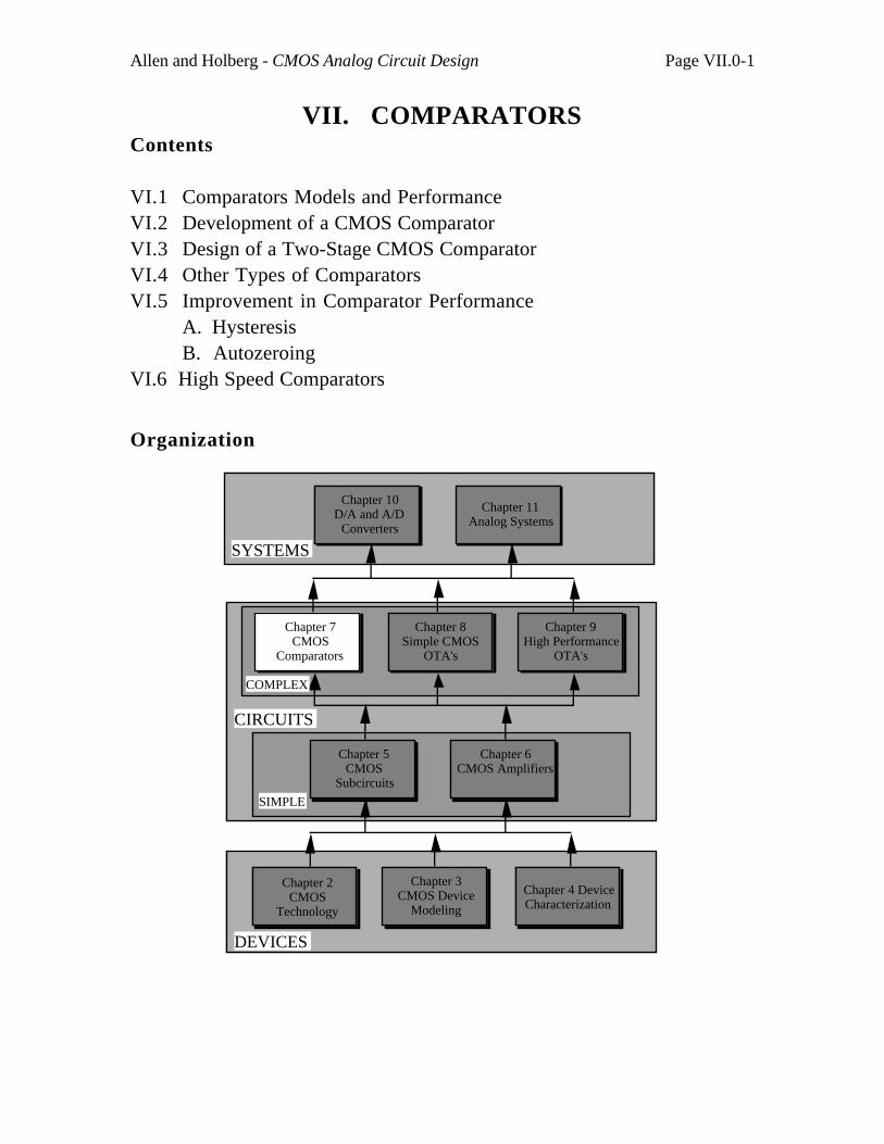
Allen and Holberg - CMOS Analog Circuit Design Page VII.0-1
VII. COMPARATORSContents
VI.1 Comparators Models and PerformanceVI.2 Development of a CMOS ComparatorVI.3 Design of a Two-Stage CMOS ComparatorVI.4 Other Types of ComparatorsVI.5 Improvement in Comparator Performance
A. HysteresisB. Autozeroing
VI.6 High Speed Comparators
Organization
DEVICES
SYSTEMS
CIRCUITS
Chapter 2 CMOS
Technology
Chapter 3 CMOS Device
Modeling
Chapter 4 Device Characterization
Chapter 7 CMOS
Comparators
Chapter 8 Simple CMOS
OTA's
Chapter 9 High Performance
OTA's
Chapter 5 CMOS
Subcircuits
Chapter 6 CMOS Amplifiers
Chapter 10D/A and A/D
Converters
Chapter 11Analog Systems
SIMPLE
COMPLEX

Allen and Holberg - CMOS Analog Circuit Design Page VII.1-1
VII.1 - CHARACTERIZATION OFCOMPARATORS
What is a Comparator?
A comparator is a circuit which compares two analog signals andoutputs a binary signal based on the comparsion. (It can be an op ampwithout frequency compensation.)
Characterization of Comparators
We shall characterize the comparator by the following aspects:
• Resolving capability
• Speed or propagation time delay
• Maximum signal swing limits
• Input offset voltage
• Other Considerations
Noise
Power
Etc.
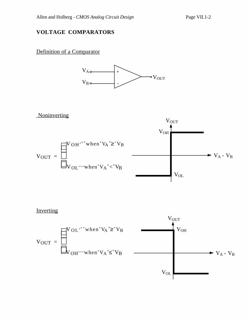
Allen and Holberg - CMOS Analog Circuit Design Page VII.1-2
VOLTAGE COMPARATORS
Definition of a Comparator
+
-
VA
VB
VOUT
VOUT
VA - VB
VOH
VOL
Noninverting
VOUT =
V O H when VA ≥ VB
VOL when VA < VB
VOUT
VA - VB
VOH
VOL
Inverting
VOUT =
V OL when VA ≥ VB
VOH when VA ≤ VB
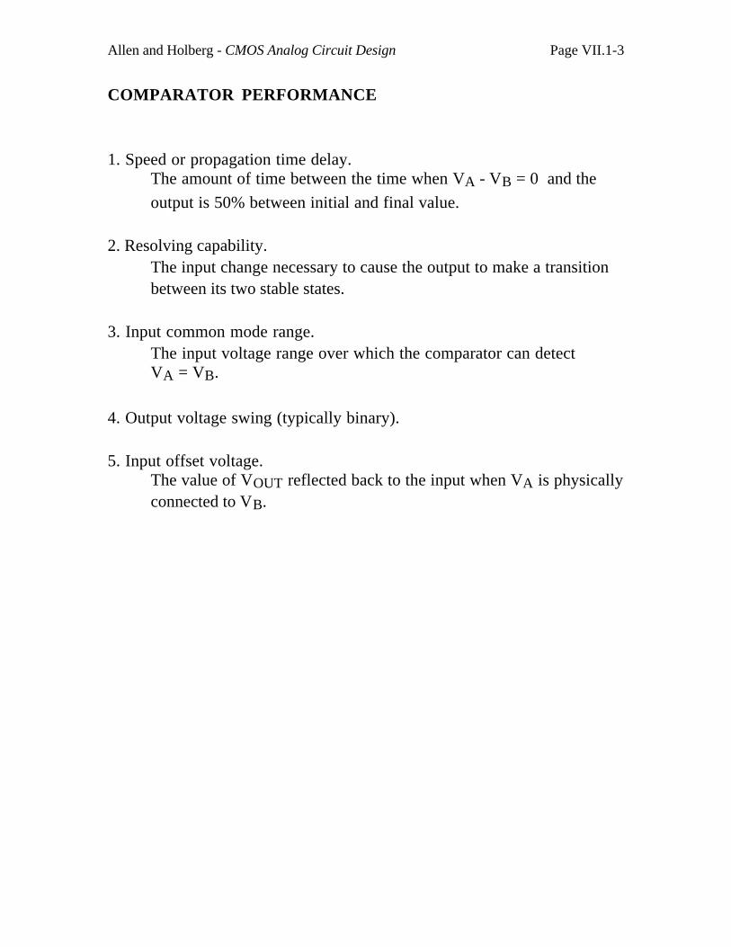
Allen and Holberg - CMOS Analog Circuit Design Page VII.1-3
COMPARATOR PERFORMANCE
1. Speed or propagation time delay.The amount of time between the time when VA - VB = 0 and the
output is 50% between initial and final value.
2. Resolving capability.The input change necessary to cause the output to make a transitionbetween its two stable states.
3. Input common mode range.The input voltage range over which the comparator can detectVA = VB.
4. Output voltage swing (typically binary).
5. Input offset voltage.The value of VOUT reflected back to the input when VA is physicallyconnected to VB.
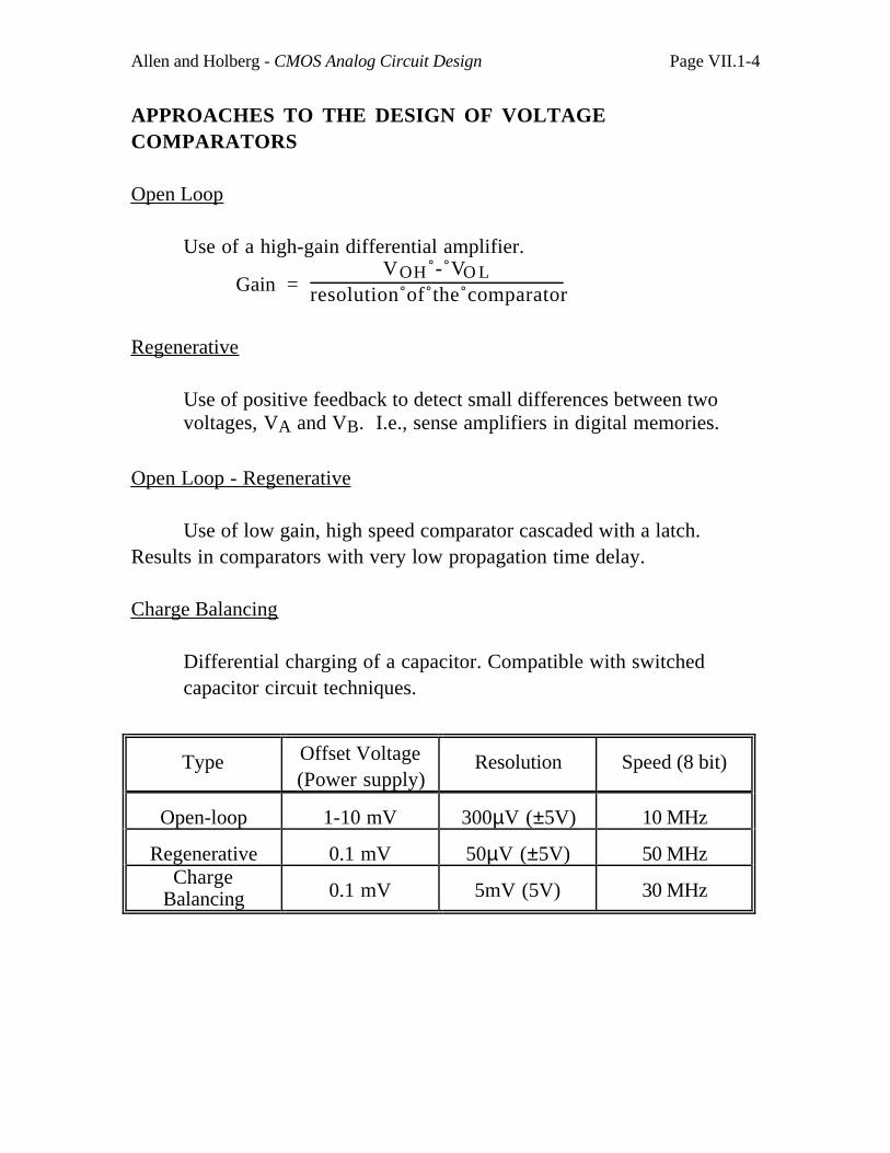
Allen and Holberg - CMOS Analog Circuit Design Page VII.1-4
APPROACHES TO THE DESIGN OF VOLTAGECOMPARATORS
Open Loop
Use of a high-gain differential amplifier.
Gain = VOH - VO L
resolution of the comparator
Regenerative
Use of positive feedback to detect small differences between twovoltages, VA and VB. I.e., sense amplifiers in digital memories.
Open Loop - Regenerative
Use of low gain, high speed comparator cascaded with a latch.Results in comparators with very low propagation time delay.
Charge Balancing
Differential charging of a capacitor. Compatible with switchedcapacitor circuit techniques.
Type Offset Voltage(Power supply)
Resolution Speed (8 bit)
Open-loop 1-10 mV 300µV (±5V) 10 MHz
Regenerative 0.1 mV 50µV (±5V) 50 MHzCharge
Balancing 0.1 mV 5mV (5V) 30 MHz
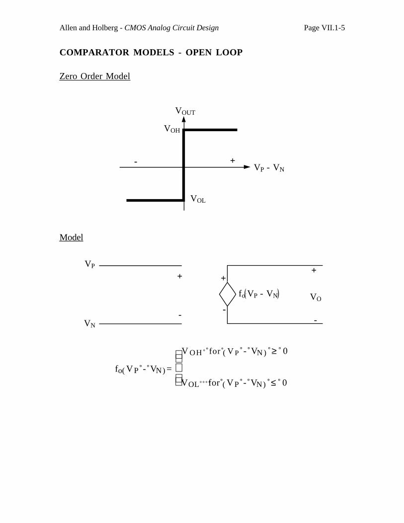
Allen and Holberg - CMOS Analog Circuit Design Page VII.1-5
COMPARATOR MODELS - OPEN LOOP
Zero Order Model
VOUT
VOH
VOL
VP - VN+-
Model
+
-
fo VP - VN
+
-
VO
+
-
VP
VN
fo( )V P - VN =
V OH for ( )V P - VN ≥ 0
VOL for ( )V P - VN ≤ 0
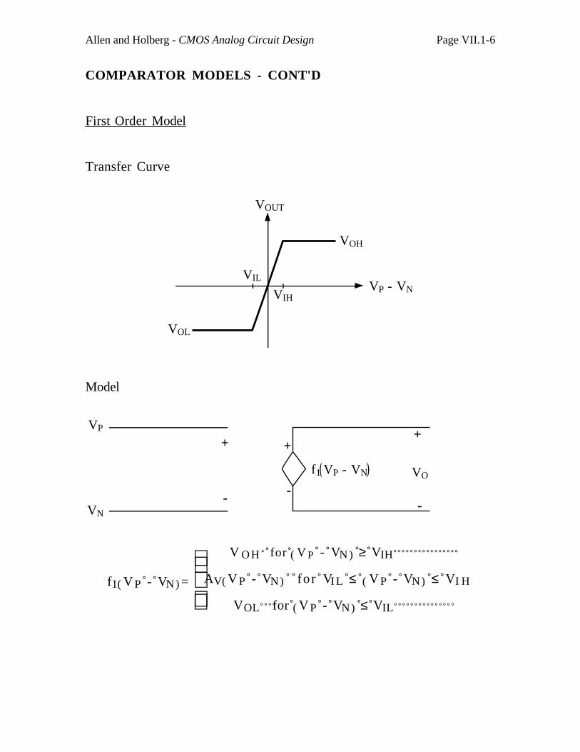
Allen and Holberg - CMOS Analog Circuit Design Page VII.1-6
COMPARATOR MODELS - CONT'D
First Order Model
Transfer Curve
VOUT
VOH
VOL
VP - VNVIH
VIL
Model
+
-
+
-
VO
+
-
VP
VN
f1 VP - VN
f1( )V P - VN =
V O H for ( )V P - VN ≥ VIH
AV( )V P - VN for VI L ≤ ( )V P - VN ≤ VI H
VOL for ( )V P - VN ≤ VIL
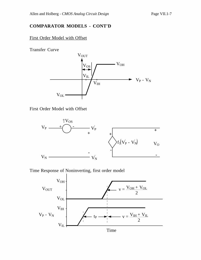
Allen and Holberg - CMOS Analog Circuit Design Page VII.1-7
COMPARATOR MODELS - CONT'D
First Order Model with Offset
Transfer CurveVOUT
VOH
VOL
VP - VNVIH
VIL
VOS
First Order Model with Offset
f1 VP' - VN
'
VP'
VN'
+
-
+
-
VO
+
-
VP
VN
+ -VOS+-
Time Response of Noninverting, first order model
VOUT
VOH
VOL
VP - VN
VIH
VIL
tP
Time
v = VOH + VOL
2
v = VIH + VIL
2
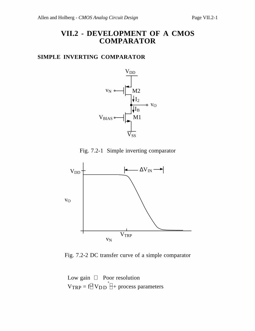
Allen and Holberg - CMOS Analog Circuit Design Page VII.2-1
VII.2 - DEVELOPMENT OF A CMOSCOMPARATOR
SIMPLE INVERTING COMPARATOR
M2
M1
I2
IBvO
vN
VBIAS
VDD
VSS
Fig. 7.2-1 Simple inverting comparator
VDD
vO
vNVTRP
∆VIN
Fig. 7.2-2 DC transfer curve of a simple comparator
Low gain ⇒ Poor resolution
VTRP = f VD D + process parameters
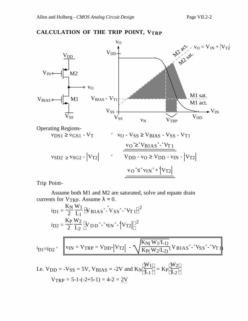
Allen and Holberg - CMOS Analog Circuit Design Page VII.2-2
CALCULATION OF THE TRIP POINT, VTRP
M2
M1
vO
VBIAS
VDD
VSS
VIN
VDD
vN VTRP
vO
VINVDD
M1 sat.M1 act.
M2 ac
t.
M2 sa
t.
VSS
VSS
VBIAS - VT1
vO = VIN + VT2
Operating Regions-vDS1 ≥ vGS1 - VT ‘ vO - VSS ≥ VBIAS - VSS - VT1
vO ≥ VBIAS - VT 1
vSD2 ≥ vSG2 - VT2 ‘ VDD - vO ≥ VDD - vIN - VT2
v O ≤ vIN + VT2
Trip Point-
Assume both M1 and M2 are saturated, solve and equate draincurrents for VTRP. Assume λ ≈ 0.
iD1 = KN2
W1L1
VBIAS - VSS - VT 1 2
iD2 = KP2
W2L2
V D D - vIN - VT2
2
iD1=iD2 ‘ vIN = VTRP = VDD- VT2 - KN( )W1/L1
KP( )W2/L2( )VBIAS - VSS - VT 1
I.e. VDD = -VSS = 5V, VBIAS = -2V and KN
W1
L1 = KP
W2
L2
VTRP = 5-1-(-2+5-1) = 4-2 = 2V
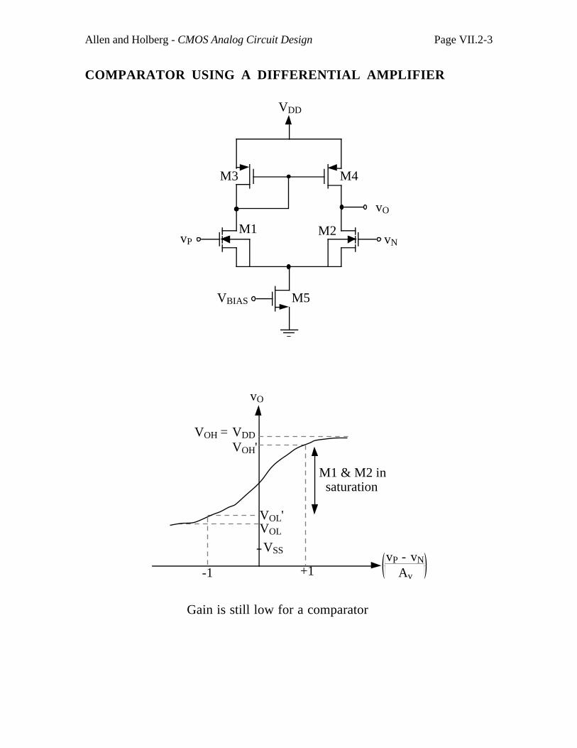
Allen and Holberg - CMOS Analog Circuit Design Page VII.2-3
COMPARATOR USING A DIFFERENTIAL AMPLIFIER
vO
VBIAS
VDD
M3 M4
M1 M2
M5
vP vN
VOH = VDD
VOH'
VOL
VOL'
VSS
+1-1
vO
vP - vN
Av
M1 & M2 in saturation
Gain is still low for a comparator
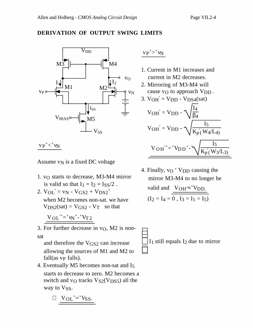
Allen and Holberg - CMOS Analog Circuit Design Page VII.2-4
DERIVATION OF OUTPUT SWING LIMITS
vO
VBIAS
M3 M4
M1 M2
M5
vP vN
VDD
VSS
I1 I2
ISS
vP < vN
Assume vN is a fixed DC voltage
1. vO starts to decrease, M3-M4 mirror is valid so that I1 = I2 = ISS/2 .2. VOL' = vN - VGS2 + VDS2
when M2 becomes non-sat. we have VDS2(sat) = VGS2 - VT so that
VOL' = vN - VT 2
3. For further decrease in vO, M2 is non-
sat and therefore the VGS2 can increase
allowing the sources of M1 and M2 to fall(as vP falls).4. Eventually M5 becomes non-sat and I5
starts to decrease to zero. M2 becomes a switch and vO tracks VS2(VDS5) all the way to VSS.
∴ VOL = VSS.
vP > vN
1. Current in M1 increases and current in M2 decreases.2. Mirroring of M3-M4 will cause vO to approach VDD .3. VOH' = VDD - VDS4(sat)
VOH' = VDD - I4β4
VOH' = VDD - I5
Kp'( )W4/L4
V O H ' = VD D - I5
Kp'( )W3/L3
4. Finally, vO ‘ VDD causing the
mirror M3-M4 to no longer be
valid and VOH ≈ VDD.
(I2 = I4 = 0 , I3 = I1 = I5)
I1 still equals I2 due to mirror
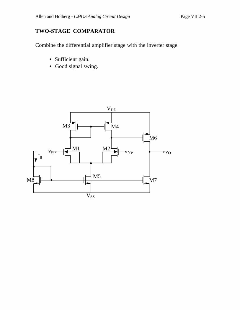
Allen and Holberg - CMOS Analog Circuit Design Page VII.2-5
TWO-STAGE COMPARATOR
Combine the differential amplifier stage with the inverter stage.
• Sufficient gain.• Good signal swing.
vO
VSS
VDD
M3 M4
M5
vPvN
M7
M6
M8
I8
M1 M2
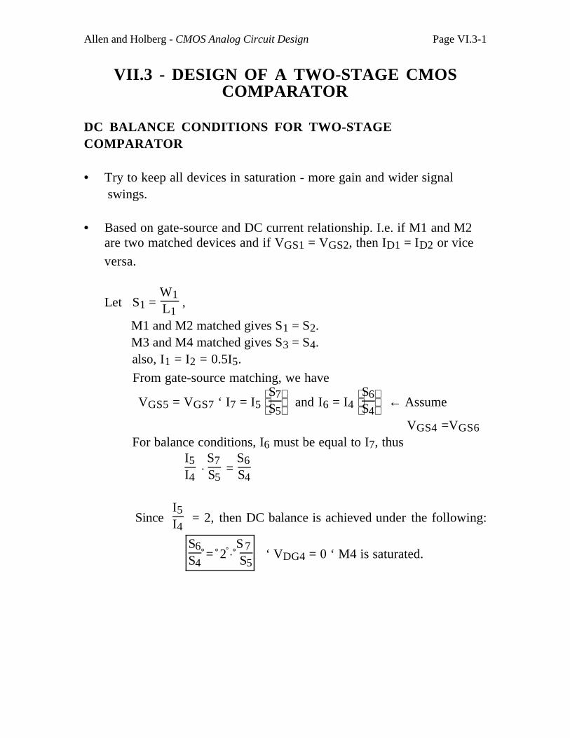
Allen and Holberg - CMOS Analog Circuit Design Page VI.3-1
VII.3 - DESIGN OF A TWO-STAGE CMOSCOMPARATOR
DC BALANCE CONDITIONS FOR TWO-STAGECOMPARATOR
• Try to keep all devices in saturation - more gain and wider signal swings.
• Based on gate-source and DC current relationship. I.e. if M1 and M2are two matched devices and if VGS1 = VGS2, then ID1 = ID2 or vice
versa.
Let S1 = W1L1
,
M1 and M2 matched gives S1 = S2. M3 and M4 matched gives S3 = S4. also, I1 = I2 = 0.5I5.
From gate-source matching, we have
VGS5 = VGS7 ‘ I7 = I5
S7
S5 and I6 = I4
S6
S4 ← Assume
VGS4 =VGS6 For balance conditions, I6 must be equal to I7, thus
I5I4
. S7S5
= S6S4
Since I5I4
= 2, then DC balance is achieved under the following:
S6S4
= 2 . S 7S5
‘ VDG4 = 0 ‘ M4 is saturated.
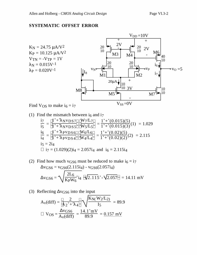
Allen and Holberg - CMOS Analog Circuit Design Page VI.3-2
SYSTEMATIC OFFSET ERROR
KN = 24.75 µA/V2
KP = 10.125 µA/V2
VTN = -VTP = 1VλN = 0.015V-1
λP = 0.020V-1
VSS
vO
VDD
M3 M4
M5
vPvN
M7
M6
M8
I8M1 M2
2010
2010
+
-2V
+
2V-
=10V
=0V
+
-
3V
2010
2010
4010
1010
1010
20µA
i6
i7=5V
Find VOS to make i6 = i7
(1) Find the mismatch between i6 and i7i7i5
=
1 + λNvDS7
1 + λNvDS5
W7/L7
W5/L5 =
1 + (0.015)(5)1 + (0.015)(3) (1) = 1.029
i6i4
=
1 + λPvDS6
1 + λPvDS4
W6/L6
W4/L4 =
1 + (0.02)(5)1 + (0.02)(2) (2) = 2.115
i5 = 2i4∴ i7 = (1.029)(2)i4 = 2.057i4 and i6 = 2.115i4
(2) Find how much vGS6 must be reduced to make i6 = i7 ∆vGS6 = vGS6(2.115i4) - vGS6(2.057i4)
∆vGS6 = 2L6
KPW6 i4 2.115 - 2.057 = 14.11 mV
(3) Reflecting ∆vGS6 into the input
Av(diff) =
2
λ 2 + λ 4
KN( )W2/L2
I5 = 89.9
∴ VOS = ∆vGS6
Av(diff) = 14.1 mV
89.9 = 0.157 mV
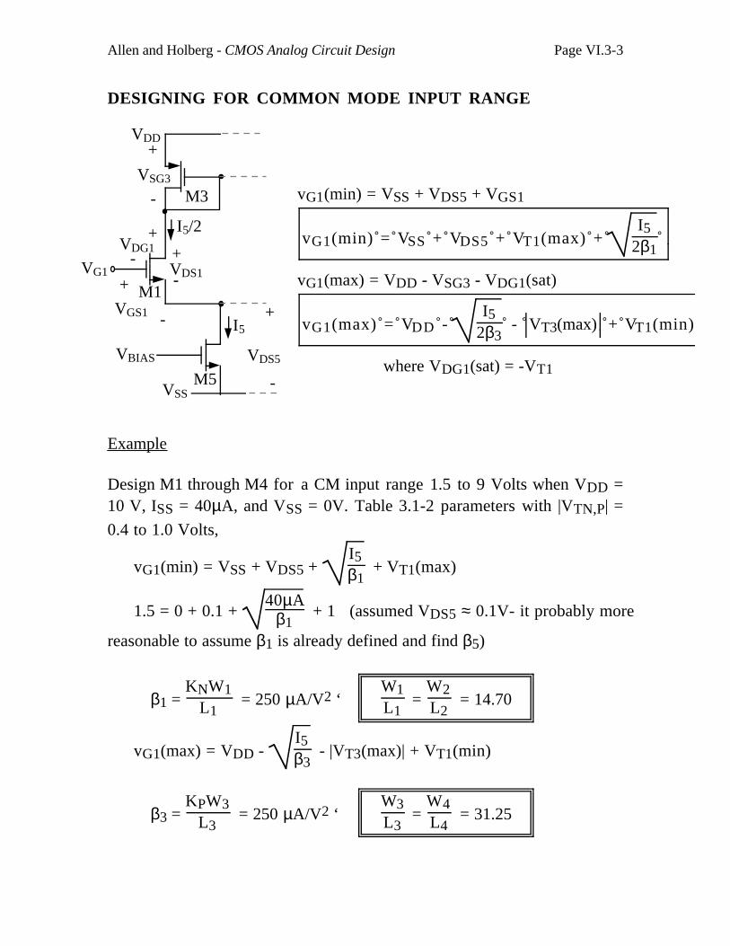
Allen and Holberg - CMOS Analog Circuit Design Page VI.3-3
Example
Design M1 through M4 for a CM input range 1.5 to 9 Volts when VDD =10 V, ISS = 40µA, and VSS = 0V. Table 3.1-2 parameters with |VTN,P| =
0.4 to 1.0 Volts,
vG1(min) = VSS + VDS5 + I5β1
+ VT1(max)
1.5 = 0 + 0.1 + 40µA
β1 + 1 (assumed VDS5 ≈ 0.1V- it probably more
reasonable to assume β1 is already defined and find β5)
β1 = KNW1
L1 = 250 µA/V2 ‘
W1L1
= W2L2
= 14.70
vG1(max) = VDD - I5β3
- |VT3(max)| + VT1(min)
β3 = KPW3
L3 = 250 µA/V2 ‘
W3L3
= W4L4
= 31.25
DESIGNING FOR COMMON MODE INPUT RANGE
VSS
M3
M5
M1
I5
I5/2
VDS1
VDG1
+
-
+
-
+
-
+
-
+
-
VSG3
VGS1
VBIAS
VG1
VDS5
VDD
vG1(min) = VSS + VDS5 + VGS1
vG1(min) = VSS + VDS5 + VT1(max) + I5
2β1
vG1(max) = VDD - VSG3 - VDG1(sat)
vG1(max) = VDD - I5
2β3 - VT3(max) + VT1(min)
where VDG1(sat) = -VT1
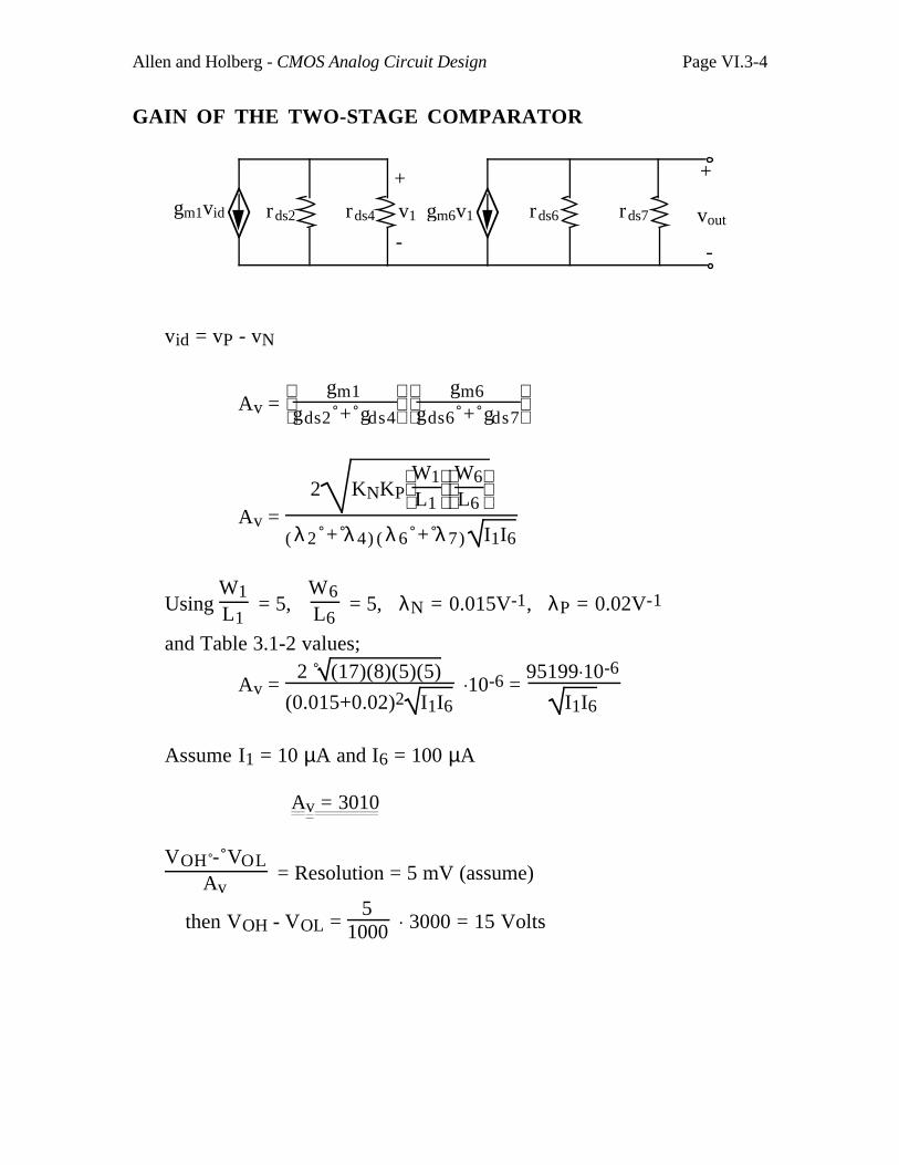
Allen and Holberg - CMOS Analog Circuit Design Page VI.3-4
GAIN OF THE TWO-STAGE COMPARATOR
gm1vid gm6v1
+
-
v1rds2 rds4
+
-
rds6 rds7 vout
vid = vP - vN
Av =
gm1
gds2 + gds4
gm6
gds6 + gds7
Av = 2 KNKP
W1
L1
W6
L6
( )λ 2 + λ 4 ( )λ 6 + λ 7 I1I6
Using W1L1
= 5, W6L6
= 5, λN = 0.015V-1, λP = 0.02V-1
and Table 3.1-2 values;
Av = 2 (17)(8)(5)(5)
(0.015+0.02)2 I1I6 .10-6 =
95199.10-6
I1I6
Assume I1 = 10 µA and I6 = 100 µA
A v = 3010
VOH - VOLAv
= Resolution = 5 mV (assume)
then VOH - VOL = 5
1000 . 3000 = 15 Volts
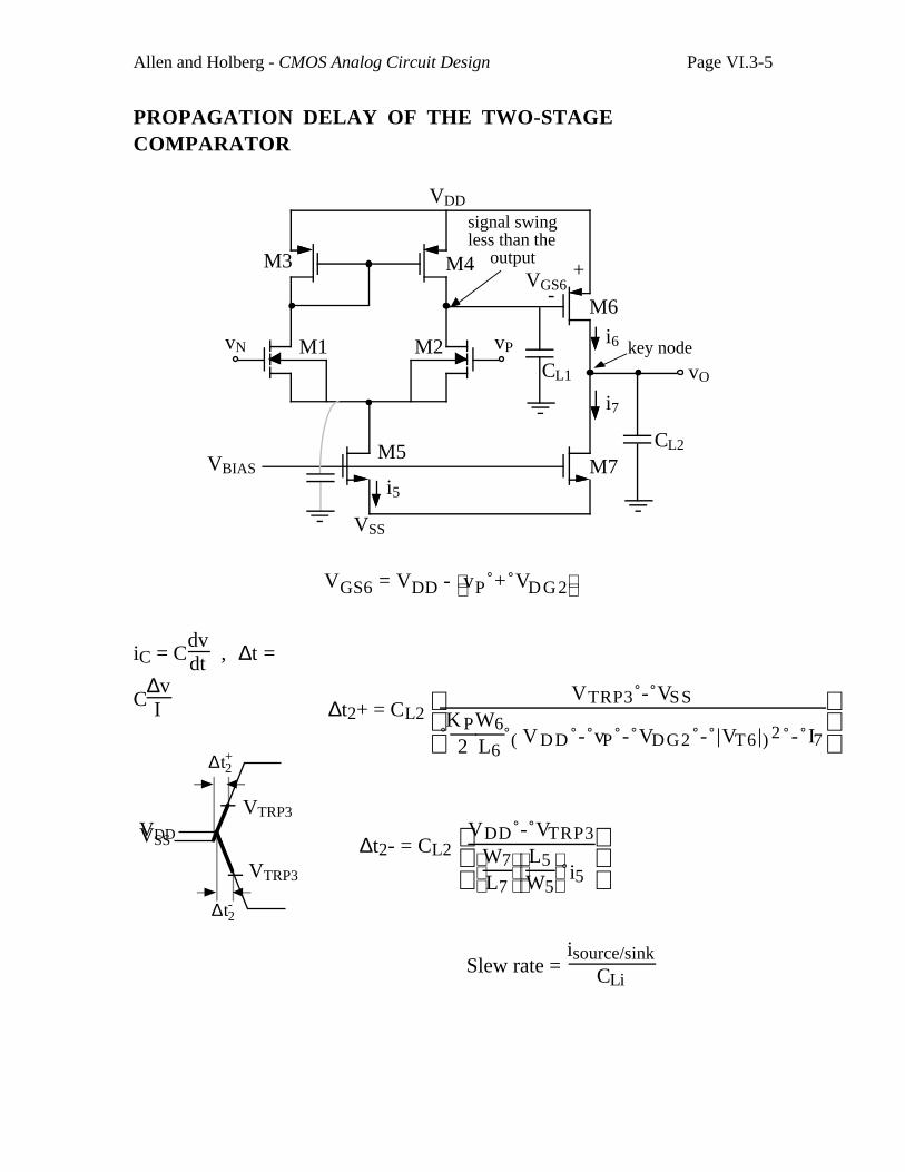
Allen and Holberg - CMOS Analog Circuit Design Page VI.3-5
PROPAGATION DELAY OF THE TWO-STAGECOMPARATOR
vO
VSS
VDD
M3 M4
M5
vPvN
M7
M6
M1 M2
VBIAS
i5
i6
i7
CL1
CL2
+-
key node
signal swingless than the output
VGS6
VGS6 = VDD - vP + VD G 2
iC = Cdvdt , ∆t =
C∆vI
Slew rate = isource/sink
CLi
VTRP3
VSS
∆t2+
∆t2+ = CL2
VTRP3 - VSS
K P
2W6L6
( )V DD - vP - VDG2 - |VT6| 2 - I7
VTRP3
VDD
∆t2-
∆t2- = CL2
VDD - VTRP3
W7
L7
L5
W5 i5
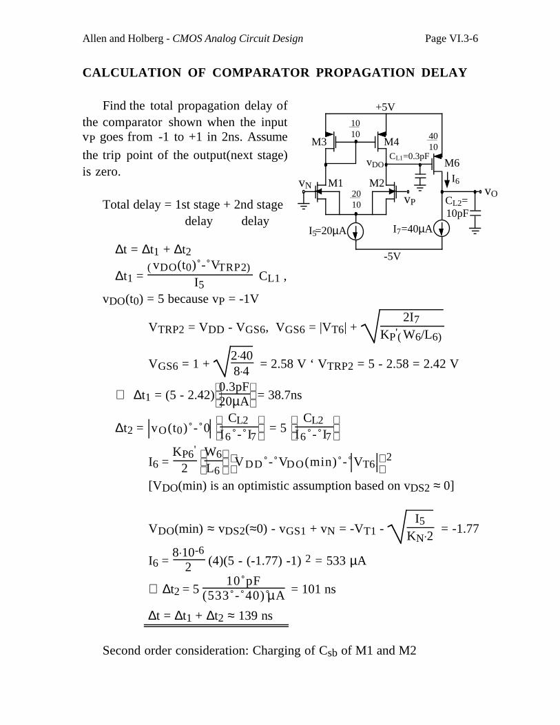
Allen and Holberg - CMOS Analog Circuit Design Page VI.3-6
CALCULATION OF COMPARATOR PROPAGATION DELAY
Find the total propagation delay ofthe comparator shown when the inputvP goes from -1 to +1 in 2ns. Assume
the trip point of the output(next stage)is zero.
Total delay = 1st stage + 2nd stage delay delay
∆t = ∆t1 + ∆t2
∆t1 = ( )vDO(t0) - VTRP2
I5 CL1 ,
vDO(t0) = 5 because vP = -1V
VTRP2 = VDD - VGS6, VGS6 = |VT6| + 2I7
KP'( )W6/L6
VGS6 = 1 + 2.408.4
= 2.58 V ‘ VTRP2 = 5 - 2.58 = 2.42 V
∴ ∆t1 = (5 - 2.42)
0.3pF
20µA = 38.7ns
∆t2 = vO(t0) - 0
CL2
I6 - I7 = 5
CL2
I6 - I7
I6 = KP6'
2
W6
L6
VDD - VDO(min) - VT6 2
[VDO(min) is an optimistic assumption based on vDS2 ≈ 0]
VDO(min) ≈ vDS2(≈0) - vGS1 + vN = -VT1 - I5
KN.2 = -1.77
I6 = 8.10-6
2 (4)(5 - (-1.77) -1) 2 = 533 µA
∴ ∆t2 = 5 10 pF
(533 - 40) µA = 101 ns
∆t = ∆t1 + ∆t2 ≈ 139 ns
Second order consideration: Charging of Csb of M1 and M2
vOvP
vN M1 M2
I5=20µA
-5V
I7=40µA
M3 M4CL1=0.3pF
M6
+5V
vDO
1010
2010
4010
I6
CL2=10pF
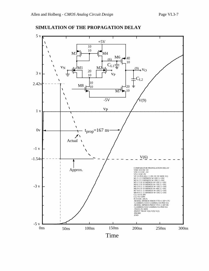
Allen and Holberg - CMOS Analog Circuit Design Page VI.3-7
-5 v
-3 v
-1 v
1 v
3 v
5 v
Time0ns 50ns 100ns 150ns 200ns 250ns 300ns
-1.54v
2.42v
vP
V(9)
V(6)
0v tprop=167 ns
vOvP
vN M1 M2
-5V
M3 M4M6
+5V1010
2010
4010
M7
CL1
CL2
M81010 20
10
Actual
Approx.
(9)
(6)
COMPARATOR PROPAGATION DELAYVDD 10 0 DC 5VVSS 11 0 DC -5VVN 1 0 DC 0VVP 2 0 PULSE(-1 1 0N 1N 1N 500N 1U)M1 3 1 5 5 MNMOS W=20U L=10UM2 6 2 5 5 MNMOS W=20U L=10UM3 3 3 10 10 MPMOS W=10U L=10UM4 6 3 10 10 MPMOS W=10U L=10UM5 5 8 11 11 MNMOS W=10U L=10UM6 9 6 10 10 MPMOS W=40U L=10UM7 9 8 11 11 MNMOS W=20U L=10UM8 8 8 11 11 MNMOS W=10U L=10UCL1 6 0 0.3PFCL2 9 0 10PFIS 0 8 DC 20UA.MODEL MNMOS NMOS VTO=1 KP=17U+LAMBDA=0.015 GAMMA=0.8 PHI=0.6.MODEL MPMOS PMOS VTO=-1 KP=8U+LAMBDA=0.02 GAMMA=0.4 PHI=0.6.TRAN 2N 300N.PRINT TRAN V(6) V(9) V(2).PROBE.END
SIMULATION OF THE PROPAGATION DELAY
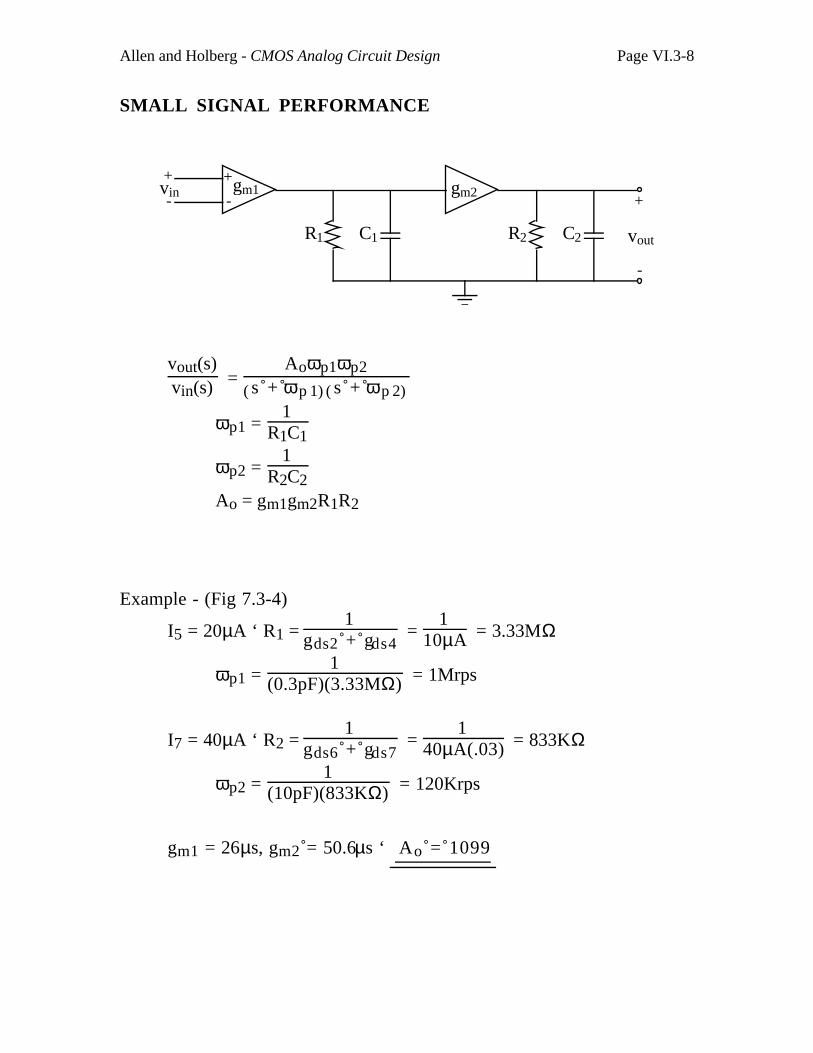
Allen and Holberg - CMOS Analog Circuit Design Page VI.3-8
SMALL SIGNAL PERFORMANCE
R1 R2 C2C1
gm1+
-
+
- +
-
vin
vout
gm2
vout(s)vin(s) =
Aoωp1ωp2
( )s + ωp 1 ( )s + ωp 2
ωp1 = 1
R1C1
ωp2 = 1
R2C2
Ao = gm1gm2R1R2
Example - (Fig 7.3-4)
I5 = 20µA ‘ R1 = 1
gds2 + gds4 =
110µA = 3.33MΩ
ωp1 = 1
(0.3pF)(3.33MΩ) = 1Mrps
I7 = 40µA ‘ R2 = 1
gds6 + gds7 =
140µA(.03) = 833KΩ
ωp2 = 1
(10pF)(833KΩ) = 120Krps
gm1 = 26µs, gm2 = 50.6µs ‘ Ao = 1099
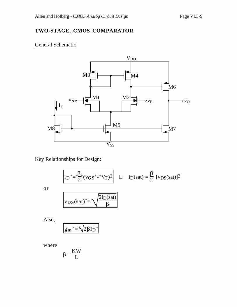
Allen and Holberg - CMOS Analog Circuit Design Page VI.3-9
TWO-STAGE, CMOS COMPARATOR
General Schematic
vO
VSS
VDD
M3 M4
M5
vPvN
M7
M6
M8
I8
M1 M2
Key Relationships for Design:
iD = β2 (vGS - VT)2 ⇒ iD(sat) =
β2 [vDS(sat)]2
or
vDS(sat) = 2iD(sat)
β
Also,
g m = 2βID
where
β = KW
L

Allen and Holberg - CMOS Analog Circuit Design Page VI.3-10
COMPARATOR DESIGN PROCEDURE
1. Set the output current to meet the slew rate requirements.
i = CdVdt
2. Determine the minimum sizes for M6 and M7 for the proper ouput
voltage swing.
vDS(sat) = 2IDβ
3. Knowing the second stage current and minimum device size for M6,
calculate the second stage gain.
A2 = -gm6
gds6 + gds7
4. Calculate the required first stage gain from A2 and gain specifications.
5. Determine the current in the first stage based upon proper mirroring
and minimum values for M6 and M7. Verify that Pdiss is met.
6. Calculate the device size of M1 from A1 and IDS1.
A1 = -gm1
gds1 + gds3 and gm1 =
2K'W/LIDS1
7. Design minimum device size for M5 based on negative CMR require-
ment using the following (IDS1 = 0.5IDS5):
vG1(min) = VSS + VDS5 + IDS5β1
+ VT1(max)
where VDS5 = 2IDS5
β5 = VDS5(sat)
8. Increase either M5 or M7 for proper mirroring.
9. Design M4 for proper positive CMR using:
vG1(max) = VDD - IDS5β3
- VTO3 (max) + VT1
10. Increase M3 or M6 for proper mirroring.
11. Simulate circuit.
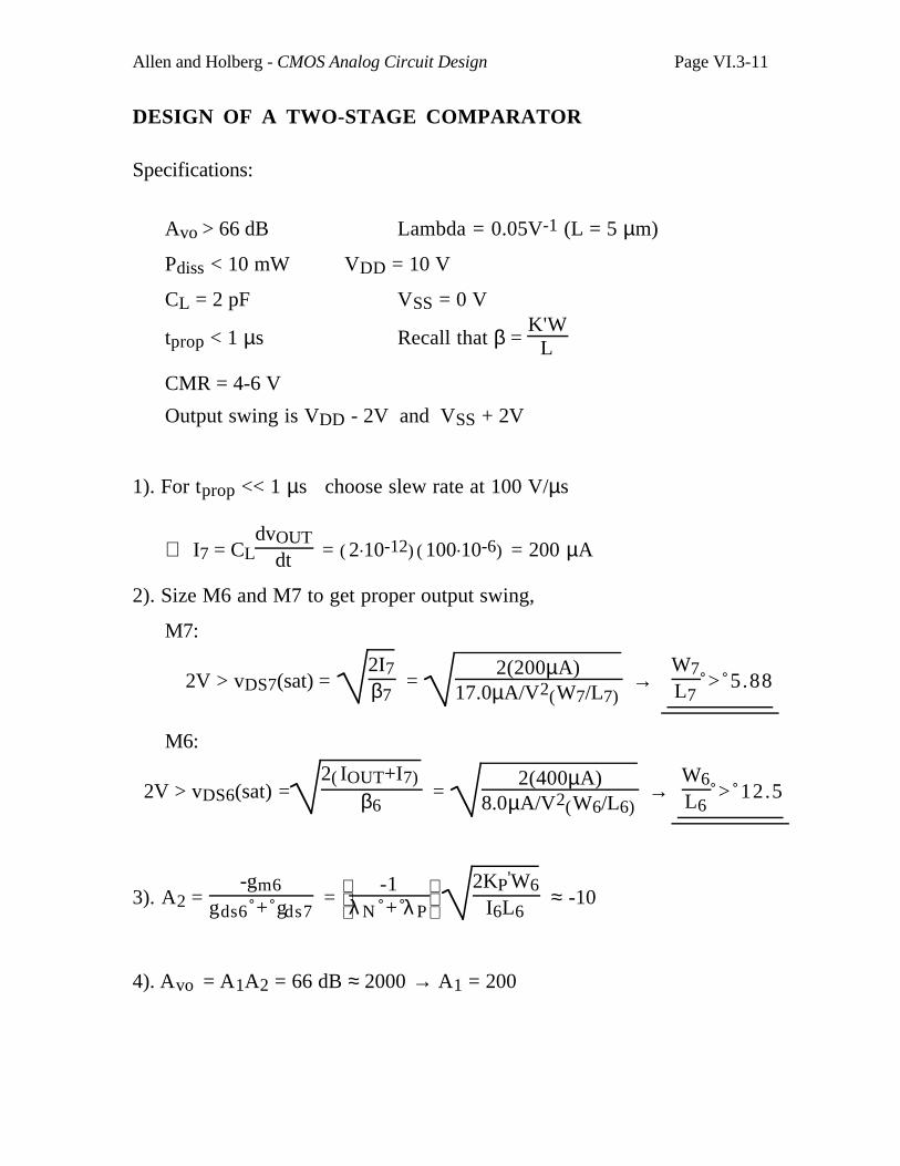
Allen and Holberg - CMOS Analog Circuit Design Page VI.3-11
DESIGN OF A TWO-STAGE COMPARATOR
Specifications:
Avo > 66 dB Lambda = 0.05V-1 (L = 5 µm)
Pdiss < 10 mW VDD = 10 V
CL = 2 pF VSS = 0 V
tprop < 1 µs Recall that β = K'W
L
CMR = 4-6 V
Output swing is VDD - 2V and VSS + 2V
1). For tprop << 1 µs choose slew rate at 100 V/µs
∴ I7 = CLdvOUT
dt = ( )2.10-12 ( )100.10-6 = 200 µA
2). Size M6 and M7 to get proper output swing,
M7:
2V > vDS7(sat) = 2I7β7
= 2(200µA)
17.0µA/V2( )W7/L7 →
W7L7
> 5.88
M6:
2V > vDS6(sat) =2( )IOUT+I7
β6 =
2(400µA)8.0µA/V2( )W6/L6
→W6L6
> 12.5
3). A2 = -gm6
gds6 + gds7 =
-1
λ N + λ P
2KP'W6I6L6
≈ -10
4). Avo = A1A2 = 66 dB ≈ 2000 → A1 = 200
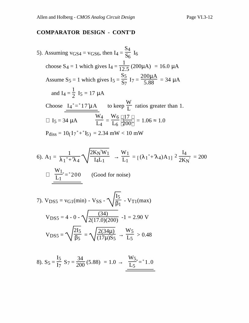
Allen and Holberg - CMOS Analog Circuit Design Page VI.3-12
COMPARATOR DESIGN - CONT'D
5). Assuming vGS4 = vGS6, then I4 = S4S6
I6
choose S4 = 1 which gives I4 = 1
12.5 (200µA) = 16.0 µA
Assume S5 = 1 which gives I5 = S5S7
I7 = 200µA
5.88 = 34 µA
and I4 = 12 I5 = 17 µA
Choose I4 = 17 µA to keep WL ratios greater than 1.
∴ I5 = 34 µAW4L4
= W6L6
17
200 = 1.06 ≈ 1.0
Pdiss = 10( )I7 + I5 = 2.34 mW < 10 mW
6). A1 = 1
λ 1 + λ 4
2KN'W1I4L1
→ W1L1
= [ ](λ1 + λ4)A1 2 I4
2KN' = 200
∴ W1L1
= 200 (Good for noise)
7). VDS5 = vG1(min) - VSS - I5β1
- VT1(max)
VDS5 = 4 - 0 - (34)
2(17.0)(200) -1 = 2.90 V
VDS5 = 2I5β5
= 2(34µ)(17µ)S5
→ W5L5
> 0.48
8). S5 = I5I7
S7 = 34200 (5.88) = 1.0 →
W5L5
= 1 .0
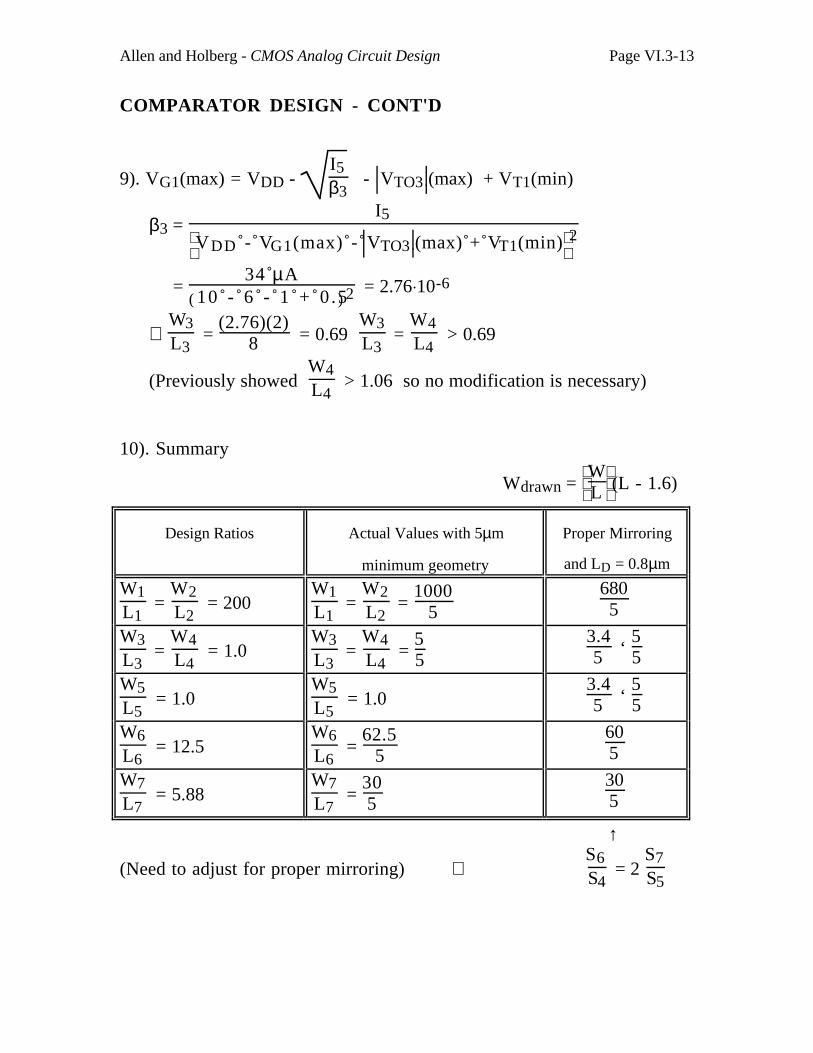
Allen and Holberg - CMOS Analog Circuit Design Page VI.3-13
COMPARATOR DESIGN - CONT'D
9). VG1(max) = VDD - I5β3
- VTO3 (max) + VT1(min)
β3 = I5
VDD - VG1(max) - VTO3 (max) + VT1(min) 2
= 34 µA
( )10 - 6 - 1 + 0 .5 2 = 2.76.10-6
∴ W3L3
= (2.76)(2)
8 = 0.69 W3L3
= W4L4
> 0.69
(Previously showed W4L4
> 1.06 so no modification is necessary)
10). Summary
Wdrawn =
W
L (L - 1.6)
Design Ratios Actual Values with 5µm
minimum geometry
Proper Mirroring
and LD = 0.8µm
W1L1
= W2L2
= 200W1L1
= W2L2
= 1000
5 6805
W3L3
= W4L4
= 1.0W3L3
= W4L4
= 55
3.45 ‘
55
W5L5
= 1.0W5L5
= 1.03.45 ‘
55
W6L6
= 12.5W6L6
= 62.5
5 605
W7L7
= 5.88W7L7
= 305
305
↑
(Need to adjust for proper mirroring) ⇒ S6S4
= 2 S7S5

Allen and Holberg - CMOS Analog Circuit Design Page VII.4-1
VII.4 - OTHER TYPES OF COMPARATORS
FOLDED CASCODE CMOS COMPARATOR
Circuit Diagram
VSS
MN1 MN2
MP3 MP4
MN5MN9
MP8
MP6
MN25
MN24 MN7
MP12 MP13
MN10 MN11
VDD
vOUT
v1v2
Small Signal Model
gm1v2 gm2v1
1gm12
1gm13i1 i2
i1i2rout vout
+
-
whereRout ≈ (rds5gm11rds11)||((rds4||rds2)gm13rds13) =
= 1
gds5gds11gm11
+ (gds2+gds4)gds13
gm13
The small signal voltage gain is
vout = rout(i2-i1) = (gm2+gm1)Routvin =
gm1+gm2
gds5gds11gm11
+ (gds2+gds4)gds13
gm13
vin
where vin = v1 - v2.
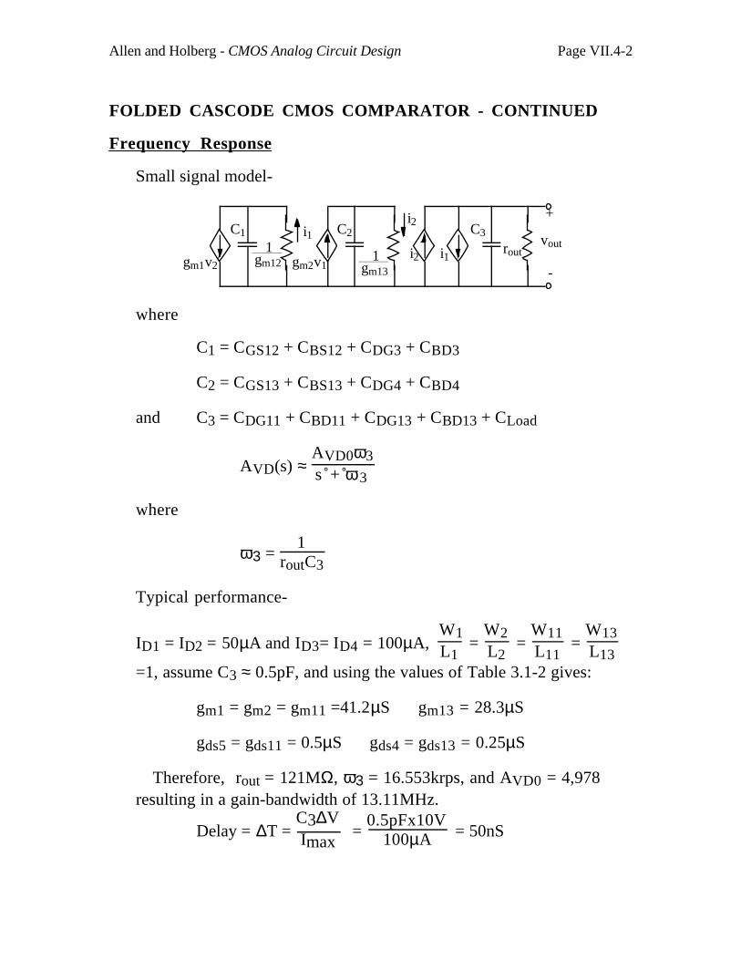
Allen and Holberg - CMOS Analog Circuit Design Page VII.4-2
FOLDED CASCODE CMOS COMPARATOR - CONTINUED
Frequency Response
Small signal model-
gm1v2 gm2v1
1gm12 1
gm13
i1i2
i1i2 routvout
+
-
C1 C2 C3
where
C1 = CGS12 + CBS12 + CDG3 + CBD3
C2 = CGS13 + CBS13 + CDG4 + CBD4
and C3 = CDG11 + CBD11 + CDG13 + CBD13 + CLoad
AVD(s) ≈ AVD0ω3s + ω3
where
ω3 = 1
routC3
Typical performance-
ID1 = ID2 = 50µA and ID3= ID4 = 100µA, W1L1
= W2L2
= W11L11
= W13L13
=1, assume C3 ≈ 0.5pF, and using the values of Table 3.1-2 gives:
gm1 = gm2 = gm11 =41.2µS gm13 = 28.3µS
gds5 = gds11 = 0.5µS gds4 = gds13 = 0.25µS
Therefore, rout = 121MΩ, ω3 = 16.553krps, and AVD0 = 4,978resulting in a gain-bandwidth of 13.11MHz.
Delay = ∆T = C3∆VImax =
0.5pFx10V100µA = 50nS
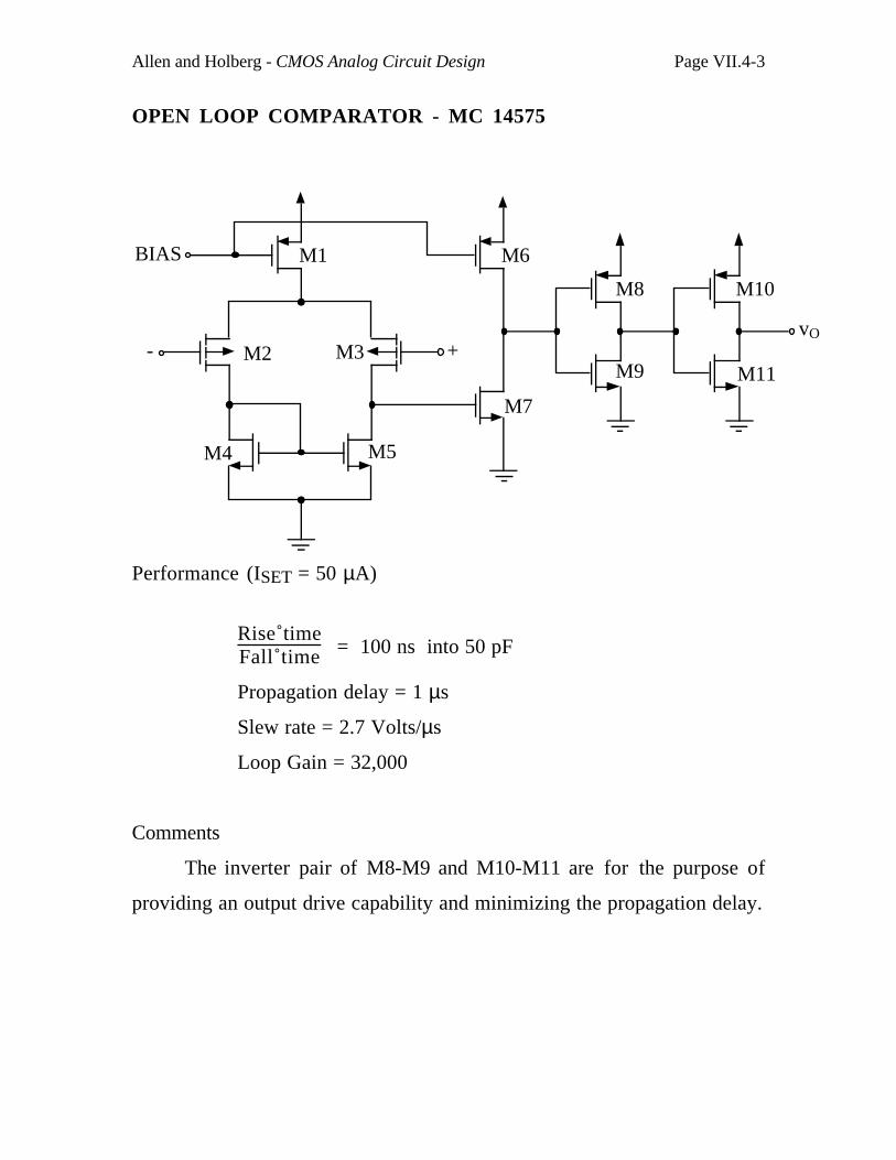
Allen and Holberg - CMOS Analog Circuit Design Page VII.4-3
OPEN LOOP COMPARATOR - MC 14575
M4 M5
M7
M6M1BIAS
M3M2- +
M8
M9
M10
M11
vO
Performance (ISET = 50 µA)
Rise timeFall time = 100 ns into 50 pF
Propagation delay = 1 µs
Slew rate = 2.7 Volts/µs
Loop Gain = 32,000
Comments
The inverter pair of M8-M9 and M10-M11 are for the purpose of
providing an output drive capability and minimizing the propagation delay.
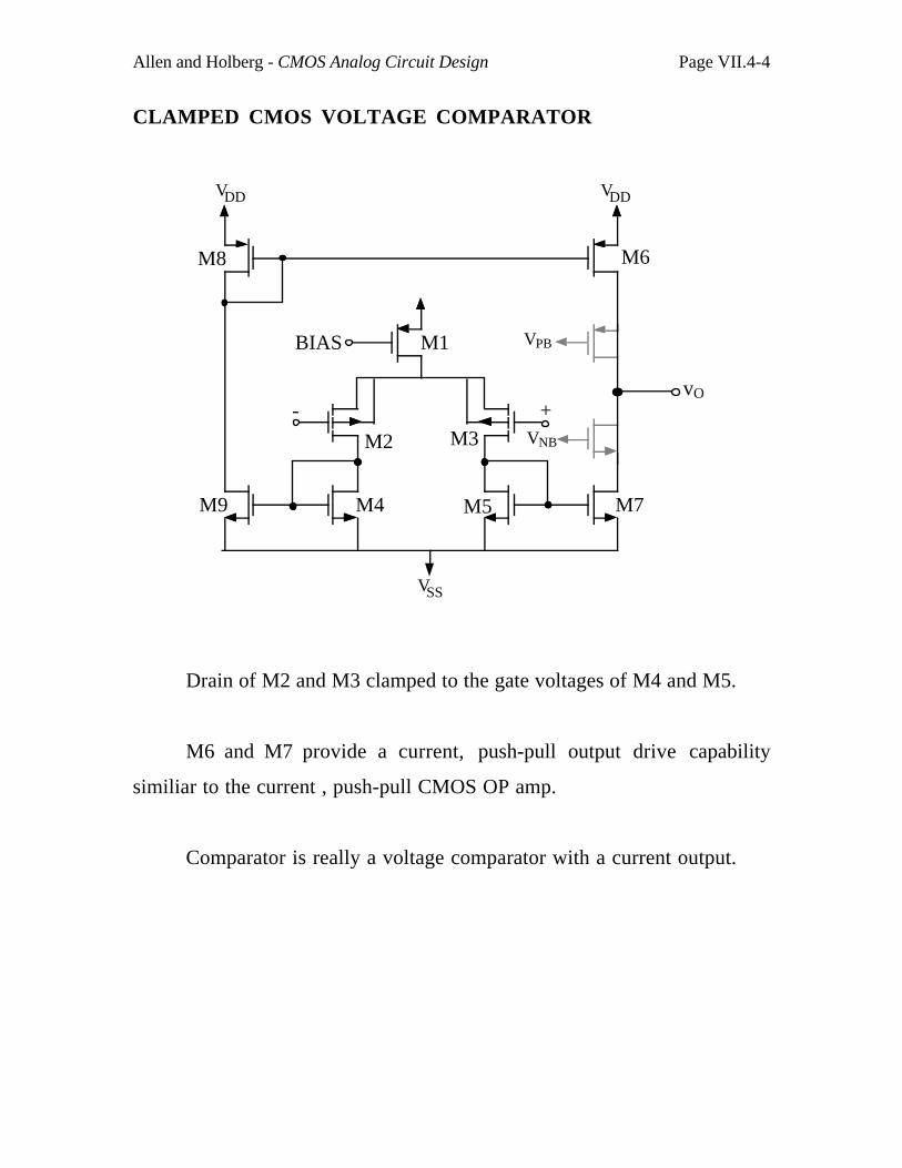
Allen and Holberg - CMOS Analog Circuit Design Page VII.4-4
CLAMPED CMOS VOLTAGE COMPARATOR
M4 M5 M7
M6
M1BIAS
M3M2
- +
M8
M9
vO
VDD VDD
VSS
VNB
VPB
Drain of M2 and M3 clamped to the gate voltages of M4 and M5.
M6 and M7 provide a current, push-pull output drive capability
similiar to the current , push-pull CMOS OP amp.
Comparator is really a voltage comparator with a current output.
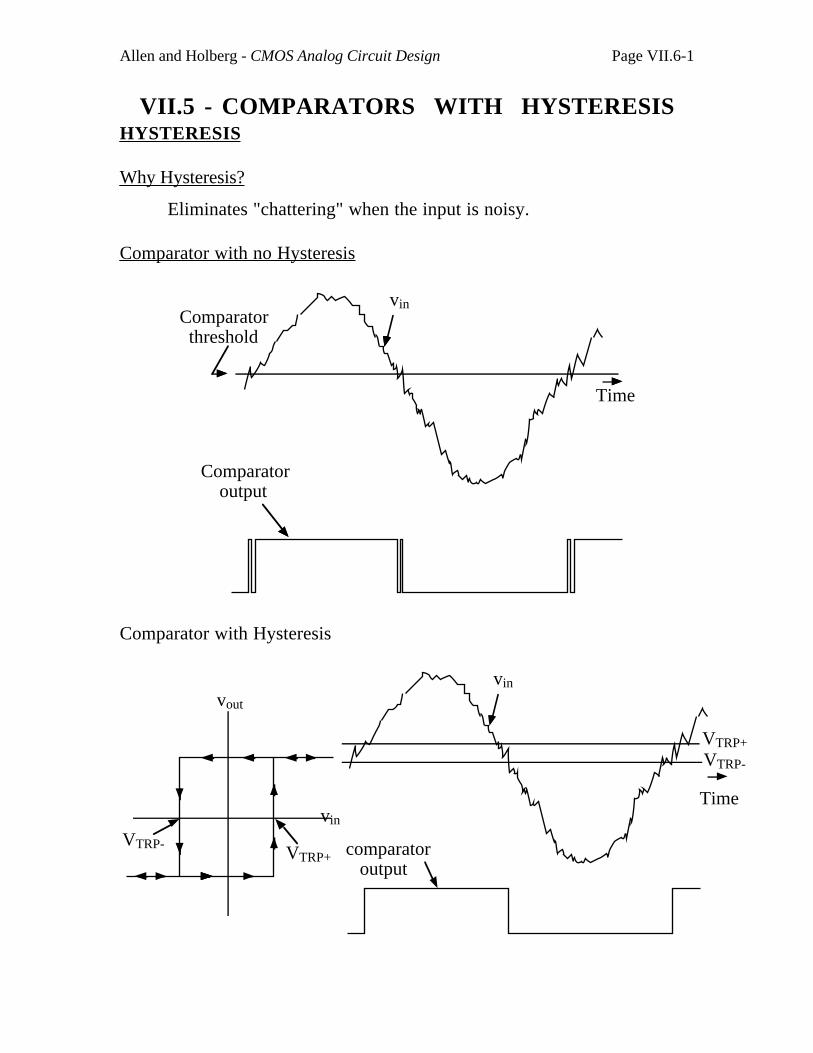
Allen and Holberg - CMOS Analog Circuit Design Page VII.6-1
VII.5 - COMPARATORS WITH HYSTERESIS HYSTERESIS
Why Hysteresis?
Eliminates "chattering" when the input is noisy.
Comparator with no Hysteresis
Comparator threshold
vin
Comparator output
Time
Comparator with Hysteresis
VTRP+VTRP-
vin
vout
vin
Time
comparator output
VTRP+
VTRP-
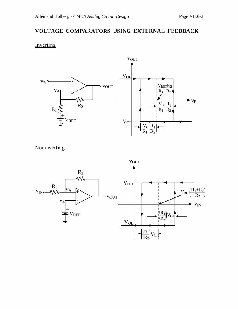
Allen and Holberg - CMOS Analog Circuit Design Page VII.6-2
VOLTAGE COMPARATORS USING EXTERNAL FEEDBACK
Inverting
-
+vOUT
vB
vA
R1R2
VREF+-
VOH
VOL
vB
vOUT
VREFR2R1+R2
VOHR1R1+R2
VOLR1R1+R2
Noninverting
-
+vOUT
vB
vAR1
R2
VREF+-
vIN
R1R2
VOH
vIN
VOL
VOH
VREFR1+R2
R2
R1R2
VOL
vOUT
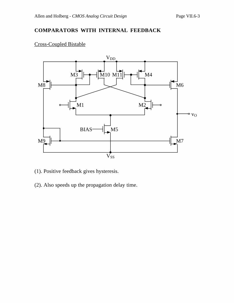
Allen and Holberg - CMOS Analog Circuit Design Page VII.6-3
COMPARATORS WITH INTERNAL FEEDBACK
Cross-Coupled Bistable
M4
M5
M7
M6
M1
BIAS
M3
M2
M8
M9
vO
M10 M11
VSS
VDD
(1). Positive feedback gives hysteresis.
(2). Also speeds up the propagation delay time.
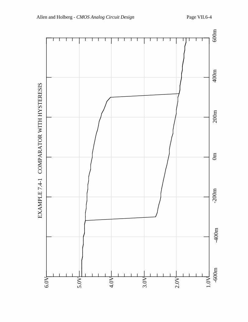
Allen and Holberg - CMOS Analog Circuit Design Page VII.6-4
1.0V
2.0V
3.0V
4.0V
5.0V
6.0V -6
00m
-400
m-2
00m
0m20
0m40
0m60
0m
EX
AM
PLE
7.4
-1
CO
MPA
RA
TO
R W
ITH
HY
STE
RE
SIS
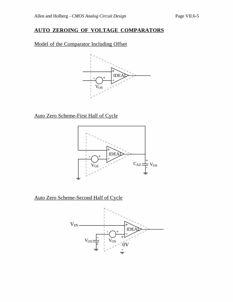
Allen and Holberg - CMOS Analog Circuit Design Page VII.6-5
AUTO ZEROING OF VOLTAGE COMPARATORS
Model of the Comparator Including Offset
IDEAL+
-+-
VOS
Auto Zero Scheme-First Half of Cycle
IDEAL+
-+-
VOS VOS+
-CAZ
Auto Zero Scheme-Second Half of Cycle
IDEAL+
-+-
VOSVOS+
-
VIN
+
-0V
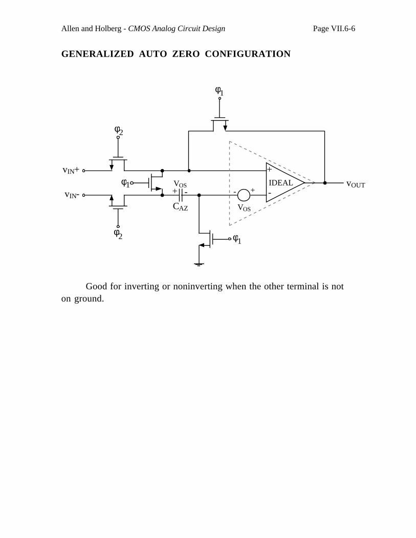
Allen and Holberg - CMOS Analog Circuit Design Page VII.6-6
GENERALIZED AUTO ZERO CONFIGURATION
IDEAL
+
-+-
VOS
vIN+
vIN-VOS
-+
CAZ
vOUTφ1
φ2
φ1
φ1
φ2
Good for inverting or noninverting when the other terminal is noton ground.
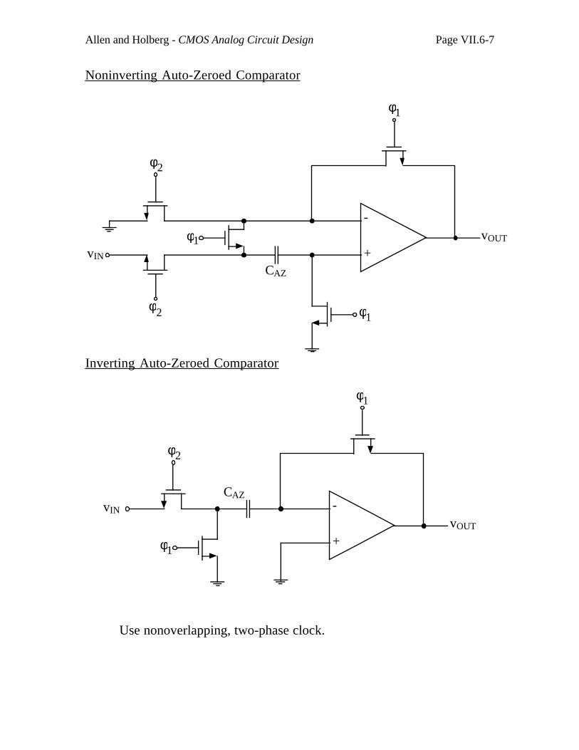
Allen and Holberg - CMOS Analog Circuit Design Page VII.6-7
Noninverting Auto-Zeroed Comparator
+
-
CAZ
vOUT
φ2
φ1
φ1
φ1
φ2
vIN
Inverting Auto-Zeroed Comparator
+
-CAZ
vOUT
φ2
φ1
φ1
vIN
Use nonoverlapping, two-phase clock.
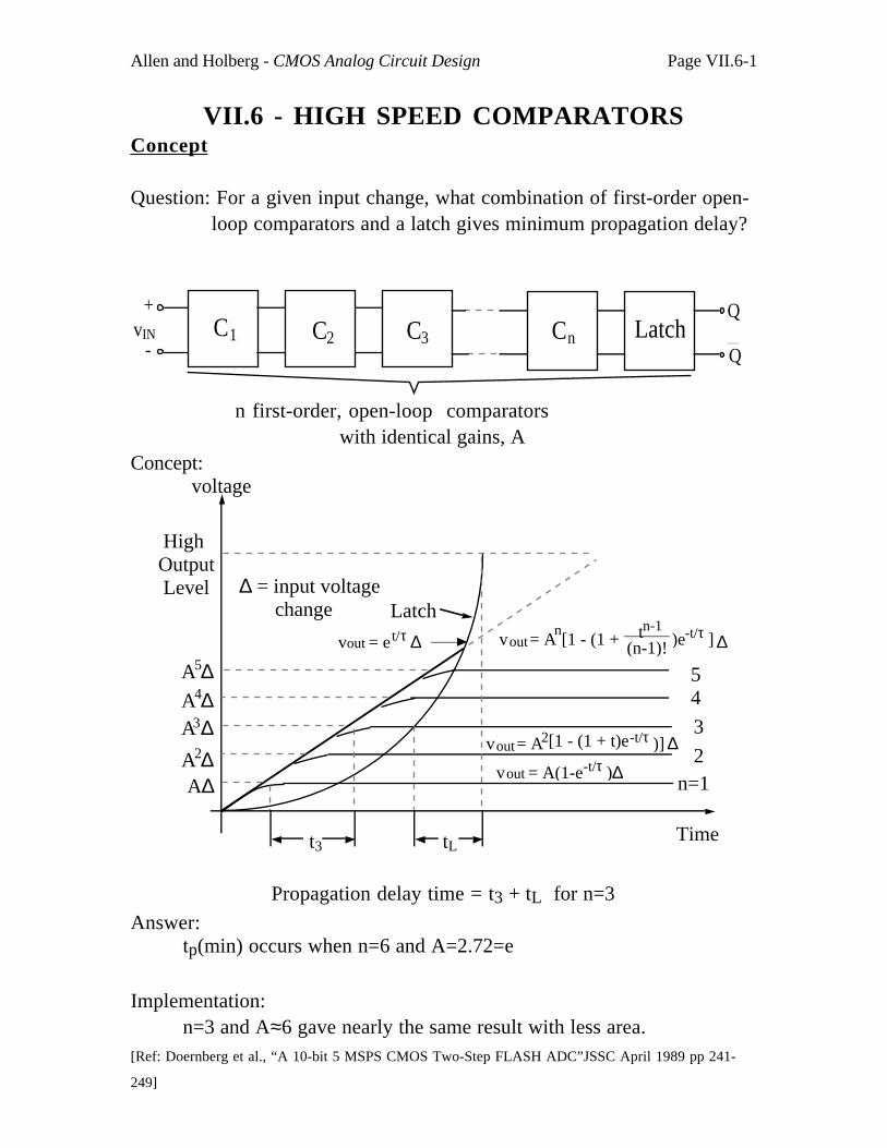
Allen and Holberg - CMOS Analog Circuit Design Page VII.6-1
VII.6 - HIGH SPEED COMPARATORS Concept
Question: For a given input change, what combination of first-order open- loop comparators and a latch gives minimum propagation delay?
C1
+
-C2 C3 Cn LatchvIN
Q
Q
n first-order, open-loop comparatorswith identical gains, A
Concept:voltage
HighOutput Level
tLt3
5
3
4
2n=1
Time
Latch
A ∆A∆
∆ = input voltage change
vout = A(1-e -t/τ )∆
vout= A -t/τ )] ∆2[1 - (1 + t)e
vout= A -t/τ ] ∆n[1 - (1 + (n-1)!
tn-1)evout = e t/τ ∆
2
A ∆3
A ∆4
A ∆5
Propagation delay time = t3 + tL for n=3
Answer:tp(min) occurs when n=6 and A=2.72=e
Implementation:n=3 and A≈6 gave nearly the same result with less area.
[Ref: Doernberg et al., “A 10-bit 5 MSPS CMOS Two-Step FLASH ADC”JSSC April 1989 pp 241-
249]

Allen and Holberg - CMOS Analog Circuit Design Page VII.6-2
HIGH SPEED COMPARATORS-CONT'D
Conceptual Implementation-
+
-vIN
Q
Q+
-
-
+
+
-
-
+
+
-
-
+Latch
FB
FB
Reset
VDD
VSS
VB1
VB2
Q
Q
LATCH
Offset and level shifting-
_
++
-
+ -vIN-VOS
VOS
vIN
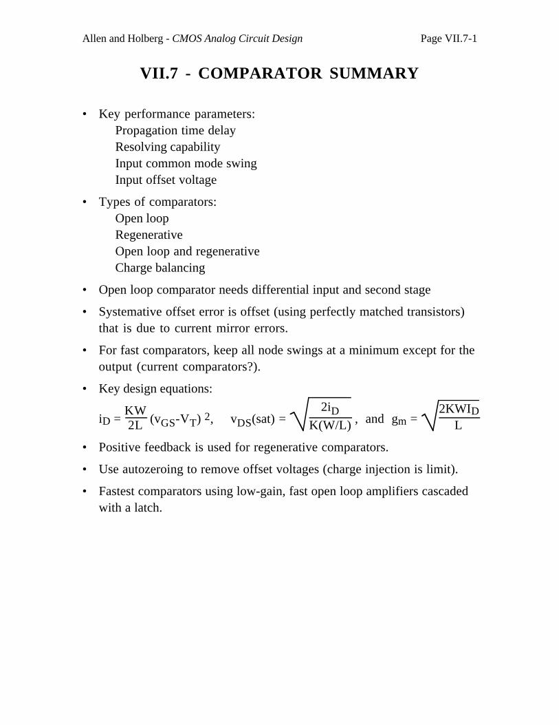
Allen and Holberg - CMOS Analog Circuit Design Page VII.7-1
VII.7 - COMPARATOR SUMMARY
• Key performance parameters:Propagation time delayResolving capabilityInput common mode swingInput offset voltage
• Types of comparators:Open loopRegenerativeOpen loop and regenerativeCharge balancing
• Open loop comparator needs differential input and second stage
• Systemative offset error is offset (using perfectly matched transistors)that is due to current mirror errors.
• For fast comparators, keep all node swings at a minimum except for theoutput (current comparators?).
• Key design equations:
iD = KW2L (vGS-VT) 2, vDS(sat) =
2iDK(W/L) , and gm =
2KWIDL
• Positive feedback is used for regenerative comparators.
• Use autozeroing to remove offset voltages (charge injection is limit).
• Fastest comparators using low-gain, fast open loop amplifiers cascadedwith a latch.
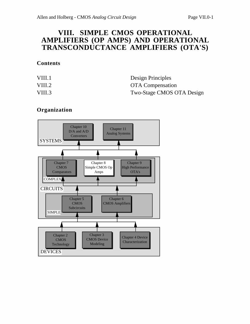
Allen and Holberg - CMOS Analog Circuit Design Page VII.0-1
VIII. SIMPLE CMOS OPERATIONALAMPLIFIERS (OP AMPS) AND OPERATIONALTRANSCONDUCTANCE AMPLIFIERS (OTA'S)
Contents
VIII.1 Design PrinciplesVIII.2 OTA CompensationVIII.3 Two-Stage CMOS OTA Design
Organization
DEVICES
SYSTEMS
CIRCUITS
Chapter 2 CMOS
Technology
Chapter 3 CMOS Device
Modeling
Chapter 4 Device Characterization
Chapter 7 CMOS
Comparators
Chapter 8 Simple CMOS Op
Amps
Chapter 9 High Performance
OTA's
Chapter 5 CMOS
Subcircuits
Chapter 6 CMOS Amplifiers
Chapter 10D/A and A/D
Converters
Chapter 11Analog Systems
SIMPLE
COMPLEX
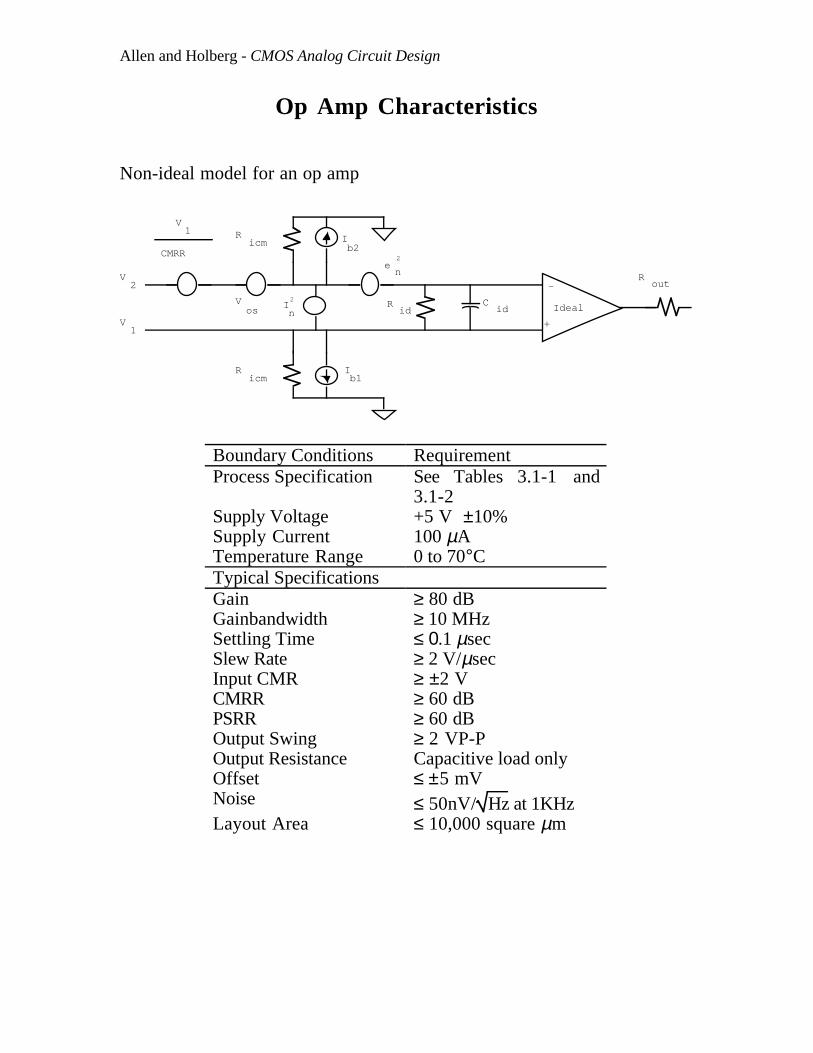
Allen and Holberg - CMOS Analog Circuit Design
Op Amp Characteristics
Non-ideal model for an op amp
b1I
b2I
Ricm
Ricm
CMRR
V1
CidR
idV1
V2
Ideal
+
-R
out
en
2
nI2V
os
Boundary Conditions RequirementProcess Specification See Tables 3.1-1 and
3.1-2Supply Voltage +5 V ±10%Supply Current 100 µATemperature Range 0 to 70°CTypical SpecificationsGain ≥ 80 dBGainbandwidth ≥ 10 MHzSettling Time ≤ 0.1 µsecSlew Rate ≥ 2 V/µsecInput CMR ≥ ±2 VCMRR ≥ 60 dBPSRR ≥ 60 dBOutput Swing ≥ 2 VP-POutput Resistance Capacitive load onlyOffset ≤ ±5 mVNoise ≤ 50nV/ Hz at 1KHzLayout Area ≤ 10,000 square µm
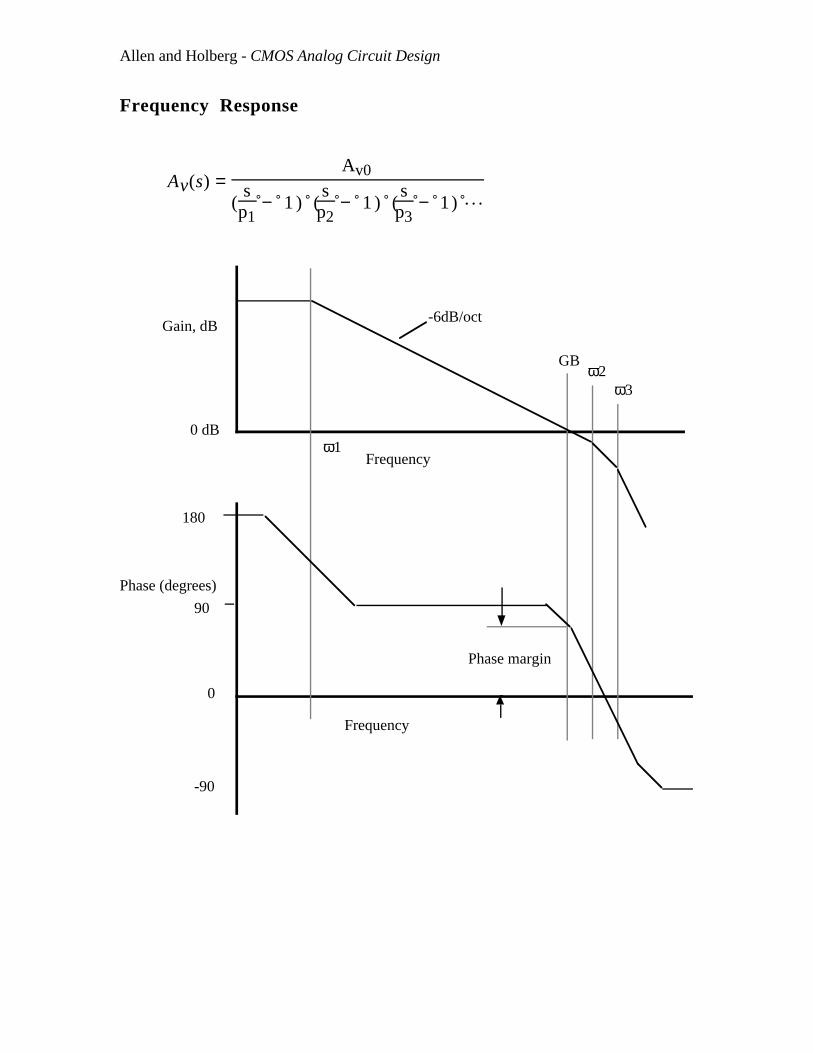
Allen and Holberg - CMOS Analog Circuit Design
Frequency Response
Av(s) = Av0
(s
p1 − 1 ) (
sp2
− 1 ) (s
p3 − 1) . . .
Gain, dB
Phase (degrees)
180
90
0
-6dB/oct
GBω2
ω3
ω1Frequency
Frequency
Phase margin
0 dB
-90
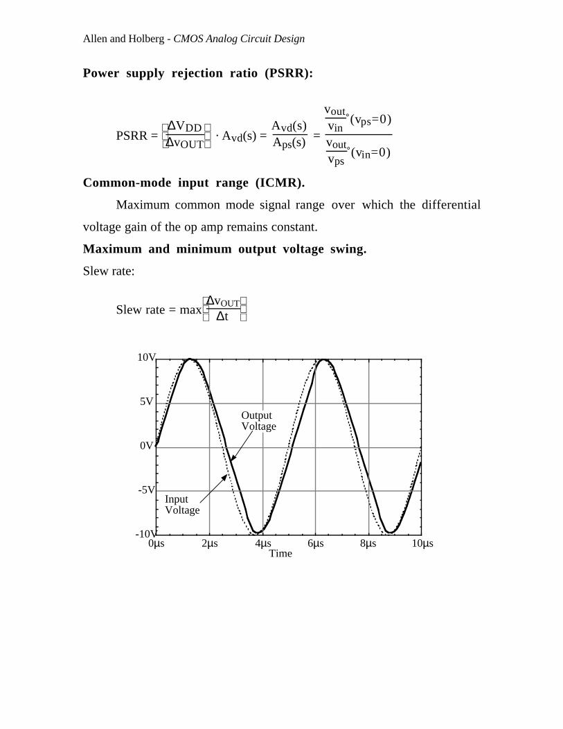
Allen and Holberg - CMOS Analog Circuit Design
Power supply rejection ratio (PSRR):
PSRR =
∆VDD
∆vOUT · Avd(s) =
Avd(s)Aps(s) =
voutvin
(vps=0)
voutvps
(vin=0)
Common-mode input range (ICMR).
Maximum common mode signal range over which the differential
voltage gain of the op amp remains constant.
Maximum and minimum output voltage swing.
Slew rate:
Slew rate = max
∆vOUT
∆t
-10V
-5V
0V
5V
10V
0µs 2µs 4µs 6µs 8µs 10µs
InputVoltage
OutputVoltage
Time
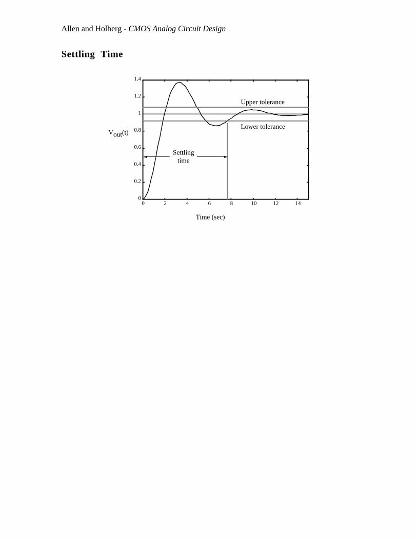
Allen and Holberg - CMOS Analog Circuit Design
Settling Time
0
0.2
0.4
0.6
0.8
1
1.2
1.4
0 2 4 6 8 10 12 14
Lower tolerance
Upper tolerance
Settling time
Time (sec)
Vout(t)
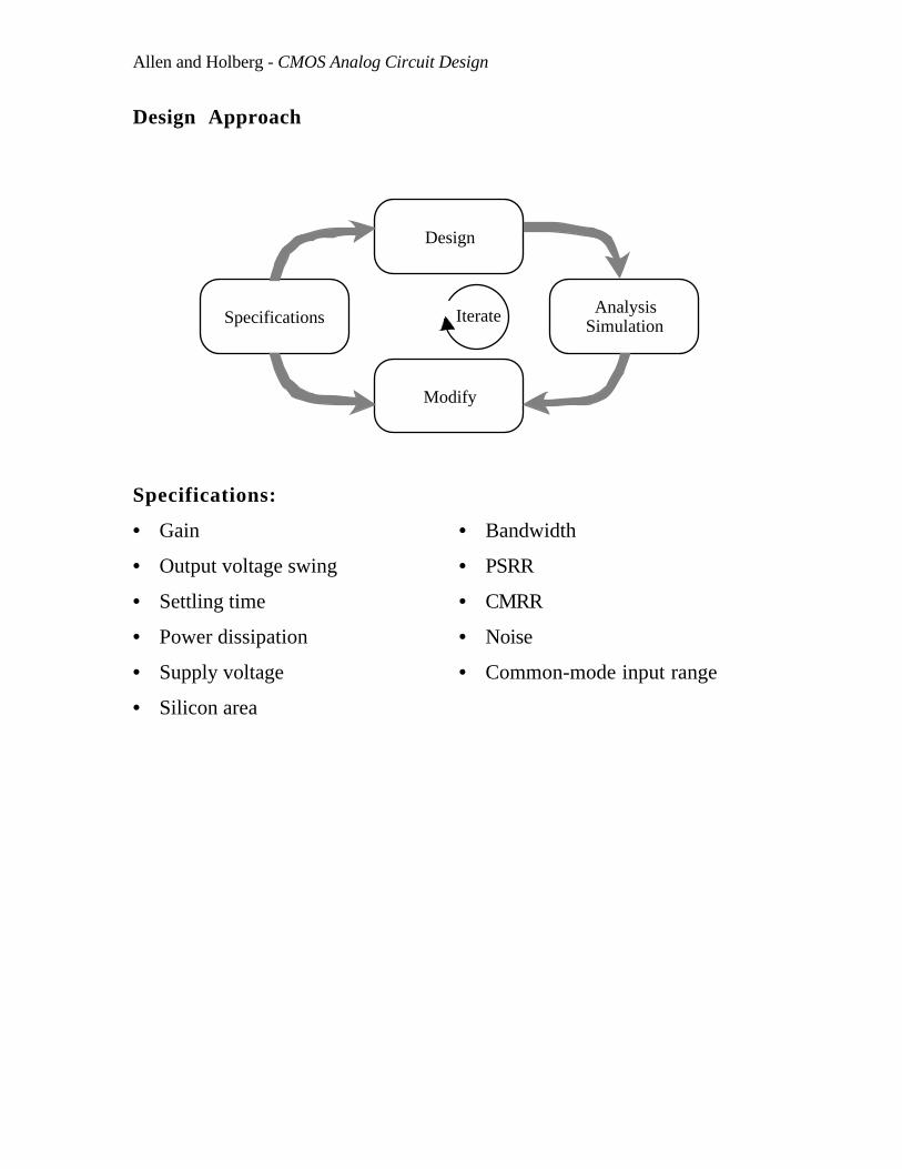
Allen and Holberg - CMOS Analog Circuit Design
Design Approach
SpecificationsAnalysis
Simulation
Modify
Design
Iterate
Specifications:
• Gain • Bandwidth
• Output voltage swing • PSRR
• Settling time • CMRR
• Power dissipation • Noise
• Supply voltage • Common-mode input range
• Silicon area

Allen and Holberg - CMOS Analog Circuit Design
Design Strategy
The design process involves two distinct activities:
Architecture Design
• Find an architecture already available and adapt it to present
requirements
• Create a new architecture that can meet requirements
Component Design
• Design transistor sizes
• Design compensation network
If available architectures do not meet requirements, then an existing
architecture must be modified, or a new one designed. Once a satisfactory
architecture has been obtained, then devices and the compensation network
must be designed.
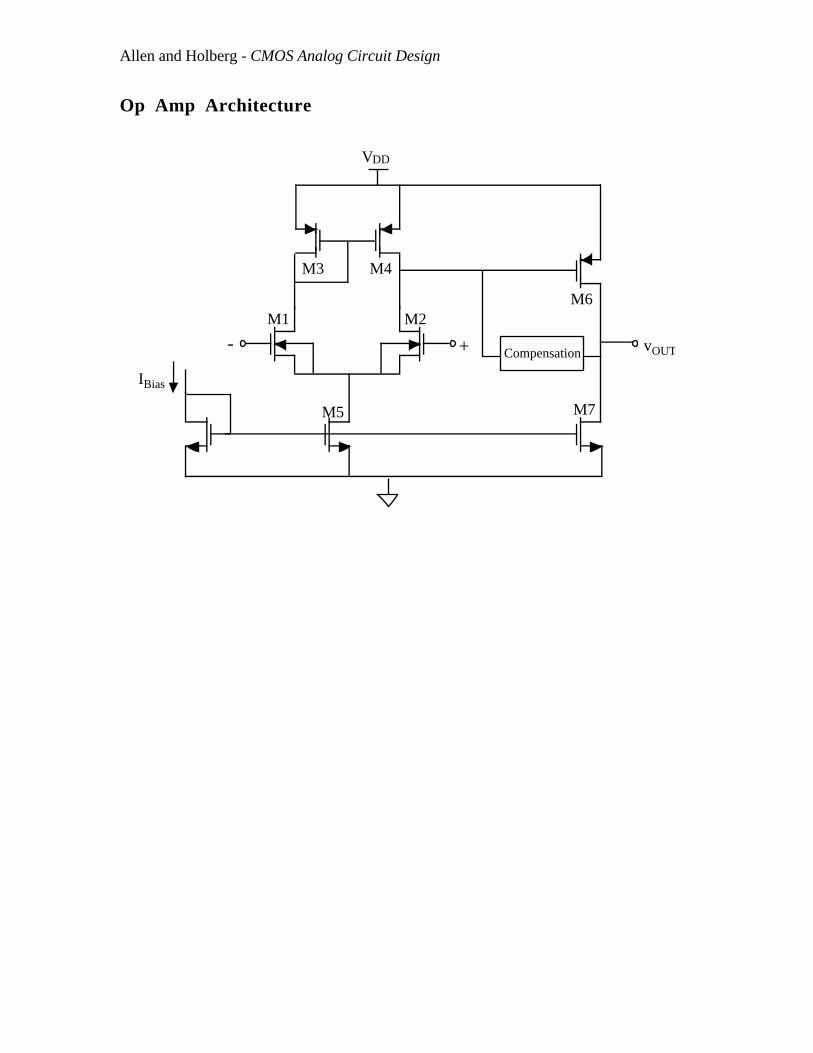
Allen and Holberg - CMOS Analog Circuit Design
Op Amp Architecture
M4M3
M1
+-M2
M5
M6
M7
IBias
VDD
vOUTCompensation
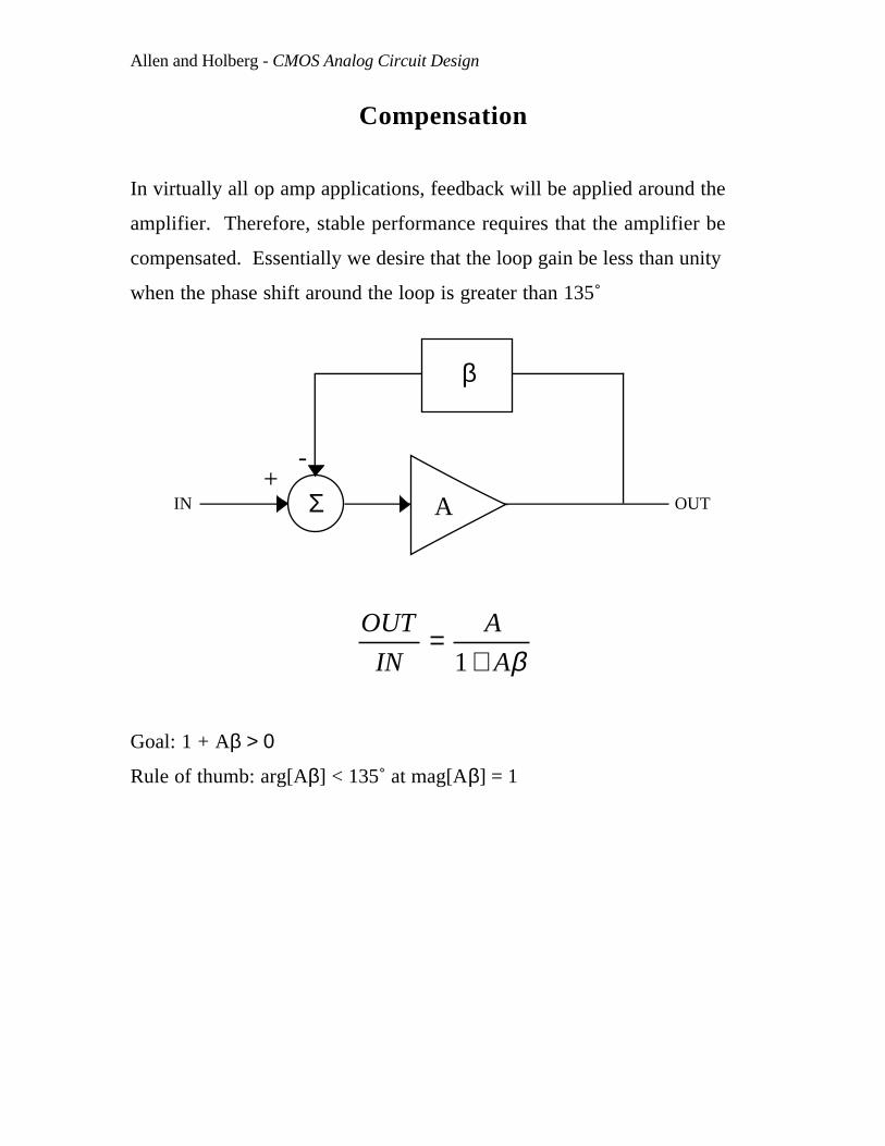
Allen and Holberg - CMOS Analog Circuit Design
Compensation
In virtually all op amp applications, feedback will be applied around the
amplifier. Therefore, stable performance requires that the amplifier be
compensated. Essentially we desire that the loop gain be less than unity
when the phase shift around the loop is greater than 135˚
Σ
β
A+
-
OUTIN
OUT
IN
A
A=
+1 β
Goal: 1 + Aβ > 0
Rule of thumb: arg[Aβ] < 135˚ at mag[Aβ] = 1
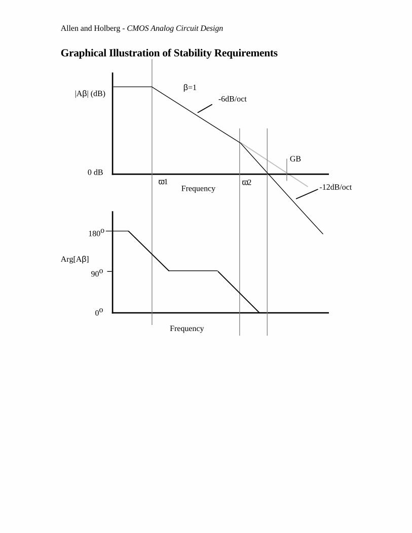
Allen and Holberg - CMOS Analog Circuit Design
Graphical Illustration of Stability Requirements
|Aβ| (dB)
180o
90o
0o
-6dB/oct
GB
ω2ω1Frequency
Frequency
-12dB/oct
Arg[Aβ]
β=1
0 dB
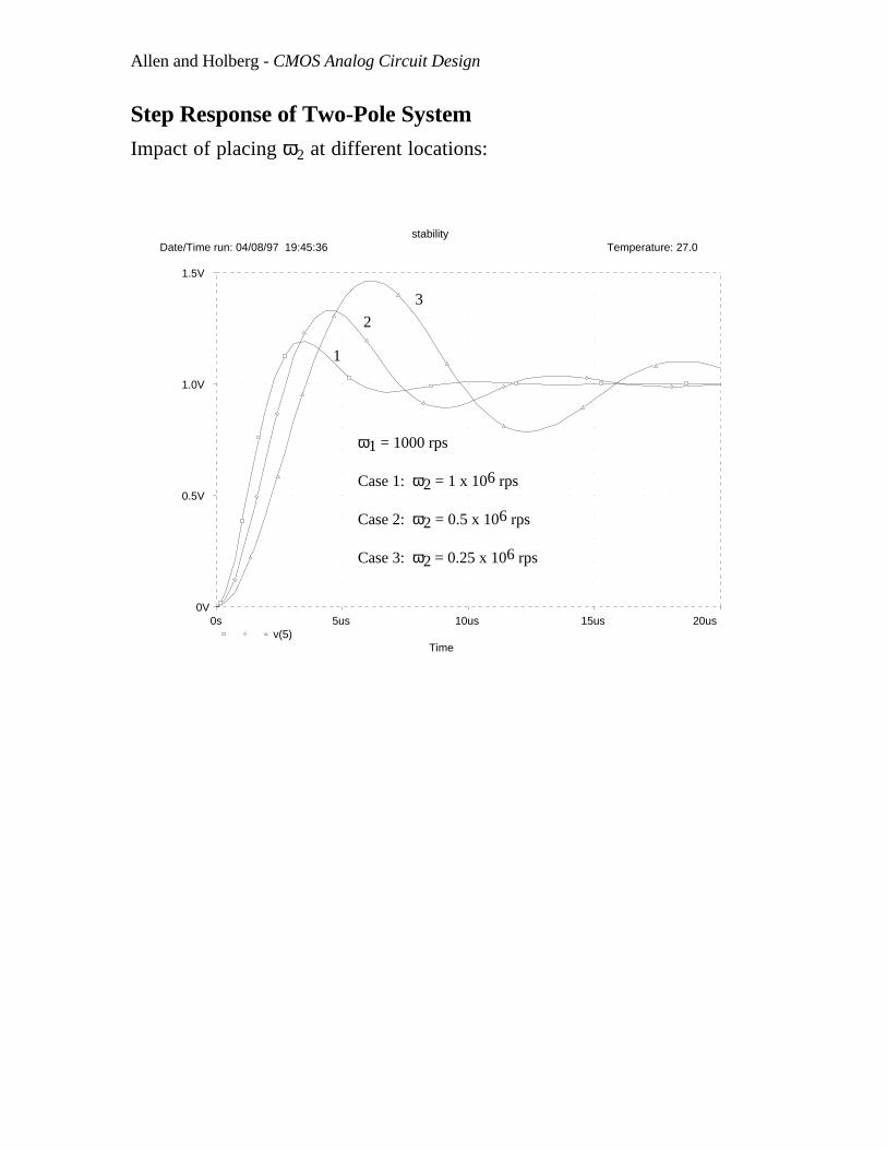
Allen and Holberg - CMOS Analog Circuit Design
Step Response of Two-Pole SystemImpact of placing ω2 at different locations:
0s 5us 10us 15us 20us
Timev(5)
1.5V
1.0V
0.5V
0V
stabilityDate/Time run: 04/08/97 19:45:36 Temperature: 27.0
ω1 = 1000 rps
Case 1: ω2 = 1 x 10⁶ rps
Case 2: ω2 = 0.5 x 10⁶ rps
Case 3: ω2 = 0.25 x 10⁶ rps
1
2
3
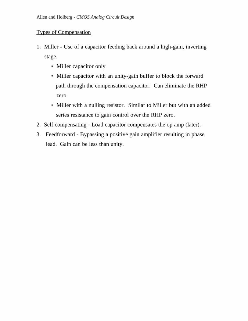
Allen and Holberg - CMOS Analog Circuit Design
Types of Compensation
1. Miller - Use of a capacitor feeding back around a high-gain, inverting
stage.
• Miller capacitor only
• Miller capacitor with an unity-gain buffer to block the forward
path through the compensation capacitor. Can eliminate the RHP
zero.
• Miller with a nulling resistor. Similar to Miller but with an added
series resistance to gain control over the RHP zero.
2. Self compensating - Load capacitor compensates the op amp (later).
3. Feedforward - Bypassing a positive gain amplifier resulting in phase
lead. Gain can be less than unity.
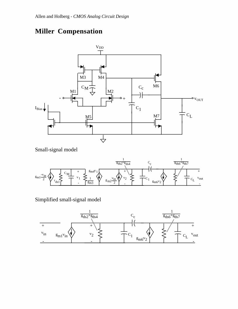
Allen and Holberg - CMOS Analog Circuit Design
Miller Compensation
M4M3
M1
+-M2
M5
M6
M7
IBias
VDD
vOUT
C1CL
CM Cc
Small-signal model
+
- -
+
CLC1
Cc
CMgm1 v1
gm3gm2
vin2
-vin2 rds1
1
gm4v1
v2
gds2+gds4
1
gm6v2
gds6+gds71
-
+
vout
Simplified small-signal model
-
+
CLC1
Cc
gm1vinv2
gds2+gds4
1
gm6v2
gds6+gds7
1
-
+
voutvin
-
+
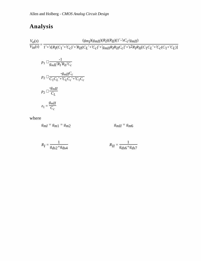
Allen and Holberg - CMOS Analog Circuit Design
Analysis
Vo(s)
Vin(s) = (gmI)(gmII)(RI)(RII)(1 - sCc/gmII)
1 + s[RI(C1 + Cc) + RII(CL + Cc) + gmIIRIRIICc] + s2RIRII[C1CL + Cc(C1+ CL)]
p1 ≅ -1
gmII RI RII Cc
p2 ≅ -gmIICc
C1CL + CLCc + C1Cc
p2 ≅ -gmIICL
z1 = gmIICc
wheregmI = gm1 = gm2 gmII = gm6
RI = 1
gds2+gds4RII =
1gds6+gds7
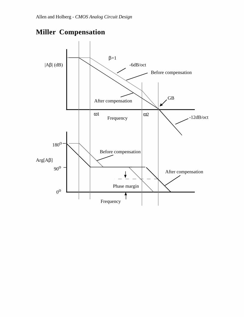
Allen and Holberg - CMOS Analog Circuit Design
Miller Compensation
Phase margin
180o
90o
0o
-6dB/oct
GB
ω2ω1Frequency
Frequency
-12dB/oct
Arg[Aβ]
β=1
Before compensation
After compensation
Before compensation
After compensation
|Aβ| (dB)
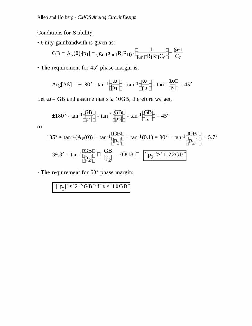
Allen and Holberg - CMOS Analog Circuit Design
Conditions for Stability
• Unity-gainbandwith is given as:
GB = Av(0)·|p1| = ( )gmIgmIIRIRII ·
1
gmIIRIRIICc =
gmICc
• The requirement for 45° phase margin is:
Arg[Aß] = ±180° - tan-1
ω
|p1| - tan-1
ω
|p2| - tan-1
ω
z = 45°
Let ω = GB and assume that z ≥ 10GB, therefore we get,
±180° - tan-1
GB
|p1| - tan-1
GB
|p2| - tan-1
GB
z = 45°
or
135° ≈ tan-1(Av(0)) + tan-1
GB
|p2| + tan-1(0.1) = 90° + tan-1
GB
|p2 | + 5.7°
39.3° ≈ tan-1
GB
|p2| ⇒ GB|p2| = 0.818 ⇒ |p2| ≥ 1.22GB
• The requirement for 60° phase margin:
| p2 | ≥ 2.2GB if z ≥ 10GB

Allen and Holberg - CMOS Analog Circuit Design
• If 60° phase margin is required, then the following relationships apply:
gmIICc
> 10gmI
Cc ⇒ gm II > 10gm I
Furthermore,gmIIC2
> 2.2gmI
Cc
which after substitution gives:
Cc > 0.22C2
Note:gmI = gm1 = gm2 and gmII = gm6
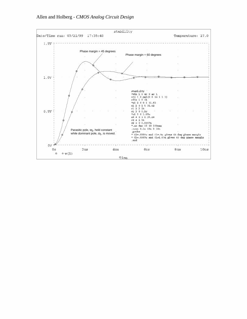
Allen and Holberg - CMOS Analog Circuit Design
Phase margin = 45 degreesPhase margin = 60 degrees
Parasitic pole, ω2, held constantwhile dominant pole, ω1, is moved.
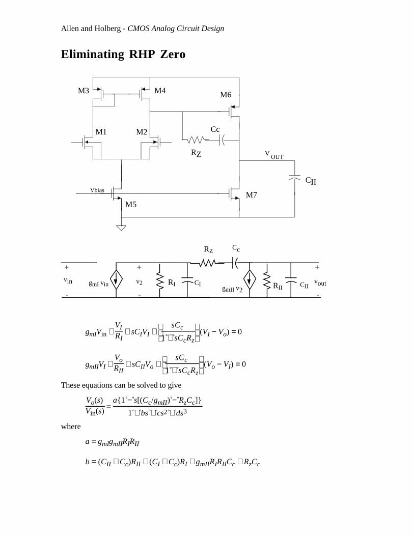
Allen and Holberg - CMOS Analog Circuit Design
Eliminating RHP Zero
V OUT
M7
M1 M2
M3 M4
M5
M6
Vbias
Cc
CII
-
+
CIICI
Cc
gmI vin v2gmII v2
-
+
voutvin
-
+
RI RII
RZ
RZ
gmIVin + VIRI
+ sCIVI +
sCc
1 + sCcRz (VI − Vo) = 0
gmIIVI + VoRII
+ sCIIVo +
sCc
1 + sCcRz (Vo − VI) = 0
These equations can be solved to give
Vo(s)Vin(s) =
a1 − s[(Cc/gmII) − RzCc]
1 + bs + cs2 + ds3
where
a = gmIgmIIRIRII
b = (CII + Cc)RII + (CI + Cc)RI + gmIIRIRIICc + RzCc

Allen and Holberg - CMOS Analog Circuit Design
c = [RIRII(CICII + CcCI + CcCII) + RzCc(RICI + RIICII)]
d = RIRIIRzCICIICc
If Rz is assumed to be less than RI or RII and the poles widely spaced, then the roots are
p1 ≅ −1
(1 + gmIIRII)RICc ≅
−1gmIIRIIRICc
p2 ≅ −gmIICc
CICII + CcCI + CcCII ≅
−gmIICII
p3 = −1
RzCI
and
z1 = 1
Cc(1/gmII − Rz)
By setting
Rz = 1/gmII
The RHP zero moves to infinity
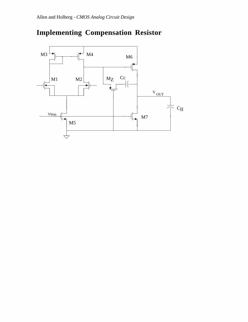
Allen and Holberg - CMOS Analog Circuit Design
Implementing Compensation Resistor
V OUT
M7
M1 M2
M3 M4
M5
M6
Vbias
Cc
CII
MZ
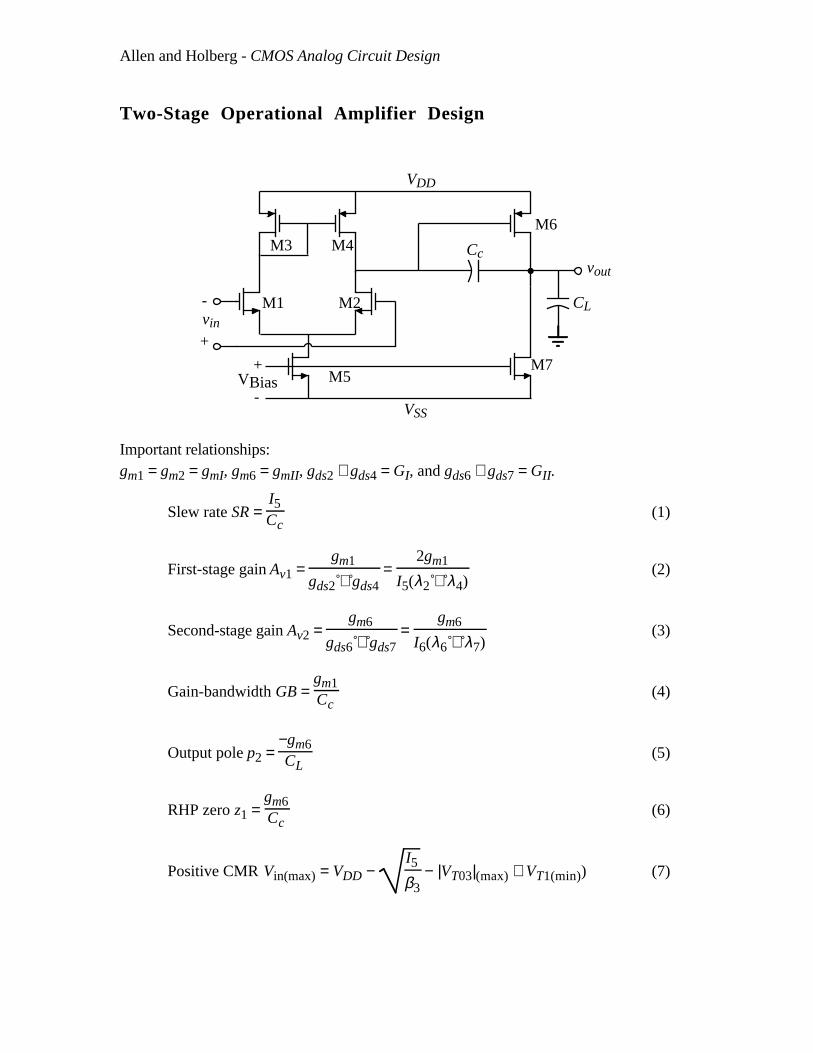
Allen and Holberg - CMOS Analog Circuit Design
Two-Stage Operational Amplifier Design
-
+
vin
M1 M2
M3 M4
M5
M6
M7
vout
VDD
VSS
VBias+
-
Cc
CL
Figure 6.3-1 Schematic of an unbuffered, two-stage CMOS op amp with an n-channel input pair.Important relationships:
gm1 = gm2 = gmI, gm6 = gmII, gds2 + gds4 = GI, and gds6 + gds7 = GII.
Slew rate SR = I5Cc
(1)
First-stage gain Av1 = gm1
gds2 + gds4 =
2gm1
I5(λ2 + λ4)(2)
Second-stage gain Av2 = gm6
gds6 + gds7 =
gm6
I6(λ6 + λ7)(3)
Gain-bandwidth GB = gm1Cc
(4)
Output pole p2 = −gm6CL
(5)
RHP zero z1 = gm6Cc
(6)
Positive CMR Vin(max) = VDD − I5
β3 − |VT03|(max) + VT1(min)) (7)
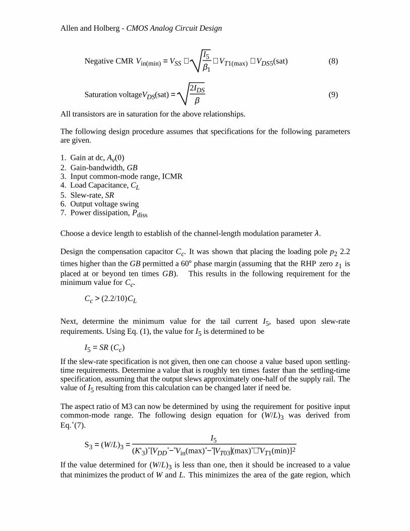
Allen and Holberg - CMOS Analog Circuit Design
Negative CMR Vin(min) = VSS + I5
β1 + VT1(max) + VDS5(sat) (8)
Saturation voltageVDS(sat) = 2IDS
β(9)
All transistors are in saturation for the above relationships.
The following design procedure assumes that specifications for the following parametersare given.
1. Gain at dc, Av(0)2. Gain-bandwidth, GB3. Input common-mode range, ICMR4. Load Capacitance, CL5. Slew-rate, SR6. Output voltage swing7. Power dissipation, Pdiss
Choose a device length to establish of the channel-length modulation parameter λ.
Design the compensation capacitor Cc. It was shown that placing the loading pole p2 2.2
times higher than the GB permitted a 60° phase margin (assuming that the RHP zero z1 isplaced at or beyond ten times GB). This results in the following requirement for theminimum value for Cc.
Cc > (2.2/10)CL
Next, determine the minimum value for the tail current I5, based upon slew-raterequirements. Using Eq. (1), the value for I5 is determined to be
I5 = SR (Cc)
If the slew-rate specification is not given, then one can choose a value based upon settling-time requirements. Determine a value that is roughly ten times faster than the settling-timespecification, assuming that the output slews approximately one-half of the supply rail. Thevalue of I5 resulting from this calculation can be changed later if need be.
The aspect ratio of M3 can now be determined by using the requirement for positive inputcommon-mode range. The following design equation for (W/L)3 was derived fromEq. (7).
S3 = (W/L)3 = I5
(K'3) [VDD − Vin(max) − |VT03|(max) + VT1(min)]2
If the value determined for (W/L)3 is less than one, then it should be increased to a valuethat minimizes the product of W and L. This minimizes the area of the gate region, which
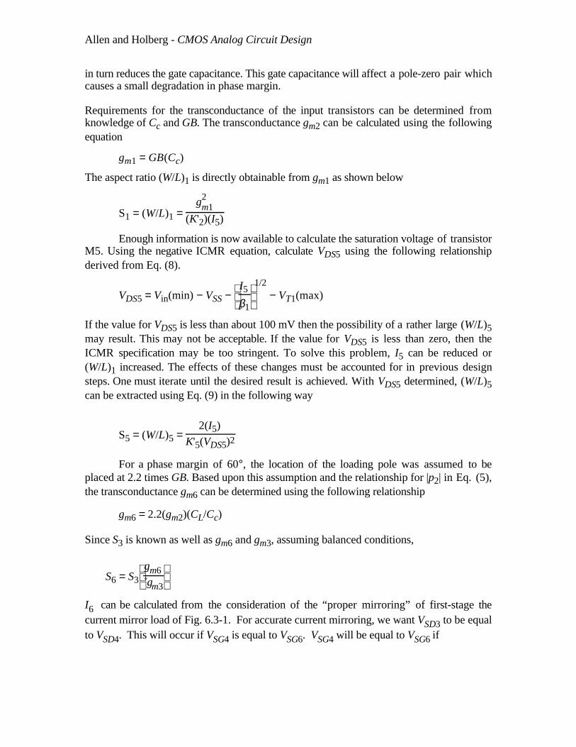
Allen and Holberg - CMOS Analog Circuit Design
in turn reduces the gate capacitance. This gate capacitance will affect a pole-zero pair whichcauses a small degradation in phase margin.
Requirements for the transconductance of the input transistors can be determined fromknowledge of Cc and GB. The transconductance gm2 can be calculated using the followingequation
gm1 = GB(Cc)
The aspect ratio (W/L)1 is directly obtainable from gm1 as shown below
S1 = (W/L)1 = g2
m1(K'2)(I5)
Enough information is now available to calculate the saturation voltage of transistorM5. Using the negative ICMR equation, calculate VDS5 using the following relationshipderived from Eq. (8).
VDS5 = Vin(min) − VSS −
I5
β1
1/2
− VT1(max)
If the value for VDS5 is less than about 100 mV then the possibility of a rather large (W/L)5may result. This may not be acceptable. If the value for VDS5 is less than zero, then theICMR specification may be too stringent. To solve this problem, I5 can be reduced or(W/L)1 increased. The effects of these changes must be accounted for in previous designsteps. One must iterate until the desired result is achieved. With VDS5 determined, (W/L)5can be extracted using Eq. (9) in the following way
S5 = (W/L)5 = 2(I5)
K'5(VDS5)2
For a phase margin of 60°, the location of the loading pole was assumed to beplaced at 2.2 times GB. Based upon this assumption and the relationship for |p2| in Eq. (5),the transconductance gm6 can be determined using the following relationship
gm6 = 2.2(gm2)(CL/Cc)
Since S3 is known as well as gm6 and gm3, assuming balanced conditions,
S6 = S3
gm6
gm3
I6 can be calculated from the consideration of the “proper mirroring” of first-stage thecurrent mirror load of Fig. 6.3-1. For accurate current mirroring, we want VSD3 to be equalto VSD4. This will occur if VSG4 is equal to VSG6. VSG4 will be equal to VSG6 if

Allen and Holberg - CMOS Analog Circuit Design
I6 = (W/L)6(W/L)4
I1 =
S6
S4 I1
Choose the larger of these two values for I6 (Eq. 19 or Eq. 20). If the larger value is foundin Eq (19), then (W/L)6 must be increased to satisfy Eq. (20). If the larger value is found inEq. (20), then no other adjustments must be made. One also should check the powerdissipation requirements since I6 will most likely determine the majority of the powerdissipation.
The device size of M7 can be determined from the balance equation given below
S7 = (W/L)7 = (W/L)5
I6
I5 = S5
I6
I5
The first-cut design of all W/L ratios are now complete. Fig. 6.3-2 illustrates the abovedesign procedure showing the various design relationships and where they apply in thetwo-stage CMOS op amp.
-
+
vin M1 M2
M3 M4
M5
M6
M7
vout
VDD
VSS
VBias+
-
Cc
CL
VSG4+
-
Max. ICMRand/or p3
VSG6+
-
Vout(max)
I6
gm6 or Proper Mirroring
VSG4=VSG6
Cc ≈ 0.2CL(PM = 60°)
GB =gm1Cc
Min. ICMR I5 I5 = SR·Cc Vout(min)
Figure 6.3-2 Illustration of the design relationships and the circuit fora two-stage CMOS op amp.
At this point in the design procedure, the total amplifier gain must be checked against thespecifications.
Av = (2)(gm2)(gm6)
I5(λ2 + λ3)I6(λ6 + λ7)
If the gain is too low, a number of things can be adjusted. The best way to do this is to usethe table below, which shows the effects of various device sizes and currents on the
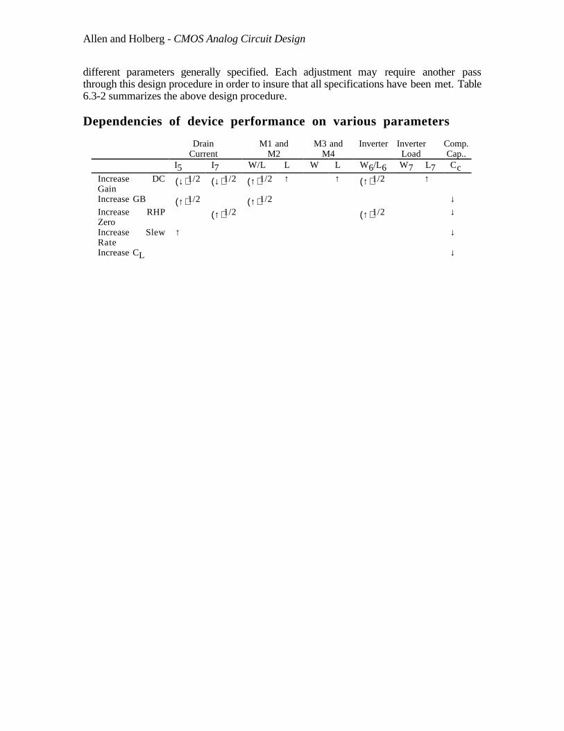
Allen and Holberg - CMOS Analog Circuit Design
different parameters generally specified. Each adjustment may require another passthrough this design procedure in order to insure that all specifications have been met. Table6.3-2 summarizes the above design procedure.
Dependencies of device performance on various parameters
Drain M1 and M3 and Inverter Inverter Comp.Current M2 M4 Load Cap..
I5 I7 W/L L W L W6/L6 W7 L7 CcIncrease DCGain
(↓)1/2 (↓)1/2 (↑)1/2 ↑ ↑ (↑)1/2 ↑
Increase GB (↑)1/2 (↑)1/2 ↓Increase RHPZero
(↑)1/2 (↑)1/2 ↓
Increase SlewRate
↑ ↓
Increase CL ↓
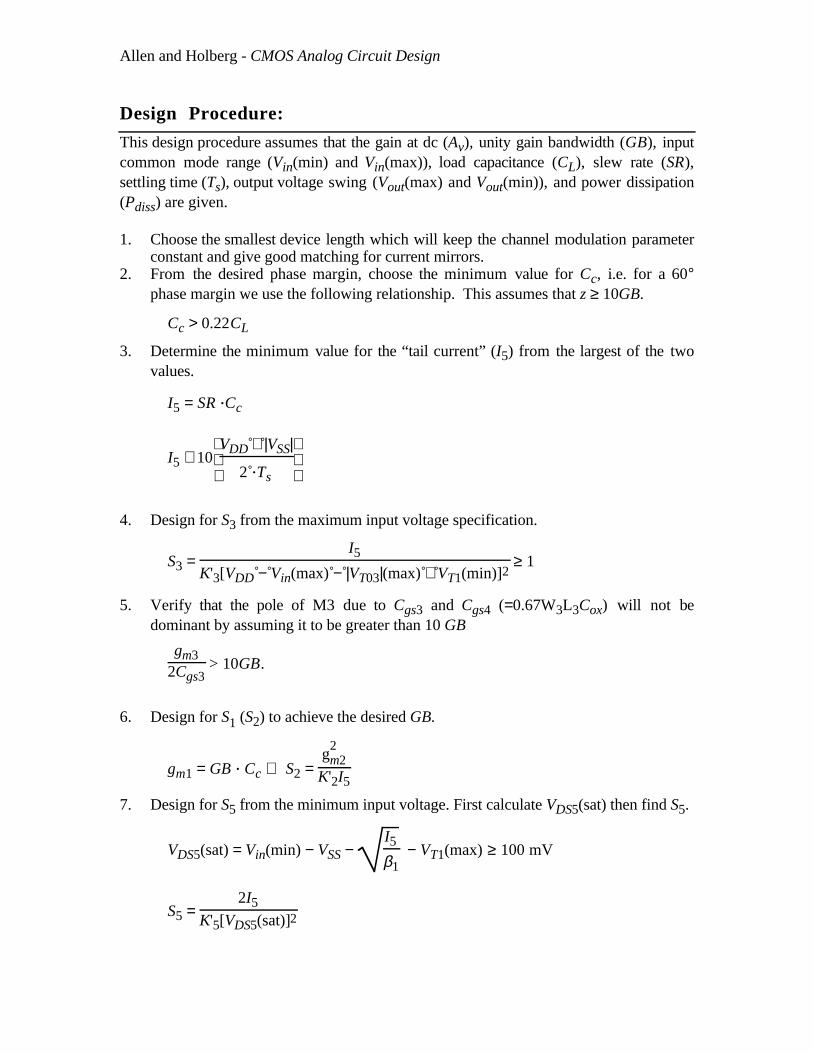
Allen and Holberg - CMOS Analog Circuit Design
Design Procedure:
This design procedure assumes that the gain at dc (Av), unity gain bandwidth (GB), inputcommon mode range (Vin(min) and Vin(max)), load capacitance (CL), slew rate (SR),settling time (Ts), output voltage swing (Vout(max) and Vout(min)), and power dissipation(Pdiss) are given.
1. Choose the smallest device length which will keep the channel modulation parameterconstant and give good matching for current mirrors.
2. From the desired phase margin, choose the minimum value for Cc, i.e. for a 60°phase margin we use the following relationship. This assumes that z ≥ 10GB.
Cc > 0.22CL
3. Determine the minimum value for the “tail current” (I5) from the largest of the twovalues.
I5 = SR .Cc
I5 ≅ 10
VDD + |VSS|
2 .Ts
4. Design for S3 from the maximum input voltage specification.
S3 = I5
K'3[VDD − Vin(max) − |VT03|(max) + VT1(min)]2 ≥ 1
5. Verify that the pole of M3 due to Cgs3 and Cgs4 (=0.67W3L3Cox) will not bedominant by assuming it to be greater than 10 GB
gm32Cgs3
> 10GB.
6. Design for S1 (S2) to achieve the desired GB.
gm1 = GB . Cc ⇒ S2 = g
2m2
K'2I5
7. Design for S5 from the minimum input voltage. First calculate VDS5(sat) then find S5.
VDS5(sat) = Vin(min) − VSS − I5
β1 − VT1(max) ≥ 100 mV
S5 = 2I5
K'5[VDS5(sat)]2
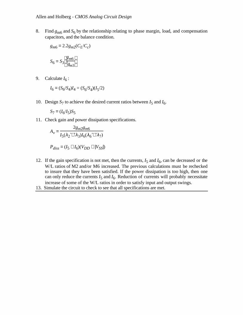
Allen and Holberg - CMOS Analog Circuit Design
8. Find gm6 and S6 by the relationship relating to phase margin, load, and compensationcapacitors, and the balance condition.
gm6 = 2.2gm2(CL/Cc)
S6 = S3
gm6
gm3
9. Calculate I6 :
I6 = (S6/S4)I4 = (S6/S4)(I5/2)
10. Design S7 to achieve the desired current ratios between I5 and I6.
S7 = (I6/I5)S5
11. Check gain and power dissipation specifications.
Av = 2gm2gm6
I5(λ2 + λ3)I6(λ6 + λ7)
Pdiss = (I5 + I6)(VDD + |VSS|)
12. If the gain specification is not met, then the currents, I5 and I6, can be decreased or theW/L ratios of M2 and/or M6 increased. The previous calculations must be recheckedto insure that they have been satisfied. If the power dissipation is too high, then onecan only reduce the currents I5 and I6. Reduction of currents will probably necessitateincrease of some of the W/L ratios in order to satisfy input and output swings.
13. Simulate the circuit to check to see that all specifications are met.
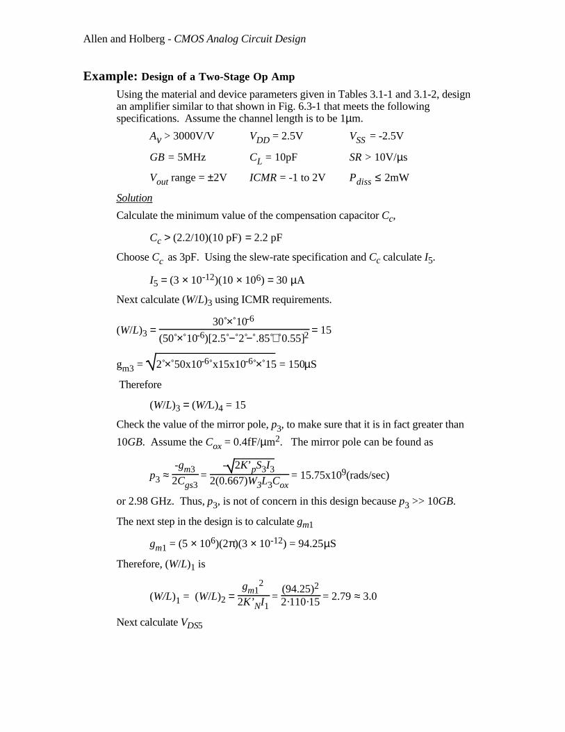
Allen and Holberg - CMOS Analog Circuit Design
Example: Design of a Two-Stage Op Amp
Using the material and device parameters given in Tables 3.1-1 and 3.1-2, designan amplifier similar to that shown in Fig. 6.3-1 that meets the followingspecifications. Assume the channel length is to be 1µm.
Av > 3000V/V VDD = 2.5V VSS = -2.5V
GB = 5MHz CL = 10pF SR > 10V/µs
Vout range = ±2V ICMR = -1 to 2V Pdiss ≤ 2mW
Solution
Calculate the minimum value of the compensation capacitor Cc,
Cc > (2.2/10)(10 pF) = 2.2 pF
Choose Cc as 3pF. Using the slew-rate specification and Cc calculate I5.
I5 = (3 × 10-12)(10 × 106) = 30 µA
Next calculate (W/L)3 using ICMR requirements.
(W/L)3 = 30 × 10-6
(50 × 10-6)[2.5 − 2 − .85 + 0.55]2 = 15
gm3 = 2 × 50x10-6 x15x10-6 × 15 = 150µS
Therefore
(W/L)3 = (W/L)4 = 15
Check the value of the mirror pole, p3, to make sure that it is in fact greater than
10GB. Assume the Cox = 0.4fF/µm2. The mirror pole can be found as
p3 ≈ -gm32Cgs3
= - 2K’pS3I3
2(0.667)W3L3Cox = 15.75x10⁹(rads/sec)
or 2.98 GHz. Thus, p3, is not of concern in this design because p3 >> 10GB.
The next step in the design is to calculate gm1
gm1 = (5 × 10⁶)(2π)(3 × 10-12) = 94.25µS
Therefore, (W/L)1 is
(W/L)1 = (W/L)2 = gm1
2
2K’NI1 =
(94.25)2
2·110·15 = 2.79 ≈ 3.0
Next calculate VDS5
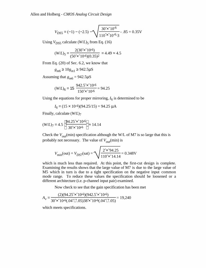
Allen and Holberg - CMOS Analog Circuit Design
VDS5 = (−1) − (−2.5) −30 × 10-6
110 × 10-6·3 - .85 = 0.35V
Using VDS5 calculate (W/L)5 from Eq. (16)
(W/L)5 = 2(30 × 10-6)
(50 × 10-6)(0.35)2 = 4.49 ≈ 4.5
From Eq. (20) of Sec. 6.2, we know that
gm6 ≥ 10gm1 ≥ 942.5µS
Assuming that gm6 = 942.5µS
(W/L)6 = 15 942.5 × 10⁻⁶
150 × 10-6 = 94.25
Using the equations for proper mirroring, I6 is determined to be
I6 = (15 × 10-6)(94.25/15) = 94.25 µA
Finally, calculate (W/L)7
(W/L)7 = 4.5
94.25 × 10⁻⁶
30 × 10-6 ≈ 14.14
Check the Vout(min) specification although the W/L of M7 is so large that this isprobably not necessary. The value of Vout(min) is
Vmin(out) = VDS7(sat) = 2 × 94.25
110 × 14.14 = 0.348V
which is much less than required. At this point, the first-cut design is complete.Examining the results shows that the large value of M7 is due to the large value ofM5 which in turn is due to a tight specification on the negative input commonmode range. To reduce these values the specification should be loosened or adifferent architecture (i.e. p-channel input pair) examined.
Now check to see that the gain specification has been met
Av = (2)(94.25 × 10⁻⁶)(942.5 × 10⁻⁶)
30 × 10-6(.04 + .05)38 × 10-6(.04 + .05) = 19,240
which meets specifications.
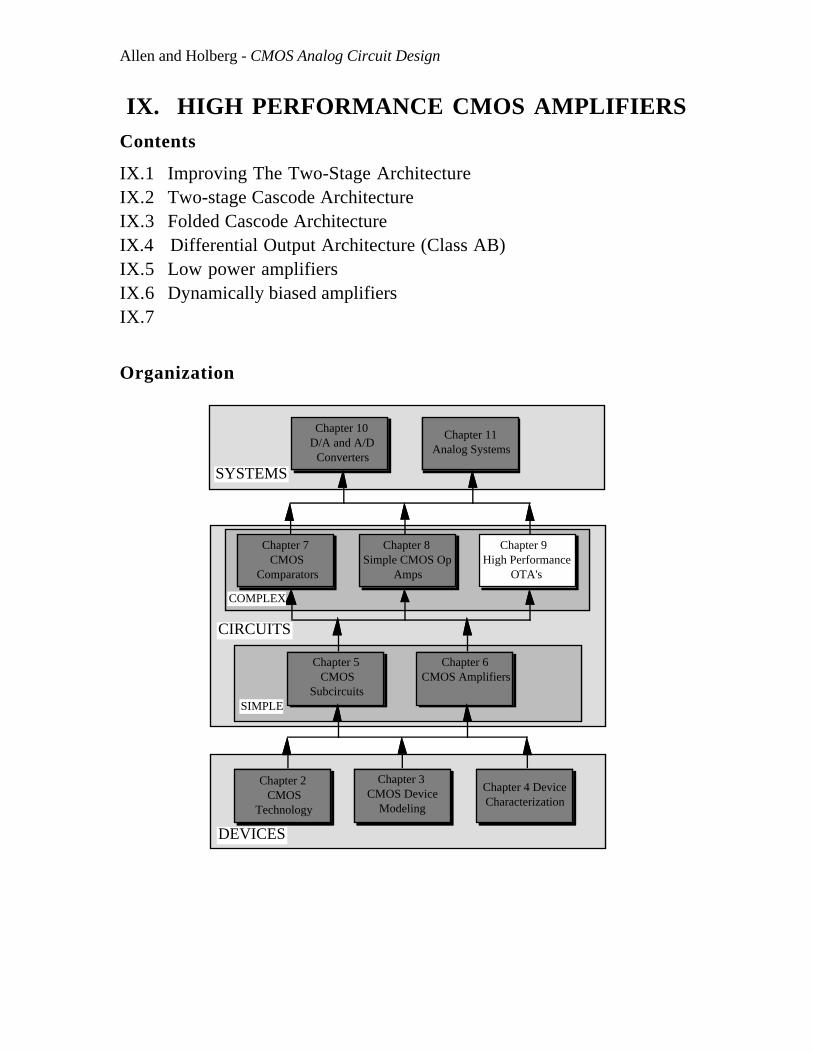
Allen and Holberg - CMOS Analog Circuit Design
IX. HIGH PERFORMANCE CMOS AMPLIFIERSContents
IX.1 Improving The Two-Stage ArchitectureIX.2 Two-stage Cascode ArchitectureIX.3 Folded Cascode ArchitectureIX.4 Differential Output Architecture (Class AB)IX.5 Low power amplifiersIX.6 Dynamically biased amplifiersIX.7
Organization
DEVICES
SYSTEMS
CIRCUITS
Chapter 2 CMOS
Technology
Chapter 3 CMOS Device
Modeling
Chapter 4 Device Characterization
Chapter 7 CMOS
Comparators
Chapter 8 Simple CMOS Op
Amps
Chapter 9 High Performance
OTA's
Chapter 5 CMOS
Subcircuits
Chapter 6 CMOS Amplifiers
Chapter 10D/A and A/D
Converters
Chapter 11Analog Systems
SIMPLE
COMPLEX
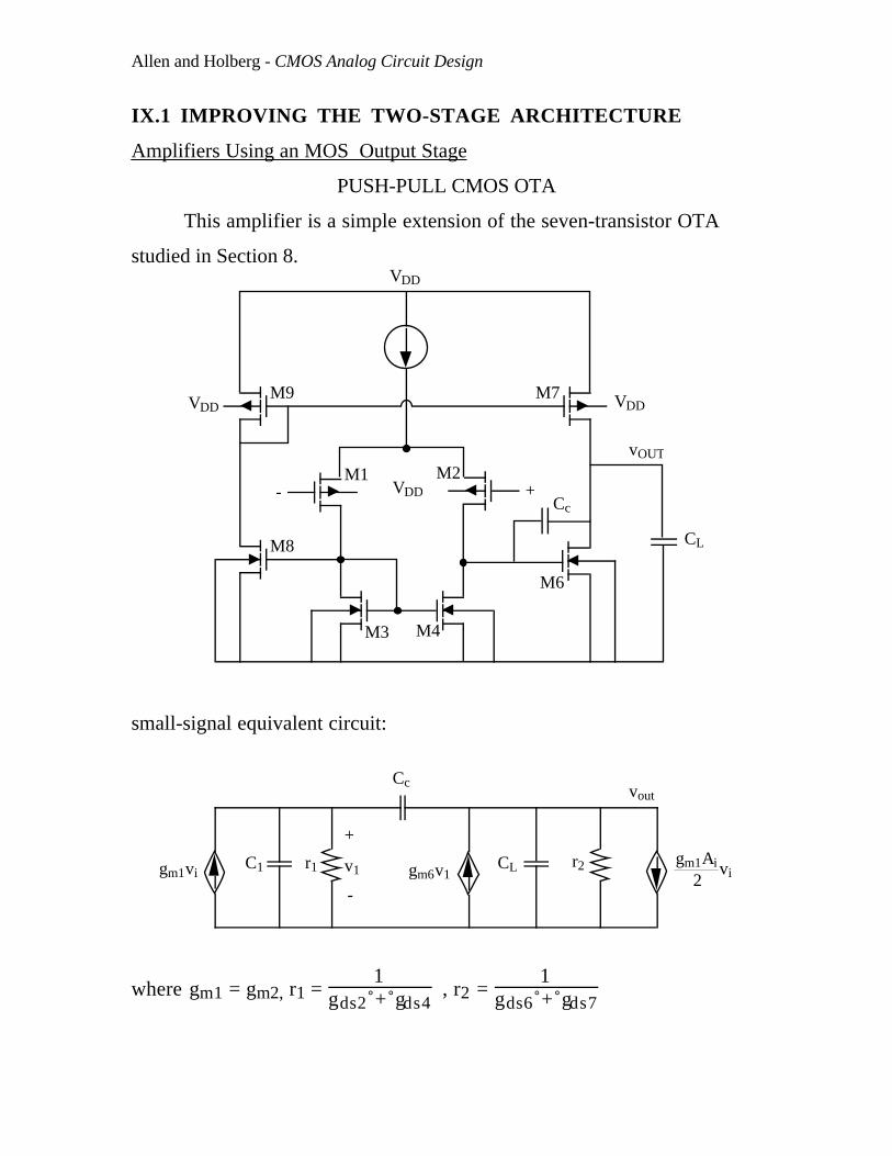
Allen and Holberg - CMOS Analog Circuit Design
IX.1 IMPROVING THE TWO-STAGE ARCHITECTURE
Amplifiers Using an MOS Output Stage
PUSH-PULL CMOS OTA
This amplifier is a simple extension of the seven-transistor OTA
studied in Section 8.
M1 M2
M9 M7
M8
M3 M4
M6
VDD
VDD VDD
CL
Cc+-
vOUT
VDD
small-signal equivalent circuit:
gm1vi gm6v1
+
-
v1r1C1
Cc
CL r2
vout
gm1Ai
2vi
where gm1 = gm2, r1 = 1
gds2 + gds4 , r2 =
1gds6 + gds7
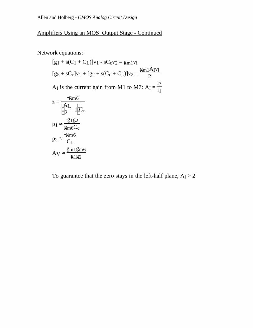
Allen and Holberg - CMOS Analog Circuit Design
Amplifiers Using an MOS Output Stage - Continued
Network equations:
[g1 + s(C1 + CL)]v1 - sCcv2 = gm1vi
[g5 + sCc]v1 + [g2 + s(Cc + CL)]v2 = gm1AIvi
2
AI is the current gain from M1 to M7: AI = i7i1
z = -gm6
AI
2 - 1 Cc
p1 ≈ -g1g2gm6Cc
p2 ≈ -gm6CL
AV ≈ gm1gm6
g1g2
To guarantee that the zero stays in the left-half plane, AI > 2
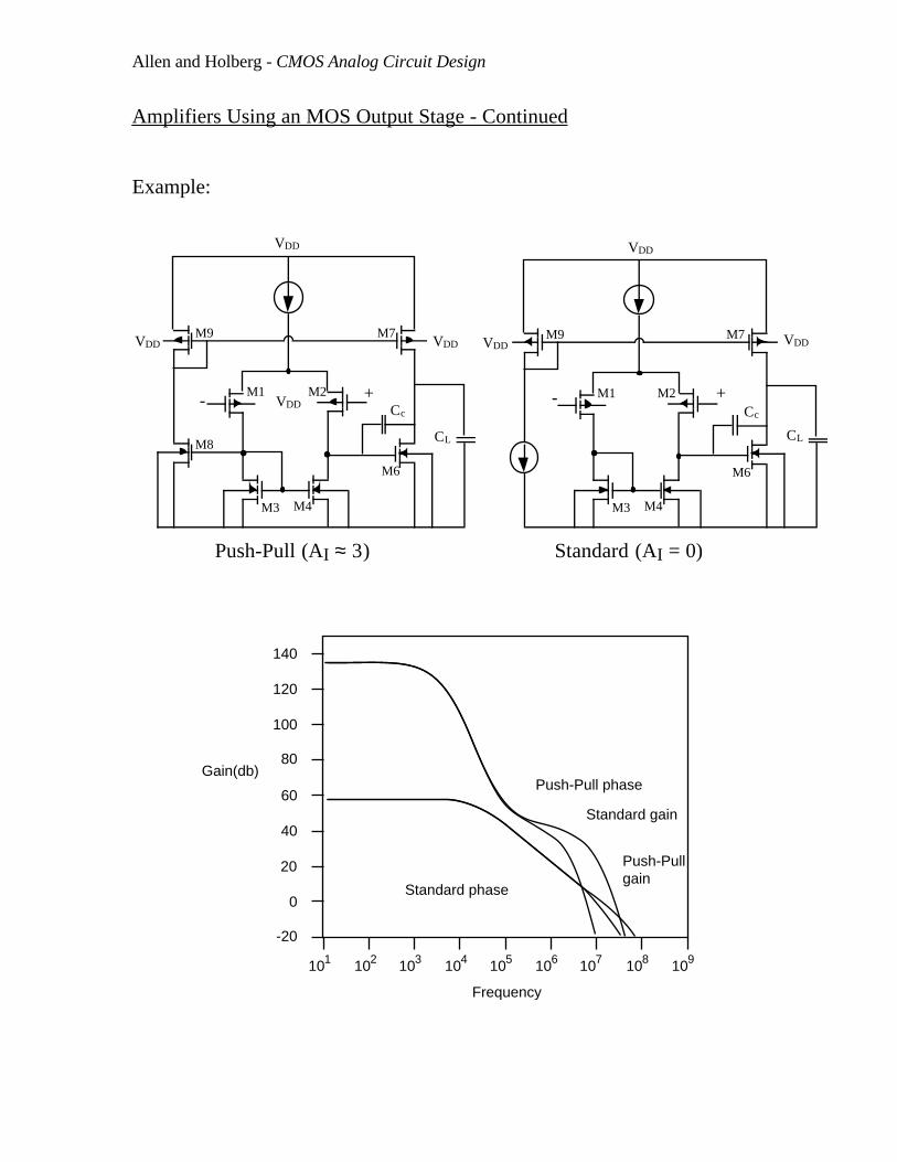
Allen and Holberg - CMOS Analog Circuit Design
Amplifiers Using an MOS Output Stage - Continued
Example:
M1 M2
M9 M7
M3 M4
M6
M1 M2
M9 M7
M8
M3 M4
M6
VDD
VDD
VDD VDD VDD VDD
CL CL
Cc Cc- + - +
VDD
Push-Pull (AI ≈ 3) Standard (AI = 0)
101 102 103 104 105 106 107 108 109
-20
40
60
80
100
120
140
0
20
Frequency
Gain(db)
Push-Pull gain
Standard gain
Push-Pull phase
Standard phase

Allen and Holberg - CMOS Analog Circuit Design
IX.2 Two-Stage Cascode Architecture
Why Cascode Op Amps?
• Control the frequency behavior
• Increase PSRR
• Simplifies design
Where is the Cascode Technique Applied?
• First stage -
Good noise performance
Requires level translation to second stage
Requires Miller compensation
• Second stage -
Self compensating
Reduces the efficiency of the Miller compensation
Increases PSRR
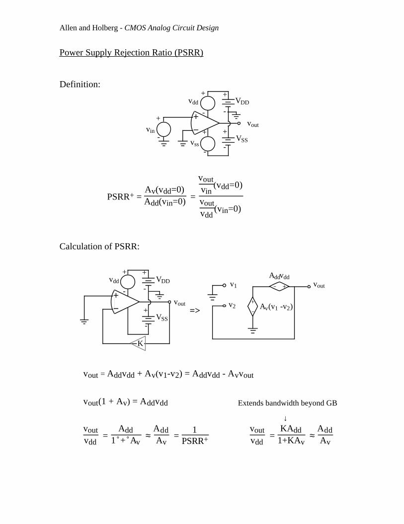
Allen and Holberg - CMOS Analog Circuit Design
Power Supply Rejection Ratio (PSRR)
Definition:
+
-
+
-
+
-
+
-
+
-vdd
vss
vinvout
VDD
VSS
PSRR+ = Av(vdd=0)Add(vin=0) =
voutvin
(vdd=0)
voutvdd
(vin=0)
Calculation of PSRR:
v1
v2 Av(v1 -v2)
Addvddvout
=>
+
-
+
-
+
-vdd
vout
VDD
VSS
K
vout = Addvdd + Av(v1-v2) = Addvdd - Avvout
vout(1 + Av) = Addvdd Extends bandwidth beyond GB
↓voutvdd
= Add
1 + Av ≈
AddAv
= 1
PSRR+ voutvdd
= KAdd
1+KAv ≈
AddAv
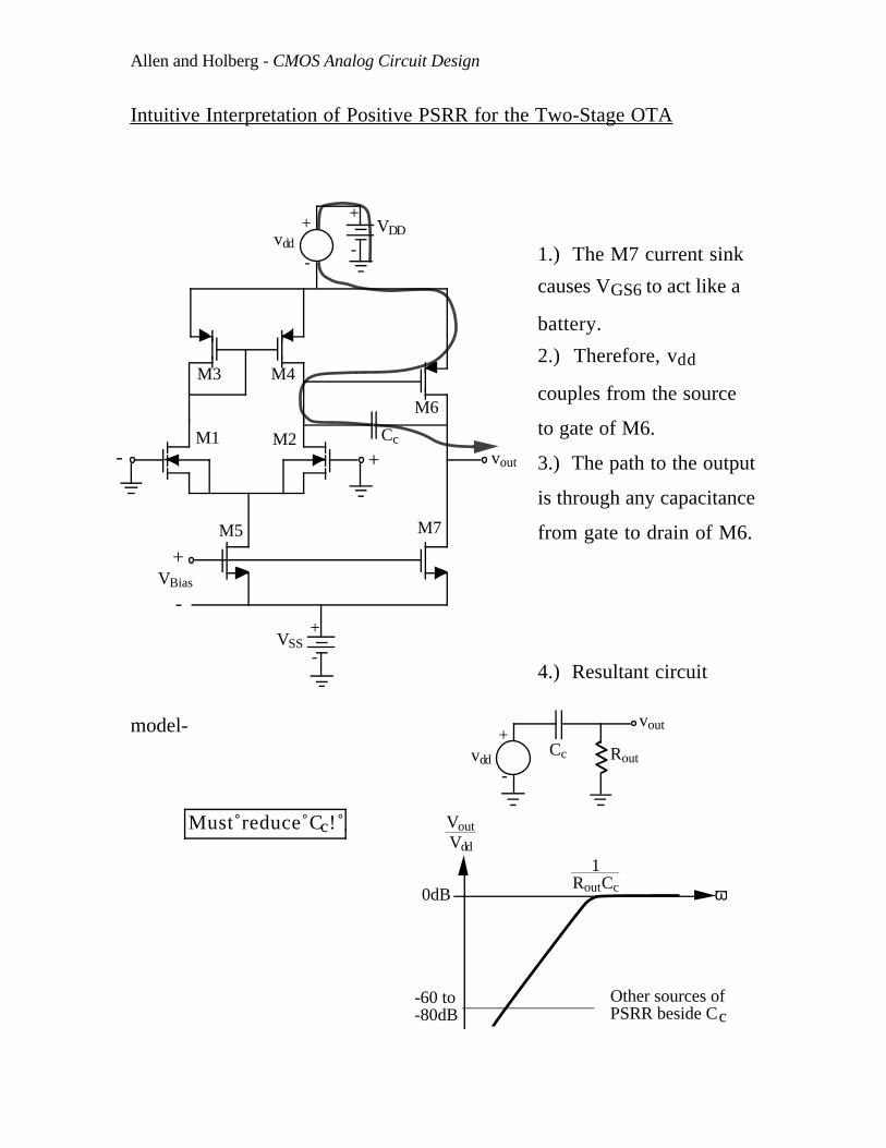
Allen and Holberg - CMOS Analog Circuit Design
Intuitive Interpretation of Positive PSRR for the Two-Stage OTA
1.) The M7 current sink
causes VGS6 to act like a
battery.
2.) Therefore, vdd
couples from the source
to gate of M6.
3.) The path to the output
is through any capacitance
from gate to drain of M6.
4.) Resultant circuit
model-
Must reduce Cc!
M4M3
M1+-
M2
M5
M6
M7
+
-VBias
+
-
+
-
+
-vdd
vout
VDD
VSS
Cc
vdd
+
-
vout
Cc Rout
VoutVdd
1RoutCc ω0dB
Other sources ofPSRR beside Cc
-60 to-80dB
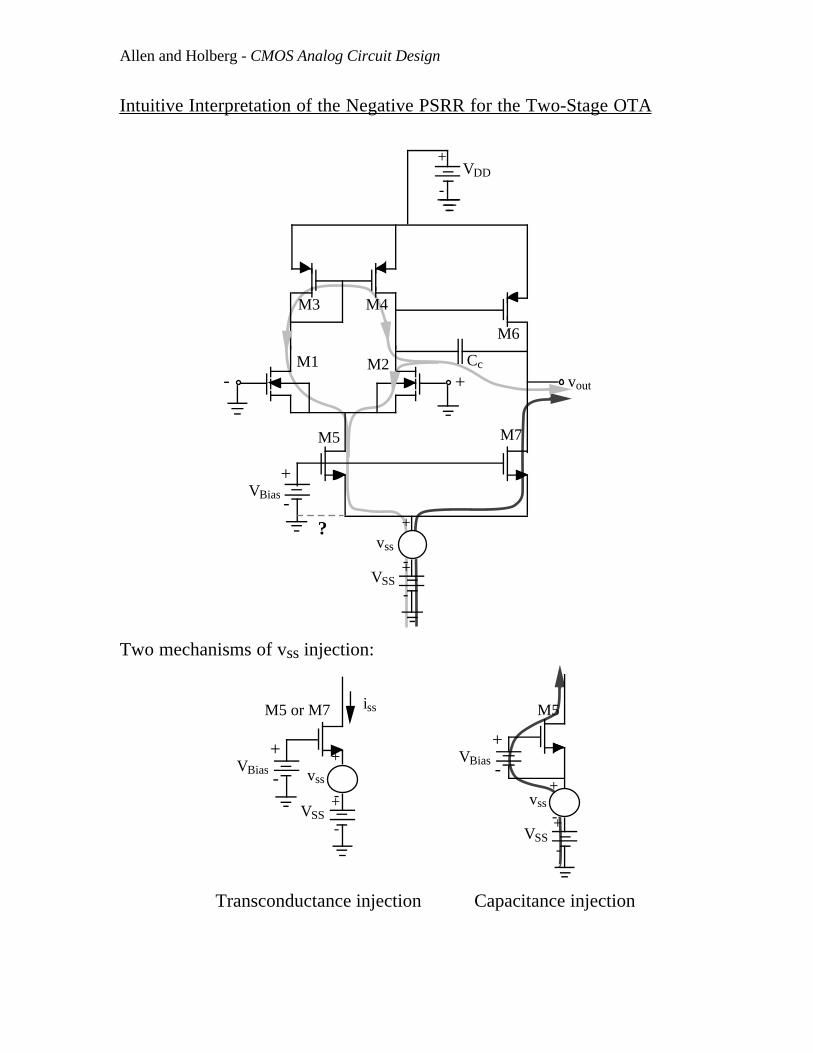
Allen and Holberg - CMOS Analog Circuit Design
Intuitive Interpretation of the Negative PSRR for the Two-Stage OTA
M4M3
M1+-
M2
M5
M6
M7
VBias
+
-+
-
+
-
vss
vout
VDD
VSS
Cc
+
-?
Two mechanisms of vss injection:
M5 or M7
VBias+
-+
-
vss
VSS
+
-
iss M5
VBias
+
-+
-
vss
VSS
+
-
Transconductance injection Capacitance injection
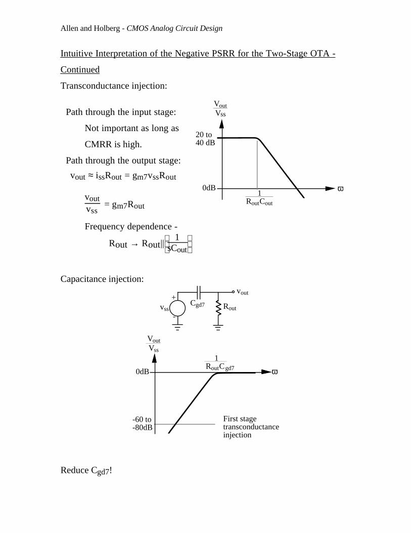
Allen and Holberg - CMOS Analog Circuit Design
Intuitive Interpretation of the Negative PSRR for the Two-Stage OTA -
Continued
Transconductance injection:
Path through the input stage:
Not important as long as
CMRR is high.
Path through the output stage:
vout ≈ issRout = gm7vssRout
voutvss
= gm7Rout
Frequency dependence -
Rout → Rout||
1
sCout
Capacitance injection:
+
-
vout
RoutvssCgd7
ω0dB
First stage transconductance injection
-60 to-80dB
VoutVss
1RoutCgd7
Reduce Cgd7!
VoutV
ω0dB
20 to 40 dB
1RoutCout
ss

Allen and Holberg - CMOS Analog Circuit Design
Problems with the two-stage OTA:
• Insufficient gain
• Poor stability for large load capacitance
• Poor PSRR
These problems can be addressed using various cascode structures.
We will consider several approaches:
• Cascoding the first stage
• Cascoding the second stage
• Folded cascode
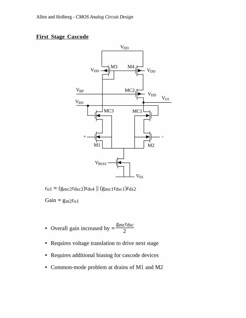
Allen and Holberg - CMOS Analog Circuit Design
First Stage Cascode
VDD
VDDVDD
VDD
M3 M4
MC2
M1
MC3
+ -
M2
MC1
VSS
VBIAS
VBN
VBP
VO1
ro1 ≈ (gmc2rdsc2)rds4 || (gmc1rdsc1)rds2
Gain ≈ gm2ro1
• Overall gain increased by ≈ gmcrdsc
2
• Requires voltage translation to drive next stage
• Requires additional biasing for cascode devices
• Common-mode problem at drains of M1 and M2
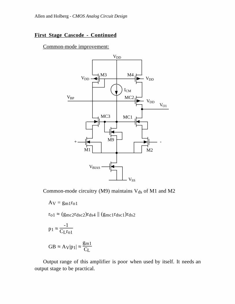
Allen and Holberg - CMOS Analog Circuit Design
First Stage Cascode - Continued
Common-mode improvement:
VDD
VDDM3
M1
MC3
+
VSS
VBIAS
VBP
VDD
VDD
M4
MC2
-
M2
MC1
VO1
ICM
M9
Common-mode circuitry (M9) maintains Vds of M1 and M2
AV = gm1ro1
ro1 ≈ (gmc2rdsc2)rds4 || (gmc1rdsc1)rds2
p1 ≈ -1
CLro1
GB ≈ AV|p1| ≈ gm1CL
Output range of this amplifier is poor when used by itself. It needs anoutput stage to be practical.
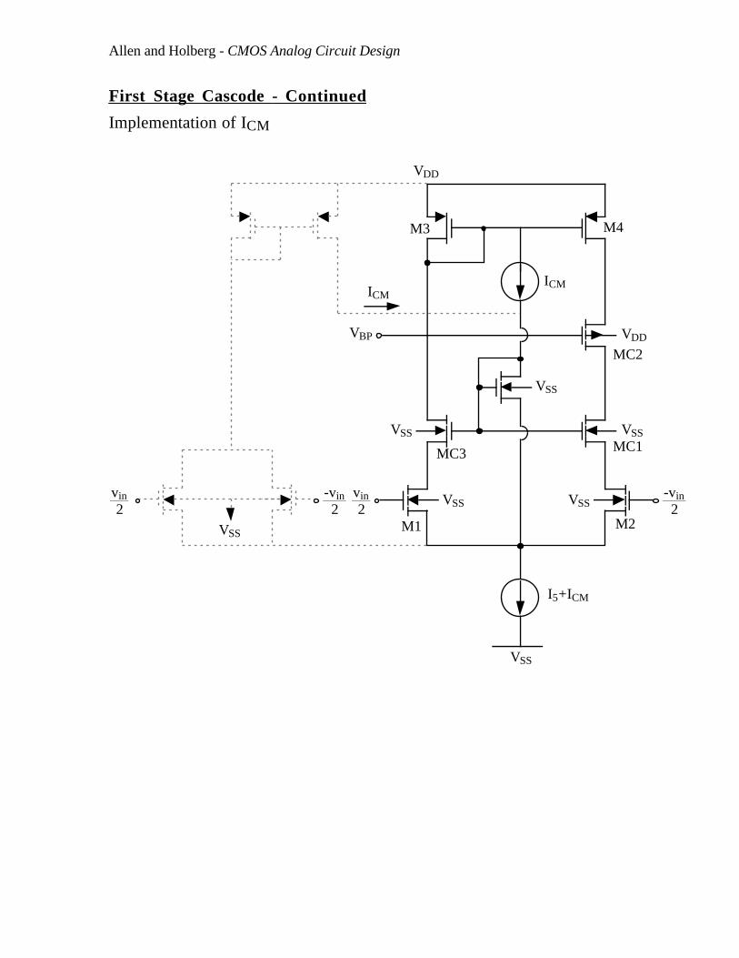
Allen and Holberg - CMOS Analog Circuit Design
First Stage Cascode - Continued
Implementation of ICM
VDD
VSS
VSS
VSS
VSSVSS
VSS
ICM
VBP
VDD
VSS
I5+ICM
vin2
-vin2
vin2
-vin2
ICM
M3 M4
MC2
MC1MC3
M1 M2
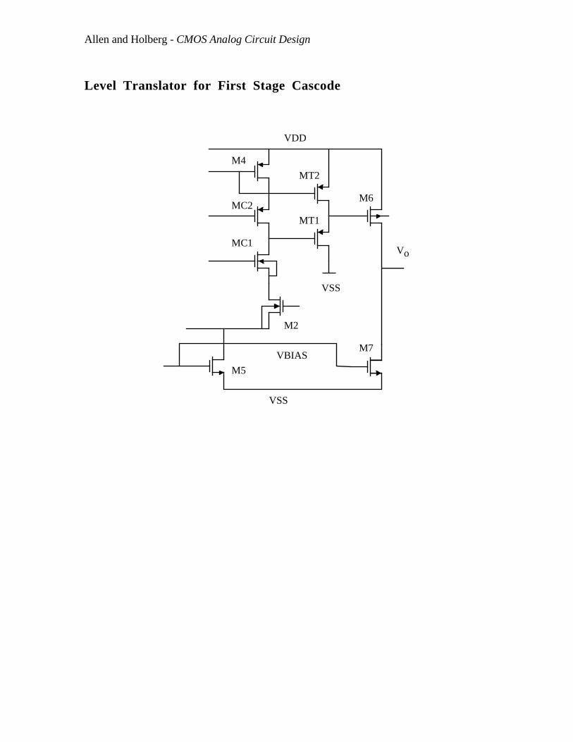
Allen and Holberg - CMOS Analog Circuit Design
Level Translator for First Stage Cascode
M4
M6
MT1
MT2
MC1
MC2
M7
M5
M2
VSS
VSS
VDD
Vo
VBIAS
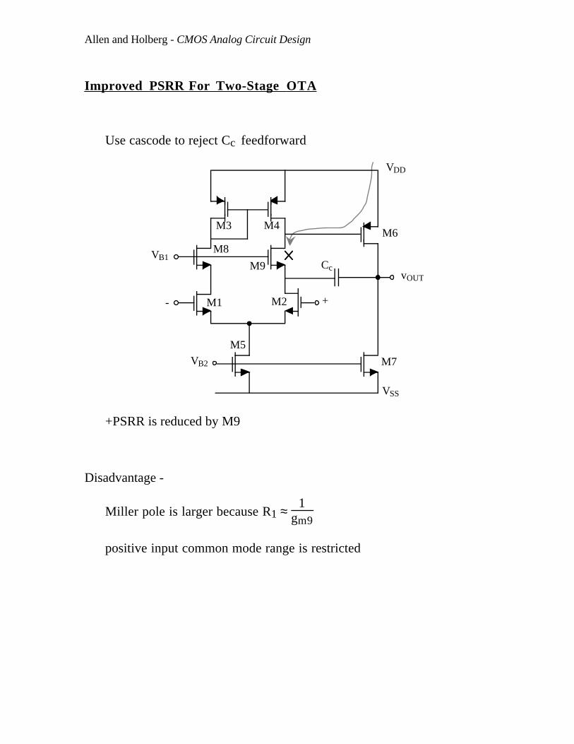
Allen and Holberg - CMOS Analog Circuit Design
Improved PSRR For Two-Stage OTA
Use cascode to reject Cc feedforward
M4M3M6
VDD
Cc
M5
M7
VSS
M1 M2- +
vOUTM9
M8VB1
VB2
+PSRR is reduced by M9
Disadvantage -
Miller pole is larger because R1 ≈ 1
gm9
positive input common mode range is restricted
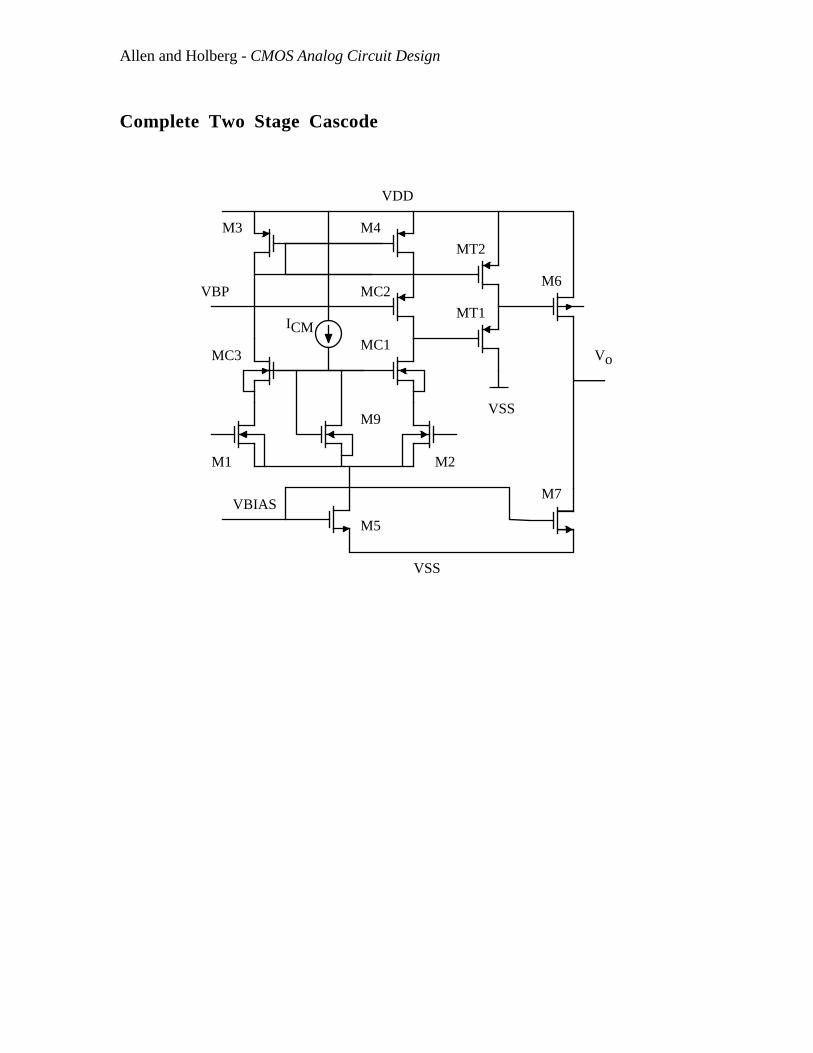
Allen and Holberg - CMOS Analog Circuit Design
Complete Two Stage Cascode
M4
M6
MT1
MT2
MC1
MC2
M7
M5
M2
VSS
VSS
VDD
Vo
VBIAS
M3
MC3
M1
M9
ICM
VBP
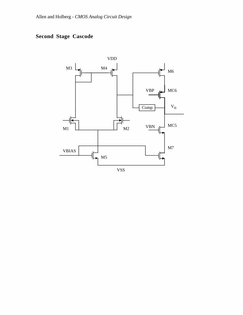
Allen and Holberg - CMOS Analog Circuit Design
Second Stage Cascode
M4M6
M7
M5
M2
VSS
VDD
Vo
VBIAS
M3
M1
MC6
MC5
Comp
VBP
VBN
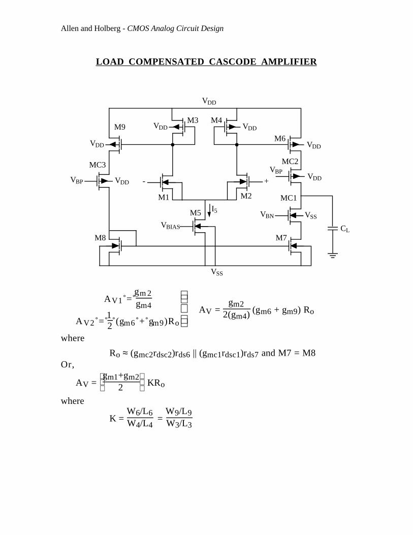
Allen and Holberg - CMOS Analog Circuit Design
LOAD COMPENSATED CASCODE AMPLIFIER
VDD VDD
VDD
VDD VDD
VDD
VSS
M6
M7
VSS
VDD
M1
+-
MC3
M3 M4
MC2
MC1
CL
M2
VBP
VBP
VBN
VBIAS
M9
M8
M5 I5
AV1 =
gm 2gm4
AV2 = 12 (gm6 + gm9)Ro
AV = gm2
2(gm4) (gm6 + gm9) Ro
where
Ro ≈ (gmc2rdsc2)rds6 || (gmc1rdsc1)rds7 and M7 = M8Or,
AV =
gm1+gm2
2 KRo
where
K = W6/L6W4/L4
= W9/L9W3/L3
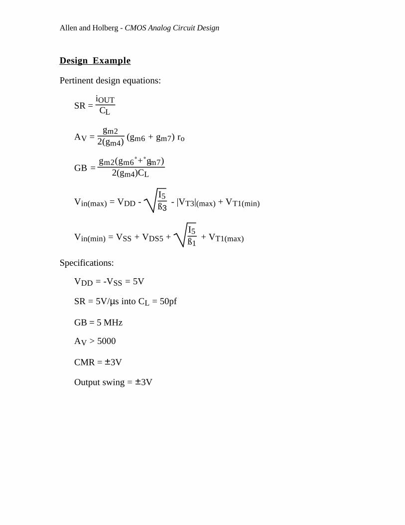
Allen and Holberg - CMOS Analog Circuit Design
Design Example
Pertinent design equations:
SR = iOUTCL
AV = gm2
2(gm4) (gm6 + gm7) ro
GB = gm2(gm6 + gm7)
2(gm4)CL
Vin(max) = VDD - I5ß3
- |VT3|(max) + VT1(min)
Vin(min) = VSS + VDS5 + I5ß1
+ VT1(max)
Specifications:
VDD = -VSS = 5V
SR = 5V/µs into CL = 50pf
GB = 5 MHz
AV > 5000
CMR = ±3V
Output swing = ±3V
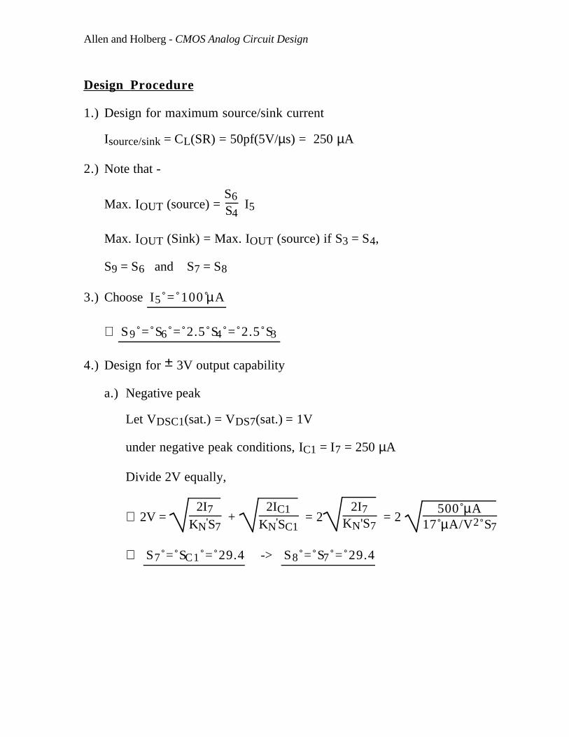
Allen and Holberg - CMOS Analog Circuit Design
Design Procedure
1.) Design for maximum source/sink current
Isource/sink = CL(SR) = 50pf(5V/µs) = 250 µA
2.) Note that -
Max. IOUT (source) = S6S4
I5
Max. IOUT (Sink) = Max. IOUT (source) if S3 = S4,
S9 = S6 and S7 = S8
3.) Choose I5 = 100 µA
∴ S9 = S6 = 2.5 S4 = 2.5 S3
4.) Design for ± 3V output capability
a.) Negative peak
Let VDSC1(sat.) = VDS7(sat.) = 1V
under negative peak conditions, IC1 = I7 = 250 µA
Divide 2V equally,
∴ 2V = 2I7
KN'S7 +
2IC1
KN'SC1 = 2
2I7KN'S7
= 2 500 µA
17 µA/V2 S7
∴ S7 = SC1 = 29.4 -> S8 = S7 = 29.4
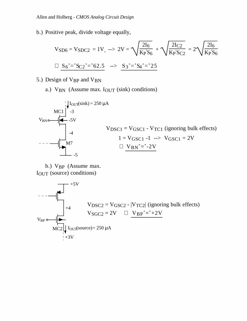
Allen and Holberg - CMOS Analog Circuit Design
b.) Positive peak, divide voltage equally,
VSD6 = VSDC2 = 1V, --> 2V = 2I6
KP'S6 +
2IC2
KP'SC2 = 2
2I6
KP'S6
∴ S6 = SC2 = 62.5 --> S3 = S4 = 25
5.) Design of VBP and VBN
a.) VBN (Assume max. IOUT (sink) conditions)
-5V
-5
-4
-3
IOUT(sink)
MC1
M7
VBN
= 250 µA
b.) VBP (Assume max.IOUT (source) conditions)
+3V
MC2
VBP
+5V
+4
IOUT(source)= 250 µA
VDSC1 = VGSC1 - VTC1 (ignoring bulk effects)
1 = VGSC1 -1 --> VGSC1 = 2V
∴ VBN = -2V
VDSC2 = VGSC2 - |VTC2| (ignoring bulk effects)
VSGC2 = 2V ∴ VBP = +2V
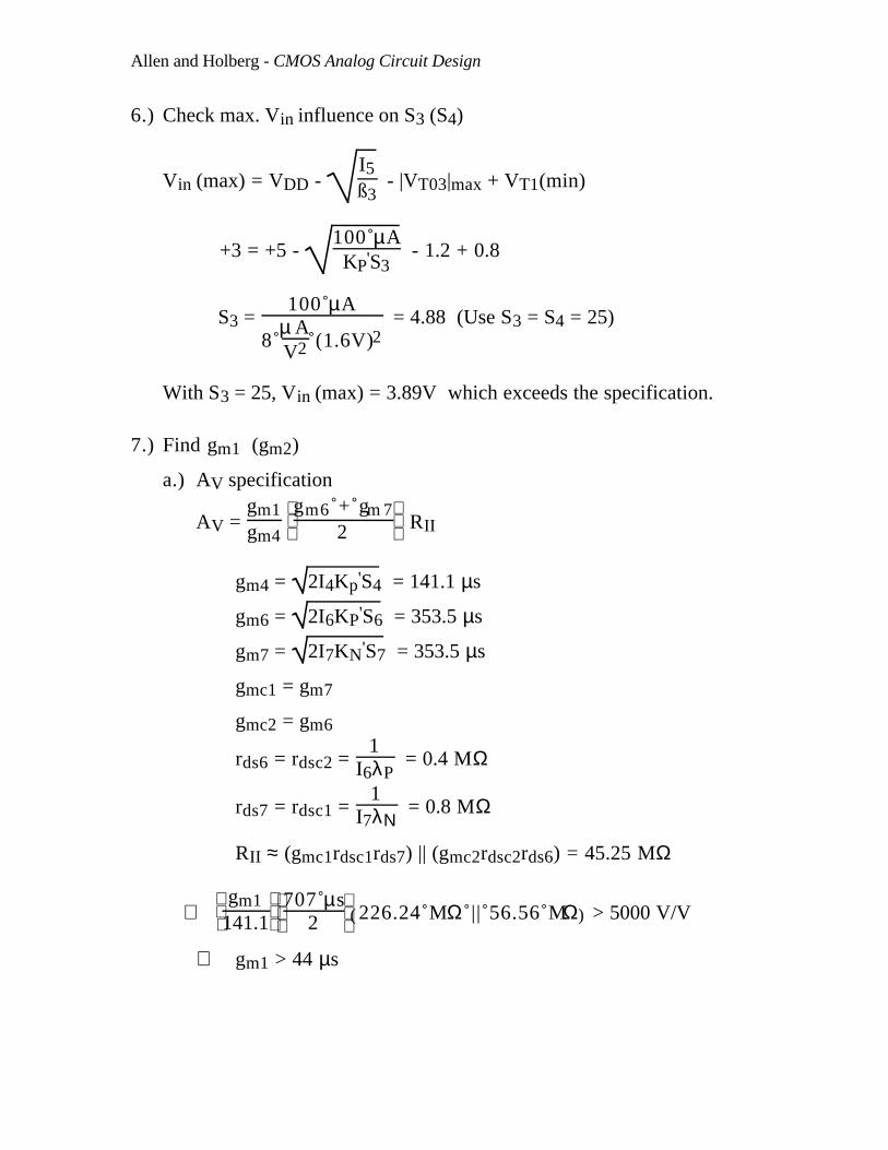
Allen and Holberg - CMOS Analog Circuit Design
6.) Check max. Vin influence on S3 (S4)
Vin (max) = VDD - I5ß3
- |VT03|max + VT1(min)
+3 = +5 - 100 µA
KP'S3 - 1.2 + 0.8
S3 = 100 µA
8 µ AV2 (1.6V)2
= 4.88 (Use S3 = S4 = 25)
With S3 = 25, Vin (max) = 3.89V which exceeds the specification.
7.) Find gm1 (gm2)
a.) AV specification
AV = gm1gm4
gm6 + gm 7
2 RII
gm4 = 2I4Kp'S4 = 141.1 µs
gm6 = 2I6KP'S6 = 353.5 µs
gm7 = 2I7KN'S7 = 353.5 µs
gmc1 = gm7
gmc2 = gm6
rds6 = rdsc2 = 1
I6λP = 0.4 MΩ
rds7 = rdsc1 = 1
I7λΝ = 0.8 MΩ
RII ≈ (gmc1rdsc1rds7) || (gmc2rdsc2rds6) = 45.25 MΩ
∴
gm1
141.1
707 µs
2 ( )226.24 MΩ || 56.56 MΩ > 5000 V/V
∴ gm1 > 44 µs
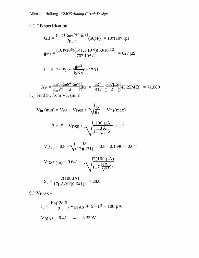
Allen and Holberg - CMOS Analog Circuit Design
b.) GB specification
GB = gm1(gm6 + gm7)
2gm4(50pF) = 10π.106 rps
gm1 = (10π.106)(141.1.10-6)(50.10-12)
707.10-6/2 = 627 µS
∴ S1 = S2 = gm2
I5KN' = 231
AV = gm1gm4
gm6+gm7
2 RII = 627
141.1
707µS
2 (45.25MΩ) = 71,080
8.) Find S5 from Vin (min)
Vin (min) = VSS + VDS5 + I5ß1
+ VT1(max)
-3 = -5 + VDS5 + 100 µA
17 µ AV2 S1
+ 1.2
VDS5 = 0.8 - 100
(17)(231) = 0.8 - 0.1596 = 0.641
VDS5 (sat) = 0.641 = 2(100 µA)
(17 µ AV2)S5
S5 = 2(100µA)
17µA/V2(0.641)2 = 28.6
9.) VBIAS -
I5 = KN'.28.6
2 ( )VBIAS + 5 -1 2 = 100 µA
VBIAS = 0.411 - 4 = -3.359V

Allen and Holberg - CMOS Analog Circuit Design
10.) Summary of design -
S1 = S2 = 231 S7 = S8 = SC1 = 29.4S3 = S4 = 25 VBP = 2VS5 = 28.6 VBN = -2VS6 = S9 = SC2 = SC3 = 62.5 VBIAS = -3.359V
11.) Check on power dissipation
Pdiss = 10(I8 + I5 + I7) = 10(125µA + 100µA + 125µA)
= 3.5mW
12.) Design W's for lateral diffusion and simulate
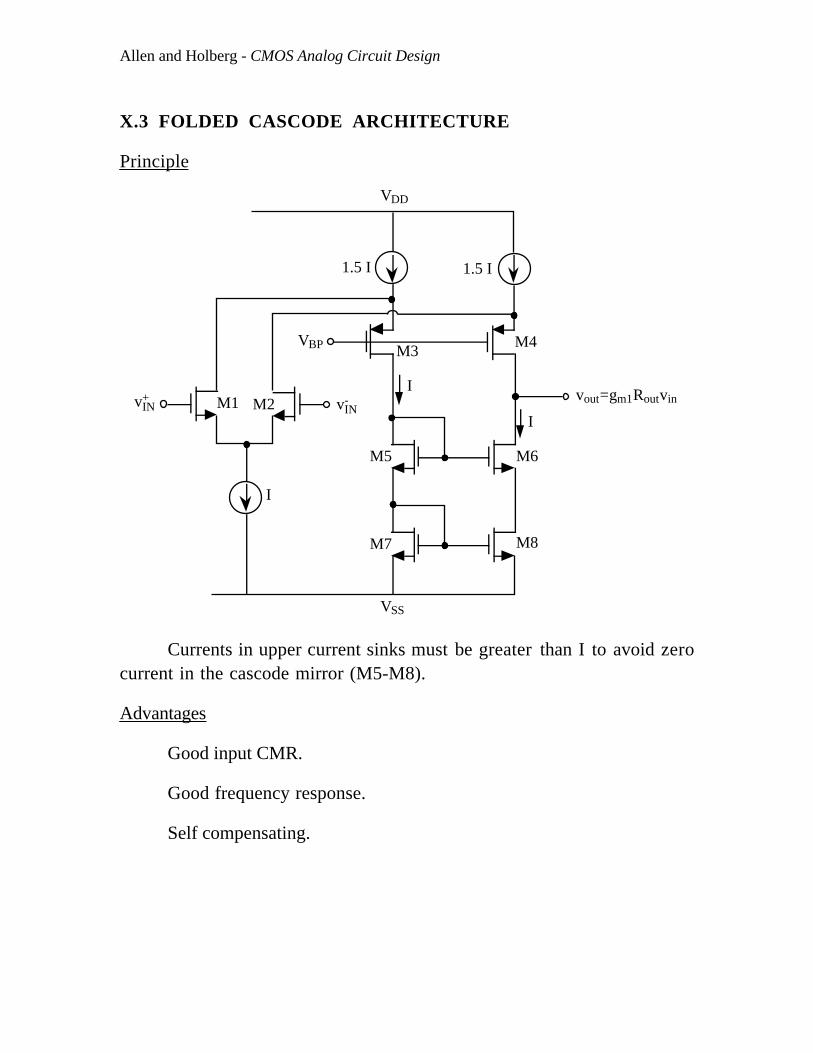
Allen and Holberg - CMOS Analog Circuit Design
X.3 FOLDED CASCODE ARCHITECTURE
Principle
1.5 I 1.5 I
I
I
M6
M8
M5
M7
M4M3
I
M1 M2
VDD
VSS
VBP
vout=gm1RoutvinvIN+ vIN
-
Currents in upper current sinks must be greater than I to avoid zerocurrent in the cascode mirror (M5-M8).
Advantages
Good input CMR.
Good frequency response.
Self compensating.

Allen and Holberg - CMOS Analog Circuit Design
Folded Cascode OP Amp
VSS
M14
M15
M16
M9
M11
M13M12
M10
M5
M8
M4M3
M1 M2
VDD
VB2
VB1
VB3
+-
Cc
VOUT
VB3
High gain, High speed, cascode amp
GB ≈ 10 MHz, AVDC ≈ 100 dB
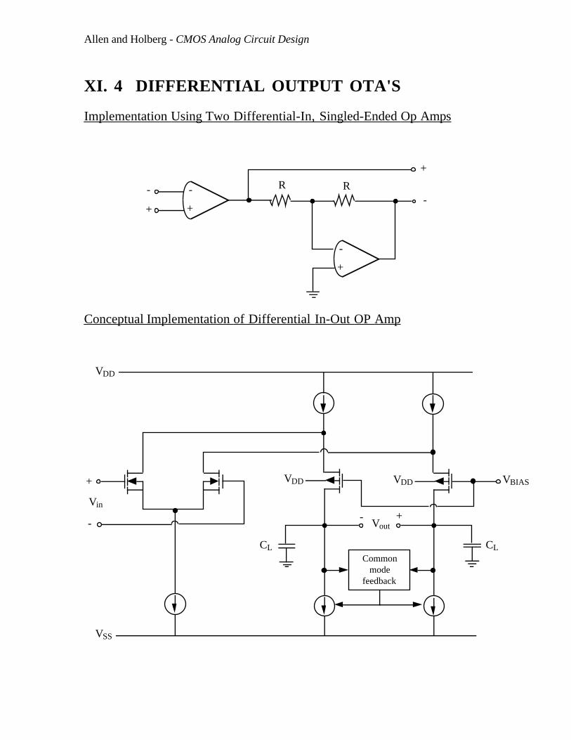
Allen and Holberg - CMOS Analog Circuit Design
XI. 4 DIFFERENTIAL OUTPUT OTA'S
Implementation Using Two Differential-In, Singled-Ended Op Amps
+
-
+
-
-
+
R R
+
-
Conceptual Implementation of Differential In-Out OP Amp
VDD VDD+
-
Common modefeedback
+-
VSS
VDD
Vin
CL CL
Vout
VBIAS
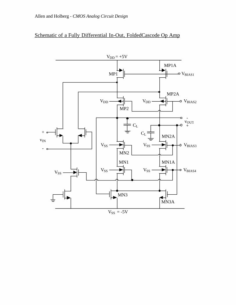
Allen and Holberg - CMOS Analog Circuit Design
Schematic of a Fully Differential In-Out, FoldedCascode Op Amp
VSS
VDD
VSS
VSS
VDD
VSS
VSS
VDD = +5V
VSS = -5V
MP1
MP1A
MP2A
MN2A
MN1A
MN3A
MN3
MN1
MN2
CL
CL
MP2
+
-
vIN
-
+vOUT
VBIAS1
VBIAS2
VBIAS3
VBIAS4
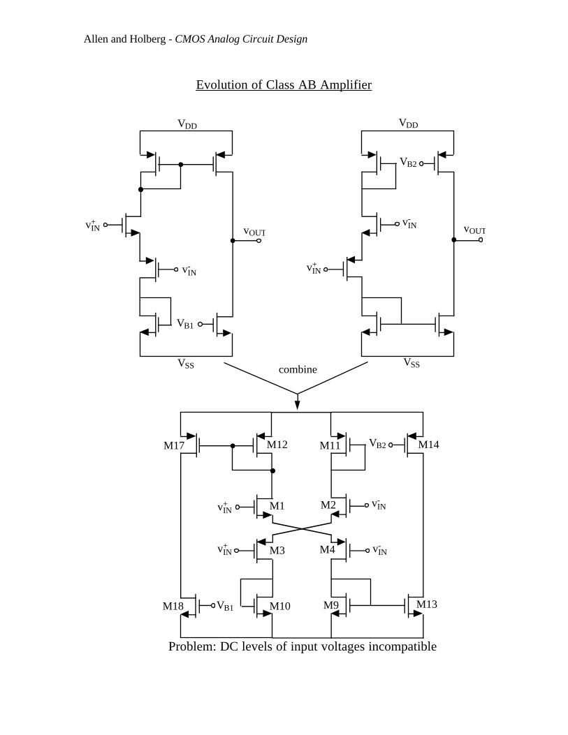
Allen and Holberg - CMOS Analog Circuit Design
Evolution of Class AB Amplifier
VB1
vIN+
vIN+
vIN-
vIN-
VB2M17
M18 M10 M9
M3
M2M1
M4
M13
M11 M14M12
combine
VDD
VSS
vOUT
VB1
vIN+
vIN-
VDD
VSS
vOUT
vIN+
vIN-
VB2
Problem: DC levels of input voltages incompatible
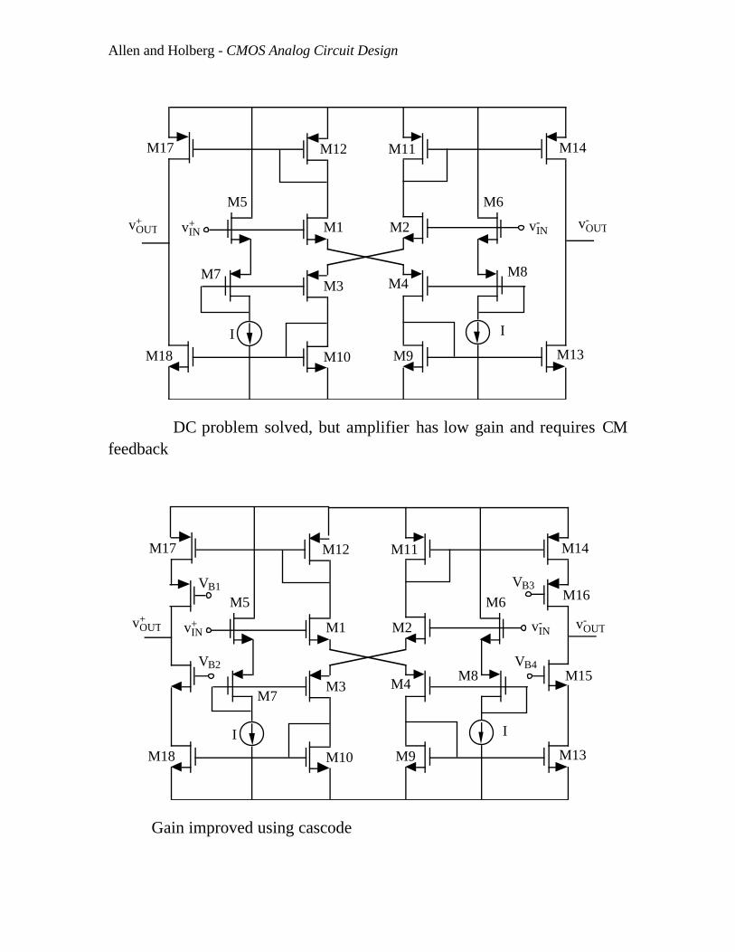
Allen and Holberg - CMOS Analog Circuit Design
vIN+
M17
M18 M10 M9
M3
M2M1
M4
M11
M13
M14M12
vIN-
M8
M6M5
M7
vOUT-vOUT
+
I I
DC problem solved, but amplifier has low gain and requires CMfeedback
vIN+
M17
M18 M10 M9
M3
M2M1
M4
M11
M13
M14M12
vIN-
M8
M6M5
M7
vOUT-vOUT
+
I I
M16
M15
VB3
VB4
VB1
VB2
Gain improved using cascode
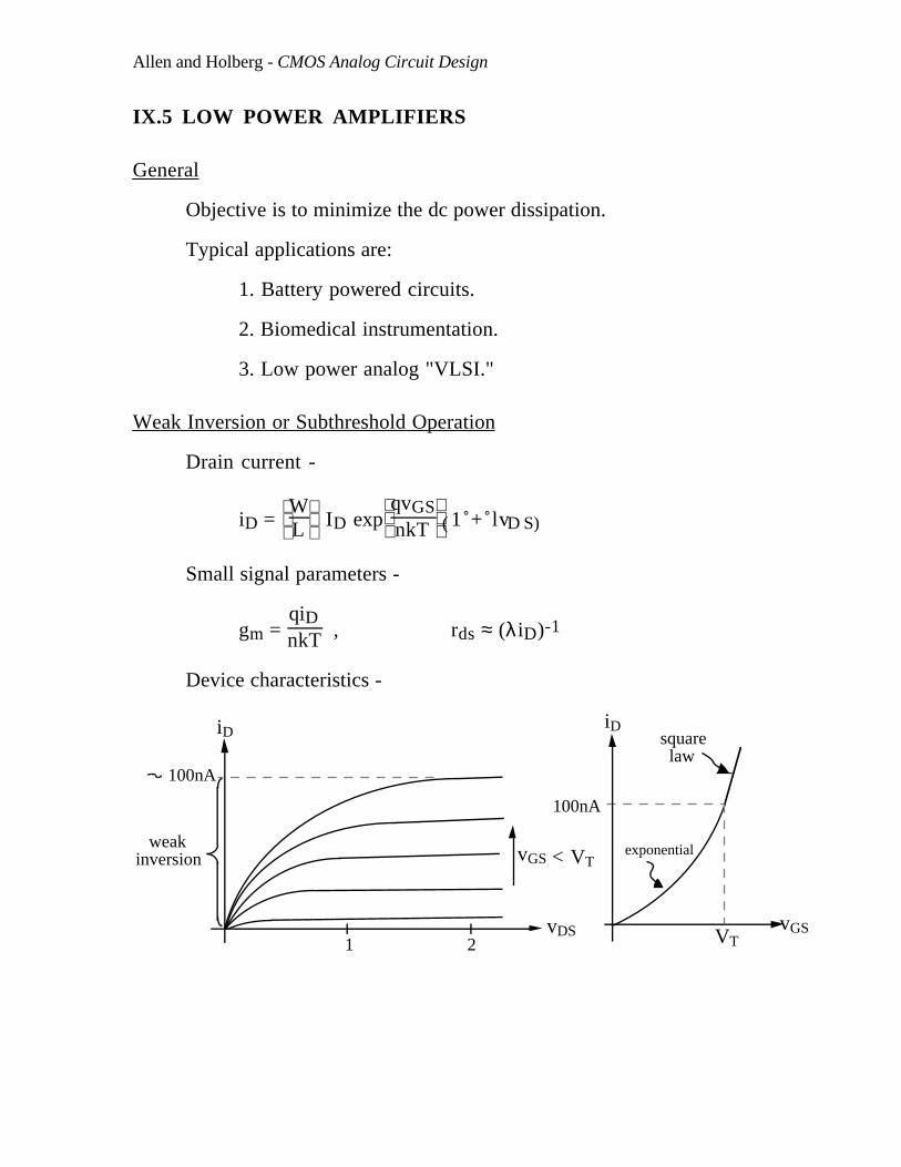
Allen and Holberg - CMOS Analog Circuit Design
IX.5 LOW POWER AMPLIFIERS
General
Objective is to minimize the dc power dissipation.
Typical applications are:
1. Battery powered circuits.
2. Biomedical instrumentation.
3. Low power analog "VLSI."
Weak Inversion or Subthreshold Operation
Drain current -
iD =
W
L ID exp
qvGS
nkT ( )1 + lvD S
Small signal parameters -
gm = qiDnkT , rds ≈ (λ iD)-1
Device characteristics -
iD
vGS
square law
exponential
VT
100nA
vGS < VT
1 2
iD
vDS
100nA
weakinversion
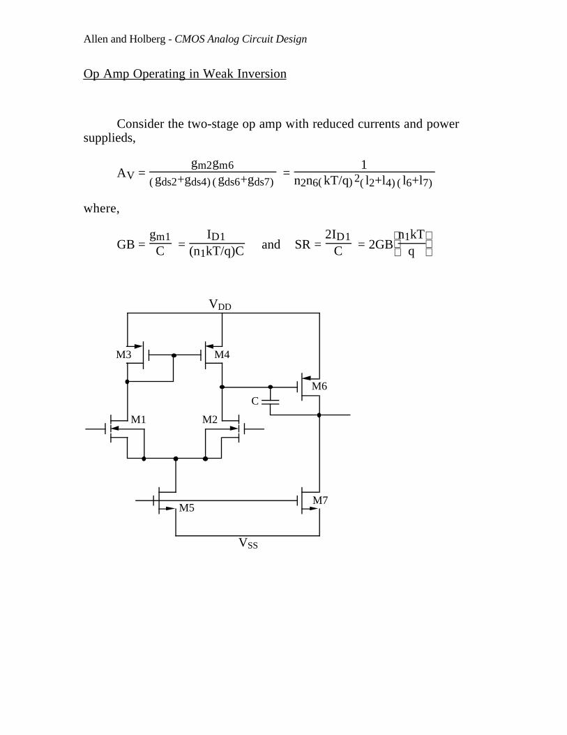
Allen and Holberg - CMOS Analog Circuit Design
Op Amp Operating in Weak Inversion
Consider the two-stage op amp with reduced currents and powersupplieds,
AV = gm2gm6
( )gds2+gds4 ( )gds6+gds7 =
1n2n6( )kT/q 2( )l2+l4 ( )l6+l7
where,
GB = gm1C =
ID1(n1kT/q)C and SR =
2ID1C = 2GB
n1kT
q
VDD
VSS
CM6
M4M3
M2M1
M5M7
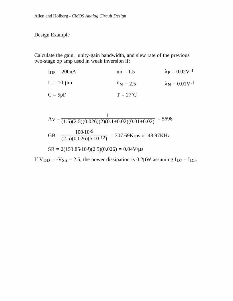
Allen and Holberg - CMOS Analog Circuit Design
Design Example
Calculate the gain, unity-gain bandwidth, and slew rate of the previoustwo-stage op amp used in weak inversion if:
ID5 = 200nA nP = 1.5 λP = 0.02V-1
L = 10 µm nN = 2.5 λN = 0.01V-1
C = 5pF T = 27˚C
AV = 1
(1.5)(2.5)(0.026)(2)(0.1+0.02)(0.01+0.02) = 5698
GB = 100.10-9
(2.5)(0.026)(5.10-12) = 307.69Krps or 48.97KHz
SR = 2(153.85.103)(2.5)(0.026) = 0.04V/µs
If VDD = -VSS = 2.5, the power dissipation is 0.2µW assuming ID7 = ID5.
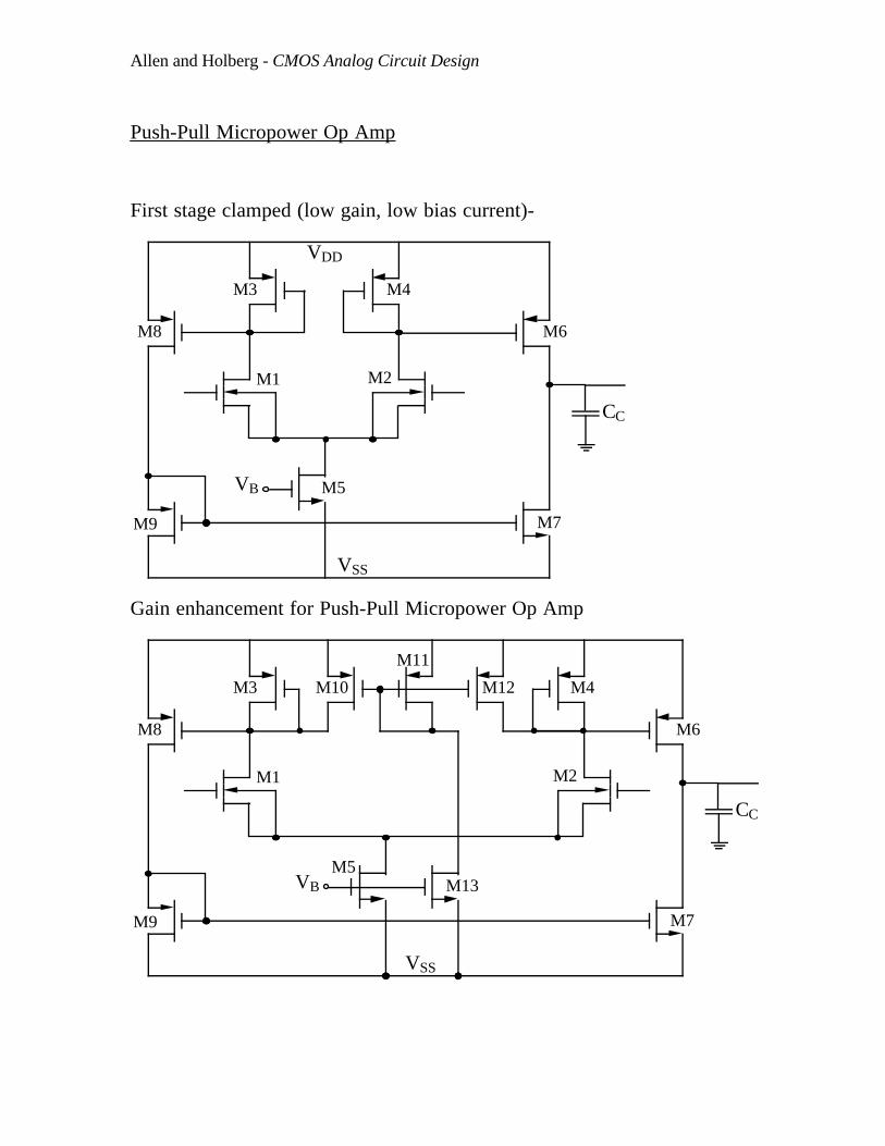
Allen and Holberg - CMOS Analog Circuit Design
Push-Pull Micropower Op Amp
First stage clamped (low gain, low bias current)-
VDD
VSS
M4M3
M2M1
M5
M6
M7
CC
VB
M9
M8
Gain enhancement for Push-Pull Micropower Op Amp
VSS
M3
M1
M5
M6
M7
CC
VB
M9
M8
M4
M2
M13
M11
M12M10
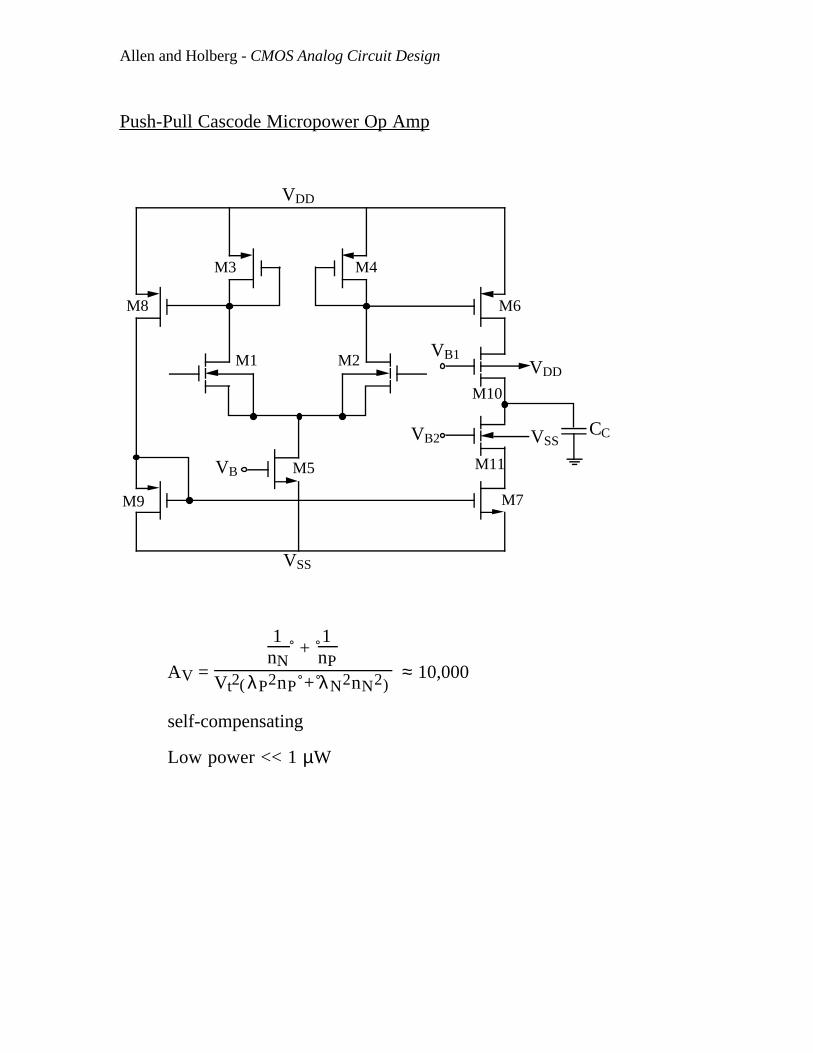
Allen and Holberg - CMOS Analog Circuit Design
Push-Pull Cascode Micropower Op Amp
VDD
VSS
M4M3
M2M1
M5
M6
M7
CC
VB
M9
M8
M11
VB1
VB2
M10
VDD
VSS
AV =
1nN
+ 1nP
Vt2( )λP2nP + λN2nN2 ≈ 10,000
self-compensating
Low power << 1 µW
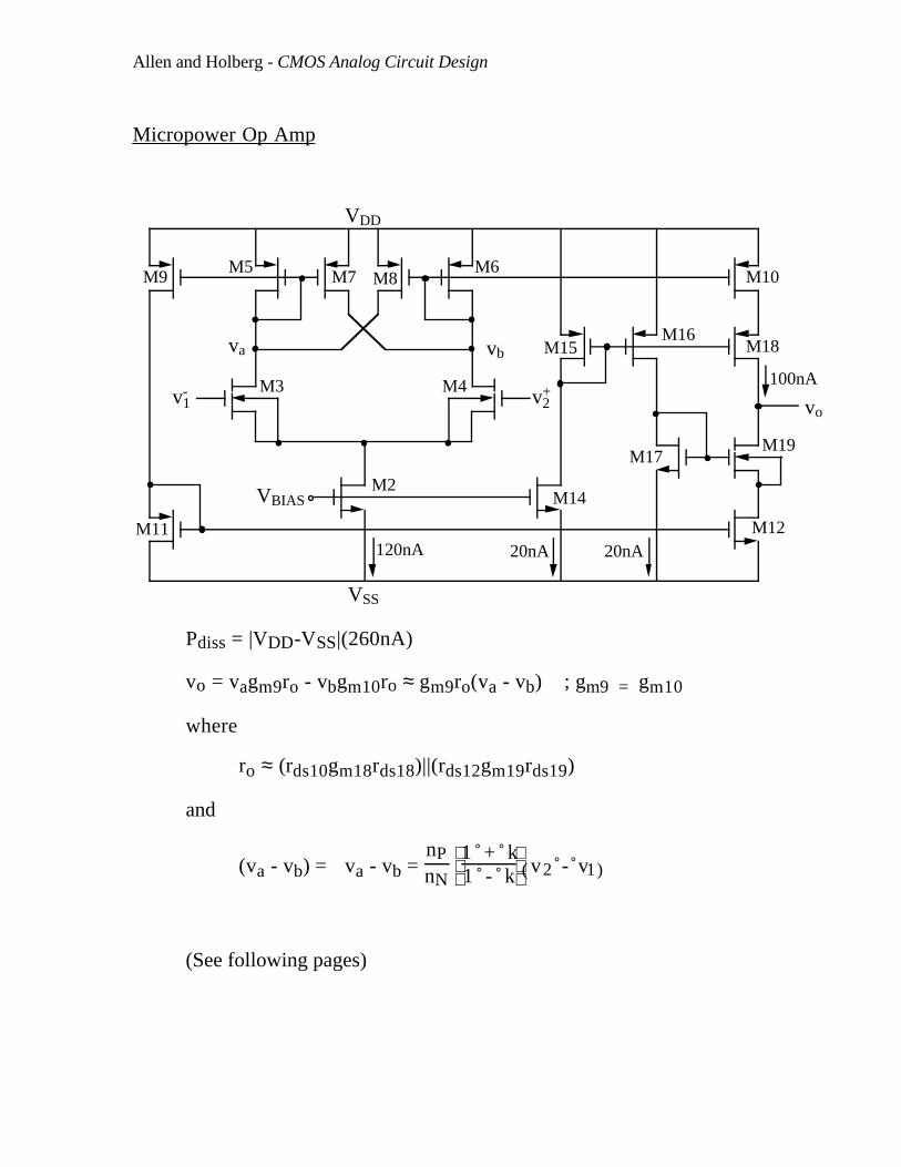
Allen and Holberg - CMOS Analog Circuit Design
Micropower Op Amp
VDD
M4M3
M2
M12
M5 M6M7
VSS
M9 M8
M11
M10
M14
M15M16
M18
M19M17
VBIAS
120nA 20nA
100nA
20nA
vbva
vov1
- v2+
Pdiss = |VDD-VSS|(260nA)
vo = vagm9ro - vbgm10ro ≈ gm9ro(va - vb) ; gm9 = gm10
where
ro ≈ (rds10gm18rds18)||(rds12gm19rds19)
and
(va - vb) = va - vb = nPnN
1 + k
1 - k ( )v2 - v1
(See following pages)
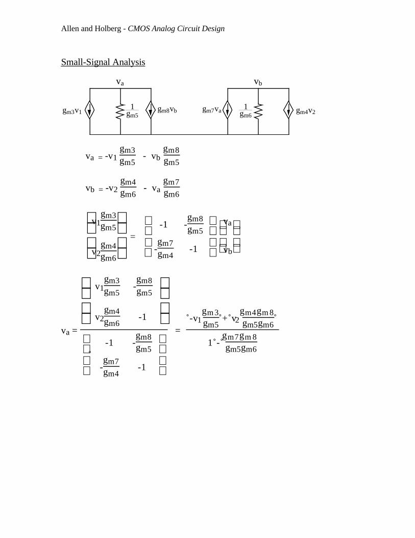
Allen and Holberg - CMOS Analog Circuit Design
Small-Signal Analysis
1gm5
gm8vbgm3v1
va
1gm6
gm7va gm4v2
vb
va = -v1 gm3gm5
- vb gm8gm5
vb = -v2 gm4gm6
- va gm7gm6
v1
gm3gm5
v2gm4gm6
=
-1 -
gm8gm5
-gm7gm4
-1
va
vb
va =
v1
gm3gm5
-gm8gm5
v2gm4gm6
-1
-1 -
gm8gm5
-gm7gm4
-1
= -v1
gm 3gm5
+ v2gm4gm 8gm5gm6
1 - gm7gm 8gm5gm6
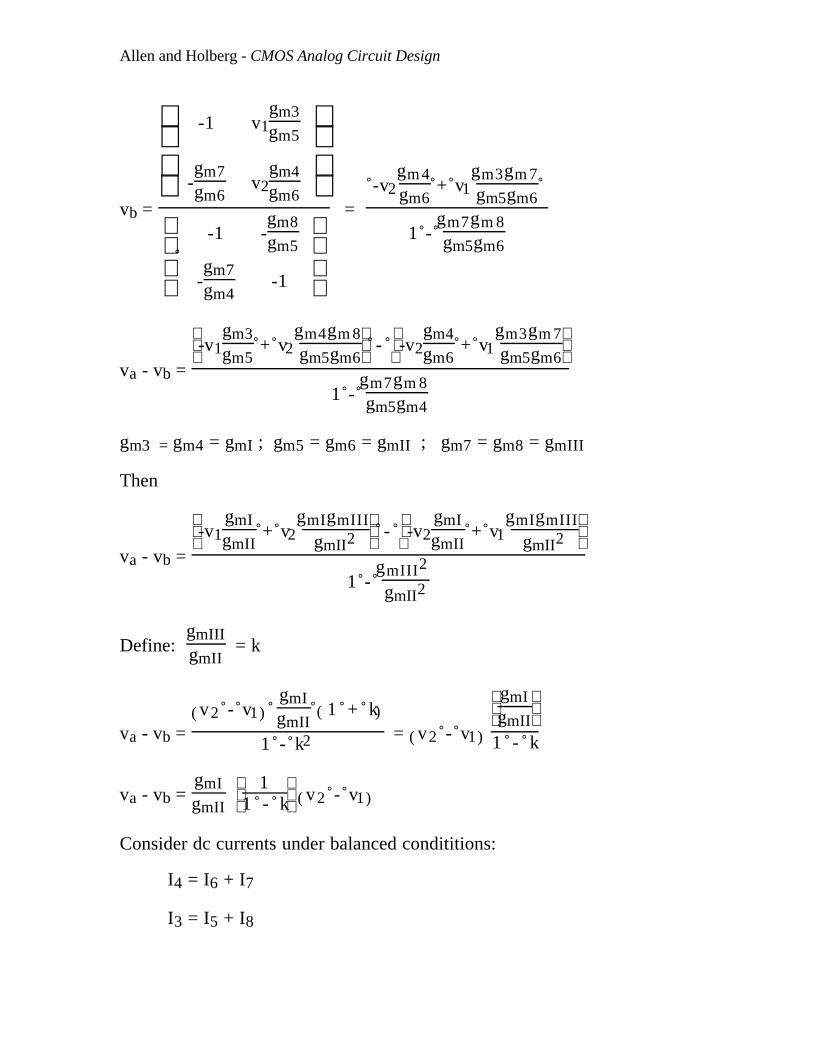
Allen and Holberg - CMOS Analog Circuit Design
vb =
-1 v1
gm3gm5
-gm7gm6
v2gm4gm6
-1 -
gm8gm5
-gm7gm4
-1
= -v2
gm 4gm6
+ v1gm3gm 7gm5gm6
1 - gm7gm 8gm5gm6
va - vb =
-v1gm3gm5
+ v2gm4gm 8gm5gm6
-
-v2gm4gm6
+ v1gm3gm 7gm5gm6
1 - gm7gm 8gm5gm4
gm3 = gm4 = gmI ; gm5 = gm6 = gmII ; gm7 = gm8 = gmIII
Then
va - vb =
-v1gmIgmII
+ v2gmIgmIII
gmII2 -
-v2gmIgmII
+ v1gmIgmIII
gmII2
1 - gmIII2
gmII2
Define: gmIIIgmII
= k
va - vb = ( )v2 - v1
gmIgmII
( )1 + k
1 - k2 = ( )v2 - v1
gmI
gmII
1 - k
va - vb = gmIgmII
1
1 - k ( )v2 - v1
Consider dc currents under balanced condititions:
I4 = I6 + I7
I3 = I5 + I8
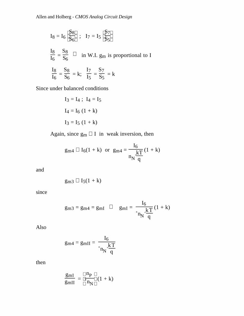
Allen and Holberg - CMOS Analog Circuit Design
I8 = I6
S8
S6 ; I7 = I5
S7
S5
I8I6
= S8S6
⇒ in W.I. gm is proportional to I
I8I6
= S8S6
= k; I7I5
= S7S5
= k
Since under balanced conditions
I3 = I4 ; I4 = I5
I4 = I6 (1 + k)
I3 = I5 (1 + k)
Again, since gm ∝ I in weak inversion, then
gm4 ∝ I6(1 + k) or gm4 = I6
nN kTq
(1 + k)
and
gm3 ∝ I5(1 + k)
since
gm3 = gm4 = gmI ⇒ gmI = I6
nN k Tq
(1 + k)
Also
gm4 = gmII = I6
nN k Tq
then
gmIgmII
=
nP
nN (1 + k)
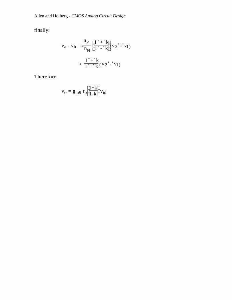
Allen and Holberg - CMOS Analog Circuit Design
finally:
va - vb = nP
nN
1 + k
1 - k ( )v2 - v1
≈ 1 + k1 - k ( )v2 - v1
Therefore,
vo = gm9 ro
1+k
1-k vid
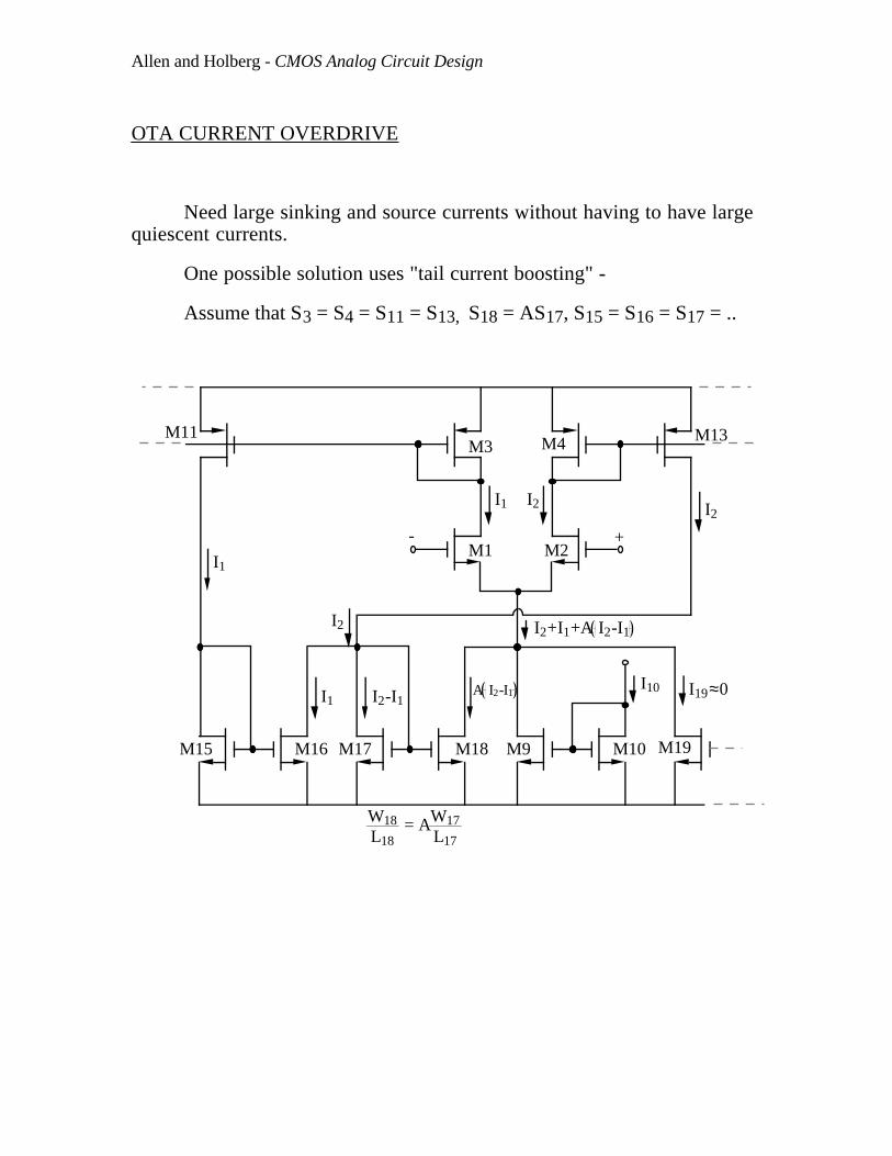
Allen and Holberg - CMOS Analog Circuit Design
OTA CURRENT OVERDRIVE
Need large sinking and source currents without having to have largequiescent currents.
One possible solution uses "tail current boosting" -
Assume that S3 = S4 = S11 = S13, S18 = AS17, S15 = S16 = S17 = ..
M11M3 M4
M1 M2
M13
+-
I1 I2 I2
I2
I1 I2-I1A I2-I1
I2+I1+A I2-I1
I10 I19≈0
M19M10M9M18M17M16M15
I1
W18L18
= AW17L17
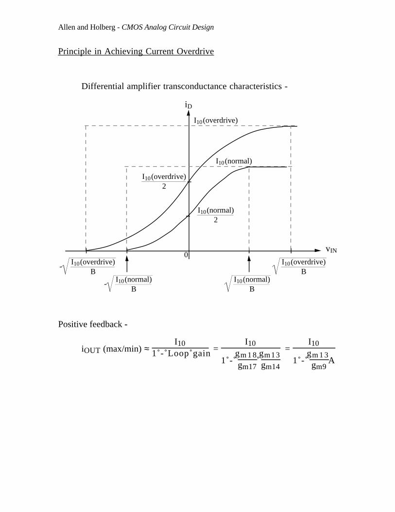
Allen and Holberg - CMOS Analog Circuit Design
Principle in Achieving Current Overdrive
Differential amplifier transconductance characteristics -
iD
I10(normal)
I10(normal)2
I10(overdrive)2
I10(overdrive)
0I10(overdrive)
B-
I10(overdrive)B
-I10(normal)
BI10(normal)
B
vIN
Positive feedback -
iOUT (max/min) ≈ I10
1 - Loop gain = I10
1 - gm 1 8gm17
gm13gm14
= I10
1 - gm 1 3
gm9A
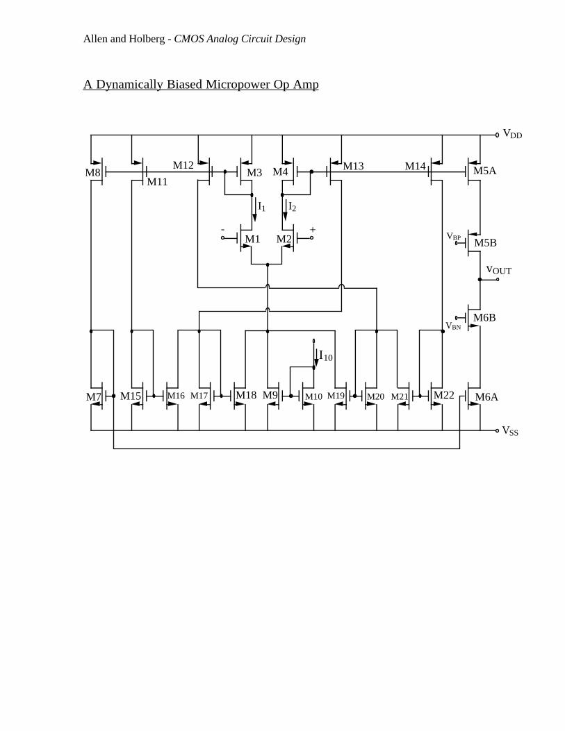
Allen and Holberg - CMOS Analog Circuit Design
A Dynamically Biased Micropower Op Amp
I1 I2
vOUT
M11M3 M4
M1 M2
M13
+-
M19M10M9M18M17M16M15 M21M20 M22
M12M8
M7
M5A
M5B
M6A
M6B
M14
I10
VBN
VBP
DDV
SSV
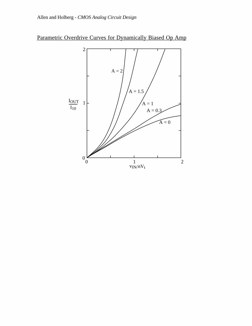
Allen and Holberg - CMOS Analog Circuit Design
Parametric Overdrive Curves for Dynamically Biased Op Amp
A = 0
A = 0.3A = 1
A = 1.5
A = 2
IOUT
I10
2
1
00 1 2
vIN/nVt
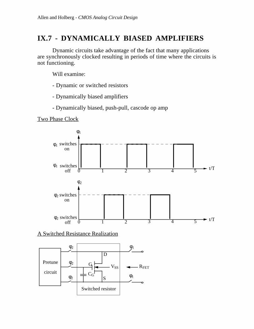
Allen and Holberg - CMOS Analog Circuit Design
IX.7 - DYNAMICALLY BIASED AMPLIFIERS
Dynamic circuits take advantage of the fact that many applicationsare synchronously clocked resulting in periods of time where the circuits isnot functioning.
Will examine:
- Dynamic or switched resistors
- Dynamically biased amplifiers
- Dynamically biased, push-pull, cascode op amp
Two Phase Clock
t/T0 1 2 3 4 5
φ1
switches on
φ1
switches off
φ1
t/T0 1 2 3 4 5
φ2
switches on
φ2
switches off
φ2
A Switched Resistance Realization
Pretune
circuit
φ2 φ1
φ2
φ1
VSS RFET
CG
G
D
S
Switched resistor
φ2
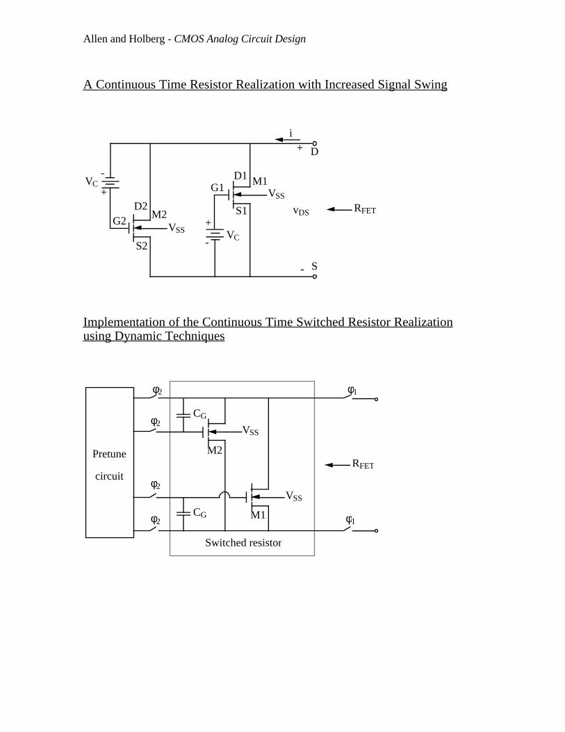
Allen and Holberg - CMOS Analog Circuit Design
A Continuous Time Resistor Realization with Increased Signal Swing
+
-VC
VSS
+
-VC
M2D2
G2
S2
VSS
M1G1
D1
S1
D
S
RFET
+
-
vDS
i
Implementation of the Continuous Time Switched Resistor Realization using Dynamic Techniques
Pretune
circuit
φ2 φ1
φ2
VSS
RFET
CG
Switched resistor
φ2
φ2 φ1
VSS
CG
M1
M2
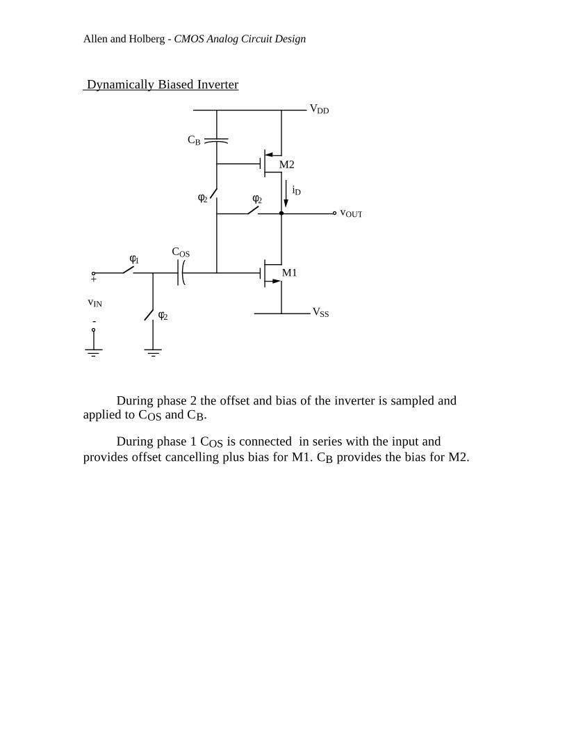
Allen and Holberg - CMOS Analog Circuit Design
Dynamically Biased Inverter
+
-
VDD
VSS
vOUT
M2
iD
CB
COS
vIN
M1φ1
φ2
φ2 φ2
During phase 2 the offset and bias of the inverter is sampled andapplied to COS and CB.
During phase 1 COS is connected in series with the input andprovides offset cancelling plus bias for M1. CB provides the bias for M2.
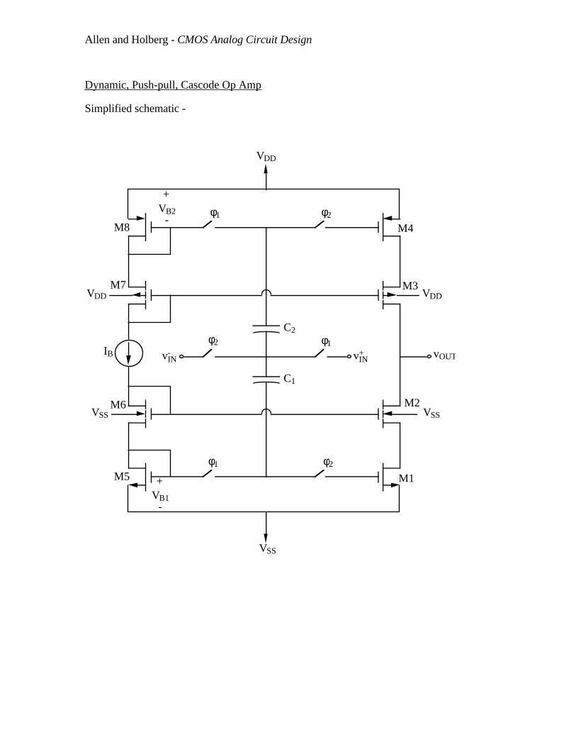
Allen and Holberg - CMOS Analog Circuit Design
Dynamic, Push-pull, Cascode Op Amp
Simplified schematic -
φ2 φ1
φ1
φ1 φ2
φ2
M8
M7
M6
M5 M1
M2
M3
M4
C1
C2
VSS
VSS
VSS
VDDVDD
VDD
+
-VB1
VB2
+
-
IB vOUTvIN- vIN
+
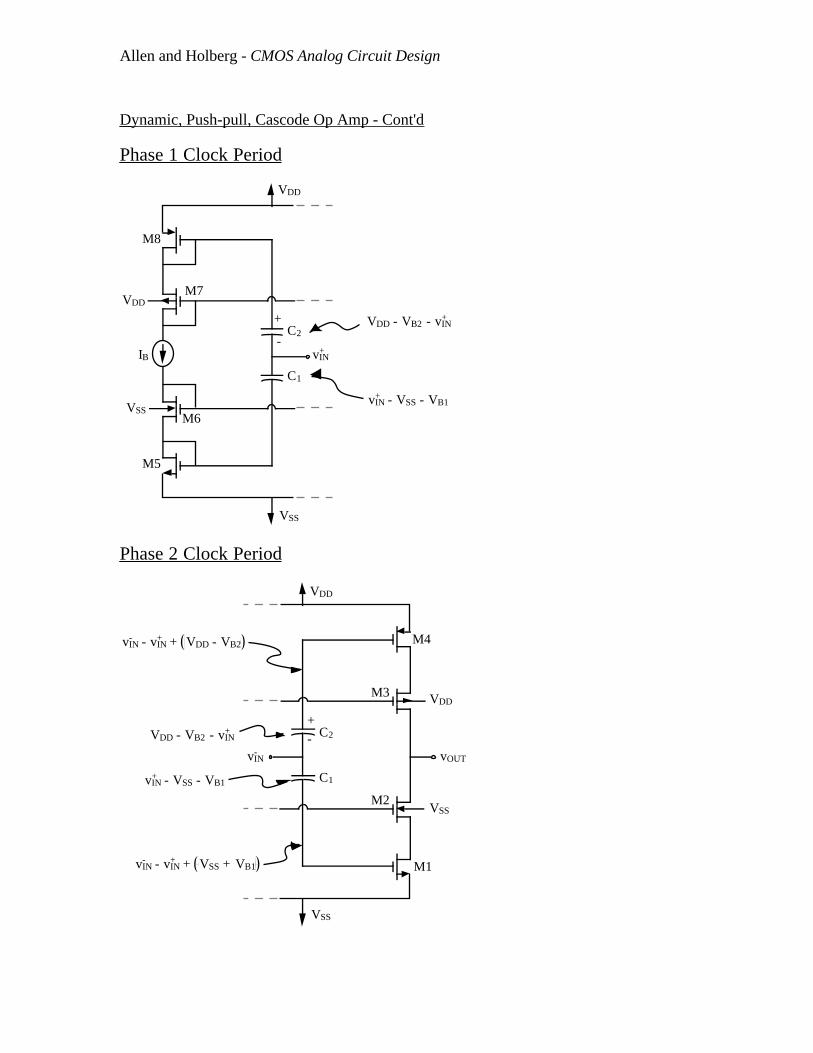
Allen and Holberg - CMOS Analog Circuit Design
Dynamic, Push-pull, Cascode Op Amp - Cont'd
Phase 1 Clock Period
M8
M7
M6
M5
vIN+
C1
C2
IB
VSS
VDD
VDD
VSS
+
-
VDD - VB2 - vIN+
vIN+ - VSS - VB1
Phase 2 Clock Period
M1
M2
M3
M4
C2
+
C1
-vIN
-
vIN- - vIN
+ + VSS + VB1
vIN- - vIN
+ + VDD - VB2
VDD - VB2 - vIN+
vIN+ - VSS - VB1
VSS
VDD
vOUT
VDD
VSS
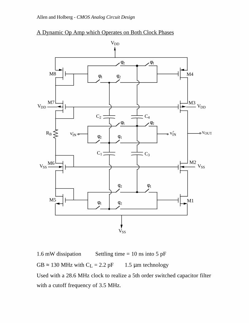
Allen and Holberg - CMOS Analog Circuit Design
A Dynamic Op Amp which Operates on Both Clock Phases
φ1 φ2M8
VDD
M7
C1
C2
VDD
vIN-
M6VSS
M5
M4
M3VDD
vOUTvIN+
M2VSS
M1
VSS
φ1φ2
φ2 φ1
φ1 φ2
C3
C4
φ2
φ2
φ1
φ1
RB
1.6 mW dissipation Settling time = 10 ns into 5 pF
GB ≈ 130 MHz with CL = 2.2 pF 1.5 µm technology
Used with a 28.6 MHz clock to realize a 5th order switched capacitor filter
with a cutoff frequency of 3.5 MHz.
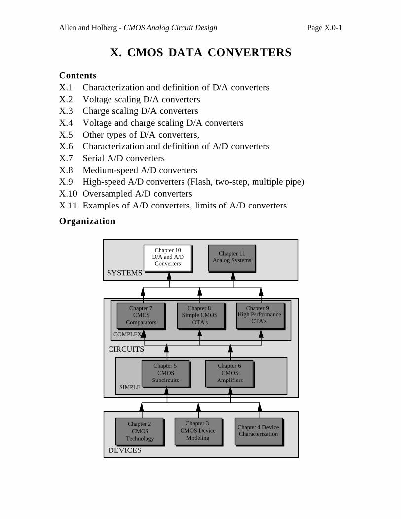
Allen and Holberg - CMOS Analog Circuit Design Page X.0-1
X. CMOS DATA CONVERTERS
ContentsX.1 Characterization and definition of D/A convertersX.2 Voltage scaling D/A convertersX.3 Charge scaling D/A convertersX.4 Voltage and charge scaling D/A convertersX.5 Other types of D/A converters,X.6 Characterization and definition of A/D convertersX.7 Serial A/D convertersX.8 Medium-speed A/D convertersX.9 High-speed A/D converters (Flash, two-step, multiple pipe)X.10 Oversampled A/D convertersX.11 Examples of A/D converters, limits of A/D converters
Organization
DEVICES
SYSTEMS
CIRCUITS
Chapter 2 CMOS
Technology
Chapter 3 CMOS Device
Modeling
Chapter 4 Device Characterization
Chapter 7 CMOS
Comparators
Chapter 8 Simple CMOS
OTA's
Chapter 9 High Performance
OTA's
Chapter 5 CMOS
Subcircuits
Chapter 6 CMOS
Amplifiers
Chapter 10D/A and A/D Converters
Chapter 11Analog Systems
SIMPLE
COMPLEX
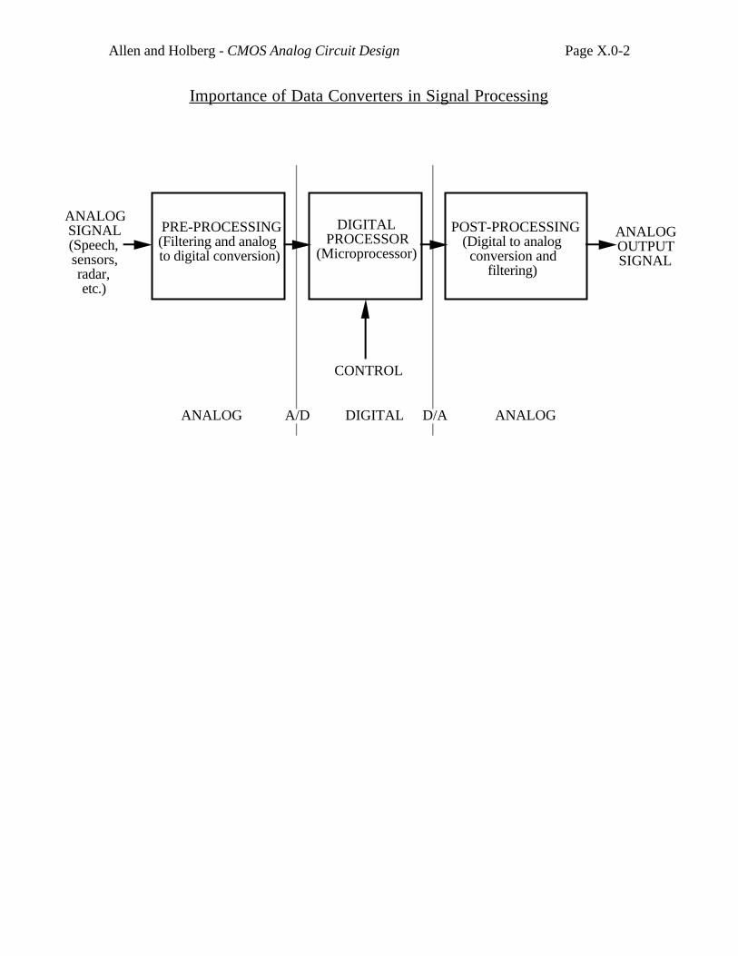
Allen and Holberg - CMOS Analog Circuit Design Page X.0-2
Importance of Data Converters in Signal Processing
PRE-PROCESSING(Filtering and analog to digital conversion)
DIGITAL PROCESSOR
(Microprocessor)
POST-PROCESSING (Digital to analog conversion and
filtering)
ANALOGSIGNAL(Speech,sensors,radar,etc.)
ANALOGOUTPUTSIGNAL
CONTROL
ANALOG A/D D/ADIGITAL ANALOG

Allen and Holberg - CMOS Analog Circuit Design Page X.0-3
A/D and D/A Converters in Data Systems
Analog computerAudio signalsVideo signalsPower sourcesChemical cellsSynchros/resolversPressure cellsThermocouplesStrain gagesBridgesPhotomultiplierEtc.
Multi-plexer
SampleandHold
Analogto
DigitalConverter
DigitalSystem
Transmission linksMagnetic tape recordersComputer memoriesPaper tape recordersReal-time processorComparatorsSystem and process controlsNumerical machine controlsMinicomputersMiroprocessorsEtc.
Reference
Audio systemsControllersActuatorsCRT displaysAnalog recordersAnalog computersHybrid computersAnalog metersTransducersServomotorsX-Y plottersModemsEtc.
Digital to
analog converter
DigitalSystem
Reference
Filter Amplifier
Transmission linksMagnetic tape recordersComputer memoriesPaper tape recordersReal-time processorComparatorsSystem and process controlsNumerical machine controlsMinicomputersMiroprocessorsEtc.
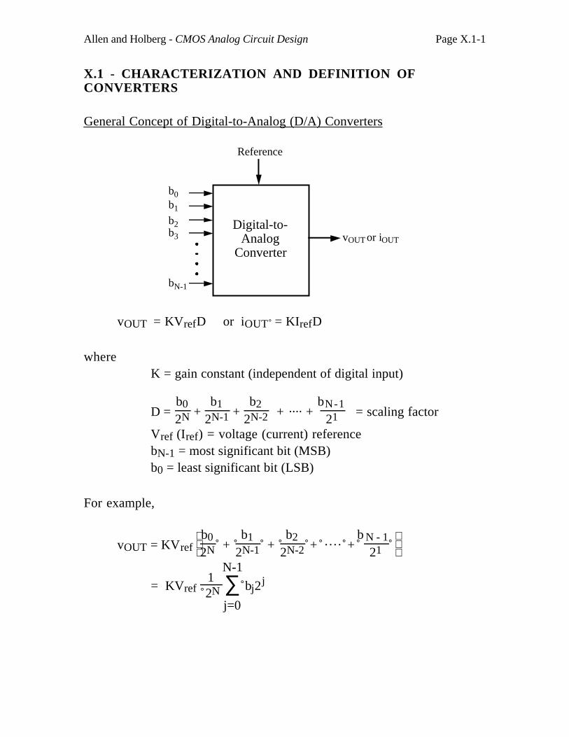
Allen and Holberg - CMOS Analog Circuit Design Page X.1-1
X.1 - CHARACTERIZATION AND DEFINITION OFCONVERTERS
General Concept of Digital-to-Analog (D/A) Converters
Digital-to-Analog
Converter
Reference
vOUT or iOUT
b1
b2b3
b0
bN-1
vOUT = KVrefD or iOUT = KIrefD
whereK = gain constant (independent of digital input)
D = b0
2N + b1
2N-1 + b2
2N-2 + ···· + bN-1
21 = scaling factor
Vref (Iref) = voltage (current) referencebN-1 = most significant bit (MSB)b0 = least significant bit (LSB)
For example,
vOUT = KVref
b0
2N + b1
2N-1 + b2
2N-2 + · · · · + b N - 1
21
= KVref 1
2N ∑j=0
N-1
bj2j
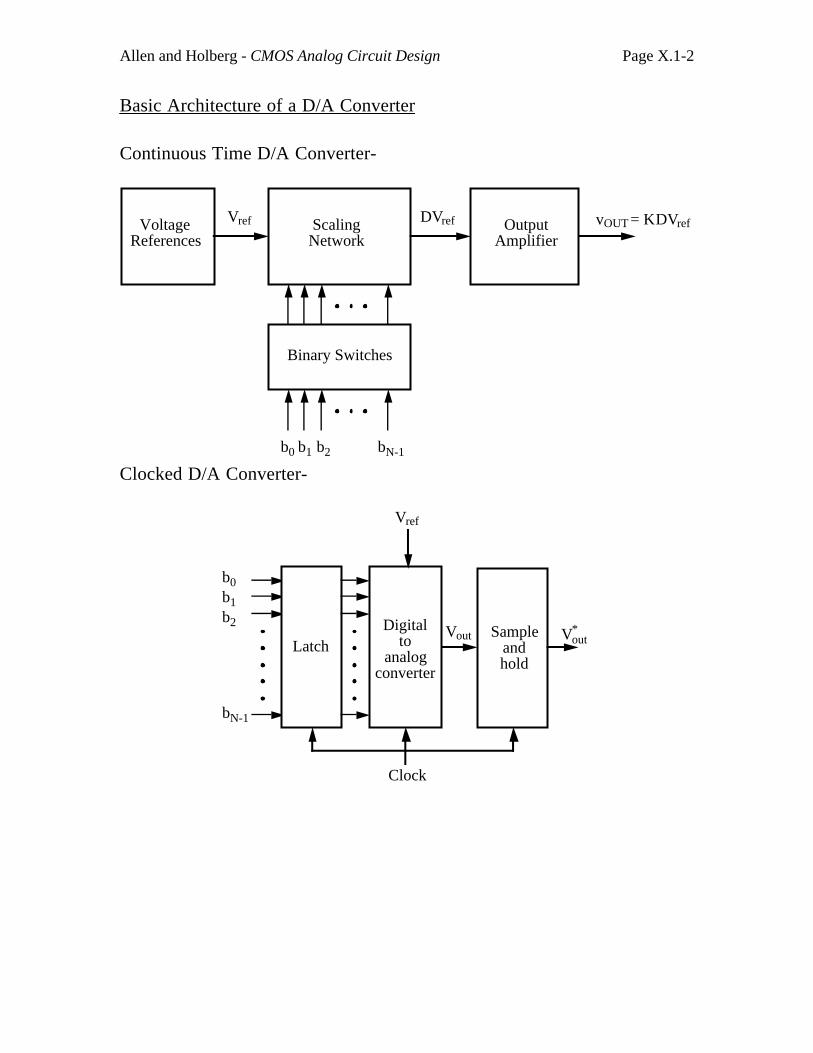
Allen and Holberg - CMOS Analog Circuit Design Page X.1-2
Basic Architecture of a D/A Converter
Continuous Time D/A Converter-
Binary Switches
Scaling Network
Voltage References
Output Amplifier
Vref DVref vOUT = KDVref
b1 b2b0 bN-1
Clocked D/A Converter-
Digital to
analog converter
LatchSample
andhold
Vref
Vout Vout*
Clock
b1b2
b0
bN-1
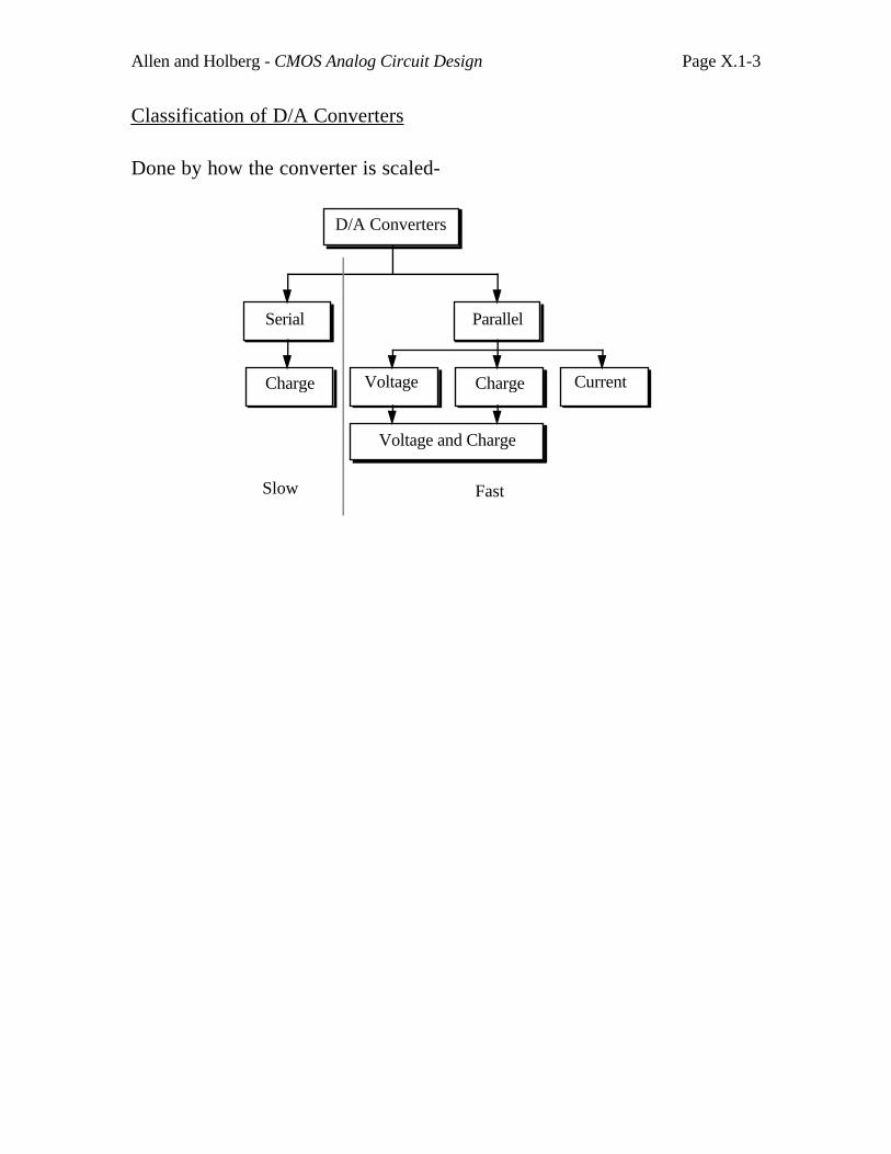
Allen and Holberg - CMOS Analog Circuit Design Page X.1-3
Classification of D/A Converters
Done by how the converter is scaled-
D/A Converters
Serial
Charge
Parallel
ChargeVoltage Current
Voltage and Charge
Slow Fast
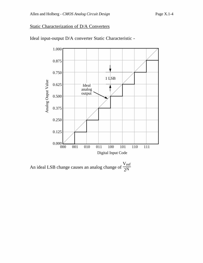
Allen and Holberg - CMOS Analog Circuit Design Page X.1-4
Static Characterization of D/A Converters
Ideal input-output D/A converter Static Characteristic -
0.000
0.125
0.250
0.375
0.500
0.625
0.750
0.875
1.000
000 001 010 011 100 101 110 111
Digital Input Code
Ana
log
Oup
ut V
alue
1 LSB
Idealanalogoutput
An ideal LSB change causes an analog change of Vref
2N
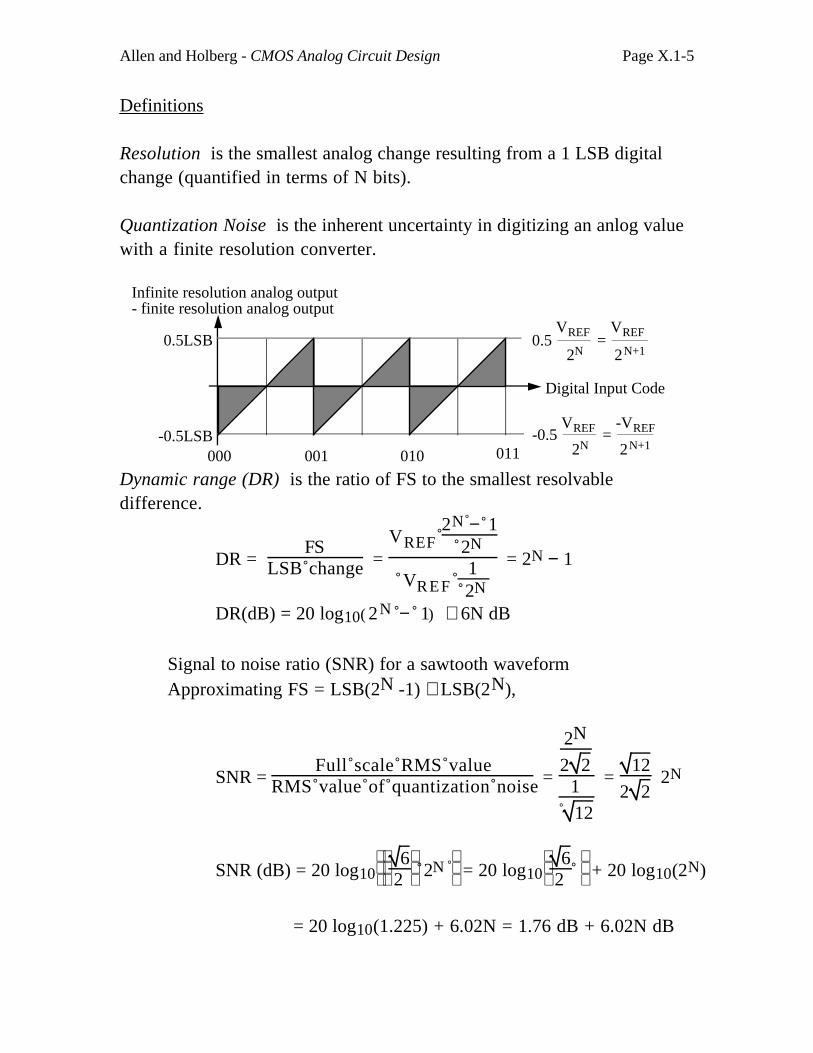
Allen and Holberg - CMOS Analog Circuit Design Page X.1-5
Definitions
Resolution is the smallest analog change resulting from a 1 LSB digitalchange (quantified in terms of N bits).
Quantization Noise is the inherent uncertainty in digitizing an anlog valuewith a finite resolution converter.
Digital Input Code
000 001 010 011
0.5LSB
-0.5LSB
Infinite resolution analog output- finite resolution analog output
0.5VREF
2N =
2N+1
VREF
-0.5VREF
2N =
2N+1
-VREF
Dynamic range (DR) is the ratio of FS to the smallest resolvabledifference.
DR = FS
LSB change = VREF
2N − 1 2N
VREF 1
2N
= 2N − 1
DR(dB) = 20 log10( )2N − 1 ≅ 6N dB
Signal to noise ratio (SNR) for a sawtooth waveformApproximating FS = LSB(2N -1) ≅ LSB(2N),
SNR = Full scale RMS value
RMS value of quantization noise =
2N
2 21
12
= 12
2 2 2N
SNR (dB) = 20 log10
6
2 2N = 20 log10
6
2 + 20 log10(2N)
= 20 log10(1.225) + 6.02N = 1.76 dB + 6.02N dB
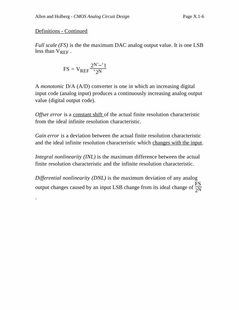
Allen and Holberg - CMOS Analog Circuit Design Page X.1-6
Definitions - Continued
Full scale (FS) is the the maximum DAC analog output value. It is one LSBless than VREF .
FS = VREF 2N − 1
2N
A monotonic D/A (A/D) converter is one in which an increasing digitalinput code (analog input) produces a continuously increasing analog outputvalue (digital output code).
Offset error is a constant shift of the actual finite resolution characteristicfrom the ideal infinite resolution characteristic.
Gain error is a deviation between the actual finite resolution characteristicand the ideal infinite resolution characteristic which changes with the input .
Integral nonlinearity (INL) is the maximum difference between the actualfinite resolution characteristic and the infinite resolution characteristic.
Differential nonlinearity (DNL) is the maximum deviation of any analog
output changes caused by an input LSB change from its ideal change of FS2N
.
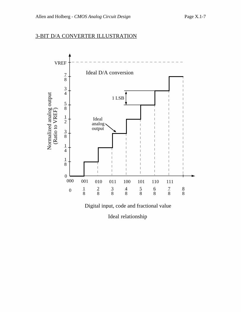
Allen and Holberg - CMOS Analog Circuit Design Page X.1-7
3-BIT D/A CONVERTER ILLUSTRATION
18
14
38
12
58
34
78
VREF
0000 001 010 011 100 101 110 111
0 18
38
58
78
88
28
48
68
Ideal D/A conversion
Idealanalogoutput
1 LSB
Digital input, code and fractional value
Nor
mal
ized
ana
log
outp
ut
(R
atio
to V
RE
F)
Ideal relationship
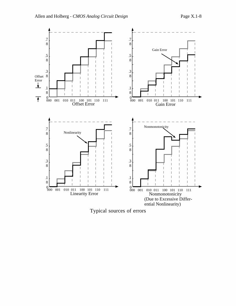
Allen and Holberg - CMOS Analog Circuit Design Page X.1-8
180
38
58
78
Offset Error
OffsetError
000 001 010 011 100 101 110 111
180
38
58
78
Gain Error
Gain Error
000 001 010 011 100 101 110 111
180
38
58
78
Nonmonotonicity(Due to Excessive Differ-ential Nonlinearity)
Nonmonotonicity
000 001 010 011 100 101 110 111
180
38
58
78
Linearity Error
Nonlinearity
000 001 010 011 100 101 110 111
Typical sources of errors
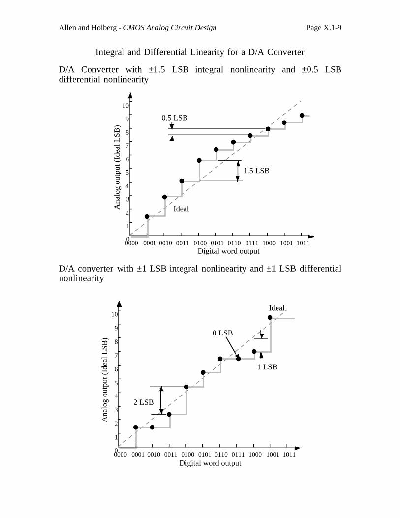
Allen and Holberg - CMOS Analog Circuit Design Page X.1-9
Integral and Differential Linearity for a D/A Converter
D/A Converter with ±1.5 LSB integral nonlinearity and ±0.5 LSBdifferential nonlinearity
0000 0010 0100 0110 1000 10110001 0011 0101 0111 10010
1
2
3
4
5
6
7
8
9
10
0.5 LSB
1.5 LSB
Ideal
Digital word output
Ana
log
outp
ut (
Idea
l LSB
)
D/A converter with ±1 LSB integral nonlinearity and ±1 LSB differentialnonlinearity
0000 0010 0100 0110 1000 10110001 0011 0101 0111 10010
1
2
3
4
5
6
7
8
9
10
2 LSB
0 LSB
Ideal
Digital word output
Ana
log
outp
ut (
Idea
l LSB
)
1 LSB
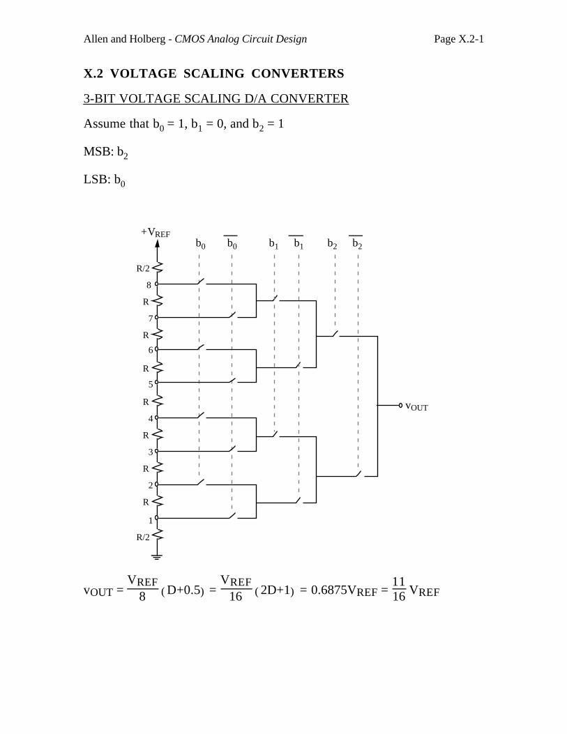
Allen and Holberg - CMOS Analog Circuit Design Page X.2-1
X.2 VOLTAGE SCALING CONVERTERS
3-BIT VOLTAGE SCALING D/A CONVERTER
Assume that b0 = 1, b1 = 0, and b2 = 1
MSB: b2
LSB: b0
1
R/2
+VREF
vOUT
2
3
4
5
6
7
8
R/2
R
R
R
R
R
R
R
b0 b1b0 b1 b2 b2
vOUT = VREF
8 ( )D+0.5 = VREF
16 ( )2D+1 = 0.6875VREF = 1116 VREF
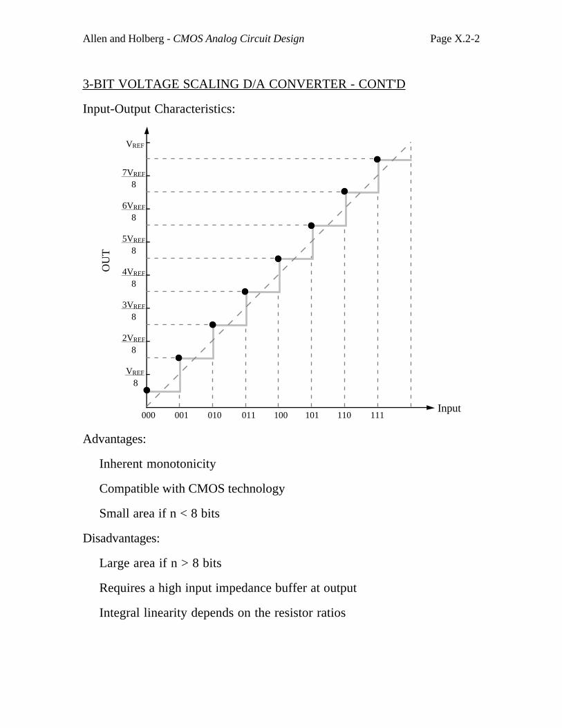
Allen and Holberg - CMOS Analog Circuit Design Page X.2-2
3-BIT VOLTAGE SCALING D/A CONVERTER - CONT'D
Input-Output Characteristics:
VREF
8
2VREF
8
3VREF
8
4VREF
8
5VREF
8
6VREF
8
7VREF
8
VREF
000 001 010 011 100 101 110 111
OU
T
Input
Advantages:
Inherent monotonicity
Compatible with CMOS technology
Small area if n < 8 bits
Disadvantages:
Large area if n > 8 bits
Requires a high input impedance buffer at output
Integral linearity depends on the resistor ratios
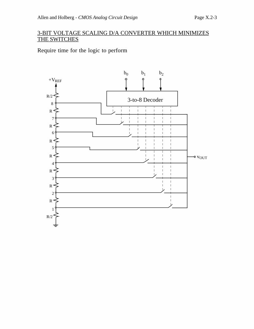
Allen and Holberg - CMOS Analog Circuit Design Page X.2-3
3-BIT VOLTAGE SCALING D/A CONVERTER WHICH MINIMIZES THE SWITCHES
Require time for the logic to perform
1
R/2
+VREF
2
3
4
5
6
7
8
R/2
R
R
R
R
R
R
R
3-to-8 Decoder
vOUT
b0 b1 b2
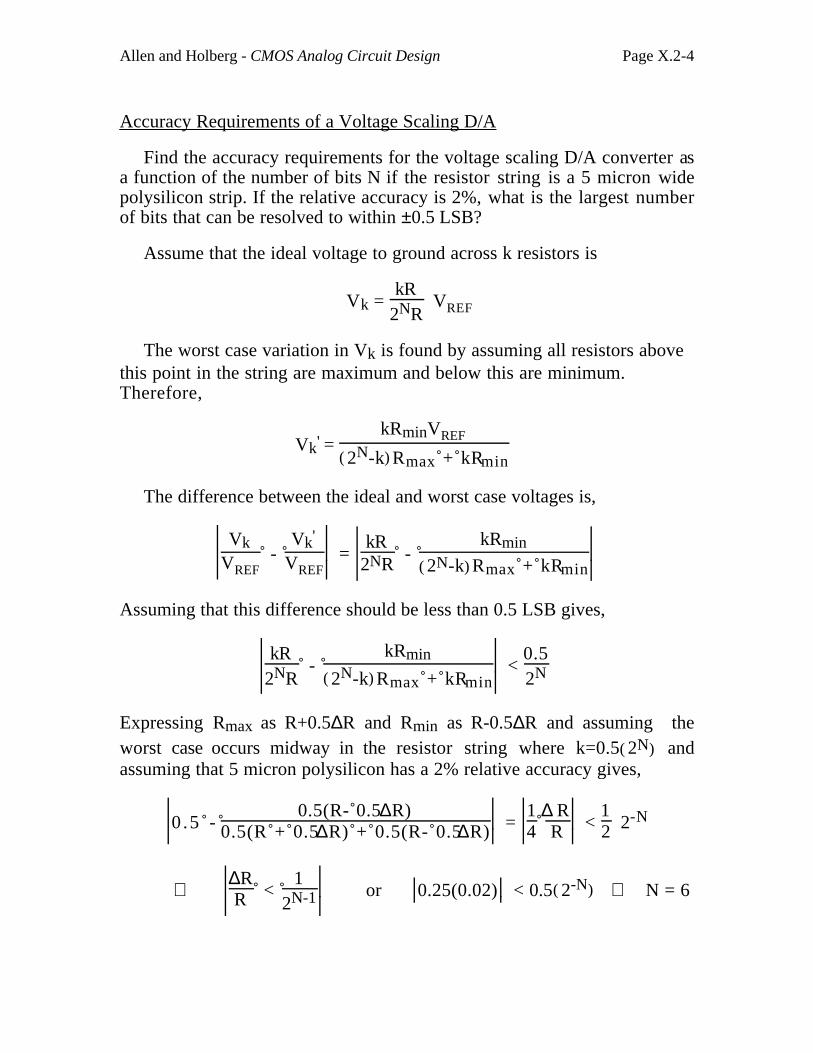
Allen and Holberg - CMOS Analog Circuit Design Page X.2-4
Accuracy Requirements of a Voltage Scaling D/A
Find the accuracy requirements for the voltage scaling D/A converter asa function of the number of bits N if the resistor string is a 5 micron widepolysilicon strip. If the relative accuracy is 2%, what is the largest numberof bits that can be resolved to within ±0.5 LSB?
Assume that the ideal voltage to ground across k resistors is
Vk = kR
2NR VREF
The worst case variation in Vk is found by assuming all resistors abovethis point in the string are maximum and below this are minimum.Therefore,
Vk' = kRminVREF
( )2N-k Rmax + kRmin
The difference between the ideal and worst case voltages is,
VkVREF
- Vk'
VREF =
kR2NR
- kRmin
( )2N-k Rmax + kRmin
Assuming that this difference should be less than 0.5 LSB gives,
kR2NR
- kRmin
( )2N-k Rmax + kRmin <
0.52N
Expressing Rmax as R+0.5∆R and Rmin as R-0.5∆R and assuming theworst case occurs midway in the resistor string where k=0.5( )2N andassuming that 5 micron polysilicon has a 2% relative accuracy gives,
0 .5 - 0.5(R- 0.5∆R)
0.5(R + 0.5∆R) + 0.5(R- 0.5∆R) = 14
∆ RR <
12 2-N
⇒ ∆RR <
12N-1 or 0.25(0.02) < 0.5( )2-N ⇒ N = 6
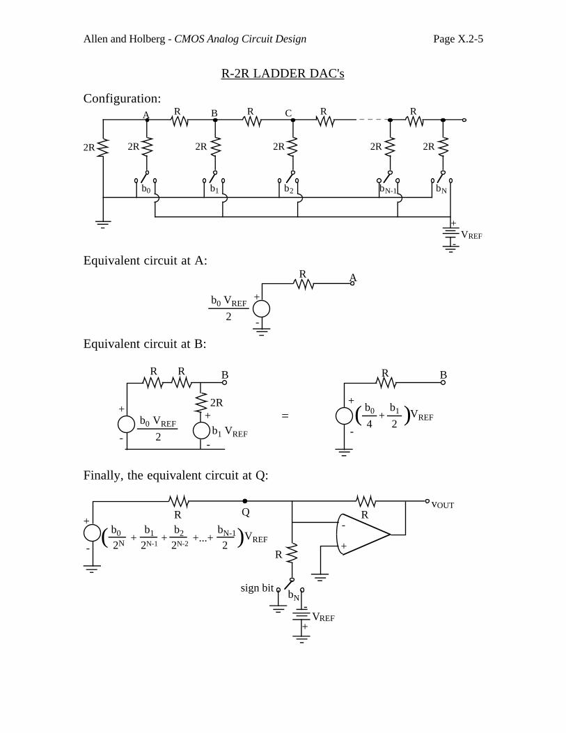
Allen and Holberg - CMOS Analog Circuit Design Page X.2-5
R-2R LADDER DAC's
Configuration:
2R 2R
RRRRA B C
+
-VREF
2R2R2R2R
b0 b1 b2 bN-1 bN
Equivalent circuit at A:
+
-
R A
b0 VREF
2
Equivalent circuit at B:
R B
+
-
+
-
2R
R B
+
-=b0 VREF
2b1 VREF
R
b0
4
b1
2( )+ VREF
Finally, the equivalent circuit at Q:
+
-R
-
+
RR Q
-
+VREF
sign bit
vOUT
b0
2N
b1( )+ VREFb2+
2N-1 2N-2+...+
bN-1
2
bN
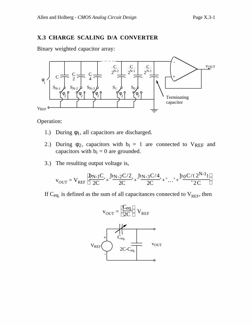
Allen and Holberg - CMOS Analog Circuit Design Page X.3-1
X.3 CHARGE SCALING D/A CONVERTER
Binary weighted capacitor array:
φ2
C2N-1
C2N-1
C2N-2
C4
C2
φ2
φ2
φ2
φ2
C
VREF
-
+φ1
vOUT
Terminatingcapacitor
S0S1SN-3SN-2SN-1
Operation:
1.) During φ1, all capacitors are discharged.
2.) During φ2, capacitors with bi = 1 are connected to VREF andcapacitors with bi = 0 are grounded.
3.) The resulting output voltage is,
vOUT = VREF
bN-1C
2C + bN-2C/2
2C + bN-3C/4
2C + ... + b0C/( )2N-1
2C
If Ceq. is defined as the sum of all capacitances connected to VREF, then
vOUT =
Ceq.
2C VREF
vOUT
Ceq.
2C-Ceq.
+
-
VREF
Allen and Holberg - CMOS Analog Circuit Design Page X.3-2
Other Versions of the Charge Scaling D/A Converter
Bipolar Operation:
Charge all capacitors to VREF. If bi = 1, connect the capacitor toground, if bi = 0, connect the capacitor to VREF.
Will require an extra bit to decide whether to connect the capacitorsinitially to ground or to VREF.
Four-Quadrant Operation:
If VREF can have ±values, then a full, four quadrant DAC can beobtained.
Multiplying DAC:
If VREF is an analog signal (sampled and held), then the output is theproduct of a digital word and an analog signal and is called a multiplyingDAC (MDAC).
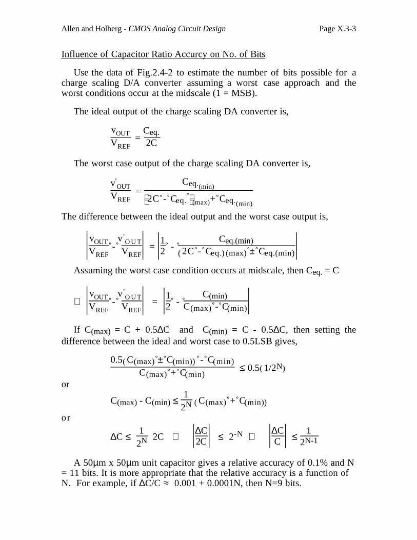
Allen and Holberg - CMOS Analog Circuit Design Page X.3-3
Influence of Capacitor Ratio Accurcy on No. of Bits
Use the data of Fig.2.4-2 to estimate the number of bits possible for acharge scaling D/A converter assuming a worst case approach and theworst conditions occur at the midscale (1 = MSB).
The ideal output of the charge scaling DA converter is,
vOUT
VREF =
Ceq.2C
The worst case output of the charge scaling DA converter is,
v'OUT
VREF =
Ceq.(min)
2C - Ceq. (max)+ Ceq.(min)
The difference between the ideal output and the worst case output is,
vOUT
VREF -
v'O U T
VREF =
12 -
Ceq.(min)
( )2C - Ceq. (max) ± Ceq.(min)
Assuming the worst case condition occurs at midscale, then Ceq. = C
∴ vOUT
VREF -
v'O U T
VREF =
12 -
C(min)C(max) - C(min)
If C(max) = C + 0.5∆C and C(min) = C - 0.5∆C, then setting thedifference between the ideal and worst case to 0.5LSB gives,
0.5( )C(max) ± C(min) - C(min)
C(max) + C(min) ≤ 0.5( )1/2N
or
C(max) - C(min) ≤ 1
2N ( )C(max) + C(min)
or
∆C ≤ 1
2N 2C ⇒ ∆C2C ≤ 2-N ⇒
∆CC ≤
12N-1
A 50µm x 50µm unit capacitor gives a relative accuracy of 0.1% and N= 11 bits. It is more appropriate that the relative accuracy is a function ofN. For example, if ∆C/C ≈ 0.001 + 0.0001N, then N=9 bits.
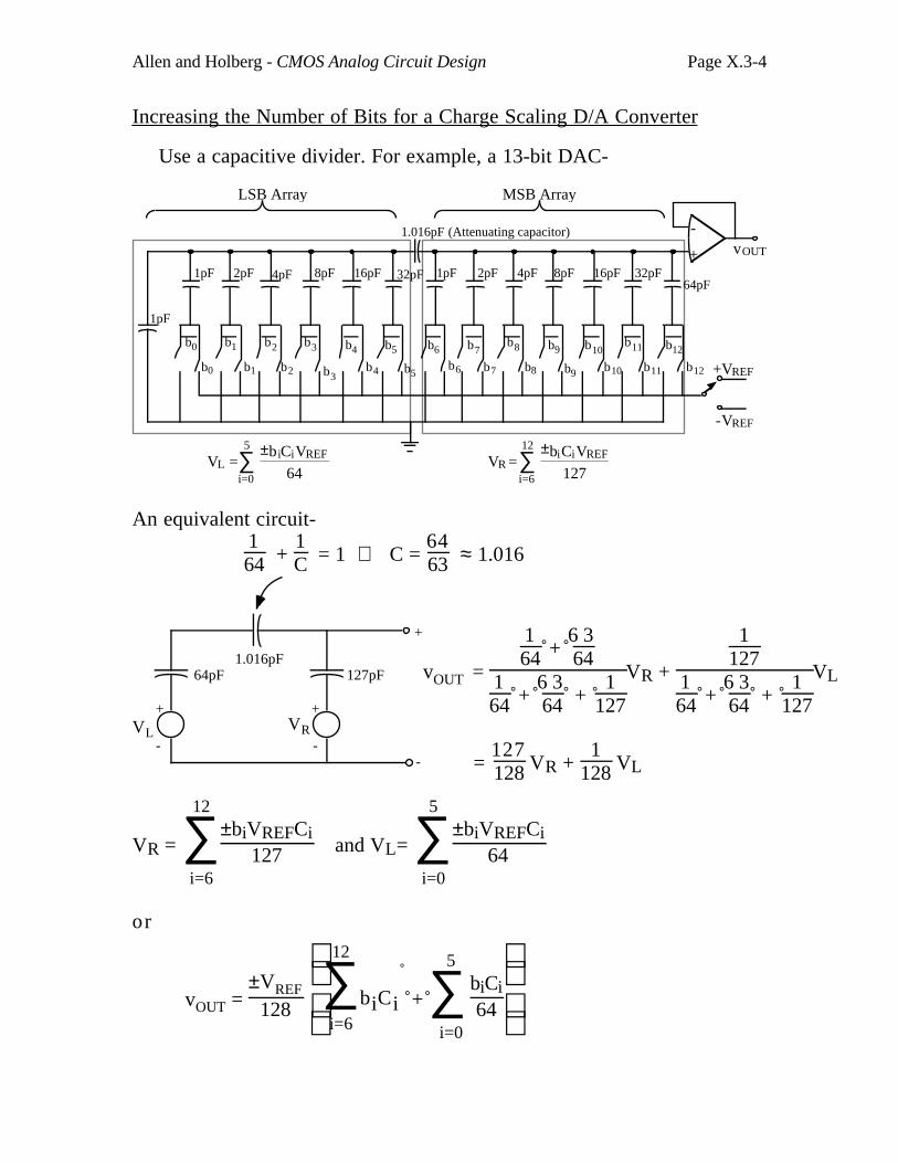
Allen and Holberg - CMOS Analog Circuit Design Page X.3-4
Increasing the Number of Bits for a Charge Scaling D/A Converter
Use a capacitive divider. For example, a 13-bit DAC-
-VREF
+VREF
vOUT
-
+
64pF32pF16pF8pF4pF2pF1pF
1.016pF
32pF16pF8pF4pF2pF1pF
1pF
(Attenuating capacitor)
LSB Array MSB Array
VL =±biCiVREF
64∑i=0
5
VR =±biCiVREF
127∑i=6
12
b0 b1 b2 b3b4 b5
b6
b7
b8 b9 b10
b11 b12b0 b1 b2 b3 b4 b5 b6
b7
b8 b9 b10
b11 b12
An equivalent circuit-
164 +
1C = 1 ⇒ C =
6463 ≈ 1.016
+
-
+
-
64pF1.016pF
127pF
+
-
VRVL
VR = ∑i=6
12±biVREFCi
127 and VL= ∑i=0
5±biVREFCi
64
or
vOUT = ±VREF
128
∑
i=6
12
biCi
+ ∑i=0
5biCi64
vOUT =
164 +
6 364
164 +
6 364 +
1127
VR +
1127
164 +
6 364 +
1127
VL
= 127128 VR +
1128 VL
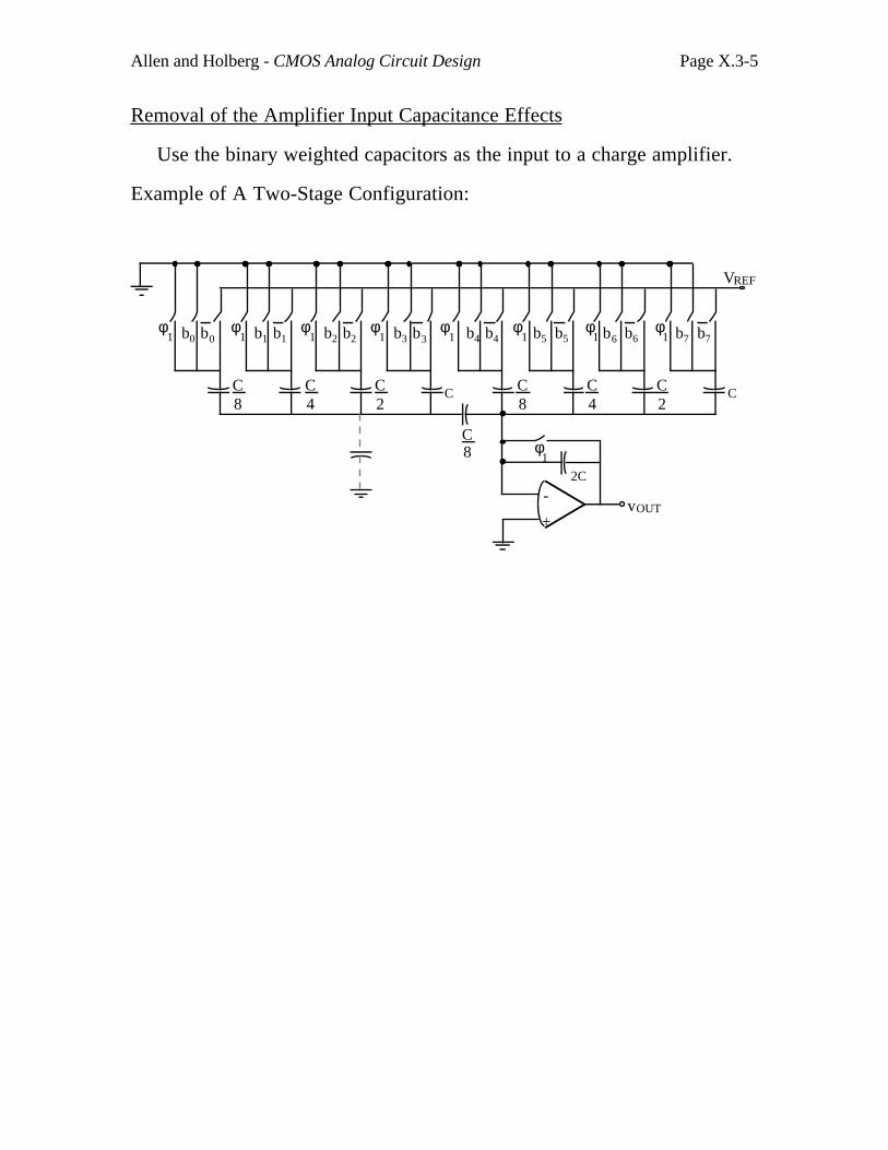
Allen and Holberg - CMOS Analog Circuit Design Page X.3-5
Removal of the Amplifier Input Capacitance Effects
Use the binary weighted capacitors as the input to a charge amplifier.
Example of A Two-Stage Configuration:
vOUT-
+
2C
VREF
φ1
φ1
φ1
φ1
φ1
φ1
φ1
φ1
φ1
CC2
C4
C8
CC2
C4
C8
C8
b0 b0 b1 b1 b2 b2 b3 b3 b4 b4 b5 b5 b6 b6 b7 b7
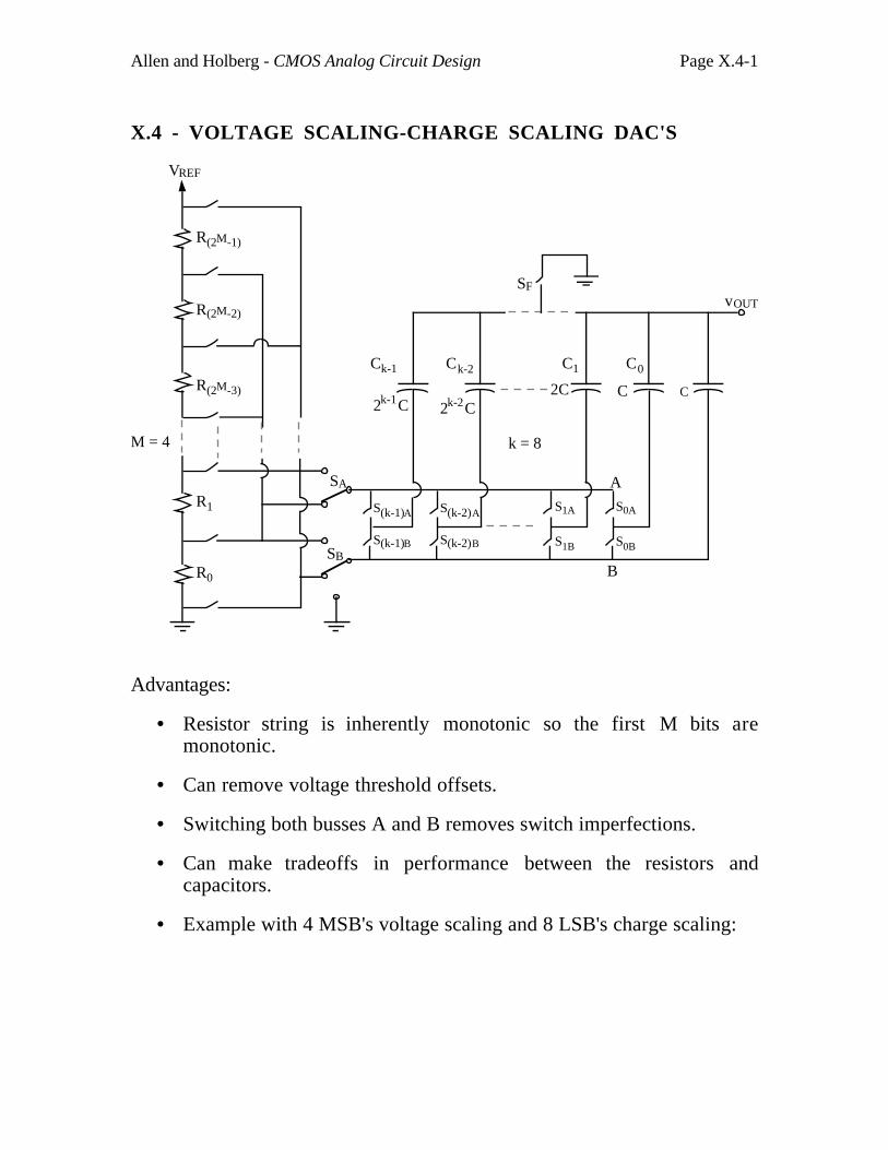
Allen and Holberg - CMOS Analog Circuit Design Page X.4-1
X.4 - VOLTAGE SCALING-CHARGE SCALING DAC'S
vOUT
C
k = 8
2k-1C
SA
SB
2k-2C2C C
A
B
SF
M = 4
VREF
R(2M-1)
R0
R1
R(2M-2)
R(2M-3)
C0C1Ck-1
S0A
S0B
S1A
S1B
S(k-2)A
S(k-2)B
S(k-1)A
S(k-1)B
Ck-2
Advantages:
• Resistor string is inherently monotonic so the first M bits aremonotonic.
• Can remove voltage threshold offsets.
• Switching both busses A and B removes switch imperfections.
• Can make tradeoffs in performance between the resistors andcapacitors.
• Example with 4 MSB's voltage scaling and 8 LSB's charge scaling:
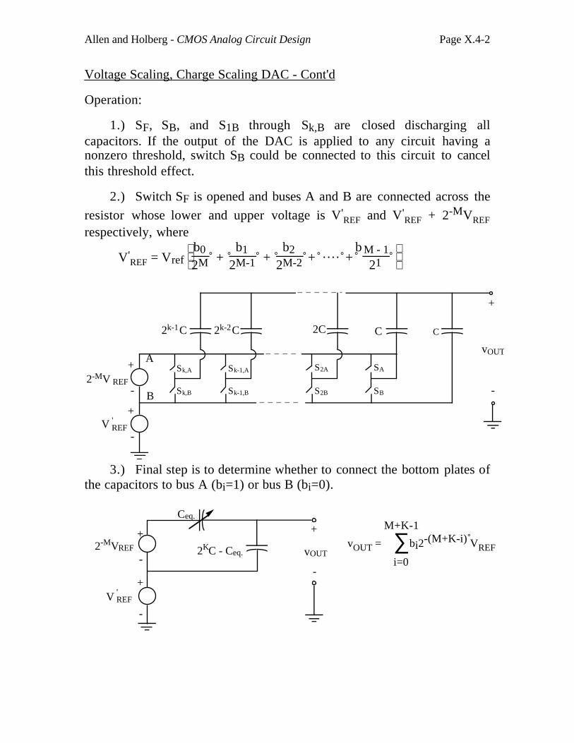
Allen and Holberg - CMOS Analog Circuit Design Page X.4-2
Voltage Scaling, Charge Scaling DAC - Cont'd
Operation:
1.) SF, SB, and S1B through Sk,B are closed discharging allcapacitors. If the output of the DAC is applied to any circuit having anonzero threshold, switch SB could be connected to this circuit to cancelthis threshold effect.
2.) Switch SF is opened and buses A and B are connected across the
resistor whose lower and upper voltage is V'REF and V'
REF + 2-MVREF
respectively, where
V'REF = Vref
b0
2M + b1
2M-1 + b2
2M-2 + · · · · + b M - 1
21
vOUT
Sk,B
Sk,A Sk-1,A
Sk-1,B S2B
S2A
2C C2k-1C 2k-2C C
SA
SB
A
B
+
+
-
-V REF
'
2-MV REF
+
-
3.) Final step is to determine whether to connect the bottom plates ofthe capacitors to bus A (bi=1) or bus B (bi=0).
-
+
-
Ceq.
2KC - Ceq. vOUT
+
-2-MVREF
+V REF
'
vOUT = ∑i=0
M+K-1
bi2-(M+K-i) VREF
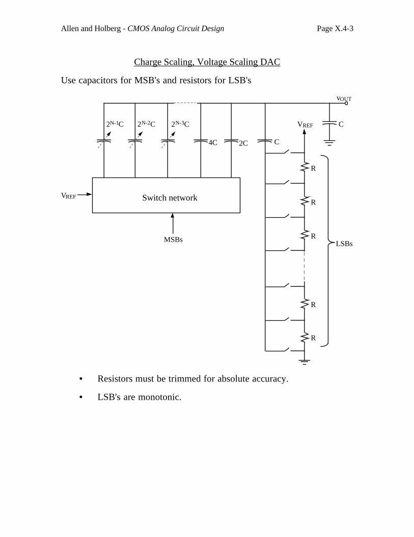
Allen and Holberg - CMOS Analog Circuit Design Page X.4-3
Charge Scaling, Voltage Scaling DAC
Use capacitors for MSB's and resistors for LSB's
VREF
R
R
R
R
R
C4C 2C
MSBs
Switch networkVREF
vOUT
LSBs
C2N-1C 2N-2C 2N-3C
• Resistors must be trimmed for absolute accuracy.
• LSB's are monotonic.
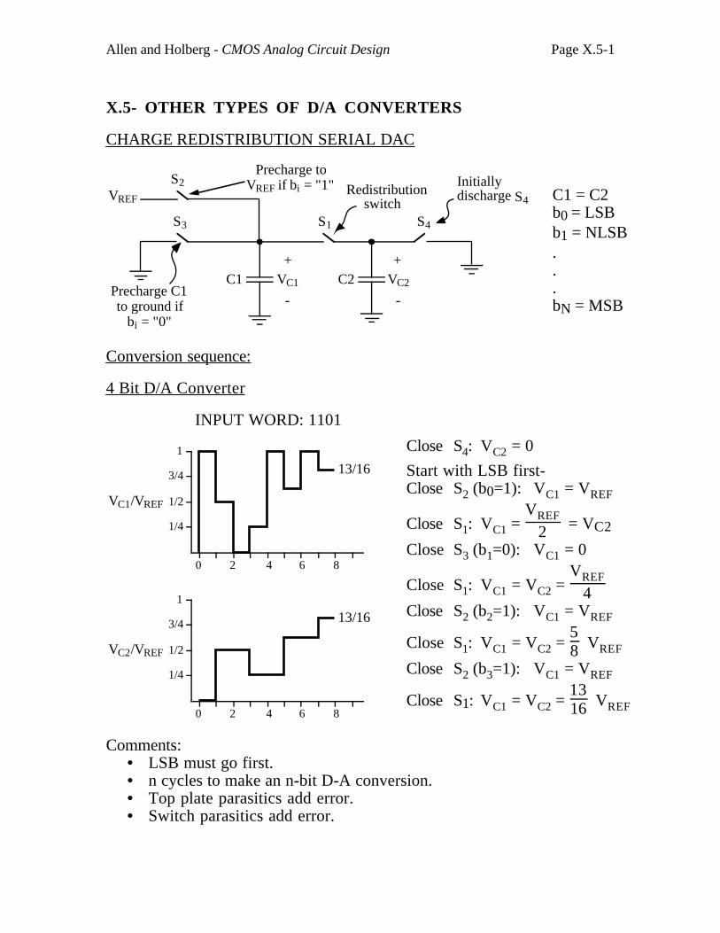
Allen and Holberg - CMOS Analog Circuit Design Page X.5-1
X.5- OTHER TYPES OF D/A CONVERTERS
CHARGE REDISTRIBUTION SERIAL DAC
C1 C2+
-
VC1
+
-
VC2
S3 S1 S4
Precharge C1 to ground if
bi = "0"
Precharge toVREF if bi = "1"
VREF
S2Redistribution switch
Initiallydischarge S4
Conversion sequence:
4 Bit D/A Converter
INPUT WORD: 1101
0 2 4 86
1/4
1/2
3/4
1
VC1/VREF
13/16
0 2 4 86
1/4
1/2
3/4
1
VC2/VREF
13/16
Comments:• LSB must go first.• n cycles to make an n-bit D-A conversion.• Top plate parasitics add error.• Switch parasitics add error.
C1 = C2b0 = LSBb1 = NLSB...bN = MSB
Close S4: VC2 = 0
Start with LSB first-Close S2 (b0=1): VC1 = VREF
Close S1: VC1 = VREF
2 = VC2
Close S3 (b1=0): VC1 = 0
Close S1: VC1 = VC2 = VREF
4
Close S2 (b2=1): VC1 = VREF
Close S1: VC1 = VC2 = 58 VREF
Close S2 (b3=1): VC1 = VREF
Close S1: VC1 = VC2 = 1316 VREF
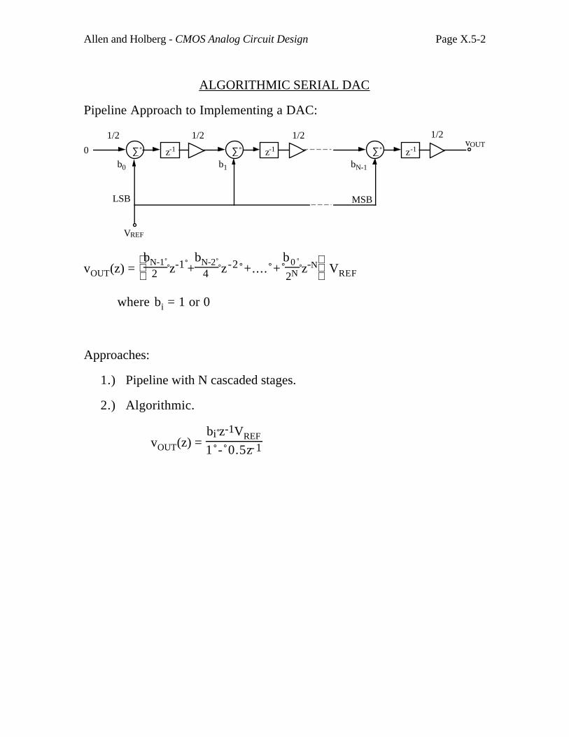
Allen and Holberg - CMOS Analog Circuit Design Page X.5-2
ALGORITHMIC SERIAL DAC
Pipeline Approach to Implementing a DAC:
∑ z-1 ∑ ∑
MSB
vOUT
VREF
LSB
0
1/2
z-1
1/2
z-1
1/2
bN-1b0 b1
1/2
vOUT(z) =
bN-1
2 z-1 +bN-2
4 z-2 +.... + b0
2N z-N VREF
where bi = 1 or 0
Approaches:
1.) Pipeline with N cascaded stages.
2.) Algorithmic.
vOUT(z) = bi z-1VREF
1 - 0.5z-1
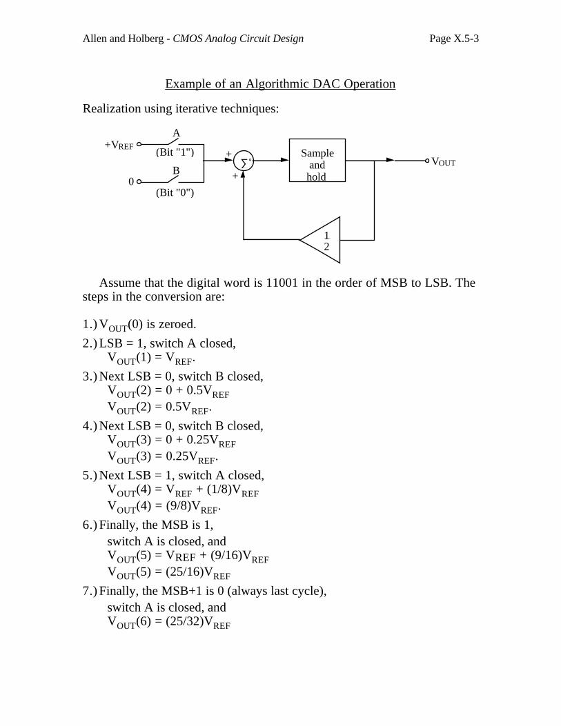
Allen and Holberg - CMOS Analog Circuit Design Page X.5-3
Example of an Algorithmic DAC Operation
Realization using iterative techniques:
Sample and hold
∑
+VREF+
+VOUT
A
B
(Bit "0")
(Bit "1")
12
0
Assume that the digital word is 11001 in the order of MSB to LSB. Thesteps in the conversion are:
1.) VOUT(0) is zeroed.
2.) LSB = 1, switch A closed,VOUT(1) = VREF.
3.) Next LSB = 0, switch B closed,VOUT(2) = 0 + 0.5VREF
VOUT(2) = 0.5VREF.
4.) Next LSB = 0, switch B closed,VOUT(3) = 0 + 0.25VREF
VOUT(3) = 0.25VREF.
5.) Next LSB = 1, switch A closed,VOUT(4) = VREF + (1/8)VREF
VOUT(4) = (9/8)VREF.
6.) Finally, the MSB is 1,switch A is closed, andVOUT(5) = VREF + (9/16)VREF
VOUT(5) = (25/16)VREF
7.) Finally, the MSB+1 is 0 (always last cycle),switch A is closed, andVOUT(6) = (25/32)VREF
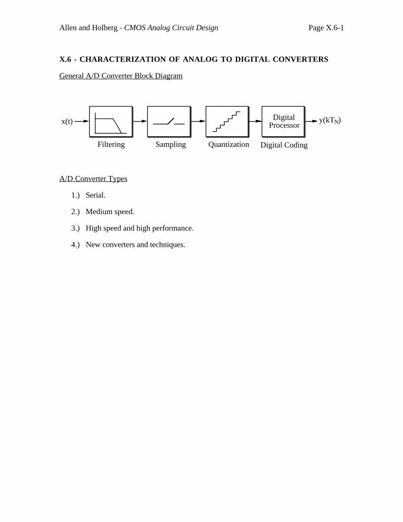
Allen and Holberg - CMOS Analog Circuit Design Page X.6-1
X.6 - CHARACTERIZATION OF ANALOG TO DIGITAL CONVERTERS
General A/D Converter Block Diagram
x(t)
Filtering Sampling Quantization
DigitalProcessor
Digital Coding
y(kTN)
A/D Converter Types
1.) Serial.
2.) Medium speed.
3.) High speed and high performance.
4.) New converters and techniques.
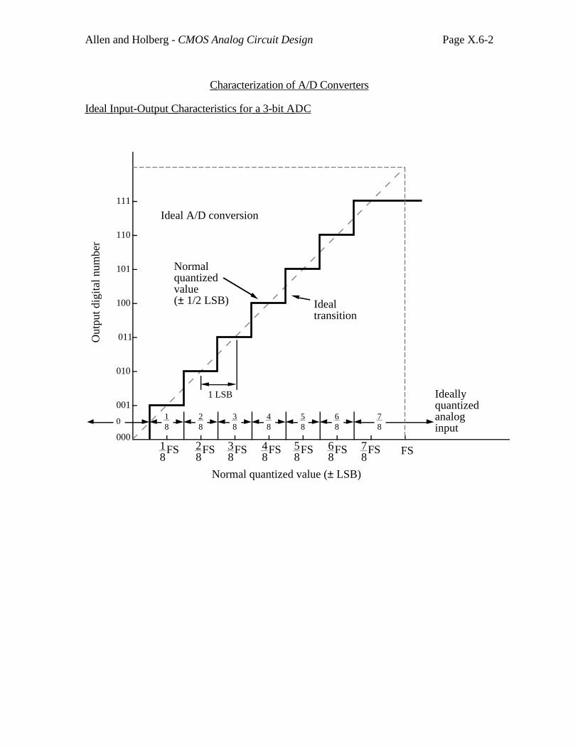
Allen and Holberg - CMOS Analog Circuit Design Page X.6-2
Characterization of A/D Converters
Ideal Input-Output Characteristics for a 3-bit ADC
000
001
010
011
100
101
110
111
18
FS 28
FS 38
FS 48
FS 58
FS 68
FS 78
FS FS
1 LSB
Ideal A/D conversion
Normalquantizedvalue(± 1/2 LSB) Ideal
transition
Normal quantized value (± LSB)
Ideallyquantizedanaloginput
0 18
28
38
48
58
68
78
Out
put d
igita
l num
ber

Allen and Holberg - CMOS Analog Circuit Design Page X.6-3
Nonideal Characteristics of A/D Converters
111
110
101
100
011
010
001
000
Dig
ital o
utpu
t cod
e
14
FS 12
FS 34
FS FS
Analog input value
111
110
101
100
011
010
001
000
Dig
ital o
utpu
t cod
e14
FS 12
FS 34
FS FS
Analog input value
111
110
101
100
011
010
001
000
Dig
ital o
utpu
t cod
e
14
FS 12
FS 34
FS FS
Analog input value
111
110
101
100
011
010
001
000
Dig
ital o
utpu
t cod
e
14
FS 12
FS 34
FS FS
Analog input value
Ideal
Offseterror
Offset Error Scale factor (gain) error
Integral Nonlinearity Differential Nonlinearity
Ideal
Gain error
Ideal
Missedcodes due to excessive differentialnonlinearity
Ideal
Nonlinearity
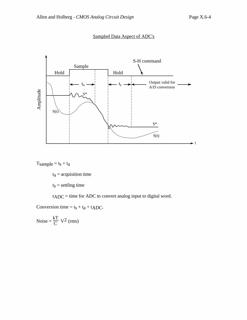
Allen and Holberg - CMOS Analog Circuit Design Page X.6-4
Sampled Data Aspect of ADC's
HoldSample
Hold
Am
plitu
de
tsta
S(t)
S*
S*
S(t)
t
Output valid forA/D conversion
S-H command
Tsample = ts + ta
ta = acquisition time
ts = settling time
tADC = time for ADC to convert analog input to digital word.
Conversion time = ts + ta + tADC.
Noise = kTC V2 (rms)
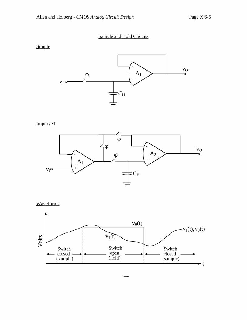
Allen and Holberg - CMOS Analog Circuit Design Page X.6-5
Sample and Hold Circuits
Simple
-
+A1
vO
CH
vI
φ
Improved
-
+A1
vO
CHvI
φ-
+
φA2
φ
Waveforms
v1(t),v0(t)
t
Switch closed(sample)
Switch open(hold)
v1(t)
v0(t)
Switch closed(sample)
Vol
ts
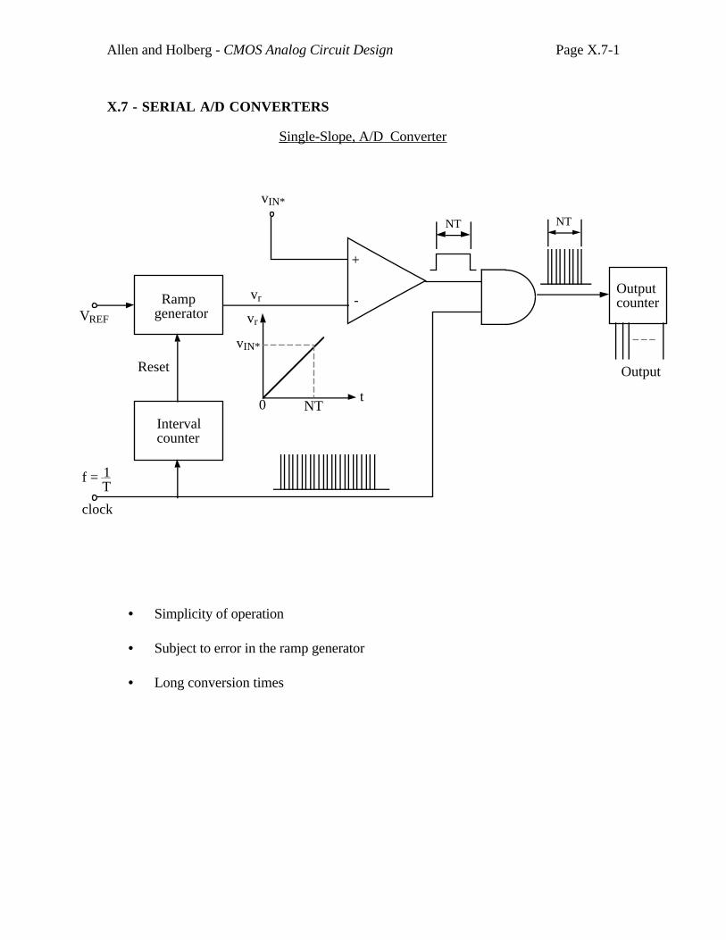
Allen and Holberg - CMOS Analog Circuit Design Page X.7-1
X.7 - SERIAL A/D CONVERTERS
Single-Slope, A/D Converter
• Simplicity of operation
• Subject to error in the ramp generator
• Long conversion times
VREF
+
-vr
t
vr
vIN*
NT0
Rampgenerator
Intervalcounter
Reset
Outputcounter
Output
NT
f = 1T
clock
vIN*
NT
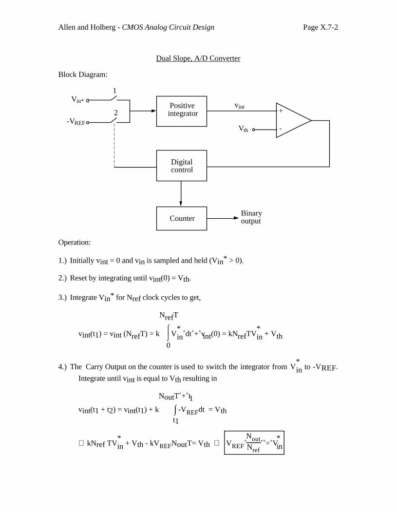
Allen and Holberg - CMOS Analog Circuit Design Page X.7-2
Dual Slope, A/D Converter
Block Diagram:
Positiveintegrator
Digitalcontrol
Counter
+
-
vint
Vth
Binaryoutput
1
2
Vin*
-VREF
Operation:
1.) Initially vint = 0 and vin is sampled and held (Vin* > 0).
2.) Reset by integrating until vint(0) = Vth.
3.) Integrate Vin* for Nref clock cycles to get,
vint(t1) = vint (NrefT) = k ⌡⌠
0
NrefT
V*in dt + vint(0) = kNrefTV
*in + Vth
4.) The Carry Output on the counter is used to switch the integrator from V*in to -VREF.
Integrate until vint is equal to Vth resulting in
vint(t1 + t2) = vint(t1) + k ⌡⌠t1
NoutT + t1
-VREFdt = Vth
∴ kNref TV*in + Vth - kVREFNoutT= Vth ⇒ VREF
NoutNref
= V*in
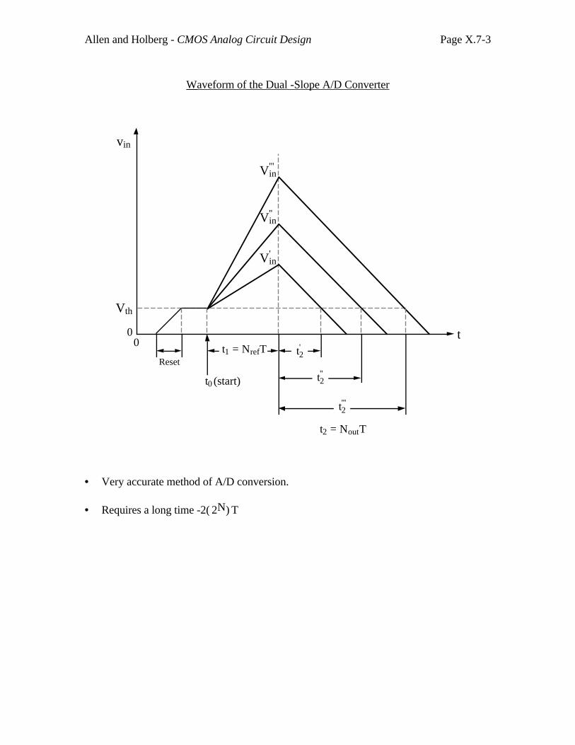
Allen and Holberg - CMOS Analog Circuit Design Page X.7-3
Waveform of the Dual -Slope A/D Converter
vin
t
Vth
00
Vin'''
Vin''
Vin'
t2'
t2''
t2'''
t2 = NoutT
t0 (start)
t1 = NrefTReset
• Very accurate method of A/D conversion.
• Requires a long time -2( )2N T

Allen and Holberg - CMOS Analog Circuit Design Page X.7-4
Switched Capacitor Integrators
Noninverting:
-
+
+
-
v1(t)
φ1
φ1φ2
φ2
C1 C2
+
-
v2(t) fsignal << fclock
Operation:
Assume non-overlapping clocks φ1 and φ2. During φ1, C1 is charged to v1[ ]( )n-1 T
giving a charge of q1[ ]( )n-1 T on C1. During φ2, the charge across C1 is added to the charge
already on C2 which is q2[ ]( )n-1 T resulting in a new charge across C2 designated as
q2( )nT . The charge equation can be written as,
q2( )nT = q2[ ]( )n-1 T + q1[ ]( )n-1 T or
C2v2( )nT = C2 v2 [ ]( )n-1 T + C1 v1 [ ]( )n-1 T
Using z-domain notation gives
C2v2(z) = C2z-1v2(z) + C1z-1v1(z)
or
H(z) = v2(z)v1(z) =
C1C2
z-1
1 - z-1
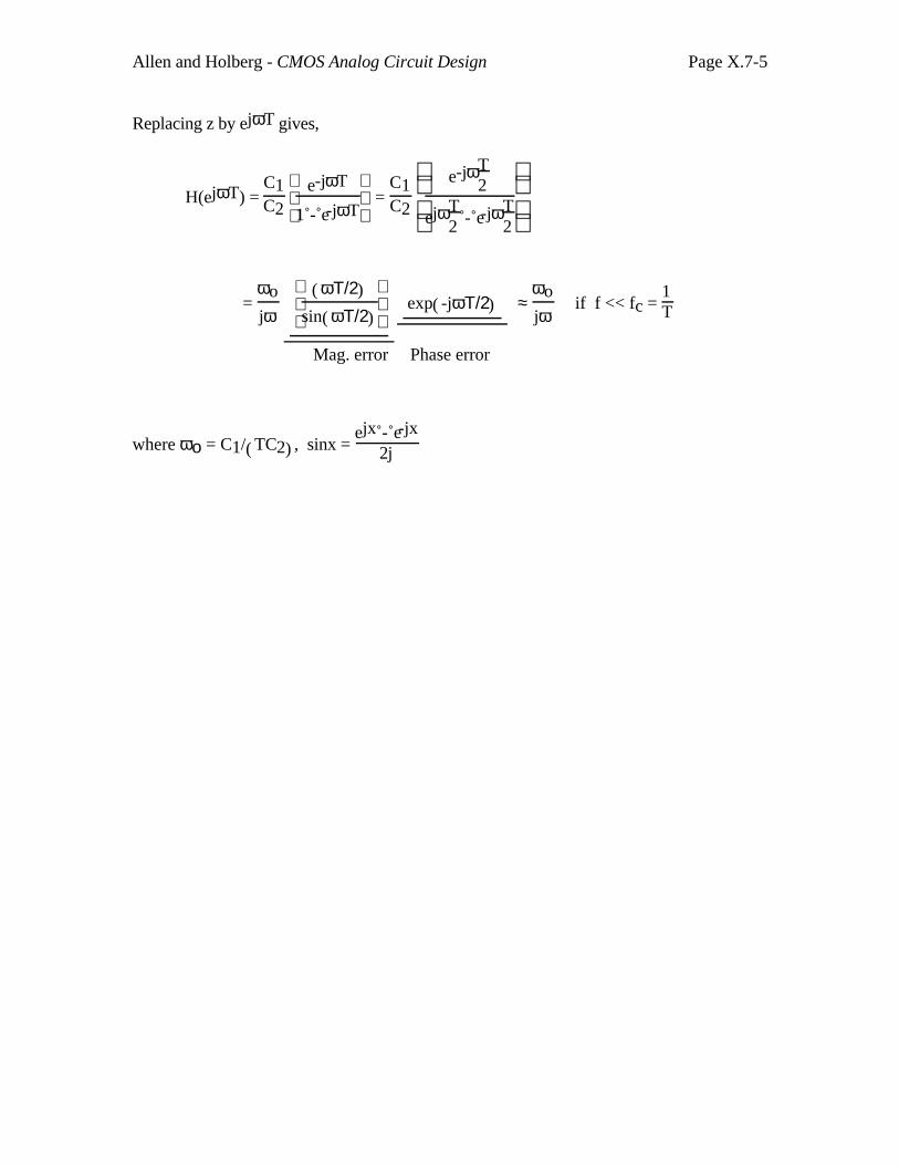
Allen and Holberg - CMOS Analog Circuit Design Page X.7-5
Replacing z by ejωT gives,
H(ejωT) = C1C2
e-jωT
1 - e-jωT =
C1C2
e-jωT
2
ejωT2 - e-jωT
2
= ωo
jω
( )ωΤ/2
sin( )ωΤ/2exp( )-jωΤ/2 ≈
ωo
jω if f << fc =
1T
Mag. error Phase error
where ωο = C1/( )TC2 , sinx = ejx - e-jx
2j
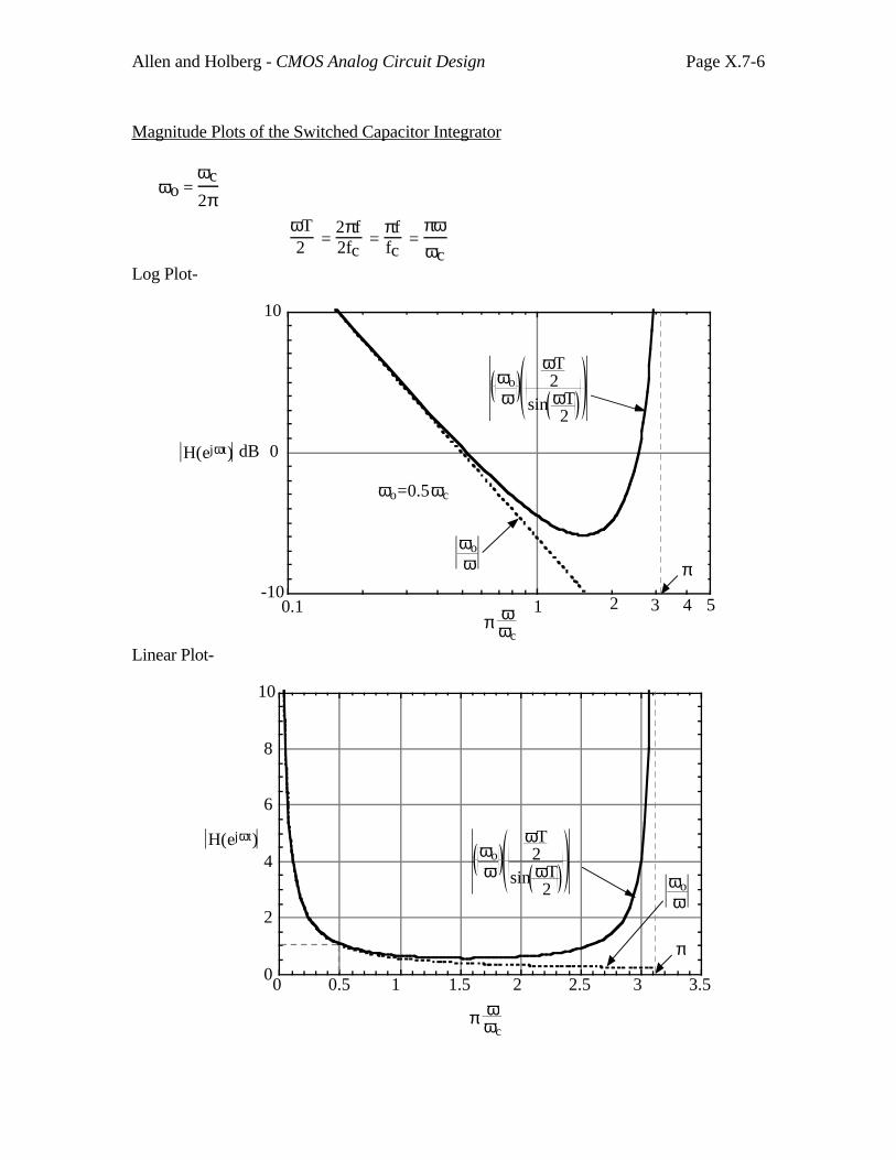
Allen and Holberg - CMOS Analog Circuit Design Page X.7-6
Magnitude Plots of the Switched Capacitor Integrator
ωo = ωc
2π
ωT2 =
2πf2fc
= πffc
= πωωc
Log Plot-
-10
0
10
0.1 1 2 3 4 5ωωc
dB
ωo=0.5ωc
ωoω
ωoω
ωT2
sin ωT2
π
H(ejωt)
π
Linear Plot-
0
2
4
6
8
10
0 0.5 1 1.5 2 2.5 3 3.5
ωωc
π
ωoω
ωoω
ωT2
sin ωT2
H(ejωt)
π
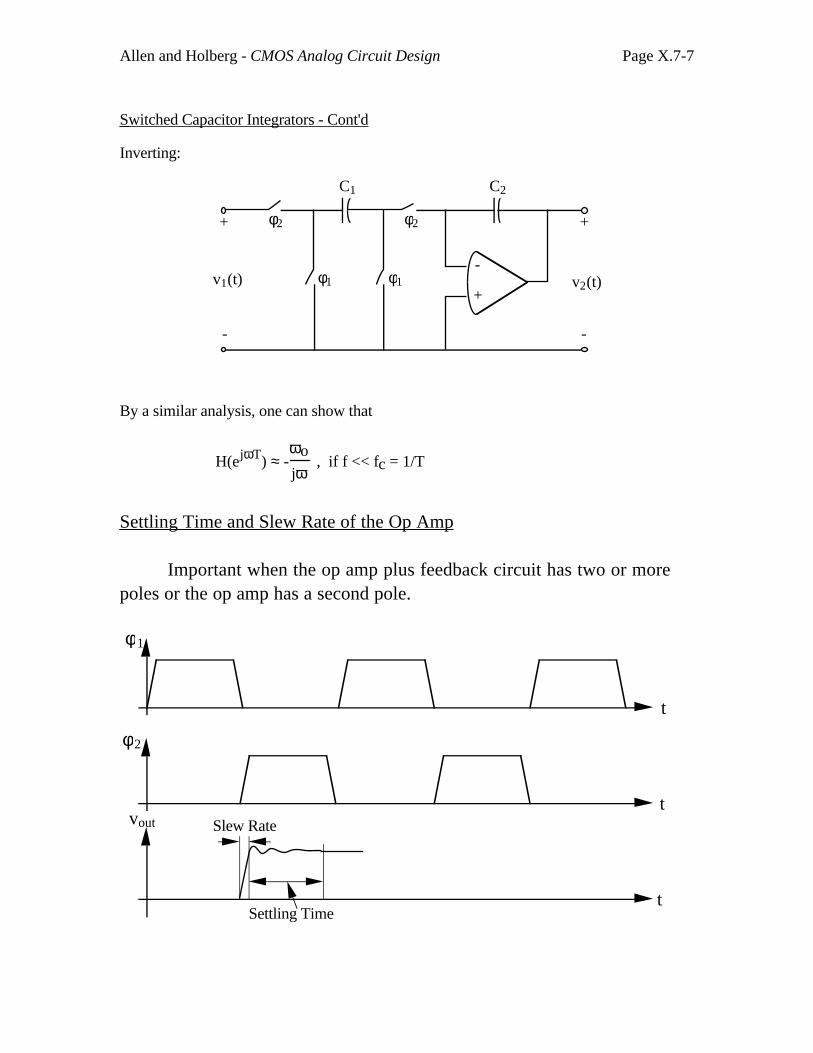
Allen and Holberg - CMOS Analog Circuit Design Page X.7-7
Switched Capacitor Integrators - Cont'd
Inverting:
-
-
+
-
v1(t) φ1
φ2+
φ1
φ2
C1 C2
+
v2(t)
By a similar analysis, one can show that
H(ejωT) ≈ -ωo
jω , if f << fc = 1/T
Settling Time and Slew Rate of the Op Amp
Important when the op amp plus feedback circuit has two or morepoles or the op amp has a second pole.
φ1
φ2
vout
t
t
t
Slew Rate
Settling Time
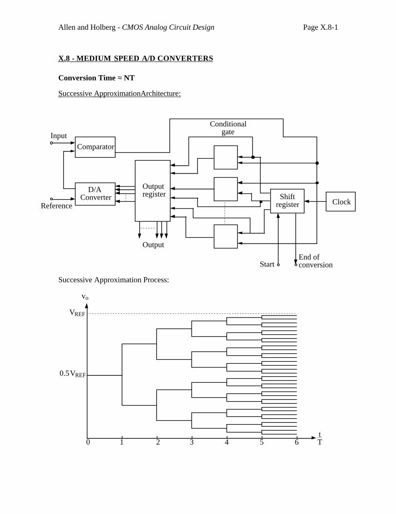
Allen and Holberg - CMOS Analog Circuit Design Page X.8-1
X.8 - MEDIUM SPEED A/D CONVERTERS
Conversion Time ≈ NT
Successive ApproximationArchitecture:
Successive Approximation Process:
VREF
0.5VREF
tT
vo
0 1 2 3 4 5 6
Outputregister
Comparator
D/AConverter
Clock
End of conversionStart
Shiftregister
Output
Input
Reference
Conditional gate
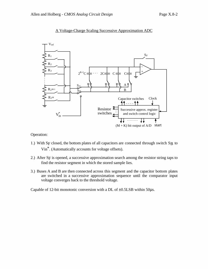
Allen and Holberg - CMOS Analog Circuit Design Page X.8-2
A Voltage-Charge Scaling Successive Approximation ADC
2C C C2K-1C+
_
Vref
R1
R2
R3
R2M-1
R2M
Successive approx. register and switch control logic
Capacitor switches Clock
(M + K) bit output of A/D
SF
SA
SB
Vin*
Resistorswitches
start
A
B
Operation:
1.) With SF closed, the bottom plates of all capacitors are connected through switch SB to
Vin*. (Automatically accounts for voltage offsets).
2.) After SF is opened, a successive approximation search among the resistor string taps tofind the resistor segment in which the stored sample lies.
3.) Buses A and B are then connected across this segment and the capacitor bottom platesare switched in a successive approximation sequence until the comparator inputvoltage converges back to the threshold voltage.
Capable of 12-bit monotonic conversion with a DL of ±0.5LSB within 50µs.
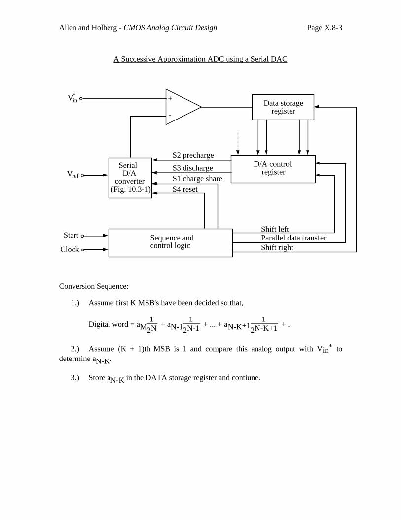
Allen and Holberg - CMOS Analog Circuit Design Page X.8-3
A Successive Approximation ADC using a Serial DAC
+
-
Data storage register
D/A control register
S2 precharge
S3 discharge Serial D/A converter(Fig. 10.3-1)
Sequence andcontrol logic
S1 charge shareS4 reset
Shift leftParallel data transferShift right
Start
Clock
Vref
Vin*
Conversion Sequence:
1.) Assume first K MSB's have been decided so that,
Digital word = aM1
2N + aN-11
2N-1 + ... + aN-K+11
2N-K+1 + .
2.) Assume (K + 1)th MSB is 1 and compare this analog output with Vin* todetermine aN-K.
3.) Store aN-K in the DATA storage register and contiune.
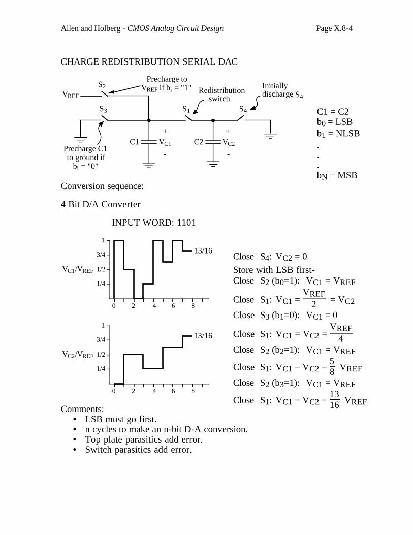
Allen and Holberg - CMOS Analog Circuit Design Page X.8-4
CHARGE REDISTRIBUTION SERIAL DAC
C1 C2+
-
VC1
+
-
VC2
S3 S1 S4
Precharge C1 to ground if
bi = "0"
Precharge toVREF if bi = "1"
VREF
S2Redistribution switch
Initiallydischarge S4
Conversion sequence:
4 Bit D/A Converter
INPUT WORD: 1101
0 2 4 86
1/4
1/2
3/4
1
VC1/VREF
13/16
0 2 4 86
1/4
1/2
3/4
1
VC2/VREF
13/16
Comments:• LSB must go first.• n cycles to make an n-bit D-A conversion.• Top plate parasitics add error.• Switch parasitics add error.
C1 = C2b0 = LSBb1 = NLSB...bN = MSB
Close S4: VC2 = 0
Store with LSB first-Close S2 (b0=1): VC1 = VREF
Close S1: VC1 = VREF
2 = VC2
Close S3 (b1=0): VC1 = 0
Close S1: VC1 = VC2 = VREF
4
Close S2 (b2=1): VC1 = VREF
Close S1: VC1 = VC2 = 58 VREF
Close S2 (b3=1): VC1 = VREF
Close S1: VC1 = VC2 = 1316 VREF
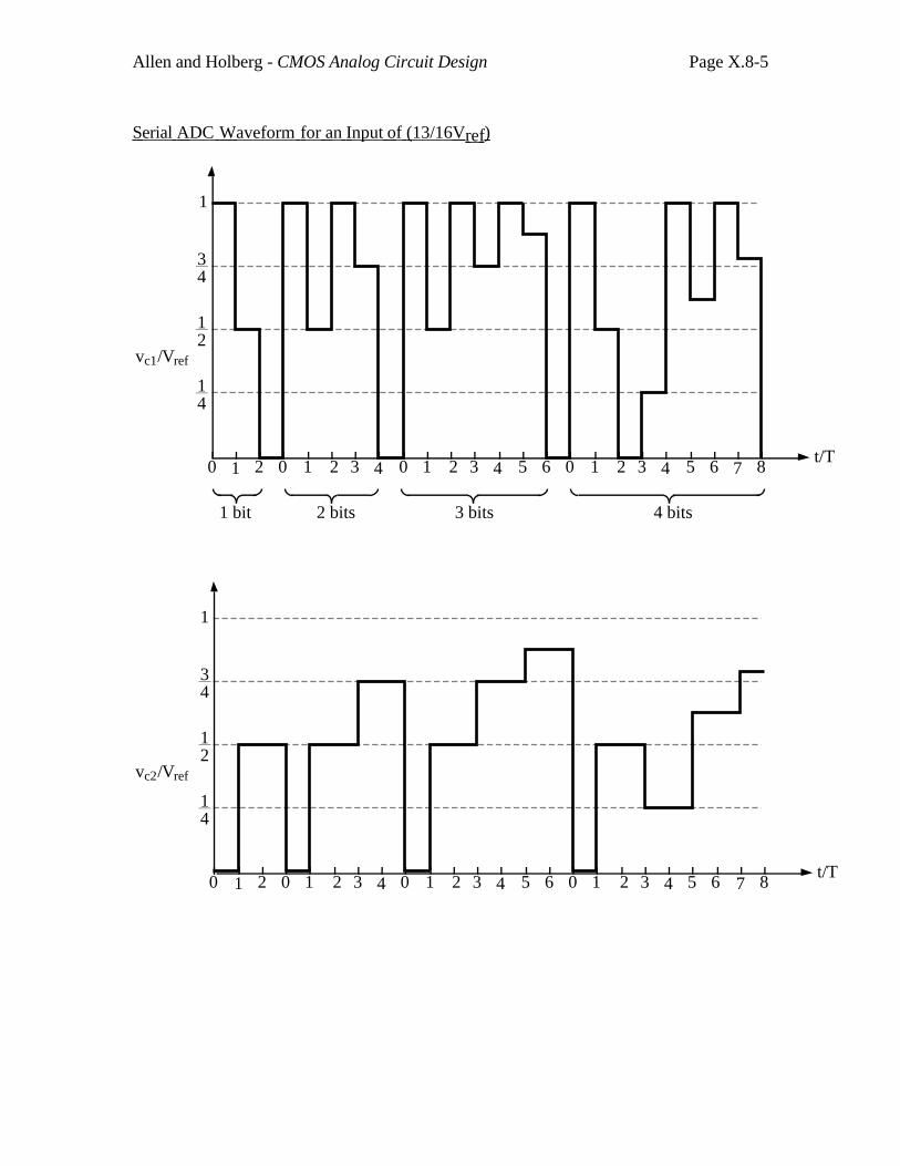
Allen and Holberg - CMOS Analog Circuit Design Page X.8-5
Serial ADC Waveform for an Input of (13/16V ref )
vc1/Vref
14
12
34
1
0 1 2 0 1 2 3 4 0 1 2 3 4 5 6 0 1 2 3 4 5 6 7 8t/T
4 bits3 bits2 bits1 bit
vc2/Vref
14
12
34
1
0 1 2 0 1 2 3 4 0 1 2 3 4 5 6 0 1 2 3 4 5 6 7 8t/T
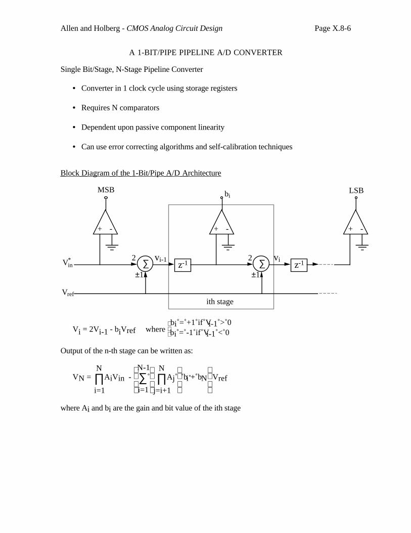
Allen and Holberg - CMOS Analog Circuit Design Page X.8-6
A 1-BIT/PIPE PIPELINE A/D CONVERTER
Single Bit/Stage, N-Stage Pipeline Converter
• Converter in 1 clock cycle using storage registers
• Requires N comparators
• Dependent upon passive component linearity
• Can use error correcting algorithms and self-calibration techniques
Block Diagram of the 1-Bit/Pipe A/D Architecture
+ -
z-1∑2
±1
+ -
z-1∑2
±1
+ -
vivi-1
MSB biLSB
ith stage
Vin*
Vref
Vi = 2Vi-1 - biVref where bi = +1 if Vi-1 > 0bi = -1 if Vi-1 < 0
Output of the n-th stage can be written as:
VN = ∏i=1
NAiVin -
∑i=1
N-1
∏j=i+1
NAj bi + bN Vref
where Ai and bi are the gain and bit value of the ith stage
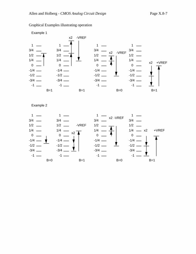
Allen and Holberg - CMOS Analog Circuit Design Page X.8-7
Graphical Examples illustrating operation
13/4
1/21/4
0
-1/4-1/2
-3/4-1
13/4
1/21/4
0
-1/4-1/2
-3/4-1
B=1 B=1
13/4
1/21/4
0
-1/4-1/2
-3/4-1
B=0
13/4
1/21/4
0
-1/4-1/2
-3/4-1
B=1
x2 -VREF
x2 -VREF
x2 +VREF
1
3/41/2
1/40
-1/4
-1/2-3/4
-1
1
3/41/2
1/40
-1/4
-1/2-3/4
-1B=0 B=1
1
3/41/2
1/40
-1/4
-1/2-3/4
-1B=0
1
3/41/2
1/40
-1/4
-1/2-3/4
-1
x2
-VREF
x2 -VREF
x2 +VREF
B=1
Example 1
Example 2
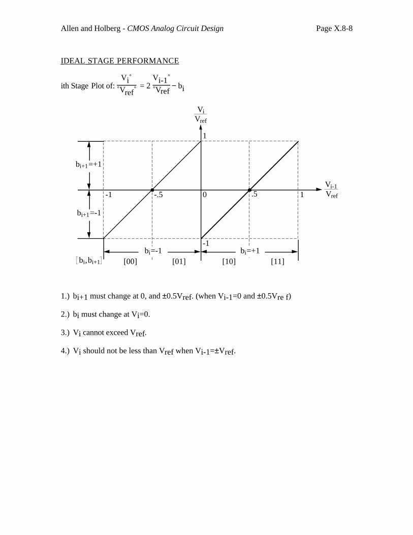
Allen and Holberg - CMOS Analog Circuit Design Page X.8-8
IDEAL STAGE PERFORMANCE
ith Stage Plot of: Vi
Vref = 2
Vi-1
Vref − bi
0 .5 1
1
-1
-.5-1
ViVref
bi+1=+1
bi+1=-1
bi=-1[00] [01]
bi=+1[10] [11]bi,bi+1
Vi-1Vref
1.) bi+1 must change at 0, and ±0.5Vref. (when Vi-1=0 and ±0.5Vre f)
2.) bi must change at Vi=0.
3.) Vi cannot exceed Vref.
4.) Vi should not be less than Vref when Vi-1=±Vref.
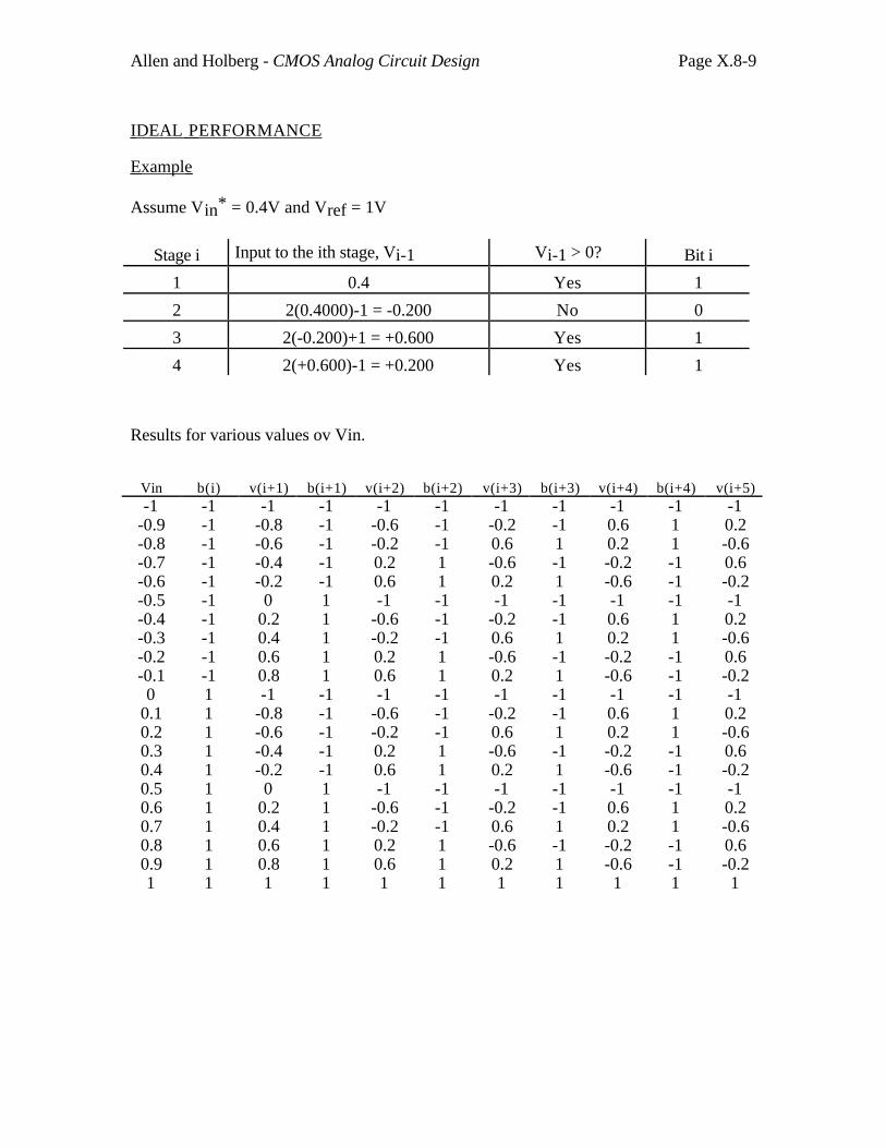
Allen and Holberg - CMOS Analog Circuit Design Page X.8-9
IDEAL PERFORMANCE
Example
Assume Vin* = 0.4V and Vref = 1V
Stage i Input to the ith stage, Vi-1 Vi-1 > 0? Bit i
1 0.4 Yes 1
2 2(0.4000)-1 = -0.200 No 0
3 2(-0.200)+1 = +0.600 Yes 1
4 2(+0.600)-1 = +0.200 Yes 1
Results for various values ov Vin.
Vin b(i) v(i+1) b(i+1) v(i+2) b(i+2) v(i+3) b(i+3) v(i+4) b(i+4) v(i+5)-1 -1 -1 -1 -1 -1 -1 -1 -1 -1 -1
-0.9 -1 -0.8 -1 -0.6 -1 -0.2 -1 0.6 1 0.2-0.8 -1 -0.6 -1 -0.2 -1 0.6 1 0.2 1 -0.6-0.7 -1 -0.4 -1 0.2 1 -0.6 -1 -0.2 -1 0.6-0.6 -1 -0.2 -1 0.6 1 0.2 1 -0.6 -1 -0.2-0.5 -1 0 1 -1 -1 -1 -1 -1 -1 -1-0.4 -1 0.2 1 -0.6 -1 -0.2 -1 0.6 1 0.2-0.3 -1 0.4 1 -0.2 -1 0.6 1 0.2 1 -0.6-0.2 -1 0.6 1 0.2 1 -0.6 -1 -0.2 -1 0.6-0.1 -1 0.8 1 0.6 1 0.2 1 -0.6 -1 -0.20 1 -1 -1 -1 -1 -1 -1 -1 -1 -1
0.1 1 -0.8 -1 -0.6 -1 -0.2 -1 0.6 1 0.20.2 1 -0.6 -1 -0.2 -1 0.6 1 0.2 1 -0.60.3 1 -0.4 -1 0.2 1 -0.6 -1 -0.2 -1 0.60.4 1 -0.2 -1 0.6 1 0.2 1 -0.6 -1 -0.20.5 1 0 1 -1 -1 -1 -1 -1 -1 -10.6 1 0.2 1 -0.6 -1 -0.2 -1 0.6 1 0.20.7 1 0.4 1 -0.2 -1 0.6 1 0.2 1 -0.60.8 1 0.6 1 0.2 1 -0.6 -1 -0.2 -1 0.60.9 1 0.8 1 0.6 1 0.2 1 -0.6 -1 -0.21 1 1 1 1 1 1 1 1 1 1
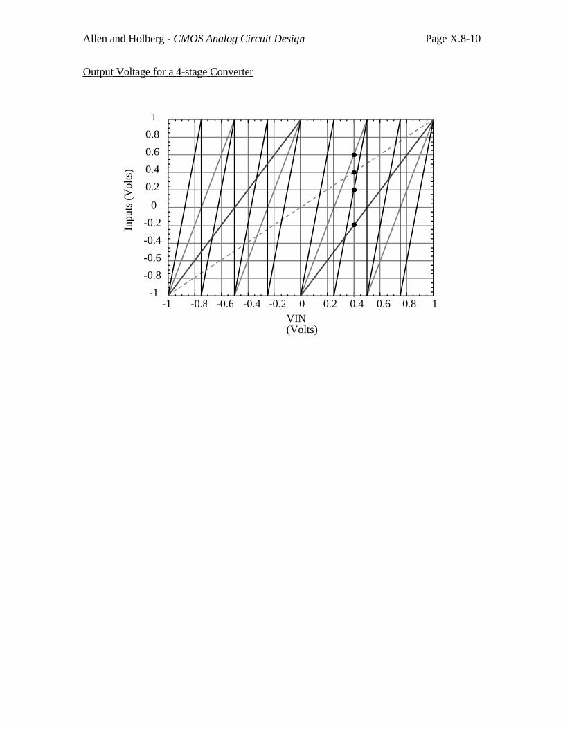
Allen and Holberg - CMOS Analog Circuit Design Page X.8-10
Output Voltage for a 4-stage Converter
-1
-0.8
-0.6
-0.4
-0.2
0
0.2
Inpu
ts (
Vol
ts) 0.4
0.6
0.8
1
-1 -0.8 -0.6VIN (Volts)
-0.4 -0.2 0 0.2 0.4 0.6 0.8 1
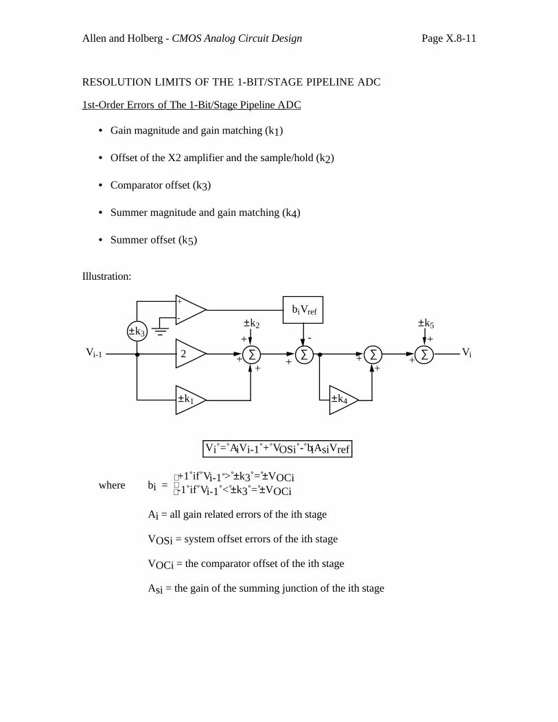
Allen and Holberg - CMOS Analog Circuit Design Page X.8-11
RESOLUTION LIMITS OF THE 1-BIT/STAGE PIPELINE ADC
1st-Order Errors of The 1-Bit/Stage Pipeline ADC
• Gain magnitude and gain matching (k1)
• Offset of the X2 amplifier and the sample/hold (k2)
• Comparator offset (k3)
• Summer magnitude and gain matching (k4)
• Summer offset (k5)
Illustration:
∑
+
-biVref
∑ ∑ ∑
±k3 -
+
±k2
+
++
2
±k1
++
±k4
±k5
+
+ViVi-1
Vi = AiVi-1 + VOSi - biAsiVref
where bi = +1 if Vi-1 > ±k3 = ±VOCi-1 if Vi-1 < ±k3 = ±VOCi
Ai = all gain related errors of the ith stage
VOSi = system offset errors of the ith stage
VOCi = the comparator offset of the ith stage
Asi = the gain of the summing junction of the ith stage
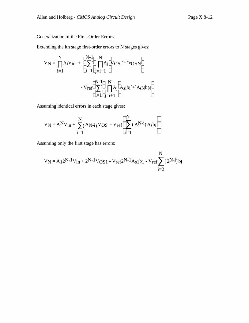
Allen and Holberg - CMOS Analog Circuit Design Page X.8-12
Generalization of the First-Order Errors
Extending the ith stage first-order errors to N stages gives:
VN = ∏i=1
NAiVin +
∑i=1
N-1
∏j=i+1
NAj VOSi + VOSN
- Vref
∑i=1
N-1
∏j=i+1
NAj Asibi + AsNbN
Assuming identical errors in each stage gives:
VN = ANVin + ∑i=1
N( )AN-i VOS - Vref
∑
i=1
N
( )AN-i Asbi
Assuming only the first stage has errors:
VN = A12N-1Vin + 2N-1VOS1 - Vref2N-1As1b1 - Vref∑i=2
N
( )2N-i bi
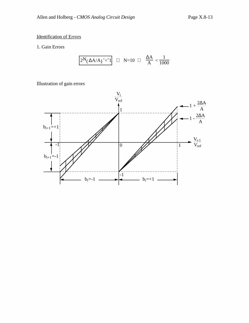
Allen and Holberg - CMOS Analog Circuit Design Page X.8-13
Identification of Errors
1. Gain Errors
2N( )∆A/A < 1 ⇒ N=10 ⇒ ∆AA <
11000
Illustration of gain errors
0 1
1
-1
-1
ViVref
bi+1=+1
bi+1=-1
bi=-1 bi=+1
Vi-1Vref
1 + 2∆A
A
1 - 2∆A
A
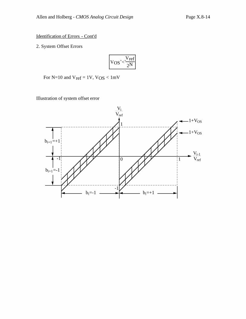
Allen and Holberg - CMOS Analog Circuit Design Page X.8-14
Identification of Errors - Cont'd
2. System Offset Errors
VOS < Vref
2N
For N=10 and Vref = 1V, VOS < 1mV
Illustration of system offset error
0 1
1
-1
-1
ViVref
bi+1=+1
bi+1=-1
bi=-1 bi=+1
Vi-1Vref
1+VOS
1+VOS
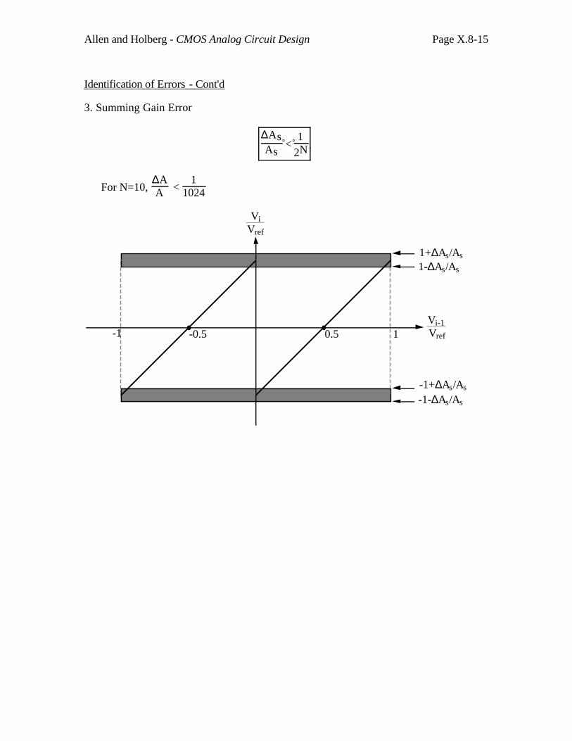
Allen and Holberg - CMOS Analog Circuit Design Page X.8-15
Identification of Errors - Cont'd
3. Summing Gain Error
∆AsAs
< 1
2N
For N=10, ∆AA <
11024
1
ViVref
Vi-1Vref0.5-0.5-1
1+∆As/As
1-∆As/As
-1-∆As/As
-1+∆As/As
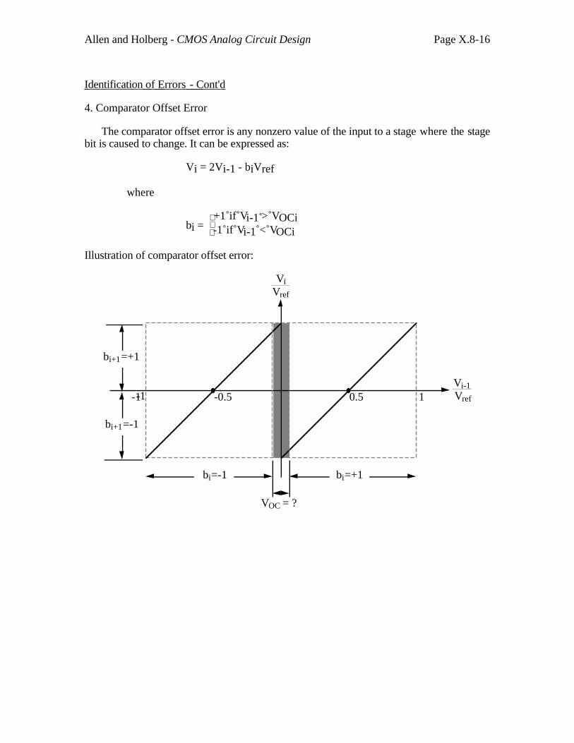
Allen and Holberg - CMOS Analog Circuit Design Page X.8-16
Identification of Errors - Cont'd
4. Comparator Offset Error
The comparator offset error is any nonzero value of the input to a stage where the stagebit is caused to change. It can be expressed as:
Vi = 2Vi-1 - biVref
where
bi = +1 if Vi-1 > VOCi-1 if Vi-1 < VOCi
Illustration of comparator offset error:
1
ViVref
Vi-1Vref0.5-0.5-1-1
bi+1=+1
bi+1=-1
bi=-1 bi=+1
VOC = ?

Allen and Holberg - CMOS Analog Circuit Design Page X.8-17
SUMMARY
1.) The 1-bit/pipe, pipeline converter which uses standard components including a sampleand hold, an amplifier, and a comparator would be capable of realizing at most an 8 or 9 bitconverter.
2.) The accuracy of the gains and offset of the first stage of an N-Bit converter must bewithin 0.5LSB.
3.) The accuracy of the gains and offset of a stage diminishes with the remaining numberof stages to the output of the converter.
4.) Error correction and self-calibrating techniques are necessary in order to realize thepotential resolution capability of the 1-bit/'stage pipeline ADC.
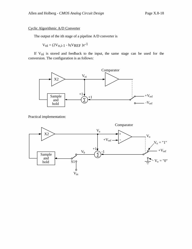
Allen and Holberg - CMOS Analog Circuit Design Page X.8-18
Cyclic Algorithmic A/D Converter
The output of the ith stage of a pipeline A/D converter is
Voi = (2Vo,i-1 - biVREF )z-1
If Voi is stored and feedback to the input, the same stage can be used for theconversion. The configuration is as follows:
X2
∑Sample and hold
+1 +Vref
-Vref
+1
Voi
Comparator
Practical implementation:
∑
X2
Sample and hold
+1 +Vref-1
Comparator
+Vref
+
-
Vb
S1
Va
Vo
Vo = "1"
Vo = "0"
Vin
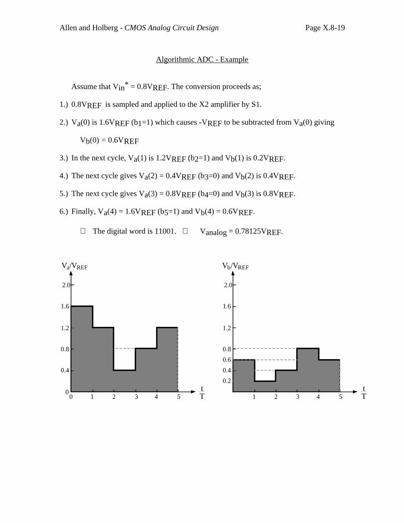
Allen and Holberg - CMOS Analog Circuit Design Page X.8-19
Algorithmic ADC - Example
Assume that Vin* = 0.8VREF. The conversion proceeds as;
1.) 0.8VREF is sampled and applied to the X2 amplifier by S1.
2.) Va(0) is 1.6VREF (b1=1) which causes -VREF to be subtracted from Va(0) giving
Vb(0) = 0.6VREF
3.) In the next cycle, Va(1) is 1.2VREF (b2=1) and Vb(1) is 0.2VREF.
4.) The next cycle gives Va(2) = 0.4VREF (b3=0) and Vb(2) is 0.4VREF.
5.) The next cycle gives Va(3) = 0.8VREF (b4=0) and Vb(3) is 0.8VREF.
6.) Finally, Va(4) = 1.6VREF (b5=1) and Vb(4) = 0.6VREF.
∴ The digital word is 11001. ⇒ Vanalog = 0.78125VREF.
00
1 2 3 4 5
0.4
0.8
1.2
1.6
2.0
1 2 3 4 5
0.4
0.8
1.2
1.6
2.0
tT
tT
Va/VREF Vb/VREF
0.6
0.2
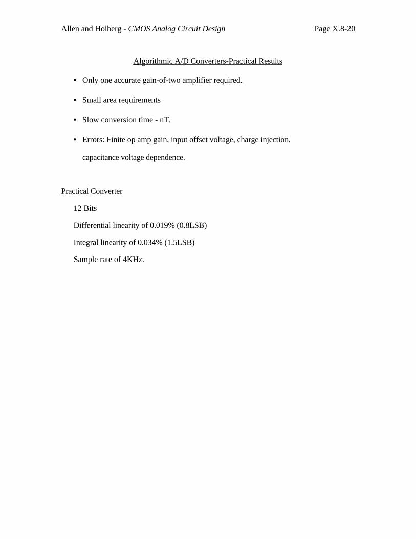
Allen and Holberg - CMOS Analog Circuit Design Page X.8-20
Algorithmic A/D Converters-Practical Results
• Only one accurate gain-of-two amplifier required.
• Small area requirements
• Slow conversion time - nT.
• Errors: Finite op amp gain, input offset voltage, charge injection,
capacitance voltage dependence.
Practical Converter
12 Bits
Differential linearity of 0.019% (0.8LSB)
Integral linearity of 0.034% (1.5LSB)
Sample rate of 4KHz.
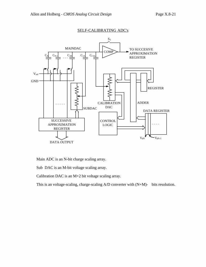
Allen and Holberg - CMOS Analog Circuit Design Page X.8-21
SELF-CALIBRATING ADC's
CCALC1AC1BCN-1CN
Vref
GND
SUCCESSIVEAPPROXIMATION REGISTER
DATA OUTPUT
SUBDAC
COMP
CALIBRATION DAC
CONTROL LOGIC
DATA REGISTER
ADDER
REGISTER
TO SUCCESIVEAPPROXIMATIONREGISTER
VεN VεN-1
MAINDAC
S1
Main ADC is an N-bit charge scaling array.
Sub DAC is an M-bit voltage scaling array.
Calibration DAC is an M+2 bit voltage scaling array.
This is an voltage-scaling, charge-scaling A/D converter with (N+M)- bits resolution.
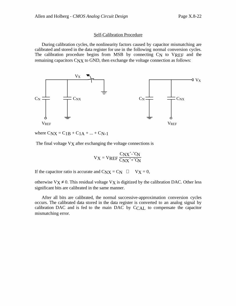
Allen and Holberg - CMOS Analog Circuit Design Page X.8-22
Self-Calibration Procedure
During calibration cycles, the nonlinearity factors caused by capacitor mismatching arecalibrated and stored in the data register for use in the following normal conversion cycles.The calibration procedure begins from MSB by connecting CN to VREF and theremaining capacitors CNX to GND, then exchange the voltage connection as follows:
CN CNX CNXCN
VX
VREF VREF
VX
where CNX = C1B + C1A + ... + CN-1
The final voltage VX after exchanging the voltage connections is
VX = VREF CNX - CNCNX + CN
If the capacitor ratio is accurate and CNX = CN ⇒ VX = 0,
otherwise VX ≠ 0. This residual voltage VX is digitized by the calibration DAC. Other lesssignificant bits are calibrated in the same manner.
After all bits are calibrated, the normal successive-approximation conversion cyclesoccurs. The calibrated data stored in the data register is converted to an analog signal bycalibration DAC and is fed to the main DAC by CCAL to compensate the capacitormismatching error.
Allen and Holberg - CMOS Analog Circuit Design Page X.8-23
Self-Calibrating ADC Performance
Supply voltage ± 5V
Resolution of 16 bits
Linearity of 16 bits
Offset less than 0.25 LSB
Conversion time for 0.5 LSB linearity:
12 µs for 12 Bits
80 µs for 16 Bits.
RMS noise of 40 µV.
Power dissipation of 20 mW (excludes logic)
Area of 7.5 mm (excludes logic).

Allen and Holberg - CMOS Analog Circuit Design Page X.9-1
X.9 - HIGH SPEED ADC's
Conversion Time ≈ T (T = clock period)
• Flash or parallel
• Time interleaving
• Pipeline - Multiple Bits
• Pipeline - Single Bit
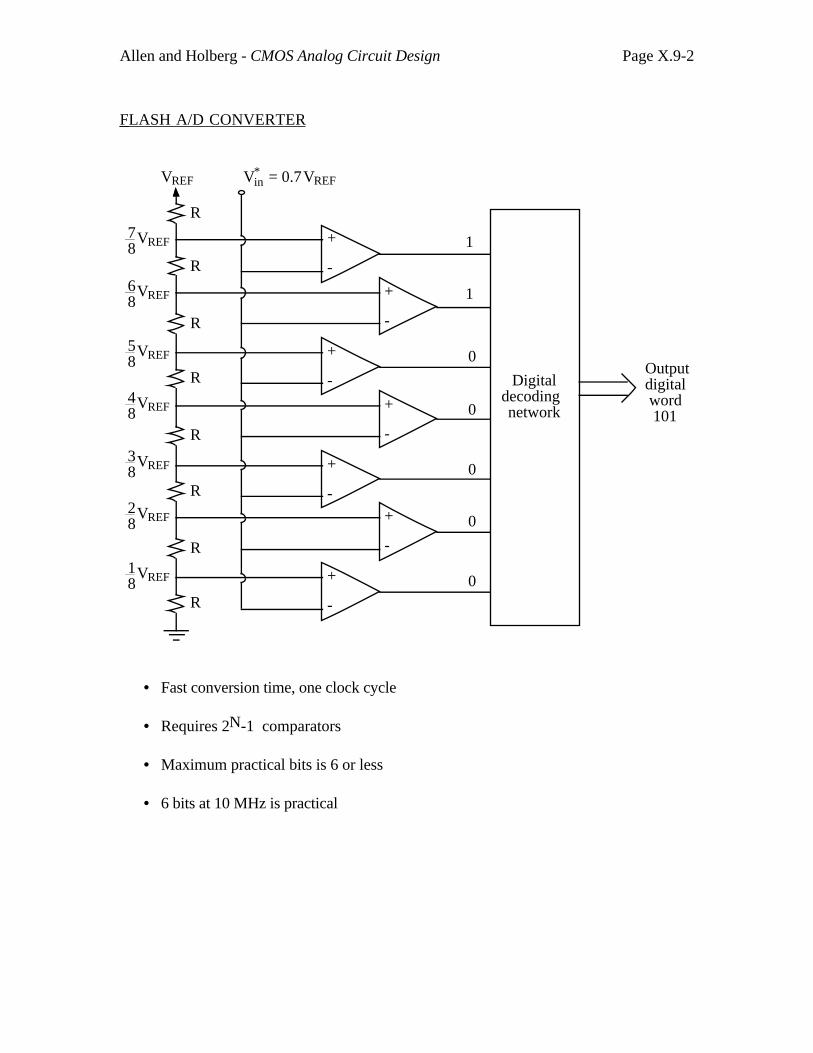
Allen and Holberg - CMOS Analog Circuit Design Page X.9-2
FLASH A/D CONVERTER
+
-
+
-
+
-
+
-
+
-
+
-
+
-
Digitaldecoding network
1
1
0
0
0
0
0
Outputdigital word 101
R
R
R
R
R
R
R
R
78
VREF
68
VREF
58
VREF
48
VREF
38
VREF
28
VREF
18
VREF
VREF Vin* = 0.7VREF
• Fast conversion time, one clock cycle
• Requires 2N-1 comparators
• Maximum practical bits is 6 or less
• 6 bits at 10 MHz is practical
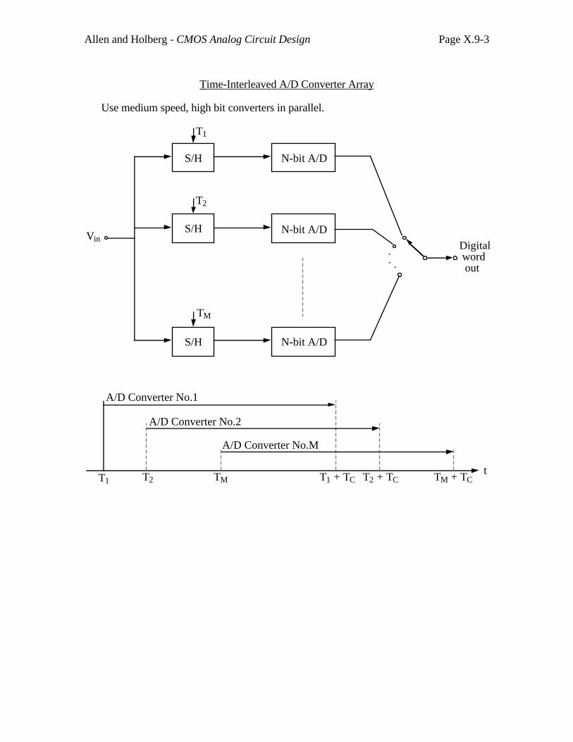
Allen and Holberg - CMOS Analog Circuit Design Page X.9-3
Time-Interleaved A/D Converter Array
Use medium speed, high bit converters in parallel.
N-bit A/D
N-bit A/DS/H
S/H
N-bit A/DS/H
T1
T2
TM
VinDigital word out
.
. .
tT1 T2 TM T1 + TC T2 + TC TM + TC
A/D Converter No.1
A/D Converter No.2
A/D Converter No.M
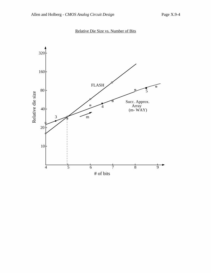
Allen and Holberg - CMOS Analog Circuit Design Page X.9-4
Relative Die Size vs. Number of Bits
10
20
40
80
160
320
4 5 6 7 8 9
# of bits
Rel
ativ
e di
e si
ze
3
4
5
m
Succ. Approx. Array (m- WAY)
FLASH
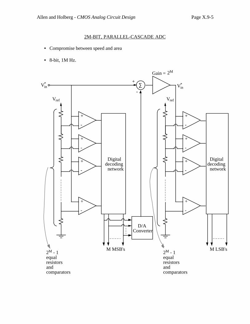
Allen and Holberg - CMOS Analog Circuit Design Page X.9-5
2M-BIT, PARALLEL-CASCADE ADC
• Compromise between speed and area
• 8-bit, 1M Hz.
Digitaldecoding network
2M - 1equalresistorsand comparators
Vref
2M - 1equalresistorsand comparators
Digitaldecoding network
+
-
+
-
+
-
+
-
Vref
D/AConverter
∑Vin*
Gain = 2M
Vin*
M LSB'sM MSB's
+
-
+
-
+
-
+
-
+
-
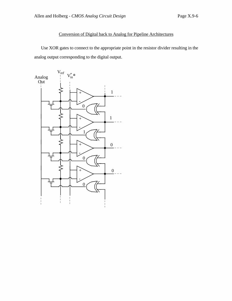
Allen and Holberg - CMOS Analog Circuit Design Page X.9-6
Conversion of Digital back to Analog for Pipeline Architectures
Use XOR gates to connect to the appropriate point in the resistor divider resulting in the
analog output corresponding to the digital output.
VrefVin
*
+
-
+
-
+
-
+
-
1
1
0
0
0
1
0
0
AnalogOut
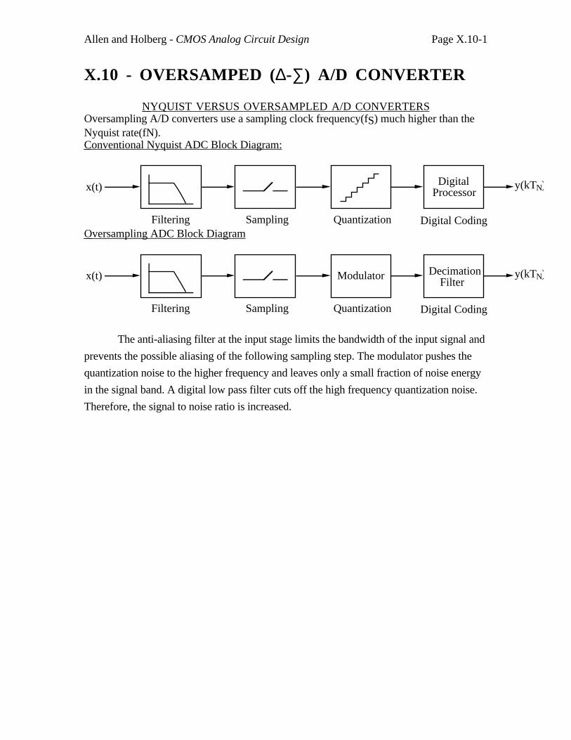
Allen and Holberg - CMOS Analog Circuit Design Page X.10-1
X.10 - OVERSAMPED (∆-∑) A/D CONVERTER
NYQUIST VERSUS OVERSAMPLED A/D CONVERTERSOversampling A/D converters use a sampling clock frequency(fS) much higher than theNyquist rate(fN). Conventional Nyquist ADC Block Diagram:
x(t)
Filtering Sampling Quantization
DigitalProcessor
Digital Coding
y(kTN)
Oversampling ADC Block Diagram
x(t)
Filtering Sampling Quantization Digital Coding
y(kTN)Modulator Decimation Filter
The anti-aliasing filter at the input stage limits the bandwidth of the input signal and
prevents the possible aliasing of the following sampling step. The modulator pushes the
quantization noise to the higher frequency and leaves only a small fraction of noise energy
in the signal band. A digital low pass filter cuts off the high frequency quantization noise.
Therefore, the signal to noise ratio is increased.
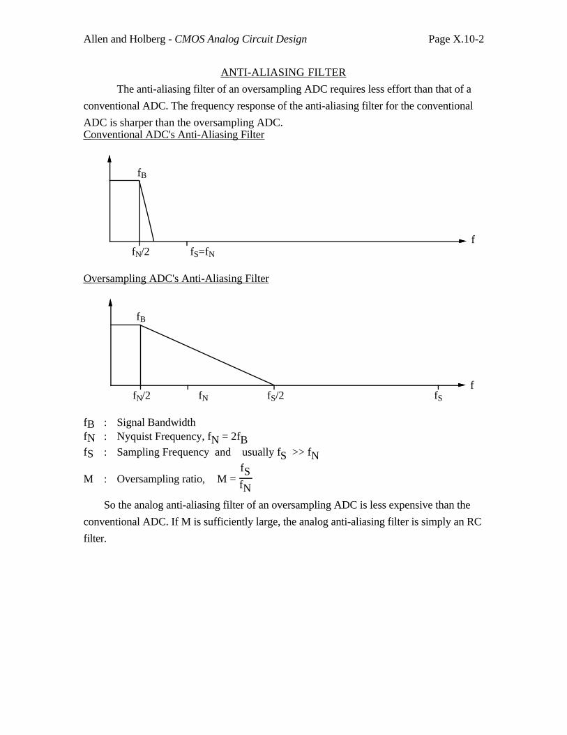
Allen and Holberg - CMOS Analog Circuit Design Page X.10-2
ANTI-ALIASING FILTER
The anti-aliasing filter of an oversampling ADC requires less effort than that of a
conventional ADC. The frequency response of the anti-aliasing filter for the conventional
ADC is sharper than the oversampling ADC. Conventional ADC's Anti-Aliasing Filter
ffN/2 fS=fN
fB
Oversampling ADC's Anti-Aliasing Filter
ffN/2 fN fS/2 fS
fB
fB : Signal BandwidthfN : Nyquist Frequency, fN = 2fBfS : Sampling Frequency and usually fS >> fN
M : Oversampling ratio, M = fSfN
So the analog anti-aliasing filter of an oversampling ADC is less expensive than the
conventional ADC. If M is sufficiently large, the analog anti-aliasing filter is simply an RC
filter.
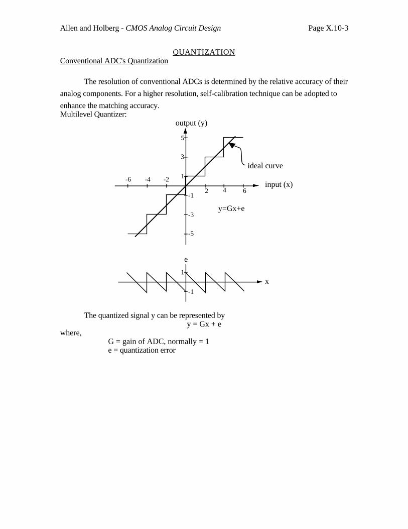
Allen and Holberg - CMOS Analog Circuit Design Page X.10-3
QUANTIZATION Conventional ADC's Quantization
The resolution of conventional ADCs is determined by the relative accuracy of their
analog components. For a higher resolution, self-calibration technique can be adopted to
enhance the matching accuracy.Multilevel Quantizer:
input (x)
output (y)
2 4 6
-2-4-6 1
3
5
-1
-3
-5
y=Gx+e
e
x1
-1
ideal curve
The quantized signal y can be represented byy = Gx + e
where,G = gain of ADC, normally = 1e = quantization error
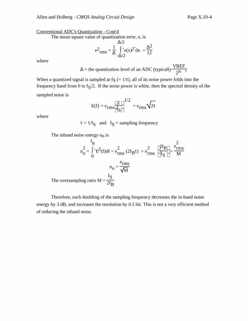
Allen and Holberg - CMOS Analog Circuit Design Page X.10-4
Conventional ADC's Quantization - Cont'dThe mean square value of quantization error, e, is
e2rms =
1∆ ⌡⌠
-∆/2
∆/2
e(x)2 dx = ∆2
12
where
∆ = the quantization level of an ADC (typically VREF
2N )
When a quantized signal is sampled at fS (= 1/τ), all of its noise power folds into thefrequency band from 0 to fS/2. If the noise power is white, then the spectral density of the
sampled noise is
E(f) = erms
2
fS 1/2
= erms 2τ
whereτ = 1/fS and fS = sampling frequency
The inband noise energy no is
n2o = ⌡⌠
0
fB
E2(f)df = e2rms (2fBτ) = e
2rms
2fB
fS =
e2rmsM
no = erms
M
The oversampling ratio M = fS2fB
Therefore, each doubling of the sampling frequency decreases the in-band noise
energy by 3 dB, and increases the resolution by 0.5 bit. This is not a very efficient method
of reducing the inband noise.
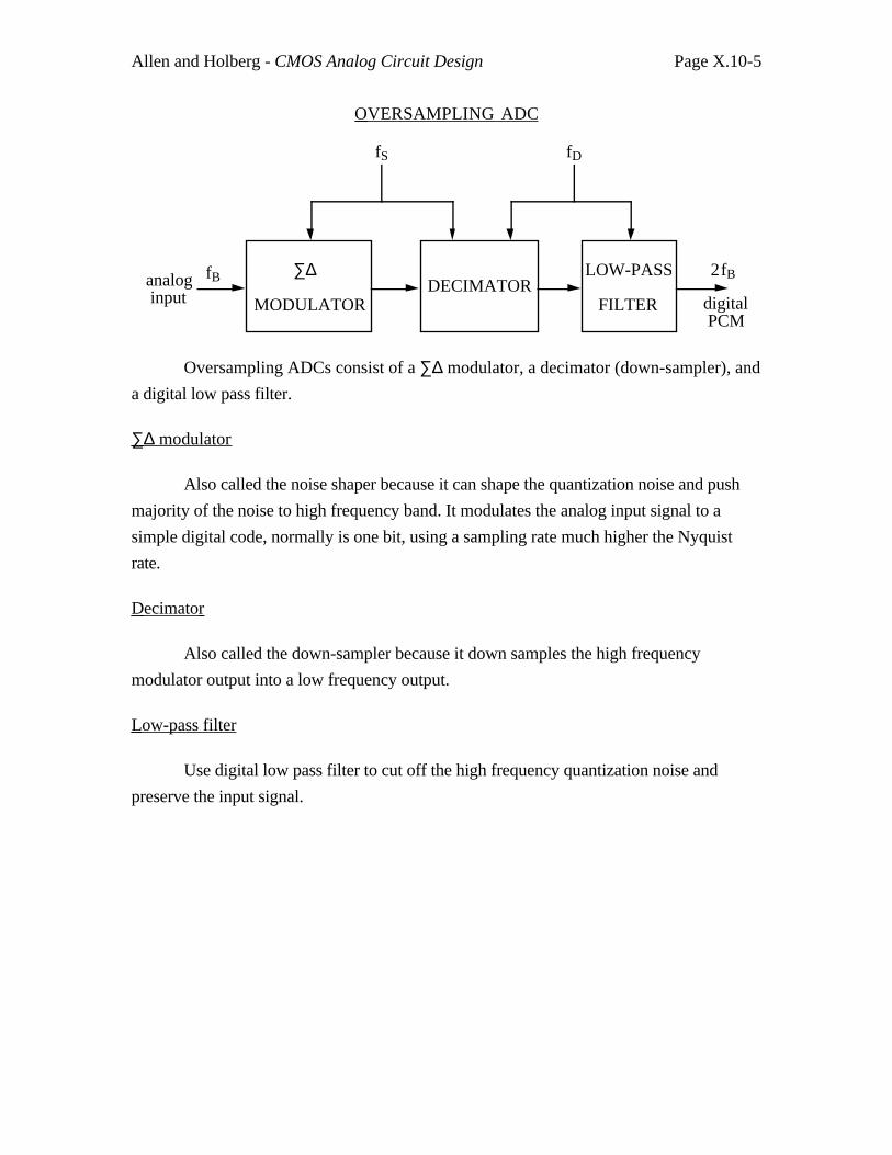
Allen and Holberg - CMOS Analog Circuit Design Page X.10-5
OVERSAMPLING ADC
∑∆ MODULATOR
DECIMATORLOW-PASS
FILTER
analog input
fDfS
2fB
digital PCM
fB
Oversampling ADCs consist of a ∑∆ modulator, a decimator (down-sampler), and
a digital low pass filter.
∑∆ modulator
Also called the noise shaper because it can shape the quantization noise and push
majority of the noise to high frequency band. It modulates the analog input signal to a
simple digital code, normally is one bit, using a sampling rate much higher the Nyquist
rate.
Decimator
Also called the down-sampler because it down samples the high frequency
modulator output into a low frequency output.
Low-pass filter
Use digital low pass filter to cut off the high frequency quantization noise and
preserve the input signal.
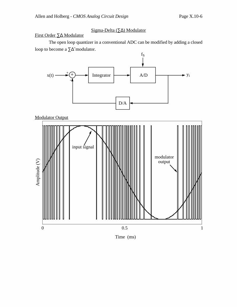
Allen and Holberg - CMOS Analog Circuit Design Page X.10-6
Sigma-Delta (∑∆) Modulator First Order ∑∆ Modulator
The open loop quantizer in a conventional ADC can be modified by adding a closed
loop to become a ∑∆ modulator.
Integrator A/D
D/A
++
-x(t)
fS
yi
Modulator Output
0 10.5
Time (ms)
input signal
modulator output
Am
plitu
de (
V)
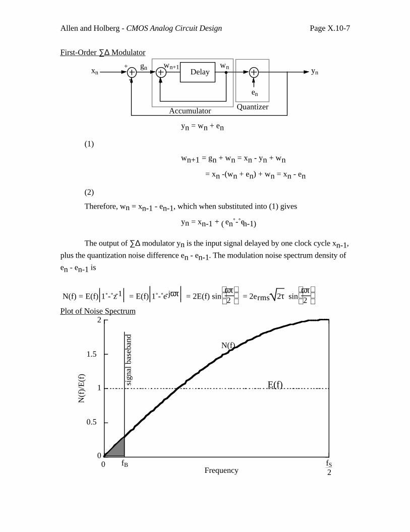
Allen and Holberg - CMOS Analog Circuit Design Page X.10-7
First-Order ∑∆ Modulator
Delay
QuantizerAccumulator
+
-xn
wngn yn
en
wn+1
yn = wn + en
(1)
wn+1 = gn + wn = xn - yn + wn
= xn -(wn + en) + wn = xn - en
(2)
Therefore, wn = xn-1 - en-1, which when substituted into (1) gives
yn = xn-1 + ( )en - en-1
The output of ∑∆ modulator yn is the input signal delayed by one clock cycle xn-1,
plus the quantization noise difference en - en-1. The modulation noise spectrum density of
en - en-1 is
N(f) = E(f) 1 - z-1 = E(f) 1 - e-jωτ = 2E(f) sin
ωτ
2 = 2erms 2τ sin
ωτ
2
Plot of Noise Spectrum
fS2
N(f
)/E
(f)
fB
sign
al b
aseb
and
0
0.5
1
1.5
2
0
E(f)
Frequency
N(f)
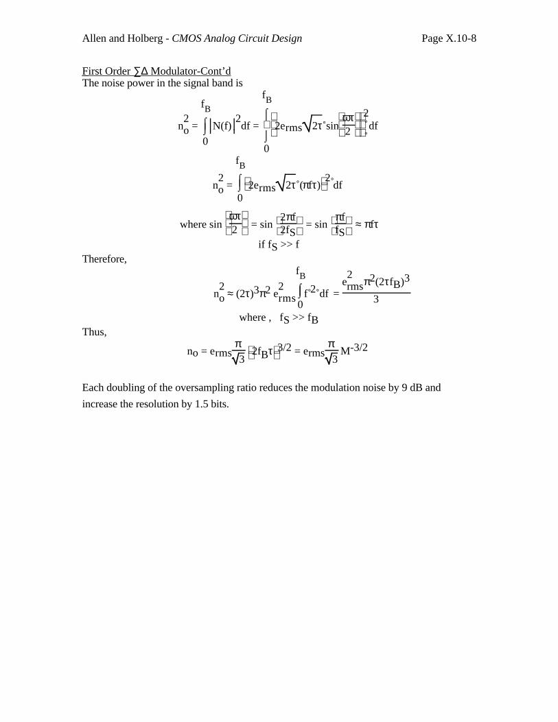
Allen and Holberg - CMOS Analog Circuit Design Page X.10-8
First Order ∑∆ Modulator-Cont’dThe noise power in the signal band is
n2o = ⌡⌠
0
fB
N(f)2df =
⌡⌠
0
fB
2erms 2τ sin
ωτ
2
2 df
n2o = ⌡⌠
0
fB
2erms 2τ (πfτ)2 df
where sin
ωτ
2 = sin
2πf
2fS = sin
πf
fS ≈ πfτ
if fS >> fTherefore,
n2o ≈ (2τ)3π2 e
2rms
⌡⌠0
fB
f 2 df = e2rmsπ2(2τfB)3
3
where , fS >> fBThus,
no = ermsπ3 2fBτ 3/2 = erms
π3 M-3/2
Each doubling of the oversampling ratio reduces the modulation noise by 9 dB and
increase the resolution by 1.5 bits.
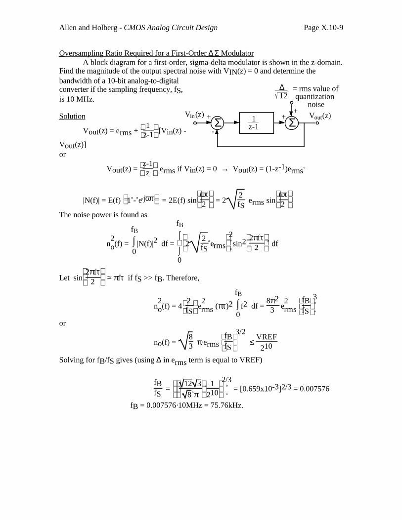
Allen and Holberg - CMOS Analog Circuit Design Page X.10-9
Oversampling Ratio Required for a First-Order ∆Σ ModulatorA block diagram for a first-order, sigma-delta modulator is shown in the z-domain.
Find the magnitude of the output spectral noise with VIN(z) = 0 and determine thebandwidth of a 10-bit analog-to-digitalconverter if the sampling frequency, fS,is 10 MHz.
Solution
Vout(z) = erms +
1
z-1 [Vin(z) -
Vout(z)]or
Vout(z) =
z-1
z erms if Vin(z) = 0 → Vout(z) = (1-z-1)erms
|N(f)| = E(f) 1 - e-jωτ = 2E(f) sin
ωτ
2 = 22fS
erms sin
ωτ
2
The noise power is found as
n2o(f) = ⌡⌠
0
fB
|N(f)|2 df = ⌡⌠
0
fB
22fS
erms
2 sin2
2πfτ
2 df
Let sin
2πfτ
2 ≈ πfτ if fS >> fB. Therefore,
n2o(f) = 4
2
fS e
2rms (πτ)2 ⌡⌠
0
fB
f2 df = 8π2
3 e2rms
fB
fS
3
or
no(f) = 83 π·erms
fB
fS
3/2 ≤
VREF
210
Solving for fB/fS gives (using ∆ in erms term is equal to VREF)
fBfS
=
12 3
8 π
1
210
2/3
= [0.659x10⁻³]2/3 = 0.007576
fB = 0.007576·10MHz = 75.76kHz.
Σ Σ
∆12
Vout(z)Vin(z) ++
+
-
= rms value ofquantization
noise
1z-1
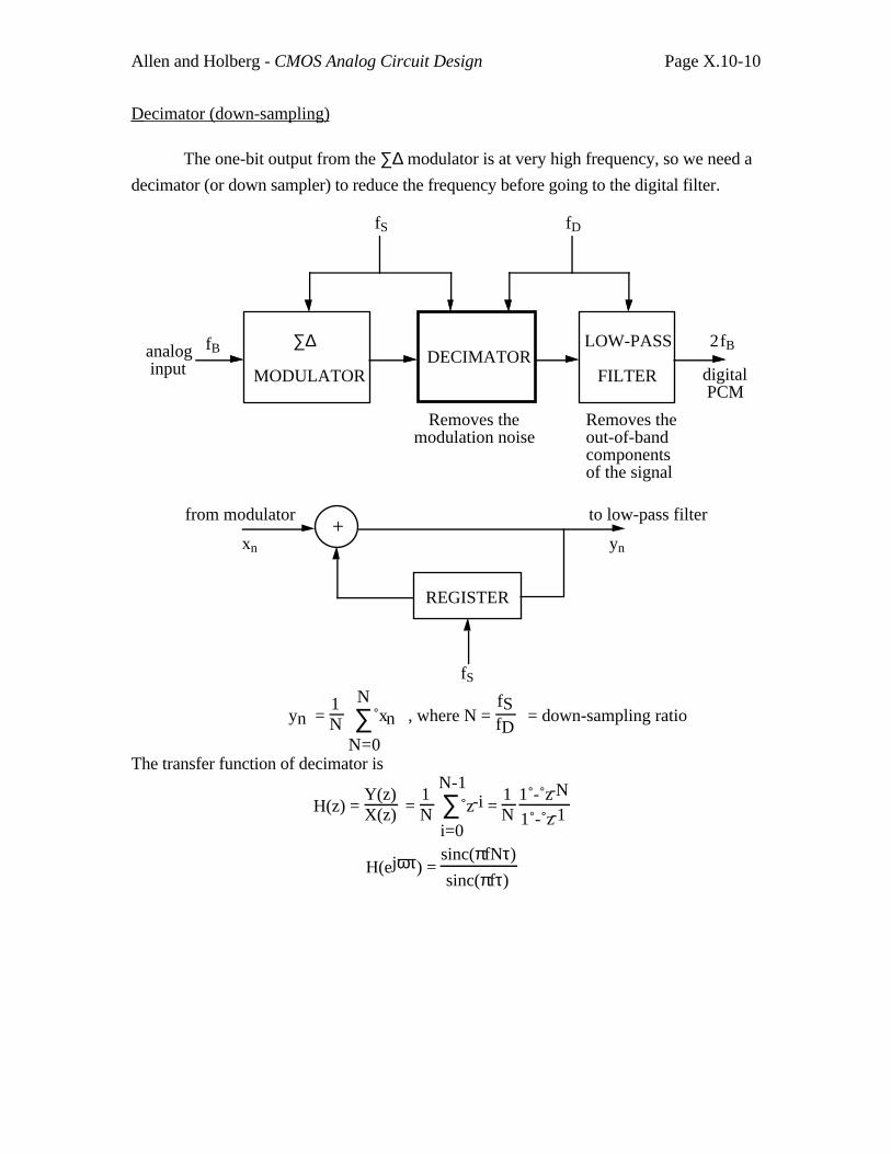
Allen and Holberg - CMOS Analog Circuit Design Page X.10-10
Decimator (down-sampling)
The one-bit output from the ∑∆ modulator is at very high frequency, so we need a
decimator (or down sampler) to reduce the frequency before going to the digital filter.
∑∆ MODULATOR
DECIMATORLOW-PASS
FILTER
analog input
fDfS
2fB
digital PCM
fB
Removes themodulation noise
Removes the out-of-band componentsof the signal
REGISTER
+
fS
from modulator to low-pass filter
xn yn
yn = 1N ∑
N=0
N xn , where N =
fSfD
= down-sampling ratio
The transfer function of decimator is
H(z) = Y(z)X(z) =
1N ∑
i=0
N-1 z-i =
1N
1 - z-N
1 - z-1
H(ejωτ) = sinc(πfNτ)
sinc(πfτ)
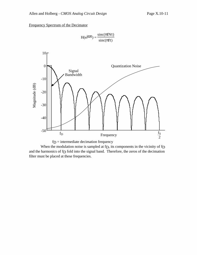
Allen and Holberg - CMOS Analog Circuit Design Page X.10-11
Frequency Spectrum of the Decimator
H(ejωτ) = sinc(πfNτ)
sinc(πfτ)
-50
-40
-30
-20
-10
0
10
fS2
Frequency
Mag
nitu
de (
dB)
fD
Quantization NoiseSignal
Bandwidth
fD = intermediate decimation frequencyWhen the modulation noise is sampled at fD, its components in the vicinity of fD
and the harmonics of fD fold into the signal band. Therefore, the zeros of the decimationfilter must be placed at these frequencies.

Allen and Holberg - CMOS Analog Circuit Design Page X.10-12
Digital Lowpass Filter
∑∆ MODULATOR
DECIMATORLOW-PASS
FILTER
analog input
fDfS
2fB
digital PCM
fB
FIR or IIR digital low pass filter
-110
-80
-50
-20
10
4000 Frequency (Hz)
Mag
nitu
de (
dB)
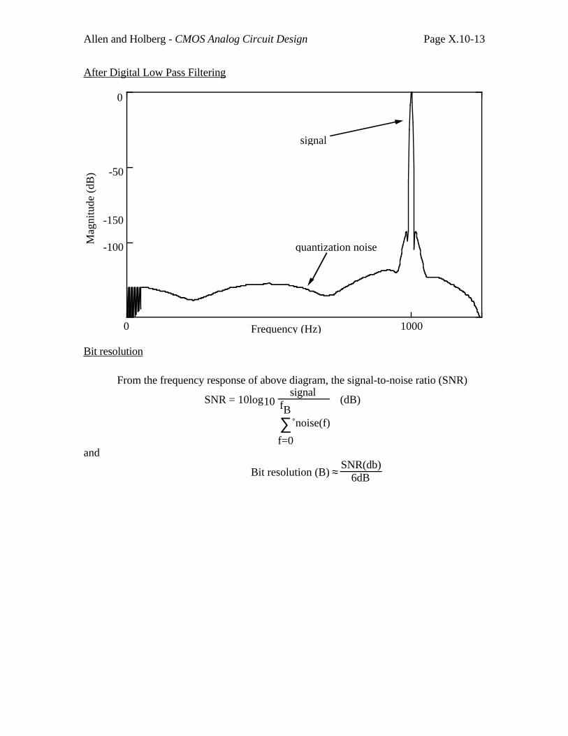
Allen and Holberg - CMOS Analog Circuit Design Page X.10-13
After Digital Low Pass Filtering
-150
Mag
nitu
de (
dB)
-100
-50
0
0 1000Frequency (Hz)
signal
quantization noise
Bit resolution
From the frequency response of above diagram, the signal-to-noise ratio (SNR)
SNR = 10log10 signal
∑f=0
fB noise(f)
(dB)
and
Bit resolution (B) ≈ SNR(db)
6dB
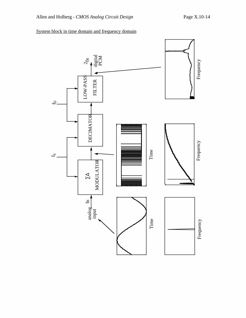
Allen and Holberg - CMOS Analog Circuit Design Page X.10-14
System block in time domain and frequency domain
∑
∆ M
OD
UL
AT
OR
DE
CIM
AT
OR
LO
W-P
ASS
FI
LT
ER
anal
og in
put
f Df S
2 fB
digi
tal
PC
M
f B
Tim
eT
ime
Freq
uenc
yFr
eque
ncy
Freq
uenc
y
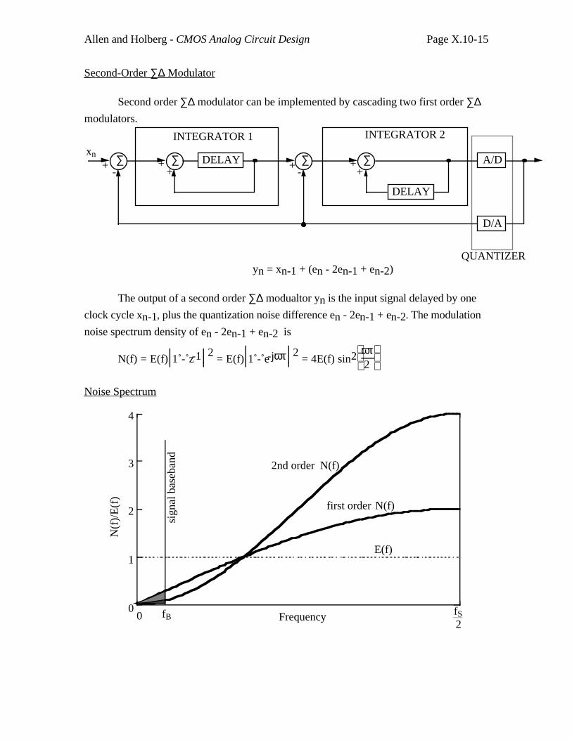
Allen and Holberg - CMOS Analog Circuit Design Page X.10-15
Second-Order ∑∆ Modulator
Second order ∑∆ modulator can be implemented by cascading two first order ∑∆modulators.
∑DELAY∑++
∑++
∑ +-
A/D
D/A
QUANTIZER
INTEGRATOR 1 INTEGRATOR 2
+-
xn yn
DELAY
yn = xn-1 + (en - 2en-1 + en-2)
The output of a second order ∑∆ modualtor yn is the input signal delayed by one
clock cycle xn-1, plus the quantization noise difference en - 2en-1 + en-2. The modulation
noise spectrum density of en - 2en-1 + en-2 is
N(f) = E(f) 1 - z-1 2
= E(f) 1 - e-jωτ 2
= 4E(f) sin2
ωτ
2
Noise Spectrum
fS2
0 Frequency
E(f)
N(f
)/E
(f)
sign
al b
aseb
and
fB
N(f)2nd order
first order N(f)
0
1
2
3
4
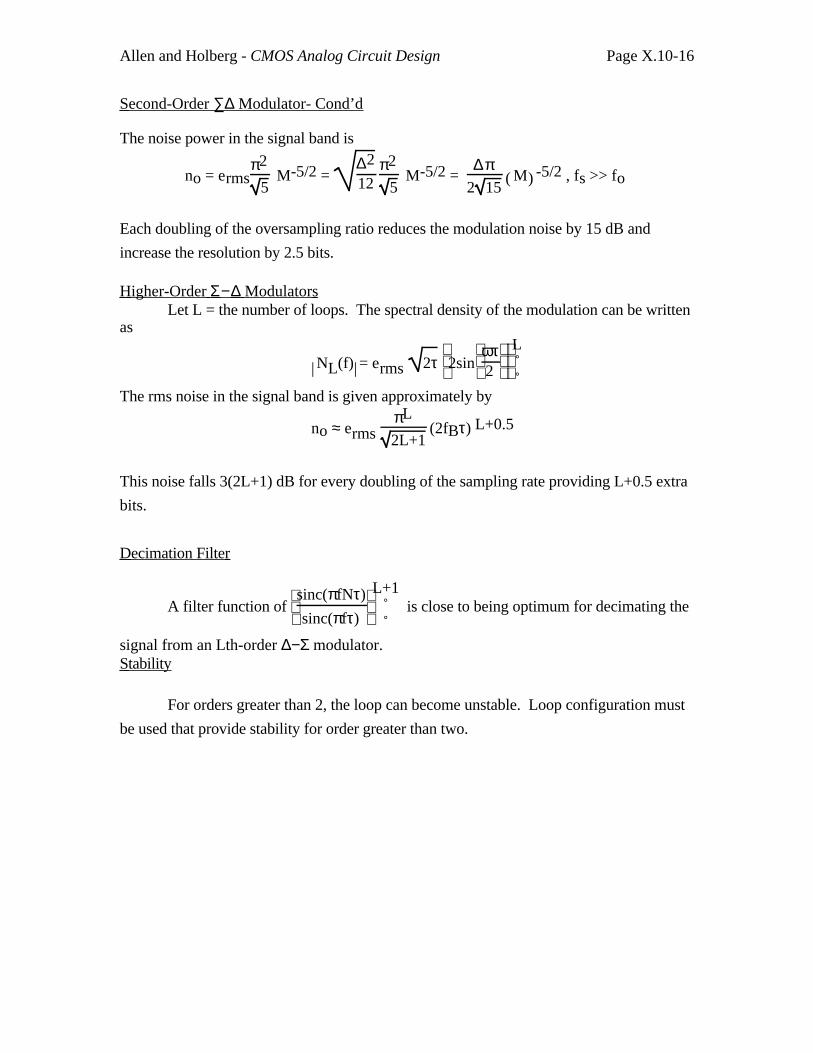
Allen and Holberg - CMOS Analog Circuit Design Page X.10-16
Second-Order ∑∆ Modulator- Cond’d
The noise power in the signal band is
no = ermsπ2
5 M-5/2 =
∆2
12 π2
5 M-5/2 =
∆π2 15
( )M -5/2 , fs >> fo
Each doubling of the oversampling ratio reduces the modulation noise by 15 dB and
increase the resolution by 2.5 bits.
Higher-Order Σ−∆ Modulators Let L = the number of loops. The spectral density of the modulation can be written
as
| |NL(f) = erms 2τ
2sin
ωτ
2
L
The rms noise in the signal band is given approximately by
no ≈ erms πL
2L+1 (2fBτ) L+0.5
This noise falls 3(2L+1) dB for every doubling of the sampling rate providing L+0.5 extra
bits.
Decimation Filter
A filter function of
sinc(πfNτ)
sinc(πfτ)
L+1
is close to being optimum for decimating the
signal from an Lth-order ∆−Σ modulator. Stability
For orders greater than 2, the loop can become unstable. Loop configuration must
be used that provide stability for order greater than two.
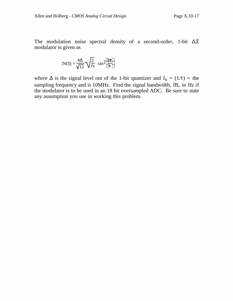
Allen and Holberg - CMOS Analog Circuit Design Page X.10-17
The modulation noise spectral density of a second-order, 1-bit ∆Σmodulator is given as
|N(f)| = 4∆12
2fs sin2
ωt
4
where ∆ is the signal level out of the 1-bit quantizer and fs = (1/τ) = thesampling frequency and is 10MHz. Find the signal bandwidth, fB, in Hz ifthe modulator is to be used in an 18 bit oversampled ADC. Be sure to stateany assumption you use in working this problem.
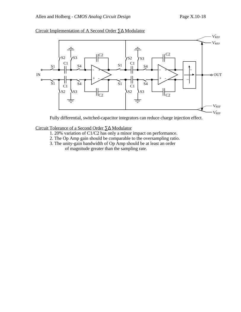
Allen and Holberg - CMOS Analog Circuit Design Page X.10-18
Circuit Implementation of A Second Order ∑∆ Modulator
-
-
+
+
-
-
+
+
S1
S1
S1
S1
S2
S2
S2
S2 S3
S3S3
S3
S4
S4
C2
C2
C1
C1 C1
C1S4
S4
C2
C2
VREF+
VREF+
VREF-
VREF-
OUTIN
Fully differential, switched-capacitor integrators can reduce charge injection effect.
Circuit Tolerance of a Second Order ∑∆ Modulator1. 20% variation of C1/C2 has only a minor impact on performance.2. The Op Amp gain should be comparable to the oversampling ratio.3. The unity-gain bandwidth of Op Amp should be at least an order
of magnitude greater than the sampling rate.
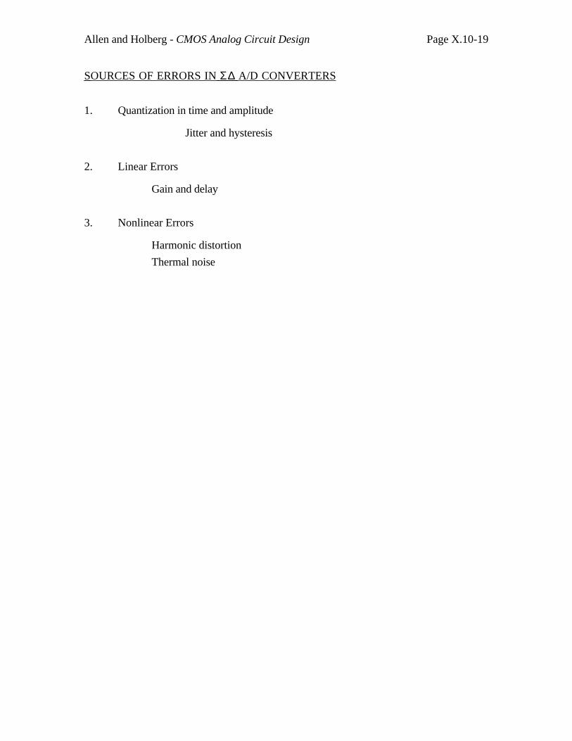
Allen and Holberg - CMOS Analog Circuit Design Page X.10-19
SOURCES OF ERRORS IN Σ∆ A/D CONVERTERS
1. Quantization in time and amplitude
Jitter and hysteresis
2. Linear Errors
Gain and delay
3. Nonlinear Errors
Harmonic distortion
Thermal noise
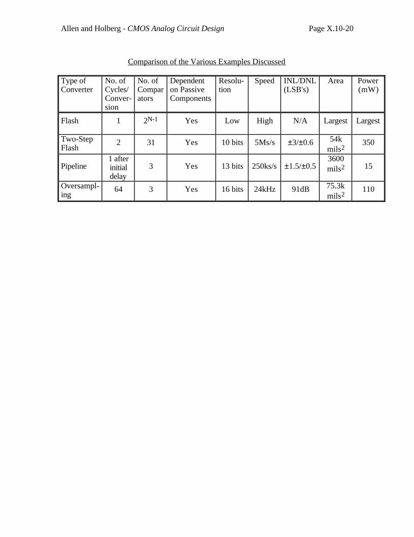
Allen and Holberg - CMOS Analog Circuit Design Page X.10-20
Comparison of the Various Examples Discussed
Type ofConverter
No. ofCycles/Conver-sion
No. ofComparators
Dependenton PassiveComponents
Resolu-tion
Speed INL/DNL(LSB's)
Area Power(mW)
Flash 1 2N-1 Yes Low High N/A Largest Largest
Two-StepFlash
2 31 Yes 10 bits 5Ms/s ±3/±0.6 54kmils2
350
Pipeline1 afterinitialdelay
3 Yes 13 bits 250ks/s ±1.5/±0.53600mils2 15
Oversampl-ing
64 3 Yes 16 bits 24kHz 91dB 75.3kmils2
110
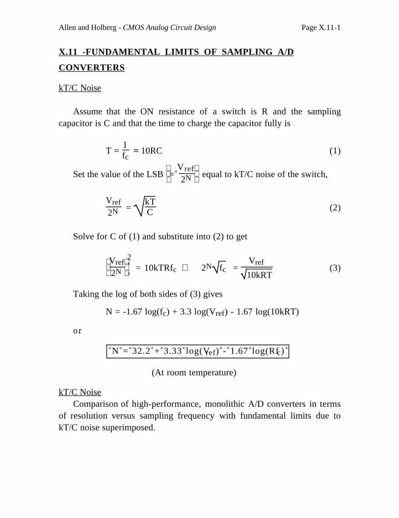
Allen and Holberg - CMOS Analog Circuit Design Page X.11-1
X.11 -FUNDAMENTAL LIMITS OF SAMPLING A/D
CONVERTERS
kT/C Noise
Assume that the ON resistance of a switch is R and the samplingcapacitor is C and that the time to charge the capacitor fully is
T = 1fc
≈ 10RC (1)
Set the value of the LSB
= Vref
2N equal to kT/C noise of the switch,
Vref
2N = kTC (2)
Solve for C of (1) and substitute into (2) to get
Vref
2N
2 = 10kTRfc ⇒ 2N fc =
Vref
10kRT (3)
Taking the log of both sides of (3) gives
N = -1.67 log(fc) + 3.3 log(Vref) - 1.67 log(10kRT)
or
N = 32.2 + 3.33 log(Vref) - 1.67 log(Rfc)
(At room temperature)
kT/C Noise Comparison of high-performance, monolithic A/D converters in terms
of resolution versus sampling frequency with fundamental limits due tokT/C noise superimposed.
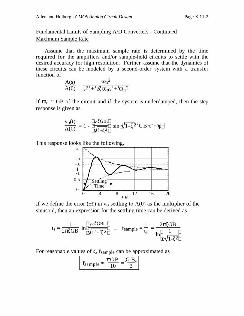
Allen and Holberg - CMOS Analog Circuit Design Page X.11-2
Fundamental Limits of Sampling A/D Converters - Continued Maximum Sample Rate
Assume that the maximum sample rate is determined by the timerequired for the amplifiers and/or sample-hold circuits to settle with thedesired accuracy for high resolution. Further assume that the dynamics ofthese circuits can be modeled by a second-order system with a transferfunction of
A(s)A(0) =
ωn2
s2 + 2ζωns + ωn2
If ωn ≈ GB of the circuit and if the system is underdamped, then the stepresponse is given as
vo(t)A(0) = 1 -
e-ζGBt
1-ζ2 sin 1-ζ 2 GB·t + φ
This response looks like the following,
0
0.5
1
1.5
2
0 4 8 12 16 20
+ε
-ε
SettlingTime
ωnt
If we define the error (±ε) in vo settling to A(0) as the multiplier of thesinusoid, then an expression for the settling time can be derived as
ts = 1
2πζGB ln
e-ζGBt
1 - ζ 2 ⇒ fsample =
1ts
= 2πζGB
ln
1
ε 1-ζ2
For reasonable values of ζ, fsample can be approximated as
fsample ≈ πG B
10 = G B
3
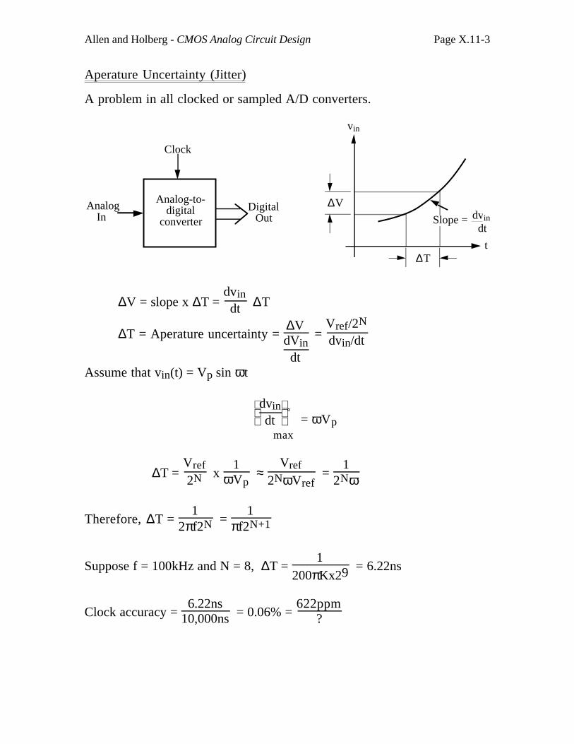
Allen and Holberg - CMOS Analog Circuit Design Page X.11-3
Aperature Uncertainty (Jitter)
A problem in all clocked or sampled A/D converters.
Analog-to-digital
converter
AnalogIn
Digital Out
Clock
vin
∆V
Slope = dvindt
t∆T
∆V = slope x ∆T = dvindt ∆T
∆T = Aperature uncertainty = ∆VdVin
dt
= Vref/2N
dvin/dt
Assume that vin(t) = Vp sin ωt
dvin
dt
max = ωVp
∆T = Vref
2N x 1
ωVp ≈
Vref
2NωVref =
12Nω
Therefore, ∆T = 1
2πf2N = 1
πf2N+1
Suppose f = 100kHz and N = 8, ∆T = 1
200πKx29 = 6.22ns
Clock accuracy = 6.22ns
10,000ns = 0.06% = 622ppm
?
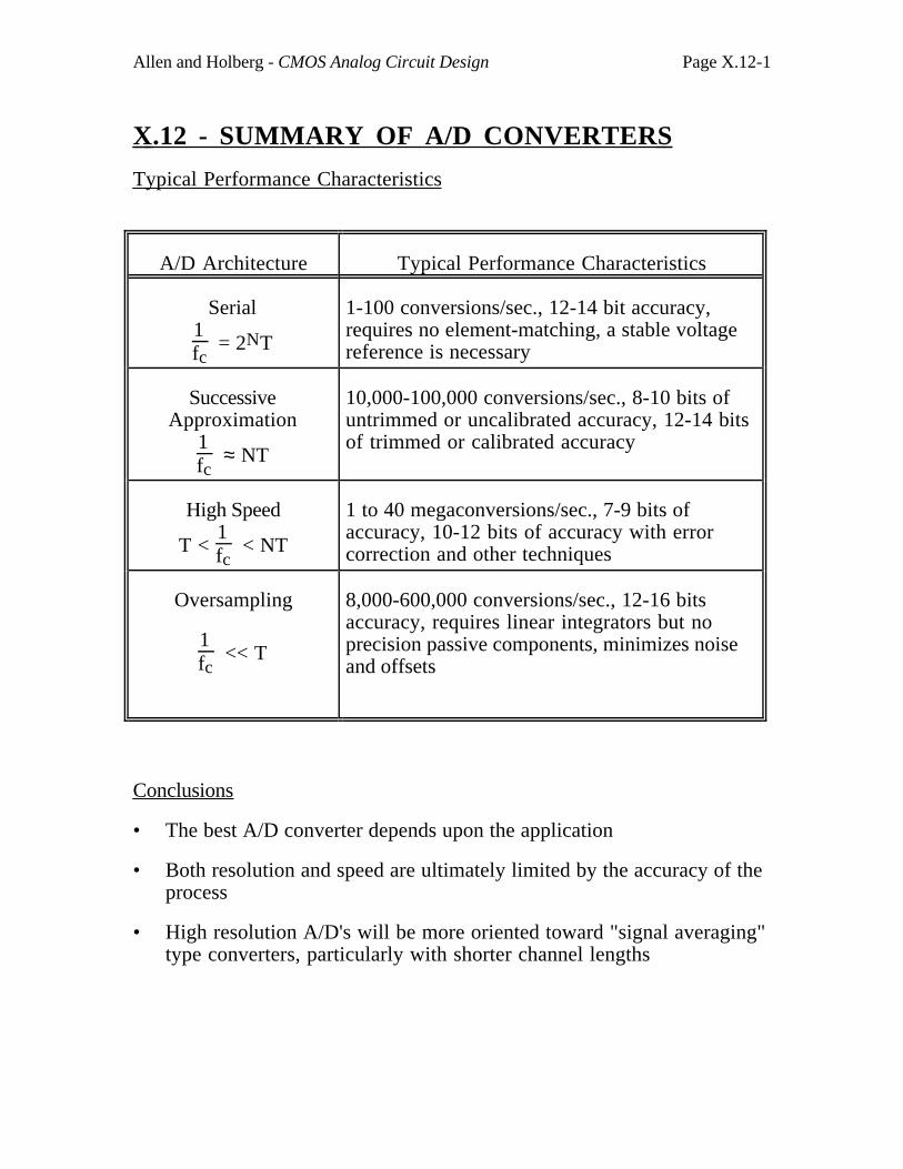
Allen and Holberg - CMOS Analog Circuit Design Page X.12-1
X.12 - SUMMARY OF A/D CONVERTERS
Typical Performance Characteristics
A/D Architecture Typical Performance Characteristics
Serial1fc
= 2NT
1-100 conversions/sec., 12-14 bit accuracy,requires no element-matching, a stable voltagereference is necessary
SuccessiveApproximation
1fc
≈ NT
10,000-100,000 conversions/sec., 8-10 bits ofuntrimmed or uncalibrated accuracy, 12-14 bitsof trimmed or calibrated accuracy
High Speed
T < 1fc
< NT
1 to 40 megaconversions/sec., 7-9 bits ofaccuracy, 10-12 bits of accuracy with errorcorrection and other techniques
Oversampling
1fc
<< T
8,000-600,000 conversions/sec., 12-16 bitsaccuracy, requires linear integrators but noprecision passive components, minimizes noiseand offsets
Conclusions
• The best A/D converter depends upon the application
• Both resolution and speed are ultimately limited by the accuracy of theprocess
• High resolution A/D's will be more oriented toward "signal averaging"type converters, particularly with shorter channel lengths