aic111 datasheet pdf - texas instruments · total harmonic distortion 100 hz-10khz, 40- block...
TRANSCRIPT

AIC111
www.ti.com SLAS382A –JUNE 2003–REVISED NOVEMBER 2005
IC DESIGN SPECIFICATION1.3-V microPower™ DSP/μC VOICE BAND AUDIO CODEC
Check for Samples: AIC111
1FEATURES – - 32-Pin QFN 5×5-mm Plastic Package– - 32-Pad Bumped Die in Waffle Pack (wafer
2• Single Channel Codecscale packaging)• Noise Shaped Delta Sigma ADC and DAC
TechnologyAPPLICATIONS
• Low Supply Voltage and Current:• Hearing Instruments– 1.3-V Typical Power Supply• Personal Medical Devices– 350-µA Typical Supply Current Drain• Hearing Protection• Power Supply Up Monitor and Low Battery• Aural ProcessingMonitor That Also Automatically Shuts Off H-
Bridge Output When Battery Decays Below • Low-Power Headsets1.05 V in a Nontransient Manner
DESCRIPTION• Typical 2.4-µVrms Input Referred Noise WithThe AIC111 IC design specification serves to provide0.01% Total Harmonic Distortion for Front Endproduct development teams with a guideline for howand 108-dB Dynamic Rangethe AIC111 IC is specified and programmable options• ADC Has 87-dB Dynamic Range With 73-dB that are available. The document outlines a top-level
Total Harmonic Distortion 100 Hz-10 kHz, 40- block description of the IC along with systemkHz Sampling Rate specifications and functions. Individual block
• Typical 55-dB PSRR 100 Hz to 10 kHz for descriptions and target specifications are alsooutlined.Analog Front End
• Low Noise Programmable Gain The Texas Instruments AIC111 is a TI µPower DSPAmplifier/Compressor Front End With compatible, or microcontroller compatible audio
codec product, or analog interface circuit. TheProgrammable Fast and Slow Attack andAIC111 is part of a comprehensive family of DSP/µCDecay Rates With Dual or Single Attack andbased high-performance analog interface solutions.Decay Rate OptionThe AIC111 is targeted primarily at personal medical• Typical Output Noise of 12 µVrms With 0.05% devices, such as hearing instruments, aural
Total Harmonic Distortion for Delta Sigma DAC preprocessing applications, and low-power headsetand H-Bridge Output Driver applications. The AIC111 is used in any design
• Low Jitter Oscillator That Generates all requiring a programmable time constantPGA/compressor interface, high dynamic rangeInternal Clocks and Generates 5-MHz Outputanalog-to-digital converter, an external DSP/µCDSP/µC Clockhandling signal processing, or a low distortion digital-• Regulated Bandgap Voltage Reference to-analog converter with a balanced H-Bridge
• Programmable Functionality via Digital Serial speaker driver. It supports a CMOS digital interfaceInterface tailored for TI DSPs with the McBSP protocol such as
TMS320VC54x™ DSP family and SPI-based– McBSP Interface, DSP Protocolcontrollers such as TI MSP430x family of– TI TMS320VC54x™, TMS320VC55x™ DSPs microcontrollers. The AIC111 also has an external
– SPI Interface, Microcontroller Protocol microphone or sensor supply and bias and powersupply up low-battery monitor indicator.– TI MSP430xx
• External Chip Power Down and Reset• Available in:
1
Please be aware that an important notice concerning availability, standard warranty, and use in critical applications ofTexas Instruments semiconductor products and disclaimers thereto appears at the end of this data sheet.
2microPower is a trademark of Texas Instruments.
UNLESS OTHERWISE NOTED this document contains Copyright © 2003–2005, Texas Instruments IncorporatedPRODUCTION DATA information current as of publication date.Products conform to specifications per the terms of TexasInstruments standard warranty. Production processing does notnecessarily include testing of all parameters.
AIC111
SLAS382A –JUNE 2003–REVISED NOVEMBER 2005 www.ti.com
These devices have limited built-in ESD protection. The leads should be shorted together or the device placed in conductive foam duringstorage or handling to prevent electrostatic damage to the MOS gates.
This integrated circuit can be damaged by ESD. Texas Instruments recommends that all integrated circuits be handled withappropriate precautions. Failure to observe proper handling and installation procedures can cause damage.
ESD damage can range from subtle performance degradation to complete device failure. Precision integrated circuits may be moresusceptible to damage because very small parametric changes could cause the device not to meet its published specifications.
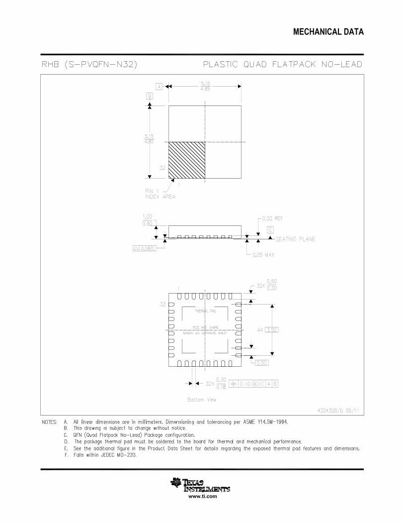
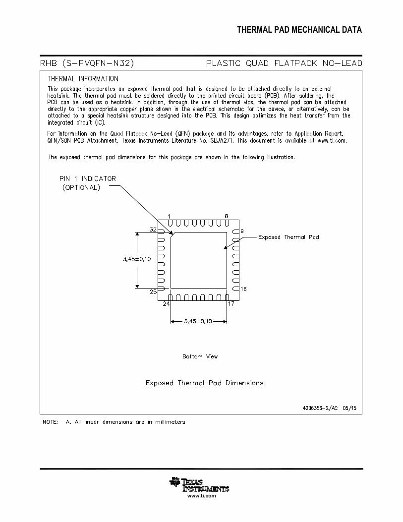
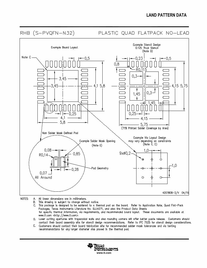
The AIC111 comes in a 32-pin QFN 5×5-mm package. A 32-pad solder ball bumped flip chip die that comes inwaffle packs or tape and reel is in preview and will be available 3rd quarter 2003.
AVAILABLE OPTIONS (1)
Part Number Package
AIC111RHB 32-pin QFN (5 mm x 5 mm), in tube.
AIC111RHBR 32-pin QFN (5 mm x 5 mm), tape and reel
AIC111YE 32-pad waffle scale chip package, bumped die in waffle pack (commercial)
AIC111YE 32-pad waffle scale chip package, bumped die in waffle pack (industrial)
AIC111YER 32-pad (WSCP) bumped die in tape and reel
(1) For the most current package and ordering information, see the Package Option Addendum at the end of this document, or see the TIwebsite at www.ti.com.
ABSOLUTE MAXIMUM RATINGSover operating free-air temperature range unless otherwise noted( (1))( (2))
UNIT
Input voltage AI or DI pins -0.3 V to 4 V
Power supply VDD, power pins -0.3 V to 4.5 V
Latch-up tolerance JEDEC latch-up (EIA/JEDS78) 100 mA
Commerical 0°C to 70°CTA Operating free-air temperature range,
Industrial −40°C to 85°C
Functional temperature range -15°C to 85°C
Reflow temperature range (flip chip) 220°C to 230°C
Tstg Storage temperature range -40°C to 125°C
Storage humidity 65% R.H.
(1) Stresses beyond those listed under absolute maximum ratings may cause permanent damage to the device. These are stress ratingsonly, and functional operation of the device at these or any other conditions beyond those indicated under recommended operatingconditions is not implied. Exposure to absolute-maximum-rated conditions for extended periods may affect device reliability.
(2) Specifications are assured operating at maximum device limits for QFN package only, unless otherwise specified.
ELECTRICAL CHARACTERISTICSINPUT/OUTPUT, OPERATING TEMPERATURE AT 25°C
PARAMETER TEST CONDITION MIN TYP MAX UNIT
Digital interface (see (1) and (2)) BUF_DVDD (see Note (1)) 3.6 V
BUF_DVDD-VIH High-level input voltage V0.2
BUF_DVSS+VIL Low-level input voltage V0.2
VOH High-level output voltage BUF_DVDD V
VOL Low-level output voltage BUF_DVSS V
Maximum allowed input voltage (AVIN) Differential 450 mVpk
(1) DVDD, VDD_OSC, and AVDD should be within 50 mV, preferably connected together. AVSS1, 2, DVSS, and VSS_OSC should bewithin 50 mV, preferably connected together.
(2) Maximum (0.9 V, DVDD -0.5 V) ≤ BUF_DVDD ≤3.6 V
2 Copyright © 2003–2005, Texas Instruments Incorporated

AIC111
www.ti.com SLAS382A –JUNE 2003–REVISED NOVEMBER 2005
ELECTRICAL CHARACTERISTICS (continued)INPUT/OUTPUT, OPERATING TEMPERATURE AT 25°C
PARAMETER TEST CONDITION MIN TYP MAX UNIT
Input impedance (AVIN) (see (3)) Nominal gain = 50x 20 kΩInput capacitance (AVIN) 5 pF
Microphone bias voltage (MIC_VSUP) 20-μA maximum 0.87 0.94 0.99 V
Microphone bias resistor (MIC_BIAS) 27 29.1 31 kΩFixed Q 3/4 HB_VDDDAC full scale outputH-bridge amplifier output VPPdifferential Adaptive Q HB_VDD
Output resistance Differential, HB - VDD = 1.3 V 20 or 40 Ω
(3) Driving single-ended: Rin = R × [(1+A)/(2+A)], A = PGAC Gain (linear), R = 20.4 kΩ for A ≥4 or 20.4 kΩ× (4/A) for A<4.Rin(min) = 17 kΩ(A=4), Rin(max) = 59.89 kΩ (A = 0.89), Rin(nom) = 20 kΩ (A = 50).
Copyright © 2003–2005, Texas Instruments Incorporated 3
Bumped Side
Bumped View
SU
B_V
SS
AIC111
HB
_VD
D
4
1
2
3
5
6
78
VMID_FILT
AVSS1
AVSS2
VREF
AVINM
AVINP
MIC_BIAS
MIC_VSUP16
VD
D_O
SC
VO
UT
_P
17
18
19
HB
_VS
S_P
VO
UT
_M
HB
_VS
S_M
22
20
21
SC
LK
FRAME
VR
FIL
T
AV
SS
_RE
F
AV
DD
28 27 2625
24
2930
23
9 10 11 12 13 14
EX
T_R
ST
/PW
DN
DVSS1
15
DVDD
VS
S_O
SC
IMODE
MCLK
BUF_DVDD
BUF_DVSS
SDOUT
SDIN
3132
RS
T/L
BM
Back Side
PCB ViewFor exact bump
location see Spec.Section 2.2
SU
B_V
SS
AIC111
HB
_VD
D
4
1
2
3
5
6
78
VMID_FILT
AVSS1
AVSS2
VREF
AVINM
AVINP
MIC_BIAS
MIC_VSUP16
VD
D_O
SC
VO
UT
_P
17
18
19
HB
_VS
S_P
VO
UT
_MH
B_V
SS
_M
22
20
21
SC
LK
DV
SS
2
FRAME
VR
FILT
AV
SS
_RE
F
AV
DD
28 27 2625
24
2930
23
9 10 11 12 13 14
EX
T_R
ST
/PW
DN
DVSS1
15
DVDD
VS
S_O
SC
IMODE
MCLK
BUF_DVDD
BUF_DVSS
SDOUT
SDIN
3132
RS
T/L
BM
AlignmentMarker
(0,0)
DV
SS
2
AIC111
SLAS382A –JUNE 2003–REVISED NOVEMBER 2005 www.ti.com
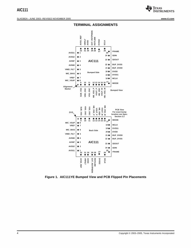
TERMINAL ASSIGNMENTS
Figure 1. AIC111YE Bumped View and PCB Flipped Pin Placements
4 Copyright © 2003–2005, Texas Instruments Incorporated
1
2
3
4
5
6
7
89 10 11 12 13 14 15 16
17
18
19
20
21
22
23
24
2526272829303132
VD
D_O
SC
VS
S_O
SC
SU
B_V
SS
MCLK
DVDD
MIC_VSUP
AVSS1
AVINM
AVINP
AVSS2
VR
FIL
T
AV
SS
_RE
F
VREF_BG
AV
DD
DV
SS
DVSS
VMID_FILT
MIC_BIAS
IMODE
SDOUT
FR
AM
E
SDIN
SC
LK
BUF_DVDD
RS
T/L
BM
HB
_VS
S_M
VO
UT
_M
HB
_VD
D
VO
UT
_P
HB
_VS
S_P
BUF_DVSS
DV
SS
AIC111RHB
AIC111
www.ti.com SLAS382A –JUNE 2003–REVISED NOVEMBER 2005
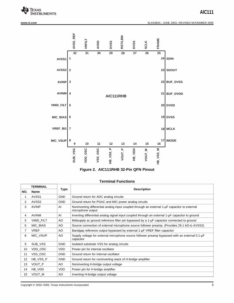
Figure 2. AIC111RHB 32-Pin QFN Pinout
Terminal FunctionsTERMINAL
Type DescriptionNO. Name
1 AVSS1 GND Ground return for ADC analog circuits
2 AVSS2 GND Ground return for PGAC and MIC power analog circuits
3 AVINP AI Noninverting differential analog input coupled through an external 1-μF capacitor to externalmicrophone output
4 AVINM AI Inverting differential analog signal input coupled through an external 1-μF capacitor to ground
5 VMID_FILT AO Midsupply ac ground reference filter pin bypassed by a 1-μF capacitor connected to ground
6 MIC_BIAS AO Source connection of external microphone source follower preamp. (Provides 29.1 kΩ to AVSS2)
7 VREF AO Bandgap reference output bypassed by external 1-μF VREF filter capacitor
8 MIC_VSUP AO Supply voltage for external microphone source follower preamp bypassed with an external 0.1-μFcapacitor
9 SUB_VSS GND Isolated substrate VSS for analog circuits
10 VDD_OSC VDD Power pin for internal oscillator
11 VSS_OSC GND Ground return for internal oscillator
12 HB_VSS_P GND Ground return for noninverting stack of H-bridge amplifier
13 VOUT_P AO Noninverting H-bridge output voltage
14 HB_VDD VDD Power pin for H-bridge amplifier
15 VOUT_M AO Inverting H-bridge output voltage
Copyright © 2003–2005, Texas Instruments Incorporated 5

DVDDMIC_VSUP
VREF
DVSSMIC_BIAS
IMO
DE
SD
OU
T
FR
AM
E
SD
IN
SC
LK
BUF_DVDD
BUF_DVSS
DigitalInterface
Output BuffersVDD_OSC
VSS_OSC
MC
LK
RST/LBM
Oscillator
PORMIC/SensorPower and
Bias
BandgapReference
BiasesGenerator
HB
_VS
S_M
VOUT_M
HB
_VD
DVOUT_P
HB
_VS
S_P
DeltaSigmaDAC
H-BridgeSpeakerDriver
SU
B_V
SS
AV
SS
AVINM
AVINP
VR
FIL
T
AV
SS
_RE
F
AV
DD
VM
ID_F
ILT
PGA/Compressor RCFlt
DeltaSigmaADC
Dec.Filter
&HPF
EX
T_R
ST
/PW
DN
AIC111
SLAS382A –JUNE 2003–REVISED NOVEMBER 2005 www.ti.com
Terminal Functions (continued)
TERMINALType Description
NO. Name
16 HB_VSS_M GND Ground return for inverting stack of H-bridge amplifier
17 IMODE DI Digital interface format selection pin
18 MCLK DO 5-MHz output clock for external DSP/μC
19 DVSS1 GND Ground return for digital circuits
20 DVDD VDD Power pin for digital circuits
21 BUF_DVDD VDD Power pin for interface digital I/O circuits
22 BUF_DVSS GND Ground return for interface digital I/O circuits
23 SDOUT DO Digital interface serial data output pin
24 SDIN DI Digital interface serial data input pin
25 FRAME DO Digital interface serial data framer
26 SCLK DO Digital interface serial shift clock
27 DVSS2 GND Ground return for digital circuits
28 RST/LBM DO Provides external reset and low battery monitor
29 EXT_RST/PWDN DI Powers down all analog blocks and holds digital outputs low until internal system is up
30 AVDD VDD VDD power pin for analog circuits
31 VRFILT AO Positive ADC reference pin bypassed with 1-μF capacitor to AVSS_REF
32 AVSS_REF GND Ground for ADC voltage reference
Figure 3. FUNCTIONAL BLOCK DIAGRAM
OPERATION
The power source may be a zinc-air battery operating at a typical voltage of 1.3 V. A single external de-couplingcapacitor of 1 μF is recommended on the main power supply.
6 Copyright © 2003–2005, Texas Instruments Incorporated

-100
-90
-80
-70
-60
-50
-40
-30
-20
-10
0
0 10 20 30 40 50 60 70 80 90 100f - Frequency - kHz
Gai
n -
dB
-20
-18
-16
-14
-12
-10
-8
-6
-4
-2
0
0 2 4 6 8 10 12 14 16 18 20
f - Frequency - kHz
Gai
n -
dB
AIC111
www.ti.com SLAS382A –JUNE 2003–REVISED NOVEMBER 2005
VOLTAGE and CURRENT, OPERATING TEMPERATURE AT 25°C
PARAMETER TEST CONDITION MIN TYP MAX UNIT
AVDD, DVDD (All pins of type AVDD, DVDD Steady-state battery supply 1.1 1.3 1.5 Vin pin-out table)
• Unloaded: H-Bridge output open• Microphone resistor model connected (see
IS (supply current) Figure 5) 350 μA• Power supplies = 1.3 V• No receiver attached
FUNCTIONAL INPUT CHANNEL PERFORMANCE REQUIREMENTS
The front end is defined as the differential signal path from the PGA/compressor inputs, AVINP, and AVINMthrough the delta-sigma ADC and decimation filter.
Typical Conditions; deviations are noted in table.• Operating Temperature Range: 0°C to 70°C. All specification are at 25°C and 1.3 V unless otherwise noted.• AVDD, DVDD range: 1.1 V to 1.5 V• AVINP, AVINM inputs: AC coupled, Frequency ranging from 100 Hz-10 kHz• Measurement Bandwidth: 100 Hz-10 kHz A-weighted.• Idle channel definition: AVINP and AVINM are both ac-coupled to AVSS.• Typical PGAC gain range is -1 dB to 40 dB.• Maximum input voltage: 450 mVpk.
PARAMETER TEST CONDITION MIN TYP MAX UNIT
Broad-band noise Input referred idle channel 2.4 μV RMS
THD (low level) AVIN≤ PGAC threshold(see Note (1)) 0.01 0.2%
DC Offset Idle channel -5 0 5 mV
Droop at 10 kHz Referenced to amplitude at 1 kHz 1.2 dB
(1) PGAC threshold = PGAC threshold voltage/maximum gain of PGAC.
Figure 4. Input Channel Frequency Response With HPF Bypassed
Copyright © 2003–2005, Texas Instruments Incorporated 7
AIC111
SLAS382A –JUNE 2003–REVISED NOVEMBER 2005 www.ti.com
ANALOG-TO-DIGITAL CONVERTER FILTERED INPUT VOLTAGE REFERENCE
Function - Filters analog supply AVDD for DS-ADC reference. With a recommended 0.1-μF external capacitorbetween pins VRFILT and AVSS_REF, the pole is set at approximately 72 Hz, with 1 μF, the pole is set atapproximately 7 Hz.
PROGRAMMABLE GAIN AMPLIFIER AND COMPRESSOR
Function:
The programmable gain amplifier and compressor (PGAC) amplifies the microphone or sensor output signal,provides an appropriate impedance to the microphone buffer or sensor, and provides input gain compressionlimiting depending on the input signal level if one is not using the fixed gain mode, where the PGAC gain is setby selected register bits. Input compression limiting is discrete automatic gain correction (AGC) based ondetecting the peak input signal level using a peak detector circuit that has programmable time responses toprovide AGC control, and is intended to prevent a steady state input level up to the defined PGAC limit frombeing clipped. The attack/release times of the PGAC are programmable by internal clock selection inside thePGAC digital level circuitry that affects the rate of gain changes.
The PGAC has four modes of operation: automatic dual-rate (default), automatic single-rate, fixed single-rate,and fixed immediate. Mode selection is controlled by bits 3 and 2 of the PDCREG register.
AUTOMATIC DUAL-RATE MODE (00, DEFAULT):
In this mode of operation, the PGAC has two attack (gain decrease) rates and two release (gain increase) rates,which may be selected by programming the FASTARREG and FORMAT4 registers. Internally, two counters areused to control the compressor gain. The fast rate counter responds at the fast attack and release rates, and itcounts down at the attack rate to decrease the PGAC gain if the output of the PGAC is instantaneously largerthan a preset threshold (PGAC_THRES = 400-mV peak), or it counts up to increase the gain, up to the maximumallowed gain as set by the PGACREG register, if the output of the PGAC falls below a second threshold, which is3 dB lower (283-mV peak), which provides hysteresis. Before the gain is allowed to increase, the signal at theoutput of the PGAC must be below the lower threshold for a period of time which is controlled by bit 4 ofPDCREG, and can be 50 ms (0, default) or 25 ms (1). The slow-rate counter responds at the slow attack andrelease rates, and it attempts to track the state of the fast rate counter. The PGAC gain is determined bywhichever counter is smaller. In this way, the PGAC can respond and recover rapidly to short signal bursts whileresponding more slowly to the signal average.
AUTOMATIC SINGLE-RATE MODE (01):
In this mode of operation, the PGAC has one attack rate and one release rate, which may be selected byprogramming the FASTARREG register. The operation of the PGAC is similar to the dual-rate mode, except thatthe slow-rate counter is disabled and the PGAC gain is solely determined by the fast-rate counter.
FIXED SINGLE-RATE MODE (10):
In this mode of operation, the PGAC gain tracks the value specified in the PGACREG register regardless of thesignal amplitude, and changes in PGACREG cause the gain to decrease or increase at the corresponding fastattack or release rate specified in the FASTARREG register.
FIXED IMMEDIATE MODE (11):
In this mode of operation, the PGAC gain tracks the value specified in the PGACREG register regardless of thesignal amplitude, and changes in PGACREG cause the gain to change immediately to the desired gain withoutstepping through the intermediate gain states.
Bit 7 of the PGACREG register controls the PGAC gain read mode. While this bit is low (default), readingPGACREG returns the contents of PGACREG. However, if this bit is set high, then any subsequent read(s) ofPGACREG returns the actual, instantaneous PGAC gain. This information may be useful, for example, fordynamic range expansion, effectively undoing the compression effect in the automatic modes of operation.
CHARACTERISTICS
: Compression limits the PCAG output. PGACREG is a programmable register.
8 Copyright © 2003–2005, Texas Instruments Incorporated
AIC111
www.ti.com SLAS382A –JUNE 2003–REVISED NOVEMBER 2005
SPECIFICATIONS AT 25°C, AVDD = 1.3 V (2) (3)
PARAMETER TEST CONDITIONS MIN TYP MAX UNIT
Input Signal Parameters
Maximum signal swing Gain = -1 dB 900 mVPP
Block Parameters
Gain size step 0.3 0.5 0.7 dB
(2) Based on a system clock of 1.280 MHz.(3) For fixed gain mode the rate is 80 KdB/s to new programmed value of gain. All intermediate 0.5 dB gain steps are passed through to
reach new gain.
DELTA SIGMA A/D CONVERTER/ANTI-ALIAS FILTER
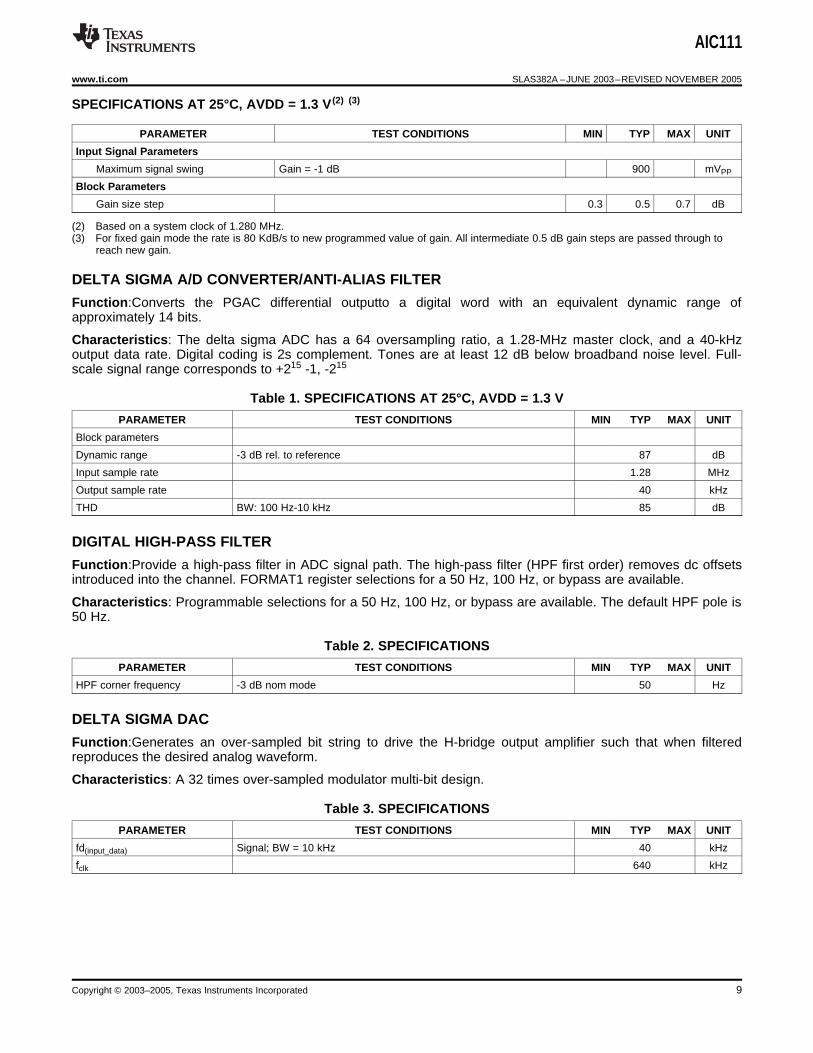
Function:Converts the PGAC differential outputto a digital word with an equivalent dynamic range ofapproximately 14 bits.
Characteristics: The delta sigma ADC has a 64 oversampling ratio, a 1.28-MHz master clock, and a 40-kHzoutput data rate. Digital coding is 2s complement. Tones are at least 12 dB below broadband noise level. Full-scale signal range corresponds to +215 -1, -215
Table 1. SPECIFICATIONS AT 25°C, AVDD = 1.3 V
PARAMETER TEST CONDITIONS MIN TYP MAX UNIT
Block parameters
Dynamic range -3 dB rel. to reference 87 dB
Input sample rate 1.28 MHz
Output sample rate 40 kHz
THD BW: 100 Hz-10 kHz 85 dB
DIGITAL HIGH-PASS FILTER
Function:Provide a high-pass filter in ADC signal path. The high-pass filter (HPF first order) removes dc offsetsintroduced into the channel. FORMAT1 register selections for a 50 Hz, 100 Hz, or bypass are available.
Characteristics: Programmable selections for a 50 Hz, 100 Hz, or bypass are available. The default HPF pole is50 Hz.
Table 2. SPECIFICATIONS
PARAMETER TEST CONDITIONS MIN TYP MAX UNIT
HPF corner frequency -3 dB nom mode 50 Hz
DELTA SIGMA DAC
Function:Generates an over-sampled bit string to drive the H-bridge output amplifier such that when filteredreproduces the desired analog waveform.
Characteristics: A 32 times over-sampled modulator multi-bit design.
Table 3. SPECIFICATIONS
PARAMETER TEST CONDITIONS MIN TYP MAX UNIT
fd(input_data) Signal; BW = 10 kHz 40 kHz
fclk 640 kHz
Copyright © 2003–2005, Texas Instruments Incorporated 9
H-Bridge Load Switching
ReceiverOUTP OUTM
VDD (vbat)
AVSS
OUTPM
OUTMPOUTPP
OUTMM
VDD ( vbat)
AVSS
OUTPM
OUTMP OUTPP
OUTMM
Inverting Phase
OUTP OUTM
Noninverting Phase
LoadReceiver
Load
AIC111
SLAS382A –JUNE 2003–REVISED NOVEMBER 2005 www.ti.com
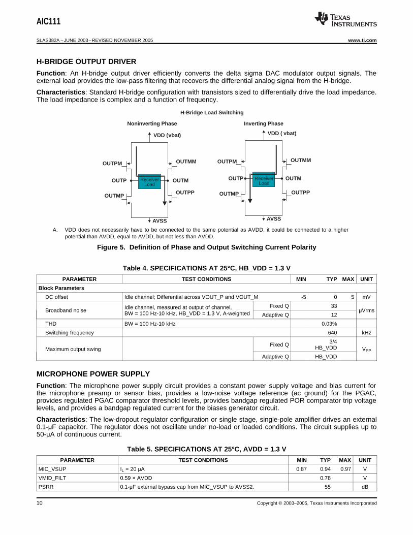
H-BRIDGE OUTPUT DRIVER
Function: An H-bridge output driver efficiently converts the delta sigma DAC modulator output signals. Theexternal load provides the low-pass filtering that recovers the differential analog signal from the H-bridge.
Characteristics: Standard H-bridge configuration with transistors sized to differentially drive the load impedance.The load impedance is complex and a function of frequency.
A. VDD does not necessarily have to be connected to the same potential as AVDD, it could be connected to a higherpotential than AVDD, equal to AVDD, but not less than AVDD.
Figure 5. Definition of Phase and Output Switching Current Polarity
Table 4. SPECIFICATIONS AT 25°C, HB_VDD = 1.3 V
PARAMETER TEST CONDITIONS MIN TYP MAX UNIT
Block Parameters
DC offset Idle channel; Differential across VOUT_P and VOUT_M -5 0 5 mV
Fixed Q 33Idle channel, measured at output of channel,Broadband noise μVrmsBW = 100 Hz-10 kHz, HB_VDD = 1.3 V, A-weighted Adaptive Q 12
THD BW = 100 Hz-10 kHz 0.03%
Switching frequency 640 kHz
3/4Fixed Q HB_VDDMaximum output swing VPP
Adaptive Q HB_VDD
MICROPHONE POWER SUPPLY
Function: The microphone power supply circuit provides a constant power supply voltage and bias current forthe microphone preamp or sensor bias, provides a low-noise voltage reference (ac ground) for the PGAC,provides regulated PGAC comparator threshold levels, provides bandgap regulated POR comparator trip voltagelevels, and provides a bandgap regulated current for the biases generator circuit.
Characteristics: The low-dropout regulator configuration or single stage, single-pole amplifier drives an external0.1-μF capacitor. The regulator does not oscillate under no-load or loaded conditions. The circuit supplies up to50-μA of continuous current.
Table 5. SPECIFICATIONS AT 25°C, AVDD = 1.3 V
PARAMETER TEST CONDITIONS MIN TYP MAX UNIT
MIC_VSUP IL = 20 μA 0.87 0.94 0.97 V
VMID_FILT 0.59 × AVDD 0.78 V
PSRR 0.1-μF external bypass cap from MIC_VSUP to AVSS2. 55 dB
10 Copyright © 2003–2005, Texas Instruments Incorporated
AIC111
www.ti.com SLAS382A –JUNE 2003–REVISED NOVEMBER 2005
Table 5. SPECIFICATIONS AT 25°C, AVDD = 1.3 V (continued)
PARAMETER TEST CONDITIONS MIN TYP MAX UNIT
Output impedance 1.5 kΩ
MCLK Output
Function: Provides a clock signal for external use.
Table 6. SPECIFICATIONS AT 25°C, VDD_OSC, DVDD, BUF_DVDD = 1.3 V
PARAMETER TEST CONDITIONS MIN TYP MAX UNIT
Frequency 4.7 5.12 5.5 MHz
Jitter RMS jitter 150 ps
Duty cycle 50%
POWER-ON RESET
Function:Provides a reset signal upon power up (stable voltage reference) that initializes the digital interface. Italso provides a gating signal to the delta-sigma DAC modulator to prevent audible pops and clicks fromerroneous data sent to the H-bridge circuit at power up and during periods when battery voltage has degradedbelow 1.05 V for an extended period of time (typically greater than 44 μs). The reset signal is asynchronous toMCLK. Digital interface does not start operating until after t(VDD)_valid has transpired.
POR has to:• Deal with system's on/off switch bounce lasting 100 ms or less.• Detect when the power supply AVDD is ≥1.1 V to enable the H-bridge output.• Provide kick-start to oscillator.• Detect when VDD degrades below 1.05 V for a period of time that is nontransient, and gate H-bridge output.
Table 7. SPECIFICATIONS AT 25°C, AVDD = 1.3 V
PARAMETER TEST CONDITIONS MIN TYP MAX UNIT
t(VDD)_valid: VDD > 1.1 V 100 msTime VDD considered valid at powerup after switch bounce has settled.
Allowed transient spike below 1.05 V before H-bridge output and digital interface VDD < 1.05 V 44 μsare not asserted.
POR on 1.1V
POR off 1.05
DIGITAL INTERFACE
Function: The digital interface can be selected (IMODE=LOW) as a serial audio/control interface (SACI), whichis the McBSP DSP-codec protocol, or (IMODE=HIGH), a serial peripheral interface (SPI). Either SACI or SPIsends out a 16-bit audio stream from the Δ-S ADC and receives a 20-bit audio stream going to theΔ -S DAC/H-Bridge. Several control functions, READ/WRITE to user registers, are also included totaling five 8-bit registers.Four pins, SCLK, FRAME, SDIN and SDOUT, are employed in SACI or SPI. An internal register map exists thatcontains read/write program registers for a variety of FORMAT (user) settings. The register bits that aredesignated not used will always read back zero or voltage level VSS regardless of what is written to them.
DIG INTERFACE PIN I/O DESCRIPTION
SCLK Output Bit shift clock. SCLK has an internal pull down.
FRAME Output Data frame sync: controls the separation of audio channels and provides a reset/synchronization tothe interface's internal state machine. FRAME has an internal pull down.
SDIN Input Serial audio/control data input pin.
SDOUT Input Serial audio/control data output pin.
IMODE Input Interface protocol selection pin. LOW=SACI, HIGH=SPI.
Copyright © 2003–2005, Texas Instruments Incorporated 11

C54x
SLAVE
AIC111
SDOUTMASTER
DR
FRAME FSX
SDIN DX
SCLK
MCLK
CLKR
CLKIN
FSR
CLKXCLKS
(See Note A)
AIC111
SLAS382A –JUNE 2003–REVISED NOVEMBER 2005 www.ti.com
DIG INTERFACE PIN I/O DESCRIPTION
MCLK Output Clock output pin.
A. The dotted line indicates the connection is not essential for communication to work.
Figure 6. AIC111 McBSP DSP-Codec Interface
McBSP DSP-Codec (SACI) PROTOCOL
Use this protocol when interfacing to TI DSPs.• The SACI works in a master mode.• SCLK = 1.28 MHz. FRAME (= 40 kHz) has a 50% duty cycle. FRAME is an output.• 32-bit control/audio data, written on the SDIN pin, consist of a 20-bit audio word going to the Δ–Σ DAC, and a
12-bit control word.• DAC input has two modes of operation, a 20-bit mode, and a 16-bit mode.• The 12-bit control word consists of: a R/W bit, 3 address bits, and 8-bits of control register content. Note that
the R/W bit is defined as 0=READ, and 1=WRITE.• When the 3 address bits are all zeros, the control function of the SACI is disabled.• 24-bit audio/control data, read from the SDOUT pin, consist of one 16-bit output from the Δ–Σ DAC followed
by an 8-bit control word.• All data/control words are formatted as the MSB first.
12 Copyright © 2003–2005, Texas Instruments Incorporated

D/A Input
AIC111 Input
20-Bit Mode
D/A Input
AIC111 Input
16-Bit Mode
D19 - D0
D19 - D0
D19 - D0
0
0 0
0 0 0 0 0
0 0 0 0
D19 D19 D19 D19 D19 - D4
D19 - D4
D19 - D4
D19 - D4
D19 - D4
D18 - D4
See Note B
D19 D19 D19
D19 D19
D19 0 0 0
Shift = 0
Shift = 1
Shift = 2
Shift = 3
Shift = 4
Shift = 5
AIC111
www.ti.com SLAS382A –JUNE 2003–REVISED NOVEMBER 2005
A. For 5-bit left shift, digital word is limited to 15 bits with sataration.
Figure 7. AIC111 Data Output
Copyright © 2003–2005, Texas Instruments Incorporated 13

1718
1920
2122
2324
2526
2728
2930
3132
D18
D19
D17
D16
R/W
A2
A1
A0
12
34
57
89
1011
1213
1415
166
D15
D14
D13
D12
D11
D10
D9
D8
D7
D6
D5
D4
D3
D2
D1
D0
D15
D14
D13
D12
D11
D10
D9
D8
D7
D5
D4
D3
D2
D1
D0
C7
C6
C5
C4
C3
C2
C1
C0
D19
D18
C7
C6
C5
C4
C3
C2
C1
C0
D15
D14
D6
FR
AM
E
SC
LK
SD
IN
SD
OU
T
AIC111
SLAS382A –JUNE 2003–REVISED NOVEMBER 2005 www.ti.com
Figure 8. AIC111 DSP-Codec (SACI) Signals (Read = 0, Write = 1)
14 Copyright © 2003–2005, Texas Instruments Incorporated
MSP430x
SLAVE
AIC111
SDOUT
MASTER
SIMO
FRAME STE
SDIN SOMI
SCLK
MCLK
UCLK
MCLK
GPIO
AIC111
www.ti.com SLAS382A –JUNE 2003–REVISED NOVEMBER 2005
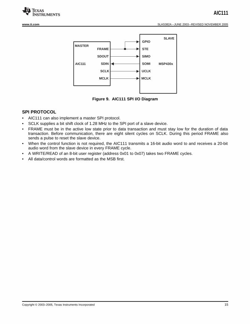
Figure 9. AIC111 SPI I/O Diagram
SPI PROTOCOL• AIC111 can also implement a master SPI protocol.• SCLK supplies a bit shift clock of 1.28 MHz to the SPI port of a slave device.• FRAME must be in the active low state prior to data transaction and must stay low for the duration of data
transaction. Before communication, there are eight silent cycles on SCLK. During this period FRAME alsosends a pulse to reset the slave device.
• When the control function is not required, the AIC111 transmits a 16-bit audio word to and receives a 20-bitaudio word from the slave device in every FRAME cycle.
• A WRITE/READ of an 8-bit user register (address 0x01 to 0x07) takes two FRAME cycles.• All data/control words are formatted as the MSB first.
Copyright © 2003–2005, Texas Instruments Incorporated 15

1718
1920
2122
2324
2526
2728
2930
3132
12
34
57
89
1011
1213
1415
166
D19
D17
D16
D15
D14
D13
D12
D11
D10
D9
D8
D7
D6
D5
D4
D3
D2
D1
D15
D14
D13
D12
D11
D10
D9
D8
D7
D6
D5
D4
D3
D2
D0
D1
A2
D0
W/R
A1
A0
3231
Don
’t C
are
D18
FR
AM
E
SC
LK
SD
IN
SD
OU
T
AIC111
SLAS382A –JUNE 2003–REVISED NOVEMBER 2005 www.ti.com
A. If A2, A1, and A0 = 0, one gets audio data only and W/R is a don't care. If in the previous frame A2, A1, and A0 = 0,then one gets both audio and control data depending on the W/R bit defined as Read = 0 and Write = 1.
Figure 10. AIC111 SPI Signals
16 Copyright © 2003–2005, Texas Instruments Incorporated
1718
1920
2122
2324
2526
2728
2930
3132
12
34
57
89
1011
1213
1415
166
D19
D17
D16
D15
D14
D13
D12
D11
D10
D9
D8
D7
D6
D5
D4
C7
C6
C5
D15
D14
D13
D12
D11
D10
D9
D8
D7
D6
D5
D4
D3
D2
D0
D1
C2
C4
C3
C1
C0
3231
Don
’t C
are
D18
FR
AM
E
SC
LK
SD
IN
SD
OU
TC
7C
6C
5C
2C
4C
3C
1C
0
AIC111
www.ti.com SLAS382A –JUNE 2003–REVISED NOVEMBER 2005
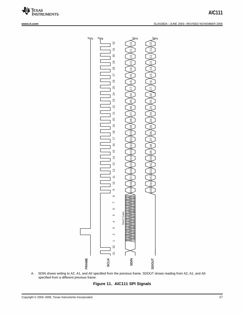
A. SDIN shows writing to A2, A1, and A0 specified from the previous frame. SDOUT shows reading from A2, A1, and A0specified from a different previous frame.
Figure 11. AIC111 SPI Signals
Copyright © 2003–2005, Texas Instruments Incorporated 17

McBSP/SPICONTROL REGISTERS
CONTROL LOGIC
DATA BLOCK
PGA/Compressor
ADC
DAC/H-Bridge
Oscillator
Power-on Reset
Mic Power/VREF
SCLK
FRAME
SDIN
SDOUT
IMODE
MCLK
AIC111
SLAS382A –JUNE 2003–REVISED NOVEMBER 2005 www.ti.com
Table 8. DIGITAL INTERFACE TIMING
PARAMETER MIN TYP MAX UNIT
F_sclk SCLK frequency 1.28 MHz
F_frame FRAME frequency F-sclk/32 MHz
Figure 12. DIGITAL INTERFACE BLOCK DIAGRAM
Table 9. REGISTER MAP AND REGISTER BIT DEFINITIONS
ADDRESS REGISTER NAME (1) DETAILED DESCRIPTION
0x00 Reserved Reserved for future use
0x01 PGACREG PGAC gain register
0x02 HPFSFTREG HPF and shift control register
0x03 PDCREG Power-down control register
0x04 FASTARREG Fast attack/release rate control register
0x05 SLOWARREG Slow attack/release rate control register
0x06-07 Reserved Reserved for future use
(1) Do not write to the reserved registers.
Table 10. PGACREG
BIT NAME FUNCTION DEFAULT=0x46
7 PGAC_READ_MODE Select register contents or actual gain to read
0: Read FORMAT0 register contents (default)
1: Read actual PGAC gain
18 Copyright © 2003–2005, Texas Instruments Incorporated

AIC111
www.ti.com SLAS382A –JUNE 2003–REVISED NOVEMBER 2005
Table 10. PGACREG (continued)
BIT NAME FUNCTION DEFAULT=0x46
6:0 PGAC_GAIN [6:0] PGAC gain adjustment (0.5 dB steps). A full table is found in theAPPENDIXof this data sheet.
0x52 = +40.0 dB
0x51 = +39.5 dB
0x50 = +39.0 dB
…
0x46 =+34.0 dB (default)
….
0x01 = -0.5 dB
0x00 = -1.0 dB
Table 11. HPFSFTREG
BIT NAME FUNCTION DEFAULT=0x11
7 DBUFF_EN Enable weak (1/2 strength) dig I/O buffer
6:5 HPF_CTL [1:0] Control bits for high-pass filter
00: normal mode
01: HPF bypass
10: 100 Hz corner frequency
11: Not used
4:2 SHIFT [2:0] Select shift bits when ADC 16-b output is used as DAC 20-b input.
000: no shift -24 db gain
001: 1b left shift -18 dB gain
010: 2b left shift -12 dB gain
011: 3b left shift -6 dB gain
100: 4b left shift (default) 0 dB gain
101: 5b left shift +6 dB gain
11X: 5b left shift
1:0 DAC_MODE Select DAC mode of operation.
00: DAC off, powered down
01: 16-bit input goes through shifter (default)
10: 20-bit input bypasses shifter
11: ADC"DAC digital loopback
Table 12. PDCREG
BIT NAME FUNCTION DEFAULT=0x00
7 DAC_ADAPTIVE_Q 0 = fixed quantization, 1 = adaptive quantization
6 HB_OUT_EN H-bridge output enable
5 HB_DRIVE H-bridge drive strength, 0 = 40Ω , 1 = 20 Ω4 HIST_TIMEOUT_SEL PGAC hysteresis timeout select
0: 50 ms (default)
1: 25 ms
3:2 PGAC_GAIN_MODE Set gain mode of PGAC
00: Automatic, dual rate (default)
01: Automatic, single rate
10: Fixed, single rate
11: Fixed, immediate
1 MIC_VSUP_PD Power down MIC_VSUP
Copyright © 2003–2005, Texas Instruments Incorporated 19
AIC111
SLAS382A –JUNE 2003–REVISED NOVEMBER 2005 www.ti.com
Table 12. PDCREG (continued)
BIT NAME FUNCTION DEFAULT=0x00
0 FRONTEND_PD Power down PGAC+ADC
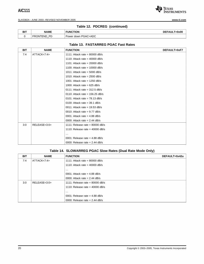
Table 13. FASTARREG PGAC Fast Rates
BIT NAME FUNCTION DEFAULT=0xF7
7:4 ATTACK<7:4> 1111: Attack rate = 80000 dB/s
1110: Attack rate = 40000 dB/s
1101: Attack rate = 20000 dB/s
1100: Attack rate = 10000 dB/s
1011: Attack rate = 5000 dB/s
1010: Attack rate = 2500 dB/s
1001: Attack rate = 1250 dB/s
1000: Attack rate = 625 dB/s
0111: Attack rate = 312.5 dB/s
0110: Attack rate = 156.25 dB/s
0101: Attack rate = 78.13 dB/s
0100: Attack rate = 39.1 dB/s
0011: Attack rate = 19.53 dB/s
0010: Attack rate = 9.77 dB/s
0001: Attack rate = 4.88 dB/s
0000: Attack rate = 2.44 dB/s
3:0 RELEASE<3:0> 1111: Release rate = 80000 dB/s
1110: Release rate = 40000 dB/s
…
0001: Release rate = 4.88 dB/s
0000: Release rate = 2.44 dB/s
Table 14. SLOWARREG PGAC Slow Rates (Dual Rate Mode Only)
BIT NAME FUNCTION DEFAULT=0x42u
7:4 ATTACK<7:4> 1111: Attack rate = 80000 dB/s
1110: Attack rate = 40000 dB/s
…
0001: Attack rate = 4.88 dB/s
0000: Attack rate = 2.44 dB/s
3:0 RELEASE<3:0> 1111: Release rate = 80000 dB/s
1110: Release rate = 40000 dB/s
…
0001: Release rate = 4.88 dB/s
0000: Release rate = 2.44 dB/s
20 Copyright © 2003–2005, Texas Instruments Incorporated
AIC111
www.ti.com SLAS382A –JUNE 2003–REVISED NOVEMBER 2005
APPENDIX
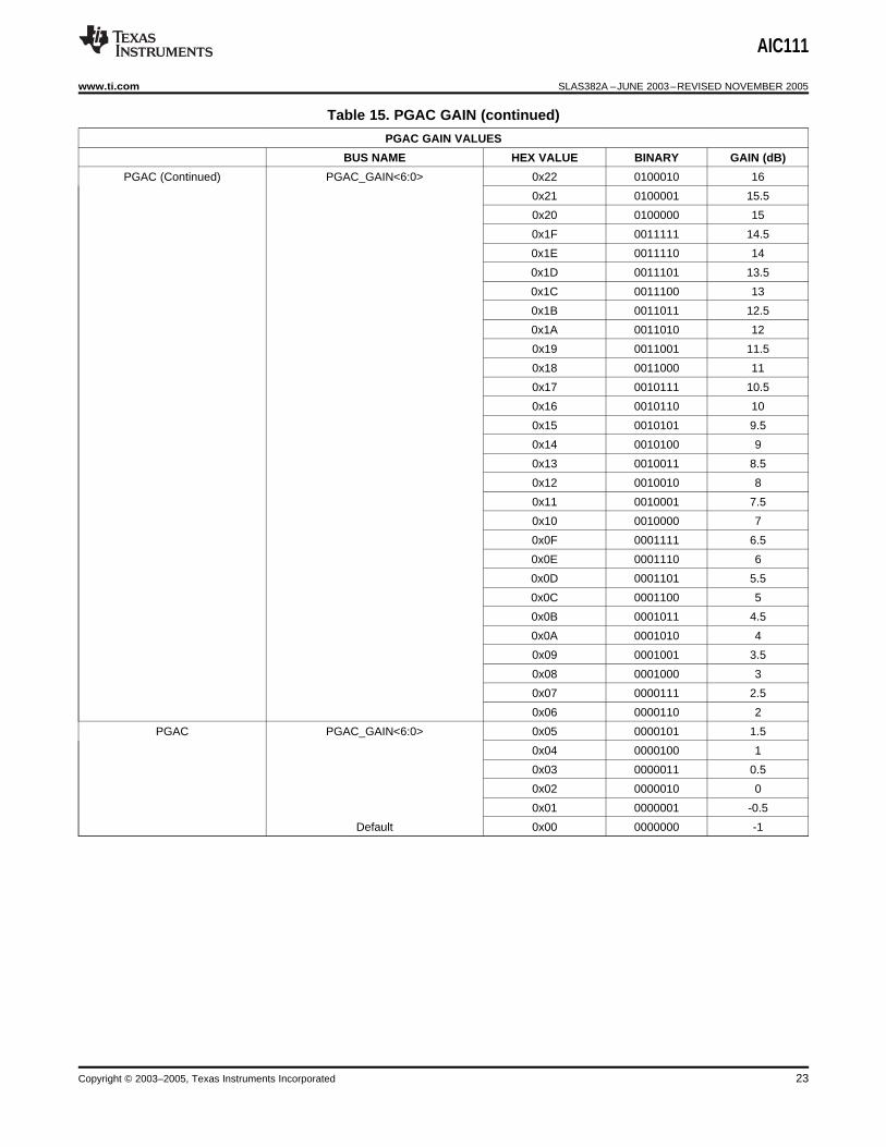
Table 15. PGAC GAIN
PGAC GAIN VALUES
BUS NAME HEX VALUE BINARY GAIN (dB)
PGAC PGAC_GAIN<6:0> 0x52 1010010 40
0x51 1010001 39.5
0x50 1010000 39
0x4F 1001111 38.5
0x4E 1001110 38
0x4D 1001101 37.5
0x4C 1001100 37
0x4B 1001011 36.5
0x4A 1001010 36
0x49 1001001 35.5
0x48 1001000 35
0x47 1000111 34.5
0x46 1000110 34
0x45 1000101 33.5
0x44 1000100 33
0x43 1000011 32.5
0x42 1000010 32
0x41 1000001 31.5
0x40 1000000 31
0x3F 0111111 30.5
0x3E 0111110 30
0x3D 0111101 29.5
0x3C 0111100 29
0x3B 0111011 28.5
0x3A 0111010 28
0x39 0111001 27.5
Copyright © 2003–2005, Texas Instruments Incorporated 21
AIC111
SLAS382A –JUNE 2003–REVISED NOVEMBER 2005 www.ti.com
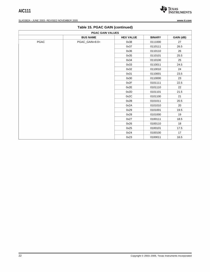
Table 15. PGAC GAIN (continued)
PGAC GAIN VALUES
BUS NAME HEX VALUE BINARY GAIN (dB)
PGAC PGAC_GAIN<6:0> 0x38 0111000 27
0x37 0110111 26.5
0x36 0110110 26
0x35 0110101 25.5
0x34 0110100 25
0x33 0110011 24.5
0x32 0110010 24
0x31 0110001 23.5
0x30 0110000 23
0x2F 0101111 22.5
0x2E 0101110 22
0x2D 0101101 21.5
0x2C 0101100 21
0x2B 0101011 20.5
0x2A 0101010 20
0x29 0101001 19.5
0x28 0101000 19
0x27 0100111 18.5
0x26 0100110 18
0x25 0100101 17.5
0x24 0100100 17
0x23 0100011 16.5
22 Copyright © 2003–2005, Texas Instruments Incorporated
AIC111
www.ti.com SLAS382A –JUNE 2003–REVISED NOVEMBER 2005
Table 15. PGAC GAIN (continued)
PGAC GAIN VALUES
BUS NAME HEX VALUE BINARY GAIN (dB)
PGAC (Continued) PGAC_GAIN<6:0> 0x22 0100010 16
0x21 0100001 15.5
0x20 0100000 15
0x1F 0011111 14.5
0x1E 0011110 14
0x1D 0011101 13.5
0x1C 0011100 13
0x1B 0011011 12.5
0x1A 0011010 12
0x19 0011001 11.5
0x18 0011000 11
0x17 0010111 10.5
0x16 0010110 10
0x15 0010101 9.5
0x14 0010100 9
0x13 0010011 8.5
0x12 0010010 8
0x11 0010001 7.5
0x10 0010000 7
0x0F 0001111 6.5
0x0E 0001110 6
0x0D 0001101 5.5
0x0C 0001100 5
0x0B 0001011 4.5
0x0A 0001010 4
0x09 0001001 3.5
0x08 0001000 3
0x07 0000111 2.5
0x06 0000110 2
PGAC PGAC_GAIN<6:0> 0x05 0000101 1.5
0x04 0000100 1
0x03 0000011 0.5
0x02 0000010 0
0x01 0000001 -0.5
Default 0x00 0000000 -1
Copyright © 2003–2005, Texas Instruments Incorporated 23

DV
DD
DV
SS
SDOUT
FRAME
SDIN
SCLK
BU
F_D
VD
DB
UF
_DV
SS
’C54x
RST/LBM
AIC111
VS
S
AV
DD
I/O
BUFFERS
VC
C
1.3V
DX
DR
RST
LBM = Low Battery Monitor
AV
SS
MCLK CLKIN
McBSP
EXT_RST/PWDN
ZINC AIRBATTERY
MIC_VSUP
Microphone
MIC_BIAS
Speaker
HB_VDD
HB_VSS
HBRIDGE
1.3V
CLKRCLKSCLKX
FSXFSR
AIC111
SLAS382A –JUNE 2003–REVISED NOVEMBER 2005 www.ti.com
TI TMS320C54xx APPLICATION CIRCUIT
Figure 13. Interfacing to the TMS320C54xx for a Hearing Aid Application
Required external capacitors:• 1-μF coupling capacitor on AVINP, AVINM• 1-μF from VMID_FILT to analog ground• 1-μF from VREF to analog ground• 0.1-μF from MIC_VSUP to analog ground• At least 0.1-μF from VRFILT to analog ground. 1-μF from VRFILT to analog ground is recommended.
24 Copyright © 2003–2005, Texas Instruments Incorporated
DV
DD
MIC_VSUP
DV
SS
Speaker
SDOUT
FRAME
SDIN
SCLK
BU
F_D
VD
DB
UF
_DV
SS
MSP430F12x
RST/LBM
AIC111
VS
S
AV
DD
I/O
BUFFERS
Microphone
2.8 V
1.3 V
SOMI
INCLK
SIMO
STE
MIC_BIAS
AV
SS
MCLK XIN
RST/NMI
VC
C
P2.5(See Note A)
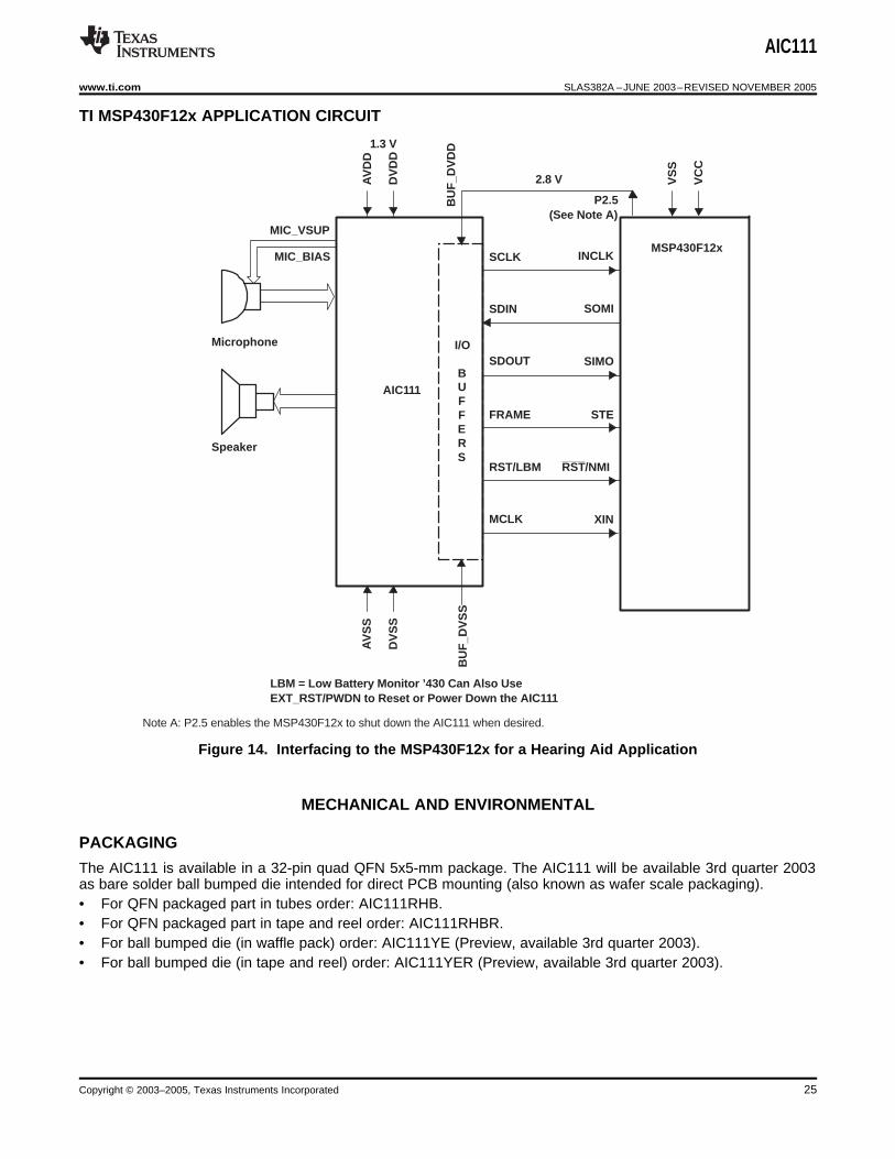
Note A: P2.5 enables the MSP430F12x to shut down the AIC111 when desired.
LBM = Low Battery Monitor ’430 Can Also UseEXT_RST/PWDN to Reset or Power Down the AIC111
AIC111
www.ti.com SLAS382A –JUNE 2003–REVISED NOVEMBER 2005
TI MSP430F12x APPLICATION CIRCUIT
Figure 14. Interfacing to the MSP430F12x for a Hearing Aid Application
MECHANICAL AND ENVIRONMENTAL
PACKAGING
The AIC111 is available in a 32-pin quad QFN 5x5-mm package. The AIC111 will be available 3rd quarter 2003as bare solder ball bumped die intended for direct PCB mounting (also known as wafer scale packaging).• For QFN packaged part in tubes order: AIC111RHB.• For QFN packaged part in tape and reel order: AIC111RHBR.• For ball bumped die (in waffle pack) order: AIC111YE (Preview, available 3rd quarter 2003).• For ball bumped die (in tape and reel) order: AIC111YER (Preview, available 3rd quarter 2003).
Copyright © 2003–2005, Texas Instruments Incorporated 25

AIC111
SLAS382A –JUNE 2003–REVISED NOVEMBER 2005 www.ti.com
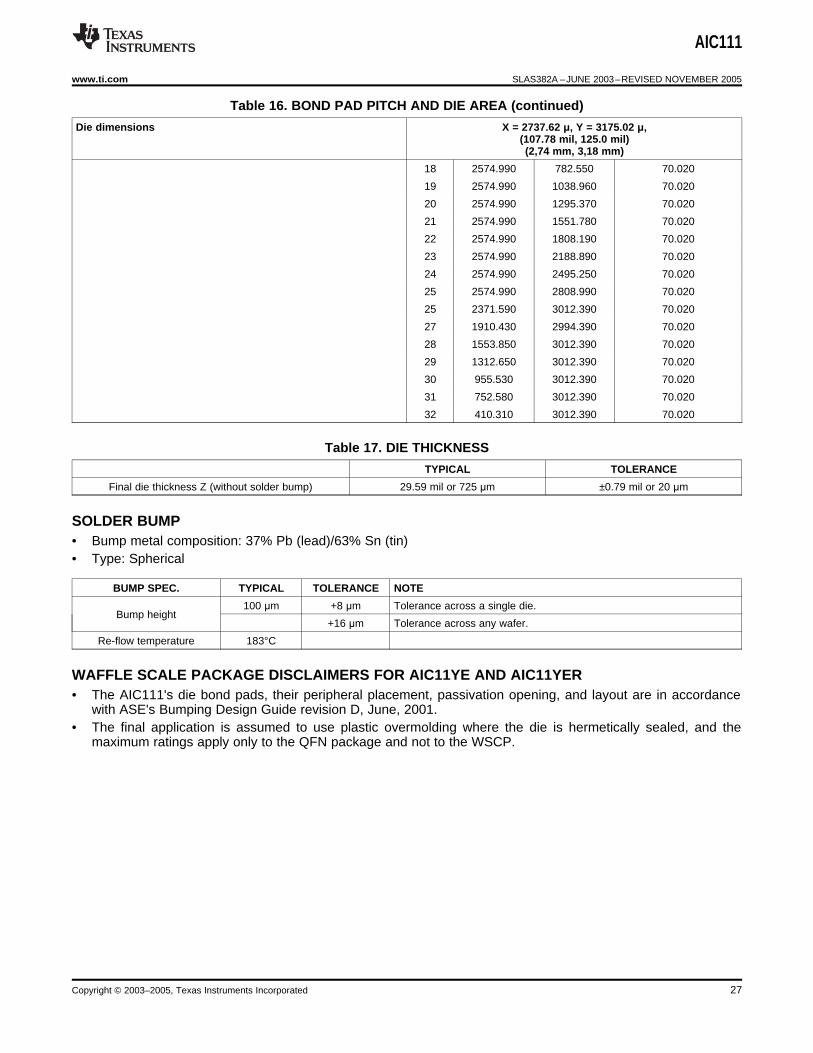
Table 16. BOND PAD PITCH AND DIE AREA
Die dimensions X = 2737.62 μ, Y = 3175.02 μ,(107.78 mil, 125.0 mil)(2,74 mm, 3,18 mm)
Maximum die area (includes scribe area) 13.47kmil2 (8.69mm2)
Minimum bond pad pitch 202.95 μ or 7.99 mil
Nearest PITCH
PAD (#) PAD (#) (micron) (mil)
7 8 202.950 (7.990)
30 31 202.950 (7.990)
12 13 237.690 (9.358)
14 15 237.690 (9.358)
16 15 237.690 (9.358)
28 29 241.200 (9.496)
18 19 256.410 (10.095)
20 19 256.410 (10.095)
21 20 256.410 (10.095)
22 21 256.410 (10.095)
25 26 287.651 (11.325)
9 10 295.470 (11.633)
10 11 295.470 (11.633)
23 24 306.360 (12.061)
1 32 327.147 (12.880)
32 1 327.147 (12.880)
4 5 356.940 (14.053)
27 28 357.034 (14.056)
17 16 359.453 (14.152)
6 7 369.450 (14.545)
2 1 371.520 (14.627)
3 2 380.700 (14.988)
Number of pins 32
Pad locations: Bond Pad Coordinates Bond Pad Dimensions
Units: microns Pad # Xcenter Ycenter Diameter
Dimensions: X = 2737.62 Y = 3175 1 154.080 2808.990 70.020
Bond pad origin: X = 0.000 Y = 0.000 2 154.080 2437.470 70.020
Bond pad offset: X = 0.000 Y = 0.000 3 154.080 2056.770 70.020
(X,Y) = (0,0) is located at the left bottom of the die by pads 8 and 9. 4 154.080 1676.070 70.020
See Figure 1. 5 154.080 1319.130 70.020
6 154.080 938.430 70.020
7 154.080 568.980 70.020
8 154.080 366.030 70.020
9 410.310 162.630 70.020
10 705.780 162.630 70.020
11 1001.250 162.630 70.020
12 1327.860 162.630 70.020
13 1565.550 162.630 70.020
14 1803.240 162.630 70.020
15 2040.930 162.630 70.020
16 2278.620 162.630 70.020
17 2574.990 366.030 70.020
26 Copyright © 2003–2005, Texas Instruments Incorporated
AIC111
www.ti.com SLAS382A –JUNE 2003–REVISED NOVEMBER 2005
Table 16. BOND PAD PITCH AND DIE AREA (continued)
Die dimensions X = 2737.62 μ, Y = 3175.02 μ,(107.78 mil, 125.0 mil)(2,74 mm, 3,18 mm)
18 2574.990 782.550 70.020
19 2574.990 1038.960 70.020
20 2574.990 1295.370 70.020
21 2574.990 1551.780 70.020
22 2574.990 1808.190 70.020
23 2574.990 2188.890 70.020
24 2574.990 2495.250 70.020
25 2574.990 2808.990 70.020
25 2371.590 3012.390 70.020
27 1910.430 2994.390 70.020
28 1553.850 3012.390 70.020
29 1312.650 3012.390 70.020
30 955.530 3012.390 70.020
31 752.580 3012.390 70.020
32 410.310 3012.390 70.020
Table 17. DIE THICKNESS
TYPICAL TOLERANCE
Final die thickness Z (without solder bump) 29.59 mil or 725 μm ±0.79 mil or 20 μm
SOLDER BUMP• Bump metal composition: 37% Pb (lead)/63% Sn (tin)• Type: Spherical
BUMP SPEC. TYPICAL TOLERANCE NOTE
100 μm +8 μm Tolerance across a single die.Bump height
+16 μm Tolerance across any wafer.
Re-flow temperature 183°C
WAFFLE SCALE PACKAGE DISCLAIMERS FOR AIC11YE AND AIC11YER• The AIC111's die bond pads, their peripheral placement, passivation opening, and layout are in accordance
with ASE's Bumping Design Guide revision D, June, 2001.• The final application is assumed to use plastic overmolding where the die is hermetically sealed, and the
maximum ratings apply only to the QFN package and not to the WSCP.
Copyright © 2003–2005, Texas Instruments Incorporated 27
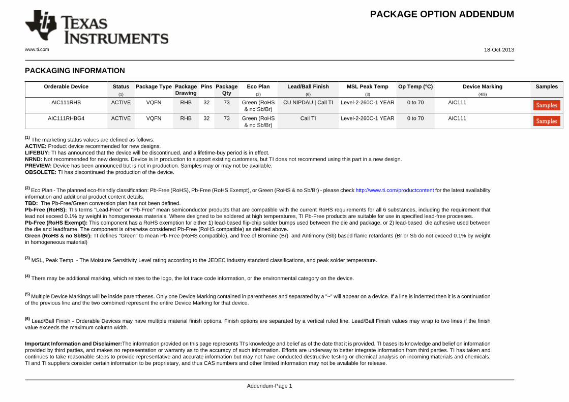
PACKAGE OPTION ADDENDUM
www.ti.com 18-Oct-2013
Addendum-Page 1
PACKAGING INFORMATION
Orderable Device Status(1)
Package Type PackageDrawing
Pins PackageQty
Eco Plan(2)
Lead/Ball Finish(6)
MSL Peak Temp(3)
Op Temp (°C) Device Marking(4/5)
Samples
AIC111RHB ACTIVE VQFN RHB 32 73 Green (RoHS& no Sb/Br)
CU NIPDAU | Call TI Level-2-260C-1 YEAR 0 to 70 AIC111
AIC111RHBG4 ACTIVE VQFN RHB 32 73 Green (RoHS& no Sb/Br)
Call TI Level-2-260C-1 YEAR 0 to 70 AIC111
(1) The marketing status values are defined as follows:ACTIVE: Product device recommended for new designs.LIFEBUY: TI has announced that the device will be discontinued, and a lifetime-buy period is in effect.NRND: Not recommended for new designs. Device is in production to support existing customers, but TI does not recommend using this part in a new design.PREVIEW: Device has been announced but is not in production. Samples may or may not be available.OBSOLETE: TI has discontinued the production of the device.
(2) Eco Plan - The planned eco-friendly classification: Pb-Free (RoHS), Pb-Free (RoHS Exempt), or Green (RoHS & no Sb/Br) - please check http://www.ti.com/productcontent for the latest availabilityinformation and additional product content details.TBD: The Pb-Free/Green conversion plan has not been defined.Pb-Free (RoHS): TI's terms "Lead-Free" or "Pb-Free" mean semiconductor products that are compatible with the current RoHS requirements for all 6 substances, including the requirement thatlead not exceed 0.1% by weight in homogeneous materials. Where designed to be soldered at high temperatures, TI Pb-Free products are suitable for use in specified lead-free processes.Pb-Free (RoHS Exempt): This component has a RoHS exemption for either 1) lead-based flip-chip solder bumps used between the die and package, or 2) lead-based die adhesive used betweenthe die and leadframe. The component is otherwise considered Pb-Free (RoHS compatible) as defined above.Green (RoHS & no Sb/Br): TI defines "Green" to mean Pb-Free (RoHS compatible), and free of Bromine (Br) and Antimony (Sb) based flame retardants (Br or Sb do not exceed 0.1% by weightin homogeneous material)
(3) MSL, Peak Temp. - The Moisture Sensitivity Level rating according to the JEDEC industry standard classifications, and peak solder temperature.
(4) There may be additional marking, which relates to the logo, the lot trace code information, or the environmental category on the device.
(5) Multiple Device Markings will be inside parentheses. Only one Device Marking contained in parentheses and separated by a "~" will appear on a device. If a line is indented then it is a continuationof the previous line and the two combined represent the entire Device Marking for that device.
(6) Lead/Ball Finish - Orderable Devices may have multiple material finish options. Finish options are separated by a vertical ruled line. Lead/Ball Finish values may wrap to two lines if the finishvalue exceeds the maximum column width.
Important Information and Disclaimer:The information provided on this page represents TI's knowledge and belief as of the date that it is provided. TI bases its knowledge and belief on informationprovided by third parties, and makes no representation or warranty as to the accuracy of such information. Efforts are underway to better integrate information from third parties. TI has taken andcontinues to take reasonable steps to provide representative and accurate information but may not have conducted destructive testing or chemical analysis on incoming materials and chemicals.TI and TI suppliers consider certain information to be proprietary, and thus CAS numbers and other limited information may not be available for release.

PACKAGE OPTION ADDENDUM
www.ti.com 18-Oct-2013
Addendum-Page 2
In no event shall TI's liability arising out of such information exceed the total purchase price of the TI part(s) at issue in this document sold by TI to Customer on an annual basis.
IMPORTANT NOTICE
Texas Instruments Incorporated and its subsidiaries (TI) reserve the right to make corrections, enhancements, improvements and otherchanges to its semiconductor products and services per JESD46, latest issue, and to discontinue any product or service per JESD48, latestissue. Buyers should obtain the latest relevant information before placing orders and should verify that such information is current andcomplete. All semiconductor products (also referred to herein as “components”) are sold subject to TI’s terms and conditions of salesupplied at the time of order acknowledgment.TI warrants performance of its components to the specifications applicable at the time of sale, in accordance with the warranty in TI’s termsand conditions of sale of semiconductor products. Testing and other quality control techniques are used to the extent TI deems necessaryto support this warranty. Except where mandated by applicable law, testing of all parameters of each component is not necessarilyperformed.TI assumes no liability for applications assistance or the design of Buyers’ products. Buyers are responsible for their products andapplications using TI components. To minimize the risks associated with Buyers’ products and applications, Buyers should provideadequate design and operating safeguards.TI does not warrant or represent that any license, either express or implied, is granted under any patent right, copyright, mask work right, orother intellectual property right relating to any combination, machine, or process in which TI components or services are used. Informationpublished by TI regarding third-party products or services does not constitute a license to use such products or services or a warranty orendorsement thereof. Use of such information may require a license from a third party under the patents or other intellectual property of thethird party, or a license from TI under the patents or other intellectual property of TI.Reproduction of significant portions of TI information in TI data books or data sheets is permissible only if reproduction is without alterationand is accompanied by all associated warranties, conditions, limitations, and notices. TI is not responsible or liable for such altereddocumentation. Information of third parties may be subject to additional restrictions.Resale of TI components or services with statements different from or beyond the parameters stated by TI for that component or servicevoids all express and any implied warranties for the associated TI component or service and is an unfair and deceptive business practice.TI is not responsible or liable for any such statements.Buyer acknowledges and agrees that it is solely responsible for compliance with all legal, regulatory and safety-related requirementsconcerning its products, and any use of TI components in its applications, notwithstanding any applications-related information or supportthat may be provided by TI. Buyer represents and agrees that it has all the necessary expertise to create and implement safeguards whichanticipate dangerous consequences of failures, monitor failures and their consequences, lessen the likelihood of failures that might causeharm and take appropriate remedial actions. Buyer will fully indemnify TI and its representatives against any damages arising out of the useof any TI components in safety-critical applications.In some cases, TI components may be promoted specifically to facilitate safety-related applications. With such components, TI’s goal is tohelp enable customers to design and create their own end-product solutions that meet applicable functional safety standards andrequirements. Nonetheless, such components are subject to these terms.No TI components are authorized for use in FDA Class III (or similar life-critical medical equipment) unless authorized officers of the partieshave executed a special agreement specifically governing such use.Only those TI components which TI has specifically designated as military grade or “enhanced plastic” are designed and intended for use inmilitary/aerospace applications or environments. Buyer acknowledges and agrees that any military or aerospace use of TI componentswhich have not been so designated is solely at the Buyer's risk, and that Buyer is solely responsible for compliance with all legal andregulatory requirements in connection with such use.TI has specifically designated certain components as meeting ISO/TS16949 requirements, mainly for automotive use. In any case of use ofnon-designated products, TI will not be responsible for any failure to meet ISO/TS16949.
Products ApplicationsAudio www.ti.com/audio Automotive and Transportation www.ti.com/automotiveAmplifiers amplifier.ti.com Communications and Telecom www.ti.com/communicationsData Converters dataconverter.ti.com Computers and Peripherals www.ti.com/computersDLP® Products www.dlp.com Consumer Electronics www.ti.com/consumer-appsDSP dsp.ti.com Energy and Lighting www.ti.com/energyClocks and Timers www.ti.com/clocks Industrial www.ti.com/industrialInterface interface.ti.com Medical www.ti.com/medicalLogic logic.ti.com Security www.ti.com/securityPower Mgmt power.ti.com Space, Avionics and Defense www.ti.com/space-avionics-defenseMicrocontrollers microcontroller.ti.com Video and Imaging www.ti.com/videoRFID www.ti-rfid.comOMAP Applications Processors www.ti.com/omap TI E2E Community e2e.ti.comWireless Connectivity www.ti.com/wirelessconnectivity
Mailing Address: Texas Instruments, Post Office Box 655303, Dallas, Texas 75265Copyright © 2016, Texas Instruments Incorporated