agilent e4438c esg vector signal generator -...
TRANSCRIPT

Agilent E4438C ESG Vector Signal GeneratorData Sheet
Migrate to the new Agilent MXG X-Series signal generator and generate true performance
The new MXG exceeds the ESG's performance in every category - output power, ACPR, EVM, phase noise, bandwidth and memory depth - and offers a wider range of signal simulation, with both real-time and arbitrary
waveform generation capabilities. For more information, visit www.agilent.com/find/X-Series_SG
2
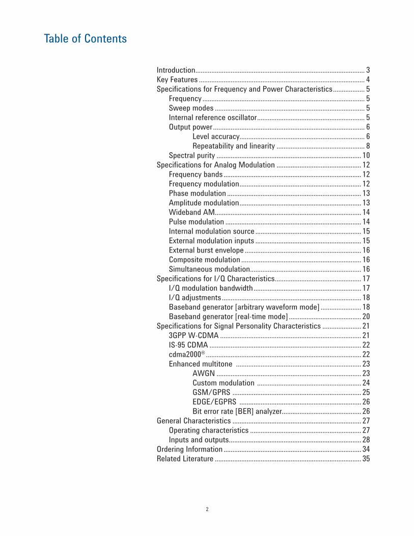
Introduction ................................................................................................ 3Key Features .............................................................................................. 4Specifications for Frequency and Power Characteristics .................. 5 Frequency ............................................................................................ 5 Sweep modes ..................................................................................... 5 Internal reference oscillator ............................................................. 5 Output power ...................................................................................... 6 Level accuracy....................................................................... 6 Repeatability and linearity .................................................. 8 Spectral purity .................................................................................. 10Specifications for Analog Modulation ................................................ 12 Frequency bands .............................................................................. 12 Frequency modulation ..................................................................... 12 Phase modulation ............................................................................ 13 Amplitude modulation ..................................................................... 13 Wideband AM ................................................................................... 14 Pulse modulation ............................................................................. 14 Internal modulation source ............................................................ 15 External modulation inputs ............................................................ 15 External burst envelope .................................................................. 16 Composite modulation .................................................................... 16 Simultaneous modulation ............................................................... 16Specifications for I/Q Characteristics ................................................. 17 I/Q modulation bandwidth ............................................................. 17 I/Q adjustments ............................................................................... 18 Baseband generator [arbitrary waveform mode] ....................... 18 Baseband generator [real-time mode] ......................................... 20Specifications for Signal Personality Characteristics ...................... 21 3GPP W-CDMA ................................................................................ 21 IS-95 CDMA ...................................................................................... 22 cdma2000® ........................................................................................ 22 Enhanced multitone ....................................................................... 23 AWGN .................................................................................. 23 Custom modulation ........................................................... 24 GSM/GPRS ......................................................................... 25 EDGE/EGPRS ..................................................................... 26 Bit error rate [BER] analyzer............................................. 26General Characteristics ......................................................................... 27 Operating characteristics ............................................................... 27 Inputs and outputs ........................................................................... 28Ordering Information .............................................................................. 34Related Literature ................................................................................... 35
Table of Contents
3
Introduction
E4438C ESGvector signal generator
Definitions
Agilent Technologies E4438C ESG vector signal generator incorporates a broad array of capabilities for testing both analog and digital communications systems. Flexible options provide test solutions that will evaluate the performance of nearly all current and proposed air interface standards. Many test functions can be customized to meet the needs of proprietary and other nonstandard wireless protocols as well. You can configure your instrument to address a wide variety of tests—from altering nearly every aspect of a digital signal or signal operating environment, to creating experimental signals. This flexibility, along with an architecture that accepts future enhancements makes the E4438C ESG vector signal generator an excellent choice for wireless communications system testing now and in the future.
Choose your required frequency range as an Option when configuring your E4438C ESG vector signal generator. Please refer to the E4438C Configuration Guide for complete ordering information. Literature number 5988-4085EN.
Specifications (spec): Specifications describe the instrument’s warranted performance and apply after a 45 minute warm-up. All specifications are valid over the signal generators entire operating/environmental range unless otherwise noted. Supplemental characteristics, denoted typical or nominal, provide additional [nonwarranted] information useful in applying the instrument. Column headings labeled “standard” imply that this level of performance is standard, without regard for option configuration. If a particular option configuration modifies the standard performance, that performance is given in a separate column.
Typical (typ): performance is not warranted. It applies at 25°C. 80% of all products meet typical performance.
Nominal (nom): values are not warranted. They represent the value of a parameter that is most likely to occur; the expected or mean value. They are included to facilitate the application of the product.
Standard (std): No options are included when referring to the signal generator unless noted otherwise.
4
Key Features
Key standard features
Optional features
• Expandable architecture
• Broad frequency coverage
• High-stability time-base
• Choice of electronic or mechanical attenuator
• Superior level accuracy
• Wideband FM and FM
• Step and list sweep, both frequency and power
• Built-in function generator
• Lightweight, rack-mountable
• 1-year standard warranty
• 2-year calibration cycle
• Broadband analog I/Q inputs
• I/Q adjustment capabilities and internal calibration routine
• Excellent modulation accuracy and stability
• Coherent carrier output up to 4 GHz
• Internal baseband generator, 8 or 64 MSa (40 or 320 MB) memory with digital bus capability
• ESG digital input or output connectivity with N5102A Baseband Studio digital signal interface module
• 6 GB internal hard drive
• Internal bit error rate (BER) analyzer
• Enhanced phase noise performance
• High output power with mechanical attenuator
• Move all front panel connectors to the rear panel
• Real-time channel emulation, up to 4x2 MIMO, with the N5106A PXB MIMO receiver tester
• Signal Creation software – Signal Studio software – Embedded software – A complete list of software can be found in the ordering information section or at www.agilent.com/find/signalstudio
This document contains the measured specifications for the instrument platform and personalities. It does not contain a full list of features for all optional personalities. Please consult the individual product overviews for each personality for a full listing of all features and capabilities. These are listed at the end of this document.
5
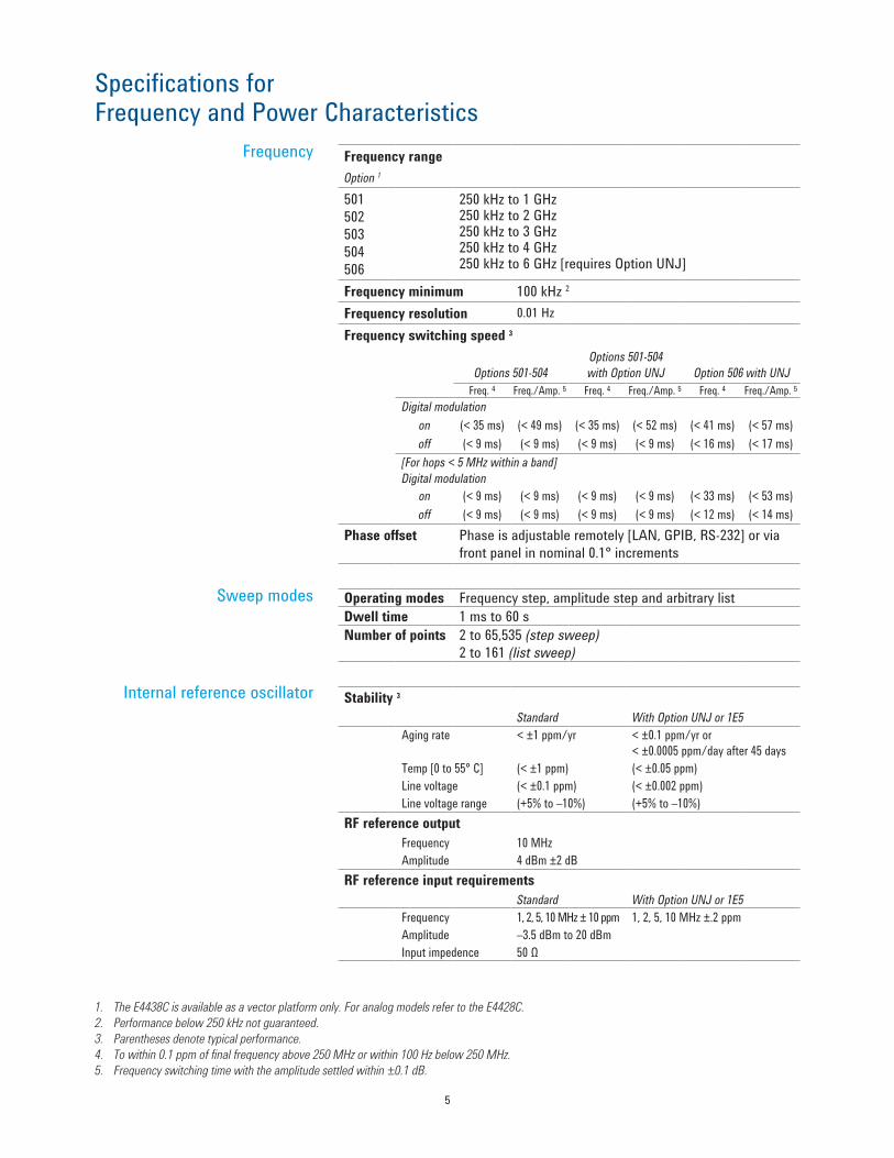
Specifications for Frequency and Power Characteristics
Frequency
Sweep modes
Internal reference oscillator
Frequency rangeOption 1
501502503504506
250 kHz to 1 GHz250 kHz to 2 GHz250 kHz to 3 GHz250 kHz to 4 GHz250 kHz to 6 GHz [requires Option UNJ]
Frequency minimum 100 kHz 2
Frequency resolution 0.01 HzFrequency switching speed 3
Options 501-504Options 501-504 with Option UNJ Option 506 with UNJ
Freq. 4 Freq./Amp. 5 Freq. 4 Freq./Amp. 5 Freq. 4 Freq./Amp. 5Digital modulation
on (< 35 ms) (< 49 ms) (< 35 ms) (< 52 ms) (< 41 ms) (< 57 ms)off (< 9 ms) (< 9 ms) (< 9 ms) (< 9 ms) (< 16 ms) (< 17 ms)
[For hops < 5 MHz within a band]Digital modulation
on (< 9 ms) (< 9 ms) (< 9 ms) (< 9 ms) (< 33 ms) (< 53 ms)off (< 9 ms) (< 9 ms) (< 9 ms) (< 9 ms) (< 12 ms) (< 14 ms)
Phase offset Phase is adjustable remotely [LAN, GPIB, RS-232] or via front panel in nominal 0.1° increments
Operating modes Frequency step, amplitude step and arbitrary listDwell time 1 ms to 60 sNumber of points 2 to 65,535 (step sweep)
2 to 161 (list sweep)
Stability 3
Standard With Option UNJ or 1E5Aging rate < ±1 ppm/yr < ±0.1 ppm/yr or
< ±0.0005 ppm/day after 45 daysTemp [0 to 55° C] (< ±1 ppm) (< ±0.05 ppm)Line voltage (< ±0.1 ppm) (< ±0.002 ppm)Line voltage range (+5% to –10%) (+5% to –10%)
RF reference outputFrequency 10 MHzAmplitude 4 dBm ±2 dB
RF reference input requirementsStandard With Option UNJ or 1E5
Frequency 1, 2, 5, 10 MHz ± 10 ppm 1, 2, 5, 10 MHz ±.2 ppmAmplitude –3.5 dBm to 20 dBmInput impedence 50 Ω
1. The E4438C is available as a vector platform only. For analog models refer to the E4428C.2. Performance below 250 kHz not guaranteed.3. Parentheses denote typical performance.4. To within 0.1 ppm of final frequency above 250 MHz or within 100 Hz below 250 MHz.5. Frequency switching time with the amplitude settled within ±0.1 dB.

6
Specifications for Frequency and Power Characteristics
Output power PowerOptions 501-504 With Option UNB Option 506
250 kHz to 250 MHz> 250 MHz to 1 GHz> 1 to 3 GHz> 3 to 4 GHz> 4 to 6 GHz
+11 to –136 dBm+13 to –136 dBm+10 to –136 dBm+7 to –136 dBmN/A
+15 to –136 dBm+17 to –136 dBm+16 to –136 dBm+13 to –136 dBmN/A
+12 to –136 dBm+14 to –136 dBm+13 to –136 dBm+10 to –136 dBm+10 to –136 dBm
Typical maximum available power
Level resolution 0.02 dBLevel range with Attenuator Hold active
Options 501-504 with Option UNB Option 506250 kHz to 1 GHz> 1 to 3 GHz> 3 to 4 GHz> 4 to 6 GHz
23 dB20 dB17 dBN/A
27 dB26 dB23 dBN/A
24 dB23 dB20 dB20 dB
Level accuracy [dB]Options 501-504 1, 2
Power level+7 to–50 dBm
< –50 to–110 dBm
< –110 to–127 dBm
< –127 dBm
250 kHz to 2.0 GHz ±0.5 ±0.5 ±0.7 (±1.5)2.0 to 3 GHz ±0.6 ±0.6 ±0.8 (±2.5)3 to 4 GHz ±0.7 ±0.7 ±0.9 (±2.5)
With Option UNB 2, 3
Power level+10 to–50 dBm
< –50 to–110 dBm
< –110 to–127 dBm
< –127 dBm
250 kHz to 2.0 GHz ±0.5 ±0.7 ±0.8 (±1.5)> 2.0 to 3 GHz ±0.6 ±0.8 ±1.0 (±2.5)> 3 to 4 GHz ±0.8 ±0.9 ±1.3 (±2.5)
Option 506 2, 4
Power level+7 to–50 dBm
< –50 to–110 dBm
< –110 to–127 dBm
< –127 dBm
250 kHz to 2.0 GHz ±0.6 ±0.8 ±0.8 (±1.5)> 2.0 to 3 GHz ±0.6 ±0.8 ±1.0 (±2.5)> 3 to 4 GHz ±0.8 ±0.9 ±1.5 (±2.5)> 4 to 6 GHz ±0.8 ±0.9 (±1.5)
1. Quoted specifications for 23 °C ± 5 °C. Accuracy degrades by less than 0.03 dB/°C over full temperature range. Accuracy degrades by 0.3 dB above +7 dBm, and by 0.8 dB above +10 dBm.
2. Parentheses denote typical performance.3. Quoted specifications for 23 °C ± 5 °C.
Accuracy degrades by less than 0.03 dB/°C over full temperature range. Accuracy degrades by 0.2 dB above +10 dBm, and by 0.8 dB above +13 dBm.
4. Quoted specifications for 23 °C ± 5 °C. Accuracy degrades by less than 0.02 dB/°C over full temperature range. Accuracy degrades by 0.2 dB above +7 dBm.
Pow
er [d
Bm]
3000
26
24
22
20
18
16
14
12
10
Frequency [MHz]
4000
Option 501-504
5000 60000 1000 2000
Option 506Option UNB
7
Specifications for Frequency and Power Characteristics
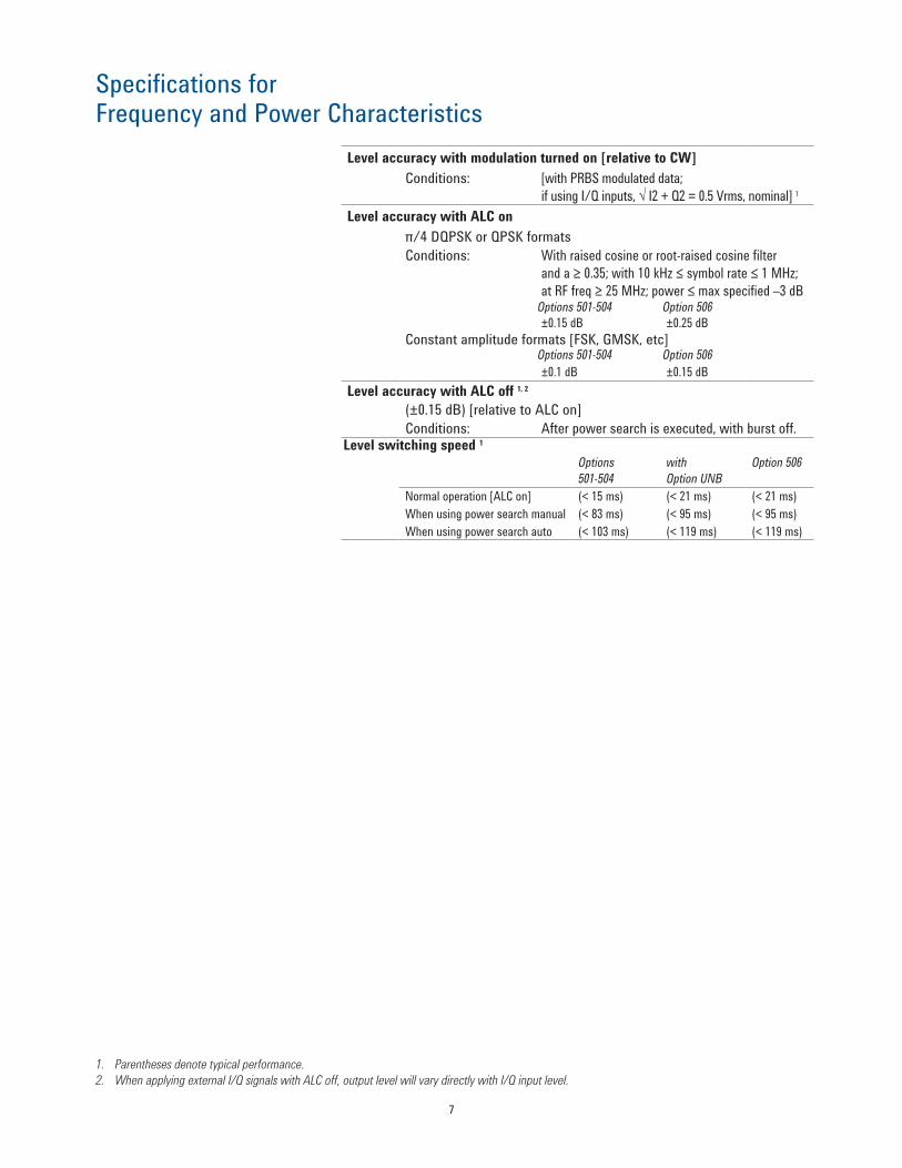
Level accuracy with modulation turned on [relative to CW]Conditions: [with PRBS modulated data;
if using I/Q inputs, √ I2 + Q2 = 0.5 Vrms, nominal] 1
Level accuracy with ALC onπ/4 DQPSK or QPSK formatsConditions: With raised cosine or root-raised cosine filter
and a ≥ 0.35; with 10 kHz ≤ symbol rate ≤ 1 MHz; at RF freq ≥ 25 MHz; power ≤ max specified –3 dB
Options 501-504 Option 506±0.15 dB ±0.25 dB
Constant amplitude formats [FSK, GMSK, etc]Options 501-504 Option 506±0.1 dB ±0.15 dB
Level accuracy with ALC off 1, 2
(±0.15 dB) [relative to ALC on]Conditions: After power search is executed, with burst off.
Level switching speed 1
Options 501-504
with Option UNB
Option 506
Normal operation [ALC on] (< 15 ms) (< 21 ms) (< 21 ms)When using power search manual (< 83 ms) (< 95 ms) (< 95 ms)When using power search auto (< 103 ms) (< 119 ms) (< 119 ms)
1. Parentheses denote typical performance.2. When applying external I/Q signals with ALC off, output level will vary directly with I/Q input level.
8
Specifications for Frequency and Power Characteristics
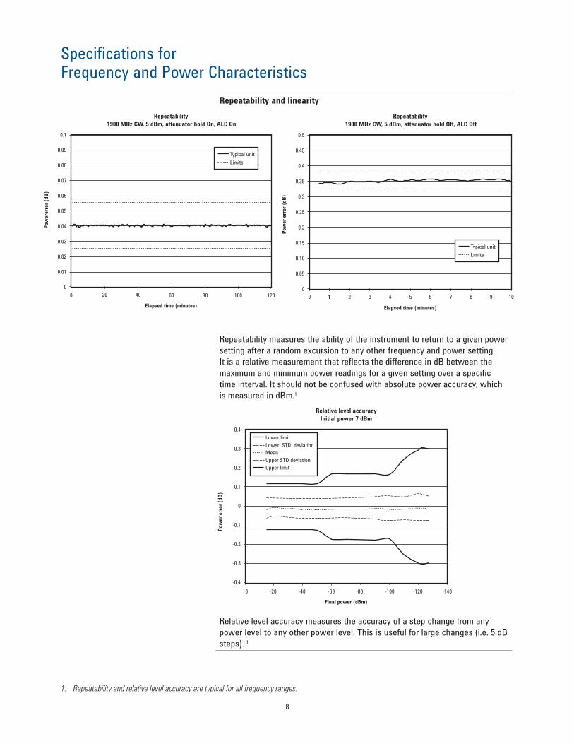
Repeatability and linearity
Repeatability measures the ability of the instrument to return to a given power setting after a random excursion to any other frequency and power setting. It is a relative measurement that reflects the difference in dB between the maximum and minimum power readings for a given setting over a specific time interval. It should not be confused with absolute power accuracy, which is measured in dBm.1
Relative level accuracy measures the accuracy of a step change from any power level to any other power level. This is useful for large changes (i.e. 5 dB steps). 1
Repeatability1900 MHz CW, 5 dBm, attenuator hold On, ALC On
0 20 40 60 80 100 120
Elapsed time (minutes)
Pow
erer
ror (
dB)
0.1
0.09
0.08
0.07
0.06
0.05
0.04
0.03
0.02
0.01
0
Typical unitLimits
Repeatability1900 MHz CW, 5 dBm, attenuator hold Off, ALC Off
0 1
Elapsed time (minutes)
Pow
er e
rror (
dB)
0.5
0.45
0.4
0.35
0.3
0.25
0.2
0.15
0.10
0.05
02 3 54 6 71 8 9 10
Typical unitLimits
1. Repeatability and relative level accuracy are typical for all frequency ranges.
Relative level accuracyInitial power 7 dBm
0 -20 -40 -60
Final power (dBm)
Pow
er e
rror (
dB)
0.4
0.3
0.2
0.1
0
-0.1
-0.2
-0.3
-0.4-140-120-80 -100
Lower limitLower STD deviationMeanUpper STD deviationUpper limit

9
Specifications for Frequency and Power Characteristics
1. Repeatability and relative level accuracy are typical for all frequency ranges.
Linearity measures the accuracy of small changes while the attenuator is held in a steady state (to avoid power glitches). This is useful for fine resolution changes. 1
LinearityCW or GSM, 850 MHz, attenuator hold On, ALC On
-10 -8 -6 -4 -2 0 8 12
Amplitude (dBm)
ALC
offs
et e
rror (
dB)
0.3
0.25
0.2
0.15
0.1
0.05
0
-0.05
-0.1
-0.15
-0.2
-0.25
-0.3
-0.35
-0.414102 4 6
Typical STD unitTypical Option UNB unitTypical Option 506 unitLower limitUpper limit
16
Limit is undefined above 13 dBMfor STD units. Limit line applies only to UNB and 506 units.
LinearityCW or GSM, 1900 MHz, attenuator hold On, ALC On
-10 -8 -6 -4 -2 0 8 12
Amplitude (dBm)
ALC
offs
et e
rror (
dB)
0.3
0.25
0.2
0.15
0.1
0.05
0
-0.05
-0.1
-0.15
-0.2
-0.25
-0.314 16102 4 6
Typical STD unitTypical Option 506 unitTypical Option UNB unitLower limitUpper limit
LinearityW-CDMA 2200 MHz, attenuator hold On, ALC On
-10 -8 -6 -4 -2 0 2 4
Amplitude (dBm)
ALC
offs
et e
rror (
dB)
0.3
0.25
0.2
0.15
0.1
0.05
0
-0.05
-0.1
-0.15
-0.2
-0.25
-0.36 8
Typical STD unitTypical Option UNB unitTypical Option 506 unitLower limitUpper limit
LinearityCW or GSM 5750 MHz, attenuator hold On, ALC On
-10 -8
Amplitude (dBm)
ALC
offs
et e
rror (
dB)
0.3
0.25
0.2
0.15
0.1
0.05
0
-0.05
-0.1
-0.15
-0.2
-0.25
-0.3-6 -4 -2 0 2 4 6 8 10
Typical STD unitLower STD deviationUpper STD deviation
Lower limitUpper limit
LinearityW-CDMA 5750 MHz, attenuator hold On, ALC On
-10 -8 -6 -4 -2 0 2 4 6 8
Amplitude (dBm)
ALC
Offs
et e
rror (
dB)
0.3
0.25
0.2
0.15
0.1
0.05
0
-0.05
-0.1
-0.15
-0.2
-0.25
-0.3
Mean,Option 506 unitLower STD deviationUpper STD deviationLower limitUpper limit

10
Specifications for Frequency and Power Characteristics
1. Parentheses denote typical performance.2. Refer to frequency bands on page 12 for
N values.3. Harmonic performance outside the operat-
ing range of the instrument is typical.4. Spurs outside the operating range of the
instrument are not specified. Broadband noise is not tested.
5. Specifications apply for FM deviations < 100 kHz and are not valid on FM. For non-constant amplitude formats, unspecified spur levels occur up to the second harmonic of the baseband rate.
6. Specifications apply for CW mode only.7. Calculated from phase noise performance
in CW mode only at -2.5 dBm for standard instruments, -0.5 dBm with Option 506, and +2.5 dBm with Option UNB.
8. For other frequencies, data rates, or bandwidths, please contact your sales representative.
SSB CW Phase noise [at 20 kHz offset] 1
Standard With Option UNJat 500 MHzat 1 GHzat 2 GHzat 3 GHzat 4 GHzat 6 GHz
(< –124 dBc/Hz)(< –118 dBc/Hz)(< –112 dBc/Hz)(< –106 dBc/Hz)(< –106 dBc/Hz)
N/A
< –135 dBc/Hz, (< –138 dBc/Hz)< –130 dBc/Hz, (< –134 dBc/Hz)< –124 dBc/Hz, (< –128 dBc/Hz)< –121 dBc/Hz, (< –125 dBc/Hz)< –118 dBc/Hz, (< –122 dBc/Hz)< –113 dBc/Hz, (< –117 dBc/Hz)
Residual FM 1 [CW mode, 0.3 to 3 kHz BW, CCITT, rms]Option UNJStandard
< N x 1 Hz (< N x 0.5 Hz) 2
Phase noise mode 1 Phase noise mode 2
< N x 2 Hz< N x 4 Hzv
Harmonics 1, 3 [output level ≤ +4 dBm, ≤ +7.5 dBm Option UNB, ≤ +4.5 dBm Option 506] < –30 dBc above 1 GHz, (< –30 dBc 1 GHz and below)
Nonharmonics 1, 4 [≤ +7 dBm output level, ≤ +4 dBm Option 506]
Spectral purity
Standard With Option UNJ 6
> 3 kHz offset > 10 kHz offset > 3 kHz < 10 kHz
offset
> 10 kHzoffset
250 kHz to 250 MHz250 MHz to 500 MHz500 MHz to 1 GHz1 to 2 GHz2 to 4 GHz4 to 6 GHz
< –53 dBc (< –68 dBc)< –59 dBc (< –74 dBc)< –53 dBc (< –68 dBc)< –47 dBc (< –62 dBc)< –41 dBc (< –56 dBc)N/A N/A
(< –58 dBc)(< –81 dBc)(< –75 dBc)(< –69 dBc)(< –63 dBc)
N/A
< –65 dBc< –80 dBc< –80 dBc< –74 dBc< –68 dBc< –62 dBc
(< –58 dBc)< –80 dBc< –80 dBc< –74 dBc< –68 dBc< –62 dBc
SubharmonicsStandard With Option UNJ
≤ 1 GHz> 1 GHz
None< –40 dBc
NoneNone
Jitter in μUI 1, 7, 8
Carrier frequency
SONET/SDH data rates
rms jitter bandwidth Standard (µUI rms)
With Option UNJ(µUI rms)
155 MHz622 MHz2,488 GHz
155 MB/s622 MB/s2488 MB/s
100 Hz to 1.5 MHz1 kHz to 5 MHz5 kHz to 15 MHz
(359)(158)(384)
(78)(46)(74)
Jitter in seconds 1, 7, 8
Carrier frequency
SONET/SDH data rates
rms jitter bandwidth Standard (µUI rms)
With Option UNJ(µUI rms)
155 MHz622 MHz2,488 GHz
155 MB/s622 MB/s2488 MB/s
100 Hz to 1.5 MHz1 kHz to 5 MHz5 kHz to 15 MHz
(2.4 ps)(255 fs)(155 fs)
(0.6 ps)(74 fs)(30 fs)

11
Specifications for Frequency and Power Characteristics
Characteristic SSB phase noise
With Option 1E5
fc = 850 MHz
I/Q on
CW mode
fc = 1900 MHz
I/Q on
CW mode
fc = 2200 MHz
I/Q on
CW mode
Phase noise mode 1 and 2 at fc = 900 MHz
PN mode 1
PN mode 2
fc = 5.7 GHz [Option 506]
I/Q on or CW mode
With Option UNJ
fc = 850 MHz
I/Q on
CW mode
fc = 1900 MHz
I/Q on
CW mode
fc = 2200 MHz
I/Q on
CW mode

12
Specifications for Analog Modulation
Band Frequency range N number123456
250 kHz to ≤ 250 MHz> 250 MHz to ≤ 500 MHz> 500 MHz to ≤ 1 GHz> 1 to ≤ 2 GHz> 2 to ≤ 4 GHz> 4 to ≤ 6 GHz
10.51248
Maximum deviation 3
Standard With Option UNJN x 8 MHz N x 1 MHz
Resolution 0.1% of deviation or 1 Hz, whichever is greaterModulation frequency rate 4 [deviation = 100 kHz]
Coupling 1 dB bandwidth 3 dB bandwidthFM path 1[DC]FM path 2 [DC]FM path 1 [AC]FM path 2 [AC]
DC to 100 kHzDC to 100 kHz20 Hz to 100 kHz20 Hz to 100 kHz
(DC to 10 MHz)(DC to 0.9 MHz)(5 Hz to 10 MHz)(5 Hz to 0.9 MHz)
Deviation accuracy 3 [1 kHz rate, deviation < N x 100 kHz]< ± 3.5% of FM deviation + 20 Hz
Carrier frequency accuracy relative to CW in DCFM 3, 5
±0.1% of set deviation + (N x 1 Hz)Distortion 3 [1 kHz rate, dev.= N x 100 kHz]
< 1%FM using external inputs 1 or 2
Sensitivity 1 Vpeak f or indicated deviationInput impedance 50 Ω, nominal
FM path 1 and FM path 2 are summed internally for composite modulation.The FM 2 path is limited to a maximum rate of 1 MHz. The FM 2 path must be set to a deviation less than FM 1 path.
Frequency bands
Frequency modulation 1, 2
1. All analog performance above 4 GHz is typical.2. For non-Option UNJ units, specifications apply in phase noise mode 2 [default].3. Refer to frequency bands on this page to compute specifications.4. Parentheses denote typical performance.5. At the calibrated deviation and carrier frequency, within 5 °C of ambient temperature
at time of calibration.

13
Specifications for Analog Modulation
Phase modulation 1, 2
Amplitude modulation 1, 6
[fc > 500 kHz]
Resolution 0.1% of set deviationModulation frequency response 3, 4
StandardAllowable rates [3 dB BW]
Mode Maximum deviation ΦM path 1 ΦM path 2Normal BWHigh BW 6
N x 80 radiansN x 8 radiansN x 1.6 radians
DC to 100 kHz(DC to 1 MHz)(DC to 10 MHz)
DC to 100 kHz(DC to 0.9 MHz)(DC to 0.9 MHz)
With option UNJAllowable rates [3 dB BW]
Mode Maximum deviation ΦM path 1 ΦM path 2Normal BWHigh BW
N x 10 radiansN x 1 radians
DC to 100 kHz(DC to 1 MHz)
DC to 100 kHz(DC to 0.9 MHz)
Deviation accuracy [1 kHz rate, Normal BW mode]< ±5% of deviation + 0.01 radians
Distortion 3 [1 kHz rate, deviation < 80 radians on standard model, < 10 N radians on Option UNJ models, Normal BW mode]
< 1%ΦM using external inputs 1 or 2
Sensitivity 1 Vpeak f or indicated deviationInput impedance 50 Ω, nominalPaths ΦM path 1 and ΦM path 2 are summed internally for
composite modulation. The ΦM 2 path is limited to a maximum rate of 1 MHz. ΦM path 2 must be set to a deviation less than the FM path 1.
Range 0 to 100%Resolution 0.1%Rates [3 dB bandwidth]
DC coupledAC coupled
0 to 10 kHz10 Hz to 10 kHz
Accuracy 4, 7 1 kHz rate < ±(6% of setting +1%)Distortion 4, 7 [1 kHz rate, THD]
Option 501-504/Option UNJ Option 506
30% AM90% AM
< 1.5%(< 4%)
< 1.5%(< 5%)
AM using external inputs 1 or 2Sensitivity 1 Vpeak f or indicated deviationInput impedance 50 Ω, nominalPaths AM path 1 and AM path 2 are summed
internally for composite modulation.
1. All analog performance above 4 GHz is typical.
2. For non-Option UNJ units, specifications apply in phase noise mode 2 [default].
3. Refer to frequency bands on page 12 for N.4. Parentheses denote typical performance.5. Bandwidth is automatically selected based
on deviation.6. AM is typical above 3 GHz or if wideband
AM or I/Q modulation is simultaneously enabled.
7. Peak envelope power of AM must be 3 dB less than maximum output power below 250 MHz.

14
Specifications for Analog Modulation
Rates [1 dB bandwidth] 1
ALC onALC off
(400 Hz to 40 MHz)(DC to 40 MHz)
Wideband AM using external 1 input onlySensitivity 0.5 V = 100%Input impedance 50 Ω, nominal
On/off ratio 1
≤ 4 GHz> 4 GHz
> 80 dB(> 64 dB)
Rise/fall times 1 (150 ns)Minimum width 1
ALC onALC off
(2 µs)(0.4 µs)
Pulse repetition frequency 1
ALC onALC off
(10 Hz to 250 kHz)(DC to 1.0 MHz)
Level accuracy 1, 2 [relative to CW at ≤ 4 dBm standard, ≤ 7.5 dBm Option UNB, ≤ 4.5 dBm Option 506]
(< ±1 dB)Pulse modulation using external inputs
Input voltage RF on RF offInput impedance
> +0.5 V, nominal< +0.5 V, nominal50 Ω, nominal
Internal pulse generatorSquare wave rate 0.1 Hz to 20 kHzPulse Period Width Resolution
8 μs to 30 seconds4 μs to 30 seconds2 μs
Wideband AM
Pulse modulation
1. Parentheses denote typical performance.2. With ALC off, specifications apply after the execution of power search. With ALC on, specifications
apply for pulse repetition rates ≤ 10 kHz and pulse widths ≥ 5 μs.

15
Internal modulation source
Provides modulating signal for FM, AM, pulse and phase modulation
signals, and provides LF output source for basic function
generator capability.
External modulation inputs
Specifications for Analog Modulation
Waveforms Sine, square, ramp, triangle, pulse, noiseRates range
SineSquare, ramp, triangle
0.1 Hz to 100 kHz0.1 Hz to 20 kHz
Resolution 0.1 HzFrequency accuracy Same as RF reference sourceSwept sine mode [frequency, phase continuous]
Operating modesFrequency rangeSweep timeResolution
Triggered or continuous sweeps0.1 Hz to 100 kHz1 ms to 65 sec1 ms
Dual sinewave modeFrequency rangeAmplitude ratioAmplitude ratio resolution
0.1 Hz to 100 kHz0 to 100%0.1%
LF audio out modeAmplitude
Output impedance
0 to 2.5 Vpeak into 50 Ω
50 Ω, nominalNoise
Noise with adjustable amplitude generated as a peak-to-peak value (RMS value is approximately 80% of the displayed value)
Modulation typesExt 1Ext 2
FM, ΦM, AM, pulse, and burst envelopeFM, ΦM, AM, and pulse
LO/HI annunciator [100 Hz to 10 MHz BW, AC coupled inputs only]. Activated when input level error exceeds 3% [nominal].
16
Specifications for Analog Modulation
Input voltageRF onRF offLinear control range
0 V–1.0 V0 to –1 V
On/off ratio 1
Condition: Vin below –1.05 V≤ 4 GHz> 4 GHz
> 75 dB(> 64 dB)
Rise/fall time 1
Condition: With rectangular input(< 2 µs)
Minimum burst repetition frequency 1
ALC onALC off
(10 Hz)DC
Input port External 1Input impedance 50 Ω, nominal
AM, FM, and ΦM each consist of two modulation paths which are summed internally for composite modulation. The modulation sources may be any two of the following: Internal, External 1, External 2.
Multiple modulation types may be simultaneously enabled. For example, W-CDMA, AM, and FM can run concurrently and all will affect the output RF. This is useful for simulating signal impairments. There are some exceptions: FM and FM cannot be combined; AM and Burst envelope cannot be combined; Wideband AM and internal I/Q cannot be combined. Two modulation types cannot be generated simultaneously by the same modulation source.
External burst envelope
Composite modulation
Simultaneous modulation
1. Parentheses denote typical performance.

17
I/Q modulation bandwidth
Specifications for I/Q Characteristics
I/Q inputsInput impedanceFull scale input 1
50 Ω or 600 Ω√I 2 + Q 2 = 0.5 Vrms
I/Q bandwidth using external I/Q source (ALC off) 2
I/Q bandwidth using internal I/Q source (Options 001, 002, 601, 602)
[dB]
-100 0-50
Frequency offset from carrier [MHz]
50-150 150100
3.001.00
-1.00-3.00-5.00-7.00-9.00
-11.00-13.00-15.00
1800 MHz carrier
850 MHz carrier
1900 MHz carrier 2200 MHz carrier
3.001.00
-1.00-3.00-5.00-7.00-9.00
-11.00-13.00-15.00
Frequency offset from carrier [MHz]
-50 -30 -10 10 30 50
850 MHz1800 MHz1900 MHz2200 MHz5700 MHz
[dB]
1. The optimum I/Q input level is √ I 2 + Q 2 = 0.5 Vrms , I/Q drive level affects EVM, origin offset, spectral regrowth, and noise floor. Typically, level accuracy with ALC on will be maintained with drive levels between 0.25 and 1.0 Vrms.
2. Parentheses denote typical performance.

18
Specifications for I/Q Characteristics
I/Q adjustments
Baseband generator[arbitrary waveform mode]
[Option 601 or 602]
1. Parentheses denote typical performance.
Source Parameter RangeI/Q baseband inputs
I/Q baseband outputs
RF output
ImpedanceI offset [600 Ω only]Q offset [600 Ω only]20 Hz to 100 kHz
I/Q offset adjustmentI/Q offset resolutionI/Q gain balanceI/Q attenuationI/Q low pass filter
I/Q offset adjustmentI/Q gain balanceI/Q attenuationI/Q quad skew [≤ 3.3 GHz] [> 3.3 GHz]I/Q low pass filter
50 or 600 Ω± 5 V± 5 V(5 Hz to 0.9 MHz)
± 3 V1 mV± 4 dB0 to 40 dB40 MHz, through
± 50%± 4 dB0 to 40 dB
± 10°± 5°2.1 MHz, 40 MHz, through
I/Q baseband outputs 1
Differential outputs Single endedFrequency range Output voltage into 50 ΩOutput impedance
I, I, Q, QI, QDC to 40 MHz [with sinewave](1.5 V P-P) [with sinewave]50 Ω, nominal
Channels 2 [I and Q]Resolution 16 bits [1/65,536]Arbitrary waveform memory
Maximum playback capacity 8 megasamples (MSa)/channel [Option 601]64 MSa/channel [Option 602]
Maximum storage capacity 1.2 GSa [Option 005]2.8 MSa [Standard]
Waveform segmentsSegment length 60 samples to 8 or 64 MSaMaximum number of segments 1,024 [8 MSa volatile memory]
8,192 [64 MSa volatile memory]Minimum memory allocation 256 samples or 1 KB blocks
Waveform sequencesMaximum total number of segment filesstored in the non-volatile file system 16,384Sequencing Continuously repeatingMaximum number of sequences 16,384 [shared with number of segments]Maximum segments/sequence 32,768 [including nested segments]Maximum segment repetitions 65,536

19
1. Parentheses denote typical performance.
Specifications for I/Q Characteristics
ClockSample rateResolutionAccuracy
1 Hz to 100 MHz0.001 HzSame as timebase +2-42
[in non-integer applications]Baseband filters
40 MHz2.1 MHzThrough
used for spur reductionused for ACPR reductionused for maximum bandwidth
Reconstruction filter: [fixed]50 MHz [used for all symbol rates]
Baseband spectral purity 1
[full scale sinewave]Harmonic distortion 100 kHz to 2 MHz (< –65 dBc)Phase noise (< –127 dBc/Hz)[baseband output of 10 MHz sinewave at 20 kHz offset]IM performance (< –74 dB)[two sinewaves at 950 kHz and 1050 kHz at baseband]
TriggersTypesSourceExternal polarityExternal delay timeExternal delay resolutionTrigger accuracyTrigger latency
Continuous, single, gated, segment advanceTrigger key, external, remote [LAN, GPIB, RS-232]Negative, positive10 ns to 40 sec plus latency10 ns±1/sample rateSee users guide
Markers[Markers are defined in a segment during the waveform generation process, or from the ESG front panel. A marker can also be tied to the RF blanking feature of the ESG.]
Marker polarityNumber of markers
Negative, positive4
MulticarrierNumber of carriers Up to 100 [limited by a max bandwidth of 80 MHz depending
on symbol rate and modulation type]Frequency offset [per carrier]
–40 MHz to +40 MHz
Power offset [per carrier]
0 dB to –40 dB
ModulationPSK BPSK, QPSK, OQPSK, π/4DQPSK, 8PSK, 16PSK,
D8PSKQAMFSKMSKASK
4, 16, 32, 64, 128, 256Selectable: 2, 4, 8, 16
Data Random ONLYBaseband filters
Number of tonesFrequency spacingPhase [per tone]
2 to 64, with selectable on/off state per tone100 Hz to 80 MHzFixed or random

20
Specifications for I/Q Characteristics
Baseband generator[real-time mode]
[Option 601 or 602]
1. Performance below 1 MHz not specified.2. When used, this baseband reference is independent of the 10 MHz RF reference.
Basic modulation types [custom format]PSKMSKASKQAMFSK
BPSK, QPSK, OQPSK, π/4DQPSK, 8PSK, 16PSK, D8PSKUser-defined phase offset from 0 to 100°User-defined depth from 0.001 to 100%4, 16, 32, 64, 128, 256Selectable: 2, 4, 8, 16 level symmetric, C4FMUser defined: Custom map of up to 16 deviation levelsSymbol rate Maximum deviation< 5 MHz 4 times symbol rate> 5 MHz, < 50 MHz
20 MHz
Resolution: 0.1 HzI/Q Custom map of 256 unique valuesFIR filter
Selectable Nyquist, root Nyquist, Gaussian, rectangular, Apco 25 a: 0 to 1, Bb T: 0.1 to 1
Custom FIR 16-bit resolution, up to 64 symbols long, automati-cally resampled to 1024 coefficients [max]> 32 to 64 symbol filter: symbol rate ≤ 12.5 MHz> 16 to 32 symbol filter: symbol rate ≤ 25 MHzInternal filters switch to 16 tap when symbol rate is between 25 and 50 MHz
Symbol rateFor external serial data, symbol rate is adjustable from 1000 symbols/sec to a maximum symbol rate of
50 Mbits/sec#bits/symbol
For internally generated data, symbol rate is adjustable from 1000 symbols/sec to 50 Msymbols/sec. and a maximum of 8 bits per symbol. Modulation quality may be degraded at high symbol rates. See data types for memory requirements.
Baseband reference frequencyInput Data clock can be phase locked to an external
reference. 13 MHz for GSM, 250 kHz to 100 MHz in W-CDMA and cdma20001, 2 ECL, CMOS, TTL compatible, 50 Ω AC coupled
Frame trigger delay controlRange 0 to 1,048,575 bitsResolution 1 bit

21
1. PN23 is too large for Option 601 for modulation formats with 3, 5, 6, or 7 bits/symbol if the bit rate is greater than 50 Mbit/sec.
2. Parentheses denote typical performance.3. Valid for 23° ±5° C.
Specifications for I/Q Characteristics
Data typesInternally generated data Pseudo-random patterns Repeating sequence
PN9, PN11, PN15, PN20, PN231
Any 4-bit sequenceOther fixed patterns
Direct-pattern RAM [PRAM]Max size Option 601 Option 602
8 Mbits64 Mbits[each bit uses an entire sample space]
Use Non-standard framingUser fileMax size Option 601 Option 602
800 kB6.4 MB
Use Continuous modulation or internally generated TDMA standardExternally generated dataType Serial data Inputs Data, bit clock, symbol sync Inputs Accepts data rates ±5% of specified data rate
Internal burst shape controlVaries with standards and bit rates Rise/fall time range Rise/fall delay range
Up to 30 bits0 to 63.5 bits
Specifications for Signal Personality CharacteristicsError vector magnitude 2
[1.8 GHz < fc < 2.2 GHz, root Nyquist filters, 40 MHz baseband filter, EVM optimization mode 3.84 Mcps chip rate, ≤ 4 dBm, ≤ 7 dBm with Option UNB] 1 DPCH ≤ 1.8%, (0.9%)
Level accuracy [relative to CW at 800, 900, 1800, 1900, 2200 MHz] 2
[≤ 2.5 dBm standard, 7.5 dBm for Option UNB, and 4.5 dBm for Option 506] ±0.7 dB (±0.35 dB)
Adjacent channel leakage ratio 2
[1.8 GHz < fc < 2.2 GHz, default W-CDMA filters, 3.84 Mcps chip rate, ≤ 0 dBm Option UNB, ≤ –2 dBm Option 506, ≤ –3 dBm standard in Optimize ADJ mode]1 DPCH –65 dBc (–67 dBc)Test Model 1 –63 dBc (–66 dBc) + 64 DPCH
Alternate channel leakage ratio 2
[1.8 GHz < fc < 2.2 GHz, default W-CDMA filters, 3.84 Mcps chip rate, ≤ 2.5 dBm standard, ≤ 4.5 dBm Option 506, ≤ 7.5 dBm Option UNB, in Optimize ALT mode]1 DPCH –71 dBc (–75 dBc)Test Model 1 –70 dBc (–73 dBc) + 64 DPCH
3GPP W-CDMA[arbitrary waveform mode 3]
[Option 400]

22
Specifications for Signal Personality Characteristics
1. Performance below 1 MHz not specified.2. When used, this baseband reference is independent of the 10 MHz RF reference.
IS-95 CDMA[arbitrary waveform mode 1]
[Option 401]
cdma2000[arbitrary waveform mode]
[Option 401]
Spurious emissions[dBc, IS-95 modified filter with equalizer and amplitude = ≤ -5 dBm standard, ≤ -3 dBm for Option 506, ≤ 0 dBm for Option UNB] 2
0.885 to 1.25 MHz 1.25 to 1.98 MHz 1.98 to 5 MHzFrequencies/offsets Standard Option 506 Standard Option 506 Standard Option 506Reverse30 – 200 MHz700 – 1000 MHz>1000 – 2000 MHz
(–74)–73 (–77)–76 (–79)
(–74)–73 (–77)–76 (–79)
(–77)(–81)(–83)
(–77)(–81)(–83)
(–77)(–85)(–85)
(–77)(–85)(–85)
9/64 channels30 – 200 MHz700 – 1000 MHz>1000 – 2000 MHz
(–70)–73 (–76)–72 (–76)
(–70)–73 (–76)–71 (–76)
(–73)(–79)(–79)
(–73)(–79)(–79)
(–76)(–82)(–82)
(–76)(–82)(–82)
Rho 1 [≤ 4 dBm standard and Option 506, or ≤ 7 dBm Option UNB, IS-95 filter, ≤ 2 GHz] ρ ≥ 0.9992 (.9998)
Spurious emissions[dBc, IS-95 modified filter with equalizer and amplitude = ≤ -5 dBm standard, ≤ -3 dBm for Option 506, ≤ 0 dBm for Option UNB]
Offsets from center of carrierFrequencies/offsets 2.135 to 2.50 MHz 2.50 to 3.23 MHz 3.23 to 10 MHzForward 9 channel, SR3/multi-carrier 1, 3
30 – 200 MHz700 – 1000 MHz>1000 – 2000 MHz
(–70)(–75)(–75)
(–69)(–74)(–74)
(–69)(–77)(–77)
Offsets from center of carrierFrequencies/offsets 2.655 to 3.75 MHz 3.75 to 5.94 MHz 5.94 to 10 MHzForward 9 channel, SR3/DS1, 4
30 – 200 MHz700 – 1000 MHz>1000 – 2000 MHz
(–76)(–80)(–80)
(–78)(–83)(–83)
(–75)(–85)(–85)
Reverse 5 channel, SR3/DS 1, 3
30 – 200 MHz700 – 1000 MHz>1000 – 2000 MHz
(–78)(–82)(–82)
(–78)(–83)(–83)
(–75)(–85)(–85)
Error vector magnitude[≤ 4 dBm standard and Option 506, ≤ 7 dBm for Option UNB][825 to 2100 MHz, SR3 pilot, IS-95 filter, which is optimized for EVM] 1
EVM ≤ 2.1%, (≤ 1.5%)
23
1. All values typical.
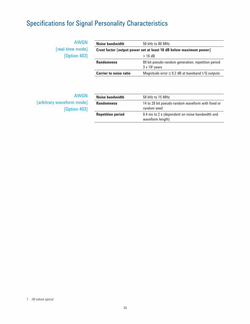
Specifications for Signal Personality Characteristics
AWGN[real-time mode]
[Option 403]
AWGN[arbitrary waveform mode]
[Option 403]
Noise bandwidth 50 kHz to 80 MHzCrest factor [output power set at least 16 dB below maximum power]
> 16 dBRandomness 89 bit pseudo-random generation, repetition period
3 x 10⁹ yearsCarrier to noise ratio Magnitude error ≤ 0.2 dB at baseband I/Q outputs
Noise bandwidth 50 kHz to 15 MHzRandomness 14 to 20 bit pseudo-random waveform with fixed or
random seedRepetition period 0.4 ms to 2 s (dependent on noise bandwidth and
waveform length)

24
Specifications for Signal Personality Characteristics
1. This level of performance can be attained using the external I/Q inputs, provided the quality of the baseband signal meets or exceeds that of the ESG baseband generator.
2. Parentheses denote typical performance.3. Specifications apply at power levels ≤ +4 dBm [≤ +5 dBm for Option 506, and ≤ +8 dBm for Option UNB] with
default scale factor of I/Q outputs.4. Valid after executing I/Q calibration and maintained within +/- 5 °C of the calibration temperature.5. ACP for TETRA is measured over a 25 kHz bandwidth, with an 18 kHz root raised cosine filter. Low ACP mode is
valid at power levels ≤ –1 dBm [≤ 1 dBm for Option 506 and ≤ +4 dBm for Option UNB].6. Specifications apply for the symbol rates, filter, filter factors [a or BbT] and default scaling factor specified for
each standard, and at power levels ≤ +7 dBm [≤ +10 dBm for Option UNB].7. The “channel spacing” determines the offset size of the adjacent and alternate channels: Adjacent channel
offset = 1 x channel spacing, 1st alternate channel = 2 x channel spacing, 2nd alternate channel = 3 x channel spacing, etc.
Custom modulation[real-time mode]
Custom digitally modulated signals [real-time mode] 1, 2
Internal modulation using real-time TDMA personalities [Option 402] 2
Modulation QPSK π/4DQPSK 16QAm 2FSK GMSKFilterFilter factor [α or BbT]
Root Nyquist Gaussian0.25 0.25 0.25 0.5 0.5
Modulation index N/A N/A N/A 0.5 N/ASymbol rate [Msym/s] 4 4 4 1 1
Error vector magnitude 3, 4
[% rms]Shift error 3, 4
[% rms]
Global phase error 3, 4
[degrees rms]fc = 1 GHzfc = 2 GHzfc = 3 GHzfc = 4 GHzfc = 5 GHzfc = 6 GHz
1.1 (0.7)1.2 (0.8)1.6 (1.0)2.5 (1.4)1.5 (1.0)1.8 (1.2)
1.1 (0.7)1.2 (0.8)1.6 (1.0)2.5 (1.3)1.5 (1.0)1.8 (1.2)
1.0 (0.6)1.0 (0.6)1.5 (0.9)3.3 (1.9)1.2 (0.8)2.0 (1.4)
1.3 (0.8)1.4 (0.9)1.8 (1.0)3.3 (2.0)1.8 (1.2)2.0 (1.4)
0.4 (0.2)0.5 (0.3)0.7 (0.4)1.0 (0.6)0.6 (0.3)0.8 (0.4)
NADC PDC PHS TETRA 4 DECT GSM DCS, PCS
EDGE
Error vector magnitude 6, 4 [% rms] Low EVM mode Low ACP mode
1.2 (0.7)(1.2)
1.2 (0.7)(0.9)
0.9 (0.5)(0.6)
0.8 (0.5)(1.0)
1.2 (0.6)
Global phase error 2 rms pk
N/A N/A N/A N/A N/A 0.6 (0.3)1.9 (1.0)
N/A
Deviation accuracy 2 [kHz, rms] N/A N/A N/A N/A 2.5 (1.1) N/A N/AChannel spacing [kHz] 30 25 300 25 1728 200 200Adjacent channel power 2 [ACP] (Low ACP mode, dBc) at adjacent channel 7
at 1st alternate channel 7
at 2nd alternate channel 7
at 3rd alternate channel 7
Cont. Burst Cont. Burst Cont. Burst Cont. Burst N/A Cont. Burst N/A
(–35)(–80)(–84)(–85)
(–34)(–79)(–83)(–84)
–(–74)
–(–82)
–(–74)
–(–82)
–(–81)(–82)
–
–(–76)(–79)
–
(–70)(–81)(–82)(–83)
(–63)(–80)(–82)(–83)
(–37)(–71)(–84)(–85)
(–37)(–70)(–81)(–81)
Support burst type Customup/down TCH
Customup/down TCH
up Vox
CustomTCH, sync
Customup control 1 & 2
up normal,down normal
Customdummy B 1 & 2
traffic B,low capacity
Custom, normal,
Fcorr, sync, dummy, access
Scramble burst type Yes Yes

25
Specifications for Signal Personality Characteristics
GSM/GPRS[real-time mode]
[Option 402]
Multiframe output data generation Coding scheme Full-rate speech [TCH/FS]
CS-1, CS-4 Data PN9 or PN15
The selected data sequence is coded continu-ously across the RLC data block as per ETSI TS 100 909, 3GPP TS 05.03, V8.9.0, 2000-11 [release 1999] An independent version of the selected data sequence is coded across the MAC header.
Frame structure 26-frame multi-frame structure as per ETSIGSM, 05.01 version 6.1.1 [1998-07].[Coding is done on frames 0-11, 13-24, of the multi-frame. Frame 25 is idle [RF blanked].]
Adjacent timeslots Data
Frame structure
PN9, PN15 coded as per ETSI TS 100 909, 3GPP TS 05.03, V8.9.0, 2000-11 [release 1999].
26-frame multi-frame structure as per ETSI GSM, 5.01 version 6.1.1 [1998-07].
Alternate time slot power level control[Valid for standard attenuator only. Not applicable to Option UNB or Option 506]Amplitude is settled within 0.5 dB in 20 µsecs, +4 to –136 dBm at 23 ±5 °C

26
Specifications for Signal Personality Characteristics
EDGE/EGPRS[real-time mode]
[Option 402]
Bit error rate [BER] analyzer[Option UN7]
Multiframe output data generation Coding scheme MCS-1: uplink and downlink, MCS-5: uplink and
downlink,MCS-9: uplink and downlink, E-TCH/F43.2
Data PN9 or PN15The selected data sequence is fully coded continuously across the RLC data blocks accord-ing to MCS-1, MCS-5, MCS-9 or E-TCH/F43.2. An independent version of the selected data sequence is coded across the unused RLC/MAC header fields [The CPS header field is as defined in GSM 04.60 V8.50].
Frame structure 52-frame multi-frame structure for EDGE/EGPRS channel as per ETSI TS 100 909, 3GPP TS 05.03, V8.9.0, 2000-11 [release 1999]. [Coding is done on frames 0-11, 13-24, 26-37, 39-50 on a 52 PDCH multi-frame. Frame 25 and 51 are idle [RF blanked].]
Adjacent timeslots Data
Frame structure
Coded MCS-1, MCS-5 or MCS-9 with continuous PN9 or PN15 sequence data payload.Uncoded PN9, PN15.Note: Maximum of 4 timeslots can be turned on with EDGE/EGPRS multi-frame coded data.
EDGE/EGPRS PDCH multi-frame.Repeating EDGE frame.
Clock rate 100 Hz to 60 MHzSupported data patterns PN9, 11, 15, 20, 23Resolution 10 DigitsBit sequence length 100 bits to 4,294 Gbits after synchronizationFeatures
Input clock phase adjustment and gate delayAdjustable input thresholdHi/lo threshold selectable from 0.7 V [TTL], 1.4 V [TTL] 1.65 V [CMOS 3.3], 2.5 V [CMOS 5.0]Direct measurement triggeringData and reference signal outputsReal-time displayBit countError-bit-count Bit error rate Pass/fail indication Valid data and clock detection Automatic re-synchronization Special pattern ignore
27
General Characteristics
Operating characteristics Power requirement 90 to 254 V; 50/60/400 Hz nominal; 200 W maximum
Operating temperature range 1
0 to 55 °C
Storage temperature range
–40 to 71 °C
Shock and vibration Meets MIL-STD-28800E Type III, Class 3Storage registers Memory is shared by instrument states, user
data files, non-volatile waveforms, sweep list files and waveform sequences. There is 14 MB of flash memory standard in the ESG. With Option 005, there is 6 GB of storage. Depending on available memory, a maximum of 1000 instru-ment states can be saved.
Weight < 16 kg [35 lb.] net, < 23 kg [50 lb.] shippingDimensions 133 mm H x 426 mm W x 432 mm D
[5.25 in H x 16.8 in W x 17 in D]Remote programming Interface
Control languages 2
Functions controlled
GPIB [IEEE-488.2-1987] with listen and talk, RS-232, LAN [10BaseT].
SCPI version 1996.0, also compatible with 8656B and 8657A/B/C/D/J1 mnemonics.
All front panel functions except power switch and knob.
ISO compliant The E4438C ESG is manufactured in an ISO-9001 registered facility in concurrence with Agilent Technologies commitment to quality.
Reverse power protection 3
SWR 4
Output impedance 50 Ω nominal
Options 501-504 Option 506250 kHz to 2 GHz> 2 to 4 GHz> 4 to 6 GHzMax DC voltage
47 dBm (50 W)44 dBm (25 W)
N/A50 V
30 dBm (1 W)30 dBm (1 W)30 dBm (1 W)
Options 501-504 Options 501-504with Option UNB
Option 506with Option UNB
250 kHz to 2.2 GHz> 2.2 GHz to 3 GHz> 3 GHz to 4 GHz> 4 GHz to 6 GHz
(< 1.5:1)(< 1.4:1)(< 1.5:1)
N/A
(< 1.5:1)(< 1.5:1)(< 1.7:1)
N/A
(< 1.6:1)(< 1.4:1)(< 1.7:1)(< 1.8:1)
1. Save and recall of user files and instrument states from non-volatile storage is guaranteed only over the range 0 to 40 °C.2. ESG series does not implement 8657A/B “Standby” or “On” [R0 or R1, respectively] mnemonics.3. Options 501-504 are protected to levels indicated, however, the reverse power protection circuit will trip at nominally 30 dBm (1 W).4. Parentheses denote typical performance.
28
General Characteristics
Accessories
Inputs and outputs
All front panel connectors can be moved to rear with Option 1EM.
Transits case Part number 9211-1296
10 MHz input Accepts a 1, 2, 5, or 10 MHz ±0.2 ppm [high-stability timebase] reference signal for operation with an external timebase. Nominal input level –3.5 to +20 dBm, impedance 50 Ω. [BNC, rear panel]
10 MHz output Outputs the 10 MHz reference signal. Level nominally +3.9 dBm ±2 dB. Nominal output impedance 50 Ω. [BNC, rear panel]
Alternate power input Accepts CMOS 1 signal for synchronization of external data and alternate power signal timing. The damage levels are –0.5 to +5.5 V. [Auxiliary I/O connector, rear panel]
Baseband generator reference input
Accepts 0 to +20 dBm sinewave, or TTL square-wave, to use as reference clock for the baseband generator. Phase locks the internal data genera-tor to the external reference; the RF frequency is still locked to the 10 MHz reference. Rate is 250 kHz to 100 MHz, 50 Ω nominal, AC coupled. [BNC, rear panel] [SMB with Option 1EM]
Burst gate input The burst gate in connector accepts a CMOS 1 signal for gating burst power in digital modula-tion applications. The burst gating is used when you are externally supplying data and clock infor-mation. The input signal must be synchronized with the external data input that will be output during the burst. The burst power envelope and modulated data are internally delayed and re-synchronized. The input signal must be CMOS high for normal burst RF power or CW RF output power and CMOS low for RF off. The damage levels are –0.5 to +5.5 V.
This female BNC connector is provided on signal generators with Option 601 or 602. On signal generators with Option 1EM, this input is relocated to a rear panel SMB connector. With Option 401, this connector is used for the even second synchronization input.
Coherent carrier output 2 Outputs RF modulated with FM or ΦM, but not IQ, pulse or AM. Nominal power –2 dBm ±5 dB. Nominal impedance 50 ohms. Frequency range from > 250 MHz to 4 GHz. For RF carriers below this range, output frequency = 1 GHz – frequency of RF output. Damage levels 20 VDC and 13 dBm reverse RF power. [SMA, rear panel]1. Rear panel inputs and outputs are 3.3 V
CMOS, unless indicated otherwise. CMOS inputs will accept 5 V CMOS, 3 V CMOS, or TTL voltage levels.
2. Coherent carrier is modulated by FM or FM when enabled.

29
General Characteristics
Data clock input The CMOS1 compatible data clock connector accepts an externally supplied data-clock input for digital modulation ap-plications. The expected input is a bit clock signal where the falling edge is used to clock the data and symbol sync signals.The maximum clock rate is 50 MHz. The damage levels are –0.5 to +5.5 V. This female BNC connector is provided on signal generators with Option 601 or 602. On signal generators with Option 1EM, this input is relocated to a rear panel SMB connector.
Data clock output Relays a CMOS1 bit clock signal for synchronizing serial data. [Auxiliary I/O connector, rear panel]
Data input The CMOS 1 compatible data connector accepts an externally supplied data input for digital modulation applications. CMOS high is equivalent to a data 1 and a CMOS low is equivalent to a data 0.The maximum data rate is 50 Mb/s. The data must be valid on the data clock falling edges [normal mode] or the symbol sync falling edges [symbol mode]. The damage levels are –0.5 to +5.5 V.This female BNC connector is provided on signal generators with Option 601 or 602. On signal generators with Option 1EM, this input is relocated to a rear panel SMB connector.
Data output Outputs serial data from the internal data generator or the externally supplied signal at the data input. CMOS 1 signal. [Auxiliary I/O connector, rear panel]
Event 1 output In real-time mode, outputs pattern or frame synchronization pulse for triggering or gating external equipment. May be set to start at the beginning of a pattern, frame, or timeslot and is adjustable to within ± one timeslot with one bit resolution. In arbitrary waveform mode, this connector outputs the timing signal generated by marker 1. [BNC, rear panel] [SMB with Option 1EM]
Event 2 output In real-time mode, outputs data enabled signal for gating external equipment. Applicable when external data is clocked into internally generated timeslots. Data is enabled when signal is low.In arbitrary waveform mode, this connector outputs the timing signal generated by marker 2. [BNC, rear panel] [SMB with Option 1EM]
Event 3 output In arbitrary waveform mode, this connector outputs the timing signal generated by marker 3. [Auxiliary I/O connector, rear panel]
Event 4 output In arbitrary waveform mode, this connector outputs the timing signal generated by marker 4. [Auxiliary I/O connector, rear panel]
1. Rear panel inputs and outputs are 3.3 V CMOS, unless indicated otherwise. CMOS inputs will accept 5 V CMOS, 3 V CMOS, or TTL voltage levels.
30
General Characteristics
External 1 input This BNC input connector accepts a ±1 Vpeak signal for AM, FM, pulse, burst, and phase modulation. For all these modula-tions, ±1 Vpeak produces the indicated deviation or depth. When ac-coupled inputs are selected for AM, FM, or phase modulation and the peak input voltage differs from 1 Vpeak by more than 3%, the hi/lo annunciator light on the display. The input impedance is 50 Ω and the damage levels are 5 Vrms and 10 Vpeak.If you configure your signal generator with Option 1EM, this input is relocated to a female SMB connector on the rear panel.
External 2 input This BNC input connector accepts a ±1 Vpeak signal for AM, FM, phase modulation, and pulse modulation. With AM, FM, or phase modulation, ±1 Vpeak produces the indicated deviation or depth. With pulse modulation, +1 V is on and 0 V is off. When ac-coupled inputs are selected for AM, FM, or phase modulation, and the peak voltage differs from 1 Vpeak by more than 3%, the hi/lo annunciator light on the display. The input impedance is 50 Ω and the damage levels are 5 Vrms and 10 Vpeak.If you configure your signal generator with Option 1EM, this input is relocated to a female SMB connector on the rear panel.
GPIB Allows communication with compatible devices. [rear panel]I input Accepts an I input either for I/Q modulation or for wideband
AM. Nominal input impedance 50 or 600 Ω. Damage levels are 1 Vrms and 10 Vpeak. [BNC, front panel] [SMB with Option 1EM]
I out and Q out 1 The I out and Q out connectors output the analog components of I/Q modulation from the internal baseband generator. The nominal output impedance of these connectors are 50 Ω, DC-coupled. The damage levels are > +3.5 V and < –3.5 V. The output signal levels into a 50 Ω load are as follows:
• (O.5 Vpeak,), corresponds to one unit length of the I/Q vector.
• (0.7 Vpeak ), for peaks for p/4 DQPSK.
• (1.6 Vp-p) maximum [Options 601, 602, 001, 002 only].
These female BNC connectors are provided on signal generators with Option 601 or 602. On signal generators with Option 1EM, these inputs are relocated to rear panel SMB connectors.
1. Parentheses denote typical performance.

31
General Characteristics
I and Q out I and Q are used in conjunction with I and Q to provide a bal-anced baseband stimulus. Balanced signals are signals pres-ent in two separate conductors that are symmetrical about the common mode offset, and are opposite in polarity [180 degrees out of phase].These female BNC connectors are provided only on signal generators with Option 601 or 602. If you configure your sig-nal generator with Option 1EM, these inputs are relocated to rear panel SMB connectors.
LF output Outputs the internally-generated LF source. Outputs 0 to 2.5 Vpeak into 50 Ω, or 0 to 5 Vpeak into high impedance. [BNC, front panel] [SMB with Option 1EM]
Pattern trigger input Accepts CMOS 1 signal to trigger internal pattern or frame generator to start single pattern output. Minimum pulse width 100 ns. The damage levels are –0.5 to +5.5 V. [BNC, rear panel] [SMB with Option 1EM]
Q input Accepts a Q input for I/Q modulation. Nominal input imped-ance 50 or 600 ohms, damage levels are 1 Vrms and 10 Vpeak. [BNC, front panel] [SMB with Option 1EM]
RF output Nominal output impedance 50 Ω. [type-N female, front panel]
Sweep output Generates output voltage, 0 to +10 V when signal genera-tor is sweeping. Output impedance < 1 Ω, can drive 2000 Ω. [BNC, rear panel] [SMB with Option 1EM]
Symbol sync input The CMOS 1 compatible symbol sync connector accepts an externally supplied symbol sync for digital modulation applica-tions. The expected input is a symbol clock signal. It may be used in two modes. When used as a symbol sync in conjunc-tion with a data clock, the signal must be high during the first data bit of the symbol. The signal must be valid during the falling edge of the data clock signal and may be a single pulse or continuous. When the symbol sync itself is used as the [symbol] clock, the falling edge is used to clock the data signal.The maximum clock rate is 50 MHz. The damage levels are –0.5 to +5.5 V. [BNC, front panel]This female BNC connector is provided on signal generators with Option 601 or 602. On signal generators with Option 1EM, this input is relocated to a rear panel SMB connector.
Symbol sync output Outputs CMOS 1 symbol clock for symbol synchronization, one data clock period wide. [Auxiliary I/O connector, rear panel]
Trigger input Accepts CMOS 1 signal for triggering point-to-point in manual sweep mode, or to trigger start of LF sweep. the damage lev-els are –0.5 to +5.5 V. [BNC, rear panel]
Trigger output Outputs a TTL signal: high at start of dwell, or when waiting for point trigger in manual sweep mode; low when dwell is over or point trigger is received, high or low 2 µs pulse at start of LF sweep. [BNC, rear panel]
1. Rear panel inputs and outputs are 3.3 V CMOS, unless indicated otherwise. CMOS inputs will accept 5 V CMOS, 3 V CMOS, or TTL voltage levels.

32
General Characteristics
With Option UN7 BER data, BER clock BER gate
BER sync loss output
BER no data output
BER error-bit-output
BER test result output
BER measure end output
BER measure trigger
Accepts CMOS 1 or 75 Ω input. Polarity is selected. Clock duty and inputs cycle is 30% to 70%. [SMB, rear panel]
Outputs a CMOS 1 signal that is low when sync is lost. Valid only when measure end signal is high. [Auxiliary I/O connector, rear panel]
Outputs a CMOS 1 signal that is low when no data is detect-ed. Valid only when measure end is high. [Auxiliary I/O connector, rear panel]
Outputs CMOS 1 signal when error bit is detected. Pulse width matches the input clock. [Auxiliary I/O connector, rear panel]
Outputs a CMOS 1 signal that is high for fail and low for pass. Valid only on measure end signal falling edge. [Auxiliary I/O connector, rear panel]
Outputs a CMOS 1 signal that is high during measurement. Trigger events are ignored while high.[Auxiliary I/O connector, rear panel]
Accepts CMOS 1 signal to initiate BER measurement. Polarity is selectable; available when trigger source is selected as “AUX I/O”. Damage levels are The damage levels are –0.5 to +5.5 V. [Auxiliary I/O connector, rear panel]
With Option 300 321.4 MHz input Accepts a 321.4 MHz IF signal for GSM/EDGE/loopback test-
ing. Input amplitude range -7 dBm to -22 dBm. Nominal input impedance 50 Ω. [SMB, rear panel]
LAN connector
LAN communication is supported by the signal generator via the LAN connector. It is functionally equivalent to the GPIB connector. The LAN connector enables the signal generator to be remotely programmed by a LAN-connected computer. The distance between a computer and the signal generator is limited to 100 meters [10BaseT]. For more information about the LAN, refer to the Getting Started chapter in the Programming Guide. Data transfer speeds 2
LAN [FTP] file transfer to volatile memory (700 KB/sec)to hard drive (500 KB/sec)
LAN [SCPI] command transfer to volatile memory (146 KB/sec)to hard drive (128 KB/sec)
Internal file transfer from hard drive to volatile memory (1280 KB/sec)Agilent’s IO Libraries Suite ships with the E4438C to help you quickly establish an error-free con-nection between your PC and instruments – regardless of the vendor. It provides robust instru-ment control and works with the software development environment you choose.
1. Rear panel inputs and outputs are 3.3 V CMOS, unless indicated otherwise. CMOS inputs will accept 5 V CMOS, 3 V CMOS, or TTL voltage levels.
2. Parentheses denote typical performance.

33
RS-232 connector
This male DB-9 connector is an RS-232 serial port that can be used for controlling the signal generator remotely. It is functionally equivalent to the GPIB connector. The following table shows the description of the pinouts. The pin configuration is shown below. Pin number Signal description Signal name 1 No connection 2 Receive data RECV 3 Transmit data XMIT 4 +5 V 5 Ground, 0 V 6 No connection 7 Request to send RTS 8 Clear to send CTS 9 No connection
View looking into rear panel connectorAuxiliary I/O connector
This male DB-9 connector is an RS-232 serial port that can be used for controlling the signal generator remotely. It is functionally equivalent to the GPIB connector. The following table shows the description of the pinouts. The pin configuration is shown below.
View looking into rear panel connectorMating connector 37 pin male D-subminiature, available from AMP, 3M, others.
General Characteristics
5 4 3 2 1
9 8 7 6
Event 3
Event 4
Patt trig in 2
Alt pwr in
Parallel data 1*
GND
GND
GND
GND
GND
Parallel data 8*
Parallel data clk*
Data out
Data clk out
Sym sync out
BER sync loss
GND (BER)
GND (BER)
BER meas end
GND
GND
GND
GND
Parallel data 2*
Parallel data 3*
Parallel data 4*
Parallel data 5*
Parallel data 6*
Parallel data 7*
GND
GND
GND
GND
GND
BER meas trig/BER no data
BER err out
BER test out
3719
201
*Future capability
34
Ordering Information 1
Performance enhancement options
System accessories
Embedded signal creation software 3, 4
PC-based signal creation software 3, 4
Baseband products 5
• 501 1 GHz frequency range• 502 2 GHz frequency range• 503 3 GHz frequency range• 504 4 GHz frequency range• 506 6 GHz frequency range [requires option UNJ, includes mechanical attenuator]• UNB High output power with mechanical attenuator [optional with 501, 502, 503, 504]
[included with 506]• UNJ Enhanced phase noise performance [includes 1E5]• 1E5 High-stability time base• 1EM Moves all front panel connectors to rear• 003 2 Enables ESG digital outputs with N5102A• 004 2 Enables ESG digital inputs with N5102A• 601 Internal baseband generator with 8 MSa and digital bus capability [40 MB] of memory• 602 Internal baseband generator with 64 MSa and digital bus capability [320 MB] of memory• 005 3 6 GB internal hard drive• UN7 Internal bit-error-rate analyzer• 1CP Rack mount kit with handles• 1CN Front handle kit• E4438C-400 3GPP W-CDMA with HSDPA • E4438C-401 cdma2000 and IS-95A • E4438C-402 TDMA (GSM, GPRS, EDGE, EGPRS, DADC, PCD, PHS, TETRA, DECT) • E4438C-403 calibrated noise • E4438C-409 GPS• E4438C-422 scenario generator for GPS• E4438C-221 to 229 waveform license 5-packs• E4438C-250 to 259 waveform license 50-packs• E4438C-407 Signal Studio for S-DMB • E4438C-419 Signal Studio for 3GPP W-CDMA HSPA • E4438C-SP1 Signal Studio for Jitter Injection • N7600B Signal Studio for 3GPP W-CDMA FDD• N7601B Signal Studio for 3GPP2 CDMA• N7602B Signal Studio for GSM/EDGE• N7606B Signal Studio for Bluetooth ™• N7611B Signal Studio for Broadcast Radio• N7612B Signal Studio for TD-SCDMA• N7613A Signal Studio for 802.16-2004 (WiMAX ™ )• N7615B Signal Studio for 802.16 WiMAX• N7616B Signal Studio for T-DMB• N7617B Signal Studio for 802.11 WLAN• N7620A Signal Studio for Pulse Building• N7621B Signal Studio for Multitone Distortion• N7622A Signal Studio Toolkit• N7623B Signal Studio for Digital Video• N7624B Signal Studio for 3GPP LTE• N7625B Signal Studio for 3GPP LTE TDD• N5102A digital signal interface module• N5106A PXB baseband generator and channel emulator
1. All options should be ordered using E4438C-xxx, where the xxx represents the option number. For more information, please refer to the configuration guide publication number 5988-4085EN.
2. Requires either Option 601 or 602 (baseband generator) to function.3. Requires Option 001, 002, 601, or 602.4. For the latest information visit www.agilent.com/find/signalstudio.5. For details visit www.agilent.com/find/basebandstudio and www.agilent.com/find/PXB.
35
Related Literature
Application literature
Product literature
• 3GPP Long Term Evolution: System Overview, Product Development and Test Challenges, literature number 5989-8139EN, May 2008.
• BER and Subjective Evaluation for DVB-T/H Receiver Test, literature number 5989-8446EN, May 2008.
• Typical GPS Receiver Verification Tests Using a GPS Signal Simulator, literature number 5989-8572EN, May 2008.
• Designing and Testing 3GPP W-CDMA Base Transceiver Stations, Application Note 1355, literature number 5980-1239E, March 2006.
• MIMO Channel Modeling and Emulation Test Challenges, literature number 5989-8973EN, October 2008.
• RF Source Basics, a self-paced tutorial (CD-ROM), literature number 5980-2060E, October 2000.
• Digital Modulation in Communications Systems—An Introduction, Application Note 1298, literature number 5965-7160E, October 2000.
• Using Vector Modulation Analysis in the Integration, Troubleshooting and Design of Digital Communications Systems, Product Note, literature number 5091-8687E, March 2001.
• Testing CDMA Base Station Amplifiers, Application Note 1307, literature number 5967-5486E May 2000.
• Understanding GSM/EDGE Transmitter and Receiver Measurements for Base Transceiver Stations and Their Components, Application Note 1312, literature number 5968-2320E August 2002.
• Understanding CDMA Measurements for Base Stations and their Components, Application Note 1311, literature number 5968-0953E, June 2000.
• Testing and Troubleshooting Digital RF Communications Receiver Designs, Application Note 1314, literature number 5968-3579E, March 2002.
Additional application literature may be found by going to www.agilent.com/find/signalstudio and selecting the "Library" tab.
• E4438C ESG Vector Signal Generator, Brochure, literature number 5988-3935EN.
• E4438C ESG Vector Signal Generator, Configuration Guide, literature number 5988-4085EN.
• Agilent MXG Signal Generator, Brochure, literature number 5989-5074EN.
• Agilent MXG Signal Generator, Configuration Guide, literature number 5989-5485EN.
• Agilent N5182A MXG Vector Signal Generator, Data Sheet, literature number 5989-5261EN.
• Agilent N5106A PXB MIMO Receiver Tester, Data Sheet, literature number 5989-8971EN.
• Agilent N5106A PXB MIMO Receiver Tester, Configuration Guide, literature number 5989-8972EN.

cdma2000 is a registered certification mark of the Telecommunications Industry Association. Used under license.
Bluetooth and the Bluetooth logos are trademarks owned by Bluetooth SIG, Inc., U.S.A. and licensed to Agilent Technologies, Inc.
WiMAX, Mobile WiMAX, and WiMAX Forum are trademarks of the WiMAX Forum.
www.agilent.com/find/emailupdatesGet the latest information on the products and applications you select.
www.lxistandard.orgLAN eXtensions for Instruments puts the power of Ethernet and the Web inside your test systems. Agilent is a founding member of the LXI consortium.
Agilent Channel Partnerswww.agilent.com/find/channelpartnersGet the best of both worlds: Agilent’s measurement expertise and product breadth, combined with channel partner convenience.
www.agilent.comwww.agilent.com/find/esg
Agilent Advantage Services is committed to your success throughout your equip-ment’s lifetime. To keep you competitive, we continually invest in tools and processes that speed up calibration and repair and reduce your cost of ownership. You can also use Infoline Web Services to manage equipment and services more effectively. By sharing our measurement and service expertise, we help you create the products that change our world.
www.agilent.com/quality
www.agilent.com/find/advantageservices
For more information on Agilent Technologies’ products, applications or services, please contact your local Agilent office. The complete list is available at:www.agilent.com/find/contactus
AmericasCanada (877) 894 4414 Brazil (11) 4197 3600Mexico 01800 5064 800 United States (800) 829 4444
Asia PacificAustralia 1 800 629 485China 800 810 0189Hong Kong 800 938 693India 1 800 112 929Japan 0120 (421) 345Korea 080 769 0800Malaysia 1 800 888 848Singapore 1 800 375 8100Taiwan 0800 047 866Other AP Countries (65) 375 8100
Europe & Middle EastBelgium 32 (0) 2 404 93 40 Denmark 45 45 80 12 15Finland 358 (0) 10 855 2100France 0825 010 700* *0.125 €/minuteGermany 49 (0) 7031 464 6333 Ireland 1890 924 204Israel 972-3-9288-504/544Italy 39 02 92 60 8484Netherlands 31 (0) 20 547 2111Spain 34 (91) 631 3300Sweden 0200-88 22 55United Kingdom 44 (0) 118 927 6201For other unlisted countries: www.agilent.com/find/contactusRevised: January 6, 2012
Product specifications and descriptions in this document subject to change without notice.
© Agilent Technologies, Inc. 2012Published in USA, May 21, 20125988-4039EN