advance controlling and monitoring system
TRANSCRIPT
Project report
on
Advance Controlling And Monitoring SystemSubmitted in the partial fulfillment for award of degree of
Bachelor of Technology
in
ELECTRONICS AND COMMUNICATION branch of
MAHARISHI DAYANAND UNIVERSITY, ROHTAK
Submitted by:-
Anil Kumar 7EC-133L
Manjari Sharma 7EC-138L
Yatin Kumar 7EC-145L
Anuj Tyagi 7EC-147
Department of Electronics and Communication Engineering
Lingaya’s Institute of Management And Technology
Nachauli, Old Faridabad-Jasana Road, Faridabad – 121002, India
May 2011
LINGAYA'S INSTITUTE OF MANAGEMENT AND TECHNOLOGY
CERTIFICATE OF AUTHENTICATION
This is to certify that project Associates Anil Kumar(7EC-133L), Manjari Sharma(7EC-138L), Yatin Kumar (7EC-145L), Anuj Tyagi(7EC-147) of Bachelor of technology 8th Sem. ELECTRONICS & COMMUNICATION branch have successfully completed the Project-“ADVANCE CONTROLLING AND MONITORING SYSTEM” which is the authentic record of their own work under the supervision of Mr. Monimoy Dutta in the partial fulfillment for the award of Bachelor of Technology from MAHRSHI DAYANAND UNIVERSITY, ROHTAK during the academic year 2007-2011. The matter presented in this report has not been submitted by them in any other university/institute for the award of B.Tech Degree. We wish them a prosperous happy & bright future with all the great silvery success in their career.
(HOD, Elec. & Comm). (Project Guide) (Project CO-ORDINATOR) (Mr. K.S. Mathur) (Mr. Monimoy Dutta) (Mr. M.K. Jain )

ACKNOWLEDGEMENT
“To the accomplishment of any feat is required a medium of hard work. An optima of motivation and an extreme of guidance the ocean, has to take up the right course least it ends up in enduary.”
Behind the successful completion of our project there are number of people whom we would like to thank. We would like to express our gratitude & sincere thanks providing us the necessary infrastructure.
We, ANIL KUMAR (7EC 133-L), MANJARI SHARMA (7EC 138-L), YATIN KUMAR (7EC 145-L) and ANUJ TYAGI (7EC 147) are thankful to Mr. S.V.A.V. Prasad Dean of academic affair, LIMAT and Mr. K.S. Mathur, Head of deppt. ECE, LIMAT for the kind support that they extended to us for making this project.
We owe a sincere thank to our project guide Mr. Monimoy Dutta and our Project Co-ordinator Mr. M.K. Jain. We are also thankful to Mr. Ramnarayan and Mr. Prajapati for their co-operation, kindness and general help extended to us during the completion of this work.
SUBMITTED BY:-
Anil Kumar (7EC-133L)
Manjari Sharma (7EC-138L)
Yatin Kumar (7EC-145L)
Anuj Tyagi (7EC-147)
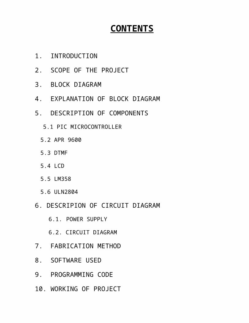
CONTENTS
1. INTRODUCTION
2. SCOPE OF THE PROJECT
3. BLOCK DIAGRAM
4. EXPLANATION OF BLOCK DIAGRAM
5. DESCRIPTION OF COMPONENTS
5.1 PIC MICROCONTROLLER
5.2 APR 9600
5.3 DTMF
5.4 LCD
5.5 LM358
5.6 ULN2804
6. DESCRIPION OF CIRCUIT DIAGRAM
6.1. POWER SUPPLY
6.2. CIRCUIT DIAGRAM
7. FABRICATION METHOD
8. SOFTWARE USED
9. PROGRAMMING CODE
10. WORKING OF PROJECT
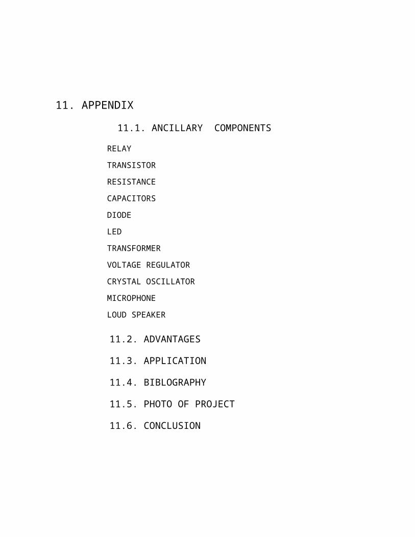
11. APPENDIX
11.1. ANCILLARY COMPONENTS
RELAY
TRANSISTOR
RESISTANCE
CAPACITORS
DIODE
LED
TRANSFORMER
VOLTAGE REGULATOR
CRYSTAL OSCILLATOR
MICROPHONE
LOUD SPEAKER
11.2. ADVANTAGES
11.3. APPLICATION
11.4. BIBLOGRAPHY
11.5. PHOTO OF PROJECT
11.6. CONCLUSION
INTRODUCTION
Turning a mobile phone into a multifunctional remote control centre. Imagine turning on your air conditioner at home before entering the house; our programming your VCR from mall orca, using your phone. Not any more! Up to now, these “teleaction” systems have been very expensive and limited to business application, such as factory security and machine control. But we are now time to offer telematic system for mass market as well. Even the installation is simple; this device connects the home telemetry equipment to the public telephone network.
Control modules from variety of manufacture have been on the market for same time, although, until now, they have required special transmitter for activation. The residential gateway now enables any type of house hold equipment, from entrance telephone, to be easily control from a remote location (either inside the house or st the distance) using the telephone keypad. You can even determine the equipments status (on or off) from any location.
“The residential gateway is a prime example of how information technology and communication are merging”. The interface enables a virtually unlimited number of application to be activated or accessed from a remote location, which means that the target group for these products is “enormous”. More and more people want greater convenience or are frequently away from house or business or personal reason, for want to protect valuable possessions such as vacation home or sailboat by remote control. And the trend is rising rapidly for personal mobility is increasing just as fast, if not faster, in society.
Here is a micro controller based, versatile circuit through which we control the home appliances in our absence. In this project two section are presents one is the transmitter and the second is the receiver section. When the signal sends from the transmitter then the receiver send the status in the form of sound signal related to that appliance This project is made due to the fact kipping in mind to solve the upcoming problem in the field of controlling equipments from the certain distance or any part of the world.
By implementing this technique we can control machinery through our phone, the status of particular of our particular equipment on/off. The project is advantages is giving us many benefits like saving time, money, and electricity and avoid accidents.
This system detects the ringing signal from your exchange with the help of ring detector and automatically switches ON. This device saves your money. This circuit switches off after a time of 60 second (you can change this switch ON time which is discussed in detail in coming section).
Before changing the state of device we can confirm the present status of the device. This circuit gives an acknowledgment tone after switching On the device to confirm the status of the device.
SCOP OF THE PROJECT
“Advance Controlling and Monitoring System” can be modified by connecting it
with a personal computer. This will help the user to get the whole data stored in
computer’s memory and the user will be able to check the whole record anytime.
For doing this, we have to make the database in our computer to store all the data
in the which will be done using Visual Basics. The whole data such as when the
particular appliance switched on and when it is switched off will get stored in
computer.
The database in the computer will let us know about the switching record of
appliance with date, time and duration for which they are being operated and with
the help of speech software we can also give acknowledgement to user about the
status of appliance or device.
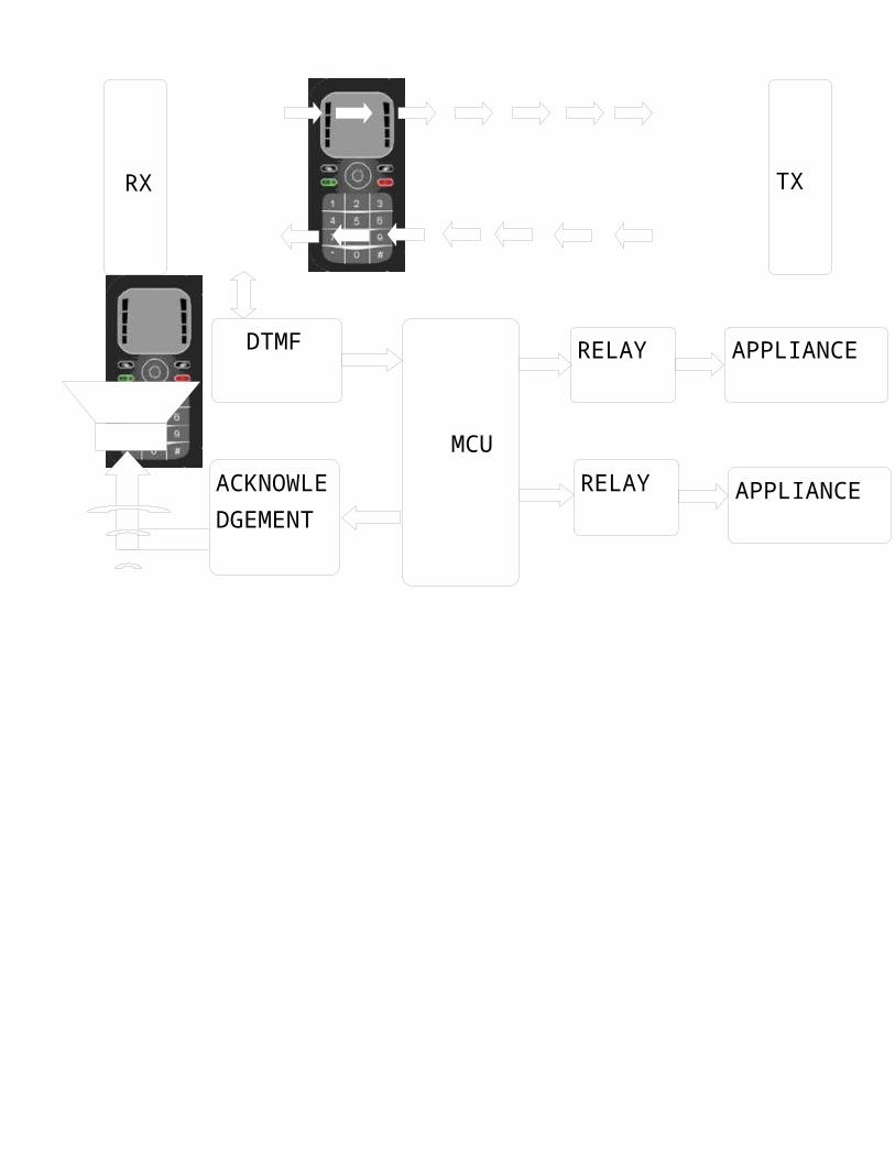
BLOCK DIAGRAM
ACKNOWLEDGEMENT
DTMF
RELAY APPLIANCE
APPLIANCERELAY
MCU
TX RX
EXPANATION OF BLOCK DIAGRAM
This project will overcome the disadvantages of the radio frequency system which have short distance communication and the short frequency. Here is a micro controller based, versatile circuit through which we control the home appliances in our absence. In this project two section are presents one is the transmitter and the second is the receiver section. When the signal sends from the transmitter then the receiver send the status in the form of sound signal related to that appliance. After getting the status we can ON or OFF that appliance.
In the block diagram of advance controlling and monitoring system there are two mobile phone in which one act as transmitter and other act as the receiver. When the call is made by the mobile at the transmitter then the call is automatically received at the receiver as it is in the auto-answering mode.
After the call is received at the receiver then a key is pressed on the keypad of the mobile that will generate a DTMF tone which is the summation of two frequencies (upper and lower frequency). This tone is known as Dual Tone Multiple Frequency. This DTMF tone is first given to the LM358 which is used to amplify the signal at the receiver mobile.
Then this DTMF tone is given to the DTMF decoder (MT8870) at the two inputs of the decoder IC in corresponding to that four binary output at the pin 11, 12, 13, 14 and the 15 pin is for the indication of the signal is received by the IC or not.
After we get output from the decoder IC is then provided to the microcontroller PIC16F877A which is the 40 pin flash microcontroller.
The microcontroller act as the brain of the circuit through by doing appropriate programming we can control the respective appliances.

Here we use the combination of the mobile keys. For ex.-- * with n for status check, 0 with n for ON the appliance and # with n for OFF the appliances. One most important feature of our project is that we can get the acknowledgement at the transmitter mobile phone in the form of sound with the help of APR9600 which is the recording and playback IC.
We can record eight message and according to the microcontroller programming we can get the sound acknowledgement. With the help of coding in microcontroller we can know either our appliance is ON or OFF and according to which we can switch appliances ON or OFF from the distance place.
LM-358
LM358 is a Low Power Dual Operational Amplifier. Internally frequency compensated operational amplifiers which were designed specifically to operate from a single power supply over a wide range of voltages. The purpose of using this I.C is to amplify the input signal coming from mobile phone which is attached to the circuit.
MT 8870
We are using MT8870 as a DTMF decoder IC which is used to decode the analog signal into the binary outputs. The DTMF stands for Dual Tone Multiple frequency.
The M-8870 is a full DTMF Receiver that integrates both bandsplit filter and decoder functions into a single 18-pin DIP or SOIC package. Manufactured using CMOS process technology, the M-8870 offers low power consumption (35 mW max) and precise data handling. Its decoder uses digital counting techniques to detect and decode all 16 DTMF tone pairs into a 4-bit code.
PIC 16F877A
The microcontroller which is used in our project is PIC16F877A which is a 40-Pin Enhanced FLASH Microcontroller.PIC stands for PERIPHERAL INTERFACE CONTROLLER. This is an 8 bit microcontroller which has almost all the features to meet user’s requirement and is used in wide range of applications
The main function of this microcontroller is to control the peripherals attached to it according to the user’s requirement. In our project when DTMF signal is provided to microcontroller then according to the programming part corresponding action is taken. Suppose if we press 1 then the binary output of DTMF goes to controller and according to our programming the pin which is attached to relay 1 is switched on.
APR-9600
The APR9600 device offers true single-chip voice recording, non-volatile storage, and playback capability for 40 to 60 seconds. The function of this I.C is to play the recorded message which is already stored in it. According to the signal fixed in programming of controller will play the message like if we press 7 then the message recorded on APR’s 1st or 2nd pin is played and let us know about the status of appliance.
ULN-2804
ULN2804 is a HIGH-VOLTAGE, HIGH-CURRENT DARLINGTON ARRAYS. All devices are pinned with outputs opposite inputs to facilitate ease of circuit board layout. In our circuit we are using it to drive relays. The output of this I.C is parallel to input which provide ease to us to operate many relays corresponding to
the signal’s output from microcontroller.
DESCRIPTION
OF
COMPONENTS
Microcontroller PIC16F877A :-
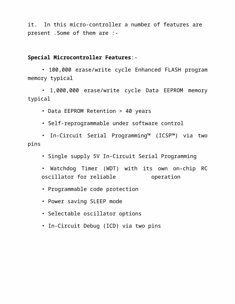
In this project we have use the pic micro-controller PIC16F877A . PIC (PERIPHERAL INTERFACE CONTROLLER) 8 bit MCU series is one of the most effective and demanded MCU’s unit as they are being used in wide range of applications these days and have almost all other features for which make user stick to it. In this micro-controller a number of features are present .Some of them are :-
Special Microcontroller Features:-
• 100,000 erase/write cycle Enhanced FLASH program memory typical
• 1,000,000 erase/write cycle Data EEPROM memory typical
• Data EEPROM Retention > 40 years
• Self-reprogrammable under software control
• In-Circuit Serial Programming™ (ICSP™) via two pins
• Single supply 5V In-Circuit Serial Programming
• Watchdog Timer (WDT) with its own on-chip RC oscillator for reliable operation
• Programmable code protection
• Power saving SLEEP mode
• Selectable oscillator options
• In-Circuit Debug (ICD) via two pins
Peripheral Features:-
• Timer0: 8-bit timer/counter with 8-bit pre scaler
• Timer1: 16-bit timer/counter with prescalar , can be incremented during SLEEP via external crystal/clock
• Timer2: 8-bit timer/counter with 8-bit period register, prescaler and postscaler
• Two Capture, Compare, PWM modules
- Capture is 16-bit, max. Resolution is 12.5 ns
- Compare is 16-bit, max. Resolution is 200 ns
- PWM max. resolution is 10-bit
• Synchronous Serial Port (SSP) with SPI™ (Master mode) and2C™(Master/Slave)
• Universal Synchronous Asynchronous Receiver Transmitter (USART/SCI) with 9-bit address detection
• Parallel Slave Port (PSP) 8-bits wide, with external RD, WR and CS controls (40/44-pin only)
• Brown-out detection circuitry for Brown-out Reset (BOR) Device Program Memory Data
Analog Features:-
• 10-bit, up to 8 channel Analog-to-Digital Converter (A/D)
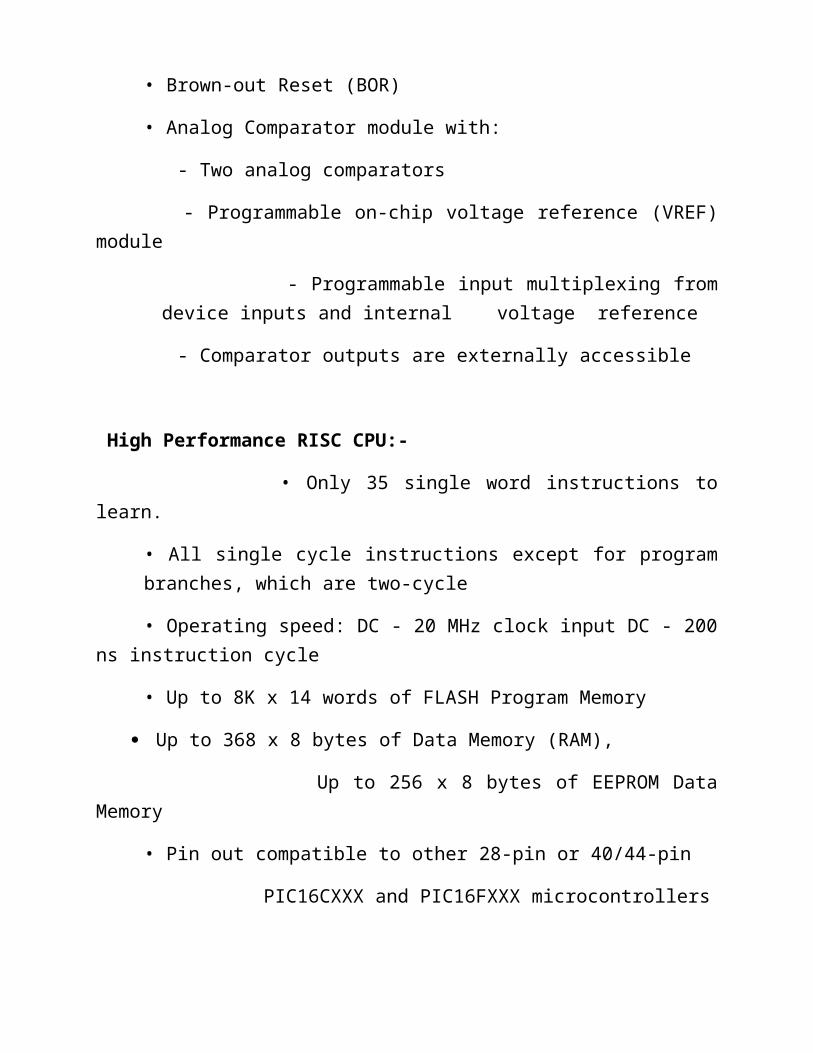
• Brown-out Reset (BOR)
• Analog Comparator module with:
- Two analog comparators
- Programmable on-chip voltage reference (VREF) module
- Programmable input multiplexing from device inputs and internal voltage reference
- Comparator outputs are externally accessible
High Performance RISC CPU:-
• Only 35 single word instructions to learn.
• All single cycle instructions except for program branches, which are two-cycle
• Operating speed: DC - 20 MHz clock input DC - 200 ns instruction cycle
• Up to 8K x 14 words of FLASH Program Memory
Up to 368 x 8 bytes of Data Memory (RAM),
Up to 256 x 8 bytes of EEPROM Data Memory
• Pin out compatible to other 28-pin or 40/44-pin
PIC16CXXX and PIC16FXXX microcontrollers
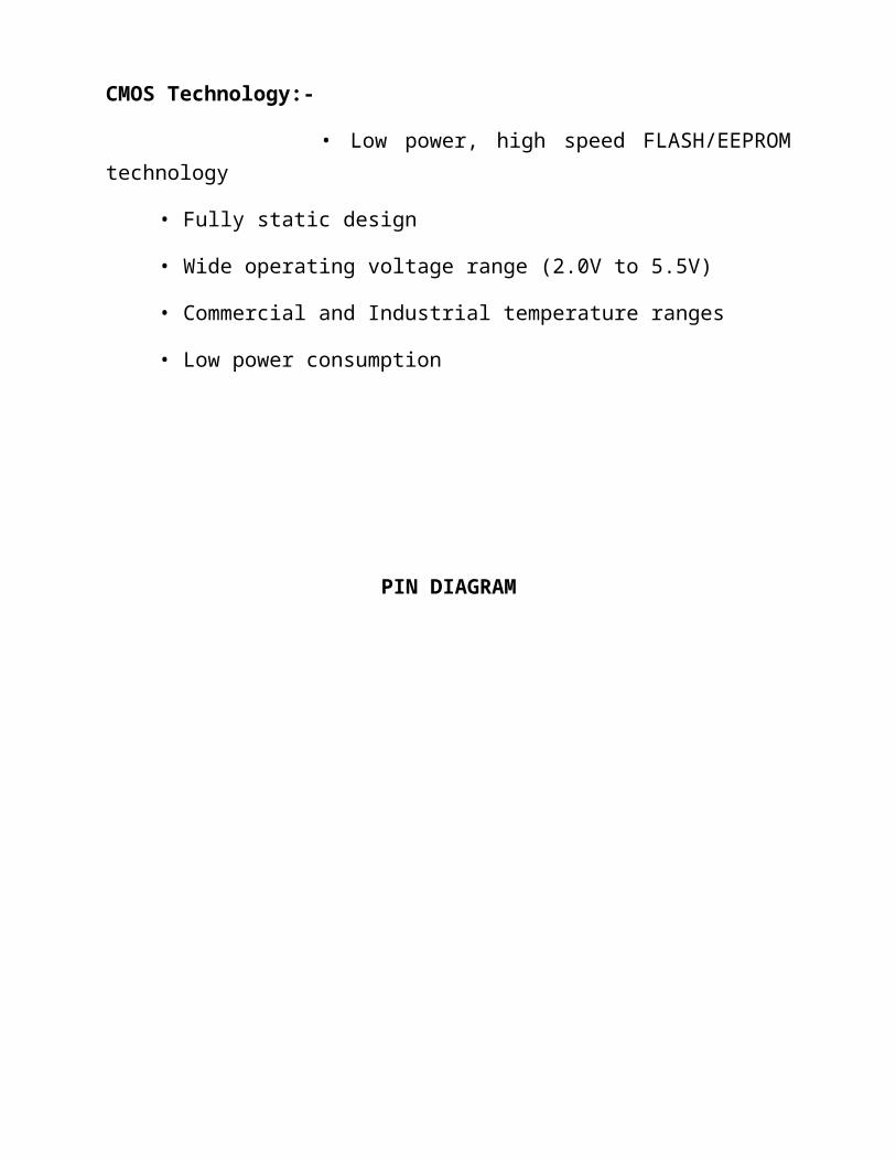
CMOS Technology:-
• Low power, high speed FLASH/EEPROM technology
• Fully static design
• Wide operating voltage range (2.0V to 5.5V)
• Commercial and Industrial temperature ranges
• Low power consumption
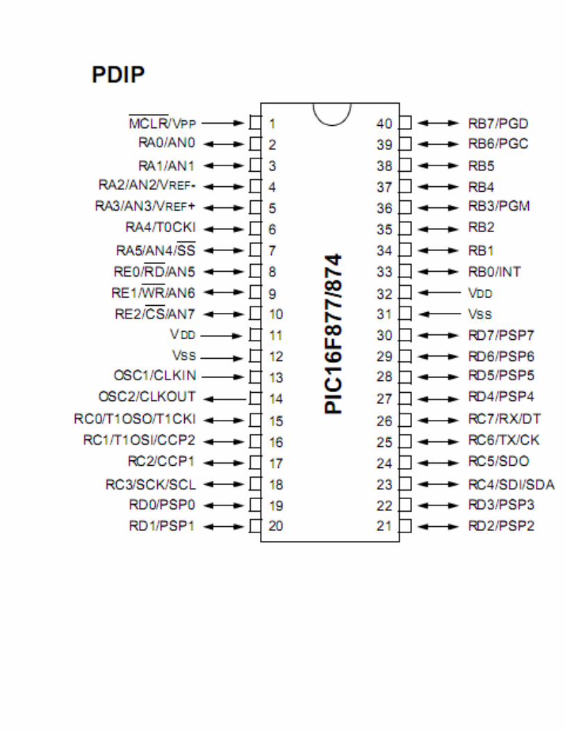
PIN DIAGRAM
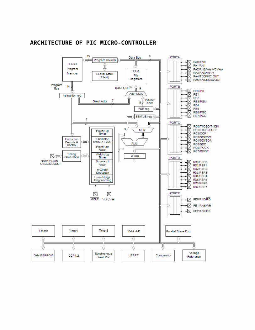
ARCHITECTURE OF PIC MICRO-CONTROLLER
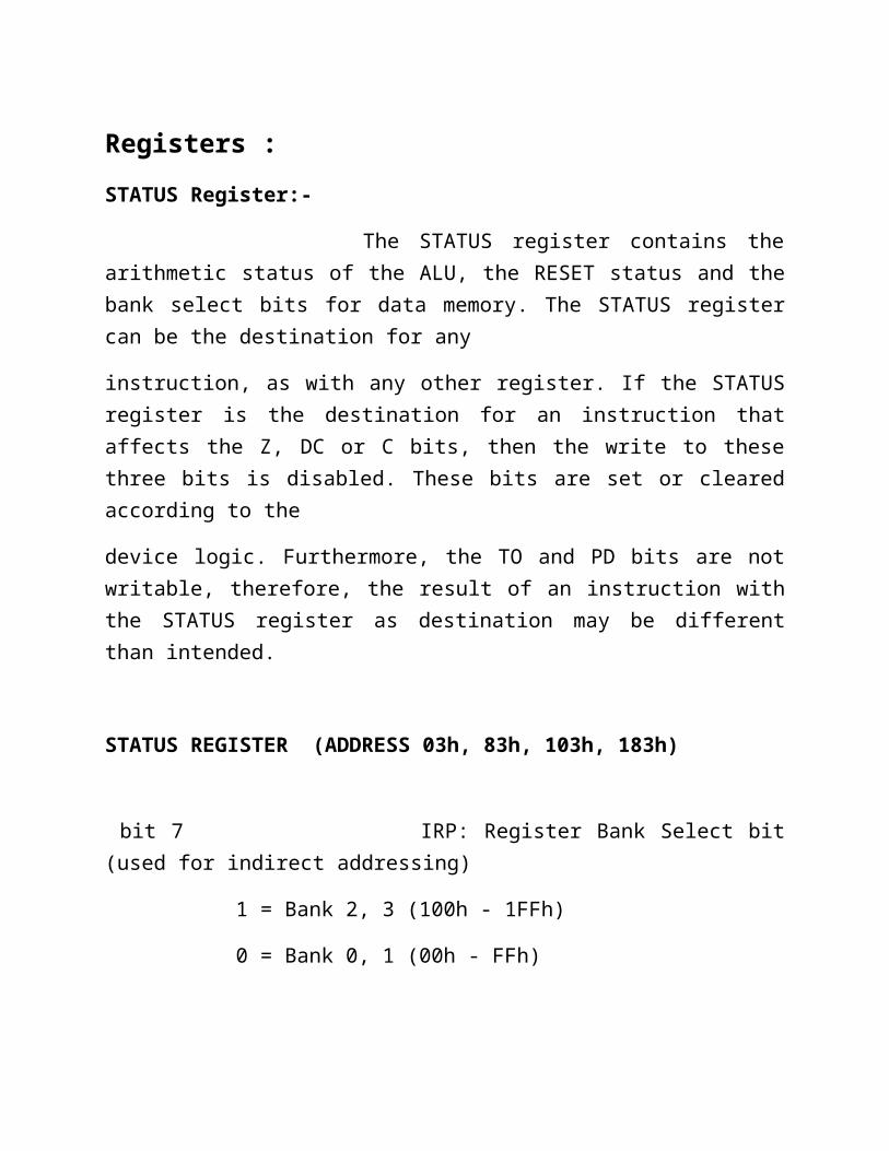
Registers :
STATUS Register:-
The STATUS register contains the arithmetic status of the ALU, the RESET status and the bank select bits for data memory. The STATUS register can be the destination for any
instruction, as with any other register. If the STATUS register is the destination for an instruction that affects the Z, DC or C bits, then the write to these three bits is disabled. These bits are set or cleared according to the
device logic. Furthermore, the TO and PD bits are not writable, therefore, the result of an instruction with the STATUS register as destination may be different than intended.
STATUS REGISTER (ADDRESS 03h, 83h, 103h, 183h)
bit 7 IRP: Register Bank Select bit (used for indirect addressing)
1 = Bank 2, 3 (100h - 1FFh)
0 = Bank 0, 1 (00h - FFh)
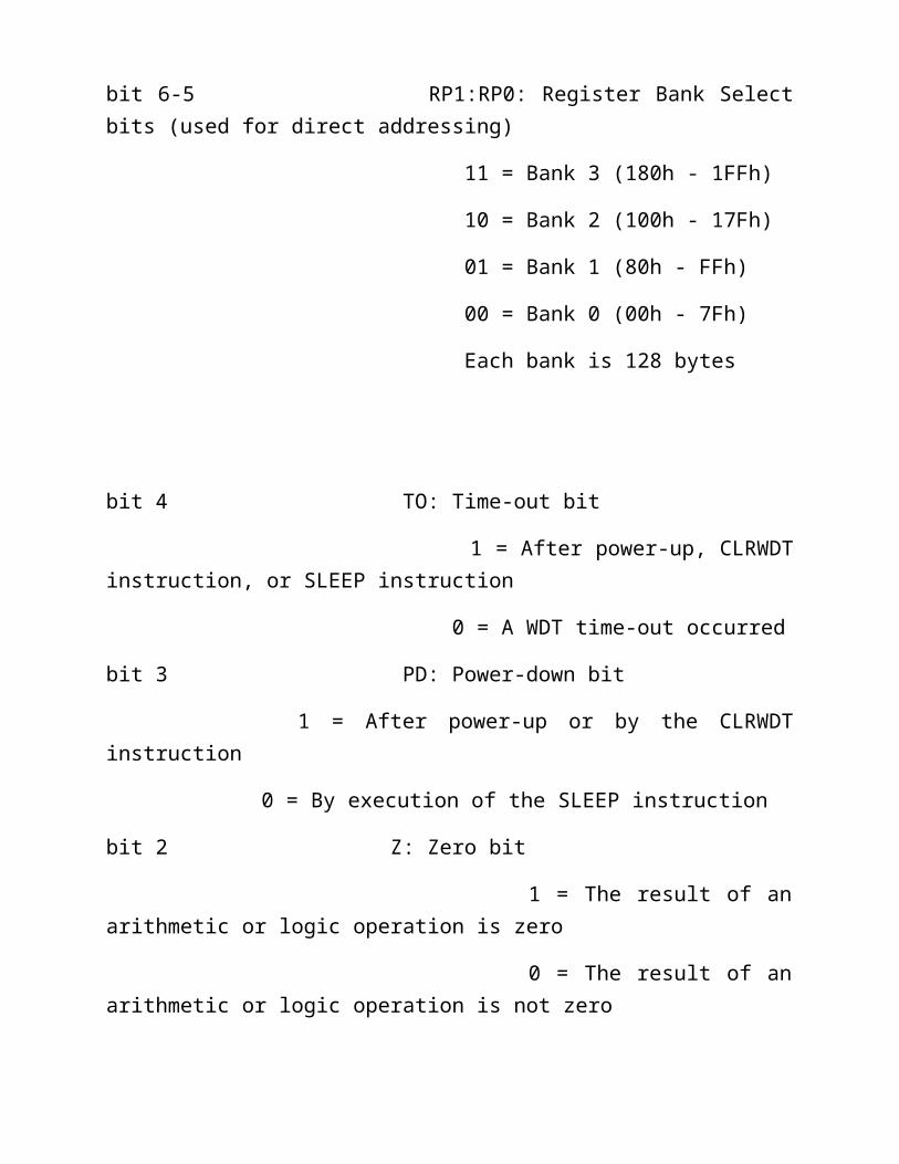
bit 6-5 RP1:RP0: Register Bank Select bits (used for direct addressing)
11 = Bank 3 (180h - 1FFh)
10 = Bank 2 (100h - 17Fh)
01 = Bank 1 (80h - FFh)
00 = Bank 0 (00h - 7Fh)
Each bank is 128 bytes

bit 4 TO: Time-out bit
1 = After power-up, CLRWDT instruction, or SLEEP instruction
0 = A WDT time-out occurred
bit 3 PD: Power-down bit
1 = After power-up or by the CLRWDT instruction
0 = By execution of the SLEEP instruction
bit 2 Z: Zero bit
1 = The result of an arithmetic or logic operation is zero
0 = The result of an arithmetic or logic operation is not zero
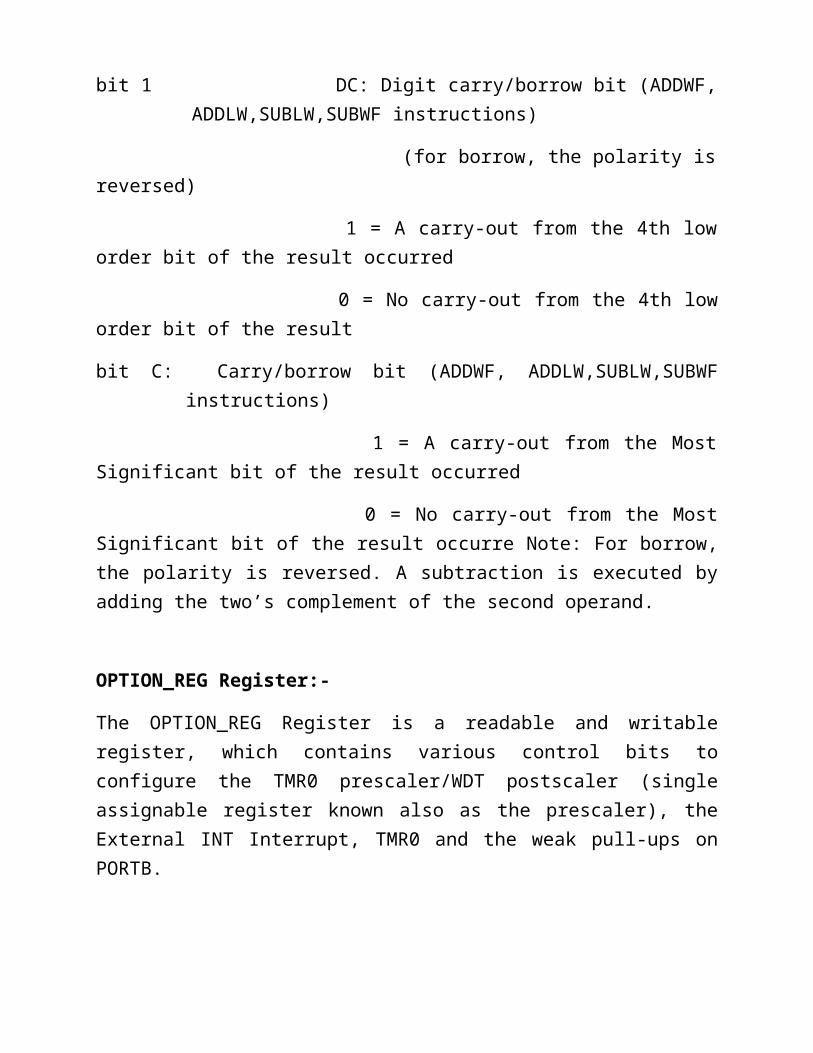
bit 1 DC: Digit carry/borrow bit (ADDWF, ADDLW,SUBLW,SUBWF instructions)
(for borrow, the polarity is reversed)
1 = A carry-out from the 4th low order bit of the result occurred
0 = No carry-out from the 4th low order bit of the result
bit C: Carry/borrow bit (ADDWF, ADDLW,SUBLW,SUBWF instructions)
1 = A carry-out from the Most Significant bit of the result occurred
0 = No carry-out from the Most Significant bit of the result occurre Note: For borrow, the polarity is reversed. A subtraction is executed by adding the two’s complement of the second operand.
OPTION_REG Register:-
The OPTION_REG Register is a readable and writable register, which contains various control bits to configure the TMR0 prescaler/WDT postscaler (single
assignable register known also as the prescaler), the External INT Interrupt, TMR0 and the weak pull-ups on PORTB.
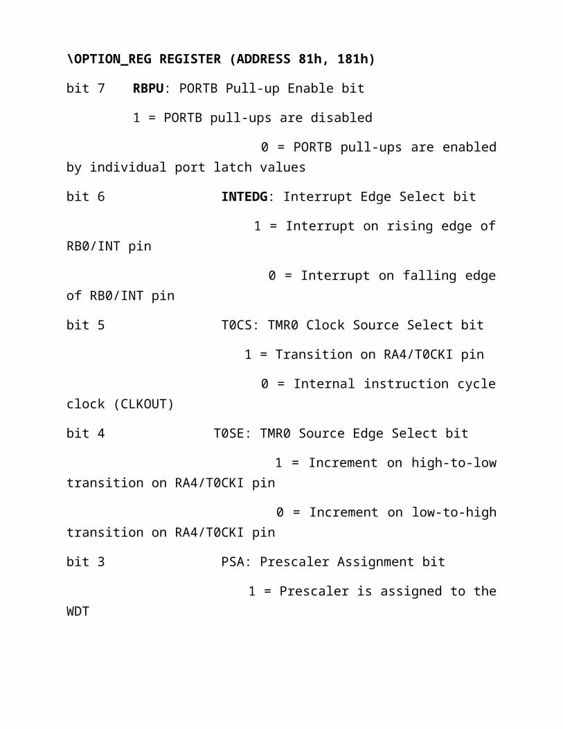
\OPTION_REG REGISTER (ADDRESS 81h, 181h)
bit 7 RBPU: PORTB Pull-up Enable bit
1 = PORTB pull-ups are disabled
0 = PORTB pull-ups are enabled by individual port latch values
bit 6 INTEDG: Interrupt Edge Select bit
1 = Interrupt on rising edge of RB0/INT pin
0 = Interrupt on falling edge of RB0/INT pin
bit 5 T0CS: TMR0 Clock Source Select bit
1 = Transition on RA4/T0CKI pin
0 = Internal instruction cycle clock (CLKOUT)
bit 4 T0SE: TMR0 Source Edge Select bit
1 = Increment on high-to-low transition on RA4/T0CKI pin
0 = Increment on low-to-high transition on RA4/T0CKI pin
bit 3 PSA: Prescaler Assignment bit
1 = Prescaler is assigned to the WDT
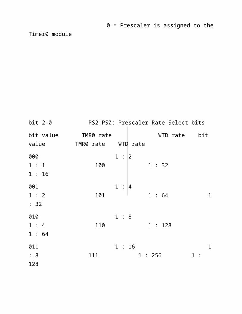
0 = Prescaler is assigned to the Timer0 module
bit 2-0 PS2:PS0: Prescaler Rate Select bits
bit value TMR0 rate WTD rate bit value TMR0 rate WTD rate
000 1 : 2 1 : 1 100 1 : 32 1 : 16
001 1 : 4 1 : 2 101 1 : 64 1 : 32
010 1 : 8 1 : 4 110 1 : 128 1 : 64
011 1 : 16 1 : 8 111 1 : 256 1 : 128
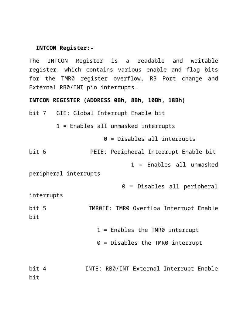
INTCON Register:-
The INTCON Register is a readable and writable register, which contains various enable and flag bits for the TMR0 register overflow, RB Port change and External RB0/INT pin interrupts.
INTCON REGISTER (ADDRESS 0Bh, 8Bh, 10Bh, 18Bh)
bit 7 GIE: Global Interrupt Enable bit
1 = Enables all unmasked interrupts
0 = Disables all interrupts
bit 6 PEIE: Peripheral Interrupt Enable bit
1 = Enables all unmasked peripheral interrupts
0 = Disables all peripheral interrupts
bit 5 TMR0IE: TMR0 Overflow Interrupt Enable bit
1 = Enables the TMR0 interrupt
0 = Disables the TMR0 interrupt
bit 4 INTE: RB0/INT External Interrupt Enable bit
1 = Enables the RB0/INT external interrupt
0 = Disables the RB0/INT external interrupt
bit 3 RBIE: RB Port Change Interrupt Enable bit
1 = Enables the RB port change interrupt
0 = Disables the RB port change interrupt
bit 2 TMR0IF: TMR0 Overflow Interrupt Flag bit
1 = TMR0 register has overflowed (must be cleared in software)
0 = TMR0 register did not overflow
bit 1 INTF: RB0/INT External Interrupt Flag bit
1 = The RB0/INT external interrupt occurred (must be cleared in software)
0 = The RB0/INT external interrupt did not occur
bit 0 RBIF: RB Port Change Interrupt Flag bit
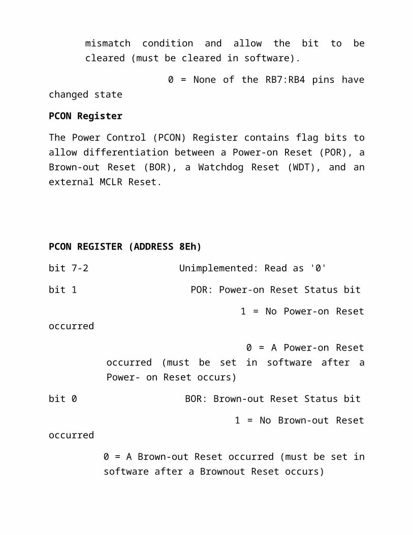
1 = At least one of the RB7:RB4 pins changed state; a mismatch condition will continue to set the bit. Reading PORTB will end the mismatch condition and allow the bit to be cleared (must be cleared in software).
0 = None of the RB7:RB4 pins have changed state
PCON Register
The Power Control (PCON) Register contains flag bits to allow differentiation between a Power-on Reset (POR), a Brown-out Reset (BOR), a Watchdog Reset (WDT), and an external MCLR Reset.
PCON REGISTER (ADDRESS 8Eh)
bit 7-2 Unimplemented: Read as '0'
bit 1 POR: Power-on Reset Status bit
1 = No Power-on Reset occurred
0 = A Power-on Reset occurred (must be set in software after a Power- on Reset occurs)
bit 0 BOR: Brown-out Reset Status bit
1 = No Brown-out Reset occurred
0 = A Brown-out Reset occurred (must be set in software after a Brownout Reset occurs)
PCL and PCLATH :-
The program counter (PC) is 13 bits wide. The low bytecomes from the PCL register, which is a readable andwritable register. The upper bits (PC<12:8>) are not readable, but are indirectly writable through thePCLATH register. On any RESET, the upper bits of the PC will be cleared.
STACK :-
The PIC16F87XA family has an 8-level deep x 13-bit wide hardware stack. The stack space is not part of either program or data space and the stack pointer is not readable or writable. The PC is PUSHed onto the stack when a CALL instruction is executed, or an interrupt causes a branch. The stack is POPed in the event of a RETURN, RETLW or a RETFIE instruction execution. PCLATH is not affected by a PUSH or POP operation. The stack operates as a circular buffer. This means that after the stack has been PUSHed eight times, the ninth push overwrites the value that was stored from the first push. The tenth push overwrites the second push (and so on).
DATA EEPROM AND FLASH PROGRAM MEMORY :-
The Data EEPROM and FLASH Program memory is readable and writable during normal operation (over the full VDD range). This memory is not directly mapped in the register file space. Instead, it is indirectly addressed through the Special Function Registers.
There are six SFRs used to read and write this memory:
•EECON1
•EECON2
•EEDATA
•EEDATH
•EEADR
•EEADRH
When interfacing to the data memory block, EEDATA holds the 8-bit data for read/write, and EEADR holds the address of the EEPROM location being accessed. These devices have 128 or 256 bytes of data EEPROM (depending on the device), with an address range from 00h to FFh. On devices with 128 bytes, addresses from 80h to FFh are unimplemented and will wrap around to the beginning of data EEPROM memory. When writing to unimplemented locations, the on-chip charge pump will be turned off.
When interfacing the program memory block, the EEDATA and EEDATH registers form a two-byte word that holds the 14-bit data for read/write, and the EEADR and EEADRH registers form a two-byte word that holds the 13-bit address of the program memory location being accessed. These devices have 4 or 8K words of program FLASH with an address range from 0000h to 0FFFh for the PIC16F873A/874A, and 0000h to 1FFFh for the PIC16F876A/877A. Addresses above the range of the respective device will wrap around to the beginning of program memory. The EEPROM data memory allows single byte read and write. The FLASH program memory allows single word reads and four-word block writes. Program memory write operations automatically perform an erase before-write on blocks of four words. A byte write in data EEPROM memory automatically erases the location and writes the new data (erase before write). The write time is controlled by an on-chip timer. The write/erase voltages are generated
by an on chip charge pump, rated to operate over the voltage range of the device for byte or word operations.When the device is code protected, the CPU may continue to read and write the data EEPROM memory. Depending on the settings of the write protect bits, the device may or may not be able to write certain blocks of the program memory; however, reads of the program memory are allowed. When code protected, the device programmer can no longer access data or program memory; this does NOT inhibit internal reads or writes.
Reading Data EEPROM Memory:-
To read a data memory location, the user must write the address to the EEADR register, clear the EEPGD control bit (EECON1<7>), and then set control bit RD(EECON1<0>). The data is available in the very next cycle, in the EEDATA register; therefore, it can be read in the next instruction (see Example3-1). EEDATA will hold this value until another read, or until it is written to by the user (during a write operation).
The steps to reading the EEPROM data memory are:
1. Write the address to EEADR. Make sure that theaddress is not larger than the memory size of the device.
2. Clear the EEPGD bit to point to EEPROM data memory.
3. Set the RD bit to start the read operation.
4. Read the data from the EEDATA register.
Writing to Data EEPROM Memory:-
To write an EEPROM data location, the user must first write the address to the EEADR register and the data to the EEDATA register. Then the user must follow a specific write sequence to initiate the write for each byte.
The write will not initiate if the write sequence is not exactly followed (write 55h to EECON2, write AAh to EECON2, then set WR bit) for each byte. We strongly recommend that interrupts be disabled during this code segment.
Additionally, the WREN bit in EECON1 must be set to enable write. This mechanism prevents accidental writes to data EEPROM due to errant (unexpected) code execution (i.e., lost programs). The user should keep the WREN bit clear at
all times, except when updating EEPROM. The WREN bit is not cleared by hardware
After a write sequence has been initiated, clearing the WREN bit will not affect this write cycle. The WR bit will be inhibited from being set unless the WREN bit is set. At the completion of the write cycle, the WR bit is cleared in hardware and the EE Write Complete Interrupt Flag bit (EEIF) is set. The user can either enable this interrupt or poll this bit. EEIF must be cleared by software.
The steps to write to EEPROM data memory are:
1. If step 10 is not implemented, check the WR bit to see if a write is in progress.
2. Write the address to EEADR. Make sure that the address is not larger than the memory size of the device.
3. Write the 8-bit data value to be programmed in the EEDATA register.4. Clear the EEPGD bit to point to EEPROM data memory.
5. Set the WREN bit to enable program operations.
6. Disable interrupts (if enabled).
7. Execute the special five instruction sequence:
• Write 55h to EECON2 in two steps (first to W, then to EECON2)
• Write AAh to EECON2 in two steps (first to W, then to EECON2)
• Set the WR bit
8. Enable interrupts (if using interrupts).
9. Clear the WREN bit to disable program operations.
10. At the completion of the write cycle, the WR bit is cleared and the EEIF interrupt flag bit is set.
(EEIF must be cleared by firmware.) If step 1 is not implemented, then firmware should check for EEIF to be set, or WR to clear, to indicate the end of the program cycle.
Reading FLASH Program Memory To read a program memory location, the user must write two bytes of the address to the EEADR and EEADRH registers, set the EEPGD control bit (EECON1<7>), and then set control bit RD (EECON1<0>). Once the read control bit is set, the program memory FLASH controller will use the next two instruction cycles to read the data. This causes these two instructions immediately following the “BSF EECON1,RD” instruction to be ignored. The data is available in the very next cycle, in the EEDATA and EEDATH registers; therefore, it can be read as two bytes in the following instructions. EEDATA and EEDATH registers will hold this value until another read or until it is written to by the user (during a write operation).
Writing to FLASH Program Memory
FLASH program memory may only be written to if the destination address is in a segment of memory that is not write protected, as defined in bits WRT1:WRT0 of the device configuration word (Register14-1). FLASH program memory must be written in four-word blocks.
A block consists of four words with sequential addresses, with a lower boundary defined by an address, where EEADR<1:0> = ‘00’. At the same time, all block writes to program memory are done as erase and write operations. The write operation is edge aligned, and cannot occur across boundaries.
To write program data, it must first be loaded into the buffer registers (see Figure3-1). This is accomplished by first writing the destination address to EEADR and EEADRH, and then writing the data to EEDATA and EEDATH. After the address and data have been set up, then the following sequence of events must be executed:
1. Set the EEPGD control bit (EECON1<7>)
2. Write 55h, then AAh, to EECON2 (FLASH programming sequence)
3. Set the WR control bit (EECON1<1>)
All four buffer register locations MUST be written to with correct data. If only one, two, or three words are being written to in the block of four words, then a read from the program memory location(s) not being written to must be performed. This takes the data from the program location(s) not being written and loads it into the
EEDATA and EEDATH registers. Then the sequence of events to transfer data to the buffer registers must be executed.
To transfer data from the buffer registers to the program memory, the EEADR and EEADRH must point to the last location in the four-word block (EEADR<1:0> =‘11’). Then the following sequence of events must be executed:
1. Set the EEPGD control bit (EECON1<7>)
2. Write 55h, then AAh, to EECON2 (FLASH programming sequence)
3. Set control bit WR (EECON1<1>) to begin the write operation
The user must follow the same specific sequence to initiate the write for each word in the program block, writing each program word in sequence (00,01,10,11).
When the write is performed on the last word (EEADR<1:0> = ‘11’), the block of four words are automatically erased, and the contents of the buffer registers are written into the program memory.
After the “BSF EECON1, WR” instruction, the processor requires two cycles to set up the erase/write operation.
The user must place two NOP instructions after the WR bit is set. Since data is being written to buffer registers, the writing of the first three words of the block appears to occur immediately. The processor will halt internal operations for the typical 4ms, only during the cycle in which the erase takes place (i.e., the last word of the four-word block). This is not SLEEP mode, as the clocks and peripherals will continue to run. After the write cycle, the processor will resume operation with the third instruction after the EECON1 write instruction. If the sequence is performed to any other location, the action is ignored.4.0I/O PORTS
Some pins for these I/O ports are multiplexed with an alternate function for the peripheral features on the device. In general, when a peripheral is enabled, that pin may not be used as a general purpose I/O pin. Additional information on I/O ports may be found in the PICmicro™ Mid-Range Reference Manual (DS33023).
APR9600
General Description:-
The APR9600 device offers true single chip voice recording, non-volatile storage, and playback capability for 40 to 60 seconds. The device supports both random and sequential access of multiple messages. Sample rates are user-select-able, allowing designers to customize their design for unique quality and storage time needs. Integrated output amplifier, microphone amplifier, and AGC circuits greatly simplify system design. The device is ideal for use in portable voice recorders, toys, and many other consumer and industrial applications.
Features:-
1. Single-chip, high-quality voice recording & playback solution
(i) No external ICs required
(ii) Minimum external components
2. Non-volatile Flash memory technology
(i) No battery backup required
3. User-Selectable messaging options
(i) Random access of multiple fixed-duration messages
(ii) Sequential access of multiple variable-duration messages
4. User-friendly, easy-to-use operation
(i)Programming & development systems not required
(ii) Level-activated recording & edge-activated play back switches

5. Low power consumption
(i) Operating current: 25 mA typical
(ii) Standby current: 1 uA typical
(iii) Automatic power-down
6. Chip Enable pin for simple message expansion
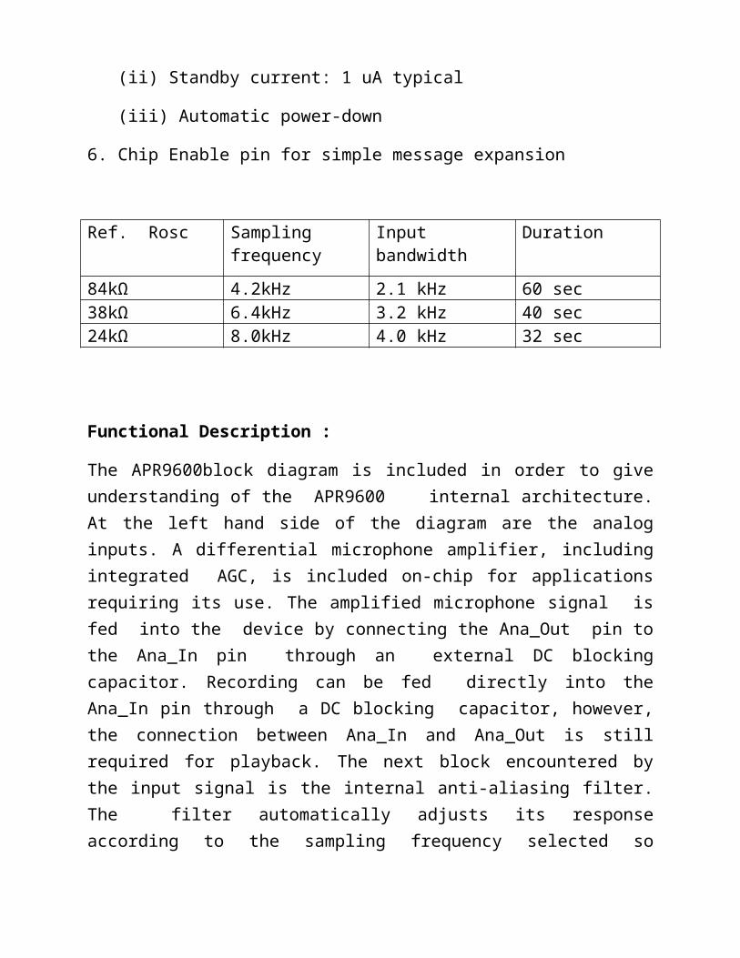
Ref. Rosc Sampling frequency
Input bandwidth Duration
84kΩ 4.2kHz 2.1 kHz 60 sec38kΩ 6.4kHz 3.2 kHz 40 sec24kΩ 8.0kHz 4.0 kHz 32 sec
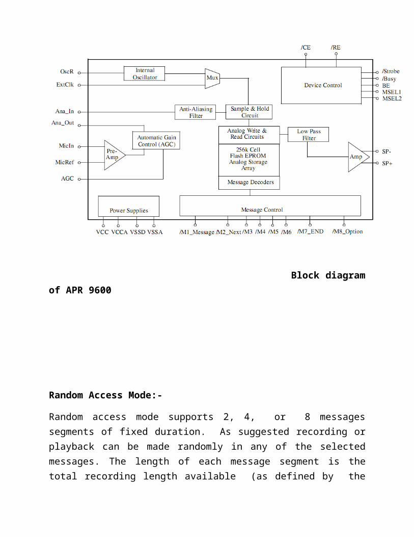
Functional Description :
The APR9600block diagram is included in order to give understanding of the APR9600 internal architecture. At the left hand side of the diagram are the analog inputs. A differential microphone amplifier, including integrated AGC, is included on-chip for applications requiring its use. The amplified microphone signal is fed into the device by connecting the Ana_Out pin to the Ana_In pin through an external DC blocking capacitor. Recording can be fed directly into the Ana_In pin through a DC blocking capacitor, however, the connection between Ana_In and Ana_Out is still required for playback. The next block encountered by the input signal is the internal anti-aliasing filter. The filter automatically adjusts its response according to the sampling frequency selected so Shannon’s Sampling Theorem is satisfied. After anti-aliasing filtering is accomplished the signal is ready to be clocked into the memory array. This storage is accomplished through a combination of the Sample and Hold circuit and the Analog Write/Read circuit. These circuits are clocked by either the Internal Oscillator or an external clock source. When playback is desired the previously stored recording is retrieved from memory, low pass filtered, and amplified as shown on the right hand side of the diagram. The signal can be heard by connecting a speaker to the SP+ and SP-
pins. Chip-wide management is accomplished through the device control block shown in the upper right hand corner.
Message management is controlled through the message control block represented in the lower center of the block diagram. More detailon actual device application can be found in the Sample Applications section. More detail on sampling control can be found in the Sample Rate and Voice Quality section. More detail on message management and device control can befound in the Message Management section.
Block diagram of APR 9600
Random Access Mode:-
Random access mode supports 2, 4, or 8 messages segments of fixed duration. As suggested recording or playback can be made randomly in any of the selected messages. The length of each message segment is the total recording length available (as defined by the selected sampling rate) divided by the total number of segments enabled. Random access mode provides easy indexing to message segments.
Functional Description of Recording in Random Access Mode
On power up, the device is ready to record or play back, in any of the enabled message segments. To record, /CE must be set low to enable the device and /RE must be set low to enable recording. You initiate recording by applying a low level on the message trigger pin that represents the message segment you intend to use. The message trigger pins are labeled /M1_Message - /M8_Option on pins 1-9 (excluding pin 7) for message segments 1-8 respectively. Note: Message trigger pins /M1_Message, /M2_Next, /M7_END, and /M8_Option, have expanded names to represent the different functionality that these pins assume in the other modes. In random access mode these pins should be considered purely message trigger pins with the same functionality as /M3, /M4, /M5, and /M6. For a more thorough explanation of the functionality of device pins in different modes please refer to the pin description table that appears later in this document.
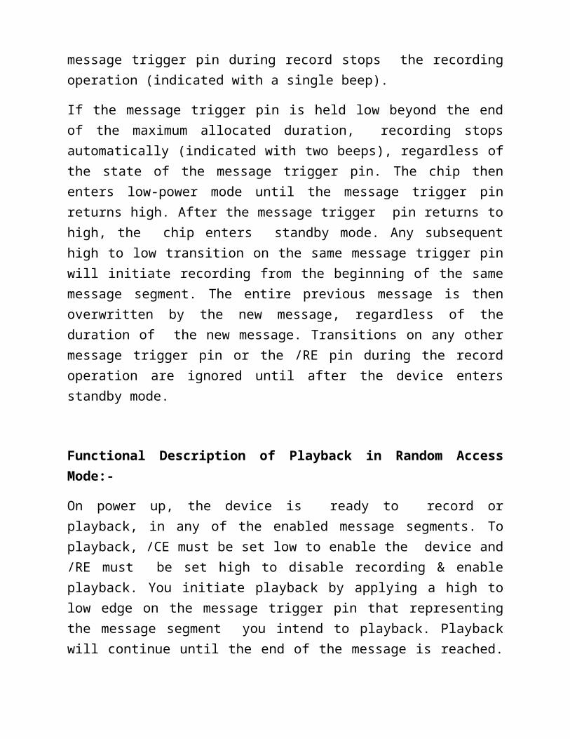
When actual recording begins the device responds with a single beep (if the BE pin is high to enable the beep tone) at the speaker outputs to indicate that it has started recording. Recording continues as long as the message pin stays low. The rising edge of the same message trigger pin during record stops the recording operation (indicated with a single beep).
If the message trigger pin is held low beyond the end of the maximum allocated duration, recording stops automatically (indicated with two beeps), regardless of the state of the message trigger pin. The chip then enters low-power mode until the message trigger pin returns high. After the message trigger pin returns to high, the chip enters standby mode. Any subsequent high to low transition on the same message trigger pin will initiate recording from the beginning of the same message segment. The entire previous message is then overwritten by the new message, regardless of the duration of the new message. Transitions on any other message
trigger pin or the /RE pin during the record operation are ignored until after the device enters standby mode.
Functional Description of Playback in Random Access Mode:-
On power up, the device is ready to record or playback, in any of the enabled message segments. To playback, /CE must be set low to enable the device and /RE must be set high to disable recording & enable playback. You initiate playback by applying a high to low edge on the message trigger pin that representing the message segment you intend to playback. Playback will continue until the end of the message is reached. If a high to low edge occurs on the same message trigger pin during playback, playback of the current message stops immediately.
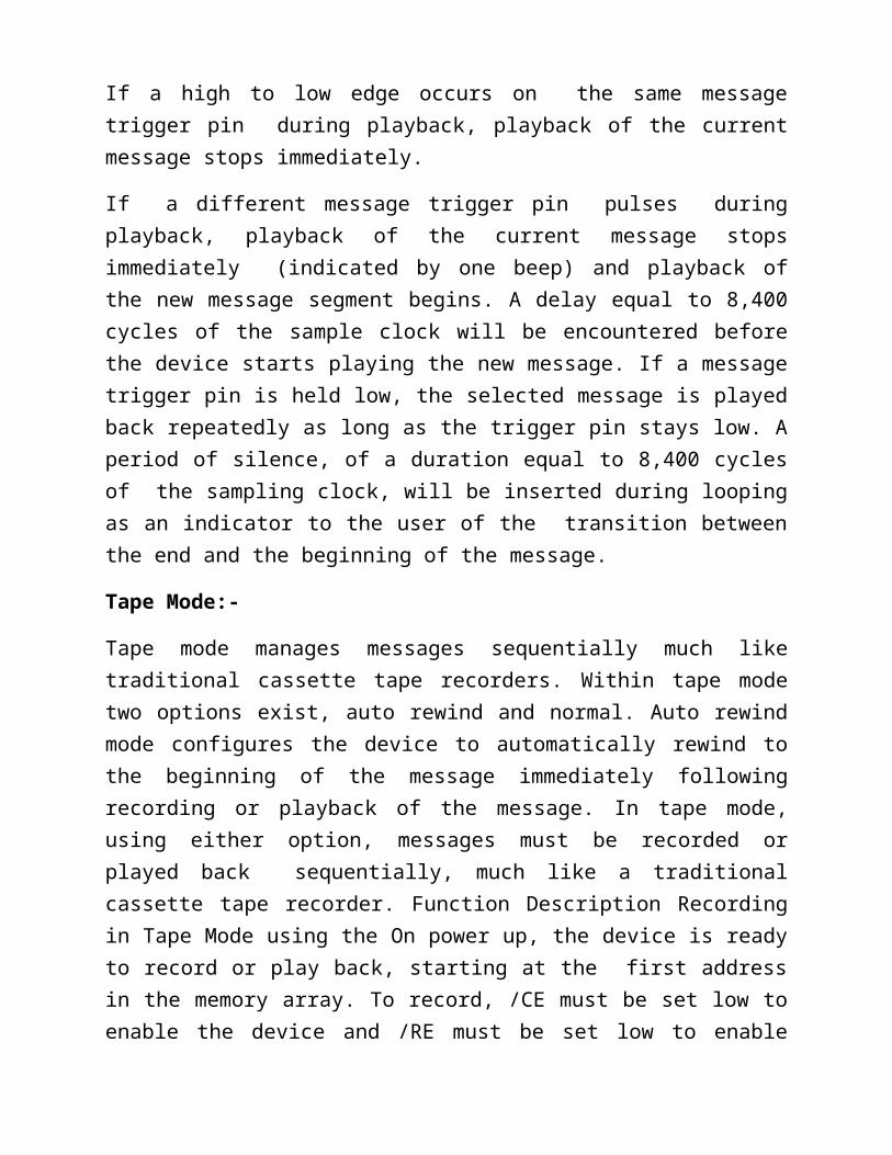
If a different message trigger pin pulses during playback, playback of the current message stops immediately (indicated by one beep) and playback of the new message segment begins. A delay equal to 8,400 cycles of the sample clock will be encountered before the device starts playing the new message. If a message trigger pin is held low, the selected message is played back repeatedly as long as the trigger pin stays low. A period of silence, of a duration equal to 8,400 cycles of the sampling clock, will be inserted during looping as an indicator to the user of the transition between the end and the beginning of the message.
Tape Mode:-
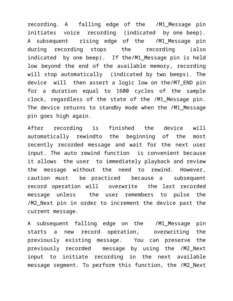
Tape mode manages messages sequentially much like traditional cassette tape recorders. Within tape mode two options exist, auto rewind and normal. Auto rewind mode configures the device to automatically rewind to the beginning of the message immediately following recording or playback of the message. In tape mode, using either option, messages must be recorded or played back sequentially, much like a traditional cassette tape recorder. Function Description Recording in Tape Mode using the On power up, the device is ready to record or play back, starting at the first address in the memory array. To record, /CE must be set low to enable the device and /RE must be set low to enable recording. A falling edge of the /M1_Message pin initiates voice recording (indicated by one beep). A subsequent rising edge of the /M1_Message pin during recording stops the
recording (also indicated by one beep). If the/M1_Message pin is held low beyond the end of the available memory, recording will stop automatically (indicated by two beeps). The device will then assert a logic low on the/M7_END pin for a duration equal to 1600 cycles of the sample clock, regardless of the state of the /M1_Message pin. The device returns to standby mode when the /M1_Message pin goes high again.
After recording is finished the device will automatically rewindto the beginning of the most recently recorded message and wait for the next user input. The auto rewind function is convenient because it allows the user to immediately playback and review the message without the need to rewind. However, caution must be practiced because a subsequent record operation will overwrite the last recorded message unless the user remembers to pulse the /M2_Next pin in order to increment the device past the current message.
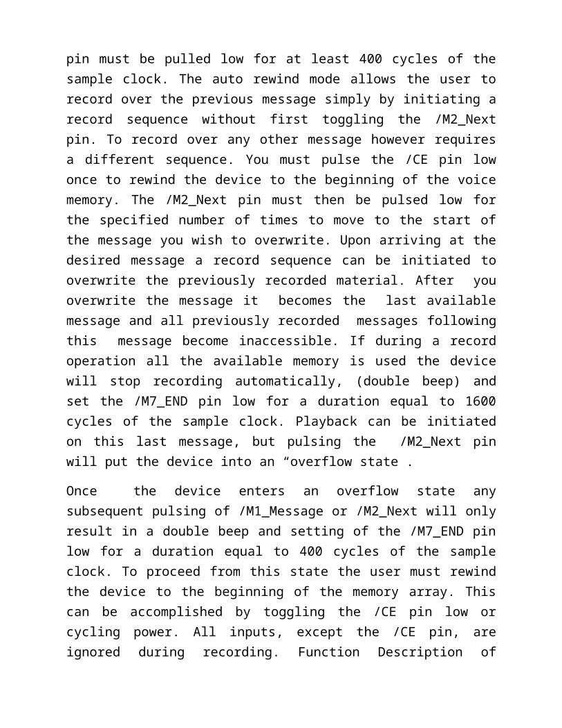
A subsequent falling edge on the /M1_Message pin starts a new record operation, overwriting the previously existing message. You can preserve the previously recorded message by using the /M2_Next input to initiate recording in the next available message segment. To perform this function, the /M2_Next pin must be pulled low for at least 400 cycles of the sample clock. The auto rewind mode allows the user to record over the previous message simply by initiating a record sequence without first toggling the /M2_Next pin. To record over any other message however requires a different sequence. You must pulse the /CE pin low once to rewind the device to the beginning of the voice memory. The /M2_Next pin must then be pulsed low for the specified number of times to move to the start of the message you wish to overwrite. Upon arriving at the desired message a record sequence can be initiated to overwrite the previously recorded material. After you overwrite the message it becomes the last available message and all previously recorded messages following this message become inaccessible. If during a record operation all the available memory is used the device will stop recording automatically, (double beep) and set the /M7_END pin low for a duration equal to 1600 cycles of the sample clock. Playback can be initiated on this last message, but pulsing the /M2_Next pin will put the device into an “overflow state”.
Once the device enters an overflow state any subsequent pulsing of /M1_Message or /M2_Next will only result in a double beep and setting of the /M7_END pin
low for a duration equal to 400 cycles of the sample clock. To proceed from this state the user must rewind the device to the beginning of the memory array. This can be accomplished by toggling the /CE pin low or cycling power. All inputs, except the /CE pin, are ignored during recording. Function Description of Playback in Tape Mode using On power-up, the device is ready to record or play back, starting at the first address in the memory array. Before you can begin playback, the /CE input must be set to low to enable the device and /RE must be set to high to disable recording and enable playback. The first high to low going pulse of the /M1_Message pin initiates playback from the beginning of the current message; on power up the first message is the current message. When the /M1_Message pin pulses low the second time, playback of the current message stops immediately. When the /M1_Message pin pulses low a third time, playback of the current message starts again from its beginning. If you hold the /M1_Message pin low continuously the same message will play continuously in a looping fashion. A 1,530 ms period of silence is inserted during looping as an indicator to the user of the transition between the beginning and end of the message.
Note that in auto rewind mode the device always rewinds to the beginning of the current message. To listen to a subsequent message the device must be fast forwarded past the current message to the next message. This function is accomplished by toggling the /M2_Next pin from high to low.The pulse must be low for least 400 cycles of the sampling clock. After the device is incremented to the desired message the user can initiate playback of the message with the playback sequence described above. A special case exists when the /M2_Next pin goes low during playback. Playback of the current message will stop, the device will beep, advance to the next message and initiate playback of the next message.(Note that if /M2_Next goes low when not in playback mode, the device will prepare to play the next message, but will not actually initiate playback). If the /CE pin goes low during playback, playback of the current message will stop, the device will beep, reset to the beginning of the first message, and wait for a subsequent playback command. When you reach the end of the memory array, any subsequent pulsing of /M1_Message or /M2_Next will only result in a double beep. To proceed from this state the user must rewind the device to the beginning of the memory array. This can be accomplished by toggling the /CE pin low or cycling power.

Functional Description of Recording in Tape Mode using The Normal Option:-
On power-up, the device is ready to record or play back, starting at the first address in the memory array. Before you can begin recording, the /CE input must be set to low to enable the device and /RE must be set to low to enable recording. On a falling edge of the /M1_Message pin the device will beep once and initiate recording. A subsequent rising edge on the /M1_Message pin will stop recording and insert a single beep. If the /M1_Message pin is held low beyond the end of the available memory, recording stops automatically, and two beeps are inserted; regardless of the state of the /M1_Message pin. The device returns to the standby mode when the /M1_Message pin is returned high. A subsequent falling edge on the /M1_Message pin starts a new record operation in the memory array immediately following the last recorded message, thus preserving the last recorded message. To record over all previous messages you must pulse the /CE pin low once to reset the device to the beginning of the first message. You can then initiate a record sequence, as described above, to record a new message. The most recently recorded message will become the last recorded message and all previously recorded messages following this message will become inaccessible. If you wish to preserve any current messages it is recommend that Auto Rewind option be used instead of Normal option. If Normal option is necessary the following sequence can be used. To preserve current messages you must fast forward past the messages you want to keep before you can record a new message. To fast forward when using the Normal option you must switch to play mode and listen to messages sequentially until you arrive at the beginning of the message you wish to overwrite. At this stage you should switch back to record mode and overwrite the desired message. The most recently recorded message will become the last recorded message and all previously recorded messages following this message will become inaccessible. All inputs, except /CE are ignored during recording.
Functional Description of Playback in Tape Mode using Auto Rewind Option:-
On power-up, or after a low to high transition on /RE the device is ready to record or play back starting at the first address in the memory array. Before you can begin playback of messages, the /CE input must be set to low to enable the device and /RE must be set to high to enable playback. The first high to low going pulse of the /M1_Message pin initiates playback from the beginning of the current message. When the /M1_Message pin pulses from high to low a second time, playback of the current message stops immediately. When the /M1_Message pin pulses from high to low a third time, playback of the next message starts again from the beginning. If you hold the /M1_Message pin low continuously, the current message and subsequent messages play until the one of the following conditions is met: the end of the memory array is reached, the last message is reached, the /M1_message pin is released. If the last recorded message has already played, any further transitions on the /M1_Message pin will initiate a double beep for warning and the /M7_END pin will go low. To exit this state you must pulse the /CE pin low once during standby to reset the pointer to the beginning of the first message.
DTMF
Conventionally, Wireless security system used RF technology operated with remote control which have the drawbacks of limited working range limited frequency range and limited control. Here by using mobile phone for operating a device controller cum security system, we can overcome these limitations. It provides the advantages of robust controls working range as large as the coverage area of the service provider which was previously restricted to a small area, no interference with other controllers as no interference problem occurs in mobile communication and up to twelve controls as twelve keys are provided on the keypad of the cell.
This system is controlled by a mobile phone that makes a call to the mobile phone attached to the system i.e. here in this system we are using two mobile phone. One acting as transmitter and the other as receiver. In the course of a call, if any button is pressed a tone corresponding to the button pressed is heard at the other end of the call. This tone is called dual tone multiple frequencies (DTMF) tone. The frequency of the tone received is recorded by the DTMF decoder. This decoder’s output after been further decoded by the digital decoder is fed to the various loads to be secured. Hence the various leads connected to the system can be operated by the mobile phone acting as transmitter.
In order to secure the load, one need to make a call to the cell phone attached to the system (through head phone) from any phone, which sends DTMF tones on pressing the numeric buttons. The cell phone attached to the device controller cum device controller cum security system is kept in ‘auto answer’ mode. As one call from the transmitter or the remote mobile to the stationary mobile within 5 seconds the call is received by the stationary mobile.
Now one may press any button on their mobile to perform any action listed in the table. The four bit output from the DTMF decoder is fed to the HEX inverter IC which inverse the output and then fed to the digital decoder. Here a 4: 16 decoder is used here to give sixteen possible outputs. One of the outputs of the decoder would be selected at a time depending upon the input status.
The output of the decoder is directed toward the NOT gate to make the output active high. Its output is fed to D Flip Flop whose output is connected to the relay

section.This system has a major advantage of large coverage area as compared to the other system as its range extend up to the range of service provider companies like Airtel, Vodafone, reliance, etc.
Application of this system can be found in Vehicle anti theft system, Agriculture sectors , Homes, laboratories, Industries, School / Colleges, Malls, Hotel, Airport, etc. The DTMF stands for Dual Tone Multiple frequency. The DTMF application is associated with digital telephony, and provides two selected output frequency for 100ms duration. The timing in this DTMF subroutine is based on 20MHz clock. The matrix for selecting high and low band frequencies are associated with each key. Each key is uniquely referenced by selecting one of the four low band frequencies associated with the matrix row, coupled with selecting one of four high band frequencies associated with the matrix columns. The low band frequencies are 697,770,852 and 941 Hz, while the high band frequencies are 1209, 1336, 1477 and 1633 Hz. The DTMF subroutine assumes that the key decoding is supplied as a low order hex digit in accumulator. DTMF subroutine will then generate selected high band and low band frequencies on port G output pins G3 and G2 respectively for duration of 100ms
The theory of operation in producing the selecting low band frequencies starts with loading the three counters with values obtained from a ROM table. The half period for the selected frequency is counted out, after which the G2output bit is toggled. During this half period count out, the quotient counter is decremented. This procedure is repeated until the quotient counter counts out, after which the program branches to the remainder loop. During the remainder loop the remainder counter counts out to terminatethe100msFollowing the remainder count out, the G2 and G3 bits are both reset, after which the DTMF subroutine is exited. Greasier must be taken in time balancing the half period loop for the selected low band frequency. Furthermore, the toggling of the G2 output bit (achieved with either a set or reset bi instruction) must also be exactly time balanced to maintain the half period time integrity. Local stall loops (consisting of a DRSZ instruction followed by a JP jump back to the DRSZ for a two byte, six instruction cycle loop) are embedded in both the half period and remainder loops. Consequently, the ROM table parameters for the half period and remained counters are approximately only one sixth of what otherwise might be expected. The program for the half period loop along with the detailed time balancing of the loop for each of the low band frequencies. The DTMF subroutine makes use of two 16
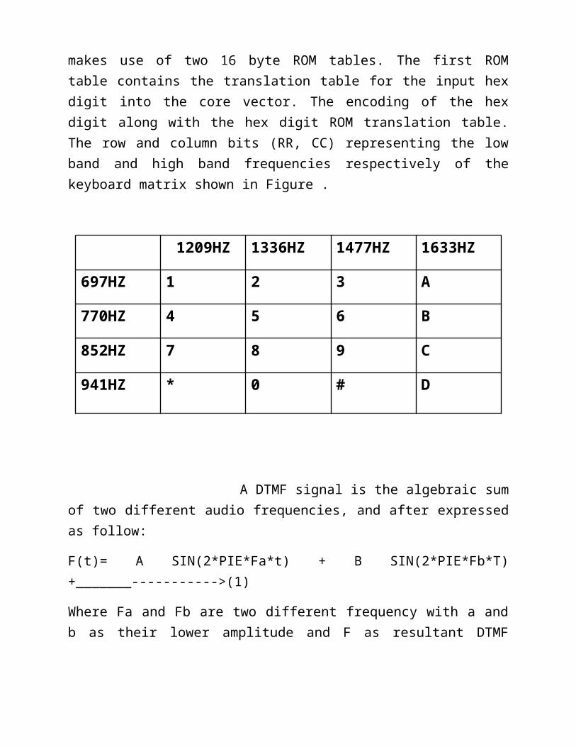
byte ROM tables. The first ROM table contains the translation table for the input hex digit into the core vector. The encoding of the hex digit along with the hex digit ROM translation table. The row and column bits (RR, CC) representing the low band and high band frequencies respectively of the keyboard matrix shown in Figure .
1209HZ 1336HZ 1477HZ 1633HZ
697HZ 1 2 3 A
770HZ 4 5 6 B
852HZ 7 8 9 C
941HZ * 0 # D
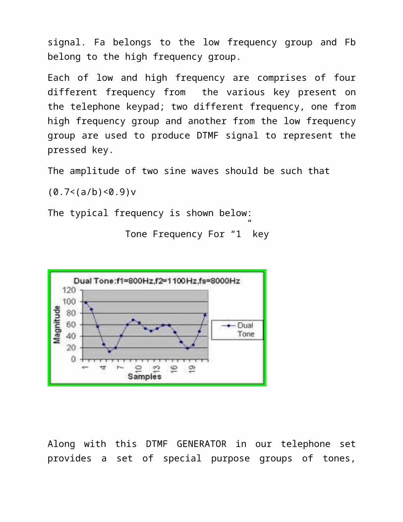
A DTMF signal is the algebraic sum of two different audio frequencies, and after expressed as follow:
F(t)= A SIN(2*PIE*Fa*t) + B SIN(2*PIE*Fb*T)+_______----------->(1)
Where Fa and Fb are two different frequency with a and b as their lower amplitude and F as resultant DTMF signal. Fa belongs to the low frequency group and Fb belong to the high frequency group.
Each of low and high frequency are comprises of four different frequency from the various key present on the telephone keypad; two different frequency, one from high frequency group and another from the low frequency group are used to produce DTMF signal to represent the pressed key.
The amplitude of two sine waves should be such that
(0.7<(a/b)<0.9)v
The typical frequency is shown below:
Tone Frequency For “1” key
Along with this DTMF GENERATOR in our telephone set provides a set of special purpose groups of tones, which are normally not used in our keypad. These tones are identical as ‘A’, ’B’, ‘C’, ‘D’. These frequency have the same column frequency but uses row frequency given in the table in fig(a).The tone are used for communication signaling.
LCD
LCDs with a small number of segments, such as those used in digital watches and pocket calculators, have individual electrical contacts for each segment. An external dedicated circuit supplies an electric charge to control each segment. This display structure is unwieldy for more than a few display elements.
Small monochrome displays such as those found in personal organizers, electronic weighing scales, older laptop screens, and the original Nintendo Game Boy have a passive-matrix structure employing super-twisted nematic (STN)[16] or double-layer STN (DSTN) technology (the latter of which addresses a colour-shifting problem with the former), and colour-STN (CSTN) in which colour is added by using an internal filter. Each row or column of the display has a single electrical circuit. The pixels are addressed one at a time by row and column addresses. This type of display is called passive-matrix addressed because the pixel must retain its state between refreshes without the benefit of a steady electrical charge. As the number of pixels (and, correspondingly, columns and rows) increases, this type of display becomes less feasible. Very slow response times and poor contrast are typical of passive-matrix addressed LCDs.
Monochrome passive-matrix LCDs were standard in most early laptops (although a few used plasma displays). The commercially unsuccessful Macintosh Portable (released in 1989) was one of the first to use an active-matrix display (though still monochrome), but passive-matrix was the norm until the mid-1990s, when colour active-matrix became standard on all laptops.
High-resolution colour displays such as modern LCD computer monitors and televisions use an active matrix structure. A matrix of thin-film transistors (TFTs) is added to the polarizing and colour filters. Each pixel has its own dedicated transistor, allowing each column line to access one pixel. When a row line is activated, all of the column lines are connected to a row of pixels and the correct voltage is driven onto all of the column lines. The row line is then deactivated and the next row line is activated. All of the row lines are activated in sequence during a refresh operation. Active-matrix addressed displays look "brighter" and "sharper" than passive-matrix addressed displays of the same size, and generally have quicker response times, producing much better images.
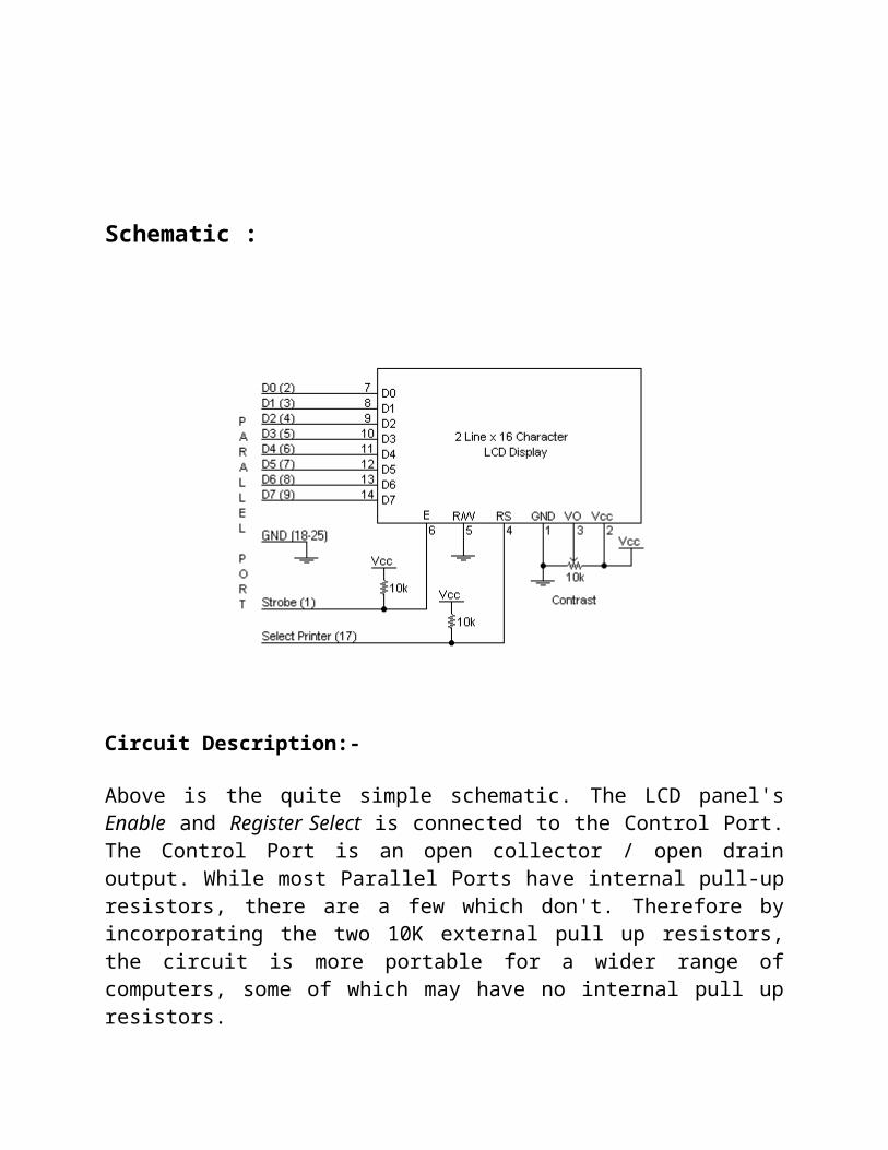
Schematic :
Circuit Description:-
Above is the quite simple schematic. The LCD panel's Enable and Register Select is connected to the Control Port. The Control Port is an open collector / open drain output. While most Parallel Ports have internal pull-up resistors, there are a few which don't. Therefore by incorporating the two 10K external pull up resistors, the circuit is more portable for a wider range of computers, some of which may have no internal pull up resistors.
We make no effort to place the Data bus into reverse direction. Therefore we hard wire the R/W line of the LCD panel, into write mode. This will cause no bus conflicts on the data lines. As a result we cannot read back the LCD's internal Busy Flag which tells us if the LCD has accepted and finished processing the last instruction. This problem is overcome by inserting known delays into our program.
The 10k Potentiometer controls the contrast of the LCD panel. Nothing fancy here. As with all the examples, I've left the power supply out. You can use a bench power supply set to 5v or use a onboard +5 regulator. Remember a few de-coupling capacitors, especially if you have trouble with the circuit working properly.
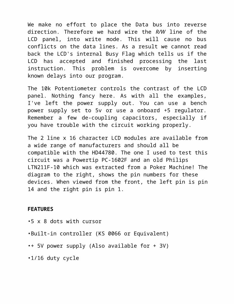
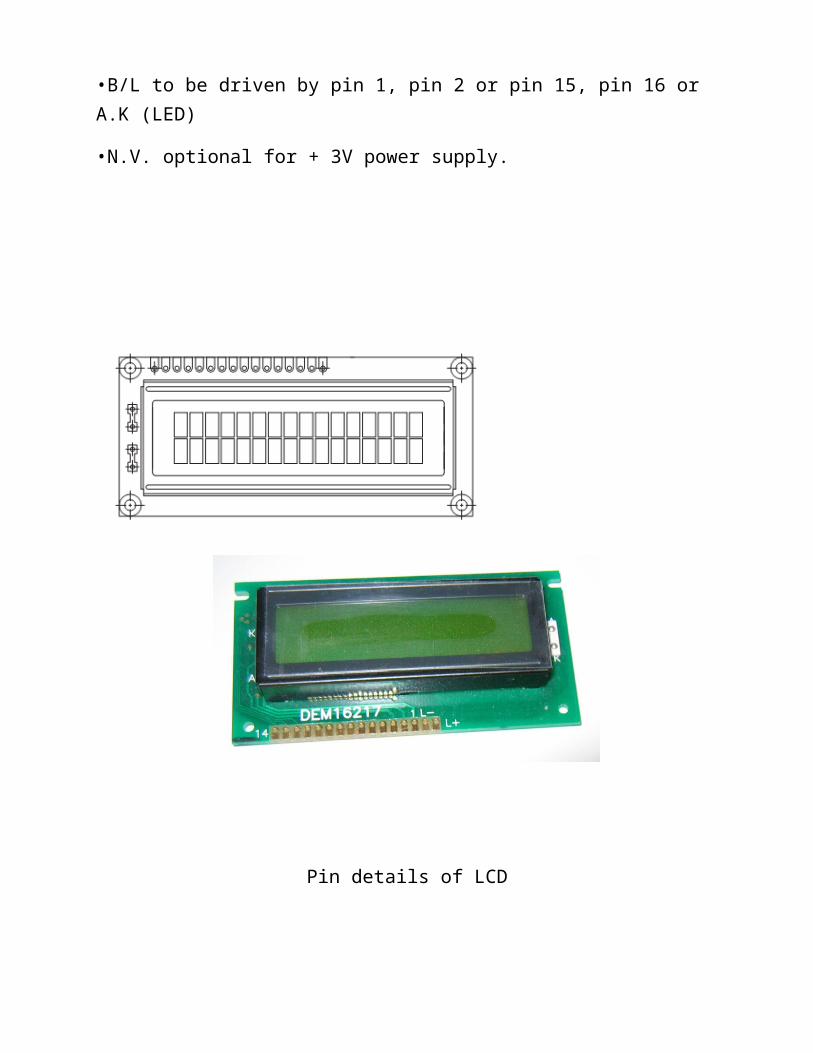
The 2 line x 16 character LCD modules are available from a wide range of
manufacturers and should all be compatible with the HD44780. The one I used to test this circuit was a Powertip PC-1602F and an old Philips LTN211F-10 which was extracted from a Poker Machine! The diagram to the right, shows the pin numbers for these devices. When viewed from the front, the left pin is pin 14 and the right pin is pin 1.
FEATURES
•5 x 8 dots with cursor
•Built-in controller (KS 0066 or Equivalent)
•+ 5V power supply (Also available for + 3V)
•1/16 duty cycle
•B/L to be driven by pin 1, pin 2 or pin 15, pin 16 or A.K (LED)
•N.V. optional for + 3V power supply.
Pin details of LCD
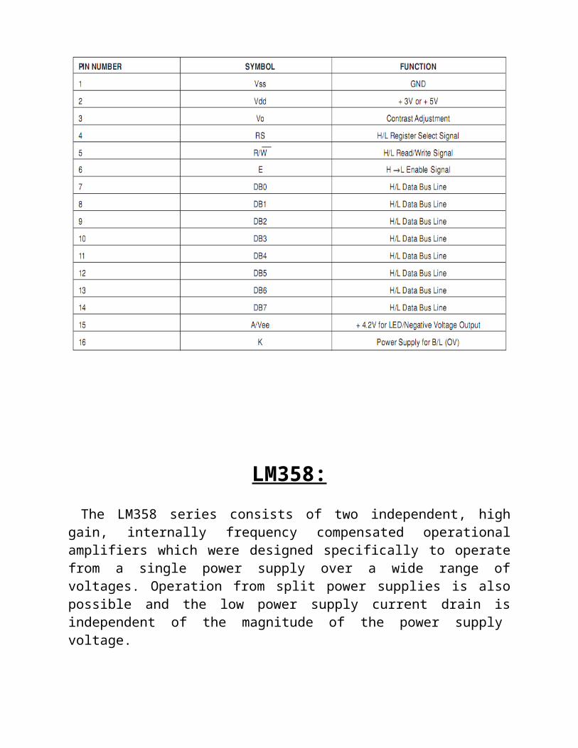
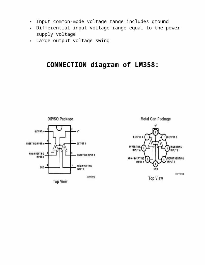
LM358:
The LM358 series consists of two independent, high gain, internally frequency compensated operational amplifiers which were designed specifically to operate from a single power supply over a wide range of voltages. Operation from split power supplies is also possible and the low power supply current drain is independent of the magnitude of the power supply voltage.
Application areas include transducer amplifiers, dc gain blocks and all the conventional op amp circuits which now can be more easily implemented in single power supply systems. For example, the LM158 series can be directly operated off of the standard +5V power supply voltage which is used in digital systems and will easily provide the required interface electronics without requiring the additional ±15V power supplies.
LM 358 Unique Characteristics:-
In the linear mode the input common-mode voltage range includes ground and the output voltage can also swing to ground, even though operated from only a single power supply voltage.
The unity gain cross frequency is temperature compensated. The input bias current is also temperature compensated.
LM358 Features:-
Available in 8-Bump micro SMD chip sized package Internally frequency compensated for unity gain Large dc voltage gain: 100 dB Wide bandwidth (unity gain): 1 MHz (temperature compensated) Wide power supply range: Single supply: 3V to 32V or dual supplies: ±1.5V
to ±16V Very low supply current drain (500 μA)— essentially independent of supply
voltage Low input offset voltage: 2 mV Input common-mode voltage range includes ground Differential input voltage range equal to the power supply voltage Large output voltage swing
CONNECTION diagram of LM358:
Advantages: Two internally compensated op amps Eliminates need for dual supplies Allows direct sensing near GND and VOUT also goes to GND Compatible with all forms of logic Power drain suitable for battery operation
Application:
Application areas include transducer amplifiers, dc gain blocks and all the conventional op amp circuits which now can be more easily implemented in single power supply systems. For example, the LM158 series can be directly operated off of the standard +5V power supply voltage which is used in digital systems and will easily provide the required interface electronics without requiring the additional ±15V power supplies.
ULN2804
ULN2804 is a HIGH-VOLTAGE, HIGH-CURRENT DARLINGTON ARRAYS. The series ULN2801 - 2824 are high voltage, high current darlington arrays each containing eight open collector darlington pairs with common emitters. Each channel is rated at 500mA and can withstand peak currents of 600mA.Suppression diodes are included for inductive load driving and the inputs are pinned opposite the outputs to simplify board layout.These devices are useful for driving a wide range of loads including solenoids, relays DC motors, LED displays, filament lamps and high power buffers.The ULN2801-ULN2824 are supplied in 18 pin plastic DIP packages with a copper leadframe to reduce thermal resistance.
Features:• Eight darlington pais per package• Output current 500 ma per driver (600 ma peak)• Output voltage 50v (uln280x) 95v (uln 282x)• Integral supression diodes for inductive loads• outputs can be paralleled for higher current• TTL/CMOS/PMOS/DTL compatible inputs• Inputs pinned opposite outputs to simplify layout Transient-protected outputs Dual in-line package or wide-body small-outline package

PIN OUT DIAGRAM OF ULN2804
The five versions interface to all common logic families:
ULN2801 General purpose, DTL, TTL, PMOS, CMOS
ULN2802 14-25 V PMOS
ULN2803, ULN2823 5 V TTL, CMOS
ULN2804, ULN2824 6-15 V CMOS, PMOS
These Darlington arrays are furnished in 18-pin dual in-line plastic packages or 18-lead small-outline plastic packages. All devices are pinned with outputs opposite inputs to facilitate ease of circuit board layout. Prefix ‘ULN’ devices are rated for operation over the temperature range of -20°C to +85°C; prefix ‘ULQ’ devices are rated for operation to -40°C.
The ULN2804 is a high voltage, high current Darlington array comprised of eight NPN Darlington pairs. The device features open-collector outputs with suppression Diodes for inductive loads and is ideally suited for interfacing between low-level Logic circuitry and high power loads. Typical loads including relays DC motors, filament lamps, LED Displays printer hammers and high power Buffers
DESCRIPTION
OF
CIRCUIT DIAGRAM
POWER SUPPLY
The +5 volt supply is useful for both analog and digital circuits. DTL, TTL, and
CMOS ICs will all operate nicely from a +5 volt supply. In addition, the +5 volt
supply is useful for circuits that use both analog and digital signals in various
ways. There are many types of power supply. Most are designed to convert high
voltage AC mains electricity to a suitable low voltage supply for electronics
circuits and other devices. A power supply can by broken down into a series of
blocks, each of which performs a particular function
The +5 volt power supply is based on the commercial 7805 voltage regulator IC.
This IC contains all the circuitry needed to accept any input voltage from 8 to 18
volts and produce a steady +5 volt output, accurate to within 5% (0.25 volt). It also
contains current-limiting circuitry and thermal overload protection, so that the IC
won't be damaged in case of excessive load current; it will reduce its output
voltage instead.
The 1000µf capacitor serves as a "reservoir" which maintains a reasonable input
voltage to the 7805 throughout the entire cycle of the ac line voltage. The two
rectifier diodes keep recharging the reservoir capacitor on alternate half-cycles of
the line voltage, and the capacitor is quite capable of sustaining any reasonable
load in between charging pulses.
The 10µf and .01µf capacitors serve to help keep the power supply output voltage
constant when load conditions change. The electrolytic capacitor smoothes out any
long-term or low frequency variations. However, at high frequencies this capacitor
is not very efficient. Therefore, the .01µf is included to bypass high-frequency
changes, such as digital IC switching effects, to ground. The LED and its series
resistor serve as a pilot light to indicate when the power supply is on. I like to use a
miniature LED here, so it will serve that function without being obtrusive or
distracting while I'm performing an experiment. I also use this LED to tell me
when the reservoir capacitor is completely discharged after power is turned off.
Circuit Diagram
FABRICATION METHOD
INTRODUCTION--
Making a Printed Circuit Board is the first step towards building electronic equipment by
any electronic industry. A number of methods are available for making P.C.B., the
simplest method is of drawing pattern on a copper clad board with acid resistant
(etchants) ink or paint or simple nail polish on a copper clad board and do the etching
process for dissolving the rest of copper pattern in acid liquid.
MATERIAL REQUIRED
The apparatus needs for making a P.C.B. is :-
* Copper Clad Sheet
* Nail Polish or Paint
* Ferric Chloride Powder. (Fecl)
* Plastic Tray
* Tap Water etc.
PROCEDURE
The first and foremost in the process is to clean all dirt from copper sheet with say spirit
or trichloro ethylene to remove traces grease or oil etc. and then wash the board under
running tap water. Dry the surface with forced warm air or just leave the board to dry
naturally for some time. Making of the P.C.B. drawing involves some preliminary
consideration such as thickness of lines/ holes according to the components. Now draw
the sketch of P.C.B. design (tracks, rows, square) as per circuit diagram with the help of
nail polish or enamel paint or any other acid resistant liquid. Dry the point surface in open
air, when it is completely dried, the marked holes in P.C.B. may be drilled using 1Mm
drill bits. In case there is any shorting of lines due to spilling of paint, these may be
removed by scraping with a blade or a knife, after the paint has dried.
After drying, 22-30 grams of ferric chloride in 75 ml of water may be heated to
about 60 degree and poured over the P.C.B. , placed with its copper side upwards in a
plastic tray of about 15*20 cm. Stirring the solution helps speedy etching. The dissolution
of unwanted copper would take about 45 minutes. If etching takes longer, the solution
may be heated again and the process repeated. The paint on the pattern can be removed
P.C.B. may then be washed and dried. Put a coat of varnish to retain the shine. Your
P.C.B. is ready.
REACTION
Fecl3 + Cu ----- CuCl3 + Fe
Fecl3 + 3H2O --------- Fe (OH)3 + 3HCL
PRECAUTION
1. Add Ferric Chloride (Fecl3) carefully, without any splashing. Fecl3 is irritating to the
skin and will stain the clothes.
2. Place the board in solution with copper side up.
3. Try not to breathe the vapours. Stir the solution by giving see-saw motion to the dish and
solution in it.
4. Occasionally warm if the solution over a heater-not to boiling. After some time the
unshaded parts change their colour continue to etch. Gradually the base material will
become visible. Etch for two minutes more to get a neat pattern.
5. Don't throw away the remaining Fecl3 solution. It can be used again for next Printed
Circuit Board P.C.B.
SOFTWARE USED
MPLAB:
The latest information on Microchip MPLAB IDE, the Windows® Integrated Development Environment for development systems tools. This list is focused on the MPLAB IDE, MPLAB SIM and MPLAB SIM30 simulators, MPLAB IDE Project Manager and general editing and debugging features.
The MPLAB compiler is a free-standing, optimizing ANSI C compiler for the PIC16 PIC microcontrollers (MCU). The compiler deviates from the ANSI standard X3.159-1989 only where the standard conflicts with efficient PIC MCU support. The compiler is a 32-bit Windows® console application and is fully compatible with Microchip’s MPLAB IDE, allowing source-level debugging with the MPLAB ICE in-circuit emulator, the MPLAB ICD 2 in-circuit debugger or the MPLAB SIM simulator.
The MPLAB C18 compiler has the following features:• ANSI ‘89 compatibility• Integration with the MPLAB IDE for easy-to-use project management andsource-level debugging• Generation of relocatable object modules for enhanced code reuse• Compatibility with object modules generated by the MPASM assembler, allowingcomplete freedom in mixing assembly and C programming in a single project• Transparent read/write access to external memory• Strong support for inline assembly when total control is absolutely necessary• Efficient code generator engine with multi-level optimization• Extensive library support, including PWM, SPI™, I2C™, UART, USART, stringmanipulation and math libraries• Full user-level control over data and code memory allocation
WORKING OF THE PROJECT
Working of Advance Controlling And Monitoring System is explainedSection wise
DTMF SECTION
This section consist of two main components, one is LM-358 which is a signal amplifier and other is MT-8870 which is a DTMF receiver.
When a call is made from the transmitter mobile the receiver phone which is attached to the circuit is kept in auto answering mode. This phone after few seconds automatically attend the call and let the user to do necessary actions. When any key is pressed from the transmitter mobile phone a DTMF tone is generated, this tone can be listened at the receiver phone also which basically act as our signal .When the DTMF tone is received at receiver phone it is fed to the LM358(op-amp based amplifier I.C).This I.C amplifies the input and fed it to MT 8870 .The DTMF signal is decode here and corresponding to that signal a binary data is generated. Each DTMF tone gives a different binary output which can be used to operate and control various devices.
MICROCONTROLLER SECTION
Binary output from the MT8870 acts as input signal for the PIC microcontroller. The signal from transmitter phone reaches here in form of binary data and according to our requirement we can make the use of this signal to operate any device or appliance attached to it. In our project when a key is pressed like if we press 1 then corresponding to that key we have switched ON the appliance or device attached to relay1and so on with 2 and 3 we can operate and switch ON or switch OFF the device according to the programming done. Similarly some keys are fixed for APR I.C also and corresponding to those keys the status of the appliance is checked first and then the recorded message will be played which tells us about the status of appliance whether it is ON or OFF and the speaker attached
to it which is kept near the receiver phone will play the message and it could be listened by us and user can take necessary action.
ACKNOWLEDEMENT SECTION
This section contains APR9600 I.C. It is a re –recordable I.C with playback feature. This I.C is capable of recording a message of 60 second duration. All of it’s input are first kept at highlevel or provided 5volt, when any dtmf signal related to status check reaches the microcontroller then the controller provide 0 volt to that pin of APR in which message related to the status of appliance is stored and that message is played through speaker.
DISPLAY SECTION
This section contains 16x2 L.C.D display which displays each and every information regarding the status of the machine or appliance attached to the circuit whenever they are being operated and keep continuing the same . In our circuit it is attached to PORT B and throughout the process is carried out the L.C.D keep on displaying the message which let the person sitting nearby the display to be informed
RELAY SECTION
This section contains relay driver I.C i.e ULN2804 and relays. When any signal regarding switching ON or OFF is send then corresponding to that signal and the program of controller the device is operated .The controller sends the signal to ULN and the output parallel to its input is switched through relay attached to ULN output and necessary action is performed.
APPENDIX
ANCILLARY COMPONENTS :-
Relay :
Relay is a common, simple application of electromagnetism. It uses an electromagnet made from an iron rod wound with hundreds of fine copper wire. When electricity is applied to the wire, the rod becomes magnetic. A movable contact arm above the rod is then pulled toward the rod until it closes a switch contact. When the electricity is removed, a small spring pulls the contract arm away from the rod until it closes a second switch contact. By means of relay, a current circuit can be broken or closed in one circuit as a result of a current in another circuit.
Relays can have several poles and contacts. The types of contacts could be normally open and normally closed. One closure of the relay can turn on the same normally open contacts; can turn off the other normally closed contacts.
Relay requires a current through their coils, for which a voltage is applied. This voltage for a relay can be D.C. low voltages upto 24V or could be 240V a.c.
A relay is an electrical switch that opens and closes under control of another electrical circuit. In the original form, the switch is operated by an electromagnet to open or close one or many sets of contacts. It was invented by Joseph Henry in 1835. Because a relay is able to control an output circuit of higher power than the input circuit, it can be considered, in a broad sense, to be a form of electrical amplifier.
These contacts can be either Normally Open (NO), Normally Closed (NC), or change-over contacts.
Normally-open contacts connect the circuit when the relay is activated; the circuit is disconnected when the relay is inactive. It is also called Form A contact or "make" contact. Form A contact is ideal for applications that require to switch a high-current power source from a remote device.
Normally-closed contacts disconnect the circuit when the relay is activated; the circuit is connected when the relay is inactive. It is also called Form B contact or "break" contact. Form B contact is ideal for applications that require the circuit to remain closed until the relay is activated.
Change-over contacts control two circuits: one normally-open contact and one normally-closed contact with a common terminal. It is also called Form C contact.
Operation
When a current flows through the coil, the resulting magnetic field attracts an armature that is mechanically linked to a moving contact. The movement either makes or breaks a connection with a fixed contact. When the current to the coil is switched off, the armature is returned by a force that is half as strong as the magnetic force to its relaxed position. Usually this is a spring, but gravity is also used commonly in industrial motor starters. Relays are manufactured to operate quickly. In a low voltage application, this is to reduce noise. In a high voltage or high current application, this is to reduce arcing.If the coil is energized with DC, a diode is frequently installed across the coil, to dissipate the energy from the collapsing magnetic field at deactivation, which would otherwise generate a spike of voltage and might cause damage to circuit components. If the coil is designed to be energized with AC, a small copper ring can be crimped to the end of the solenoid. This "shading ring" creates a small out-of-phase current, which increases the minimum pull on the armature during the AC cycle. [1]
By analogy with the functions of the original electromagnetic device, a solid-state relay is made with a thyristor or other solid-state switching device. To achieve electrical isolation, a light-emitting diode (LED) is used with a photo transistor.
TRANSISTOR :The name is transistor derived from ‘transfer resistors’ indicating a solid
state Semiconductor device. In addition to conductor and insulators, there is a third
class of material that exhibits proportion of both. Under some conditions, it acts as an insulator, and under other conditions it’s a conductor. This phenomenon is called Semi-conducting and allows a variable control over electron flow. So, the transistor is semi conductor device used in electronics for amplitude. Transistor has three terminals, one is the collector, one is the base and other is the emitter, (each lead must be connected in the circuit correctly and only then the transistor will function). Electrons are emitted via one terminal and collected on another terminal, while the third terminal acts as a control element. Each transistor has a number marked on its body. Every number has its own specifications.
There are mainly two types of transistor (i) NPN & (ii) PNP
NPN Transistors:
When a positive voltage is applied to the base, the transistor begins to conduct by allowing current to flow through the collector to emitter circuit. The relatively small current flowing through the base circuit causes a much greater current to pass through the emitter / collector circuit. The phenomenon is called current gain and it is measure in beta.
PNP Transistor:
It also does exactly same thing as above except that it has a negative voltage on its collector and a positive voltage on its emitter.
Transistor is a combination of semi-conductor elements allowing a controlled current flow. Germanium and Silicon is the two semi-conductor elements used for making it. There are two types of transistors such as POINT
CONTACT and JUNCTION TRANSISTORS. Point contact construction is defective so is now out of use. Junction triode transistors are in many respects analogous to triode electron tube.
A junction transistor can function as an amplifier or oscillator as can a triode tube, but has the additional advantage of long life, small size, ruggedness and absence of cathode heating power.
Junction transistors are of two types which can be obtained while manufacturing.
The two types are: -
1) PNP TYPE:This is formed by joining a layer of P type of germanium to an N-P Junction
2) NPN TYPE:This is formed by joining a layer of N type germanium to a P-N Junction.
Both types are shown in figure, with their symbols for representation. The centre section is called the base, one of the outside sections-the emitter and the other outside section-the collector. The direction of the arrowhead gives the direction of the conventional current with the forward bias on the emitter. The conventional flow is opposite in direction to the electron flow.
P N P
N P N
OPERATION OF PNP TRANSISTOR:-
A PNP transistor is made by sand witching two PN germanium or silicon diodes, placed back to back. The centre of N-type portion is extremely thin in comparison to P region. The P region of the left is connected to the positive terminal and N-region to the negative terminal i.e. PN is biased in the forward direction while P region of right is biased negatively i.e. in the reverse direction as shown in Fig. The P region in the forward biased circuit is called the emitter and P region on the right, biased negatively is called collector. The centre is called base.
The majority carriers (holes) of P region (known as emitter) move to N region as they are repelled by the positive terminal of battery while the electrons of N region are attracted by the positive terminal. The holes overcome the barrier and cross the emitter junction into N region. As the width of base region is extremely thin, two to five percent of holes recombine with the free electrons of N-region which result in a small base current while the remaining holes (95% to 98%) reach the collector junction. The collector is biased negatively and the negative collector voltage aids in sweeping the hole into collector region.
RESISTOR:
A resistor is a two-terminal passive electronic component which implements electrical resistance as a circuit element. When a voltage V is applied
across the terminals of a resistor, a current I will flow through the resistor in direct proportion to that voltage. This constant of proportionality is called conductance, G. The reciprocal of the conductance is known as the resistance R, since, with a given voltage V, a larger value of R further "resists" the flow of current I as given by Ohm's law:
Resistors are common elements of electrical networks and electronic circuits and are ubiquitous in most electronic equipment. Practical resistors can be made of various compounds and films, as well as resistance wire (wire made of a high-resistivity alloy, such as nickel-chrome). Resistors are also implemented within integrated circuits, particularly analog devices, and can also be integrated into hybrid and printed circuits.
The electrical functionality of a resistor is specified by its resistance: common commercial resistors are manufactured over a range of more than 9 orders of magnitude. When specifying that resistance in an electronic design, the required precision of the resistance may require attention to the manufacturing tolerance of the chosen resistor, according to its specific application. The temperature
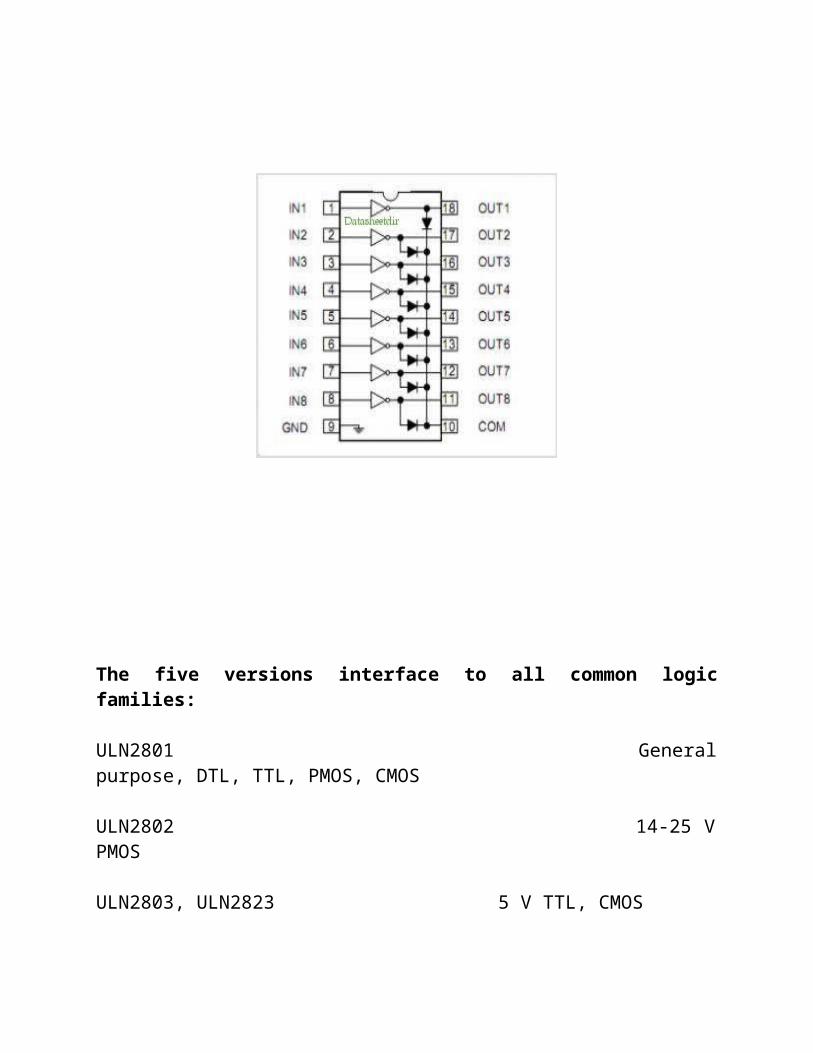
coefficient of the resistance may also be of concern in some precision applications. Practical resistors are also specified as having a maximum power rating which must exceed the anticipated power dissipation of that resistor in a particular circuit: this is mainly of concern in power electronics applications. Resistors with higher power ratings are physically larger and may require heat sinking. In a high voltage circuit, attention must sometimes be paid to the rated maximum working voltage of the resistor.
The series inductance of a practical resistor causes its behavior to depart from ohms law; this specification can be important in some high-frequency applications for smaller values of resistance. In a low-noise amplifier or pre-amp the noise characteristics of a resistor may be an issue. The unwanted inductance, excess noise, and temperature coefficient are mainly dependent on the technology used in manufacturing the resistor. They are not normally specified individually for a particular family of resistors manufactured using a particular technology. A family of discrete resistors is also characterized according to its form factor, that is, the size of the device and position of its leads (or terminals) which is relevant in the practical manufacturing of circuits using them.
CAPACITORS :
It is an electronic component whose function is to accumulate charges and then release it.
To understand the concept of capacitance, consider a pair of metal plates which all are placed near to each other without touching. If a battery is connected to these plates the positive pole to one and the negative pole to the other, electrons from the battery will be attracted from the plate connected to the positive terminal of the battery. If the battery is then disconnected, one plate will be left with an excess of electrons, the other with a shortage, and a potential or voltage difference will exists between them. These plates will be acting as capacitors. Capacitors are of two types: - (1) fixed type like ceramic, polyester, electrolytic capacitors-these names refer to the material they are made of aluminium foil. (2) Variable type like gang condenser in radio or trimmer. In fixed type capacitors, it has two leads and its value is written over its body and variable type has three leads. Unit of measurement of a capacitor is farad denoted by the symbol F. It is a very big unit of capacitance. Small unit capacitor are pico-farad denoted by pf (Ipf=1/1000,000,000,000 f) Above all, in case of electrolytic capacitors, it's two terminal are marked as (-) and (+) so check it while using capacitors in the circuit in right direction. Mistake can destroy the capacitor or entire circuit in operational.
Diode :
In electronics, a diode is a two-terminal electronic component that conducts electric current in only one direction. The term usually refers to a semiconductor diode, the most common type today. This is a crystalline piece of semiconductor material connected to two electrical terminals.[1] A vacuum tube diode (now little
used except in some high-power technologies) is a vacuum tube with two electrodes: a plate and a cathode.
The most common function of a diode is to allow an electric current to pass in one direction (called the diode's forward direction), while blocking current in the opposite direction (the reverse direction). Thus, the diode can be thought of as an electronic version of a check valve. This unidirectional behavior is called rectification, and is used to convert alternating current to direct current, and to extract modulation from radio signals in radio receivers.
However, diodes can have more complicated behavior than this simple on-off action. This is due to their complex non-linear electrical characteristics, which can be tailored by varying the construction of their P-N junction. These are exploited in special purpose diodes that perform many different functions. For example, specialized diodes are used to regulate voltage (Zener diodes), to electronically tune radio and TV receivers (varactor diodes), to generate radio frequency oscillations (tunnel diodes), and to produce light (light emitting diodes). Tunnel diodes exhibit negative resistance, which makes them useful in some types of circuits.
Diodes were the first semiconductor electronic devices. The discovery of crystals' rectifying abilities was made by German physicist Ferdinand Braun in 1874. The first semiconductor diodes, called cat's whisker diodes, developed around 1906, were made of mineral crystals such as galena. Today most diodes are made of silicon, but other semiconductors such as germanium are sometimes used.
Symbol of Diode
LED :
A light-emitting diode is a semiconductor light source. LEDs are used as indicator lamps in many devices and are increasingly used for other lighting. Introduced as a practical electronic component in 1962,early LEDs emitted low-
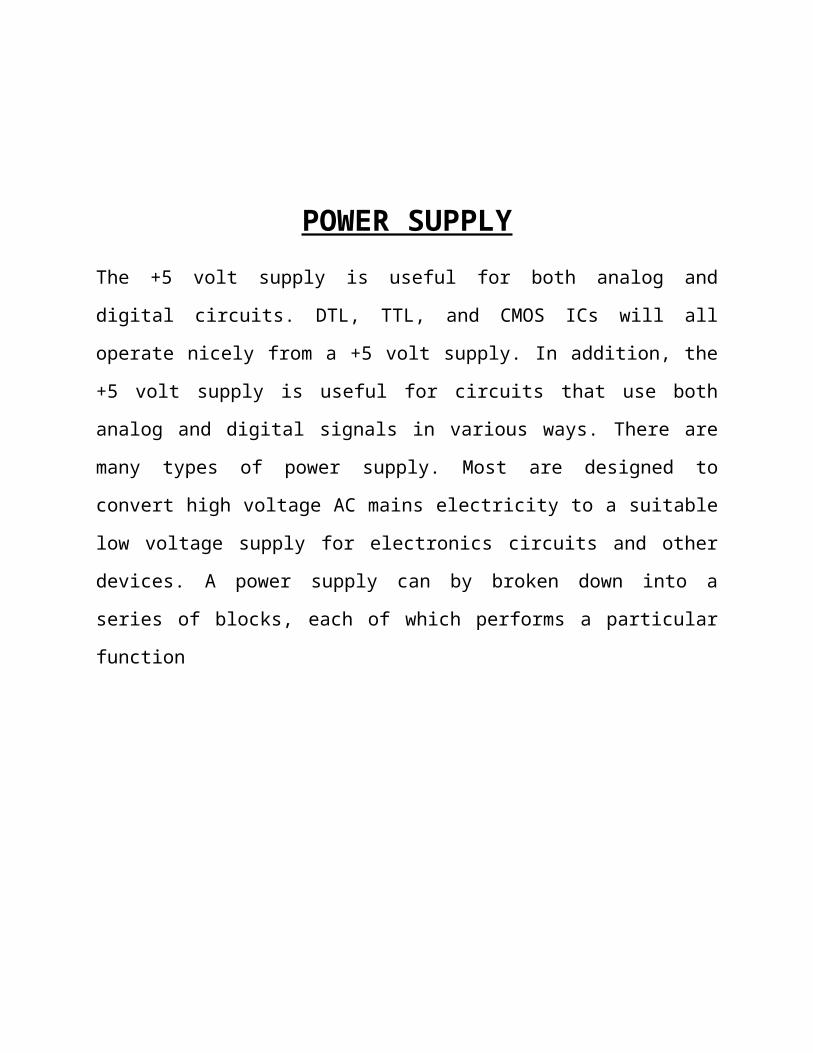
intensity red light, but modern versions are available across the visible, ultraviolet and infrared wavelengths, with very high brightness.
When a light-emitting diode is forward biased (switched on), electrons are able to recombine with electron holes within the device, releasing energy in the form of photons. This effect is called electroluminescence and the color of the light (corresponding to the energy of the photon) is determined by the energy gap of the semiconductor. An LED is often small in area and integrated optical components may be used to shape its radiation pattern.LEDs present many advantages over incandescent light sources including lower energy consumption, longer lifetime, improved robustness, smaller size, faster switching, and greater durability and reliability. LEDs powerful enough for room lighting are relatively expensive and require more precise current and heat management than compact fluorescent lamp sources of comparable output.Light-emitting diodes are used in applications as diverse as replacements for aviation lighting, automotive lighting (particularly brake lamps, turn signals and indicators) as well as in traffic signals. The compact size, the possibility of narrow bandwidth, switching speed, and extreme reliability of LEDs has allowed new text and video displays and sensors to be developed, while their high switching rates are also useful in advanced communications technology. Infrared LEDs are also used in the remote control units of many commercial products including televisions, DVD players, and other domestic appliances.
.
LED
TRANSFORMER
PRINCIPLE:
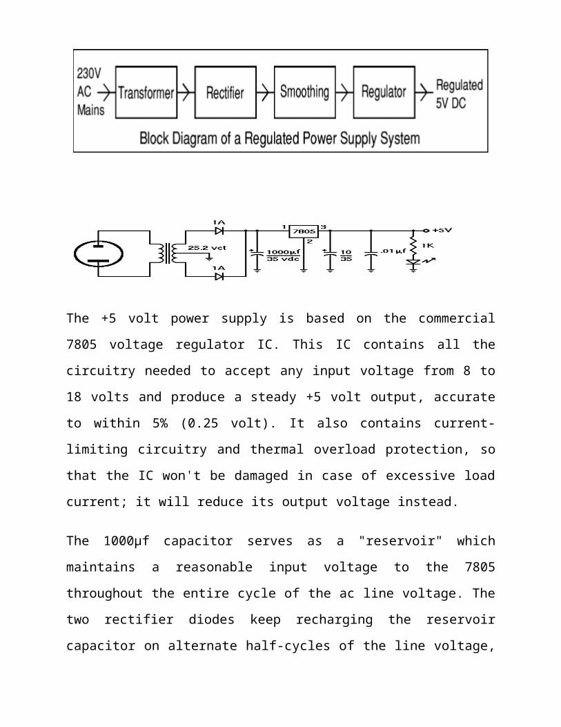
Two coils are wound over a Core such that they are magnetically coupled. The two coils are known as the primary and secondary windings.
In a Transformer, an iron core is used. The coupling between the coils is source of making a path for the magnetic flux to link both the coils. A core as in fig.2 is used and the coils are wound on the limbs of the core. Because of high permeability of iron, the flux path for the flux is only in the iron and hence the flux links both windings. Hence there is very little ‘leakage flux’. This term leakage flux denotes the part of the flux, which does not link both the coils, i.e., when coupling is not perfect. In the high frequency transformers, ferrite core is used. The transformers may be step-up, step-down, frequency matching, sound output, amplifier driver etc. The basic principles of all the transformers are same.
MINIATURE TRANSFORMER CONVENTIONAL POWER TRANSFORMER
VOLTAGE REGULATOR
A voltage regulator is an electrical regulator designed to automatically maintain a constant voltage level. A voltage regulator may be a simple "feed-forward" design or may include negative feedback control loops. It may use an electromechanical mechanism, or electronic components. Depending on the design, it may be used to regulate one or more AC or DC voltages.
Electronic voltage regulators are found in devices such as computer power supplies where they stabilize the DC voltages used by the processor and other elements. In automobile alternators and central power station generator plants, voltage regulators control the output of the plant. In an electric power distribution system, voltage regulators may be installed at a substation or along distribution lines so that all customers receive steady voltage independent of how much power is drawn from the line.
CRYSTAL OSCILLATOR:
Crystal Oscillators are key components used in many electronic circuits, such as in radio frequency applications and digital and microprocessor-

based devices. In order to save power, an ultra low-power oscillator circuit is often desired. In this article we will build 1MHz to 16MHz crystal oscillator circuits and demonstrate a circuit that operates at 7μW with a 4MHz oscillation frequency and operating voltage of +0.3V. An ultra low-power oscillator circuit can be built using recently introduced ultra-low voltage MOSFET arrays. The resulting circuit reduces oscillator power consumption drastically, up to over 100x reduction, and conserves system power for other critical purposes.
The crystal oscillators used in our project are:1. 3.57MHz2. 4MHz
3.57MHz Crystal Oscillator:
Frequency stability is normally specified as a frequency tolerance over a defined operating temperature range with respect to the frequency at reference temperature. The temperature ranges are defined for each crystal in the relevant data sheet. However the majority of crystals will
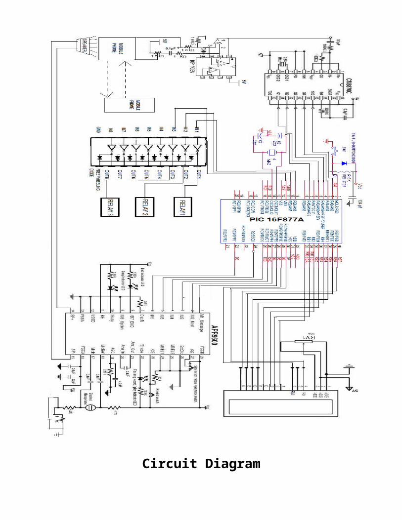
continue to operate quite satisfactorily outside the temperature range for which they are specified, but with a possible degradation of their frequency stability.
4MHZ CRYSTAL OSCILLATOR:
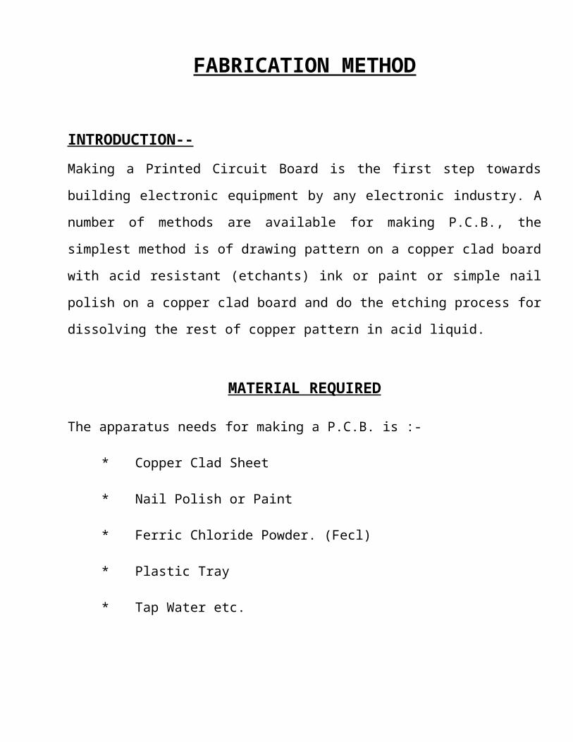
This type of crystal oscillator is used in the microcontroller. A crystal oscillator circuit is built-in between pins T1OSI (input) and T1OSO (amplifier output). It is enabled by setting control bit, T1OSCEN (T1CON<3>). The oscillator is a low power oscillator, rated up to 200 kHz. It will continue to run during SLEEP. It is primarily intendedfor use with a 32 kHz crystal.The capacitor selection for the Timer1 oscillator.
The PIC16F87XA can be operated in four different oscillator modes. The user can program two configuration bits (FOSC1 and FOSC0) to select one of these four modes:
• LP Low Power Crystal• XT Crystal/Resonator• HS High Speed Crystal/Resonator• RC Resistor/Capacitor
CRYSTAL OSCILLATOR/CERAMIC RESONATORS:-
In XT, LP or HS modes, a crystal or ceramic resonator is connected to the OSC1/CLKIN and OSC2/CLKOUT pins to establish oscillation. ThePIC16F87XA oscillator design requires the use of a parallel cut crystal. Use of a series cut crystal may give a frequency out of the crystal manufacturers specifications. When in XT, LP or HS modes, the device can have an external clock source to drive the OSC1/CLKIN pin. MICROPHONE:
The microphone which we are using in our project is ELECTRET Microphone.

An Electret microphone is a type of condenser microphone, which eliminates the need for a polarizing power supply by using a permanently-charged material.
Unlike other condenser microphones, electret types require no polarizing voltage, but they normally contain an integrated preamplifier which does require a small amount of power (often incorrectly called polarizing power or bias). This preamp is frequently phantom powered in sound reinforcement and studio applications. Other types simply include a 1.5V battery in the microphone housing, which is often left permanently connected as the current drain is usually very small.
An electret is a stable dielectric material with a permanently-embedded static electric charge (which, due to the high resistance and chemical stability of the material, will not decay for hundreds of years). The name comes from electrostatic and magnet; drawing analogy to the formation of a magnet by alignment of magnetic domains in a piece of iron. Electrets are commonly made by first melting a suitable dielectric material such as a plastic or wax that contains polar molecules, and then allowing it to re-solidify in a powerful electrostatic field. The polar molecules of the dielectric align themselves to the direction of the electrostatic field, producing a permanent electrostatic "bias". Modern electret microphones use PTFE plastic, either in film or solute form, to form the electret.
There are three major types of electret microphone, differing in the way the electret material is used:
Foil-type or diaphragm-type :
A film of electret material is used as the diaphragm itself. This is the most common type, but also the lowest quality, since the electret material does not make a particularly good diaphragm.
Back electret :
An electret film is applied to the back plate of the microphone capsule and the diaphragm is made of an uncharged material which
may be mechanically more suitable for the transducer design being realized.
Front electret
In this newer type, the back plate is eliminated from the design, and the condenser is formed by the diaphragm and the inside surface of the capsule. The electret film is adhered to the inside front cover and the metalized diaphragm is connected to the input of the FET. It is equivalent to the back electret in that any conductive film may be used for the diaphragm.
Loud speaker:-
A loudspeaker (or "speaker") is an electroacoustic transducer that produces sound in response to an electrical audio signal input.
The term "loudspeaker" may refer to individual transducers (known as "drivers") or to complete speaker systems consisting of an enclosure including one or more drivers. To adequately reproduce a wide range of
frequencies, most loudspeaker systems employ more than one driver, particularly for higher sound pressure level or maximum accuracy. Individual drivers are used to reproduce different frequency ranges. The drivers are named subwoofers (for very low frequencies); woofers (low frequencies); mid-range speakers (middle frequencies); tweeters (high frequencies); and sometimes supertweeters, optimized for the highest audible frequencies. The terms for different speaker drivers differ, depending on the application. In two-way systems there is no mid-range driver, so the task of reproducing the mid-range sounds falls upon the woofer and tweeter. Home stereos use the designation "tweeter" for the high frequency driver, while professional concert systems may designate them as "HF" or "highs". When multiple drivers are used in a system, a "filter network", called a crossover, separates the incoming signal into different frequency ranges and routes them to the appropriate driver. A loudspeaker system with n separate frequency bands is described as "n-way speakers": a two-way system will have a woofer and a tweeter; a three-way system employs a woofer, a mid-range, and a tweeter.
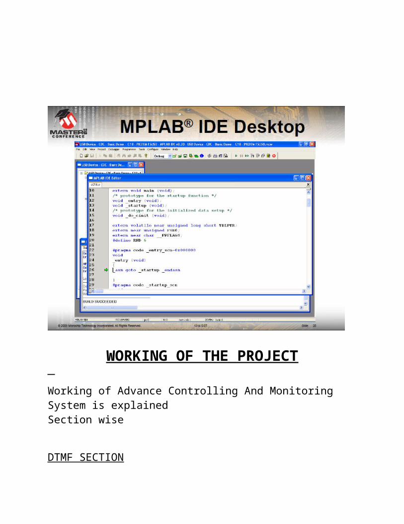
Type of speaker:
1) Full-range speaker2) Subwoofer3) Woofer4) Mid-range speaker5) Tweeter6) Coaxial drivers
A loudspeaker driver that reproduces middle frequencies. Mid-range driver diaphragms can be made of paper or composite materials, and can be direct radiation drivers (rather like smaller woofers) or they can be compression drivers (rather like some tweeter designs). If the mid-range driver is a direct radiator, it can be mounted on the front baffle of a loudspeaker enclosure, or, if a compression driver, mounted at the throat of a horn for added output level and control of radiation pattern.
Most loudspeakers use two wiring points to connect to the source of the signal (for example, to the audio amplifier or receiver). This is usually done using binding posts or spring clips on the back of the enclosure. If the wires for the left and right speakers (in a stereo setup) are not connected "in phase" with each other (the + and − connections on the speaker and amplifier should be connected + to + and − to −), the loudspeakers will be out of polarity. Given identical signals, motion in one cone will be in the opposite direction of the other. This will typically cause monophonic material within a stereo recording to be canceled out, reduced in level, and made more difficult to localize, all due to destructive interference of the sound waves. The cancellation effect is most noticeable at frequencies where the speakers are separated by a quarter wavelength or less; low frequencies.
ADVANTAGES
Easy to access
Multifunctional
Cheaper than other technologies
Long working range
Sound message acknowledgement
Economical
Mobility
small size
low-power consumption
low-cost
possibility to adopt system to new requirements by changing the main program.
Ability to connect the device to personal computer for data storage could be also available.
The device includes the standard and widely spread electrical elements, thus implementing massive production.
APPLICATION
This project can be used in numerous applications.
One of the major applications of this project is in various field of security such as:
Homes Laboratories Vehicle anti-theft system Industries School/college Malls Hotels Hospitals Airport, etc.
Homes devices controller cum security system:-
This project can be used as a home devices controller cum device controller cum security system to secure various gadgets such as lights, T.V system, ovens, A.C etc. A modified version of this project can also be used as a smart phone system.
Industries:-
Various industrial machines can be protected using this system like in NTPC various heavy machine used in process of generating energy can be protected using this system.
School/College:-
Various laboratory equipments are used in colleges can be secured using this system.
Irrigation purpose:-
This system can be useful for irrigation purpose. With the help of this project a farmer can ON the pump and irrigate the farm with water by sitting at home.
Robotics:-
Control of home robots, using if necessary domestic electric beacon.
Home robot communication (i.e. using Wi-Fi) with the domestic network and other home robots.
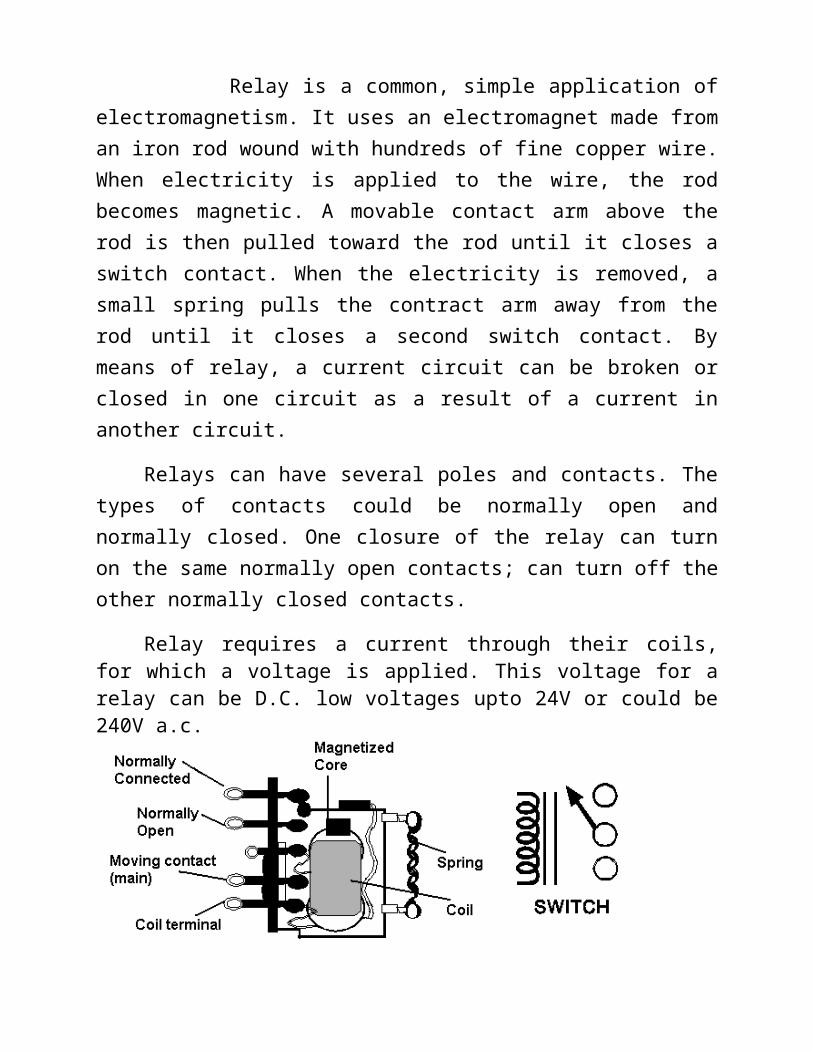
BIBLIOGRAPHY
1) “Mobile communication” BY “Jochen Schiller”.
2) “Electronic devices and circuit” BY “J.B Gupta”.
3) “Electronic devices and circuit” BY “S.K Sahdev”.
4) “Data communication” BY “Wayne Tomasi”.
5) “PIC Microcontroller” BY “Muhammad Ali Mazidi , Rolin McKinlay , Danny Causey” .
6) “Crystal Oscillator Circuits” BY “Robert J. Matthys”.
7) “Wireless Communication” BY “RAPPAPORT”.
8) “ Mikro C PRO for PIC Description” BY “Norbert”.
9) Yun Chan Cho and Jae Wook Jeon, “Remote RobotSystem based on DTMF of Mobile Phone” IEEE International Conference INDIN 2008, July 2008.
10) M J. Callahan, Jr., “Integrated DTMF receiver,” ZEEE J. Solzd-State Czrcuzts, vol. Sc-14, pp. 85-90, Feb.1979.
11) M. Callahan Jr, “Integrated DTMF Receiver,” IEEE Transactions on communications, vol. 27, pp. 343-348, Febrary 1979.
12) R. Sharma, K. Kumar, and S. Viq, “DTMF Based Remote Control System,” IEEE International Conference ICIT 2006, pp. 2380-2383, December 2006.
B001ITRLWW
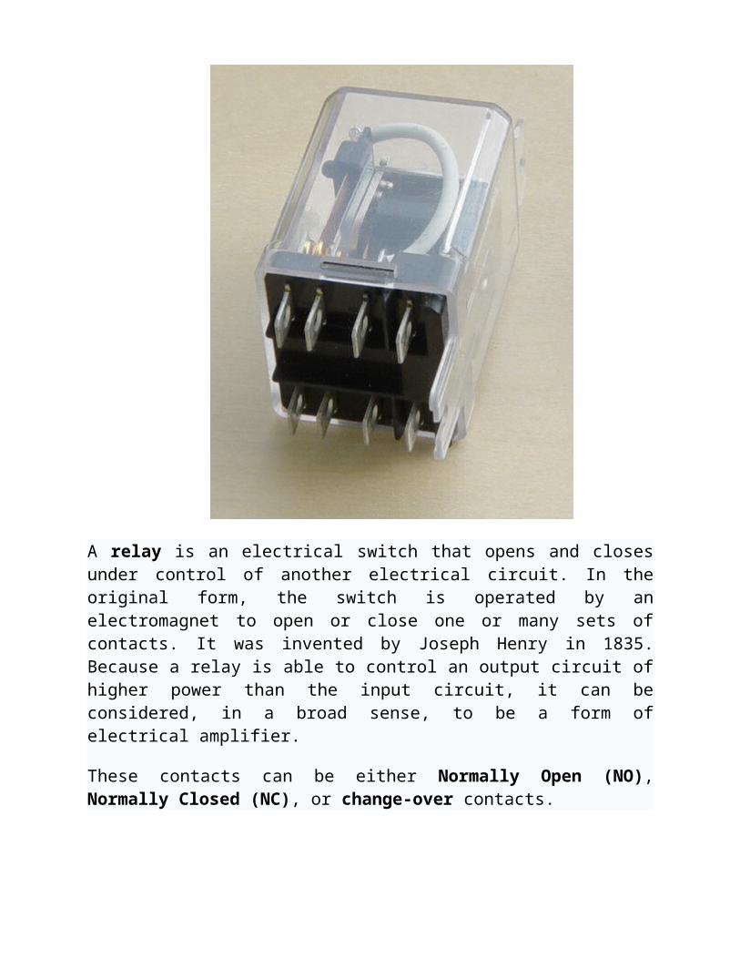
13) Oppenheim, Alan V. and Schafer, Ronald W. Digital Signal Processing. Prentice-Hall of India, 1989.
14) 8870 Datasheet, http://www.clare.com/datasheets/8870-01.pdf
15) Suvad Selman, Raveendran Paramesran,“Comparative Analysis of Methods Used in the Design of DTMF Tone Detectors” IEEE International Conference on Telecommunications and Malaysia International Conference on Communications, 14-17 May 2007, Penang, Malaysia.
16) R.C. Luo, T.M. Chen, and C.C. Yih, “Intelligent autonomous mobile robot control through the Internet,” IEEE International Symposium ISIE 2000, vol. 1, pp. 6-11, December 2000.
17) LPT, http://en.wikipedia.org/wiki/parallelport ICICI-BME 2009 Proceedings
18)
WEBSITE:
www.alldatasheet.com www.wikipedia.org/wiki/Datasheet.com www.datasheetarchive.com www.pdfgeni.com www.pdf-search-engine.com www.microchip.com www.electronics-project-design.com www.electronicspoint.com www.electroniccircuits.com
www.electronics4u.com
www.electronics-lab.com
www.imagesco.com www.electronicsinfoline.com www.electro-tech-online.com www.ieeeusa.org/documents/CAREER/CAREER_LIBRARY/
ethics.html
http://www.smartcomputing.com/editorial/article.asp?article=articles 2F1995 2Fmar95 2Fpcn0323 2Fpcn0323.asp retrieved 2010 09 02
http://drdobbs.com/184404040 Dag Spier, If You Can't Stand the Coding, Stay Out of the Kitchen, "Dr. Dobb's Journal, August 12, 2000
http://www.computer.org/cms/Computer.org/ComputingNow/computingthen/atty/1994/ATTY-1994-2-Echo.pdf James Tomayko "Anecdotes: Electronic Computer for Home Operation, The First Home Computer"
"U.S. Patent 613809: Method of and apparatus for controlling mechanism of moving vessels and vehicles". United States Patent and Trademark Office. 1898-11-08.
http://patft.uspto.gov/netacgi/nph-Parser?Sect1=PTO1&Sect2=HITOFF&d=PALL&p=1&u=/netahtml/PTO/srchnum.htm&r=1&f=G&l=50&s1=0613809.PN.&OS=PN/0613809&RS=PN/0613809. Retrieved 2010-06-16.
William C. Mann (ed.) Smart technology for aging, disability and independence : the state of the science, John Wiley and Sons, 2005 0-471-69694-3, pp. 34-66
http://www.drdobbs.com/184404040;jsessionid=IM5NJPJYWXAOFQE1GHPCKH4ATMY32JVN Dag Spicer, If You Can't Stand the Coding, Stay Out of the Kitchen, Dr. Dobb's Journal, August 2000 , retrieved 2010 Sept 2
"What’s that cable doing?"> "What’s that cable do?". Smartest buildings. http://smartestbuildings.blogspot.com/2010/09/whats-that-cable-do.html. Retrieved 2010-10-29.
"Home automation costs". Totalavcontrol.co.uk. http://www.totalavcontrol.co.uk. Retrieved 2010-02-18.
MAGAZINE:
Electronics for you
Electronic Maker
Electronic Bazar
Everyday Practical Electronics
EE Times
Electronic Design
Embedded System
Test and Measurement
Nuts and Volts
Popular Electronics Magazine
Electronic projects
PHOTO OF PROJECT
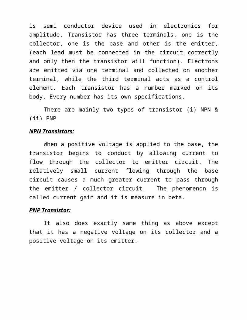
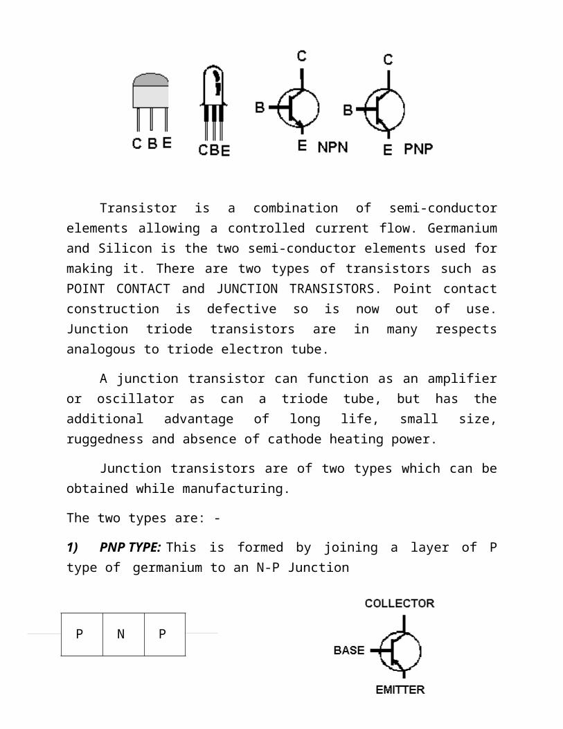
CONCLUSION
This paper presents a method to control a domestic system
using the DTMF tone generated by transmitting telephone instrument
when the user pushes the keypad buttons of the mobile phone connected
to the remote domestic system. This control method uses commercial
mobile communication networks as the path of data transmission. This
enables the user to control the system continuously by sending the
mobile phone DTMF tone. This system is implemented in the 2G mobile
communication network, so video data cannot be obtained.
Home security and home automation system controlled by a cell phone
is possible for any home owner and cell phone user. One of our key
objectives was to engineer a system that would be affordable to every
home owner and not incur a monthly subscription cost. We believe that a
system without a subscription, that is otherwise equal to a modern
security system is a much better value to the average consumer. While
we acknowledge that many similar systems exist, the ability to interface
with the home security system remotely via a phone-line is the most
unique and valuable feature of the system.