actel smartfusion programmable analog user’s guide
TRANSCRIPT

Actel SmartFusion™ ProgrammableAnalog User’s Guide

Actel Corporation, Mountain View, CA 94043© 2010 Actel Corporation. All rights reserved.
Printed in the United States of America
Part Number: 50200251-0
Release: March 2010
No part of this document may be copied or reproduced in any form or by any means without prior written consent of Actel.
Actel makes no warranties with respect to this documentation and disclaims any implied warranties of merchantability or fitness for a particular purpose. Information in this document is subject to change without notice. Actel assumes no responsibility for any errors that may appear in this document.
This document contains confidential proprietary information that is not to be disclosed to any unauthorized person without prior written consent of Actel Corporation.
TrademarksActel, Actel Fusion, IGLOO, Libero, Pigeon Point, ProASIC, SmartFusion and the associated logos are trademarks or registered trademarks of Actel Corporation. All other trademarks and service marks are the property of their respective owners.

SmartFusion Programmable Analog User’s Guide
Table of Contents
SmartFusion Programmable Analog User’s Guide
1 Analog Compute Engine (ACE). . . . . . . . . . . . . . . . . . . . . . . . . . . . . . . . . . . . . . . . . . . . . . . 5ACE Block Diagram . . . . . . . . . . . . . . . . . . . . . . . . . . . . . . . . . . . . . . . . . . . . . . . . . . . . . . . . . . . . . . . . . . . . . . . . . 5Functional Description . . . . . . . . . . . . . . . . . . . . . . . . . . . . . . . . . . . . . . . . . . . . . . . . . . . . . . . . . . . . . . . . . . . . . . 6Interrupts . . . . . . . . . . . . . . . . . . . . . . . . . . . . . . . . . . . . . . . . . . . . . . . . . . . . . . . . . . . . . . . . . . . . . . . . . . . . . . . . 7
2 SmartFusion Analog Front-End (AFE) Overview . . . . . . . . . . . . . . . . . . . . . . . . . . . . . . . . . 9SmartFusion Analog Features . . . . . . . . . . . . . . . . . . . . . . . . . . . . . . . . . . . . . . . . . . . . . . . . . . . . . . . . . . . . . . . . 9SmartFusion Analog Front-End General Description . . . . . . . . . . . . . . . . . . . . . . . . . . . . . . . . . . . . . . . . . . . . . . 9Analog Front-End Configuration . . . . . . . . . . . . . . . . . . . . . . . . . . . . . . . . . . . . . . . . . . . . . . . . . . . . . . . . . . . . . 12Related Information . . . . . . . . . . . . . . . . . . . . . . . . . . . . . . . . . . . . . . . . . . . . . . . . . . . . . . . . . . . . . . . . . . . . . . . 12
3 Analog-to-Digital Converter (ADC) . . . . . . . . . . . . . . . . . . . . . . . . . . . . . . . . . . . . . . . . . . 13Key Features . . . . . . . . . . . . . . . . . . . . . . . . . . . . . . . . . . . . . . . . . . . . . . . . . . . . . . . . . . . . . . . . . . . . . . . . . . . . . 13Block Diagram . . . . . . . . . . . . . . . . . . . . . . . . . . . . . . . . . . . . . . . . . . . . . . . . . . . . . . . . . . . . . . . . . . . . . . . . . . . . 13ADC Theory of Operation . . . . . . . . . . . . . . . . . . . . . . . . . . . . . . . . . . . . . . . . . . . . . . . . . . . . . . . . . . . . . . . . . . 14ADC Terminology . . . . . . . . . . . . . . . . . . . . . . . . . . . . . . . . . . . . . . . . . . . . . . . . . . . . . . . . . . . . . . . . . . . . . . . . . 16SmartFusion ADC Operation . . . . . . . . . . . . . . . . . . . . . . . . . . . . . . . . . . . . . . . . . . . . . . . . . . . . . . . . . . . . . . . . 21ADC Start-Up Sequence . . . . . . . . . . . . . . . . . . . . . . . . . . . . . . . . . . . . . . . . . . . . . . . . . . . . . . . . . . . . . . . . . . . . 27ADC Configuration Example . . . . . . . . . . . . . . . . . . . . . . . . . . . . . . . . . . . . . . . . . . . . . . . . . . . . . . . . . . . . . . . . 28ACE Firmware Driver . . . . . . . . . . . . . . . . . . . . . . . . . . . . . . . . . . . . . . . . . . . . . . . . . . . . . . . . . . . . . . . . . . . . . . 29ADC Register Map . . . . . . . . . . . . . . . . . . . . . . . . . . . . . . . . . . . . . . . . . . . . . . . . . . . . . . . . . . . . . . . . . . . . . . . . 29
4 Sigma-Delta Digital-to-Analog Converter (DAC) . . . . . . . . . . . . . . . . . . . . . . . . . . . . . . . . 35Sigma-Delta DAC (SDD) Features . . . . . . . . . . . . . . . . . . . . . . . . . . . . . . . . . . . . . . . . . . . . . . . . . . . . . . . . . . . . . 35Sigma-Delta DAC General Description . . . . . . . . . . . . . . . . . . . . . . . . . . . . . . . . . . . . . . . . . . . . . . . . . . . . . . . . 35The Sigma-Delta Principle . . . . . . . . . . . . . . . . . . . . . . . . . . . . . . . . . . . . . . . . . . . . . . . . . . . . . . . . . . . . . . . . . . 36Sigma-Delta DAC Detailed Description . . . . . . . . . . . . . . . . . . . . . . . . . . . . . . . . . . . . . . . . . . . . . . . . . . . . . . . . 38Time-Domain and Frequency-Domain Interpretation . . . . . . . . . . . . . . . . . . . . . . . . . . . . . . . . . . . . . . . . . . . . 43Sigma-Delta DAC Configuration . . . . . . . . . . . . . . . . . . . . . . . . . . . . . . . . . . . . . . . . . . . . . . . . . . . . . . . . . . . . . 47Related Information . . . . . . . . . . . . . . . . . . . . . . . . . . . . . . . . . . . . . . . . . . . . . . . . . . . . . . . . . . . . . . . . . . . . . . . 53
5 Active Bipolar Prescaler (ABPS) . . . . . . . . . . . . . . . . . . . . . . . . . . . . . . . . . . . . . . . . . . . . . . 55ABPS Features . . . . . . . . . . . . . . . . . . . . . . . . . . . . . . . . . . . . . . . . . . . . . . . . . . . . . . . . . . . . . . . . . . . . . . . . . . . . 55ABPS General Description . . . . . . . . . . . . . . . . . . . . . . . . . . . . . . . . . . . . . . . . . . . . . . . . . . . . . . . . . . . . . . . . . . 55ABPS Detailed Description . . . . . . . . . . . . . . . . . . . . . . . . . . . . . . . . . . . . . . . . . . . . . . . . . . . . . . . . . . . . . . . . . . 56ABPS Configuration . . . . . . . . . . . . . . . . . . . . . . . . . . . . . . . . . . . . . . . . . . . . . . . . . . . . . . . . . . . . . . . . . . . . . . . 57Related Information . . . . . . . . . . . . . . . . . . . . . . . . . . . . . . . . . . . . . . . . . . . . . . . . . . . . . . . . . . . . . . . . . . . . . . . 58
6 Current Monitor. . . . . . . . . . . . . . . . . . . . . . . . . . . . . . . . . . . . . . . . . . . . . . . . . . . . . . . . . . 59Current Monitor Features . . . . . . . . . . . . . . . . . . . . . . . . . . . . . . . . . . . . . . . . . . . . . . . . . . . . . . . . . . . . . . . . . . 59Current Monitor General Description . . . . . . . . . . . . . . . . . . . . . . . . . . . . . . . . . . . . . . . . . . . . . . . . . . . . . . . . . 59Current Monitor Detailed Description . . . . . . . . . . . . . . . . . . . . . . . . . . . . . . . . . . . . . . . . . . . . . . . . . . . . . . . . 60Current Monitor Configuration . . . . . . . . . . . . . . . . . . . . . . . . . . . . . . . . . . . . . . . . . . . . . . . . . . . . . . . . . . . . . . 64Related Information . . . . . . . . . . . . . . . . . . . . . . . . . . . . . . . . . . . . . . . . . . . . . . . . . . . . . . . . . . . . . . . . . . . . . . . 67
Revision 0

Table of Contents
7 Temperature Monitor . . . . . . . . . . . . . . . . . . . . . . . . . . . . . . . . . . . . . . . . . . . . . . . . . . . . . 69Temperature Monitor Features . . . . . . . . . . . . . . . . . . . . . . . . . . . . . . . . . . . . . . . . . . . . . . . . . . . . . . . . . . . . . . 69Temperature Monitor General Description . . . . . . . . . . . . . . . . . . . . . . . . . . . . . . . . . . . . . . . . . . . . . . . . . . . . 69Temperature Monitor Detailed Description . . . . . . . . . . . . . . . . . . . . . . . . . . . . . . . . . . . . . . . . . . . . . . . . . . . . 70Temperature Monitor Configuration . . . . . . . . . . . . . . . . . . . . . . . . . . . . . . . . . . . . . . . . . . . . . . . . . . . . . . . . . 75Related Information . . . . . . . . . . . . . . . . . . . . . . . . . . . . . . . . . . . . . . . . . . . . . . . . . . . . . . . . . . . . . . . . . . . . . . . 78 . . . . . . . . . . . . . . . . . . . . . . . . . . . . . . . . . . . . . . . . . . . . . . . . . . . . . . . . . . . . . . . . . . . . . . . . . . . . . . . . . . . . . . . . 78
8 High-Speed Comparators . . . . . . . . . . . . . . . . . . . . . . . . . . . . . . . . . . . . . . . . . . . . . . . . . . 79Comparator Features . . . . . . . . . . . . . . . . . . . . . . . . . . . . . . . . . . . . . . . . . . . . . . . . . . . . . . . . . . . . . . . . . . . . . . 79Comparator General Description . . . . . . . . . . . . . . . . . . . . . . . . . . . . . . . . . . . . . . . . . . . . . . . . . . . . . . . . . . . . . 79Comparator Detailed Description . . . . . . . . . . . . . . . . . . . . . . . . . . . . . . . . . . . . . . . . . . . . . . . . . . . . . . . . . . . . 80Comparator Configuration . . . . . . . . . . . . . . . . . . . . . . . . . . . . . . . . . . . . . . . . . . . . . . . . . . . . . . . . . . . . . . . . . 82Comparator Outputs and Interrupts . . . . . . . . . . . . . . . . . . . . . . . . . . . . . . . . . . . . . . . . . . . . . . . . . . . . . . . . . . 85Comparator Application – Using One SDD to Set Multiple Comparator Reference Voltages . . . . . . . . . . . . . 87Related Information . . . . . . . . . . . . . . . . . . . . . . . . . . . . . . . . . . . . . . . . . . . . . . . . . . . . . . . . . . . . . . . . . . . . . . . 89
9 Direct ADC Inputs . . . . . . . . . . . . . . . . . . . . . . . . . . . . . . . . . . . . . . . . . . . . . . . . . . . . . . . . 91Direct ADC Input Features . . . . . . . . . . . . . . . . . . . . . . . . . . . . . . . . . . . . . . . . . . . . . . . . . . . . . . . . . . . . . . . . . . 91Direct ADC Input General Description . . . . . . . . . . . . . . . . . . . . . . . . . . . . . . . . . . . . . . . . . . . . . . . . . . . . . . . . 91Direct ADC Input Detailed Description . . . . . . . . . . . . . . . . . . . . . . . . . . . . . . . . . . . . . . . . . . . . . . . . . . . . . . . . 92Direct ADC Input Configuration . . . . . . . . . . . . . . . . . . . . . . . . . . . . . . . . . . . . . . . . . . . . . . . . . . . . . . . . . . . . . 95Related Information . . . . . . . . . . . . . . . . . . . . . . . . . . . . . . . . . . . . . . . . . . . . . . . . . . . . . . . . . . . . . . . . . . . . . . . 98
A List of Changes. . . . . . . . . . . . . . . . . . . . . . . . . . . . . . . . . . . . . . . . . . . . . . . . . . . . . . . . . . . 99
B Product Support. . . . . . . . . . . . . . . . . . . . . . . . . . . . . . . . . . . . . . . . . . . . . . . . . . . . . . . . . 101Customer Service . . . . . . . . . . . . . . . . . . . . . . . . . . . . . . . . . . . . . . . . . . . . . . . . . . . . . . . . . . . . . . . . . . . . . . . . 101Actel Customer Technical Support Center . . . . . . . . . . . . . . . . . . . . . . . . . . . . . . . . . . . . . . . . . . . . . . . . . . . . 101Actel Technical Support . . . . . . . . . . . . . . . . . . . . . . . . . . . . . . . . . . . . . . . . . . . . . . . . . . . . . . . . . . . . . . . . . . . 101Website . . . . . . . . . . . . . . . . . . . . . . . . . . . . . . . . . . . . . . . . . . . . . . . . . . . . . . . . . . . . . . . . . . . . . . . . . . . . . . . . 101Contacting the Customer Technical Support Center . . . . . . . . . . . . . . . . . . . . . . . . . . . . . . . . . . . . . . . . . . . . 101
Revision 0

1 – Analog Compute Engine (ACE)
The SmartFusion™ analog front-end (AFE) functionality is controlled by the analog computeengine (ACE).
ACE Block Diagram
Figure 1-1 • Analog Compute Engine (A2F500 shown)
3
3
3
AnalogComputeEngine
SRAM512x16
SRAM512x32
Analog Front–End
SampleSequencingEngine
ADC Unit 0SDD
SCB
SCB
An
alo
gM
UX
AD
C
Done
ADC Unit 1SDD
SCB
SCB
An
alo
gM
UX
AD
C
Done
ADC Unit 2SDD
SCB
An
alo
gM
UX
AD
C
Done
PostProcessing
Engine
ACE – APBInterface
FromFPGA Fabric
ToFPGA Fabric
Delay Timer
Delay Timer
Delay TimerNext 0
Next 1
Next 2Mod 2
Mod 1
Mod 0
SampleSequencing
Logic
SSEMix
PPEMix
ConfigRegisters
ConfigRegisters
Sample
Chanel
Sample
Chanel
Sample
Chanel
SampleSequencer
FIFO: 4×16
FIFO: 4×16
FIFO: 4×16
Threshold Flags
PostProcessor
PostProcessing
Logic
APB SlaveInterface
APB Master(Cortex–M3 or FPGA)
InteruptsInterupts
Analog
Config
Trigger
Revision 0 5

Analog Compute Engine (ACE)
Functional DescriptionThe ACE is a small controller that is connected to the AHB bus matrix and communicates with theARM® Cortex™-M3 via interrupts. The behavior of the ACE is set by the user during the designphase. The MSS configurator, found in the Libero® Integrated Design Environment (IDE)SmartDesign design tool, allows configuring the initial stage of all MSS peripherals, including theACE. The user needs to select the ACE configurator within the MSS configurator and create theinitial ACE configuration via the graphical interface provided. In turn, the ACE configuratorautomatically generates the necessary configuration information to program the ACE.
The ACE configurator automatically disables unused sections, based on the user configuration, tosave power. It also creates microcode programs for the sample sequencing engine (SSE) and postprocessing engine (PPE) in the ACE that will cause the ADC to take samples and to apply lineartransformation or calibration based on the factory stored coefficients to each ADC conversions.TheACE configurator provides configuration of various analog services. Each service is a distinct analogfeature that is available in SmartFusion.
You can use the ACE to configure the following services:
• Active bipolar prescaler input – A voltage monitor using the active bipolar prescaler.
• ADC direct input – If input value is less than the ADC reference voltage and high accuracy iscritical for the application.
• Current input – Measures current by sensing the differential voltage across a resistorbetween the CM[n] and TM[n] analog inputs.
• Differential Input – Measures differential voltage between a pair of CM[n] and TM[n]analog inputs.
• Temperature Input – Designed to measure the ambient temperature based on the externaljunction diode.
• LVTTL Input – Using the analog pads as slow digital inputs.
• Analog comparator – An analog comparison of two inputs, or of one input versus areference voltage generated by a DAC
• Sigma-delta DAC – Highly configurable DAC with 8-bit, 16-bit, or 24-bit resolution
Most of the analog channels have similar features, such as digital filtering, linear transformation,and flag threshold settings.
• Digital filtering of the analog input
• Applying a transformation on analog input
• Setting threshold flags on analog input
• How to monitor analog data through the signal processing path
For analog pins that are connected to several analog blocks with mutually exclusive functionality(see the "Analog Front-End Pin-Level Function Multiplexing" section in the SmartFusion IntelligentMixed-Signal FPGAs datasheet), the ACE configurator allows selecting which block is connected toa given pin.
A firmware driver is provided to communicate between the Cortex-M3 and the analog computeengine. The SmartFusion ACE driver provides several sets of functions for controlling the ACE atdifferent levels of abstractions. A set of low-level functions is provided to directly configure andcontrol the ACE without making use of the sample sequencing engine (SSE) or post processingengine (PPE).
A second set of functions allows making full use of the ACE sample sequencing engine (SSE) andpost processing engine (PPE). This mode of operation relies on SSE and PPE microcode having beencreated, using the ACE configurator provided as part of the Libero IDE SmartDesign designenvironment. The SSE will control the sampling sequence of the relevant analog inputs. The PPEwill perform linear transformations, filtering, and threshold flag generation as specified throughthe ACE configurator. This driver is then simply used to read the value of the post processedsamples and react to the threshold flag generated.
6 Revision 0

SmartFusion Programmable Analog User’s Guide
InterruptsThe ACE has access to 85 interrupt sources to communicate with the Cortex-M3. Each interruptsource is selectable within the ACE configurator. All interrupts are XORed and presented to theCortex-M3 as a single interrupt signal. The ACE driver provides the functions necessary to handleinterrupts.
Revision 0 7


2 – SmartFusion Analog Front-End (AFE) Overview
SmartFusion Analog Features• Two or three ADCs per device
• Two or three sigma-delta DACs per device
• Nyquist ADCs are successive approximation type
• ADCs support 8-bit, 10-bit, and 12-bit modes
• Up to 600 KHz sample rate, per ADC
• Each ADC incorporates a sample-and-hold (S&H)
• Simultaneous sampling with multiple ADCs
• Up to twenty-five 0 V–2.56 V unipolar single-ended inputs
• Up to ten bipolar single-ended prescalers
• Active bipolar prescalers have four selectable input ranges: ±2.5 V, ±5.12 V, ±10.24 V, and±15.36 V, with inputs from –11.5 V to +14.4 V
• Up to five differential-input amplifiers with a gain of 50, optimized for use as currentmonitors
• Up to five temperature monitors
• Up to ten high-speed analog comparators with selectable hysteresis
• Up to seven unique analog outputs (from DACs) by use of demultiplexing and S&Htechniques
• DAC sampling rates of over 600 KHz possible
• Built-in precision voltage reference
• External voltage reference input for ratiometric operation of ADC and DAC
• Pins shared between functions for low pin count
SmartFusion Analog Front-End General DescriptionSmartFusion devices have a versatile analog front-end (AFE) that provides a very usefulcomplement to the ARM® Cortex™-M3 microcontroller and general-purpose FPGA fabric.SmartFusion has a sophisticated controller for the analog front-end called the analog computeengine (ACE), which configures and sequences all the analog functions and post-processes theresults, all independently of the Cortex-M3, thus off-loading the Cortex-M3 to perform otherprocessing activities and not either wait idle for data to be sampled or transform the sampled data.
SmartFusion has multiple analog-to-digital converters (ADCs) and digital-to-analog converters(DACs). The A2F200 has two of each, and the A2F500 has three of each.
The SmartFusion ADCs are of the capacitor-ratio successive approximation type. Each self-calibrating ADC has a built-in sample-and-hold (S&H) function for predictable results onceconversion has started. Each 12-bit ADC can be operated in 8-bit or 10-bit mode by prematurelyterminating the conversion, allowing for more conversions to be performed per second. MultipleADCs can simultaneously sample their respective inputs at the same instant, and multipleSmartFusion devices can even be synchronized. Refer to the "Analog-to-Digital Converter (ADC)"section on page 13 for further information.
The SmartFusion DACs are of the one-bit sigma-delta type. The ACE has a built-in first-order sigma-delta modulator which feeds each one-bit DAC. Alternately, each DAC’s input (and clock) can comefrom the FPGA fabric, where a custom modulator can be instantiated. Each DAC includes anon-chip, three-pole, continuous-time low-pass output filter. A fourth pole of potentially muchlower frequency can be added by attaching an external capacitor to the DAC output pin. The DAC
Revision 0 9

SmartFusion Analog Front-End (AFE) Overview
can be operated in either voltage or current output mode. In voltage output mode, a 10 kΩ(nominal) resistor is internally connected to ground.
Many of the analog input functions are organized into signal conditioning blocks (SCBs). Each SCBcontains the following:
• Two active bipolar prescalers (ABPS). These single-ended amplifiers have four selectableinput ranges, and can operate with high input voltages. Refer to the "Active BipolarPrescaler (ABPS)" section on page 55 for further information.
• One high-gain current monitor. These auto-zeroing differential-input amplifiers have a fixedgain of 50, and are optimized for sensing the differential voltage across a current senseresistor, even in the presence of high common mode voltages. Refer to the "CurrentMonitor" section on page 59 for further information.
• One temperature monitor, designed to sense temperature using an external junction diodeor diode-connected bipolar transistor. Refer to the "Temperature Monitor" section onpage 69 for further information.
• Two high-speed analog comparators with selectable hysteresis levels. The reference voltagefor one of each pair can optionally come from any of the SmartFusion DACs, and this signalcan be demultiplexed using internal switches and external (board-level) capacitors as part ofa sample-and-hold circuit. Refer to the "High-Speed Comparators" section on page 79 forfurther information.
Each ADC has four additional direct ADC Inputs. These four inputs can also be configured as LVTTLdigital inputs if they are not needed for their analog functionality, and are available at the fabricinterface for user logic. Refer to the "Fabric Interface and IOMUX" section in the SmartFusionMicrocontroller Subsystem User’s Guide for further information.
Many of the pins of the analog front-end share multiple functions, in order to use as few pins aspossible and thus leave as many as possible for the use of the FPGA and the Cortex-M3 dedicateddigital peripherals. Nearly all the analog blocks contain an enable configuration bit which can beused to save power on any unused functions. There are also other configuration options, such asthe input range selection of the active bipolar prescalers, and the hysteresis selection of thecomparators. The current monitor and the temperature monitor can be disabled and bypassed sotheir input pins go directly to the ADC. Figure 2-1 on page 11 shows the first ADC and DAC, and thefirst two SCBs common to both the A2F200 and A2F500. The A2F200 has exactly twice what isshown in Figure 2-1 on page 11. That is, it has one more ADC, one more DAC, and two more SCBs,exactly as shown—but doubled. All the pin and reference designator numbers increase linearlyfrom the highest value shown in Figure 2-1 on page 11. For example, ABPS[0:3] are shown. Theremaining prescalers in the A2F200 are ABPS[4:7], numbered in the same order as ABPS[0:3] are inFigure 2-1 on page 11. The CM[0:1] pads continue as CM[2:3]. The A2F500 has a third ADC andDAC, with an additional SCB, versus the normal two SCBs per ADC found in the A2F200. The thirdADC still has four additional direct inputs, though two of these do not have a comparator inparallel or a demultiplexer on the DACs, as is the case in all other similar situations.
10 Revision 0

SmartFusion Programmable Analog User’s Guide
Figure 2-1 shows a partial block diagram.
Table 2-1 relates each of the analog front-end functions with the signal conditioning block (SCB) inwhich it is located:
Figure 2-1 • Partial Block Diagram of SmartFusion Programming Analog Showing One ADC, One DAC, and Two SCBs
Partof
SCB0
To/FromFPGA
+ + ––
+ +
+–
––
– –
––
–
++
+
––
To ADCCh. 1
To ADCCh. 2
To ADCCh. 3
To ADCCh. 4
To ADCCh. 8
To ADCCh. 7
To ADCCh. 6
To ADCCh. 5
ABPS0
ABPS0 ABPS3 ABPS2ABPS1 CM0 TM1TM0 CM1
ABPS1 ABPS3 ABPS2
SCB0 GNDTM0 SCB1
CM0 TM0 TM1 CM1
CMP0 CMP2
ADC0
ADC0
ADC2 SDD0
∑Δ-DACSDD0
ADC1 ADC3
To FPGAand ACE
To FPGAand ACE
To/FromACE
FromAce orFPGA
LVTTL[0.3]Digital Inputs
0 21 3
Ch.9
Ch.15
Ch.10
Ch.11
Ch.12
FromOtherDACs
CMP1 CMP3
To FPGAand ACE
To FPGAand ACE
Part ofSCB1
Table 2-1 • Analog Front-End Input Pad Designations and Shared Functions
ADC/ SDD
Signal Conditioning
BlockPad
Name Shared Functions on Pad
ADC0
SDD0
SCB0 CM0 ADC0_CH3 CMP0_P CM0_H
TM0 ADC0_CH4 CMP0_N CM0_L TM0_IO
ABPS0 ADC0_CH1
ABPS1 ADC0_CH2
ADC0 ADC0_CH9 CMP1_P LVTTL0_IN
ADC1 ADC0_CH10 CMP1_N LVTTL1_IN SDDM0_OUT
SCB1 CM1 ADC0_CH7 CMP2_P CM1_H
TM1 ADC0_CH8 CMP2_N CM1_L TM1_IO
ABPS2 ADC0_CH5
ABPS3 ADC0_CH6
ADC2 ADC0_CH11 CMP3_P LVTTL2_IN
ADC3 ADC0_CH12 CMP3_N LVTTL3_IN SDDM1_OUT
(N/A) SDD0 ADC0_CH15 SDD0_OUT
Note: *Components indicated are available only in the A2F500.
Revision 0 11

SmartFusion Analog Front-End (AFE) Overview
Analog Front-End ConfigurationMany of the analog functions are calibrated by Actel during test of the SmartFusion devices. Thesecalibrations are stored in dedicated nonvolatile memory in each part.
The Actel SmartDesign software automatically configures many features of the analog front-end,according to the selections made by the end user using the graphical front-end it provides. Itconfigures static bits, such as enabling used sections and disabling unused sections to save power. Italso creates microcode programs for the sample sequencing engine (SSE) and post processingengine (PPE) in the ACE which will cause the ADC to take samples and to apply the factory-storedcompensation values to the readings. In some cases, user-supplied calibration values are mergedwith the factory-supplied values. This automatically generated program is usually all that isnecessary to use the SmartFusion analog front-end. However, it is possible to dynamically changemost every setting, including dynamically enabling and disabling functions, or sequentially usingan input pin for more than one function by writing custom microcode. Refer to the "AnalogCompute Engine (ACE)" section on page 5 for more information.
Related InformationSmartFusion Intelligent Mixed-Signal FPGAs datasheet
http://www.actel.com/documents/SmartFusion_DS.pdf
ADC1
SDD1
SCB2 CM2 ADC1_CH3 CMP4_P CM2_H
TM2 ADC1_CH4 CMP4_N CM2_L TM2_IO
ABPS4 ADC1_CH1
ABPS5 ADC1_CH2
ADC4 ADC1_CH9 CMP5_P LVTTL4_IN
ADC5 ADC1_CH10 CMP5_N LVTTL5_IN SDDM2_OUT
SCB3 CM3 ADC1_CH7 CMP6_P CM3_H
TM3 ADC1_CH8 CMP6_N CM3_L TM3_IO
ABPS6 ADC1_CH5
ABPS7 ADC1_CH6
ADC6 ADC1_CH11 CMP7_P LVTTL6_IN
ADC7 ADC1_CH12 CMP7_N LVTTL7_IN SDDM3_OUT
(N/A) SDD1 ADC1_CH15 SDD1_OUT
ADC2*
SDD2*
SCB4* CM4* ADC2_CH3* CMP8_P* CM4_H*
TM4* ADC2_CH4* CMP8_N* CM4_L* TM4_IO*
ABPS8* ADC2_CH1*
ABPS9* ADC2_CH2*
ADC8* ADC2_CH9* CMP9_P* LVTTL8_IN*
ADC9* ADC2_CH10* CMP9_N* LVTTL9_IN* SDDM4_OUT*
(N/A) SDD2* ADC2_CH15* SDD2_OUT*
Table 2-1 • Analog Front-End Input Pad Designations and Shared Functions (continued)
ADC/ SDD
Signal Conditioning
BlockPad
Name Shared Functions on Pad
Note: *Components indicated are available only in the A2F500.
12 Revision 0

3 – Analog-to-Digital Converter (ADC)
The Actel SmartFusion™ ADC is a 12-bit successive approximation register (SAR) ADC. Figure 3-1shows a simplified block diagram of the SmartFusion ADC. The A2F200 contains two ADCs and theA2F500 contains three ADCs. Multiple ADCs can be triggered to sample signals simultaneously.
Key Features• Configurable resolution: 8-bit, 10-bit, and 12-bit mode
• Differential nonlinearity (DNL) Error: 0.6 LSB for 10-bit mode
• Integral nonlinearity (INL) Error: 0.8 LSB for 10-bit mode
• Internal VAREF = 2.56 V
• Maximum sample rate = 600 Ksps
• Power-up calibration and dynamic calibration after every sample to compensate fortemperature drift over time
Block DiagramFigure 3-1 shows a simplified block diagram for the ADC.
Figure 3-1 • ADC Simplified Block Diagram
AMUXSEL
SAR ADC
ADCX_STC ADCX_MISC_CTRL
Status
ADCX_TVCADCCLKACLK
From SCBs
VAREF
DataValidBusy
SampleCalibrate
S & HADC_RESULT
12
Revision 0 13

Analog-to-Digital Converter (ADC)
ADC Theory of OperationAn analog-to-digital converter is used to capture discrete samples of a continuous analog voltageand provide a discrete binary representation of the signal. Analog-to-digital converters aregenerally characterized in three ways:
• Input voltage range
• Resolution
• Bandwidth or conversion rate
The input voltage range of an ADC is determined by its reference voltage (VREF). Actel SmartFusiondevices include an internal 2.56 V reference, or the user can supply an external reference of up to3.3 V. The following examples use the internal 2.56 V reference, so the full-scale input range of theADC is 0 to 2.56 V.
The resolution (LSB) of the ADC is a function of the number of binary bits in the converter. The ADCapproximates the value of the input voltage using 2n steps, where n is the number of bits in theconverter. Each step therefore represents VREF / 2n volts. In the case of the SmartFusion ADCconfigured for 12-bit operation, the LSB is 2.56 V / 4096 = 0.625 mV.
Finally, bandwidth is an indication of the maximum number of conversions the ADC can performeach second. The bandwidth of an ADC is constrained by its architecture and several keyperformance characteristics.
There are several popular ADC architectures, each with advantages and limitations. The analog-to-digital converter in SmartFusion devices is a switched-capacitor successive approximation register(SAR) ADC. It supports 8-, 10-, and 12-bit modes of operation with a cumulative sample rate up to600,000 samples per second (Ksps). A built-in bandgap circuitry offers 1% internal voltagereference accuracy or an external reference voltage can be used.
As shown in Figure 3-2, a SAR ADC contains N capacitors with binary-weighted values.
To begin a conversion, all of the capacitors are quickly discharged. Then VIN is applied to all thecapacitors for a period of time (acquisition time) during which the capacitors are charged to a valuevery close to VIN. Then all of the capacitors are switched to ground, and thus –VIN is applied acrossthe comparator. Now the conversion process begins. First, C is switched to VREF. Because of thebinary weighting of the capacitors, the voltage at the input of the comparator is then shown byEQ 3-1.
Voltage at input of comparator = –VIN + VREF / 2
EQ 3-1
If VIN is greater than VREF / 2, the output of the comparator is 1; otherwise, the comparator outputis 0. A register is clocked to retain this value as the MSB of the result. Next, if the MSB is 0, C is
Figure 3-2 • Example SAR ADC Architecture
Comparator
C C / 2 C / 4 C / 2N–2 C / 2N–1
VREFVIN
14 Revision 0

SmartFusion Programmable Analog User’s Guide
switched back to ground; otherwise, it remains connected to VREF, and C / 2 is connected to VREF.The result at the comparator input is now either –VIN + VREF / 4 or –VIN + 3 VREF / 4 (depending onthe state of the MSB), and the comparator output now indicates the value of the next mostsignificant bit. This bit is likewise registered, and the process continues for each subsequent bituntil a conversion is completed. The conversion process requires some acquisition time plus N + 1ADC clock cycles to complete.
This process results in a binary approximation of VIN. Generally, there is a fixed interval T, thesampling period, between the samples. The inverse of the sampling period is often referred to asthe sampling frequency fS = 1 / T. The combined effect is illustrated in Figure 3-3.
Figure 3-3 demonstrates that if the signal changes faster than the sampling rate can accommodate,or if the actual value of VIN falls between counts in the result, this information is lost during theconversion. There are several techniques that can be used to address these issues.
First, the sampling rate must be chosen to provide enough samples to adequately represent theinput signal. Based on the Nyquist-Shannon Sampling Theorem, the minimum sampling rate mustbe at least twice the frequency of the highest frequency component in the target signal (NyquistFrequency). For example, to recreate the frequency content of an audio signal with up to 22 KHzbandwidth, the user must sample it at a minimum of 44 ksps. However, as shown in Figure 3-3,significant post-processing of the data is required to interpolate the value of the waveform duringthe time between each sample.
Similarly, to re-create the amplitude variation of a signal, the signal must be sampled withadequate resolution. Continuing with the audio example, the dynamic range of the human ear(the ratio of the amplitude of the threshold of hearing to the threshold of pain) is generallyaccepted to be 135 dB, and the dynamic range of a typical symphony orchestra performance isaround 85 dB. Most commercial recording media provide about 96 dB of dynamic range using 16-bit sample resolution. But 16-bit fidelity does not necessarily mean that you need a 16-bit ADC. Aslong as the input is sampled at or above the Nyquist Frequency, post-processing techniques can beused to interpolate intermediate values and reconstruct the original input signal to within desiredtolerances.
If sophisticated digital signal processing (DSP) capabilities are available, the best results areobtained by implementing a reconstruction filter, which is used to interpolate many intermediatevalues with higher resolution than the original data. Interpolating many intermediate valuesincreases the effective number of samples, and higher resolution increases the effective number ofbits in the sample. In many cases, however, it is not cost-effective or necessary to implement such asophisticated reconstruction algorithm. For applications that do not require extremely finereproduction of the input signal, alternative methods can enhance digital sampling results withrelatively simple post-processing. The details of such techniques are out of the scope of thischapter; refer to the Improving ADC Results through Oversampling and Post-Processing of Datawhite paper for more information.
Figure 3-3 • Conversion Example
T
LSB
Revision 0 15

Analog-to-Digital Converter (ADC)
ADC Terminology
Conversion TimeConversion time is the interval between the release of the hold state (imposed by the inputcircuitry of a track-and-hold) and the instant at which the voltage on the sampling capacitor settlesto within one LSB of a new input value.
DNL – Differential Non-Linearity For an ideal ADC, the analog-input levels that trigger any two successive output codes should differby one LSB (DNL = 0). Any deviation from one LSB in defined as DNL (Figure 3-4).
ENOB – Effective Number of BitsENOB specifies the dynamic performance of an ADC at a specific input frequency and samplingrate. An ideal ADC’s error consists only of quantization of noise. As the input frequency increases,the overall noise (particularly in the distortion components) also increases, thereby reducing theENOB and SINAD (also see "SINAD – Signal-to-Noise and Distortion" on page 19). ENOB for a full-scale, sinusoidal input waveform is computed using EQ 3-2.
EQ 3-2
FS Error – Full-Scale ErrorFull-scale error is the difference between the actual value that triggers that transition to full-scaleand the ideal analog full-scale transition value. Full-scale error equals offset error plus gain error.
Figure 3-4 • Differential Non-Linearity (DNL)
AD
C O
utp
ut
Co
de
Input V oltage to P rescaler
Error = –0.5 LSB
Error = +1 LSB
Ideal Output
Actual Output
ENOB SINAD 1.76–6.02
-----------------------------------=
16 Revision 0

SmartFusion Programmable Analog User’s Guide
Gain Error The gain error of an ADC indicates how well the slope of an actual transfer function matches theslope of the ideal transfer function. Gain error is usually expressed in LSB or as a percent of full-scale (%FSR). Gain error is the full-scale error minus the offset error (Figure 3-5).
Gain Error DriftGain-error drift is the variation in gain error due to a change in ambient temperature, typicallyexpressed in ppm/°C.
Figure 3-5 • Gain Error
AD
C O
utp
ut
Co
de
Input V oltage to P rescaler
Ideal Output
Actual Output
Gain = 2 LSB
1...11
0...00
FSV
olt
age
Revision 0 17

Analog-to-Digital Converter (ADC)
INL – Integral Non-LinearityINL is the deviation of an actual transfer function from a straight line. After nullifying offset andgain errors, the straight line is either a best-fit straight line or a line drawn between the end pointsof the transfer function (Figure 3-6).
LSB – Least Significant BitIn a binary number, the LSB is the least weighted bit in the group. Typically, the LSB is the furthestright bit. For an ADC, the weight of an LSB equals the full-scale voltage range of the converterdivided by 2N, where N is the converter’s resolution.
EQ 3-3 shows the calculation for a 10-bit ADC with a unipolar full-scale voltage of 2.56 V:
1 LSB = (2.56 V / 210) = 2.5 mV
EQ 3-3
No Missing CodesAn ADC has no missing codes if it produces all possible digital codes in response to a ramp signalapplied to the analog input.
Offset ErrorOffset error indicates how well the actual transfer function matches the ideal transfer function at asingle point. For an ideal ADC, the first transition occurs at 0.5 LSB above zero. The offset voltage ismeasured by applying an analog input such that the ADC outputs all zeroes and increases until thefirst transition occurs (Figure 3-7 on page 19).
Figure 3-6 • Integral Non-Linearity (INL)
AD
C O
utp
ut
Co
de
Input V oltage to P rescaler
INL = +0.5 LSB
INL = +1 LSB
Ideal Output
Actual Output
18 Revision 0

SmartFusion Programmable Analog User’s Guide
ResolutionADC resolution is the number of bits used to represent an analog input signal. To more accuratelyreplicate the analog signal, resolution needs to be increased.
Sampling RateSampling rate or sample frequency, specified in samples per second (sps), is the rate at which anADC acquires (samples) the analog input.
SNR – Signal-to-Noise RatioSNR is the ratio of the amplitude of the desired signal to the amplitude of the noise signals at agiven point in time. For a waveform perfectly reconstructed from digital samples, the theoreticalmaximum SNR (EQ 3-4) is the ratio of the full-scale analog input (RMS value) to the RMSquantization error (residual error). The ideal, theoretical minimum ADC noise is caused byquantization error only and results directly from the ADC’s resolution (N bits):
EQ 3-4
SINAD – Signal-to-Noise and DistortionSINAD is the ratio of the RMS amplitude to the mean value of the root-sum-square of all the otherspectral components, including harmonics, but excluding DC. SINAD is a good indication of theoverall dynamic performance of an ADC because it includes all components which make up noiseand distortion.
Figure 3-7 • Offset Error
AD
C O
utp
ut
Co
de
Input V oltage to P rescaler
Ideal Output
Offset Error = 1.5 LSB
Actual Output
0...00
0...01
SNRdB[MAX] 6.02dB N 1.76dB+×=
Revision 0 19

Analog-to-Digital Converter (ADC)
Total Harmonic DistortionTHD measures the distortion content of a signal, and is specified in decibels relative to the carrier(dBc). THD is the ratio of the RMS sum of the selected harmonics of the input signal to thefundamental itself. Only harmonics within the Nyquist limit are included in the measurement.
TUE – Total Unadjusted ErrorTUE is a comprehensive specification that includes linearity errors, gain error, and offset error. It isthe worst-case deviation from the ideal device performance. TUE is a static specification(Figure 3-8).
Figure 3-8 • Total Unadjusted Error (TUE)
AD
C O
utp
ut
Co
de
Input V oltage to P rescaler
IDEAL OUTPUT
TUE = ±0.5 LSB
20 Revision 0

SmartFusion Programmable Analog User’s Guide
SmartFusion ADC Operation
Analog MultiplexerThe SmartFusion ADC has a built-in analog multiplexer as shown in Figure 3-1 on page 13. Inputchannels are selected for conversion by setting the AMUXSEL field in the ADCx_CONV_CTRLregister to the channel desired. Table 3-1 lists the channels available for conversion by therespective ADCs. Each ADC multiplexer is individually configurable by the respectiveADCx_CONV_CTRL register.
Acquisition Time or Sample Time ControlAcquisition time (tSAMPLE) specifies how long an analog input signal has to charge the internalcapacitor array. Figure 3-9 shows a simplified internal input sampling mechanism of a SAR ADC.
Table 3-1 • ADC0 and ADC1 Channel Assignments
ADC0 ADC1 ADC2*
AMUXSEL Pad Name AMUXSEL Pad Name AMUXSEL* Pad Name*
0 1.5 V 0 1.5 V 0* 1.5V*
1 ABPS0 1 ABPS4 1* ABPS8*
2 ABPS1 2 ABPS5 2* ABPS9*
3 CM0 3 CM2 3* CM4*
4 TM0 4 TM2 4* TM4*
5 ABPS2 5 ABPS6 5* NC
6 ABPS3 6 ABPS7 6* NC
7 CM1 7 CM3 7* NC
8 TM1 8 TM3 8* NC
9 ADC0 9 ADC4 9* ADC8*
10 ADC1 10 ADC5 10* ADC9*
11 ADC2 11 ADC6 11* ADC10*
12 ADC3 12 ADC7 12* ADC11*
13 NC 13 NC 13* NC
14 NC 14 NC 14* NC
15 SDD0 15 SDD1 15* SDD2*
Note: *Components indicated are available only on the A2F500.
Figure 3-9 • Simplified Sample and Hold Circuitry
Sample and Hold
ZINAD
CINAD
Rsource
Revision 0 21

Analog-to-Digital Converter (ADC)
The internal impedance (ZINAD), external source resistance (RSOURCE), and sample capacitor (CINAD)form a simple RC network. As a result, the accuracy of the ADC can be affected if the ADC is giveninsufficient time to charge the capacitor. To resolve this problem, the user can either reduce thesource resistance or increase the sampling time by changing the acquisition time in the ADCx_STCregister.
When the SmartFusion ADC is driven by one of the direct inputs, Actel recommends driving theanalog input pin with low source impedance (RSOURCE) for fast acquisition time. High sourceimpedance (RSOURCE) is acceptable, but the acquisition time will need to be increased.
EQ 3-5 through EQ 3-7 can be used to calculate the acquisition time required for a given input. TheADCx_STC register contains the number of sample periods in ADCCLK for the acquisition time ofthe desired signal. If the actual acquisition time is higher than the ADCx_STC register value, thesettling time error can affect the accuracy of the ADC, because the sampling capacitor is onlypartially charged within the given sampling cycle. Example acquisition times are given in Table 3-2and Table 3-3 on page 23. When controlling the sample time for the ADC along with the use of theactive bipolar prescaler, current monitor, or temperature monitor, the minimum sample time(s) foreach must be obeyed. EQ 3-8 can be used to determine the appropriate value of the ADCx_STCregister.
Users can calculate the minimum actual acquisition time by using EQ 3-5:
VOUT = VIN(1 – e–t/RC)
EQ 3-5
For 0.5 LSB gain error, VOUT should be replaced with (VIN –(0.5 × LSB Value)):
(VIN – 0.5 × LSB Value) = VIN(1 – e–t/RC)
EQ 3-6
where VIN is the ADC reference voltage (VREF)
Solving EQ 3-6:
t = RC x ln (VIN / (0.5 x LSB Value))
EQ 3-7
where R = ZINAD + RSOURCE and C = CINAD.
Calculate the value of the ADCx_STC register by using EQ 3-8.
tSAMPLE = (2 + ADCx_STC) x (1 / ADCCLK) or tSAMPLE = (2 + ADCx_STC) x (ADC Clock Period)
EQ 3-8
where ADCCLK = ADC clock frequency in MHz.
tSAMPLE = 0.449 µs from bit resolution in Table 3-2.
ADC Clock frequency = 10 MHz or a 100 ns period.
ADCx_STC = (tSAMPLE / (1 / 10 MHz)) – 2 = 4.49 – 2 = 2.49.
You must round up to 3 to accommodate the minimum sample time.
Table 3-2 • Acquisition Time Example with VAREF = 2.56 V
VIN = 2.56V, R = 4K (RSOURCE ~ 0), C = 18 pF
Resolution LSB Value (mV) Min. Sample/Hold Time for 0.5 LSB (µs)
8 10 0.449
10 2.5 0.549
12 0.625 0.649
22 Revision 0

SmartFusion Programmable Analog User’s Guide
ADC ClockWhen the SmartFusion ADC is used, the ADC clock (ADCCLK) determines the sampling throughput.ADCCLK is not available to users. As can be seen in the simplified block diagram of the ADC inFigure 3-1 on page 13, the ADCCLK is derived from ACLK. ACLK is the APB_2 clock, which is the MSSmain clock FCLK divided by 1, 2, or 4. For details on the relationship between ACLK and the MSSmain clock FCLK, refer to the "PLLs, Clock Conditioning Circuitry, and On-Chip Crystal Oscillators"section of the SmartFusion Microcontroller Subsystem User’s Guide. To generate the ADC clock,ACLK is further divided by a multiple of four. The exact multiple of four used is determined bycontents of the ADCx_TVC register and is defined by EQ 3-9.
ADC clock frequency (MHz) = ACLK (MHz) / (4 × (ADCx_TVC + 1))
EQ 3-9
where ADCx_TVC is the contents of the ADCx_TVC register value, from 0 to 255 for ADC x.
The ADCx_TVC register setting is used to ensure that the ADC clock frequency does not exceed10 MHz nor fall below 0.5 MHz. Note that the 10 MHz maximum frequency for the ADC clockimplies that a higher system clock frequency does not always result in a higher ADC clockfrequency. For example, a 40 MHz ACLK clock frequency enables a maximum ADC clock frequencyof 10 MHz (ADCx_TVC register value of 0), whereas a 50 MHz ACLK results in a slower maximumADC clock frequency, 6.25 MHz, because a ADCx_TVC register value of 0 would give an ADC clockfrequency of 12.5 MHz—above the 10 MHz limit. Setting the ADCx_TVC register value to 1 in thiscase gives a maximum ADC clock frequency of 6.25 MHz. In general, the performance of the ADC isthe rate at which the ADC can acquire or sample the analog input and convert it into a digitalvalue. The inverse of the conversion time is the sampling rate for the channel (EQ 3-10).
Sample Rate = 1 / Conversion Time
EQ 3-10
Table 3-3 • Acquisition Time Example with VAREF = 3.3 V
VIN = 3.3V, R = 4K (RSOURCE ~ 0), C = 18 pF
Resolution LSB Value (mV) Min. Sample/Hold time for 0.5 LSB (µs)
8 12.891 0.449
10 3.223 0.549
12 0.806 0.649
Revision 0 23

Analog-to-Digital Converter (ADC)
ADC ResolutionThe SmartFusion ADCs can be configured to operate in 8-, 10-, or 12-bit resolution modes byconfiguring the RESOLUTION field of the ADCx_CONV_CTRL register to the resolution desired, asindicated in Table 3-4. The converted result occupies the most significant bits of the ADC outputwith the least significant bits set to 0 for 8- and 10-bit modes.
ADC ConversionSetting the ADCSTART bit in the ADCx_CONV_CTRL register will start the conversion process on thechannel that is currently selected by the AMUXSEL field of the ADCx_CONV_CTRL register.Alternatively, setting the ADCSTARTx bit in the ADC_SYNC_CONV register will also start theconversion process (where x is 0, 1, or 2 indicating the desired ADC). Since all three start bits arepresent in the one ADC_SYNC_CONV register, multiple ADCs may be commanded to samplesimultaneously.
A conversion is performed in three phases: the sample phase, the distribution phase, and finally thepost-calibration phase. In the sampling phase, the analog input voltage is sampled on the inputcapacitor. The minimum sample time requirement is defined by EQ 3-7 on page 22.
During distribution phase, the ADC computes the equivalent digital value from the value stored inthe input capacitor. The distribution time depends strictly on the number of bits. If the ADC isconfigured as a 10-bit ADC, then 10 ADCCLK cycles are needed. EQ 3-11 describes the distributiontime.
tDISTRIB = N x tADCCLK
EQ 3-11
where N = Number of bits
The last phase is the post-calibration phase. This is an optional phase. The post-calibration phasetakes two ADCCLK cycles. Actel recommends enabling post-calibration to compensate for drift andtemperature-dependent effects. This ensures that the ADC remains consistent over time and withtemperature. The post-calibration phase is enabled by clearing the CALIBRATE field of theADCx_MISC_CTRL register to a 0. EQ 3-12 describes the post-calibration time.
tPOST_CAL= CALIBRATE x (2 x tADCCLK)
EQ 3-12
The calculation for the conversion time for the ADC is then summarized in EQ 3-13.
tCONV= tSYNC_READ + tSAMPLE + tDISTRIB + tPOST_CAL + tSYNC_WRITE
EQ 3-13
Where:
tCONV: conversion time
tSYNC_READ: maximum time for a signal to synchronize with ACLK. For calculation purposes, theworst case is a period of ACLK, tACLK.
tSAMPLE: sample time
tDISTRIB: distribution time
tPOST_CAL: post-calibration time
Table 3-4 • RESOLUTION Field Bit Definitions
Bit 1 Bit 0 Function
0 0 ADC in 10-bit mode
0 1 ADC in 12-bit mode
1 0 ADC in 8-bit mode
1 1 Reserved
24 Revision 0

SmartFusion Programmable Analog User’s Guide
tSYNC_WRITE: maximum time for a signal to synchronize with ACLK. For calculation purposes, theworst case is a period of ACLK, tACLK.
Normal ConversionFigure 3-10 shows normal conversion.
Intra-ConversionPerforming a conversion during power-up calibration is possible but should be avoided, since theperformance is not guaranteed. This is described as intra-conversion and is shown in Figure 3-11.
Figure 3-10 • Normal Conversion
Figure 3-11 • Intra-Conversion
ACLK
ADCSTART
BUSY
SAMPLE
DATAVALID
tSAMPLE
tCONV
ADC_RESULT[11:0] 1st Sample Result
2nd Sample Result
tDATA2START
ACLK
ADCSTART
BUSY
SAMPLE
DATAVALID
tCONV
ADCRESET
CALIBRATE
Interrupts Power-Up Calibration Resumes Power-Up Calibration
Revision 0 25

Analog-to-Digital Converter (ADC)
Injected ConversionA conversion can be interrupted by another conversion. Before the current conversion is finished, asecond conversion can be started by setting ADCSTART to a 1. When a second conversion is issuedbefore the current conversion is completed, the current conversion is dropped and the ADC startsthe second conversion on the rising edge of the ACLK. This is known as an injected conversion.Since the ADC is synchronous, the minimum time to issue a second conversion is two clock cycles ofACLK after the previous one. Figure 3-12 shows injected conversion.
ADC Conversion ResultsThe results of the ADC conversion(s) can be read from the ADC_RESULT field in the ADCx_STATUSregister.
ADC Power ControlEach ADC can be powered down independently by setting the PWRDWN bit in theADCx_MISC_CTRL register for an individual ADC or by setting the ADCSPWRDWN bit in theANA_COMM_CTRL register (which will turn off power for all ADCs in a SmartFusion device). Onlythe comparators in the ADCs are powered down.
ADC CalibrationOnce the ADC has powered up and been released from reset, ADCRESET = 0 in theADCx_MISC_CTRL register and ADCSRESET = 0 in the ANA_COMM_CTRL register, the ADC willinitiate a calibration routine designed to provide optimal ADC performance. The SmartFusion ADCoffers a robust calibration scheme to reduce integrated offset and linearity errors. The offset andlinearity errors of the main capacitor array are compensated for with an 8-bit calibration capacitorarray. The offset/linearity error calibration is carried out in two ways. First, a power-up calibration iscarried out when the ADC comes out of reset. The calibration cycle takes 3,840 ADCCLK cycles, asshown in Figure 3-11 on page 25. In this mode, the linearity and offset errors of the capacitors arecalibrated.
To further compensate for drift and temperature-dependent effects, every conversion is followedby an optional post-calibration of either the offset or a single bit of the main capacitor array. Thepost-calibration ensures that, over time and with temperature, the ADC remains consistent.Enabling post conversion calibration is accomplished by clearing the CALIBRATE bit to 0 in theADCx_MISC_CTRL register.
Figure 3-12 • Injected Conversion
ACLK
ADCSTART
BUSY
SAMPLE
DATAVALID
tCONV
1st Conversion
1st Start 2nd Start
1st Conversion Cancelled,2nd Conversion
26 Revision 0

SmartFusion Programmable Analog User’s Guide
ADC InterruptsTable 3-5 lists the interrupts associated with the ADC converters. These interrupts must be enabledin the NVIC of the Cortex-M3 by setting the appropriate bit to a 1. Interrupts are available toindicate whether the ADC is in a calibration cycle and when a converted result is available.
Integrated Voltage ReferenceThe SmartFusion device has an integrated on-chip 2.56 V reference voltage for the ADC. If desired,an external reference voltage of up to 3.3 V can be connected between the VAREFx (where x is = 0,1, or 2) and GNDVAREF pins. The VAREFSEL bit in the ANA_COMM_CTRL register is used to choosebetween internal and external references. To use the internal voltage reference, users mustconnect the VAREFOUT pin to the appropriate ADC VREF input, either any or all of the VAREF0,VAREF1, or VAREF2 pins, on their PCB.
ADC Start-Up Sequence1. Verify that the 3.3 V supply is valid. Verify that BROWNOUT3_3VN in the DEVICE_SR register
is a 1. DEVICE_SR is located at address 0xE0042034 in the memory map.
2. Turn on the analog block by setting ABPWRON in the ANA_COMM_CTRL register to a 1.Wait 1 ms for the internal charge pump to settle (delay time can be consumed by step 3below).
3. Wait for the VAREF (ADC reference) voltage to stabilize. Reference Table 3-6 on page 28 forappropriate delay times.
4. Release the ADC reset by verifying that ADCSRESET in the ANA_COMM_CTRL register iscleared to a 0 and that the individual ADCRESET bit in the ADCx_MISC_CTRL registers arecleared to 0. After releasing the ADC reset, the ADC takes 3,840 ADC clock cycles beforecalibration is complete. Since the ADC clock needs to be between 0.5 MHz and 10 MHz, thiswill take from 384 µs to 7.68 mS. Users can optionally poll the CALIBRATE bit in theADCx_STATUS register for end of completion (CALIBRATE = 0).
Table 3-5 • ADC-Related Interrupts
NameACE
InterruptCortex-M3 Interrupt
NVIC Address
NVIC Bit at Address Function
ADC_0_DV_R 12 76 0xE000E108 12 ADC 0 End of Conversion
ADC_1_DV_R 13 77 0xE000E108 13 ADC 1 End of Conversion
ADC_2_DV_F* 14* 78* 0xE000E108 14* ADC 2 End of Conversion*
ADC_0_CAL_F 15 79 0xE000E108 15 ADC 0 End of CalibrationEvent
ADC_1_CAL_F 16 80 0xE000E108 16 ADC 1 End of CalibrationEvent
ADC_2_CAL_F* 17* 81* 0xE000E108 17* ADC 2 End of CalibrationEvent*
ADC_0_CAL_R 18 82 0xE000E108 18 ADC 0 Start of CalibrationEvent
ADC_1_CAL_R 19 83 0xE000E108 19 ADC 1 Start of CalibrationEvent
ADC_2_CAL_R* 20* 84* 0xE000E108 20* ADC 2 Start of CalibrationEvent*
Note: *The indicated signals are available only in the A2F500.
Revision 0 27

Analog-to-Digital Converter (ADC)
5. The ADC is ready for a conversion.
ADC Configuration ExampleThis example shows how to choose the correct settings to achieve the fastest sample time in 10-bitmode for a system that runs at 66 MHz. We assume the acquisition times defined in Table 3-2 onpage 22 for 10-bit mode, which lists 0.549 µs as a minimum hold time.
The period of ACLK: tACLK = 1/66 MHz = 0.015 µs
For this example, choosing an ADCx_TVC value between 1 and 32 will meet the maximum andminimum period for the ADCCLK requirement. A higher TVC leads to a higher ADCCLK period. Theminimum ADCx_TVC value is chosen so that tDISTRIB and tPOST_CAL are shorter. The period ofADCCLK with an ADCx_TVC value of 1 can be computed by EQ 3-14.
tADCCLK = 4 x (1 + ADCx_TVC) × tACLK = 4 x (1 + 1) × 0.015 µs = 0.12 µs
EQ 3-14
Calculate the value of the ADCx_STC register by using EQ 3-15.
ADCx_STC = (tSAMPLE / tADCCLK) – 2 = (0.549 µs / 0.12 µs) – 2 = 4.575 – 2 = 2.575.
EQ 3-15
You must round up to 3 to accommodate the minimum sample time requirement. So ADCx_STC = 3for this example. The actual tSAMPLE time is defined by EQ 3-16.
tSAMPLE = (2 + ADCx_STC) x tADCCLK = (2 + 3) x tADCCLK = 5 x tADCCLK = 5 x 0.12 µs = 0.6 µs
EQ 3-16
Since Actel recommends post-calibration for temperature drift over time, post-calibration isenabled and the post-calibration time, tPOST_CAL, can be computed by EQ 3-17. The post-calibrationtime is 0.24 µs.
tPOST_CAL= CALIBRATE x (2 x tADCCLK) = 1 × 2 x 0.12 µs = 0.24 µs
EQ 3-17
The distribution time, tDISTRIB, is equal to 1.2 µs and can be computed using EQ 3-18.
tDISTRIB = N x tADCCLK = 10 x 0.12 µs = 1.2 µs
EQ 3-18
Table 3-6 • VAREF Stabilization Time
VAREF Capacitor Value in FRequired Settling Time for 8-Bit
and 10-Bit Mode in msRequired Settling Time for12-Bit
Mode in ms
0.01 1 1
0.1 3 4
0.2 6 8
0.3 10 11
0.5 17 20
0.7 18 21
1 32 37
2.2 62 73
3.3 99 117
10 275 325
22 635 751
47 1318 1557
28 Revision 0

SmartFusion Programmable Analog User’s Guide
The conversion time can now be computed by using EQ 3-19.
tCONV= tSYNC_READ + tSAMPLE + tDISTRIB + tPOST_CAL + tSYNC_WRITE
EQ 3-19
= 0.015 µs + 0.60 µs + 1.2 µs + 0.24 µs + 0.015 µs = 2.07 µs = 483 ksps
ACE Firmware DriverNormal operation of the ADC for most users will occur via interaction with the analog computeengine (ACE) firmware driver. The ACE firmware driver programmatically controls the operation ofthe sample sequence engine (SSE) and post processing engine (PPE). The SSE automatically controlsthe setting and clearing of control bits within the ADC register map below to effect the desiredoperation on the ADC. If users want to control the ADC manually, the SSE and the PPE must bedisabled. Disable the SSE by clearing bits 1 (SSE_SRAM_ENABLE) and 0 (TS_ENABLE) of theSSE_TS_CTRL register. Disable the PPE by clearing bit 0 (PPE_EN) of the PPE_CTRL register.
ADC Register MapTable 3-7 gives the ADC register map.
Table 3-7 • ADC Memory Map
Register Name Address R/WReset Value Description
SSE_TS_CTRL 0x40020004 R/W 0 Sample sequence engine time slotcontrol
ADC_SYNC_CONV 0x40020008 R/W 0 Synchronized ADC control
ANA_COMM_CTRL 0x4002000C R/W 1 Common analog block control
ADCx_CONV_CTRL (x = 0) 0x40020050 R/W 0 ADC 0 conversion control
ADCx_STC (x = 0) 0x40020054 R/W 0 ADC 0 sample time control
ADCx_TVC (x = 0) 0x40020058 R/W 0 ADC 0 time division control
ADCx_MISC_CTRL (x = 0) 0x4002005C R/W 0 ADC 0 control register
ADCx_CONV_CTRL 0x40020090 R/W 0 ADC 1 conversion control
ADC1_STC 0x40020094 R/W 0 ADC 1 sample time control
ADC1_TVC 0x40020098 R/W 0 ADC 1 time division control
ADC1_MISC_CTRL 0x4002009C R/W 0 ADC 1 control register
ADC2_CONV_CTRL 0x400200D0 R/W 0 ADC 2 conversion control
ADC2_STC 0x400200D4 R/W 0 ADC 2 sample time control
ADC2_TVC 0x400200D8 R/W 0 ADC 2 time division control
ADC2_MISC_CTRL 0x400200DC R/W 0 ADC 2 control register
ADCx_STATUS (x = 0) 0x40021000 R 0 Status of ADC 0
ADC1_STATUS 0x40021004 R 0 Status of ADC 1
ADC2_STATUS 0x40021008 R 0 Status of ADC 2
PPE_CTRL 0x40021404 R/W 0 Post processing engine control
Revision 0 29

Analog-to-Digital Converter (ADC)
ADC_SYNC_CONV
Table 3-8 • ADC_SYNC_CONV
Bit Number Name R/WReset Value Function
7 Reserved R/W 0 Software should not rely on the value of a reserved bit. Toprovide compatibility with future products, the value of areserved bit should be preserved across a read-modify-writeoperation.
6 CONVWAIT2 R/W 0 1 – When ADCSTART2 is set, the program counter thatinitiated this instruction in the Sample Sequence Engineincrements once, then waits for the conversion to complete.0 – When ADCSTART2 is set the program counter that setthis bit in the sample sequence engine does not wait for theconversion to complete before incrementing.
5 CONVWAIT1 R/W 0 1 – When ADCSTART1 is set, the program counter thatinitiated this instruction in the sample sequence engineincrements once, then waits for the conversion to complete.0 – When ADCSTART1 is set the program counter that setthis bit in the Sample Sequence Engine does not wait forthe conversion to complete before incrementing.
4 CONVWAIT0 R/W 0 1 – When ADCSTART0 is set, the program counter thatinitiated this instruction in the sample sequence engineincrements once, then waits for the conversion to complete.0 – When ADCSTART0 is set the program counter that setthis bit in the Sample Sequence Engine does not wait forthe conversion to complete before incrementing.
3 Reserved R/W 0 Software should not rely on the value of a reserved bit. Toprovide compatibility with future products, the value of areserved bit should be preserved across a read-modify-writeoperation.
2 ADCSTART2 R/W 0 1 – Start the conversion on ADC2
0 – No effect. This bit self clears after one ACLK cycle.
1 ADCSTART1 R/W 0 1 – Start the conversion on ADC1, 0 - no effect. This bit selfclears after one ACLK cycle.
0 ADCSTART0 R/W 0 1 – Start the conversion on ADC0, 0 - no effect. This bit selfclears after one ACLK cycle.
30 Revision 0

SmartFusion Programmable Analog User’s Guide
ANA_COMM_CTRL
ADCx_CONV_CTRL
Table 3-9 • ANA_COMM_CTRL
Bit Number Name R/W
Reset Value Function
7:5 Reserved R/W 0 Software should not rely on the value of a reserved bit. Toprovide compatibility with future products, the value of areserved bit should be preserved across a read-modify-writeoperation.
4 ACB_RESETN W 0 1 – Reset analog control block
0 – No effect. This bit self clears after one ACLK cycle.
3 ABPOWERON R/W 0 1 – Power on the entire analog block
0 – Power-down the entire analog block
2 ADCSPWRDWN R/W 0 1 – Power-down ADC0, ADC1, and ADC2,
0 – Power-up ADC0, ADC1, and ADC2. This bit is logically ORedwith the individual ADC PWRDWN bits found in theADCx_MISC_CTRL registers.
1 ADCSRESET R/W 0 1 – Reset ADC0, ADC1, and ADC2
0 – No effect. This bit self clears after one ACLK cycle. Note thatthis bit is logically ORed with bit 4 (ADCRESET) of theADCx_MISC_CTRL registers to allow common control orindividual reset control of the ADC.
0 VAREFSEL R/W 1 1 – Select external reference voltage for ADC0, ADC1, and ADC2
0 – Select internal reference voltage for ADC0, ADC1, and ADC2
Table 3-10 • ADCx_CONV_CTRL
Bit Number Name R/WReset Value Function
7 ADCSTART R/W 0 1 – Start ADCx conversion
0 – No effect. This bit self clears after one ACLK cycle
6 CONVWAIT W 0 1 – When ADCSTART is set the program counter (PCx)increments once, then waits for the conversion tocomplete.
0 – When ADCSTART is set the program counter (PCx)does not wait for the conversion to complete beforeincrementing.
5:3 Reserved R/W 0 Software should not rely on the value of a reserved bit.To provide compatibility with future products, the valueof a reserved bit should be preserved across a read-modify-write operation.
3:0 AMUXSEL R/W 0 Binary encoded selection of 1 of 16 inputs connected tothe analog multiplexer for ADCx
Revision 0 31

Analog-to-Digital Converter (ADC)
ADCx_STC
ADCx_TVC
ADCx_MISC_CTRL
Table 3-11 • ADCx_STC
Bit Number Name R/WReset Value Function
7:0 ADCx_STC R/W 0 ADCx sample time control. tsample = (2 + STC) x tADCCLKDefines the number of ADCCLK periods that are used forthe sample time.
Table 3-12 • ADCx_TVC
Bit Number Name R/WReset Value Function
7:0 ADCx_TVC R/W 0 ADCx ACLK divider control. tADCCLK = 4 x (1 + TVC) x tACLK
Table 3-13 • ADCx_MISC_CTRL
Bit Number Name R/W
Reset Value Function
7:6 Reserved R/W 0 Software should not rely on the value of a reserved bit. Toprovide compatibility with future products, the value of areserved bit should be preserved across a read-modify-writeoperation.
5 PWRDWN_x R/W 0 1 – Power-down ADC_x
0 – ADC_x is powered on. Note that this bit is logically ORed withbit 2 of the ANA_COMM_CTRL register to generate the powerdown input signal to the ADC.
4 ADCRESET R/W 0 1 – Reset ADC_x
0 = No effect. This bit self clears back to 0 after 1 ACLK cycle.
3 CALIBRATE R/W 0 0 – Perform internal calibration after each conversion. TwoADCCLK cycles are used after the calibration.
1– No calibration after conversion.
2 PWRDWN R/W 0 0 – Power-down ADC after conversion complete.
1 – No power-down of ADC after conversion complete.
1:0 RESOLUTION R/W 0 00 – 10-Bit
01 – 12-Bit
10 – 8-Bit
11 – Unused
32 Revision 0

SmartFusion Programmable Analog User’s Guide
ADCx_STATUS
Table 3-14 • ADCx_STATUS
Bit Number Name R/W
Reset Value Function
31:16 Reserved R 0 Software should not rely on the value of a reserved bit. Toprovide compatibility with future products, the value of areserved bit should be preserved across a read-modify-writeoperation.
15 CALIBRATE R 0 1 – ADCx calibrating
0 – ADCx is not calibrating
14 SAMPLE R 0 1 – ADCx sampling analog input
0 – ADCx is not sampling analog input
13 BUSY R 0 1 – ADCx is busy converting
0 – ADCx is not busy converting
12 DATAVALID R 0 1 – ADCx finished conversion
0 – ADCx still converting
11:0 ADC_RESULT R 0 ADCx converted result
Revision 0 33


4 – Sigma-Delta Digital-to-Analog Converter (DAC)
Sigma-Delta DAC (SDD) Features• Voltage or current output modes
• One-bit sigma-delta (ΣΔ) architecture
• First-order ΣΔ modulator included in the analog compute engine (ACE) for each SDD
• The ACE ΣΔ modulators accept 8-bit, 16-bit, and 24-bit unsigned inputs
• Optional 1-bit input from FPGA fabric from custom ΣΔ or pulse-width modulators
• Includes continuous-time third-order low-pass output filter
• Optional fourth output pole with one external capacitor
• Quantization noise versus bandwidth tradeoff
• Nominal 10 KΩ output impedance in voltage mode
• Each SCB can demultiplex any SDD onto an output pin with an optional external holdcapacitor
• SDDs can provide reference voltage for one comparator in each SCB
• SDD gain is factory trimmed
• Nearly perfect differential non-linearity
• Low output offset voltage (or current)
• Good gain accuracy and linearity
• Low operating power
• Even lower power sleep mode
• Output loops back to an ADC input
Sigma-Delta DAC General DescriptionSmartFusion™ devices contain a number of sigma-delta (SD) digital-to-analog converters (DACs).There are equal numbers of sigma-delta DACs (SDDs) and ADCs in each device: A2F200 devices havetwo SDDs, and A2F500 devices have three SDDs. Each SDD has a dedicated output pin, and islooped back internally to channel 15 of the associated ADC input multiplexer. It is also internallyrouted to some analog switches, routing to one comparator input pin in each signal conditioningblock (SCB), where it can be used as an analog output or to generate a reference threshold voltagefor the comparator.
The SDD can put out either a voltage or a current, depending upon how it is configured. In currentoutput mode, the nominal output range is from zero to 256 µA, and the SDD has a high outputimpedance. In voltage output mode, a nominal 10 KΩ internal resistor load is applied, making thenominal output range zero to 2.56 V, with a 10 KΩ output impedance.
These DACs are based upon the sigma-delta technique. The 8-bit, 16-bit, or 24-bit unsigned binarydigital input word to be converted is fed to an all-digital first-order sigma-delta modulator in theanalog compute engine (ACE). The binary value is held at the input of the SD modulator until it isoverwritten by a new word. The modulator converts the value from a parallel binary number to ahigh-speed 1-bit serial sequence of one and zero symbols having a duty factor representing thevalue of the input word.
This one-bit digital sequence goes to a one-bit digital-to-analog converter that puts out an analogcurrent proportional to the VAREF voltage for a one input symbol, and outputs zero current for azero input symbol. The continuous-time analog output current is held constant for one full clockperiod for each digital input symbol.
Revision 0 35

Sigma-Delta Digital-to-Analog Converter (DAC)
Finally, the current is smoothed by an on-chip continuous-time analog third-order low-pass filter.The output of the analog filter represents the exponentially-weighted time average of the analogcurrent, having an instantaneous value very nearly proportional to the original binary input value,but slightly delayed by the filter. This filtered current can be output directly, or optionally appliedto a 10 KΩ resistor (nominal), which converts the current to a voltage. Since in voltage mode theoutput impedance is roughly 10 KΩ, it is easy to add another low-pass filter pole by attaching acapacitor to ground at the output pin. Depending upon the application requirements, this pole canpotentially be at a much lower frequency than the on-chip third-order filter, since the board-levelcapacitor can be much larger than it could reasonably be if it were integrated on-chip. Thisflexibility gives the system designer a tradeoff between the effective resolution and output noiseof the DAC versus its signal bandwidth.
The DAC reference current is trimmed by Actel using factory-determined flash bits for both voltageand current output modes, so the resulting overall SDD gain is nominally correct for whichevermode is selected. The 10 KΩ internal load resistor used in voltage mode is not trimmed; thereforethe SDD output impedance in voltage mode will vary with the chip fabrication process.
Sigma-Delta DAC Symbol
The Sigma-Delta PrincipleSigma-delta modulation is a subset of the class of duty factor modulation methods, as is pulse-width modulation (PWM). In all of these, the output duty factor approximates the input to themodulator over some time period. Typically, the input signal changes slowly, and the output of themodulator is clocked at a higher sample rate, but with a lower output resolution. In the limiting(and commonly used) case, the output only has one-bit of resolution.
Unlike pulse-width modulation, in sigma-delta modulation the number of transitions from zero toone or vice versa is not especially well minimized. Pulse-width modulators are often used to switchlarge currents, such as in power supplies and motor controls, and each transition equates to asignificant loss of energy efficiency; therefore it is important to minimize the number of transitionsper unit time. In a sigma-delta modulator, the goal instead is to shape the quantization noisefrequency spectrum in an ideal way. If most of the quantization noise can be placed in a differentpart of the output spectrum from the signal of interest, then the signal and the noise can beseparated by frequency-selective filters. In the context of a DAC, this means that the filtered outputof a one-bit DAC using sigma-delta modulation can perform similarly, in many respects, to a muchhigher-resolution conventional DAC whose output quantization noise is determined in large partby the number of bits it uses. In the conventional DAC, the quantization noise is usually spreadmore-or-less evenly across the entire spectrum, and thus cannot be easily separated from thedesired signal.
Figure 4-1 • Sigma-Delta DAC (SDD) Symbol
DACIN VOUT or IOUT
Configuration: Enable, Strobe,Mode Select, etc.
SDD
36 Revision 0

SmartFusion Programmable Analog User’s Guide
To implement a sigma-delta modulator, a quantizer is placed inside a feedback loop. The blockdiagrams in Figure 4-2 illustrates this.
Figure 4-2 (a) shows the general architecture of a generic sigma-delta modulator. The input isbrought to a summing junction, where the approximated output is subtracted, resulting in a signalrepresenting the error between the input and the output. This error is shaped by an open-looptransfer function, and then quantized, to create the output signal.
In Figure 4-2 (b), a typical open-loop gain as a function of frequency is depicted. It has high gain atlow frequencies (i.e., the frequencies of interest), and low gain elsewhere. The other elements ofthe design are not frequency dependent. Note that the frequency response of a continuous timeintegrator or a sampled-time digital accumulator has this characteristic: an infinite gain at DCwhich rolls off at higher frequencies. Often several integrators or accumulators are combined inthe open-loop gain function to make high-order sigma-delta modulators; or several such lower-order loops are combined. The gain and phase characteristic of the open loop transfer function arechosen so that the overall feedback loop it is contained within remains stable when closed. This canbe a substantial challenge for higher-order loops, especially those with highly non-linear one-bitquantizers.
In Figure 4-2 (b), the quantizer has been modeled by an ideal linear response, plus a noise source(η) to represent the quantization noise. Under some assumptions about the input to the quantizer,the frequency spectrum of this noise can be assumed to be nearly flat, or white. It is important tonote that the points in the loop where the input signal and the noise are applied are quitedifferent.
In Figure 4-2 (c), the closed loop frequency domain magnitude response of the input-to-output andthe noise-to-output transfer functions have been depicted. For the input signal, the high open loopgain (as shown in Figure 4-2 (b)) is in the feed-forward part of the loop; that is, it is in the pathbetween the input summer and the output. Recall that in any feedback system, when the openloop gain is high, the closed loop transfer function is determined mainly by the (reciprocal of the)feedback path gain. The feedback gain is unity for this input and output combination. One thusconcludes that the closed loop gain of the system from input to output is therefore very near unityat low frequencies where the open loop gain is high. The input signal is passed with littlemodification in this part of the frequency range. At higher frequencies the gain may fall slightly
Figure 4-2 • Generic Sigma-Delta Modulator Block Diagrams
Open–LoopGain
+
–
+
–
++
++
f
f
f
K
1
Σ
Σ Σ
Σ
(a)
(b) η
η
(c)
Revision 0 37

Sigma-Delta Digital-to-Analog Converter (DAC)
below unity because there is not much open loop gain; but that falls outside of the frequencyrange of interest.
For the quantization noise, the story is quite different. Considering the noise as the input to theloop, the high gain element is in the feedback path; that is, it is in the path between the outputand the summer where the noise is added. The feed-forward gain path is unity. As before, atfrequencies where there is a high open loop gain, the transfer function is mainly determined bythe reciprocal of the feedback gain. In this case the feedback gain is very high, therefore theclosed-loop transfer function from the noise input to the output is very low at low frequencies. Thenoise spectrum has been shaped so that most of the noise energy is in the higher frequencyportions of the spectrum.
In summary, at low frequencies the input signal is represented virtually unchanged, and there is notmuch quantization noise. At higher frequencies the input signal may have some gain and phaseerror, and a large amount of quantization noise. Therefore, by filtering away the high frequencies(that step is not shown in Figure 4-2 on page 37), we are left with a high-fidelity representation ofthe low frequency portions of the input signal.
The trick in sigma-delta modulation is that the quantization noise, which can be very substantialfor a quantizer with only one or a few bits, is forced into a different part of the frequencyspectrum from the desired signal. This alternate representation of the signal (plus noise) mightonly require one or a few bits, but the useful frequency range for the signal is usually only a smallfraction (10% or even much less) of the sampling frequency. However, because the signal and noiseare spectrally separated, a high fidelity copy of the signal can be obtained from the sigma-deltamodulated version by filtering away the frequency bands where the quantization noise is present,leaving only the frequency band where the signal is, with the signal faithfully reconstructed minusthe noise.
The sigma-delta representation is sometimes useful for purposes such as data transmission, analog-to-digital conversion, and digital-to-analog conversion, since it uses fewer bits than the originalrepresentation. In this case, SmartFusion can use a one-bit DAC and achieve similar performance toa conventional multi-bit DAC at a lower cost. In some measures, such as differential non-linearity,the one-bit architecture is far superior to the conventional approach.
Sigma-Delta DAC Detailed DescriptionThe block diagram in Figure 4-3 shows the main sections of the SmartFusion sigma-delta DAC(SDD). The sigma-delta DAC is comprised of three main blocks: a sigma-delta modulator, a one-bitDAC, and an analog low-pass filter.
Unlike many predominantly analog circuits, a significant and critically important portion of theSDD, namely the sigma-delta modulator, is implemented entirely in digital logic. The sigma-deltamodulator approximates the input binary words with a stream of shorter words using a sigma-delta style algorithm. In the case of the SmartFusion sigma-delta modulators, the input values are8-bit, 16-bit, or 24-bit unsigned binary words, and the output is a stream of one-bit binary symbols;each output symbol is either a zero or a one {0, 1}. The SmartFusion built-in modulators have first-order dynamics. These modulators are implemented as part of the analog compute engine logic.There is one modulator dedicated to each SDD. Sigma-delta modulators belong to the class of dutyfactor modulators. The average number of one output symbols (relative to the total number ofsymbols in a given time period) is directly proportional to the input value to the modulator.
The one-bit digital symbol is converted to a continuous time analog waveform by the internal one-bit DAC. The input data and clock for the one-bit DAC is usually the sigma-delta modulator in theACE, but it is also possible to bit-bang the one-bit input data by writing a one or a zero to a certainregister in the ACE (refer to the "Sigma-Delta DAC Configuration" section on page 47). Also, it ispossible to select a data bit and a clock routed from the FPGA fabric. This allows for the possibilityof configuring higher-order sigma-delta modulators in the FPGA fabric; or some fundamentallydifferent style of one-bit modulator can be designed to use the one-bit DAC, such as a pulse-widthmodulator.
In approximating a higher-precision input word with a one-bit signal, a rather substantial amountof quantization noise is added to the desired signal. After all, a one bit signal is a poorapproximation to a 16-bit signal. Much of this quantization noise can be filtered away by the third
38 Revision 0

SmartFusion Programmable Analog User’s Guide
main block in the sigma-delta DAC: an analog low-pass filter. The output of the low-pass filter is anexponentially-weighted average of the DAC output waveform. Since the number of ones goinginto the DAC is proportional to the binary word input to the SDD (at least over the medium or longterm), the output of the analog filter is an analog signal which is very nearly proportional to theinput binary word; especially for lower frequency inputs.
Since the quantization noise is not white but is shaped by the sigma-delta modulator, the analogfilter can do a much better job of removing it. Furthermore, as the bandwidth of the filter isdecreased (such as can be done by adding a board-level capacitor to the output), the quantizationnoise is rapidly reduced due to its spectral shaping.
The Smart Fusion Sigma-Delta ModulatorsFigure 4-4 shows conceptually how the built-in sigma-delta modulators in SmartFusion areimplemented. There is one modulator in the ACE for each sigma-delta DAC. They work with anN-bit unsigned binary input, where N is 8, 16, or 24.
The frequency-dependent open loop function used in SmartFusion is a first-order digitalaccumulator. It has infinite gain at DC, and rolls off approximately as 1/f until it gets near theNyquist frequency, where the gain flattens out to unity. Since the accumulator has infinite gain atDC, the quantization noise is completely suppressed at DC. Any long-term error between the inputand output is accumulated with infinite gain, causing the feedback system to ultimately correctitself.
The quantizer is a simple one-bit digital comparator. If the accumulated error is equal to or exceeds2N, then 2N is fed back and subtracted from the next input to the accumulator. In that case, a onesymbol is output from the modulator. If the error is less than 2N, then nothing is fed back and a
Figure 4-3 • SmartFusion Sigma-Delta DAC Block Diagram
Figure 4-4 • SmartFusion Sigma-Delta Modulator Block Diagram
VAREF
InputSourceSelect
1
1
1 1
SDD[n]
8-, 16-, or24-Bit Input
Word
1-Bit Inputfrom
Register1-Bit Input and
Clock fromFPGA Fabric
HCLK
{
Sigma–DeltaModulator D/A
Low–PassFilter
SDD[n]
Voltage Mode
R ≅ 10 KΩ
To:ADC CH 15 andSCB DAC MUXes
k
Dn
ΣΔm= {0,1}DataMUX
ClockMUX
idac(t) = {0,iref}
ifi It(t)
Σ Σ2N
Accumulator
2N
Z-1
00
N
Z-1
+
–
+
+
2-N
Revision 0 39
Sigma-Delta Digital-to-Analog Converter (DAC)
zero symbol is output. The delay element in the feedback is required to make the feedback looprealizable (i.e., non-algebraic).
A simple example may serve to illustrate how the sigma-delta modulator computes the correct dutyfactor for the output bit stream. Suppose that N = 8, so 2N = 256. Assume that the input is aconstant value of 100. On the first clock cycle, the accumulator will go from a stored state value ofzero, to 100. This is less than 256, so a zero symbol is output from the modulator. On the next cyclethe accumulator increases to 200, and another zero is output. On the third cycle, the accumulatorgoes to 300. This is greater than or equal to 256, so a one symbol is output from the modulator.Also, 256 is subtracted from the accumulator on the next cycle, so instead of going to 400, theaccumulator only goes to 144, and since this is less than 256 a zero is output for that cycle. Thissequence continues, with the accumulator state sequence being (0), 100, 200, 300, 144, 244, 344,188, 288, 132, 232, 332, 176, 276, 120, 220, etc., and the corresponding output bits from themodulator being (0), 0, 0, 1, 0, 0, 1, 0, 1, 0, 0, 1, 0, 1, 0, 0, etc. You can observe that there aresomewhat fewer than 50% ones, as would be expected for an ideal long-term duty factor of100/256. Since 100 is added to the accumulator on each clock cycle, and it takes a value of 256 ormore to trigger a one output symbol, it takes, on average, 2.56 clock cycles to accumulate 256 andoutput a one.
Another way of viewing this is that the output of the modulator is the carry-out bit of theaccumulator. Whenever the total in the accumulator exceeds 255, the carry-out bit sets the outputof the sigma-delta modulator to a one, and then the carry-out is discarded, effectively droppingthe accumulator value by 256.
The sigma-delta modulator performs another important signal processing function: It interpolatesthe input samples it is provided by holding the most recent one until it is replaced by a new sample.The built-in sigma-delta modulators are clocked by HCLK, which is typically in the range of 80 MHzto 100 MHz. Input samples are usually provided at a much lower rate; from DC to a few hundredKHz, in most cases. The input register of the sigma-delta modulators will hold the most recentbinary input sample. For example, if the end application is generating samples for the SDD at a10 KHz rate and the HCLK frequency is 100 MHz, then each input sample is used for 10,000 HCLKsamples of the sigma-delta modulator. During this time, the output duty factor will have anaverage value close to the input number divided by the full-scale value chosen (i.e., 28 = 256, 216 =65,536, or 224 = 16,777,216).
The One-Bit Digital-to-Analog ConverterThe one-bit DAC converts the digital {0, 1} symbols coming from the sigma-delta modulator (orfrom one of the alternate sources) to a continuous-time analog signal current. A zero input symbolis converted to nominally zero Amps and a one input symbol is converted to nominally 256 µA.Each of these output levels is held from one rising edge of HCLK to the next rising edge, resultingin a rectangular waveform whose exact shape is set by the input sequence.
The reference current for this conversion process is derived from the VAREF voltage using theSmartFusion internal bandgap voltage reference. Note that the internal VAREF is used even if anexternal reference is used for the corresponding ADC. This voltage (and thus the DAC referencecurrent) should be relatively immune to variations in the SmartFusion power supply voltages, andto variations in temperature. The VAREF voltage, and the DAC current and voltage gains, aretrimmed using digital flash bits at the Actel factory to remove most process-related variations.
The action of holding the sample for one HCLK cycle has a subtle effect on the frequency responseof the DAC. This function is often referred to in the electrical engineering literature as a zero-orderhold. The effect is a slight linear phase shift (i.e., a constant group delay) equal to one-half theclock period, and a magnitude response in the shape of a sin(x)/x function with the peak at DC andthe nulls at all multiples of the sampling frequency. Since the sampling frequency of the one-bitDAC is so high relative to the frequencies of interest, this effect can usually be ignored. Note thatconventional DACs also implement a zero-order hold function, though the effect is generally muchmore pronounced in them since the sampling rate is usually much closer to the frequency of thesignals being processed.
Since the rectangular steps in the output of the one-bit DAC are full scale in amplitude, any clockjitter has a relatively significant effect on the output noise. Therefore, it is important to use a clocksource with low jitter if low output noise is desired from the SDD.
40 Revision 0

SmartFusion Programmable Analog User’s Guide
The Analog Low-Pass FilterThe analog filter at the output of the internal one-bit DAC is an important part of the overallsigma-delta DAC architecture. The sigma-delta modulator adds a significant amount ofquantization noise to the input signal since it represents the input signal using only one bit.However, rather than the quantization noise being spread evenly over the frequency spectrum, it isforced away from the frequencies of interest at the lower end of the spectrum and is pushed intothe higher frequency region. This allows much of the quantization noise to be filtered away by theanalog output filter.
Each SDD in SmartFusion has a dedicated on-chip third-order continuous-time low-pass filter. This isformed using three real poles, all located near 300 KHz, giving the on-chip filter a 60 dB/decadenoise roll-off slope above the corner frequency. Since the first-order Sigma-Delta noise shapinggives the quantization noise spectrum an upward slope that is roughly proportional to frequency(i.e., +20 dB/decade) at low frequencies, and the analog filter is providing a downward sloperoughly inversely proportional to frequency cubed, it is apparent that the filter quickly overtakesand rapidly reduces the noise spectrum above its corner frequency. See Figure 4-5 graph (a).
It is possible to add additional off-chip filtering. The usual reason for doing this would be to reducethe filter cut-off frequency in order to filter away more of the quantization noise (at the expenseof signal bandwidth). In many cases, the signal frequencies of interest are well below 300 KHz;sometimes only signals at or near DC are of interest. Audio signals, for example, may only need abandwidth of 8 KHz (for voice or most audible tones), or 20 KHz at most, (for high fidelity music).Another reason for a higher-order filter would be if a custom higher-order sigma-delta modulatoris implemented in the FPGA fabric. In this case, a forth or higher order filter might have someadvantages in rolling off the quantization noise spectrum. While external passive or active multi-pole filters are possible, the simplest approach is just to add a single passive board-level capacitorfrom the SDD output pin to ground, with the SDD in voltage mode. This adds a fourth pole to theanalog filter that can easily be customized by the selection of the capacitor. See Figure 4-5,graph (b).
In voltage mode, the SDD has an output impedance of roughly 10 KΩ. A dominant single-pole lowfrequency corner can be obtained with a single physically small external capacitor. For example, a0.1 µF, 6.3 V, ±10% tolerance capacitor, with X7R dielectric (±15% over the temperature range of-55°C to +125°C) is available in a small 0402 (1005 metric) surface-mount package. This gives anominal corner frequency of 159 Hz, corresponding to a 1 ms time-constant. Exponential settlingto a step input for a single dominant pole to 0.1% of the final value takes roughly 7 time-constants, or about 7 ms.
Figure 4-5 • Effect of External Capacitor on Sigma-Delta Quantization Noise and Signal Bandwidth
With Internal Filter Only With Single External Capacitor
LogMag.
LogMag.
Log Frequency Log Frequency
ΣΔ QuantizationNoise Spectrum
ΣΔ QuantizationNoise Spectrum
SDD OutputNoise Spectrum
SDD OutputNoise Spectrum
UsableSignal
BandwidthUsableSignalBandwidth
1 1
External 1st-order LPF
Internal 3rd-Order LPF
Internal 3rd-Order LPF
(a) (b)
Revision 0 41

Sigma-Delta Digital-to-Analog Converter (DAC)
Alternatively, for a fourth pole at approximately 300 KHz, an external 50 pF capacitor may be used.Each of the four cascaded 300 KHz poles has a time-constant of roughly 0.5 µs; none is dominant soall must be taken into consideration. Settling to 0.1% for a step input takes roughly 7 µs. Manyoptions are possible, with tradeoffs for precision, size, temperature range, temperature stability,settling time, bandwidth, and so on. Since the on-chip filter components, and the internal 10 KWload resistor are not trimmed, if a very precise corner frequency is desired, then a precision off-chipload resistor should be used as well as a precision capacitor (for example, using NPO dielectric),with the SDD operated in current output mode. The roll-off of a first-order low-frequency low-passfilter set by a single external capacitor will just cancel the rising noise spectrum due to the first-order sigma-delta noise shaping, resulting in a rising (proportional to frequency) noise powerspectrum from DC to the filter corner frequency; a flat spectrum from the filter corner frequencyup to the 300 KHz on-chip filter cut-off; and a quickly falling noise spectrum above 300 KHz(inversely proportional to frequency cubed). See Figure 4-5 on page 41, graph (b). The totalintegrated noise will be dominated by the central flat plateau, the level of which is proportional tothe low single-pole filter cut-off frequency. For cut-off frequencies well below 300 KHz, where thenoise bandwidth is not changing appreciably, the total integrated noise falls nearly linearly as thelow-pass filter bandwidth is decreased. For example, if the filter cut-off is reduced from 10 KHz to1 KHz, the RMS noise contributed from quantization effects will drop by roughly a factor of ten.This is equivalent to adding more than three bits to the effective resolution of the SDD. This is incontrast to a conventional DAC, where the quantization noise is flat in the signal passband, andthe total integrated noise only falls roughly as the square-root of the bandwidth (or only aboutthree-to-one for the example given, adding a little more than one bit of improved noiseperformance). If a second-order external low-pass filter is used, the effect of bandwidth onquantization noise is even greater because both the power spectral density and the bandwidth arereduced when the filter corner is lowered.
42 Revision 0

SmartFusion Programmable Analog User’s Guide
Time-Domain and Frequency-Domain Interpretation This section gives a qualitative description of the signal processing that occurs in the various stagesof the sigma-delta DAC. The description is not mathematically rigorous, but it may increaseunderstanding of the principal of operation of the sigma-delta DAC, especially if there are plans tocustomize it in some way. In many applications, especially where the signals being converted are atDC or relatively low frequencies and are sufficiently over-sampled, it is not required to have adetailed understanding of the following material in order to use the SDD effectively.
Refer to Figure 4-3 on page 39 for the location of the signals in the following plots. Figure 4-6shows sketches of key signal time-domain waveforms and their corresponding frequency-domainmagnitude spectrums. The sketches are qualitative only, and are not drawn to scale.
Input SamplesFigure 4-6, graph (a) shows a representative sampled offset sine-wave input signal comprised ofDirac delta function impulses at the sampling instants. The signal is represented as an indexedsequence of binary unsigned numbers; Dn mid-scale is indicated with a dotted line for referencepurposes only.
Figure 4-6, graph (f) shows the frequency spectrum of the signal in graph (a). Since the signal isperiodically sampled, its representation in the frequency domain is also periodic, as described bythe well-known Sampling Theorem. Since the input signal is real, its frequency domainrepresentation is symmetric about DC. The positive and negative frequency phasors forming thesine wave repeat about every multiple of the sampling frequency, fS, in what are called "images"of the lowest frequency frequency-domain impulse. The half-scale offset creates a large DC term.When these factors are considered, it is apparent that the spectrum from DC to the Nyquistfrequency (½ fS) is mirrored from the Nyquist frequency to the sampling frequency, and again fromthe sampling frequency to 1.5 times the sampling frequency, ad infinitum. The DC component isperiodic in the frequency domain at the sampling frequency.
Figure 4-6 • Sketches of Key Sigma-Delta DAC Signals in the Time-Domain and the Frequency-Domain
(a) (f)
(j)
(i)
(h)
(g)
(c)
(b)
(d)
(e)
0
0
0
0
0
0
0
0
1ΣΔm
Time Domain Frequency Domain(magnitude only)
Add ΣΔ Quantization Noise
Third Order Low-Pass Filter
Zero–Order Hold
Moving–Average Interpolation(i.e., hold between updates)
fNyquist
fNyquist fS
Dn
idac(t)
ifi it(t)
Dm
fS
fS
2.fS 3.fS
fNyquist
f
f
n
iref
iref
(not to scale)
m
m
t
t
ΣΔ Modulation
Zero–Order Hold
Interpolation
Input Samples
FilteredOutput
Revision 0 43

Sigma-Delta Digital-to-Analog Converter (DAC)
Interpolation and ReconstructionIn Figure 4-6 on page 43, graph (b), the effect of resampling the input signal on the usually muchhigher frequency HCLK is shown, and the index for the resulting sequence Dm is shown as m. In thefigure, the input is resampled at only a three times higher frequency, so the sketch is easier tounderstand. Some more typical values might be where the input sampling frequency is 100 KHzand the resampling frequency is 100 MHz, for a 1,000 to 1 ratio. Not only is the signal resampled,but the fact that each sample is held (replicated) until the next input sample effectively provides asimple reconstruction filter. Holding has the same effect as passing the samples through an N-tapequally-weighted (first-order) moving average finite impulse response (FIR) filter, where N is theresampling ratio. In a typical example, each input is held for 1,000 clocks, until the next inputsample arrives. (In the figure, for clarity, the original samples are replicated twice more, for a totalof three identical samples in a row.)
Figure 4-6 on page 43, graph (g) is a sketch of the corresponding frequency-domain representationof the interpolated and reconstructed signal. The first-order moving-average filter has a well-known sin(x)/x (also called a "sinc" function) magnitude response. This has zero crossings at allmultiples of the original sampling frequency except at DC, where it has a relatively flat passband,as shown with the dotted line. While the resampling ratio for the sketch was only 3:1, recall thatmuch larger values are more typical. N – 1 of the images of the original sine-wave fall near to thesenotches and are partially suppressed. Still being a real (versus a complex) sampled signal, it isperiodic and symmetric about DC in the frequency domain, but the sampling frequency is nowmuch higher, so the main images (every Nth one of the original images) are now further apart.How well the original intermediate images are suppressed depends upon the various frequenciesinvolved. If the sine wave was fairly highly over-sampled originally, then its images areproportionally closer to the sampling frequency and its multiples, thus deeper in the notches of thesinc filter, and more heavily filtered. Conversely, if the original sine-wave signal was not veryheavily over-sampled, then the effect of the reconstruction filter on the passband will be moresignificant—the main sine wave frequency-domain impulse will not be in the flattest part of theresponse—and the image impulses will be more prominent in the result. The original images of theDC component are right at the zero crossings of the sinc function, and are completely suppressed,except for those corresponding to multiples of the new, higher, sampling frequency.
Sigma-Delta ModulationThe next step is for the digital sigma-delta modulator to convert the signal to a one-bit duty factormodulated stream of symbols. This is shown in Figure 4-6 on page 43, graph (c). Where the inputvalue is high, such as at the peaks of the sine wave, the sigma-delta modulator outputs a higherpercentage of one symbols; where low, the zero symbols predominate. The sequence ΣΔm can bethought of as a very noisy one-bit version of the sequence Dm that is the input to the modulator.
In the frequency domain, as shown in Figure 4-6 on page 43, graph (h), all the signals from graph(g) are still present, to some degree or another. The low frequency signals, such as at DC and themain images of the sine wave, are relatively faithfully reproduced. That is, as described above, dueto the high internal loop gain of the sigma-delta modulator at these frequencies which drives theloop error signal to zero over the long term. However, a substantial amount of energy has beentransferred to the quantization noise. The exact characteristics of the modulator output sequencedepends upon the details of the input sequence and the modulator design, but generally thequantization noise is low at low frequencies and gets larger closer to the Nyquist frequency, asshown in Figure 4-6 on page 43. Due to the highly non-linear nature of the quantizer, someharmonics of the input frequencies may appear. For higher-order sigma-delta modulators, thenoise shaping spectrum will be more predictable and pseudo-random in nature with less energy inthe signal harmonics; for lower order modulators the noise may be more periodic and dependentupon the specific input values and frequencies. The important feature of a sigma-delta modulatedsequence is that, while the total quantization noise is large, most of it is concentrated in a differentpart of the frequency spectrum than the signal of interest.
44 Revision 0

SmartFusion Programmable Analog User’s Guide
Digital-to-Analog ConversionAs shown in the Figure 4-6 on page 43, graph (d), the sequence of sampled digital symbols outputfrom the sigma-delta modulator is fed through the one-bit DAC and converted to a continuous-time analog waveform. The DAC relies upon the internal 2.56 V voltage reference to generate a(nominally) 256 µA output current for a one symbol, and zero output current for a zero symbolthat is independent of power supply voltages or temperature. The output of the DAC is held forone HCLK period, at which time the next input symbol arrives. This is called a zero-order holdfunction; for each input impulse (sample), it outputs a short continuous-time rectangular pulsewhose amplitude is proportional to the input. In the case of a one-bit DAC, there are only twopossible output levels.
Figure 4-6 on page 43, graph (i) shows the effect in the frequency domain. The zero-order holdfunction effectively acts like a low-pass filter, with a sin(x)/x shape, corresponding to the FourierTransform of the rectangular pulse-shaped impulse response it provides. Since the signal is nowcontinuous time, the sampling theorem no longer applies. The images in the DAC’s sampled inputstream are filtered by the low-pass filter action of the zero-order hold. The signals of interest, suchas at DC and other low frequencies (up to around 300 KHz) are passed relatively unchanged. Theimages of a DC input that were exactly at multiples of the sampling frequency (100 MHz, forexample) are completely suppressed, since they are precisely at the points where the sin(x)/xmagnitude function goes through zero; the images of low frequency (highly over-sampled) sinewaves are substantially reduced by the zero-order hold as they are near to these notches in thefrequency response occurring at the multiples of the sampling frequency. Much of the quantizationnoise is also passed by the zero-order hold, with some reduction in amplitude for the images of thenoise that were above the Nyquist frequency.
Low-Pass Filtering and OutputIn the last figures in the sequence, Figures 6(e) and (j), the result of the analog low-pass filter isdepicted. The analog filter removes the vast majority of the energy attributable to thequantization noise. As stated several times before, this noise is largely at higher frequencies (abroad range centered about the DAC’s Nyquist frequency, for example 50 MHz), while the signalsof interest are at relatively low frequencies (for example, DC to 300 KHz). Not only is this typicallyless than 1% of the former sampling frequency, the quantization noise spectral power density issubstantially lower within this frequency range than elsewhere; therefore, most of the noise isremoved by the analog filter. This leaves (predominantly) the signals of interest, such as thecontinuous-time DC-offset sine wave as depicted in the time and frequency domains in the figures,along with some small residual noise and distortion due to harmonics and other frequency spurssuch as from the sampling-induced images or from intermodulation effects.
The output of the sigma-delta DAC can be a positive output current ranging from zero to 256 µA,or alternatively, a nominal 10 KΩ resistor can internally be switched in as a load, converting theoutput current to a voltage with a range of zero to 2.56 V.
Revision 0 45

Sigma-Delta Digital-to-Analog Converter (DAC)
Shared PinsEach sigma-delta DAC has a dedicated output pin. The voltage on this pin is also fed back to theassociated ADC’s input multiplexer on channel 15.
Furthermore, each sigma-delta DAC output is routed to a multiplexer in each signal conditioningblock (SCB) which can be used to select the output from any of the DACs present on the chip. Eachof these multiplexers can be connected to another SmartFusion pad via an analog switch. This padalso goes to the reference (i.e., inverting) input to one comparator in the SCB, and to an ADCdirect-input channel.
This topology allows the any of the DAC outputs to be used as a reference input for onecomparator in each SCB. Furthermore, by adding a hold capacitor on the comparator input pin atthe board level, and switching the analog switch at the correct times, the DAC output can bedemultiplexed into several hold capacitors in a time-division manner. Each hold capacitor can beused for a different voltage signal. Whether or not the comparators are used, the voltages on thesehold capacitors can be used as additional DAC outputs for signals which are changing at a slowenough rate to be properly sampled at the frequency the demultiplexing operation can attain,though for off-chip use the held voltages may need to be externally buffered with high-impedanceamplifiers. One DAC can potentially service all such comparator input pins—up to five in theA2F500—while the remaining DACs are used for other purposes. See the "ComparatorConfiguration" section on page 82 for information on the sample-and-hold mode of operation.
Table 4-1 relates each of the sigma-delta DACs with their output pin and the pins in each SCB thatthe DAC can be programmed to drive. Though the sigma-delta DAC multiplexer functions(SDDM[n]_OUT) are associated with a particular ADC and SCB, as shown in Table 4-1, themultiplexer inputs come from every available sigma-delta DAC on the chip, regardless of which SCBthe multiplexer resides in. Therefore, any of the odd-numbered ADC direct input pads canalternatively be used as an output pad for any of the available on-chip DACs.
Table 4-1 • SDD Input/Output Pad Designations
ADC
Signal Conditioning
BlockDAC
NamePad
Name Function Name Shared Functions on Pad
ADC0 (N/A) SDD0 SDD0 SDD0_OUT ADC0_CH15
SCB0 ADC1 SDDM0_OUT ADC0_CH10 LVTTL1_IN CMP1_N
SCB1 ADC3 SDDM1_OUT ADC0_CH12 LVTTL3_IN CMP3_N
ADC1 (N/A) SDD1 SDD1 SDD1_OUT ADC1_CH15
SCB2 ADC5 SDDM2_OUT ADC1_CH10 LVTTL5_IN CMP5_N
SCB3 ADC7 SDDM3_OUT ADC1_CH12 LVTTL7_IN CMP7_N
ADC2* (N/A) SDD2 SDD2 SDD2_OUT ADC2_CH15*
SCB4* ADC9 SDDM4_OUT ADC2_CH10 LVTTL9_IN CMP9_N
Note: *Components indicated are only available in the A2F500.
46 Revision 0

SmartFusion Programmable Analog User’s Guide
Sigma-Delta DAC ConfigurationThe sigma-delta DACs can be dynamically configured via registers in the analog compute engine(ACE). These registers can be controlled by the ACE itself, a Cortex-M3 program, by user logic (orsoft processor) via the AHB bus master connected to the FPGA fabric, or by the peripheral DMA busmaster.
Each DAC has a control register and three one-byte data registers in the ACE as input to the sigma-delta modulator. As an alternative to the three 1-byte data registers, there is also a 16-bit inputdata register for each modulator. In addition, there are a few bits scattered about in several of theACE registers associated with configuring the signal conditioning blocks (SCBs) that are dedicatedto SDD functions (for example, selecting current vs. voltage output mode). Finally, there is aregister which can force simultaneous updates of the input data to several of the sigma-deltamodulators at the same instant.
Triggering an update to the built-in sigma-delta modulators can occur in one of three ways,depending upon how the configuration bits are set:
1. If synchronous updates are enabled for the given SDDs, then writing a 1 to the designatedupdate bits for the desired SDDs in the DAC_SYNC_CTRL register will force the input to themodulator(s) to be updated. Since the update bits for all the SDDs are in the same register,all the SDDs can be updated on the same clock cycle, if desired. Naturally, the input datashould be staged in the appropriate data input registers before commanding the update.
2. If synchronous updates are not enabled, then writing to the least-significant byte of thethree one-byte registers for a given SDD will cause an update—if they are configured as theinput data source. The upper bytes should be staged in advance of writing the LSB, in thiscase.
3. Writing data to the SDD’s two-byte input register will cause an update, if it is the selectedsource (and synchronous updates are not enabled).
For more information on how to use the demultiplexer and analog switch in each of the signalconditioning blocks for selecting and possibly holding (with an optional board-level capacitor) asigma-delta DAC output on a comparator reference (inverting) input pin, see the "High-SpeedComparators" section on page 79.
Table 4-2 on page 48 gives a list of all the relevant registers for controlling the sigma-delta DACs.Table 4-3 on page 49 and Table 4-4 on page 51 show the bit fields, and describe their functions.Only those functions that are used for the sigma-delta DAC functions are shown; other bits in thesame registers used for other functions are not listed here.
Revision 0 47

Sigma-Delta Digital-to-Analog Converter (DAC)
Table 4-2 • ACE Registers Used in Configuring or Using the Sigma-Delta DACs
Register Name Address R/W Reset Value Description
DAC_SYNC_CTRL 0x40020010 R/W 0 Common SDD control
DAC0_CTRL 0x40020060 R/W 0 SDD0 control
DAC0_BYTE0 0x40020064 R/W 0 SDD0 byte 0
DAC0_BYTE1 0x40020068 R/W 0 SDD0 byte 1
DAC0_BYTE2 0x4002006C R/W 0 SDD0 byte 2
DAC1_CTRL 0x400200A0 R/W 0 SDD1 control
DAC1_BYTE0 0x400200A4 R/W 0 SDD1 byte 0
DAC1_BYTE1 0x400200A8 R/W 0 SDD1 byte 1
DAC1_BYTE2 0x400200AC R/W 0 SDD1 byte 2
DAC2_CTRL * 0x400200E0 R/W 0 SDD2 control
DAC2_BYTE0 * 0x400200E4 R/W 0 SDD2 byte 0
DAC2_BYTE1 * 0x400200E8 R/W 0 SDD2 byte 1
DAC2_BYTE2 * 0x400200EC R/W 0 SDD2 byte 2
SCB0_B6 0x4002021C R/W 0 SCB0 byte 6
SCB0_B10 0x4002022C R/W 0 SCB0 byte 10
SCB0_B11 0x4002022C R/W 0 SCB0 byte 11
SCB1_B10 0x4002025C R/W 0 SCB1 byte 10
SCB1_B11 0x40020260 R/W 0 SCB1 byte 11
SCB2_B6 0x4002027C R/W 0 SCB2 byte 6
SCB2_B10 0x4002028C R/W 0 SCB2 byte 10
SCB2_B11 0x40020290 R/W 0 SCB2 byte 11
SCB3_B10 0x400202BC R/W 0 SCB3 byte 10
SCB3_B11 0x400202C0 R/W 0 SCB3 byte 11
SCB4_B6 * 0x400202DC R/W 0 SCB4 byte 6
SCB4_B10 * 0x400202EC R/W 0 SCB4 byte 10
SCB4_B11 * 0x400202F0 R/W 0 SCB4 byte 11
SSE_DAC0_BYTES01 0x40020500 R/W 0 SSE SDD0 byte 0 and byte 1
SSE_DAC1_BYTES01 0x40020504 R/W 0 SSE SDD1 byte 0 and byte 1
SSE_DAC2_BYTES01 * 0x40020508 R/W 0 SSE SDD2 byte 0 and byte 1 *
Note: * Components or functions indicated are only available in the A2F500
48 Revision 0

SmartFusion Programmable Analog User’s Guide
Table 4-3 and Table 4-4 on page 51 show the bits and describe their functions for the registerscontrolling sigma-delta DACs.
Table 4-3 • Relative/Absolute Addresses for Sigma-Delta DAC Related Configuration Control Bits
SCB Byte and Bit Address (relative to each SCB) or ACE Register Name
ABM Address (absolute 32-bit
address) 1
ACE/SSE/PPE Address (absolute
8-bit address) Bit Name Description
Common DAC Control Register (0x40020010/0x04)
DAC_SYNC_CTRL[0] 0x40020010[0] 0x04[0] DAC_SYNC_UPDATE SDD0 synchronized update
DAC_SYNC_CTRL[1] 0x40020010[1] 0x04[1] DAC_SYNC_UPDATE SDD1 synchronized update
DAC_SYNC_CTRL[2]2 0x40020010[2 0x04[2] DAC_SYNC_UPDATE SDD2 synchronized update
DAC_SYNC_CTRL[4] 0x40020010[4] 0x04[4] DAC_SYNC_EN SDD0 synchronized update enable
DAC_SYNC_CTRL[5] 0x40020010[5] 0x04[5] DAC_SYNC_EN SDD1 synchronized update enable
DAC_SYNC_CTRL[6]2
0x40020010[6] 0x04[6] DAC_SYNC_EN SDD2 synchronized update enable
SDD0 Control and One-Byte Data Registers (0x40020060/0x18 through 0x4002006C/0x1B)
DAC0_CTRL[1:0] 0x40020060 [1:0] 0x18 [1:0] DAC_SEL[1:0] SDD0 input bit source selection
DAC0_CTRL[3:2] 0x40020060 [3:2] 0x18 [3:2] DAC_RES[1:0] SDD0 modulator input resolution
DAC0_CTRL[4] 0x40020060 [4] 0x18 [4] SW_OBD SDD0 input bit
DAC0_CTRL[5] 0x40020060 [5] 0x18 [5] EN SDD0 enable
DAC0_CTRL[6] 0x40020060 [6] 0x18 [6] REG_SEL SDD0 modulator input selection
DAC0_BYTE0[7:0] 0x40020064 [7:0] 0x19[7:0] DAC_BYTE0[7:0] SDD0 input data byte 0
DAC0_BYTE1[7:0] 0x40020068 [7:0] 0x1A[7:0] DAC_BYTE1[7:0] SDD0 input data byte 1
DAC0_BYTE2[7:0] 0x4002006C [7:0] 0x1B[7:0] DAC_BYTE2[7:0] SDD0 input data byte 2
SDD1 Control and One-Byte Data Registers (0x400200A0/0x28 through 0x400200AC/0x2B)
DAC1_CTRL[1:0] 0x400200A0 [1:0] 0x28 [1:0] DAC_SEL[1:0] SDD1 input bit source selection
DAC1_CTRL[3:2] 0x400200A0 [3:2] 0x28 [3:2] DAC_RES[1:0] SDD1 modulator input resolution
DAC1_CTRL[4] 0x400200A0 [4] 0x28 [4] SW_OBD SDD1 input bit
DAC1_CTRL[5] 0x400200A0 [5] 0x28 [5] EN SDD1 enable
DAC1_CTRL[6] 0x400200A0 [6] 0x28 [6] REG_SEL SDD1 modulator input selection
DAC1_BYTE0[7:0] 0x400200A4 [7:0] 0x29[7:0] DAC_BYTE0[7:0] SDD1 input data byte 0
DAC1_BYTE1[7:0] 0x400200A8 [7:0] 0x2A[7:0] DAC_BYTE1[7:0] SDD1 input data byte 1
DAC1_BYTE2[7:0] 0x400200AC [7:0] 0x2B[7:0] DAC_BYTE2[7:0] SDD1 input data byte 2
Notes:
1. Only the least-significant byte of each 32-bit data word is utilized
2. Components or functions indicated are only available in the A2F500.
3. ABM = AHB bus matrix; SCB = signal conditioning block; ACE = analog compute engine; SSE = samplesequencing engine; PPE = post processing engine.
4. Return-to-Zero (RTZ) mode is deprecated. The NO_CHOPPING bit should always be set to 1 for NRTZ mode.
Revision 0 49

Sigma-Delta Digital-to-Analog Converter (DAC)
SDD2 Control and One-Byte Data Registers (0x400200E0/0x38 through 0x400200EC/0x3B) 2
DAC2_CTRL[1:0] 2 0x400200E0 [1:0] 0x38 [1:0] DAC_SEL[1:0] SDD2 input bit source selection
DAC2_CTRL[3:2] 2 0x400200E0 [3:2] 0x38 [3:2 DAC_RES[1:0] SDD2 modulator input resolution
DAC2_CTRL[4] 2 0x400200E0 [4] 0x38 [4] SW_OBD SDD2 input bit
DAC2_CTRL[5] 2 0x400200E0 [5] 0x38 [5] EN SDD2 enable
DAC2_CTRL[6] 2 0x400200E0 [6] 0x38 [6] REG_SEL SDD2 modulator input selection
DAC2_BYTE0[7:0] 2 0x400200E4 [7:0] 0x39[7:0] DAC_BYTE0[7:0] SDD2 input data byte 0
DAC2_BYTE1[7:0] 2 0x400200E8 [7:0] 0x3A[7:0] DAC_BYTE1[7:0] SDD2 input data byte 1
DAC2_BYTE2[7:0] 2 0x400200EC [7:0] 0x3B[7:0] DAC_BYTE2[7:0] SDD2 input data byte 2
SCB_0 (0x40020204/0x81 through 0x40020230/0x8C) – Including SDD0 Bits
B6[0] 0x4002021C [0] 0x87 [0] CUR_VOLB SDD0 current mode select
B6[1] 0x4002021C [1] 0x87 [1] NO_CHOPPING SDD0 NRTZ mode4
B10[5] 0x4002022C [5] 0x8B [5] COMP_VREF_SW SCB0 SDD analog switch (to CMP1)
B11[1:0] 0x40020230 [1:0] 0x8C [1:0] DAC_MUXSEL[1:0] SDDM0 analog MUX (to CMP1)
SCB_1 (0x40020234/0x8D through 0x40020260/0x98)
B10[5] 0x4002025C [5] 0x97 [5] COMP_VREF_SW SCB1 SDD analog switch (to CMP3)
B11[1:0] 0x40020260 [1:0] 0x98 [1:0] DAC_MUXSEL[1:0] SDDM1 analog MUX (to CMP3)
SCB_2 (0x40020264/0x99 through 0x40020290/0xA4) – Including SDD1 Bits
B6[0] 0x4002027C [0] 0x9F [0] CUR_VOLB SDD1 current mode select
B6[1] 0x4002027C [1] 0x9F [1] NO_CHOPPING SDD1 NRTZ mode4
B10[5] 0x4002028C [5] 0xA3 [5] COMP_VREF_SW SCB2 SDD analog switch (to CMP5)
B11[1:0] 0x40020290 [1:0] 0xA4 [1:0] DAC_MUXSEL[1:0] SDDM2 analog MUX (to CMP5)
SCB_3 (0x40020294/0xA5 through 0x400202C0/0xB0)
B10[5] 0x400202BC [5] 0xAF [5] COMP_VREF_SW SCB3 SDD analog switch (to CMP7)
B11[1:0] 0x400202C0 [1:0] 0xB0 [1:0] DAC_MUXSEL[1:0] SDDM3 analog MUX (to CMP7)
Table 4-3 • Relative/Absolute Addresses for Sigma-Delta DAC Related Configuration Control Bits (continued)
SCB Byte and Bit Address (relative to each SCB) or ACE Register Name
ABM Address (absolute 32-bit
address) 1
ACE/SSE/PPE Address (absolute
8-bit address) Bit Name Description
Notes:
1. Only the least-significant byte of each 32-bit data word is utilized
2. Components or functions indicated are only available in the A2F500.
3. ABM = AHB bus matrix; SCB = signal conditioning block; ACE = analog compute engine; SSE = samplesequencing engine; PPE = post processing engine.
4. Return-to-Zero (RTZ) mode is deprecated. The NO_CHOPPING bit should always be set to 1 for NRTZ mode.
50 Revision 0

SmartFusion Programmable Analog User’s Guide
SCB_42 (0x400202C4/0xB1 through 0x400202F0/0xBC) – Including SDD2 Bits
B6[0] 2 0x400202DC [0] 0xB7 [0] CUR_VOLB SDD2 current mode select
B6[1] 2 0x400202DC [1] 0xB7 [1] NO_CHOPPING SDD2 NRTZ mode4
B10[5] 2 0x400202EC [5] 0xBB [5] COMP_VREF_SW SCB4 SDD analog switch (to CMP9)
B11[1:0] 2 0x400202F0 [1:0] 0xBC [1:0] DAC_MUXSEL[1:0] SDDM4 analog MUX (to CMP9)
SDD Two-Byte Data Registers (0x40020500/0x28 through 0x40020508AC/0x142)
SSE_DAC0_BYTES01
[15:0]
0x40020500[15:0] 0x140[15:0] DAC_BYTES01[15:0] SDD0 input data byte 1 and byte 0
SSE_DAC1_BYTES01
[15:0]
0x40020504[15:0] 0x141[15:0] DAC_BYTES01[15:0] SDD1 input data byte 1 and byte 0
SSE_DAC2_BYTES01
[15:0] 20x40020508[15:0] 0x142[15:0] DAC_BYTES01[15:0] SDD2 input data byte 1 and byte 0
Table 4-4 • Functional Description of Sigma-Delta DAC Related Configuration Control Bits
Bit Name Description R/WReset Value Function
DAC_SYNC_UPDATE SDD synchronizedupdate
R/W 0b0 Writing a 1 will cause up to 24 bits input to thecorresponding sigma-delta modulator to be updated,depending upon the resolution selected, if thecorresponding DAC_SYNC_EN bit is set. The source ofthe input data is controlled by the correspondingREG_SEL bit. Since the update bits for all three SDDsare in the same register, they can be writtensimultaneously. These bits self-clear after one PCLKcycle.
DAC_SYNC_EN SDD sync. updateenable
R/W 0b0 1 = Enables synchronous updates to the correspondingsigma-delta modulator using the DAC_SYNC_UPDATEbit.
0 = Updates occur with writes to the DACn_BYTE0register or writes to the SSE_DACn_BYTES01 register(whichever is selected by the REG_SEL bit in thecorresponding DACn_CTRL register).
Note: *Return-to-Zero (RTZ) mode is deprecated. The NO_CHOPPING bit should always be set to 1 for NRTZmode.
Table 4-3 • Relative/Absolute Addresses for Sigma-Delta DAC Related Configuration Control Bits (continued)
SCB Byte and Bit Address (relative to each SCB) or ACE Register Name
ABM Address (absolute 32-bit
address) 1
ACE/SSE/PPE Address (absolute
8-bit address) Bit Name Description
Notes:
1. Only the least-significant byte of each 32-bit data word is utilized
2. Components or functions indicated are only available in the A2F500.
3. ABM = AHB bus matrix; SCB = signal conditioning block; ACE = analog compute engine; SSE = samplesequencing engine; PPE = post processing engine.
4. Return-to-Zero (RTZ) mode is deprecated. The NO_CHOPPING bit should always be set to 1 for NRTZ mode.
Revision 0 51
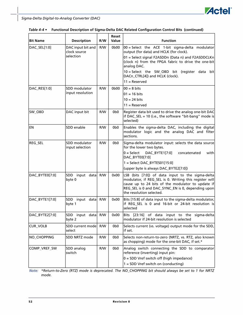
Sigma-Delta Digital-to-Analog Converter (DAC)
DAC_SEL[1:0] DAC input bit and clock source selection
R/W 0b00 00 = Select the ACE 1-bit sigma-delta modulatoroutput (for data) and HCLK (for clock).
01 = Select signal F2ASDDn (Data n) and F2ASDDCLKn(clock n) from the FPGA fabric to drive the one-bitanalog DAC.
10 = Select the SW_OBD bit (register data bitDACn_CTRL[4]) and HCLK (clock).
11 = Reserved
DAC_RES[1:0] SDD modulator input resolution
R/W 0b00 00 = 8 bits
01 = 16 bits
10 = 24 bits
11 = Reserved
SW_OBD DAC input bit R/W 0b0 Register data bit used to drive the analog one-bit DACif DAC_SEL = 10 (i.e., the software "bit-bang" mode isselected)
EN SDD enable R/W 0b0 Enables the sigma-delta DAC, including the digitalmodulator logic and the analog DAC and filtersections.
REG_SEL SDD modulator input selection
R/W 0b0 Sigma-delta modulator input: selects the data sourcefor the lower two bytes.
0 = Select DAC_BYTE1[7:0] concatenated withDAC_BYTE0[7:0]
1 = Select DAC_BYTES01[15:0]
(upper byte is always DAC_BYTE2[7:0])
DAC_BYTE0[7:0] SDD input databyte 0
R/W 0x00 LSB (bits [7:0]) of data input to the sigma-deltamodulator, if REG_SEL is 0. Writing this register willcause up to 24 bits of the modulator to update ifREG_SEL is 0 and DAC_SYNC_EN is 0, depending uponthe resolution selected.
DAC_BYTE1[7:0] SDD input databyte 1
R/W 0x00 Bits [15:8] of data input to the sigma-delta modulator,if REG_SEL is 0 and 16-bit or 24-bit resolution isselected
DAC_BYTE2[7:0] SDD input databyte 2
R/W 0x00 Bits [23:16] of data input to the sigma-deltamodulator if 24-bit resolution is selected
CUR_VOLB SDD current modeselect
R/W 0b0 Selects current (vs. voltage) output mode for the SDD,if set.
NO_CHOPPING SDD NRTZ mode R/W 0b0 Selects non-return-to-zero (NRTZ, vs. RTZ, also knownas chopping) mode for the one-bit DAC, if set.*
COMP_VREF_SW SDD analog switch
R/W 0b0 Analog switch connecting the SDD to comparatorreference (inverting) input pin:
0 = SDD Vref switch off (high impedance)
1 = SDD Vref switch on (conducting)
Table 4-4 • Functional Description of Sigma-Delta DAC Related Configuration Control Bits (continued)
Bit Name Description R/WReset Value Function
Note: *Return-to-Zero (RTZ) mode is deprecated. The NO_CHOPPING bit should always be set to 1 for NRTZmode.
52 Revision 0

SmartFusion Programmable Analog User’s Guide
Related InformationSmartFusion Intelligent Mixed-Signal FPGAs datasheet
http://www.actel.com/documents/SmartFusion_DS.pdf
DAC_MUXSEL[1:0] SDD analog multiplexer
R/W 0b00 Analog multiplexer in SCB selecting which SDD drivesthe comparator reference input pin:
00 = Select SDD0_OUT
01 = Select SDD1_OUT
10 = Select SDD2_OUT *
11 = Reserved
DAC_BYTE01[15:0] SDD input databyte 0 and byte 1
R/W 0x0000 Bits [15:0] of the data input to the sigma-deltamodulator, if REG_SEL is 1. Writing this register willcause up to 24 bits of the modulator to update ifREG_SEL is 1 and DAC_SYNC_EN is 0, depending uponthe resolution selected.
Table 4-4 • Functional Description of Sigma-Delta DAC Related Configuration Control Bits (continued)
Bit Name Description R/WReset Value Function
Note: *Return-to-Zero (RTZ) mode is deprecated. The NO_CHOPPING bit should always be set to 1 for NRTZmode.
Revision 0 53


5 – Active Bipolar Prescaler (ABPS)
ABPS Features• Selectable bipolar input ranges
• High-voltage input ranges
• High input impedance
• Factory trimmed and calibrated
• Low offset voltage
• Good gain accuracy
• Wide bandwidth/fast settling time
• Low noise
• Low operating power
• Even lower power sleep mode
• Output drives ADC input multiplexer
ABPS General DescriptionSmartFusion™ devices contain a number of active bipolar voltage-to-voltage prescalers (ABPS).There are two identical prescalers in each SmartFusion signal conditioning block (SCB). A2F200devices have four SCBs, for a total of eight prescalers in each device. The A2F500 has five SCBs, for atotal of ten prescalers in each device. The output of each prescaler goes to the analog multiplexerof one of the analog-to-digital converters (ADCs), which can select it for sampling and conversion.
The prescalers are constructed from continuous time op-amps in an inverting configuration. Thisallows the prescalers to have a large input voltage range and relatively high input impedance. Eachprescaler has an individual dynamically configurable enable that can be used to save power in casea particular prescaler is currently not being used. The gain of each prescaler is dynamicallyconfigurable, resulting in the following four nominal full-scale input ranges: ±2.56 V, ±5.12 V,±10.24 V, and ±15.36 V. Note that the maximum operating input voltage is less than ±15 V forreliability considerations, so the full implied input range of the ±15.36 V setting cannot be used.Also note that for the range selected the entire peak to peak voltage is seen by the ADC. If yoursignal only occupies 1/2 of the peak to peak input signal range, you end up using only 1/2 of theavailable ADC dynamic range.
The prescalers are coarsely trimmed for gain and offset during factory test, so their output range isjust slightly less than the 0 V to Varef (nominal 2.56 V) input range of the ADC, to guarantee theinput range limits are within range of the ADC. By default, the post processing engine (PPE) in theanalog compute engine (ACE) is used to digitally compensate most remaining gain and offseterrors using values determined during Actel’s factory test and stored in eNVM (flash memory) ineach device. In this step the gain is digitally re-inverted to account for the analog inversion in theanalog op-amp stage. Even if you choose not to use the stored factory calibration values, thedefault operation is for the PPE to apply a gain of –1 to re-invert the signal, though the default PPEmicrocode can always be overwritten.
Revision 0 55

Active Bipolar Prescaler (ABPS)
ABPS Symbol
ABPS Detailed DescriptionThe active bipolar prescaler (ABPS) senses the voltage on an input pad and scales it to fit the rangeof the ADC (nominally 0 V to 2.56 V, if the internal voltage reference, Varef, is used). It is designedusing a conventional operational amplifier with input and feedback resistances arranged in aninverting configuration. A configurable current source provides a DC offset, so the input range ofthe prescaler is shifted to be centered about ground (Figure 5-1). The feedback resistance and thecurrent source are dynamically configurable to provide one of four nominal gain and offset ranges:±2.56 V, ±5.12 V, ±10.24 V, or ±15.36 V. The feedback resistance and the level-shift current areadjusted simultaneously to implement the four ranges with the correct offset current so that theinput voltage range is always centered about zero volts.
During room-temperature factory test, Actel selects values for the gain trim, implemented as asmall discrete change in the nominal 1M ohm input resistance; and the offset trim, implemented asa small discrete change in the nominal zero volts applied to the non-inverting pin of the op-amp.
Figure 5-1 • Active Bipolar Prescaler (ABPS) Symbol
-K VOUT(to ADC Input MUX)
ABPS[n]_IN
Configuration: Enable, Range Select
Table 5-1 • Functional Block Diagram of Active Bipolar Prescaler
+
–
ABPS[[0-7]Pad
ABPS[[0-7]_IN 1 Mohm
Rin
OffsetTrim
GainTrim I Level Shift
Range Set
ABPS[0-7]
ADC 0_CH[1,2,5,6]ADC 1_CH[1,2,5,6]
Vout = –Vin*Rf/Rin + VAREF/2
VoutTo ADC
±
56 Revision 0

SmartFusion Programmable Analog User’s Guide
Table 5-2 relates each of the eight or ten ABPS blocks with the Signal Conditioning Block (SCB) inwhich it is located:
ABPS ConfigurationThe active bipolar prescalers (ABPS) can be dynamically configured via registers in the analogcompute engine (ACE). These registers can be controlled by the ACE itself, or any of the followingthree AHB bus masters: a Cortex-M3 program, by user logic (or soft processor) via the AHB busmaster connected to the FPGA fabric, or by the peripheral DMA bus master.
Each ABPS can individually be placed in a power save mode (disabled), and each ABPS can beconfigured for the desired gain/range selection.
The ABPS configuration options can be set statically using the SmartDesign MSS configurator. Theycan also be changed at any time dynamically using any of the three ABM bus masters listed above,or by the ACE’s sample sequencer engine (SSE) or post-processing engine (PPE).
Table 5-3 summarizes the configuration settings related to the active bipolar prescalers (ABPS).Only the ABPS-related bits are described here; bits in the same or adjacent registers that are usedfor other SCB configuration functions are not documented in this section.
Table 5-2 • Active Bipolar Prescaler Input Pad Designations
ADC
Signal Conditioning
BlockABPS Name Pad Name
Function Name
Shared Functions
on Pad
ADC Channel Used for ABPS
Output
ADC0 SCB0 ABPS0 ABPS0 ABPS0_IN None ADC0_CH1
ABPS1 ABPS1 ABPS1_IN ADC0_CH2
SCB1 ABPS2 ABPS2 ABPS2_IN ADC0_CH5
ABPS3 ABPS3 ABPS3_IN ADC0_CH6
ADC1 SCB2 ABPS4 ABPS4 ABPS4_IN ADC1_CH1
ABPS5 ABPS5 ABPS5_IN ADC1_CH2
SCB3 ABPS6 ABPS6 ABPS6_IN ADC1_CH5
ABPS7 ABPS7 ABPS7_IN ADC1_CH6
ADC2* SCB4* ABPS8* ABPS8 ABPS8_IN ADC2_CH1
ABPS9* ABPS9 ABPS9_IN ADC2_CH2
Note: Components indicated are available only in the A2F500.
Table 5-3 • Relative and Absolute Addresses for ABPS-Related Configuration Control Bits
SCB Byte and Bit Address (relative to each SCB)
Advanced Bus Matrix (ABM) Address
(absolute 32-bit address)1
Analog Compute Engine SSE and PPE Address
(absolute 8-bit address) Bit Name Description
SCB_0 (0x40020204/0x81 – 0x40020230/0x8C)
B8 [0] 0x40020224 [0] 0x89 [0] ABPS_EN ABPS0 enable
B8 [2:1] 0x40020224 [2:1] 0x89 [2:1] GDEC [1:0] ABPS0 range select
B8 [4] 0x40020224 [4] 0x89 [4] ABPS_EN ABPS1 enable
B8 [6:5] 0x40020224 [6:5] 0x89 [6:5] GDEC [1:0] ABPS1 range select
Notes:
1. Only the least-significant byte of each 32-bit data word is utilized.
2. Components indicated by an asterisk (*) are available only in the A2F500.
Revision 0 57

Active Bipolar Prescaler (ABPS)
Table 5-4 describes comparator-related configuration control bits.
Related InformationSmartFusion Intelligent Mixed-Signal FPGAs datasheet
http://www.actel.com/documents/SmartFusion_DS.pdf
SCB_1 (0x40020234/0x8D – 0x40020260/0x98)
B8 [0] 0x40020254 [0] 0x95 [0] ABPS_EN ABPS2 enable
B8 [2:1] 0x40020254 [2:1] 0x95 [2:1] GDEC [1:0] ABPS2 range select
B8 [4] 0x40020254 [4] 0x95 [4] ABPS_EN ABPS3 enable
B8 [6:5] 0x40020254 [6:5] 0x95 [6:5] GDEC [1:0] ABPS3 range select
SCB_2 (0x40020264/0x99 – 0x40020290/0xA4)
B8 [0] 0x40020284 [0] 0xA1 [0] ABPS_EN ABPS4 enable
B8 [2:1] 0x40020284 [2:1] 0xA1 [2:1] GDEC [1:0] ABPS4 range select
B8 [4] 0x40020284 [4] 0xA1 [4] ABPS_EN ABPS5 enable
B8 [6:5] 0x40020284 [6:5] 0xA1 [6:5] GDEC [1:0] ABPS5 range select
SCB_3 (0x40020294/0xA5 – 0x400202C0/0xB0)
B8 [0] 0x400202B4 [0] 0xAD [0] ABPS_EN ABPS6 enable
B8 [2:1] 0x400202B4 [2:1] 0xAD [2:1] GDEC [1:0] ABPS6 range select
B8 [4] 0x400202B4 [4] 0xAD [4] ABPS_EN ABPS7 enable
B8 [6:5] 0x400202B4 [6:5] 0xAD [6:5] GDEC [1:0] ABPS7 range select
SCB_4* (0x400202C4/0xB1 – 0x400202F0/0xBC)
B8 [0]C* 0x400202E4 [0]* 0xB9 [0]* ABPS_EN ABPS8 enable*
B8 [2:1]* 0x400202E4 [2:1]* 0xB9 [2:1]* GDEC [1:0] ABPS8 range select*
B8 [4]* 0x400202E4 [4]* 0xB9 [4]* ABPS_EN ABPS9 enable*
B8 [6:5]* 0x400202E4 [6:5]* 0xB9 [6:5]* GDEC [1:0] ABPS9 range select*
Table 5-3 • Relative and Absolute Addresses for ABPS-Related Configuration Control Bits (continued)
Notes:
1. Only the least-significant byte of each 32-bit data word is utilized.
2. Components indicated by an asterisk (*) are available only in the A2F500.
Table 5-4 • Functional Description of Comparator-Related Configuration Control Bits
Bit Name Description R/WReset Value Function
ABPS_EN ABPS enable R/W 0b0 0 = Power save mode; 1 = Operational mode
GDEC [1:0] ABPS range select R/W 0b00 00 = ± 15.36 V range (nominal gain = –0.08333 V/V)
01 = ± 10.24 V range (nominal gain = –0.125 V/V)
10 = ± 5.12 V range (nominal gain = –0.25 V/V)
11 = ± 2.56 V range (nominal gain = –0.5 V/V)
58 Revision 0

6 – Current Monitor
Current Monitor Features• High differential gain
• Tolerance to high common mode voltages
• Common mode voltage rejection
• Factory calibrated
• High input impedance
• Low offset voltage
• Good gain accuracy and linearity
• Low noise
• Low operating power
• Even lower power sleep mode
• Supports simultaneous sampling
• Output drives ADC
Current Monitor General DescriptionActel SmartFusion™ devices contain a number of current monitors. There is one current monitor ineach SmartFusion signal conditioning block (SCB). A2F200 devices have four SCBs, for a total of fourcurrent monitors in each device. A2F500 devices have five SCBs, for a total of five current monitorsin each device. The output of each current monitor goes to the analog multiplexer of one of theanalog-to-digital converters (ADCs), which can select it for conversion.
The current monitor amplifies a small differential voltage across its two input pins, while rejectingthe common mode voltage. The primary use intended for the current monitor is to measure thevoltage drop across a small external sense resistor placed in the path of a current. A smalldifferential voltage proportional to the current is developed across the resistor in accordance withOhm’s Law (V = I × R). For example, the current monitor and sense resistor may be used to measurethe current a power supply is providing to its load, or the current through a motor winding. It canalso be used as a general purpose differential pre-amplifier for inputs to the ADC.
Current Monitor SymbolFigure 6-1 shows the current monitor symbol.
Figure 6-1 • Current Monitor (CM) Symbol
50VOUT(to ADC Input Mux)
CM[n]_H
CM[n]_L
+
–
Configuration: Enable, Strobe, Bypass, etc.
Revision 0 59

Current Monitor
Current Monitor Detailed DescriptionThe current monitors are constructed from switched-capacitor circuits. This allows the currentmonitors to have a high common mode input voltage range, a large common mode voltagerejection ratio, and a relatively high input impedance.
The current monitor High input signal (CM[n]_H) is attached to the CM[n] pad, and the currentmonitor Low input signal (CM[n]_L) is attached to the TM[n] pad (Figure 6-2). The current monitorsenses only positive differential voltages. That is, the CM[n]_H signal voltage must be greater thanthe CM[n]_L signal voltage. Also, the common mode voltage is required to be always positive.
Because the current monitor is designed to sense only the differential voltage on its two input pins,and effectively reject the common mode voltage, the sense resistor can be placed on either side ofthe load—the ground side of the load, where the common mode voltage is low, or the high side,where the common mode voltage is high—with good results in measuring the differential voltagein either case. Placing the sense resistor on the grounded side of the load has the undesirable effectof raising the ground voltage the load sees; and also of increasing the ground resistance, whichmight affect the noise or stability of the load circuits. So it is often preferable to place the senseresistor on the high side of the load instead. The current monitor has been designed to tolerate arelatively large common mode voltage of 14.4 V. This means that the sense resistor can be placedon the high side of the load when monitoring the current of a nominal 12 V power supply,allowing for a 20% power supply tolerance.
In either placement, on the high side or low side, the voltage seen by the load will be reducedslightly due to the voltage drop across the sense resistor. The current monitor is designed to workwith the small full-scale differential voltage of just 51.2 mV, to minimize this effect. In most casesthis small voltage drop will have a negligible effect on the overall system performance, especially ifthere is a closed loop system to compensate for it; for example, a power supply having a voltagesense feedback control loop.
The current monitor has a nominal differential gain of 50 V/V, so a zero-to-51.2 mV input is scaledup to drive the SmartFusion analog-to-digital converter (ADC) to which it is connected with theoptimal full-scale signal of zero-to-2.56 V. The high gain of the current monitor allows smallersense resistors to be used. Besides resulting in a lower voltage drop, the power dissipated in thesense resistor is much less than if a higher resistance value was required, according to the square-law relationship shown in EQ 6-1:
Power (Watts) = Current (Amps)2 × Resistance (Ohms)
EQ 6-1
Each current monitor has an individual dynamically configurable enable that can be used to savepower in case that particular current monitor is currently not being used.
By default, factory calibration values are used to digitally compensate gain and offset errors usingthe post processing engine (PPE) in the analog compute engine (ACE).
60 Revision 0

SmartFusion Programmable Analog User’s Guide
Figure 6-2 shows a simplified schematic of the current monitor.
If you are using the Actel Libero® Integrated Design Environment (IDE) SmartDesign flowSmartDesign MSS configurator, many of the details of the current monitor operation will betransparent to you. SmartDesign MSS configurator automatically generates sample sequencerengine instructions for the analog compute engine to control the current monitor and ADC strobesthat are required to use the current monitor. These are suitable for most situations.
Table 6-1 on page 62 shows the sequencing of the switches in the current monitor. This sequencingis fully automated by the current monitor logic, and once started cannot be controlled except byaborting the cycle. The sequence is initiated (advanced from the idle state to the other states) byapplying one of the current monitor strobes. Removing the strobe returns the current monitor tothe idle state.
1. In the first phase, the current monitor is standing by, or idling. In this phase most of theoffset of the circuit is sensed and removed, acting as an auto-zero circuit. The circuit iseffectively armed and ready for a measurement.
2. In the second phase, the common mode input, as present on the low side input pad (TM[n]),is stored on the two large input capacitors.
3. The third is a short phase needed just to ensure proper sequencing of the switches so thepads are not shorted (break-before-make).
In the fourth and final phase, the input voltage on the large input capacitor on the op-amp’s non-inverting input is switched from the low side pad (TM[n]), to which it was connected in phase 2, tothe high side pad (CM[n]) voltage. This change in voltage, equal to the differential input voltage,forces a current to flow through the input capacitor, which in turn creates a 50-times-larger voltagechange on the smaller series capacitor.
Note: See also Table 6-4 on page 64.Figure 6-2 • Functional Block Diagram of Current Monitor
+
–
50·C
C
50·C
C S1
S2
S3
CM[n] _H
CM[n]
CM[n] _L
VOUTto ADC MUX
CM[n]
TM[n]
To TemperatureMonitor or ADCMUX and Comparator
To Comparator
S4
Bypass MUXM1CMB_MUX_SEL
ADC 0, 1, or 2Ch. 3 or Ch. 7,depending upon whichSCB the current monitoris part of.
Isolation SwitchS5
CMB_DI_ON
Revision 0 61
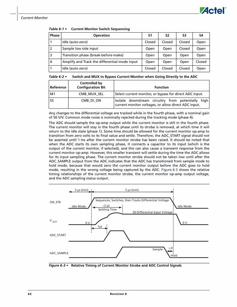
Current Monitor
Any changes to the differential voltage are tracked while in the fourth phase, with a nominal gainof 50 V/V. Common mode noise is nominally rejected during the tracking mode (phase 4).
The ADC should sample the op-amp output while the current monitor is still in the fourth phase.The current monitor will stay in the fourth phase until its strobe is removed, at which time it willreturn to the idle state (phase 1). Some time should be allowed for the current monitor op-amp totransition from zero volts to its final value and settle. Therefore, the ADC_START signal should notbe asserted until 1 ms after the current monitor strobe has been raised. It should be noted thatwhen the ADC starts its own sampling phase, it connects a capacitor to its input (which is theoutput of the current monitor, if selected), and this can also cause a transient response from thecurrent monitor op-amp. However, this smaller transient will settle during the time the ADC allowsfor its input sampling phase. The current monitor strobe should not be taken low until after theADC_SAMPLE output from the ADC indicates that the ADC has transitioned from sample mode tohold mode, because that would zero the current monitor output before the ADC goes to holdmode, resulting in the wrong voltage being captured by the ADC. Figure 6-3 shows the relativetiming relationships of the current monitor strobe, the current monitor op-amp output voltage,and the ADC sampling status output.
Table 6-1 • Current Monitor Switch Sequencing
Phase Operation S1 S2 S3 S4
1 Idle (auto-zero) Closed Closed Closed Open
2 Sample low side input Open Open Closed Open
3 Transition phase (break-before-make) Open Open Open Open
4 Amplify and Track the differential-mode input Open Open Open Closed
1 Idle (auto-zero) Closed Closed Closed Open
Table 6-2 • Switch and MUX to Bypass Current Monitor when Going Directly to the ADC
ReferenceControlled by
Configuration Bit Function
M1 CMB_MUX_SEL Select current monitor, or bypass for direct ADC input.
S5 CMB_DI_ON Isolate downstream circuitry from potentially highcurrent monitor voltages, or allow direct ADC input.
Figure 6-3 • Relative Timing of Current Monitor Strobe and ADC Control Signals
50·Differential Input Voltage
1µs
5 µs (min) 5 µs (min)
~2 µsCM_STB
Sequences, Switches, then Tracks Differential Voltage
V OUT
ADC_START
ADC_SAMPLESample
Hold
0 V
Idle ModeIdle Mode
0 V
Settling Time
> 0
62 Revision 0

SmartFusion Programmable Analog User’s Guide
Table 6-3 lists the timing requirements for current monitor strobe operations.
To facilitate simultaneous sampling of multiple current monitors, all the current monitor strobesare duplicated in one ACE register. These are referred to as the global current monitor strobes.Being collected into one register allows several current monitor strobes to be set at the sameinstant. Their function is exactly the same as the regular current monitor strobes. The global andregular strobes for each current monitor are logically ORed together. Therefore, it is important thatboth are returned to the low state after finished with their use. Starting with both the regular andglobal strobe low (the current monitor is in the idle state), then setting either the global or regularstrobe high will start the automated current monitor switch sequence, ending with the currentmonitor in track mode (phase 4) until such time as the strobe is driven low once again, forcing thecurrent monitor back to idle mode (phase 1).
It is common (though not required) to use some sort of digital filtering or averaging with thecurrent monitor in order to improve the accuracy and resolution of the result by reducing theeffect of random noise. The current monitor noise is relatively white, so the noise is reduced byroughly a factor of for an N-point equally-weighted average. Note that the ACE postprocessing engine has a built-in first-order infinite impulse response (IIR) filter that can be used. Itweights inputs exponentially, with the most recent samples receiving the highest weight. The noiseis reduced by roughly the square root of the filter passband bandwidth.
The current monitor input pads are shared with other functions. Both current monitor input padscan be used as direct ADC inputs. When used this way, the signal on the CM[n] input pin (thepositive input to the current monitor) displaces the output of the current monitor into the ADCmultiplexer. In other words, the CM[n] pin can be the input to the ADC, or the output of thecurrent monitor op-amp can be the input to the ADC, but not both at the same time since theyshare the same ADC multiplexer channel. Note that direct ADC inputs have a much lower voltagerange and voltage tolerance than the current monitors when the bypass option is selected, so caremust be taken to restrict the input voltage accordingly. When using the current monitor, there is anisolation switch which must be open to protect the downstream circuitry from the potentially highvoltages used with it.
The signal on the TM[n] input pad can also be used as a direct ADC input. Similarly to the CM[n]bypass, if used in this way the TM[n] direct input signal displaces the temperature monitor outputat the input of the ADC multiplexer.
The TM[n] input pad can also be used as the input/output pad for the temperature monitor. Whenused with the temperature monitor, the current monitor cannot be used, though the CM[n] pincould still be used as a direct ADC input. The temperature monitor is designed to withstand thesame input voltages as the current monitor, but it operates over a much smaller voltage rangewhen used for temperature sensing. This pad also has a high-voltage isolation switch which is openwhen using the current monitor but closed when using the TM[n] pad as a direct input to the ADC.For more information on the temperature monitor, see the "Temperature Monitor" section onpage 69.
Finally, there is also a comparator that shares the two input pads with the current monitor. Thecomparator positive (non-inverting) input is on the CM[n] pad, and the negative (inverting) input ison the TM[n] pad. The comparator is designed to withstand the same input voltages as the currentmonitor (up to 14.4 V) when it is disabled, but a slightly smaller voltage range (up to 9 V) whenenabled, and it is only functional over an even narrower operating voltage range (up to 2.56 V).For more about the comparators, see the "High-Speed Comparators" section on page 79.
To understand how to set the ADC input multiplexer to a selected channel, or how to configureand operate the ADC itself, see the "Analog-to-Digital Converter (ADC)" section on page 13.
Table 6-3 • Timing Requirements for Current Monitor Strobe Operation
Parameter Minimum Maximum
CM_STB(LOW) 5 µs
CM_STB(HIGH) 5 µs 200 µs
Time between Strobe start and ADC_START 1 µs
Time after ADC_SAMPLE(LOW) before CM_STB(LOW) 0 µS
N
Revision 0 63

Current Monitor
Table 6-4 relates each of the current monitor blocks with the signal conditioning block (SCB) inwhich it is located, along with the shared functions for the current monitor input pads:
Current Monitor ConfigurationThe current monitors can be dynamically configured via registers in the analog compute engine(ACE). These registers can be controlled by any of the following:
1. The ACE itself,
2. An ARM® Cortex™-M3 program
3. User logic (or soft processor) via the AHB bus master connected to the FPGA fabric
4. The peripheral DMA bus master
Each current monitor can individually be placed in a power save mode (disabled).
The strobes used to individually or collectively start and stop the current monitor automatic switchsequence are also located in ACE registers, and can be accessed in all the ways listed above.
The CM[n] and TM[n] pads used by the current monitor can be used as direct inputs to the ADC. Tofacilitate this, there is a multiplexer in the current monitor block which selects between the currentmonitor function and the direct input function for the CM[n] pad. There is also, in each case, anisolation switch which must be turned on in order to pass the direct input signal to the ADC. Whenthe current monitor is used, these two switches must be off (non-conducting) in order to protectthe downstream circuitry from the potentially high current monitor input voltages. Though themultiplexer and isolation switches have separate configuration control bits (for factory testpurposes), they are generally set or cleared together in normal operation.
The current monitor configuration options (the enable) can be set statically using the SmartDesignMSS configurator in Libero IDE. They can also be changed at any time dynamically using any of thethree ABM masters listed above, or by the ACE’s sample sequencer engine (SSE) or post-processorengine (PPE). Besides the static configuration options, the SmartDesign tool also automaticallycreates the SSE microcode required to control the current monitor strobes and ADC controlregisters.
Table 6-5 on page 65 summarizes the configuration settings related to the current monitors andcurrent monitor input pad shared functions. Only the current-monitor-related bits are describedhere; bits in the same or adjacent registers that are used for other SCB configuration functions arenot documented in this section. For information on how to select a particular ADC input channel orhow to operate the ADC, see the "Analog-to-Digital Converter (ADC)" section on page 13.
Table 6-4 • Current Monitor Input Pad Designations
ADC
Signal Conditioning
Block
Current Monitor Name
Pad Name
Function Name Shared Functions on Pad
ADC0 SCB0 CM0 CM0 CM0_H AD0_CH3 COMP0_P
TM0 CM0_L ADC0_CH4 CMP0_N TM0_IO
SCB1 CM1 CM1 CM1_H ADC0_CH7 CMP2_P
TM1 CM1_L ADC0_CH8 CMP2_N TM1_IO
ADC1 SCB2 CM2 CM2 CM2_H ADC1_CH3 CMP4_P
TM2 CM2_L ADC1_CH4 CMP4_N TM2_IO
SCB3 CM3 CM3 CM3_H ADC1_CH7 CMP6_P
TM3 CM3_L ADC1_CH8 CMP6_N TM3_IO
ADC2* SCB4* CM4* CM4* CM4_H* ADC4_CH3* CMP8_P*
TM4* CM4_L* ADC4_CH4* CMP8_N* TM4_IO*
Note: * Components indicated are available only in the A2F500.
64 Revision 0

SmartFusion Programmable Analog User’s Guide
Table 6-5 • Addresses for Current-Monitor-Related Configuration Control Bits
SCB Byte and Bit Address (relative to each SCB)
Advanced Bus Matrix (ABM) Address(absolute 32-bit
address)1
ACE SSE and PPE Address
(absolute 8-bit address) Bit Name Description
SCB_0 (0x40020204/0x81 – 0x40020230/0x8C)
B7 [0] 0x40020220 [0] 0x88 [0] CM_STB_G[0] Global CM0 strobe
B7 [1] 0x40020220 [1] 0x88 [1] CM_STB_G[1] Global CM1 strobe
B7 [2] 0x40020220 [2] 0x88 [2] CM_STB_G[2] Global CM2 strobe
B7 [3] 0x40020220 [3] 0x88 [3] CM_STB_G[3] Global CM3 strobe
B7 [4]* 0x40020220 [4] * 0x88 [4]* CM_STB_G* Global CM4 strobe*
B9 [0] 0x40020228 [0] 0x8A [0] CMB_MUX_SEL CM0 bypass MUX
B9 [1] 0x40020228 [1] 0x8A [1] CMB_DI_ON CM0 Isolation switch
B9 [2] 0x40020228 [2] 0x8A [2] CM_EN CM0 enable
B9 [3] 0x40020228 [3] 0x8A [3] CM_STB CM0 strobe
B9 [4] 0x40020228 [4] 0x8A [4] COMP_EN CMP0 comparator enable
B10 [0] 0x4002022C [0] 0x8B [0] TMB_MUX_SEL TM0 bypass MUX
B10 [1] 0x4002022C [1] 0x8B [1] TMB_DI_ON TM0 isolation switch
SCB_1 (0x40020234/0x8D – 0x40020260/0x98)
B9 [0] 0x40020258 [0] 0x96 [0] CMB_MUX_SEL CM1 bypass MUX
B9 [1] 0x40020258 [1] 0x96 [1] CMB_DI_ON CM1 isolation switch
B9 [2] 0x40020258 [2] 0x96 [2] CM_EN CM1 enable
B9 [3] 0x40020258 [3] 0x96 [3] CM_STB CM1 strobe
B9 [4] 0x40020258 [4] 0x96 [4] COMP_EN CMP2 comparator enable
B10 [0] 0x4002025C [0] 0x97 [0] TMB_MUX_SEL TM1 bypass MUX
B10 [1] 0x4002025C [1] 0x97 [1] TMB_DI_ON TM1 isolation switch
SCB_2 (0x40020264/0x99 – 0x40020290/0xA4)
B9 0x40020288 [0] 0xA2 [0] [0]CMB_MUX_SEL CM2 bypass MUX
B9 [1] 0x40020288 [1] 0xA2 [1] CMB_DI_ON CM2 isolation switch
B9 [2] 0x40020288 [2] 0xA2 [2] CM_EN CM2 enable
B9 [3] 0x40020288 [3] 0xA2 [3] CM_STB CM2 strobe
B9 [4] 0x40020288 [4] 0xA2 [4] COMP_EN CMP4 comparator enable
B10 [0] 0x4002028C [0] 0xA3 [0] TMB_MUX_SEL TM2 bypass MUX
B10 [1] 0x4002028C [1] 0xA3 [1] TMB_DI_ON TM2 isolation switch
Notes:
1. Only the least-significant byte of each 32-bit data word is utilized.
2. Components indicated with an asterisk (*) are available only in the A2F500.
Revision 0 65

Current Monitor
SCB_3 (0x40020294/0xA5 – 0x400202C0/0xB0)
B9 [0] 0x400202B8 [0] 0xAE [0] CMB_MUX_SEL CM3 bypass MUX
B9 [1] 0x400202B8 [1] 0xAE [1] CMB_DI_ON CM3 isolation switch
B9 [2] 0x400202B8 [2] 0xAE [2] CM_EN CM3 enable
B9 [3] 0x400202B8 [3] 0xAE [3] CM_STB CM3 strobe
B9 [4] 0x400202B8 [4] 0xAE [4] COMP_EN CMP6 comparator enable
B10 [0] 0x400202BC [0] 0xAF [0] TMB_MUX_SEL TM3 bypass MUX
B10 [1] 0x400202BC [1] 0xAF [1] TMB_DI_ON TM3 isolation switch
SCB_4* (0x400202C4/0xB1 – 0x400202F0/0xBC)
B9 [0]* 0x400202E8 [0]* 0xBA [0]* CMB_MUX_SEL* CM4 bypass MUX*
B9 [1]* 0x400202E8 [1]* 0xBA [1]* CMB_DI_ON* CM4 isolation switch*
B9 [2]* 0x400202E8 [2] * 0xBA [2]* CM_EN* CM4 enable*
B9 [3]* 0x400202E8 [3] * 0xBA [3]* CM_STB* CM4 strobe*
B9 [4]* 0x400202E8 [4* 0xBA [4]* COMP_EN* CMP8 comparator enable*
B10 [0]* 0x400202EC [0]* 0xBB [0]* TMB_MUX_SEL* TM4 bypass MUX*
B10 [1]* 0x400202EC [1]* 0xBB [1]* TMB_DI_ON* TM4 isolation switch*
Table 6-5 • Addresses for Current-Monitor-Related Configuration Control Bits (continued)
Notes:
1. Only the least-significant byte of each 32-bit data word is utilized.
2. Components indicated with an asterisk (*) are available only in the A2F500.
66 Revision 0

SmartFusion Programmable Analog User’s Guide
Table 6-6 gives functional descriptions for comparator-related configuration control bits.
In general, when using the current monitor, the other shared functions of the pads are not used. Ifthe current monitor is used with high input voltages, care must be taken to turn off thecomparator and isolate the ADC inputs. Therefore, the most common configuration when usingthe current monitor function is as shown in Table 6-7.
Related Information
DatasheetsSmartFusion Intelligent Mixed-Signal FPGAs datasheet
http://www.actel.com/documents/SmartFusion_DS.pdf
Table 6-6 • Functional Description of Comparator-Related Configuration Control Bits
Bit Name Description R/WReset Value Function
CMB_MUX_SEL CM bypass MUX R/W 0b0 0 = ADC input MUX driven from CM op-amp
1 = ADC input MUX driven directly from CM[n] pad
CMB_DI_ON CM isolation switch R/W 0b0 0 = Isolation switch open (isolating high voltages)
1 = Isolation switch closed (direct ADC input)
CM_EN CM enable R/W 0b0 0 = Current monitor power save mode
1= Current monitor operational mode
CM_STB CM strobe R/W 0b0 0 = Idle mode (if appropriate CM_STB_G) is also 0)
1 = Initiate sequence and leave in track mode
CM_STB_G Global CM strobe R/W 0b0 0 = Idle mode (if appropriate CM_STB is also 0)
1 = Initiate sequence and leave in track mode
COMP_EN CM enable R/W 0b0 0 = Comparator power save mode
1 = Comparator operational mode
TMB_MUX_SEL TM bypass MUX R/W 0b0 0 = ADC input MUX driven from temperature monitor
1 = ADC input MUX driven directly from TM[n] pad
TMB_DI_ON TM isolation switch R/W 0b0 0 = Isolation switch open (isolating high voltages)
1 = Isolation switch closed (direct ADC input)
Table 6-7 • Common Configuration for Current Monitor
Parameter Function
MB_MUX_SEL = 0 Selects current monitor over direct input option.
CMB_DI_ON = 0 Isolates the ADC from potentially high input voltages on CM[n].
CM_EN = 1 Turns on the current monitor.
CM_STB = {0, 1} Start in idle mode (0) and strobe (1) to start sequence.
CM_STB_G = 0 ORed with CM_STB. Not needed unless simultaneous operation of multiplecurrent monitors is required.
COMP_EN = 0 Turns off comparator (so it will tolerate highest voltages).
TMB_MUX_SEL = 0 Does not really matter, so long as the isolation switch is used.
TMB_DI_ON = 0 Isolates the ADC from potentially high input voltages on TM[n].
Revision 0 67


7 – Temperature Monitor
Temperature Monitor Features• Converts temperature to voltage
• Only one external component
• Low pin count
• Factory calibrated
• Good temperature accuracy
• Low noise
• Low operating power
• Even lower power sleep mode
• Output drives ADC
Temperature Monitor General DescriptionSmartFusion™ devices contain a number of temperature monitors. There is one temperaturemonitor in each SmartFusion signal conditioning block (SCB). A2F200 devices have four SCBs, for atotal of four temperature monitors in each device. A2F500 devices have five SCBs, for a total of fivetemperature monitors in each device. The output of each temperature monitor goes to the analogmultiplexer of one of the analog-to-digital converters (ADCs) input multiplexers, which can select itfor conversion.
The temperature monitor converts temperature to voltage using an external PN-junction, such as adiode-connected bipolar transistor or a PN-junction diode, as a temperature sensor. The diode hasits anode connected to the temperature monitor’s input-output (I/O) pad. The cathode is connectedto the temperature monitor ground pad. The temperature monitor ground pad is shared betweenthe temperature monitors in two adjacent SCBs.
The temperature monitor generates two small output currents which it applies to its input-outputpad sequentially when strobed. The difference in the two voltages developed across the PN-junction is amplified and then digitized by the ADC. This voltage is proportional to absolutetemperature using the well-known temperature dependence of the current-versus-voltagecharacteristic of PN-junction diodes. The post processing engine (PPE) in the analog computeengine (ACE) applies the factory-determined offset compensation value.
Revision 0 69

Temperature Monitor
Temperature Monitor SymbolFigure 7-1 shows the temperature monitor symbol.
Each SCB has one temperature monitor. Temperature monitors in every pair of SCBs share atemperature monitor ground. The temperature monitor outputs the stimulus currents on its I/Opin, and inputs the resulting voltages (with respect to ground) on the same pin.
In the A2F200 there are four temperature monitors, labeled TM0 through TM3, with input/outputpads also labeled TM0 through TM3. These pads are connected to signals/functions named TM0_IOthrough TM3_IO. There are two ground pads and associated signals named GNDTM0 and GNDTM1.The voltages on pads TM0 and TM1 are referenced to GNDTM0, and the voltages on pads TM2 andTM3 are referenced to GNDTM1.
In the A2F500 there are five temperature monitors, labeled TM0 through TM4, with input/outputpads also labeled TM0 through TM4. These pads are connected to signals/functions named TM0_IOthrough TM4_IO. There are three ground pads and associated signals named GNDTM0, GNDTM1,and GNDTM2. The voltages on pads TM0 and TM1 are referenced to GNDTM0, the voltages onpads TM2 and TM3 are referenced to GNDTM1, and the voltage on pad TM4 is referenced toGNDTM2.
Temperature Monitor Detailed DescriptionThe temperature monitors are constructed from switched-capacitor circuits. This allows thetemperature monitors to have a high sensitivity and a low offset.
The temperature monitor uses one input-output pad to output two sense currents, one after theother, and to measure the resulting voltage change. It is designed for use with a PN-junctionconnected from its I/O pad to the special low-noise ground pins. One good choice for thetemperature-sensing PN-junction is a 2N3904 bipolar transistor (such as can be obtained fromNational Semiconductor or Infineon), with the collector and base connected together to configureit as a diode.
The temperature characteristic of the current-voltage relationship of a PN-junction allows ajunction diode or diode-connected bipolar transistor to be used as a temperature sensor. Thechange in voltage across the diode or the base-to-emitter voltage of a bipolar transistor for twosense currents is approximated by EQ 7-1:
VBE1 – VBE2 = (KTK/q) × (ln (I1/I2))
EQ 7-1
where:
I1/I2 is the ratio of the two sense currents, and is designed to be 10:1 in the SmartFusiontemperature monitors.
ln is the logarithm, base e (Euler’s number, 2.71828…).
K is Boltzman’s constant, approximately 1.3807 x 10⁻²³ Joules/Kelvin.
q is the charge of an electron, approximately 1.6022 x 10⁻¹⁹ Coulombs.
Figure 7-1 • Temperature Monitor Symbol
V/TVout(to ADC input MUX)
TM[n]_IO
GNDTM[m]
I/O
GND
Configuration: Enable
70 Revision 0

SmartFusion Programmable Analog User’s Guide
TK is the temperature in Kelvin. The Kelvin scale is zero at the temperature absolute zero,and 273.15° at zero degrees Celsius. It increases by one for every one degree Celsius increasein temperature.
This equates to a delta VBE of approximately –200 µV/degree when the current is dropped by a ten-to-one ratio. Since the gain of the circuit is nominally –12.5, the voltage seen by the ADC is about2.5 mV per degree. In 12-bit mode, that is nominally 4 LSB-counts (or 1 count in 10-bit mode).
Table 7-1 gives the nominal scale factor for each mode.
Figure 7-2 shows a simplified schematic of the temperature monitor.
If you are using the SmartDesign MSS configurator, many of the details of the temperature monitoroperation will be transparent to you. Smart Design automatically generates sample sequencerengine microcode to control the temperature monitor and ADC strobes that are required to usethe temperature monitor that is suitable for most situations. However, it is possible to writecustomized microcode.
Table 7-2 shows the sequencing of the switches in the temperature monitor.
Table 7-1 • Nominal Scale Factor for ADC Resolution Selected
ADC Resolution Selected Nominal Scale Factor
8-bit mode 4.0 Kbit
10-bit mode 1.0 Kbit
12-bit mode 0.25 Kbit
Note: *See Table 7-4 on page 75.Figure 7-2 • Functional Block Diagram of Temperature Monitor
Table 7-2 • Temperature Monitor Switch Sequencing
Phase Operation S1 S2 S3 S4
1 Idle (auto-zero) Closed Closed Open Closed
2 Disconnect unity feedback Open Closed Open Closed
3 Disconnect auto-zero ground Open Open Open Closed
+
–
12.5·C
C
S2
S1
S4
GNDTM[m]Vout
(to ADC MUX)
TM[n]
To Current Monitor
and Comparator
M1 – Bypass MUXTMB_MUX_SEL
ADC 0, 1, or 2;Ch. 4 or Ch. 8,depending upon whichSCB the temperaturemonitor is part of.*
S5 – Isolation SwitchTMB_DI_ON
S3
TM[n]_IO
I(~10 µA)
9·I
TM[n]
Revision 0 71

Temperature Monitor
This sequencing is fully automated by the temperature monitor logic, and once started cannot becontrolled except by aborting the cycle. The sequence is initiated (advanced from the idle state tothe other states) by applying the temperature monitor strobes, as described in the steps below.Removing the strobe returns the temperature monitor to the idle state.
1. In the first phase, the temperature monitor is standing by, or idling. In this phase the offsetof the op-amp is sensed, acting as an auto-zero circuit. The circuit is effectively armed andready for a measurement. The offset of the op-amp is stored on the small capacitor. Thevoltage at the input-output pad is stored on the large capacitor (less the op-amp offset).
2. In the second short transition phase, the unity feedback of the op-amp is removed byopening switch S1. The temperature monitor automatically sequences from phase 1 to 5when the input strobe is applied.
3. The third phase is another short transition phase to disconnect the auto-zero capacitor (C)from ground so it is floating, by opening switch S2.
4. In the fourth phase the auto-zero capacitor is connected in the feedback of the op-amp. Theop-amp output should go to zero volts. The effect of the op-amp offset is cancelled. Theinput voltage due to the current being driven through the external PN-junction diode is alsoblocked. The op-amp is now configured with an inverting gain of 12.5, due to the ratio ofthe feedback and input capacitors.
5. In the fifth and final phase, the current being driven through the external diode is droppedby a ratio of 10:1. This causes a corresponding temperature-related drop in the inputvoltage, which is inverted and amplified by the op-amp. The temperature monitor remainsin this state until the strobe is removed.
6. After the op-amp output is digitized, the input strobe can be removed, putting thetemperature monitor back in its idle state.
The ADC should sample the op-amp output while the temperature monitor is still in the fifthphase. The temperature monitor will stay in the fifth phase until its strobe is removed, at whichtime it will return to the idle state (phase 1). Some time should be allowed for the temperaturemonitor op-amp to transition from zero volts to its final value and settle. Therefore, theADC_START signal should not be asserted until 5 µs after the temperature monitor strobe has beenraised. Note that when the ADC starts its own sampling phase, it connects a capacitor to its input(which is the output of the temperature monitor, if selected), and this can also cause a transientresponse from the temperature monitor op-amp. However, this smaller transient will settle duringthe time the ADC allows for its input sampling phase. The temperature monitor strobe should notbe taken low until after the ADC_SAMPLE output from the ADC indicates that the ADC has gonefrom sample mode to hold mode. Otherwise the temperature monitor output would go to zerobefore the ADC goes to hold mode, resulting in the wrong voltage being captured by the ADC.Figure 7-3 and Table 7-3 on page 74 show the relative timing relationships of the temperature
4 Connect auto-zero capacitor infeedback
Open Open Closed Closed
5 Reduce driven current 10:1,inverting and amplifying thechange in input voltage
Open Open Closed Open
1 Idle (auto-zero) Closed Closed Open Closed
Table 7-2 • Temperature Monitor Switch Sequencing
72 Revision 0

SmartFusion Programmable Analog User’s Guide
monitor strobe, the temperature monitor op-amp output voltage, and the ADC sampling statusoutput.
Figure 7-3 • Relative Timing of Temperature Monitor Strobe and ADC Control Signals
-12.5 times input voltage change
>5µs
~5µs
TM_STB
Automatically sequences temperature monitor switchesand holds resulting voltage
Vout
ADC_START
ADC_SAMPLE
Sample
Hold
Idle modeIdle mode
Settling time
>0
Revision 0 73

Temperature Monitor
It is common to use some sort of digital filtering or averaging with the temperature monitor inorder to improve the accuracy and resolution of the result by reducing the effect of random noise.The temperature monitor noise is relatively white, so the noise is reduced by roughly a factor of
for an N-point equally-weighted average. For example, if 64 samples are averaged, the randomnoise will be reduced by roughly a factor of 8. So, if the RMS noise for individual samples was 2degrees, the noise for the results after averaging might be around 1/4 degree RMS.
The ACE post processing engine has a built-in first order infinite impulse response (IIR) filter thatcan be used. It weights inputs exponentially, with the most recent samples receiving the highestweight. The noise is reduced by roughly the square-root of the filter passband bandwidth. Eachtemperature monitor has an individual dynamically configurable enable that can be used to savepower in case that particular temperature monitor is currently not being used.
By default, factory calibration values are used to digitally compensate offset errors using the postprocessing engine (PPE) in the analog compute engine (ACE). The offset of each temperaturemonitor is calibrated near room temperature at the Actel factory using an external 2N3904transistor from National Semiconductor or Infineon as the temperature sensor, and the valuestored in nonvolatile memory (eNVM) in the device. Since the measurements are only made at onetemperature, there is no temperature slope correction; however, the factory offset correction willnominally zero the combined gain and offset errors at room temperature (rather than at absolutezero).
The temperature monitor input pads are shared with other functions. The temperature monitorinput-output pad can be used as a direct ADC input. When used this way, the signal on the TM[n]input-output pad displaces the output of the temperature monitor into the ADC multiplexer. Inother words, the TM[n] pin can be the input to the ADC, or the output of the temperature monitorcan be the input to the ADC, but not both at the same time since they share the same ADCmultiplexer channel.
The TM[n] input pad can also be used as the low (inverting) pad for the current monitor. Whenused with the current monitor, the temperature monitor cannot be used. The temperature monitoris designed to withstand the same input voltages as the current monitor, but it operates over amuch smaller voltage range when used for temperature sensing. For more information on thecurrent monitor, see the "Current Monitor" section on page 59.
Note that direct ADC inputs have a much lower voltage range and voltage tolerance than thecurrent monitor and temperature monitor, so care must be taken to restrict the input voltage tothe TM[n] pad when the direct ADC bypass is selected and the isolation switch is conducting.
Finally, there is also a comparator that shares the one input pad with the temperature monitor. Thecomparator negative (inverting) input is on the TM[n] pad. The comparator is designed towithstand the same input voltages as the current monitor (up to 14.4 V) when it is disabled, but aslightly smaller voltage range (up to 9 V) when enabled. It is functional over an even narroweroperating voltage range (up to 2.56 V). For more about the comparators, see the "High-SpeedComparators" section on page 79.
To understand how to set the ADC input multiplexer to a selected channel, or how to configureand operate the ADC itself, see the "Analog-to-Digital Converter (ADC)" section on page 13.
Table 7-3 • Timing Requirements for Temperature Monitor Strobe Operation
Parameter Minimum Maximum
TM_STB (High) 10 µS 105 µS
TM_STB (Low) 5 µs
Time between strobe start and ADC_START 5 µS
Time after ADC_SAMPLE (Low) before CM_STB (Low) 0 µs
N
74 Revision 0

SmartFusion Programmable Analog User’s Guide
Table 7-4 relates each of the temperature monitor blocks to the signal conditioning block (SCB) inwhich it is located, along with the shared functions for the temperature monitor input pad.
Temperature Monitor ConfigurationThe temperature monitors can be dynamically configured via registers in the analog computeengine (ACE). These registers can be controlled by any of the following:
1. The ACE itself
2. An ARM® Cortex™-M3 program
3. User logic (or soft processor) via the AHB bus master connected to the FPGA fabric
4. The peripheral DMA bus master
Each temperature monitor can individually be placed in a power save mode (disabled). The strobesused to individually or collectively start and stop the temperature monitor automatic switchsequence are also located in ACE registers, and can be accessed in all the ways listed above.
The temperature monitor configuration options (the enable, for example) can be set staticallyusing the SmartDesign MSS configurator. They can also be changed at any time dynamically usingany of the three ABM bus masters listed above, or by the ACE’s sample sequencer engine (SSE) orpost-processor engine (PPE). Besides the static configuration options, the SmartDesign tool alsoautomatically creates the SSE microcode required to control the temperature monitor strobes andADC control registers.
Table 7-5 on page 76 summarizes the configuration settings related to the temperature monitorsand temperature monitor input pad shared functions. Only the temperature monitor related bitsare described here; bits in the same or adjacent registers that are used for other SCB configurationfunctions are not documented in this section. For information on how to select a particular ADCinput channel or how to operate the ADC, refer to the "Analog-to-Digital Converter (ADC)" sectionon page 13.
Table 7-4 • Temperature Monitor Input Pad Designations
ADC SCB
Temp. Monitor Name Pad Name
Function Name Shared Functions on Pad
ADC0 SCB0 TM0 TM0 TM0_IO ADC0_CH4 CMP0_N CM0_L
GNDTM0 TM0_GND
TM1_GND
SCB1 TM1
TM1 TM1_IO ADC0_CH8 CMP2_N CM1_L
ADC1 SCB2 TM2 TM2 TM2_IO ADC1_CH4 CMP4_N CM2_L
GNDTM1 TM2_GND
TM3_GND
SCB3 TM3
TM3 TM3_IO ADC1_CH8 CMP6_N CM3_L
ADC2* SCB4* TM4* TM4* TM4_IO* ADC2_CH4* CMP8_N* CM4_L*
GNDTM2* TM4_GND*
Note: *Components indicated are available only in the A2F500.
Revision 0 75

Temperature Monitor
Table 7-5 and Table 7-6 on page 77 summarize configuration settings related to the temperaturemonitor.
Table 7-5 • Addresses for Temperature Monitor-Related Configuration Control Bits
SCB Byte and Bit Address (relative to each SCB)
Advanced Bus Matrix (ABM) Address
(absolute 32-bit address)1
Analog Compute Engine SSE and PPE Address
(absolute 8-bit address) Bit Name Description
SCB_0 (0x40020204/0x81 – 0x40020230/0x8C)
B9 [2] 0x40020228 [2] 0x40020228 [2] CM_EN CM0 enable
B9 [4] 0x40020228 [4] 0x8A [4] COMP_EN CMP0 comparator enable
B10 [0] 0x4002022C [0] 0x8B [0] TMB_MUX_SEL TM0 bypass MUX
B10 [1] 0x4002022C [1] 0x8B [1] TMB_DI_ON TM0 isolation switch
B10 [2] 0x4002022C [2] 0x8B [2] TM_EN TM0 enable
B10 [3] 0x4002022C [3] 0x8B [3] TM_STB TM0 strobe
SCB_1 (0x40020234/0x8D – 0x40020260/0x98)
B9 [2] 0x40020258 [2] 0x96 [2] CM_EN CM1 enable
B9 [4] 0x40020258 [4] 0x96 [4] COMP_EN CMP2 comparator enable
B10 [0] 0x4002025C [0] 0x97 [0] TMB_MUX_SEL TM1 bypass MUX
B10 [1] 0x4002025C [1] 0x97 [1] TMB_DI_ON TM1 isolation switch
B10 [2] 0x4002025C [2] 0x97 [2] TM_EN TM1 enable
B10 [3] 0x4002025C [3] 0x97 [3] TM_STB TM1 strobe
SCB_2 (0x40020264/0x99 – 0x40020290/0xA4)
B9 [2] 0x40020288 [2] 0xA2 [2] CM_EN CM2 enable
B9 [4] 0x40020288 [4] 0xA2 [4] COMP_EN CMP4 comparator enable
B10 [0] 0x4002028C [0] 0xA3 [0] TMB_DI_ON TM2 bypass MUX
B10 [1] 0x4002028C [1] 0xA3 [1] TMB_DI_ON TM2 isolation switch
B10 [2] 0x4002028C [2] 0xA3 [2] TM_EN TM2 enable
B10 [3] 0x4002028C [3] 0xA3 [3] TM_STB TM2 strobe
SCB_3 (0x40020294/0xA5 – 0x400202C0/0xB0)
B9 [2] 0x400202B8 [2] 0xAE [2] CM_EN CM3 enable
B9 [4] 0x400202B8 [4] 0xAE [4] COMP_EN CMP6 comparator enable
B10 [0] 0x400202BC [0] 0xAF [0] TMB_DI_ON TM3 bypass MUX
B10 [1] 0x400202BC [1] 0xAF [1] TMB_DI_ON TM3 isolation switch
B10 [2] 0x400202BC [2] 0x97 [2] TM_EN TM3 enable
B10 [3] 0x400202BC [3] 0x97 [3] TM_STB TM3 strobe
Notes:
1. Only the least-significant byte of each 32-bit data word is utilized.
2. Components indicated with an asterisk (*) are available only in the A2F500.
76 Revision 0

SmartFusion Programmable Analog User’s Guide
When using the temperature monitor, a common configuration would be the one shown inTable 7-7:
SCB_4* (0x400202C4/0xB1 – 0x400202F0/0xBC)
B9 [2] 0x400202E8 [2] * 0xBA [2] * CM_EN* CM4 enable*
B9 [4] * 0x400202E8 [4] * 0xBA [4] * COMP_EN* CMP8 comparator enable*
B10 [0] * 0x400202EC [0] * 0xBB [0] * TMB_DI_ON* TM4 bypass MUX *
B10 [1] * 0x400202EC [1] * 0xBB [1] * TMB_DI_ON* TM4 isolation switch*
B10 [2] * 0x400202EC [2] * 0xBB [2] * TM_EN* TM4 enable*
B10 [3] * 0x400202EC [3] * 0xBB [3] * TM_STB* TM4 strobe*
Table 7-6 • Functional Description of Comparator-Related Configuration Control Bits
Bit Name Description R/WReset Value Function
TM_EN TM enable R/W 0b0 0 = Power save mode
1 = Operational mode
TM_STB TM strobe R/W 0b0 0 = Idle mode
1 = Initiate sequence and enter hold mode
CM_EN CM enable R/W 0b0 0 = Current monitor power save mode
1 = Current monitor operational mode
COMP_EN CMP enable R/W 0b0 0 = Comparator power save mode
1 = Comparator operational mode
TMB_MUX_SEL TM bypass MUX R/W 0b0 0 = ADC input MUX driven from temperature monitor
1 = ADC input MUX driven directly from TM[n] pad
TMB_DI_ON TM isolation switch R/W 0b0 0 = Isolation switch open (isolating high voltages)
1 = Isolation switch closed (direct ADC input)
Table 7-5 • Addresses for Temperature Monitor-Related Configuration Control Bits (continued)
SCB Byte and Bit Address (relative to each SCB)
Advanced Bus Matrix (ABM) Address
(absolute 32-bit address)1
Analog Compute Engine SSE and PPE Address
(absolute 8-bit address) Bit Name Description
Notes:
1. Only the least-significant byte of each 32-bit data word is utilized.
2. Components indicated with an asterisk (*) are available only in the A2F500.
Table 7-7 • Common Configuration for Temperature Monitor
Parameter Function
TM_EN = 1 Temperature monitor operational mode
TM_STB = {0, 1} Start in idle mode (0) and strobe (1) to start sequence.
CM_EN = 0 Disable current monitor.
COMP_EN = 0 Disable comparator.
TMB_MUX = 0 Selects temperature monitor over direct input option.
TMB_DI_ON = 0 High-voltage isolation switch open
Revision 0 77

Related InformationSmartFusion Intelligent Mixed-Signal FPGAs Datasheet
http://www.actel.com/documents/SmartFusion_DS.pdf

8 – High-Speed Comparators
Comparator Features• Fast response time
• Continuous-time operation
• Differential inputs
• Programmable hysteresis
• Large common mode input range
• Large over-voltage tolerance
• DAC can supply threshold voltage
• Low input bias and offset currents
• Low offset voltage
• Low operating power
• Even lower power sleep mode
• Output drives FPGA fabric directly
• Output can be read by ARM® Cortex™-M3
• Cortex-M3 edge-triggered interrupts
Comparator General DescriptionSmartFusion™ devices contain a number of differential, analog input, high speed, continuous-timecomparators with programmable hysteresis. There are two identical comparators in eachSmartFusion signal conditioning block (SCB), though their input pads are connected to differentshared circuits. A2F200 devices have four SCBs, for a total of eight comparators in each device.A2F500 devices have five SCBs, for a total of ten comparators in each device. The digital output ofeach comparator goes to the FPGA fabric, where it can be used as an input to the configurablelogic. Output also goes to the analog compute engine (ACE) where it can be read or used togenerate edge-triggered interrupts to the Cortex-M3.
SymbolFigure 8-1 shows the Comparator symbol.
Figure 8-1 • Comparator Symbol
CMP[n](to FPGA fabric and to ACE)
–
+CMP[n]_P
CMP[n]_N
Configuration: Hysteresis, Power Save
CMP[n]
Revision 0 79

High-Speed Comparators
Comparator Detailed DescriptionThe comparator generates a digital output signal based upon the instantaneous voltage differencemeasured at its two input pins. If the positive input, CMP[n]_P, voltage is greater than the negative,or inverting input, CMP[n]_N, (also sometimes called the reference input in DC applications), theoutput, CMP[n], is a logic 1. The character [n] is replaced by the comparator instance number, 0through 7 in the A2F200 or 0 through 9 in the A2F500. If the negative input has the more positivevoltage, the comparator output is a logic zero. The comparators are designed to respond almostexclusively to the differential input voltage, and to be insensitive to the common mode voltage onthe inputs. The design of the comparator also minimizes the effect of power supply variations andtemperature on performance.
One comparator in each SCB (designated CMP0, CMP2, CMP4, CMP6, or CMP8; with an eveninstance number) gets its two inputs from pins which it shares with the current monitor andtemperature monitor. The other comparator (designated CMP1, CMP3, CMP5, CMP7, or CMP9; withan odd instance number) gets its two inputs from pins shared with SmartFusion direct ADC andLVTTL inputs. See Figure 8-2. Since the comparators share their input pins with these otherfunctions, it may not be feasible in many cases to use a comparator if the alternate pin function isbeing used. The comparators are designed to tolerate the large common mode or differential over-voltages that may be normal for the alternate function, such as the current monitor, which isdesigned to measure the current on power supplies of +12 V or more if the comparator is disabled.If enabled, the comparator voltage tolerance is reduced somewhat, and in any case the comparatoronly functions with input voltages up to 2.56 V.
For a detailed description of the current monitor function, which shares pads CM[n] and TM[n]with a comparator, see the "Current Monitor" section on page 59.
Note: *Components are available only in the A2F500.Figure 8-2 • Connections for the Two Comparators in SmartFusion SCBs
CM[0, 1, 2, 3, 4*]
+
–
CMP[0, 2, 4, 6, 8*]
+
–
CMP[1, 3, 5, 7, 9*]
To ADC Input MUX(direct inputs)
To Current andTemperatureMonitors
From Sigma–Delta DACs
(reserved)
Optional Board–Level Sample–and–Hold or FilterCapacitor
To FPGA Fabricand to ACE
To FPGA Fabricand to ACE
Bits from Dynamic Configuration Registers:(HYS[1:0], COMP_EN, 2 places)
Optional Voltage Reference
DACMUX_SEL[1:0]
COMP_VREF_SW
TM[0, 1, 2, 3, 4*]
ADC[0, 2, 4, 6, 8*]
ADC[1, 3, 5, 7, 9*]
SDD Multiplexer
SDDM[0, 1, 2, 3, 4*]
CMP[0, 2, 4, 6, 8*]_P
CMP[0, 2, 4, 6, 8*]_N
CMP[0, 2, 4, 6, 8*]
CMP[1, 3, 5, 7, 9*]
CMP[1,3,5,7,9†]_P
CMP[1,3,5,7,9†]_N
CH
*
Bits from DynamicConfiguration Registers
80 Revision 0

SmartFusion Programmable Analog User’s Guide
For a detailed description of the temperature monitor function, which shares the pad TM[n] with acomparator, see the "Temperature Monitor" section on page 69.
To understand how to set the ADC input multiplexer to a selected channel, or how to configureand operate the ADC itself, see the "Analog-to-Digital Converter (ADC)" section on page 13.
Table 8-1 relates each of the current monitor blocks to the signal conditioning block (SCB) in whichit is located along with the shared functions for the current monitor input pads:
The negative input terminal of the second (odd-numbered) comparator can be fed a referencesignal selected by an analog multiplexer from any of the SmartFusion on-chip sigma-delta DACs(SDDs). The selected DAC output signal is connected to the comparator and ADC direct input pinvia an analog switch that can be controlled by the ACE. Thus, any of the SmartFusion SDDs can beused to provide the reference (inverting) input to the odd-numbered comparator in each signalconditioning block. By placing a sample-and-hold capacitor on this pin at the board level (shown asCH in Figure 8-2 on page 80), it is possible to timeshare the SDD output. The sample-and-holdcapacitor must be recharged periodically when the voltage level stored on the capacitor droopsdue to current leakage. Since the hold (droop) time can be designed to be longer than the sampletime, one SDD can service multiple sample-and-hold capacitors, being de-multiplexed using theanalog switch in each SCB.
Alternatively, the SDD can be dedicated to continuously supply a reference voltage to one orpossibly more of the odd-numbered comparators in different SCBs in parallel, in which case a
Table 8-1 • Comparator Input Pad Designations and Shared Functions
ADC/ SDD
Signal Conditioning
BlockComparator
Name Pad NameFunction
Name Shared Functions on Pad
ADC0
SDD0
SCB0 CMP0 CM0 CMP0_P ADC0_CH3 CM0_H
TM0 CMP0_N ADC0_CH4 CM0_L TM0_IO
CMP1 ADC0 CMP1_P ADC0_CH9 LVTTL0_IN
ADC1 CMP1_N ADC0_CH10 LVTTL1_IN SDDM0_OUT
SCB1 CMP2 CM1 CMP2_P ADC0_CH7 CM1_H
TM1 CMP2_N ADC0_CH8 CM1_L TM1_IO
CMP3 ADC2 CMP3_P ADC0_CH11 LVTTL2_IN
ADC3 CMP3_N ADC0_CH12 LVTTL3_IN SDDM1_OUT
ADC1
SDD1
SCB2 CMP4 CM2 CMP4_P ADC1_CH3 CM2_H
TM2 CMP4_N ADC1_CH4 CM2_L TM2_IO
CMP5 ADC4 CMP5_P ADC1_CH9 LVTTL4_IN
ADC5 CMP5_N ADC1_CH10 LVTTL5_IN SDDM2_OUT
SCB3 CMP6 CM3 CMP6_P ADC1_CH7 CM3_H
TM3 CMP6_N ADC1_CH8 CM3_L TM3_IO
CMP7 ADC6 CMP7_P ADC1_CH11 LVTTL6_IN
ADC7 CMP7_N ADC1_CH12 LVTTL7_IN SDDM3_OUT
ADC2*
SDD2*
SCB4* CMP8* CM4* CMP8_P* ADC2_CH3* CM4_H*
TM4* CMP8_N* ADC2_CH4* CM4_L* TM4_IO*
CMP9* ADC8* CMP9_P* ADC2_CH9* LVTTL8_IN*
ADC9* CMP9_N* ADC2_CH10* LVTTL9_IN* SDDM4_OUT*
Note: *Components indicated are only available in the A2F500.
Revision 0 81

High-Speed Comparators
board-level capacitor is optional, since the SDD includes a third-order on-chip low-pass filteralready. Using the capacitor in this case may help further reduce the noise coming from the SDD orfrom other sources by forming a fourth low-pass filter pole, potentially with a much lower cutofffrequency than the on-chip filter poles, due to the availability of much larger capacitors at theboard level.
The hysteresis of each comparator is individually configurable. There are four possible settings: nohysteresis (0 mV), ±10 mV, ±30 mV, and ±100 mV nominal hysteresis. The hysteresis acts upon thethreshold for both rising and falling signals. For example, if the hysteresis were set to ±10 mV, thecomparator would only respond to a rising signal once the voltage on the positive input terminalexceeded that on the negative terminal by approximately 10 mV. For a falling signal, thecomparator output would switch state only once the voltage on the positive input terminal was10 mV less than that on the negative terminal. Therefore, a total of 20 mV exists between thepositive-going and negative-going threshold voltages when using the ±10 mV setting. These arenominal hysteresis values which will only be approximated in an actual device. The comparatorinput offset voltage will shift both threshold voltages slightly up or down, as well.
Comparator ConfigurationThe comparator can be dynamically configured via registers in the analog compute engine (ACE).These registers can be controlled by the ACE itself, a Cortex-M3 program, by user logic (or softprocessor) via the AHB bus master connected to the FPGA fabric, or by the peripheral DMA busmaster.
The comparators can individually be placed in a power save mode (disabled), and each comparatorcan be configured for the desired hysteresis selection.
Configuration settings closely related to the comparator include the SDD analog multiplexer, whichselects the DAC that will potentially drive the comparator reference pin in each signal conditioningblock, and the analog switch, which actually connects or disconnects the selected digital-to-analogconverter to the odd-numbered comparator negative input pin. The analog switch also can be usedto provide sample-and-hold operation if a board-level sample-and-hold capacitor is connected tothe ADC[1, 3, 5, 7, 9] pad (the CMP[1, 3, 5, 7, 9]_N function): when the switch is closed, the SDDcharges the capacitor (sample mode). When the switch is open, the capacitor holds the voltage towhich it has been charged (hold mode).
The comparator and comparator-related configuration options can be set statically using theSmartDesign MSS configurator. They can also be changed at any time dynamically using any of thethree ABM bus masters listed above, or by the ACE’s sample sequencer engine (SSE) or post-processing engine (PPE).
Table 8-2 gives a comparison of relative and absolute addresses for configuration control bits.
Table 8-2 • Relative and Absolute Addresses for Comparator-Related Configuration Control Bits
SCB Byte and Bit Address(relative to each SCB)
Advanced Bus Matrix (ABM)
Address(absolute 32-bit
address)1
Analog Compute
Engine SSE and PPE Address
(absolute 8-bit address) Bit Name Description
SCB_0 (0x40020204/0x81 – 0x40020230/0x8C)
B9[4] 0x40020228 [4] 0x8A [4] COMP_EN CMP0 Enable
B9[7:6] 0x40020228 [7:6] 0x8A [7:6] HYS[1:0] CMP0 Hysteresis
B10[4] 0x4002022C [4] 0x8B [4] COMP_EN CMP1 Enable
Notes:
1. Only the least-significant byte of each 32-bit data word is utilized.
2. Components indicated with an asterisk (*) are available only in the A2F500.
82 Revision 0

SmartFusion Programmable Analog User’s Guide
B10[5] 0x4002022C [5] 0x8B [5] COMP_VREF_SW SCB0 SDD Analog Switch (toCMP1)
B10[7:6] 0x4002022C [7:6] 0x8B [7:6] HYS[1:0] CMP1 Hysteresis
B11[1:0] 0x40020230 [1:0] 0x8C [1:0] DAC_MUXSEL[1:0] SDDM0 Analog MUX (to CMP1)
SCB_1 (0x40020234/0x8D – 0x40020260/0x98)
B9[4] 0x40020258 [4] 0x96 [4] COMP_EN CMP2 Enable
B9[7:6] 0x40020258 [7:6] 0x96 [7:6] HYS[1:0] CMP2 Hysteresis
B10[4] 0x4002025C [4] 0x97 [4] COMP_EN CMP3 Enable
B10[5] 0x4002025C [5] 0x97 [5] COMP_VREF_SW SCB1 SDD Analog Switch (toCMP3)
B10[7:6] 0x4002025C [7:6] 0x97 [7:6] HYS[1:0] CMP3 Hysteresis
B11[1:0] 0x40020260 [1:0] 0x98 [1:0] DAC_MUXSEL[1:0] SDDM1 Analog MUX (to CMP3)
SCB_2 (0x40020264/0x99 – 0x40020290/0xA4)
B9[4] 0x40020288 [4] 0xA2 [4] COMP_EN CMP4 Enable
B9[7:6] 0x40020288 [7:6] 0xA2 [7:6] HYS[1:0] CMP4 Hysteresis
B10[4] 0x4002028C [4] 0xA3 [4] COMP_EN CMP5 Enable
B10[5] 0x4002028C [5] 0xA3 [5] COMP_VREF_SW SCB2 SDD Analog Switch (toCMP5)
B10[7:6] 0x4002028C [7:6] 0xA3 [7:6] HYS[1:0] CMP5 Hysteresis
B11[1:0] 0x40020290 [1:0] 0xA4 [1:0] DAC_MUXSEL[1:0] SDDM2 Analog MUX (to CMP5)
SCB_3 (0x40020294/0xA5 – 0x400202C0/0xB0)
B9[4] 0x400202B8 [4] 0xAE [4] COMP_EN CMP6 Enable
B9[7:6] 0x400202B8 [7:6] 0xAE [7:6] HYS[1:0] CMP6 Hysteresis
B10[4] 0x400202BC [4] 0xAF [4] COMP_EN CMP7 Enable
B10[5] 0x400202BC [5] 0xAF [5] COMP_VREF_SW SCB3 SDD Analog Switch (toCMP7)
B10[7:6] 0x400202BC [7:6] 0xAF [7:6] HYS[1:0] CMP7 Hysteresis
B11[1:0] 0x400202C0 [1:0] 0xB0 [1:0] DAC_MUXSEL[1:0] SDDM3 Analog MUX (to CMP7)
SCB_4* (0x400202C4/0xB1 – 0x400202F0/0xBC)
B9[4]* 0x400202E8 [4]* 0xBA [4]* COMP_EN* CMP8 Enable*
B9[7:6]* 0x400202E8 [7:6]* 0xBA [7:6]* HYS[1:0]* CMP8 Hysteresis*
B10[4]* 0x400202EC [4]* 0xBB [4]* COMP_EN* CMP9 Enable*
B10[5]* 0x400202EC [5]* 0xBB [5]* COMP_VREF_SW* SCB4 SDD Analog Switch (toCMP9)*
Table 8-2 • Relative and Absolute Addresses for Comparator-Related Configuration Control Bits (continued)
SCB Byte and Bit Address(relative to each SCB)
Advanced Bus Matrix (ABM)
Address(absolute 32-bit
address)1
Analog Compute
Engine SSE and PPE Address
(absolute 8-bit address) Bit Name Description
Notes:
1. Only the least-significant byte of each 32-bit data word is utilized.
2. Components indicated with an asterisk (*) are available only in the A2F500.
Revision 0 83

High-Speed Comparators
Table 8-3 gives the functions of the Comparator configuration control bits.
B10[7:6]* 0x400202EC [7:6]* 0xBB [7:6]* HYS[1:0]* CMP9 Hysteresis*
B11[1:0]* 0x400202F0 [1:0]* 0xBC [1:0]* DAC_MUXSEL[1:0]* SDDM4 Analog MUX (toCMP9)*
Table 8-2 • Relative and Absolute Addresses for Comparator-Related Configuration Control Bits (continued)
SCB Byte and Bit Address(relative to each SCB)
Advanced Bus Matrix (ABM)
Address(absolute 32-bit
address)1
Analog Compute
Engine SSE and PPE Address
(absolute 8-bit address) Bit Name Description
Notes:
1. Only the least-significant byte of each 32-bit data word is utilized.
2. Components indicated with an asterisk (*) are available only in the A2F500.
Table 8-3 • Functional Description of Comparator-Related Configuration Control Bits
Bit Name Description R/WReset Value Function
COMP_EN Comparator Enable
R/W 0b0 0 = Power Save (Comparator Output = TBD)
1 = Operational Mode
HYS[1:0] Comparator Hysteresis
R/W 0b00 00 = No Hysteresis
01 = ± 10 mV nominal
10 = ± 30 mV nominal
11 = ± 100 mV nominal
COMP_VREF_SW SDD Analog Switch
R/W 0b0 0 = SDD VREF switch off (high impedance)
1 = SDD VREF switch on (conducting)
DAC_MUXSEL[1:0] SDD Analog Multiplexer
R/W 0b00 00 = Select SDD0_OUT
01 = Select SDD1_OUT
10 = Select SDD2_OUT*
11 = Reserved
Note: * Components indicated are only available in the A2F500.
84 Revision 0

SmartFusion Programmable Analog User’s Guide
Comparator Outputs and InterruptsThe comparator outputs go directly to the FPGA fabric, where they can be used to driveconfigurable logic, and also to the analog compute engine (ACE), where they are mapped into thememory space of the Cortex-M3 via the advanced high-speed bus matrix (ABM). There they can beread by three ABM bus masters: the Cortex-M3, the FPGA fabric, and the peripheral DMA busmasters. In addition, the ACE can use any of the comparator outputs to generate an edge-triggeredinterrupt to the Cortex-M3.
To use the high-speed comparator outputs in user logic in the FPGA fabric, the relevantcomparators must be instantiated in the SmartDesign MSS configurator for the analog computeengine, and then the ACE output ports that appear can be stitched to other blocks in the design.Table 8-4 gives the register map for the comparator.
The COMPARATOR_STATUS register (Table 8-5) is used to read the output status of the comparatorsby any of the three bus masters with access to the ACE slave. If the comparator INP pin is morepositive than the INN pin at the time of the read command (accounting for propagation delays),then the corresponding bit in the comparator output status register will be read as a logical 1.
The registers shown in Table 8-6 on page 86 record an edge-triggered event on any of thecomparator digital output signals. Each of the eight or ten comparator outputs drives two bits: onefor detecting a rising edge, and one for detecting a falling edge. These events can be used totrigger an interrupt in the Cortex-M3 priority interrupt logic.
Table 8-4 • Comparator Register Map
Register NameABM
Address R/W Reset Value Description
COMPARATOR_STATUS 0x4002100C R 0x000 Comparator Output Levels
COMP_IRQ_EN 0x4002120C R/W 0x000000 Comparator interrupt enables
COMP_IRQ 0x40021210 R 0x000000 Comparator edges detected
COMP_IRQ_CLR 0x40021214 W 0x000000 Clears COMP_IRQ bits
Table 8-5 • Comparator Status Output Register Bit Fields
Bit Number Name R/W Reset Value Description / Location
31:10 Reserved R Reserved
9* COMPARATOR R 0b0 CMP9 Output*
8* COMPARATOR R 0b0 CMP8 Output*
7 COMPARATOR R 0b0 CMP7 Output
6 COMPARATOR R 0b0 CMP6 Output
5 COMPARATOR R 0b0 CMP5 Output
4 COMPARATOR R 0b0 CMP4 Output
3 COMPARATOR R 0b0 CMP3 Output
2 COMPARATOR R 0b0 CMP2 Output
1 COMPARATOR R 0b0 CMP1 Output
0 COMPARATOR R 0b0 CMP0 Output
Note: * Bits indicated are only available in the A2F500; otherwise they are reserved.
Revision 0 85

High-Speed Comparators
Events can be masked and cleared by other registers, as shown in Table 8-6.
COMP_IRQ_EN bits are logically ANDed with the bits in the COMP_IRQ register to create interruptsto the Cortex-M3. If any of the bits in this register are logic 1, the corresponding bit in theCOMP_IRQ register is enabled; otherwise the corresponding bit in the COMP_IRQ register isdisabled/masked in its contribution to the interrupt outputs.
Table 8-6 • Bit Mapping Between Comparators, Interrupt Control Registers, and Cortex-M3 Interrupts
COMP_IRQ_EN COMP_IRQ COMP_IRQ_CLR Register Name
0x4002120C 0x40021210 0x40021214 Register Address in ABM Address Space
R/W R W R/W
0x000000 0x000000 0x000000 Reset Value
Bit NumberCortex-M3
Interrupt No.Relevant Comparator and Edge
(Rising or Falling)
31:24 31:24 31:24 Reserved
Comparator Rising Edge Interrupts
23:22 23:22 23:22 108-107 Reserved
21* 21* 21* 106* CMP9 Output Rising*
20* 20* 20* 105* CMP8 Output Rising*
19 19 19 104 CMP7 Output Rising
18 18 18 103 CMP6 Output Rising
17 17 17 102 CMP5 Output Rising
16 16 16 101 CMP4 Output Rising
15 15 15 100 CMP3 Output Rising
14 14 14 99 CMP2 Output Rising
13 13 13 98 CMP1 Output Rising
12 12 12 97 CMP0 Output Rising
Comparator Falling Edge Interrupts
11:10 11:10 11:10 96:95 Reserved
9* 9* 9* 94* CMP9 Output Falling*
8* 8* 8* 93* CMP8 Output Falling*
7 7 7 92 CMP7 Output Falling
6 6 6 91 CMP6 Output Falling
5 5 5 90 CMP5 Output Falling
4 4 4 89 CMP4 Output Falling
3 3 3 88 CMP3 Output Falling
2 2 2 87 CMP2 Output Falling
1 1 1 86 CMP1 Output Falling
0 0 0 85 CMP0 Output Falling
Note: * Bits indicated are only available in the A2F500; otherwise they are reserved.
86 Revision 0

SmartFusion Programmable Analog User’s Guide
Set bits in the COMP_IRQ register indicate rising or falling edge events on any or all digital outputsof the eight comparators in the SmartFusion FPGA Signal Conditioning Blocks (SCBs). These bits arebitwise logically ANDed with bits in COMP_IRQ_EN to create Cortex-M3 interrupts.
The write-only bits in the COMP_IRQ_CLR register are used to clear corresponding bits in theCOMP_IRQ register. Writing a 1 to any of the bits will clear the corresponding bits in the COMP_IRQregister, while writing a 0 to any of the bits will have no effect. In the event that writing a 1 tothese clear bits coincides with a set event in the COMP_IRQ register, the set event shall have higherpriority.
Comparator Application – Using One SDD to Set Multiple Comparator Reference Voltages
Each sigma-delta digital-to-analog converter (SDD) goes to an analog multiplexer in each of thesignal conditioning blocks (SCBs). The output of the multiplexer goes to an analog switch, whichcan be used as input to a board-level hold capacitor (see Figure 8-2 on page 80.) One SDD can driveseveral of these hold capacitors—up to one per SCB—by setting the multiplexer in each SCB toselect the same SDD. Then, by controlling the analog switches, the selected DAC can alternately beconnected to each of the several hold capacitors while simultaneously changing the digital value atthe input of the SDD in a time-division fashion. The analog switches act together to de-multiplexthe piecewise analog signal, with one piece (potentially unique voltage) being applied to each ofthe hold capacitors.
The approximate time-constant and cutoff (–3 dB) frequency of the new pole generated by addinga board-level capacitor (CH) can be calculated using the nominal output impedance of the sigma-delta DAC, which is RDAC = 10 KΩ:
τc = RDAC × CH seconds
EQ 8-1
fc = 1 / (2π RDAC × CH) Hz
EQ 8-2
For example, the time-constant and cutoff frequency formed by setting CH = 100 nF are 1 ms and159 Hz, respectively.
To achieve settling to a 0.1 percent accuracy (2.56 mV) requires approximately 7 time-constants(note 10-3 ≅ e-6.9), or for this example, about 7 milliseconds. This would be the sample timerequired for the SDD to impose a large change of voltage on CH.
Bias and leakage currents will cause the hold capacitor to droop while it is in hold mode. The drooprate is proportional to the bias current and inversely proportional to the size of the hold capacitor.For example, if CH = 100 nF and the bias current is IB = 0.5 μA (maximum), the droop rate is5 µV / µs, maximum. The shortest time in which a one percent error could develop would be 5.1 ms.
The DC bias current creates a DC offset voltage. This is computed as the bias current times the DACoutput impedance. If the bias current is IB = 0.5 µA and the DAC output resistance is RDAC = 10 KΩ,then the offset voltage generated would be VOFFSET = 5 mV.
Revision 0 87

High-Speed Comparators
When refreshing a nominally constant voltage there will be some ripple due to the droop that iscaused by bias currents during the hold mode, followed by the exponential charging in the samplemode (in combination with the continuing bias currents). In the steady state, these two voltagesare equal in amplitude (Figure 8-3.
The length of the sample is time T and the total time to cycle through N capacitors is then N timesT, with N being 2, 3, or 4, since the A2F200 has four SCBs. Each capacitor is refreshed for a time, T,and then droops for a time, (N-1) × T, while the remaining capacitors are serviced.
EQ 8-3 shows VRIPPLE computed two ways; one based upon the droop during the hold period, andthe other based upon the exponential charging that occurs during the sample period less thedroop during that phase:
EQ 8-3
where e is Euler’s number (2.71828...)
Solving for VPK gives EQ 8-4.
EQ 8-4
For example, if:
IB = 0.5 µA (maximum bias current)
CH = 100 nF (hold capacitor capacitance)
RDAC = 10 KΩ (SDD typical output impedance)
T = 100 µs (sample time)
N = 4 (total number of sample periods)
Then:
VOFFSET = 5 mV (maximum DC offset due to bias current)
VRIPPLE = 1.5 mV (peak-to-peak AC ripple due to droop and refresh cycle)
VPK = 2.21 mV (maximum excursion due to refresh cycle; not including VOFFSET)
Figure 8-3 • Steady-State Waveform with Ripple Due to Drooping and Recharging
Time
V
VIDEAL = Target Voltage
Offset Voltage Caused by Bias Current
VOFFSET
VPK = Max. Excursion(not incl. VOFFSET)
TSample Time
(charge)
(N–1)·THold Time(droop)
VRIPPLE
VRIPPLE
IBCH------- N 1–( ) T⋅ ⋅ e
TRDAC CH⋅------------------------⎝ ⎠⎛ ⎞–
VPK
IBCH------- T⋅⎝ ⎠⎛ ⎞–⋅= =
VPK
IB N T eT
CH RDAC⋅------------------------⎝ ⎠⎛ ⎞
⋅ ⋅ ⋅
CH-----------------------------------------------------------=
88 Revision 0

SmartFusion Programmable Analog User’s Guide
τC = 1 ms (exponential charging time-constant)
fC = 159 Hz (–3 dB cutoff frequency)
VRIPPLE and VPK can be reduced by selecting a larger hold capacitor, in which case the chargingtime-constant will also increase (so the time required for a large change in voltage will be longer)and the cutoff frequency will decrease. VRIPPLE and VPK can also be reduced by decreasing thesample time, though if it gets too short then secondary effects such as charge injection from theanalog switch could start to become a factor.
Related Information
DatasheetsSmartFusion Intelligent Mixed-Signal FPGAs Datasheet
http://www.actel.com/documents/SmartFusion_DS.pdf
User’s GuidesSmartFusion Microcontroller Subsystem User’s Guide
http://www.actel.com/documents/SmartFusion_MSS_UG.pdf
Revision 0 89


9 – Direct ADC Inputs
Direct ADC Input Features• Input drives ADC input MUX directly
• No active amplifiers in signal chain
• Full ADC accuracy
• Wide bandwidth
• Each channel factory calibrated
• Low noise
• No additional power required
Direct ADC Input General DescriptionSmartFusion™ devices contain a number of direct ADC input paths. These signal paths go directlyto the ADC main multiplexer without going through any active gain stages; they go only throughsome analog switches. If that channel is selected by the ADC multiplexer, the input pad iseffectively connected directly to the sampling capacitor of the ADC. The operational input voltagerange of direct inputs is from zero to VAREF (nominally 2.56 V, unless VAREF is externally supplied).
The direct ADC inputs are arrayed as follows:
• For each signal conditioning block (SCB) there are two direct ADC inputs, both sharing theirinput pads with the current monitor (and other functions).
• There are four additional direct ADC Inputs associated with every ADC, almost all of whichshare their input pads with comparators.
• There is one direct ADC input associated with each DAC, sharing its input pad with the DACoutput.
In the A2F200 there are four SCBs, which have eight possible direct ADC inputs, plus there are twoADCs with another eight direct ADC inputs, and two DACs, each with a direct ADC input, for a totalof up to 18 direct ADC inputs.
In the A2F500 there are five SCBs having ten possible direct ADC inputs, plus there are three ADCshaving another twelve direct ADC inputs, and three DACs, each with a direct ADC input, for a totalof up to 25 direct ADC inputs. Because the third ADC in the A2F500 has only one SCB associatedwith it instead of two, two of the direct ADC inputs associated with the ADC do not have acomparator connected in parallel, as all the others do.
The post Processing Engine (PPE) in the Analog Compute Engine (ACE) applies the factory-determined offset and gain compensation values for each Direct ADC Input channel.
Direct ADC Input Symbol
In the signal/function name shown, the ADC number “[n]” can be one of [0, 1] for the A2F200 and[0, 1, 2] for the A2F300. The channel number “m” can be one of [3, 4, 7, 8, 9, 10, 11, 12, 15].
Figure 9-1 • Direct ADC Input Symbol
VOUT(to ADC Input MUX)
ADC[n]_CH[m]
Revision 0 91

Direct ADC Inputs
Channels [3, 4, 7, 8] are those that are associated with current and temperature monitors. (Thosemonitors can be bypassed for a Direct ADC Input path). Channels [9, 10, 11, 12] are those whichshare inputs with comparators, and channel 15 shares its input with the SDD output. This is shownmore explicitly in Figure 6 below.
Direct ADC Input Detailed DescriptionThere are three main types of direct ADC inputs:
1. Those that share pads with the current monitor (in addition to other functions) which havepotentially high input voltages at their input pads
2. Those that share pads with comparators only
3. Those that share pads with the Sigma-Delta DAC output
The inputs that are shared with the current monitor have additional multiplexing in the signal pathin order to select the direct inputs, bypassing the current monitor and/or temperature monitoroutputs with which they share ADC input channels. They also have isolation switches to protect theADC and the ADC main input multiplexer from the potentially high voltages that could be presenton these pads when the current monitor is in use.
The inputs that are shared only with the comparators, which operate at voltages compatible withthe ADC, go directly to the ADC main input multiplexer, as do the inputs that are shared with theDAC outputs.
Because the only circuit elements in the signal path are relatively low impedance analog switches,the performance of the Direct ADC Inputs is dominated by the ADC itself. Because there is nointentional filtering and there are no active gain stages in these paths, they have the highestbandwidth of any SmartFusion ADC inputs. Signals very close to the Nyquist frequency may besampled by the ADC via these input channels.
Figure 9-1and Figure 9-2 show simplified schematics of the Direct ADC Inputs:
Table 9-1 • Direct ADC Inputs Sharing Inputs with the Current and Temperature Monitors (direct paths highlighted)
Isolation SwitchCMB_DI_ON
ADC[0,1,2†]_CH[3,7]
ADC[0,1,2†]_CH[4,8]
TM[0,1,2,3,4†]
CM[0,1,2,3,4†]
CM[0,1,2,3,4†]
TM[0,1,2,3,4†]
CMP[0,2,4,6,8†]_N
CMP[0,2,4,6,8†]_P CMP[0,2,4,6,8†]
To Comparator
TM[n]_IO
CM[n]_L
+
-
CM[n]_H
Isolation SwitchCMB_DI_ON
Bypass MUXCMB_MUX_SEL
Bypass MUXCMB_MUX_SEL
50
V/T
92 Revision 0

SmartFusion Programmable Analog User’s Guide
If you are using the Libero Smart Design flow, many of the details of the Direct ADC Inputs will betransparent to you. When you select a Direct ADC Input, Smart Design automatically configures thevarious isolation and bypass switches, and creates the Sample Sequencer Engine microcode tocontrol the ADC strobes that are required to use the Direct ADC Inputs that is suitable for mostsituations. However, it is possible to write customized microcode.
By default, factory calibration values are used to digitally compensate offset and gain errors usingthe Post Processing Engine (PPE) in the Analog Compute Engine (ACE).
The Direct ADC Inputs pads are shared with other functions. The temperature monitor input-output pad (TM[n]) can be used in conjunction with an external temperature sensing diode tosense temperature. When used as a Direct ADC Input, the signal on the TM[n] pad displaces theoutput of the temperature monitor into the ADC multiplexer. In other words, the TM[n] pad can bethe input to the ADC, or the output of the temperature monitor can be the input to the ADC, butnot both at the same time since they share the same ADC multiplexer channel. For moreinformation on the temperature monitor, see the Temperature Monitor section of the SmartFusionIntelligent Mixed-Signal FPGAs datasheet.
The CM[n] and TM[n] input pads can alternatively be used for the current monitor. When used withthe current monitor, the current monitor output uses the ADC input channel which could havebeen used for the CM[n] pad as a Direct ADC Input. Similar to the case with the temperaturemonitor, the ADC channel can be used for either the current monitor output, or the CM[n] padDirect ADC Input, but not both.
If you are using the current monitor, it may be possible to also use the TM[n] input as a Direct ADCInput to measure the voltage on the low side of the current monitor sense resistor, but great caremust be taken to observe the maximum voltage ratings of the TM[n] inputs in this case. Also beaware that the ADC input range might not include ground due to small offset voltages. Taking intoconsideration these limitations, this technique might be useful for measuring both the current andthe voltage of a power supply that is within the Direct ADC Input range, for example a 1.5V or 1.8Vsupply, using a high-side current sense resistor and measuring the low side of the resistor using thedirect input path from the TM[n] pad.
Figure 9-2 • Direct ADC Inputs Sharing Inputs with Comparators, and with the Sigma-Delta DAC (direct paths highlighted)
}
{
}
SDD[0,1,2†]SDD[0,1,2†]_OUT
SDDM[0,2,4†]_OUT
COPM_VREF_SW COPM_VREF_SW
DAC_MUX_SEL[1:0]DAC_MUX_SEL[1:0]
from other 1 or 2 DACs
from ACE
SDDM[1,3]_OUT
ADC[0,4,8†]
ADC[1,5,9†]
ADC[2,6,10†]
ADC[3,7,11†]
ADC[0,1,2†]_CH[9]
ADC[0,1,2†]_CH[10]
ADC[0,1,2†]_CH[11]
ADC[0,1,2†]_CH[12]
CMP[1,5,9†]_P
CMP[1,5,9†]_Nto Comparator CMP[1,5,9†]and LVTTL[0,1,4,5,8†,9†]
to Comparator CMP[3,7]and LVTTL[2,3,6,7,10†,11†]
CMP[3,7]_P
CMP[3,7]_N
ADC[0,1,2†]_CH[15]
D/A
Revision 0 93

Direct ADC Inputs
Note that direct ADC inputs have a much lower voltage range and voltage tolerance than thecurrent monitor and temperature monitor, so care must be taken to restrict the input voltages tothe CM[n] and TM[n] pads when the direct ADC bypass(es) are selected and the high voltageisolation switch(es) are conducting. For more information on the current monitor, see the "CurrentMonitor" section on page 59.
Finally, there is also a comparator that shares the same two pads (TM[n] and CM[n]). Since theDirect ADC Input and the comparator have generally compatible voltage ranges, it may be feasibleto use both on the same signals. For more about the comparators, see the "High-SpeedComparators" section on page 79 and the comparator section of the SmartFusion IntelligentMixed-Signal FPGAs datasheet.
For every ADC there are four input pads designated as Direct ADC Inputs, (ADC[n]). These pads arealso shared with comparators (which use two pads each). The reference (i.e. negative) input of thecomparators can be driven by the Sigma-Delta DAC; generally this is done in a time-shared fashion,if used. See the "Direct ADC Inputs" section on page 91 where demultiplexing the DAC output togenerate reference voltages for one or more comparators is described in more detail.
These four input pads also go to LVTTL digital input buffers. So, if the pads are not needed forDirect ADC Inputs or for use with the comparators, they may be used as standard LVTTL digitalinputs. These inputs go directly to the FPGA fabric. Enables for each of the LVTTL input bufferscome directly from the FPGA fabric.
To understand how to set the ADC input multiplexer to a selected channel, or how to configureand operate the ADC itself, see the "Analog-to-Digital Converter (ADC)" section on page 13.
Table 9-2 relates each of the Direct ADC Inputs with the shared functions on the same input pads.
Table 9-2 • Direct ADC Input Pad Designations
ADC/ SDD
Signal Conditioning
BlockPad
NameFunction
Name Shared Functions on Pad
ADC0
SDD0
SCB0 CM0 ADC0_CH3 CMP0_P CM0_H
TM0 ADC0_CH4 CMP0_N CM0_L TM0_IO
ADC0 ADC0_CH9 CMP1_P LVTTL0_IN
ADC1 ADC0_CH10 CMP1_N LVTTL1_IN SDDM0_OUT
SCB1 CM1 ADC0_CH7 CMP2_P CM1_H
TM1 ADC0_CH8 CMP2_N CM1_L TM1_IO
ADC2 ADC0_CH11 CMP3_P LVTTL2_IN
ADC3 ADC0_CH12 CMP3_N LVTTL3_IN SDDM1_OUT
(N/A) SDD0 ADC0_CH15 SDD0_OUT
ADC1
SDD1
SCB2 CM2 ADC1_CH3 CMP4_P CM2_H
TM2 ADC1_CH4 CMP4_N CM2_L TM2_IO
ADC4 ADC1_CH9 CMP5_P LVTTL4_IN
ADC5 ADC1_CH10 CMP5_N LVTTL5_IN SDDM2_OUT
SCB3 CM3 ADC1_CH7 CMP6_P CM3_H
TM3 ADC1_CH8 CMP6_N CM3_L TM3_IO
ADC6 ADC1_CH11 CMP7_P LVTTL6_IN
ADC7 ADC1_CH12 CMP7_N LVTTL7_IN SDDM3_OUT
(N/A) SDD1 ADC1_CH15 SDD1_OUT
Note: *Components indicated are only available in the A2F500.
94 Revision 0

SmartFusion Programmable Analog User’s Guide
Direct ADC Input ConfigurationThe Direct ADC Inputs can be dynamically configured via registers in the Analog Compute Engine(ACE). These registers can be controlled by the ACE itself, a Cortex-M3 program, by user logic (orsoft processor) via the AHB bus master connected to the FPGA Fabric, or by the Peripheral DMA busmaster.
The Direct ADC Input configuration options can be set statically using the Libero Smart Design toolinside the provided Analog Compute Engine graphical configurator. They can also be changed atany time dynamically using any of the three advanced bus matrix (ABM) bus masters listed above,or by the ACE’s Sample Sequencer Engine (SSE) or Post-Processor Engine (PPE). Besides the staticconfiguration options, the Smart Design tool also automatically creates the SSE microcode requiredto control the ADC and the ADC’s main multiplexer control registers and strobes.
To use the Direct ADC Inputs associated with the CM[n] and TM[n] pads, the appropriate isolationswitch(es) must be conducting, and the bypass multiplexer put into the bypass mode. Special caremust be taken when the isolation switch is conducting to observe the reduced maximum ratings ofthe inputs.
To use the Direct ADC Inputs associated with pads ADC[1, 3, 5, 7, 9, or 11] the COMP_VREF_SWshould be in the off, or non-conducting state.
To use the Direct ADC Inputs associated with the SDD[n] output pads, the DAC should be in thecurrent output mode. In the voltage output mode there will be an additional 10 Khoum load toground. Also, the DAC duty factor should be zero, or else it will be driving a current out on this pin.
In most cases, it will also be desirable to put any unused alternate functions attached to the padsused for Direct ADC Inputs into their respective power-down states.
Table 9-3 on page 96 summarizes the configuration settings related to the Direct ADC Inputs andfunctions sharing the same input pads which may need controlling in order to use the direct paths.Only the Direct ADC Input related bits are described here; bits in the same or adjacent registers thatare used for other SCB configuration functions are not documented in this section. For how to
ADC2*
SDD2*
SCB4 CM4 ADC2_CH3 CMP8_P CM4_H
TM4 ADC2_CH4 CMP8_N CM4_L TM4_IO
ADC8 ADC2_CH9 CMP9_P LVTTL8_IN
ADC9 ADC2_CH10 CMP9_N LVTTL9_IN SDDM4_OUT
(N/A) SDD2 ADC2_CH15 SDD2_OUT
Table 9-2 • Direct ADC Input Pad Designations
ADC/ SDD
Signal Conditioning
BlockPad
NameFunction
Name Shared Functions on Pad
Note: *Components indicated are only available in the A2F500.
Revision 0 95

Direct ADC Inputs
select a particular ADC input channel or how to operate the ADC see the ADC section of thisdatasheet.
Table 9-3 • Relative and Absolute Addresses for Direct ADC Input Related Configuration Control Bits
SCB Byte and Bit Address (relative)
ABM Address(absolute 32-bit
address)1
ACE, SSE, and PPE Address
(absolute 8-bit Address) Bit Name Description
SCB_0 (0x40020204/0x81 through 0x40020230/0x8C)
B6[0] 0x4002021C [0] 0x87 [0] CUR_VOLB SDD0 current/voltage select
B9[0] 0x40020228 [0] 0x8A [0] CMB_MUX_SEL CM0 bypass MUX
B9[1] 0x40020228 [1] 0x8A [1] CMB_DI_ON CM0 isolation switch
B9[2] 0x40020228 [2] 0x8A [2] CM_EN CM0 enable
B9 [4] 0x40020228 [4] 0x8A [4] COMP_EN CMP0 comparator enable
B10 [0] 0x4002022C [0] 0x8B [0] TMB_MUX_SEL TM0 bypass MUX
B10 [1] 0x4002022C [1] 0x8B [1] TMB_DI_ON TM0 isolation switch
B10 [2] 0x4002022C [2] 0x8B [2] TM_EN TM0 enable
B10[4] 0x4002022C [4] 0x8B [4] COMP_EN CMP1 comparator enable
B10[5] 0x4002022C [5] 0x8B [5] COMP_VREF_SW SCB0 SDD analog switch (to ADC1)
SCB_1 (0x40020234/0x8D through 0x40020260/0x98)
B9[0] 0x40020258 [0] 0x96 [0] CMB_MUX_SEL CM1 bypass MUX
B9[1] 0x40020258 [1] 0x96 [1] CMB_DI_ON CM1 isolation switch
B9[2] 0x40020258 [2] 0x96 [2] CM_EN CM1 enable
B9 [4] 0x40020258 [4] 0x96 [4] COMP_EN CMP2 comparator enable
B10 [0] 0x4002025C [0] 0x97 [0] TMB_MUX_SEL TM1 bypass MUX
B10 [1] 0x4002025C [1] 0x97 [1] TMB_DI_ON TM1 isolation switch
B10 [2] 0x4002025C [2] 0x97 [2] TM_EN TM1 enable
B10[4] 0x4002025C [4] 0x97 [4] COMP_EN CMP3 comparator enable
B10[5] 0x4002025C [5] 0x97 [5] COMP_VREF_SW SCB1 SDD analog switch (to ADC3)
Notes:
1. Only the least-significant byte of each 32-bit data word is utilized.
2. Components indicated are only available in the A2F500.
96 Revision 0

SmartFusion Programmable Analog User’s Guide
SCB_2 (0x40020264/0x99 through 0x40020290/0xA4)
B6[0] 0x4002027C [0] 0x9F [0] CUR_VOLB SDD1 current/voltage Sel.
B9[0] 0x40020288 [0] 0x A2 [0] CMB_MUX_SEL CM2 bypass MUX
B9[1] 0x40020288 [1] 0x A2 [1] CMB_DI_ON CM2 isolation switch
B9[2] 0x40020288 [2] 0x A2 [2] CM_EN CM2 enable
B9 [4] 0x40020288 [4] 0xA2 [4] COMP_EN CMP4 comparator enable
B10 [0] 0x4002028C [0] 0xA3 [0] TMB_DI_ON TM2 bypass MUX
B10 [1] 0x4002028C [1] 0xA3 [1] TMB_DI_ON TM2 isolation switch
B10 [2] 0x4002028C [2] 0xA3 [2] TM_EN TM2 enable
B10[4] 0x4002028C [4] 0xA3 [4] COMP_EN CMP5 comparator enable
B10[5] 0x4002028C [5] 0xA3 [5] COMP_VREF_SW SCB2 SDD analog switch (to ADC5)
SCB_3 (0x40020294/0xA5 through 0x400202C0/0xB0)
B9[0] 0x400202B8 [0] 0x AE [0] CMB_MUX_SEL CM3 bypass MUX
B9[1] 0x400202B8 [1] 0x AE [1] CMB_DI_ON CM3 isolation switch
B9[2] 0x400202B8 [2] 0x AE [2] CM_EN CM3 enable
B9 [4] 0x400202B8 [4] 0xAE [4] COMP_EN CMP6 comparator enable
B10 [0] 0x400202BC [0] 0xAF [0] TMB_DI_ON TM3 bypass MUX
B10 [1] 0x400202BC [1] 0xAF [1] TMB_DI_ON TM3 isolation switch
B10 [2] 0x400202BC [2] 0xAF [2] TM_EN TM3 enable
B10[4] 0x400202BC [4] 0xAF [4] COMP_EN CMP7 comparator enable
B10[5] 0x400202BC [5] 0xAF [5] COMP_VREF_SW SCB3 SDD analog switch (to ADC7)
SCB_4 (0x400202C4/0xB1 through 0x400202F0/0xBC)2
B6[0] 0x400202DC [0] 0xB7 [0] CUR_VOLB SDD2 current/voltage select
B9[0] 0x400202E8 [0] 0x BA [0] CMB_MUX_SEL CM4 bypass MUX
B9[1] 0x400202E8 [1] 0x BA [1] CMB_DI_ON CM4 isolation switch
B9[2] 0x400202E8 [2] 0x BA [2] CM_EN CM4 enable
B9 [4] 0x400202E8 [4] 0xBA [4] COMP_EN CMP8 comparator enable
B10 [0] 0x400202EC [0] 0xBB [0] TMB_DI_O TM4 bypass MUX
B10 [1] 0x400202EC [1] 0xBB [1] TMB_DI_ON TM4 isolation switch
B10 [2] 0x400202EC [2] 0xBB [2] TM_EN TM4 enable
B10[4] 0x400202EC [4] 0xBB [4] COMP_EN CMP9 comparator enable
B10[5] 0x400202EC [5] 0xBB [5] COMP_VREF_SW SCB4 SDD analog switch (to ADC9)
Table 9-3 • Relative and Absolute Addresses for Direct ADC Input Related Configuration Control Bits
SCB Byte and Bit Address (relative)
ABM Address(absolute 32-bit
address)1
ACE, SSE, and PPE Address
(absolute 8-bit Address) Bit Name Description
Notes:
1. Only the least-significant byte of each 32-bit data word is utilized.
2. Components indicated are only available in the A2F500.
Revision 0 97

Direct ADC Inputs
Related InformationSmartFusion Intelligent Mixed-Signal FPGAs datasheet
http://www.actel.com/documents/SmartFusion_DS.pdf
Table 9-4 • Functional Description of Direct ADC Input Related Configuration Control Bits
Bit Name Description R/WReset Value Function
CUR_VOLB SDD Current Mode R/W 0b0 0 = Voltage mode
1 = Current mode
COMP_EN CMP Enable R/W 0b0 0 = Comparator Power Save mode
1 = Comparator Operational mode
CM_EN CM Enable R/W 0b0 0 = Power Save mode
1 = Operational mode
CMB_MUX_SEL CM Bypass MUX R/W 0b0 0 = ADC input MUX driven from current monitor
1 = ADC input MUX driven directly from CM[n] pad
CMB_DI_ON CM Isolation Switch R/W 0b0 0 = Isolation switch open (isolating high voltages)
1= Isolation switch closed (direct ADC input)
TM_EN TM Enable R/W 0b0 0 = Power Save mode
1 = Operational mode
TMB_MUX_SEL TM Bypass MUX R/W 0b0 0 = ADC input MUX driven from temperature monitor
1 = ADC input MUX driven directly from TM[n] pad
TMB_DI_ON TM Isolation Switch R/W 0b0 0 =Isolation switch open (isolating high voltages)
1 = Isolation switch closed (direct ADC input)
COMP_VREF_SW SDD Analog Switch R/W 0b0 0 = SDD Vref Switch off (high impedance)
1 = SDD Vref Switch on (conducting)
98 Revision 0

A – List of Changes
The following table lists critical changes that were made in the current version of the SmartFusionProgrammable Analog User’s Guide.
Previous Version Changes in Current Version (Revision 0) Page
Draft B(December 2009)
Table 2-1 • Analog Front-End Input Pad Designations and Shared Functionswas replaced.
11
The integral nonlinearity (INL) error for 10-bit mode was revised to 0.8 in the"Key Features" section.
13
Figure 3-2 • Example SAR ADC Architecture was revised to indicate there isone/2N-1 capacitor, not two.
14
The "Acquisition Time or Sample Time Control" section was revised tochange the units of sample time to microseconds (µs) rather than seconds.
21
Figure 3-11 • Intra-Conversion and Figure 3-12 • Injected Conversion wereinterchanged; they had been mislabeled in the previous version of thedocument.
25, 26
EQ 3-17 was revised to indicate that the value of CALIBRATE is 1. 28
VREFSEL was changed to VAREFSEL in Table 3-13 • ADCx_MISC_CTRL. 32
Bit 5 was changed from PWRDWN to PWRDWN_x in Table 3-9 •ANA_COMM_CTRL.
31
Figure 6-2 • Functional Block Diagram of Current Monitor was corrected bychanging SBC to SCB. CBM MUX_SEL was changed to CMB_MUX_SEL.
61
The first column heading in Table 6-5 • Addresses for Current-Monitor-Related Configuration Control Bits was changed to clarify that the addressesare relative to each SCB. The CM_STB_G entries were revised toCM_STB_G[0] through CM_STB_G[3].
65
The first column heading in Table 8-2 • Relative and Absolute Addresses forComparator-Related Configuration Control Bits was changed to clarify thatthe addresses are relative to each SCB.
82
Table 8-6 • Bit Mapping Between Comparators, Interrupt Control Registers,and Cortex-M3 Interrupts was revised to change the relative comparatorand edge from CMP7 and CMP6 output falling to CMP9 and CMP8 for bits 9and 8.
86
Draft A(September 2009)
Figure 1-1 • Analog Compute Engine (A2F500 shown) was revised to showthat ADC Unit 2 has one signal conditioning block (SCB), not two.
5
The "SmartFusion Analog Features" section was revised. 9
The "Key Features" section was revised. 13
Table 3-7 • ADC Memory Map was revised to change all register addressesfrom an address of the form 0x4001XXXX to an address of the form0x4002XXXX.
29
The "ABPS General Description" section was updated to revise theparagraph beginning with the sentence, "The prescalers are constructedfrom continuous time op-amps in an inverting configuration."
55
Revision 0 99

List of Changes
Draft A(continued)
The "ABPS Configuration" section was revised to clarify that the ACEregisters can be controlled by AHB bus masters.
57
The first column heading in Table 5-3 • Relative and Absolute Addresses forABPS-Related Configuration Control Bits was changed to clarify that theaddresses are relative to each SCB.
57
The "Current Monitor Configuration" section was revised. 64
The "Temperature Monitor Detailed Description" section was revised tosuggest a choice for a temperature-sensing PN-junction.
70
Table 7-1 • Nominal Scale Factor for ADC Resolution Selected is new. 71
The first column heading in Table 7-5 • Addresses for Temperature Monitor-Related Configuration Control Bits was changed to clarify that the addressesare relative to each SCB.
76
Previous Version Changes in Current Version (Revision 0) Page
100 Revision 0

B – Product Support
Actel backs its products with various support services including Customer Service, a CustomerTechnical Support Center, a web site, an FTP site, electronic mail, and worldwide sales offices. Thisappendix contains information about contacting Actel and using these support services.
Customer ServiceContact Customer Service for non-technical product support, such as product pricing, productupgrades, update information, order status, and authorization.
From Northeast and North Central U.S.A., call 650.318.4480From Southeast and Southwest U.S.A., call 650. 318.4480From South Central U.S.A., call 650.318.4434From Northwest U.S.A., call 650.318.4434From Canada, call 650.318.4480From Europe, call 650.318.4252 or +44 (0) 1276 401 500From Japan, call 650.318.4743From the rest of the world, call 650.318.4743Fax, from anywhere in the world 650.318.8044
Actel Customer Technical Support CenterActel staffs its Customer Technical Support Center with highly skilled engineers who can helpanswer your hardware, software, and design questions. The Customer Technical Support Centerspends a great deal of time creating application notes and answers to FAQs. So, before you contactus, please visit our online resources. It is very likely we have already answered your questions.
Actel Technical SupportVisit the Actel Customer Support website (www.actel.com/support/search/default.aspx) for moreinformation and support. Many answers available on the searchable web resource includediagrams, illustrations, and links to other resources on the Actel web site.
WebsiteYou can browse a variety of technical and non-technical information on Actel’s home page, atwww.actel.com.
Contacting the Customer Technical Support CenterHighly skilled engineers staff the Technical Support Center from 7:00 a.m. to 6:00 p.m., Pacific Time,Monday through Friday. Several ways of contacting the Center follow:
EmailYou can communicate your technical questions to our email address and receive answers back byemail, fax, or phone. Also, if you have design problems, you can email your design files to receiveassistance. We constantly monitor the email account throughout the day. When sending yourrequest to us, please be sure to include your full name, company name, and your contactinformation for efficient processing of your request.
101

Product Support
The technical support email address is [email protected].
PhoneOur Technical Support Center answers all calls. The center retrieves information, such as your name,company name, phone number and your question, and then issues a case number. The Center thenforwards the information to a queue where the first available application engineer receives thedata and returns your call. The phone hours are from 7:00 a.m. to 6:00 p.m., Pacific Time, Mondaythrough Friday. The Technical Support numbers are:
650.318.4460800.262.1060
Customers needing assistance outside the US time zones can either contact technical support viaemail ([email protected]) or contact a local sales office. Sales office listings can be found atwww.actel.com/company/contact/default.aspx.
102

Index
AABPS
block diagram 56configuration 57control bits addresses 57detailed description 56features 55general description 55input pad designations 57
ACEblock diagram 5functional description 6interrupts 7register map 48used to configure services 6
acquisition time control 21Actel
electronic mail 101telephone 102web-based technical support 101website 101
active bipolar prescaler (ABPS) 55ADC
block diagram 13calibration 26clock 23configuration example 28conversion 24example architecture 14interrupts 27key features 13power control 26register map 29resolution 24startup sequence 27terminology 16theory of operation 14
ADC_SYNC_CONV 30ADCx_CONV_CTRL 31ADCx_MISC_CTRL 32ADCx_STATUS 33ADCx_STC 32ADCx_TVC 32AFE
configuration 12functions and location in SCB 11general description 9overview 9
ANA_COMM_CTRL 31analog
block diagram 11low-pass filter 41
analog compute engine (ACE) 6analog front-end (AFE) 5analog multiplexer (MUX) 21analog-to-digital converter (ADC) 13
Ccomparator
application 87bit mapping 86configuration 82connections 80control bits addresses 82detailed description 80features 79input pad designations 81interrupts 85register map 85shared functions 81status output register bit fields 85
contacting Actelcustomer service 101electronic mail 101telephone 102web-based technical support 101
conversion example 15current monitor
common configuration 67control bits addresses 65detailed description 60features 59general description 59input pad designations 64switch sequence 62timing 62
current monitor configuration 64customer service 101
DDAC
one-bit converter 40differential non-linearity (DNL) 16direct ADC input
configuration 95control bits addresses 96detailed description 92features 91input pad designations 94sharing inputs 92, 93
DNL 16
Eeffective number of bits (ENOB) 16
103

Index
ENOB 16
FFS error 16full-scale error (FS error) 16
Ggain error 17
drift 17
IINL 18integral non-linearity (INL) 18interrupts
ACE 7ADC 27comparator 86
Lleast significant bit (LSB) 18LSB 18
Mmodulator
block diagram 39
Ooffset error 18
Pproduct support 102
customer service 101electronic mail 101technical support 101telephone 102website 101
Rregister map
ACE 48ADC 29comparator 85
resolution 19
Ssample time control 21sampling rate 19SCB
features contained in each 10SD DAC
configuration 47control bits and addresses 49description 35detailed description 38effect of external capacitor 41frequency domain 43generic block diagram 37input examples 43input/output pad designations 46interpolation and reconstruction 44low-pass filtering 45modulation 44principle 36shared pins 46SmartFusion block diagram 39time-domain 43
sigma-delta digital-to-analog converter (SD DAC) 35signal-to-noise and distortion (SINAD) 19signal-to-noise ratio (SNR) 19SINAD 19SNR 19
Ttechnical support 101temperature monitor
block diagram 71common configuration 77control bit addresses 76description 69detailed description 70features 69input pad designations 75nominal scale factor 71switch sequencing 71timing 73
timingcurrent monitor strobe operation 63temperature monitor 73
total harmonic distortion 20total unadjusted error 20TUE 20
Vvoltage reference, integrated 27
Wweb-based technical support 101
104

50200251-0/3.10
Actel Corporation
2061 Stierlin CourtMountain View, CA94043-4655 USAPhone 650.318.4200Fax 650.318.4600
Actel Europe Ltd.
River Court,Meadows Business ParkStation Approach, BlackwaterCamberley Surrey GU17 9ABUnited KingdomPhone +44 (0) 1276 609 300Fax +44 (0) 1276 607 540
Actel Japan
EXOS Ebisu Buillding 4F1-24-14 Ebisu Shibuya-kuTokyo 150 JapanPhone +81.03.3445.7671Fax +81.03.3445.7668http://jp.actel.com
Actel Hong Kong
Room 2107, China Resources Building26 Harbour RoadWanchai, Hong KongPhone +852 2185 6460Fax +852 2185 6488www.actel.com.cn
Actel is the leader in low-power FPGAs and mixed-signal FPGAs and offers the most comprehensive portfolio of system and power management solutions. Power Matters. Learn more at www.actel.com.
© 2010 Actel Corporation. All rights reserved. Actel, Actel Fusion, IGLOO, Libero, Pigeon Point, ProASIC, SmartFusion and the associated logos aretrademarks or registered trademarks of Actel Corporation. All other trademarks and service marks are the property of their respective owners.