a transforming metal nanocomposite with large …li.mit.edu/a/papers/13/hao13cuiscience.pdf · a...
TRANSCRIPT

initially aligned with this direction emitted purecircularly polarized photons and remained in-variant under scattering. Their superpositions, onthe other hand, became entangled with the scat-tered photon polarization. States that are invariantunder coupling to the environment are of interest,not only because of their importance in the quan-tum measurement process but also because oftheir potential use for quantum control purposes.Invariant states can span decoherence-free sub-spaces in which quantum information can beprotected (21). It would be therefore interestingto search for multi-spin states that are invariantunder photon scattering, and detection, by usinglarger arrays of trapped ions.
References and Notes1. W. H. Zurek, Rev. Mod. Phys. 75, 715 (2003).2. This mechanism is different than the process of
ein-selection in decoherence theory, in which the mutualinteraction between a quantum system, a measurement
apparatus, and their environment results in theemergence of a preferred basis (1).
3. C. J. Myatt et al., Nature 403, 269 (2000).4. M. Brune et al., Phys. Rev. Lett. 77, 4887 (1996).5. M. S. Chapman et al., Phys. Rev. Lett. 75, 3783 (1995).6. M. Mei, M. Weitz, Phys. Rev. Lett. 86, 559 (2001).7. D. A. Kokorowski, A. D. Cronin, T. D. Roberts,
D. E. Pritchard, Phys. Rev. Lett. 86, 2191 (2001).8. R. Ozeri et al., Phys. Rev. Lett. 95, 030403 (2005).9. H. Uys et al., Phys. Rev. Lett. 105, 200401 (2010).10. N. Akerman, S. Kotler, Y. Glickman, R. Ozeri, Phys. Rev.
Lett. 109, 103601 (2012).11. D. B. Hume, T. Rosenband, D. J. Wineland, Phys. Rev.
Lett. 99, 120502 (2007).12. A. H. Myerson et al., Phys. Rev. Lett. 100, 200502 (2008).13. A. Keselman, Y. Glickman, N. Akerman, S. Kotler,
R. Ozeri, New J. Phys. 13, 073027 (2011).14. B. B. Blinov, D. L. Moehring, L. M. Duan, C. Monroe,
Nature 428, 153 (2004).15. J. Volz et al., Phys. Rev. Lett. 96, 030404 (2006).16. N. Akerman, S. Kotler, Y. Glickman, A. Keselman,
R. Ozeri, App. Phys. B, 10.1007/s00340-011-4807-6 (2011).
17. Materials and methods are available as supplementarymaterials on Science Online.
18. Cohen-Tannoudji, Claude and Diu, Bernard and Laloe,Frank, Quantum Mechanics (Wiley-Interscience 2006),Vol. 2, p. 1048.
19. M. A. Nielsen, I. L. Chuang, Quantum Computation andQuantum Information (Cambridge Univ. Press,Cambridge, 2000).
20. M. B. Plenio, S. Virmani, Quant. Inf. Comput. 7,1 (2007).
21. D. A. Lidar, I. L. Chuang, K. B. Whaly, Phys. Rev. Lett. 81,2594 (1998).
Acknowledgments: Y.G. and S.K. have equally contributedto this work. We thank N. Davidsson and D. Stamper-Kurnfor useful comments on the manuscript. We gratefullyacknowledge the support by the Israeli Science Foundation,the Minerva Foundation, the German-Israeli Foundationfor scientific research, the Crown Photonics Center, andM. Kushner Schnur, Mexico.
Supplementary Materialswww.sciencemag.org/cgi/content/full/339/6124/1187/DC1Materials and MethodsFigs. S1 to S4
3 September 2012; accepted 2 January 201310.1126/science.1229650
A Transforming Metal Nanocompositewith Large Elastic Strain, LowModulus, and High StrengthShijie Hao,1 Lishan Cui,1* Daqiang Jiang,1 Xiaodong Han,2* Yang Ren,3* Jiang Jiang,1
Yinong Liu,4 Zhenyang Liu,1 Shengcheng Mao,2 Yandong Wang,5 Yan Li,6 Xiaobing Ren,7,8
Xiangdong Ding,7 Shan Wang,1 Cun Yu,1 Xiaobin Shi,1 Minshu Du,1 Feng Yang,1
Yanjun Zheng,1 Ze Zhang,2,9 Xiaodong Li,10 Dennis E. Brown,11 Ju Li7,12*
Freestanding nanowires have ultrahigh elastic strain limits (4 to 7%) and yield strengths,but exploiting their intrinsic mechanical properties in bulk composites has proven to be difficult.We exploited the intrinsic mechanical properties of nanowires in a phase-transforming matrixbased on the concept of elastic and transformation strain matching. By engineering the microstructureand residual stress to couple the true elasticity of Nb nanowires with the pseudoelasticity of a NiTishape-memory alloy, we developed an in situ composite that possesses a large quasi-linearelastic strain of over 6%, a low Young’s modulus of ~28 gigapascals, and a high yield strength of~1.65 gigapascals. Our elastic strain-matching approach allows the exceptional mechanical propertiesof nanowires to be exploited in bulk materials.
It is challenging to develop bulk materials thatexhibit a large elastic strain, a low Young’smodulus, and a high strength because of the
intrinsic trade-off relationships among these prop-erties (1, 2). A low Young’s modulus in a single-phase material usually means weak interatomicbonding and thus low strength. Because of theinitiation of dislocation activity and/or early fail-ure caused by structural flaws, the elastic strainof bulk metals is usually limited to less than 1%.Because freestanding nanowires have ultrahighelastic strain limits (4 to 7%) and yield strengths(3–9), it is expected that composites made withnanowires will have exceptional mechanical prop-erties. However, the results obtained so far havebeen disappointing (10), primarily because the in-trinsic mechanical properties of nanowires havenot been successfully exploited in bulk composites(10–12). A typical example is the Nb nanowire–Cu matrix composite, in which the nanowires are
well dispersed and well aligned, with strong inter-facial bonding. The elastic strain limit achievedin the Nb nanowires in this type of composite isonly ~1.5% (13, 14), far below what may be ex-pected of freestanding nanowires (3–9).
To optimize the retention of nanowire prop-erties in a composite, we hypothesize that thematrix should not deform via sharp microscopicdefects such as cracks or dislocations but rathershould be rubbery or gluelike, which suggeststhe use of a shape-memory alloy (SMA) as thematrix. There are two main differences betweenan SMA matrix and a conventional, plastically de-forming metal matrix. First, macroscopically, SMAsupports a large pseudoelastic strain of ~7% bystress-induced martensitic transformation (SIMT)(15, 16), which is a strain magnitude comparableto nanowire elasticity (3–9). Use of an SMA asthe matrix allows one to match the high pseudo-elasticity of the SMAwith the high elasticity of
nanowires, as illustrated in Fig. 1A. Second, SIMTand dislocation slip are fundamentally differentprocesses at the atomic scale. Whereas the inelasticshear strain between two adjacent atomic planesapproaches 100% after dislocation slip (17), theatomic-level inelastic or transformation strain is~10% after SIMT in typical SMAs such as NiTi(16). Therefore, inelastic strain incompatibilities(which must be compensated for by the elasticstrain field to maintain cohesion) are much milderat the SMA-nanowire interface than at typicaldislocation–piled-up interfaces.
To verify this hypothesis, we selected Nbnanowires to be combined with a NiTi SMA.The NiTi-Nb system with ~20 atomic % Nb un-dergoes eutectic solidification into a microstruc-ture consisting of fine Nb lamellae (18), whichcan be converted into Nb nanowires through se-vere plastic deformation. In this study, an ingotwith a composition of Ni41Ti39Nb20 (atomic %)was prepared by means of vacuum induction
1State Key Laboratory of Heavy Oil Processing, China Uni-versity of Petroleum, Beijing 102249, China. 2Institute ofMicrostructure and Properties of Advanced Materials, BeijingUniversity of Technology, Beijing 100124, China. 3X-ray Sci-ence Division, Argonne National Laboratory, Argonne, IL60439, USA. 4School of Mechanical and Chemical Engi-neering, The University of Western Australia, Crawley, WA6009, Australia. 5State Key Laboratory for Advanced Metalsand Materials, University of Science and Technology Beijing,Beijing 100083, China. 6School of Materials Science and En-gineering, Beihang University, Beijing 100191, China. 7State KeyLaboratory for Mechanical Behavior of Materials and FrontierInstitute of Science and Technology, Xi’an Jiaotong University,Xi’an 710049, China. 8Ferroic Physics Group, National Institutefor Materials Science, Tsukuba, 305-0047 Ibaraki, Japan. 9StateKey Laboratory of Silicon Materials, Zhejiang University, Hangzhou310058, China. 10Department of Mechanical Engineering, Uni-versity of South Carolina, Columbia, SC 29208, USA. 11Depart-ment of Physics, Northern Illinois University, De Kalb, IL 60115,USA. 12Department of Nuclear Science and Engineering andDepartment of Materials Science and Engineering, Massachu-setts Institute of Technology, Cambridge, MA 02139, USA.
*To whom correspondence should be addressed. E-mail:[email protected] (L.C.); [email protected] (X.H.);[email protected] (Y.R.); [email protected] (J.L.)
www.sciencemag.org SCIENCE VOL 339 8 MARCH 2013 1191
REPORTS
on
Mar
ch 7
, 201
3w
ww
.sci
ence
mag
.org
Dow
nloa
ded
from

melting (fig. S1). Macroscopic wires of thein situ composite (nanowire in situ compositewith SMA, hereinafter referred to as NICSMA)with diameters of 0.3 to 1.0 mm were subse-quently fabricated by forging, wire-drawing, andannealing (Fig. 1B) (19). The typical micro-structure of NICSMA (Fig. 1, C to E) consists ofNb nanowires formed in situ with a mean diameterof 60 nm, well dispersed and well aligned in theNiTi matrix along the wire axial direction, withwell-bonded interfaces. The selected-area electrondiffraction (SAED) pattern (Fig. 1F) is indexed tobody-centered cubic Nb and B2-NiTi phases. Thephase components of the composite were fur-ther characterized by high-energy x-ray diffrac-tion (HE-XRD) (fig. S2) and energy-dispersivex-ray spectroscopic analysis (fig. S3). Both SAEDand HE-XRD demonstrate that the Nb nanowiresare well oriented with its [110] direction parallel tothe wire axial direction. Figure 1, G and H, showsthe morphologies of freestanding Nb nanowiresobtained by removing the NiTi matrix via elec-trolytic etching (fig. S4), revealing that the Nbnanowires have lengths ranging from 1 to 100 mmand a mean aspect ratio exceeding 100.
In situ synchrotron HE-XRD (fig. S5) wascarried out on NICSMA at room temperature. Theevolution of the diffraction peaks for B2-NiTi(211) and B19′-NiTi (001) (fig. S6) indicatesthat the NiTi matrix underwent an elastic defor-mation followed by SIMT during tensile load-ing. Figure 2A shows the evolution of d-spacingstrain with respect to the applied macroscopicstrain for the Nb (220) plane perpendicular tothe loading direction, illustrating that the Nbnanowires exhibited a tensile elastic strain of4.2% when embedded in the SIMT matrix. Thiselastic strain limit of the Nb nanowires is com-parable to that of freestanding nanowires (3–9).Furthermore, the elastic strain limits of the nano-wires embedded in the SIMT matrix increasegradually with decreasing nanowire diameter.The maximum elastic strain limit of the Nb nano-wires observed (fig. S7) was 6.5% (the red curvein Fig. 2A). In contrast, we found that, wheneverthe NiTi matrix deformed by dislocation slip in-stead of by SIMT after the initial elastic defor-mation (fig. S8), the elastic strain limits of theNb nanowires are greatly reduced to ~1.3% (theblack curve in Fig. 2A). Figure 2B shows a com-parison of the elastic strain limits of (a) Nb nano-wires in the matrix deforming by dislocation slip(13, 14, 20–22), (b) Nb nanowires in the matrixdeforming by SIMT, and (c) some freestandingnanowires (3–9).
After pretreatment with a tensile strain cy-cle of 9.5%, the bulk NICSMA exhibited alarge quasi-linear elastic strain of over 6%, a lowYoung’s modulus of ~28 GPa, and a high yieldstrength of minimum 1.65 GPa within the tem-perature range of 15° to 50°C (Fig. 3, A and B).In comparison with other known bulk metals withlow Young’s moduli—for example, Mg, Al, andTi alloys and gum metals (1, 2, 23, 24)—the yieldstrength of NICSMA is superior. Figure 3, C and
D, shows general comparisons of the elastic strainlimit, Young’s modulus, and yield strength ofNICSMA and other metals (1, 2, 23–25) and hu-man bones (23). NICSMA occupies a unique spot
on a chart of the mechanical properties of variousbulk materials (fig. S9) and possesses good cyto-compatibility (figs. S10 and S11) and corrosion re-sistance in a physiological environment (fig. S12).
BA
Fig. 2. Elastic strain limits of nanowires. (A) Evolution of the d-spacing strain with respect to theapplied macroscopic strain for the Nb (220) plane perpendicular to the loading direction in the NICSMAwires in which the NiTi matrix deformed by SIMT and dislocation slip. The green curve (with a maximumstrain of 4.2%) corresponds to the sample shown in Fig. 1 with 60-nm-diameter Nb nanowires. The redcurve (with a maximum strain of 6.5%) corresponds to a different sample (fig. S7), with even narrowerNb nanowires. (B) Comparison of the elastic strain limits of (a) Nb nanowires embedded in the matrixdeforming by dislocation slip (13, 14, 20–22), (b) Nb nanowires embedded in the matrix deforming bySIMT, and (c) some freestanding nanowires (3–9).
Fig. 1. (A) Schematic of the design concept of NICSMA. Schematic tensile stress-strain curves of a high-strength metallic nanowire (I), an SMA (II), and a NICSMA (III). (B) A coil of NICSMA wire with a diameterof 0.5 mm. (C) Transmission electron microscopy (TEM) image of a longitudinal section of NICSMA wire.NW indicates nanowire. (D) Scanning TEM image of the cross section of NICSMA wire (bright regions, crosssections of Nb nanowires; dark regions, NiTi matrix). (E) High-resolution TEM image of the interfacebetween the Nb nanowire and the NiTi matrix. (F) SAED pattern from a longitudinal section of NICSMAwire. (G) Macroscopic appearance of a bundle of freestanding Nb nanowires. (H) Scanning electronmicroscopy image of the freestanding Nb nanowires.
8 MARCH 2013 VOL 339 SCIENCE www.sciencemag.org1192
REPORTS
on
Mar
ch 7
, 201
3w
ww
.sci
ence
mag
.org
Dow
nloa
ded
from

Fig. 3. Typical macroscopic mechanical propertiesof NICSMA. (A) Tensile stress-strain curves of a pre-treated NICSMA at 15°, 30°, and 50°C. sS, yieldstrength; E, Young’s modulus; ee, elastic strain limit.(B) Cyclic tensile stress-strain curves of a pretreatedNICSMA at room temperature. (C) Comparison ofthe yield strengths and elastic strain limits of dif-ferentmaterials. (D) Comparison of the yield strengthsand Young’s moduli of different materials.
A B
C D
A
EB
C D
Fig. 4. Microscopic responses of NICSMA revealed by in situ synchrotronHE-XRD. (A) Evolution of the d-spacing strain for Nb (220) and B2-NiTi(211) planes perpendicular to the loading direction during the pretreat-ment. (Inset) The macroscopic stress-strain curve of the pretreatment. (B)Evolution of the diffraction peaks of Nb (220), B2-NiTi (211), and B19′-NiTi(001) during the pretreatment. (C) Evolution of the d-spacing strain for Nb(220) plane perpendicular to the loading direction during the subsequenttensile cycle. (Inset) The cyclic stress-strain curve. (D) Evolution of the rela-
tive intensity of the B19′-NiTi (001) diffraction peak during the subsequenttensile cycle. The relative intensity is defined as the ratio of the integratedarea of the B19′-NiTi (001) diffraction peak at a given applied strain tothat of the B19′-NiTi (001) diffraction peak at the maximum applied strain.(E) Evolution of the diffraction peaks of Nb (220), B2-NiTi (211), and B19′-NiTi (001) during the subsequent tensile cycle. The B2-versus-B19′ peakintensity changes continuously, indicating continuous SIMT throughout thetensile loading.
www.sciencemag.org SCIENCE VOL 339 8 MARCH 2013 1193
REPORTS
on
Mar
ch 7
, 201
3w
ww
.sci
ence
mag
.org
Dow
nloa
ded
from

In situ synchrotron HE-XRD was used tocharacterize the deformation and phase transfor-mation evolutions of the Nb nanowires and theNiTi matrix, during the pretreatment (Fig. 4A,inset) and the subsequent tensile cycle (Fig. 4C,inset). After the pretreatment, the Nb nanowiressustained an elastic compressive strain of –1.4%(point D), whereas the NiTi matrix sustained anelastic tensile strain of 1% (point E) (Fig. 4A).There is also some retained B19′ phase in thematrix (Fig. 4B). These results can be understoodas follows. Upon removal of the pretreatmentload, the plastically deformed Nb nanowires (Ato B in Fig. 4A) hindered the recovery of theNiTi matrix because of the B19′→B2 transfor-mation (15, 16), which caused large residualstrains in the nanowires and the SMAwith someretained B19′ phase. This demonstrates that strongcoupling between the nanowires and the matrixtook place during the pretreatment. In the subse-quent tensile cycle (Fig. 4C), the elastic strainachieved in the Nb nanowires was up to 5.6%(A to B), consisting of the preexisting elasticcompressive strain of –1.4% (O to B) and anelastic tensile strain of 4.2% (O to A). The NiTimatrix went through continuous SIMT through-out the tensile loading and exhibited an ultralowtangential effective modulus (Fig. 4, D and E)rather than undergoing an initial elastic defor-mation followed by an abrupt SIMT transition,as would occur in a monolithic SMA (16). Thecontinuous SIMT can be ascribed to the contri-
bution of the preexisting internal tensile stressand the retained B19′ phase in the matrix. Uponunloading, the NiTi matrix underwent a reversetransformation from the stress-induced martens-ite to the parent phase (Fig. 4, D and E), in-troducing a small hysteresis in the stress-straincurve resulting from energy dissipation duringthe process. The experimental evidence presentedabove demonstrates that the Nb nanowires ex-perienced an ultrawide elastic strain of 4.2% –(–1.4%) = 5.6%, which closely matches thephase transformation strain of ~7% of NiTi. Thismatching of elastic and transformation strainsresults in the extraordinary properties of NICSMA.
References and Notes1. M. F. Ashby, Materials Selection in Mechanical Design
(Butterworth-Heinemann, Burlington, VT, 2005).2. T. Saito et al., Science 300, 464 (2003).3. E. W. Wong, P. E. Sheehan, C. M. Lieber, Science 277,
1971 (1997).4. T. Zhu, J. Li, Prog. Mater. Sci. 55, 710 (2010).5. Y. Yue, P. Liu, Z. Zhang, X. Han, E. Ma, Nano Lett. 11,
3151 (2011).6. G. Richter et al., Nano Lett. 9, 3048 (2009).7. L. Tian et al., Nat Commun. 3, 609 (2012).8. K. Koziol et al., Science 318, 1892 (2007).9. D. A. Walters et al., Appl. Phys. Lett. 74, 3803 (1999).10. Y. Dzenis, Science 319, 419 (2008).11. P. Podsiadlo et al., Science 318, 80 (2007).12. J. N. Coleman, U. Khan, Y. K. Gun'ko, Adv. Mater. 18,
689 (2006).13. L. Thilly et al., Acta Mater. 57, 3157 (2009).14. V. Vidal et al., Scr. Mater. 60, 171 (2009).15. K. Otsuka, C. M. Wayman, Eds., Shape Memory Materials
(Cambridge Univ. Press, Cambridge, 1998).
16. K. Otsuka, X. Ren, Prog. Mater. Sci. 50, 511 (2005).17. S. Ogata, J. Li, S. Yip, Science 298, 807 (2002).18. M. Piao, S. Miyazaki, K. Otsuka, Mater. Trans. Jpn. Inst.
Met. 33, 337 (1992).19. See supplementary materials on Science Online.20. C. C. Aydıner, D. W. Brown, N. A. Mara, J. Almer,
A. Misra, Appl. Phys. Lett. 94, 031906 (2009).21. L. Thilly et al., Appl. Phys. Lett. 88, 191906 (2006).22. C. Scheuerlein, U. Stuhr, L. Thilly, Appl. Phys. Lett. 91,
042503 (2007).23. M. Niinomi, M. Nakai, Int. J. Biomater. 2011, 1 (2011).24. M. Niinomi, Metall. Mater. Trans. A Phys. Metall. Mater.
Sci. 33, 477 (2002).25. D. C. Hofmann et al., Nature 451, 1085 (2008).
Acknowledgments: We thank G. H. Wu, H. B. Xu, andY. F. Zheng for valuable discussions on the deformationmechanism of NICSMA. This work is supported by the keyprogram project of National Natural Science Foundation ofChina (NSFC) (51231008), the National 973 programs ofChina (2012CB619400 and 2009CB623700), and theNSFC (51071175, 51001119, 50831001, and 10825419).J.L. also acknowledges support by NSF DMR-1008104and DMR-1120901. X.D.H. acknowledges support by theBeijing High-level Talents (PHR20100503), the BeijingPXM201101420409000053, and Beijing 211 project.D.E.B. acknowledges support by the Institute for NanoScience,Engineering, and Technology (INSET) of Northern IllinoisUniversity. Use of the Advanced Photon Source was supportedby the U.S. Department of Energy, Office of Science, undercontract no. DE-AC02-06CH11357.
Supplementary Materialswww.sciencemag.org/cgi/content/full/339/6124/1191/DC1Materials and MethodsFigs. S1 to S12References (26–30)
9 August 2012; accepted 10 January 201310.1126/science.1228602
Terrestrial Accretion UnderOxidizing ConditionsJulien Siebert,1* James Badro,2 Daniele Antonangeli,1 Frederick J. Ryerson2,3
The abundance of siderophile elements in the mantle preserves the signature of core formation.On the basis of partitioning experiments at high pressure (35 to 74 gigapascals) and high temperature(3100 to 4400 kelvin), we demonstrate that depletions of slightly siderophile elements (vanadium andchromium), as well as moderately siderophile elements (nickel and cobalt), can be produced by coreformation under more oxidizing conditions than previously proposed. Enhanced solubility of oxygen inthe metal perturbs the metal-silicate partitioning of vanadium and chromium, precluding extrapolation ofprevious results. We propose that Earth accreted from materials as oxidized as ordinary or carbonaceouschondrites. Transfer of oxygen from the mantle to the core provides a mechanism to reduce the initialmagma ocean redox state to that of the present-day mantle, reconciling the observed mantlevanadium and chromium concentrations with geophysical constraints on light elements in the core.
The depletion of siderophile (i.e., “iron-loving”) elements in Earth’s mantle relativeto chondrites can constrain the redox state
of accreting materials during terrestrial accretionand core differentiation (1–4). For example, metal-
silicate partitioning experiments at atmospher-ic pressure indicate that the observed depletionof slightly siderophile elements (SSEs) such as Vand Cr can only be produced at conditions morereducing than those required to account for theabundance of moderately siderophile elements(such as Ni, Co, and W) or highly siderophile ele-ments (5). Using metal-silicate partition coefficientsobtained at pressures up to 25 GPa, homogeneousaccretion models posit that metal-silicate equilib-rium took place at the base of a deep terrestrialmagma ocean at a single oxygen fugacity ( fO2)(6–8). However, the pressure-temperature (P-T )
conditions required to produce the observed de-pletions for V and Cr (at the present-day fO2)require temperatures that greatly exceed that ofthe mantle liquidus (2, 4, 9, 10). Such condi-tions are physically inconsistent with the magmaocean hypothesis, where the P-T conditions atthe base of a magma ocean necessarily lie be-tween the mantle solidus and liquidus, therebycreating a rheological boundary that enables themetal to pond and equilibrate with the silicate melt.
To satisfy this rheological constraint and SSEabundance patterns, recent models of core for-mation constrain metal-silicate equilibration tothe P-T conditions of the peridotite liquidus andinvoke early accretion of highly reduced materialswith a FeO-poor silicate component (2, 4, 10, 11).These initially low fO2 conditions (~IW-4, cor-responding to 4 log f O2 units below the iron-wüstite buffer) enhance the siderophile characterof the SSEs at the relevant P-T conditions.Subsequent, gradual oxidation of the mantle to~IW-2 over the course of core formation is re-quired to account for moderately siderophile ele-ment abundances and, most important, to reachthe current mantle FeO content [8 weight percent(wt %) FeO in silicate]. Under reducing con-ditions, silicon is likely to be the only light ele-ment entering the core in large amounts (10–12).This scenario relies on extensive pressure andtemperature extrapolation of SSE partitioningdata, as existing results are restricted to rela-
1Institut de Minéralogie et de Physique des Milieux Condensés,Université Pierre et Marie Curie, UMR CNRS 7590, Institut dePhysique du Globe de Paris, 75005 Paris, France. 2Institut dePhysique duGlobe de Paris, Université Paris Diderot, 75005 Paris,France. 3Lawrence Livermore National Laboratory, Livermore, CA94551, USA.
*To whom correspondence should be addressed. E-mail: [email protected]
8 MARCH 2013 VOL 339 SCIENCE www.sciencemag.org1194
REPORTS
on
Mar
ch 7
, 201
3w
ww
.sci
ence
mag
.org
Dow
nloa
ded
from
www.sciencemag.org/cgi/content/full/339/6124/1191/DC1
Supplementary Materials for
A Transforming Metal Nanocomposite with Large Elastic Strain, Low Modulus, and High Strength
Shijie Hao, Lishan Cui,* Daqiang Jiang, Xiaodong Han,* Yang Ren,* Jiang Jiang, Yinong Liu, Zhenyang Liu, Shengcheng Mao, Yandong Wang, Yan Li, Xiaobing Ren, Xiangdong Ding, Shan Wang, Cun Yu, Xiaobin Shi, Minshu Du, Feng Yang, Yanjun
Zheng, Ze Zhang, Xiaodong Li, Dennis E. Brown, Ju Li*
*To whom correspondence should be addressed. E-mail: [email protected] (L.C.); [email protected] (X.H.); [email protected] (Y.R.); [email protected] (J.L.)
Published 8 March 2013, Science 339, 1191 (2013)
DOI: 10.1126/science.1228602
This PDF file includes:
Materials and Methods Figs. S1 to S12 References

2
Materials and Methods
An alloy ingot of 100 mm in diameter and 7 kg in weight with a composition of
Ni41Ti39Nb20 (at.%) was prepared by vacuum induction melting. The raw materials used
were of commercial purity Ni (99.96 wt.%), Ti (99.90 wt.%) and Nb (99.99 wt.%). The
ingot was hot-forged at 850 °C into a rod of 16 mm in diameter and further hot-drawn at
750 °C into a thick wire of 2 mm in diameter. Then the hot-drawn wire was cold-drawn
into thin wires of 0.3−1.0 mm in diameter at room temperature with intermediate
annealing at 700 °C (Fig. 1B). The test samples were cut from the cold-drawn wires and
subsequently annealed at 375 °C for 20 min followed by air cooling.
Some freestanding Nb nanowires were extracted from the cold-drawn wires by
chemically removing the NiTi matrix by means of electrolytic etching (Fig. S4). The
electrolyte used was a 25% HNO3 - methanol solution. The etching was conducted at a
DC voltage of 4 V with a graphite cathode.
In situ synchrotron high-energy X-ray diffraction measurements were performed at the
11-ID-C beamline of the Advanced Photon Source at Argonne National Laboratory.
High-energy X-rays of 114.76 keV energy and 0.6 mm × 0.6 mm beam size were used to
obtain two-dimensional (2D) diffraction patterns in the transmission geometry using a
Perkin-Elmer large area detector placed downstream at 1.6 m away from the sample (Fig.
S5). The 2D diffraction patterns were collected during tensile deformation using a home-
made mechanical testing device. Gaussian fits were used to determine diffraction peak
3
positions and areas. Errors of the d-spacing strain measurement and the relative peak
intensity measurement are estimated to be smaller than 0.1% and 0.02, respectively.
Tensile deformation was performed using an Instron testing machine at a strain rate of
1×10⁻⁴ s-1 and the total elongation of the gauge length was measured with a static axial
clip-on extensometer.
Microstructure and chemical composition of NICSMA wire were analyzed using a FEI
Tecnai G2 F20 transmission electron microscope equipped with an energy dispersive X-
ray spectroscopic analyzer operated at a voltage of 200 kV. The morphology of the
freestanding Nb nanowires extracted from NICSMA was characterized using a FEI
Quanta 200F scanning electron microscope operated at a voltage of 20 kV.

4
Fig. S1. Scanning electron microscopy (SEM) image of the NiTi-Nb eutectic
microstructure in the alloy ingot (bright regions: fine Nb lamellae; dark regions: NiTi
matrix).

5
Fig. S2. Two-dimensional high-energy X-ray diffraction (HE-XRD) pattern obtained
from the longitudinal-section of a NICSMA wire which was aligned vertically.
6
Fig. S3. Energy dispersive X-ray spectroscopy analysis of the chemical composition
distribution of a NICSMA sample. (a) Low-magnification scanning transmission electron
microscopy image of a longitudinal-section of the sample (bright phase: Nb nanowires;
dark phase: NiTi matrix). (b) Energy dispersive X-ray spectrum of the sample. (c)
Enlarged view of the region in the red frame in (a). (d) Mapping of titanium of the region
shown in (c). (e) Mapping of nickel of the region shown in (c). (f) Mapping of niobium of
the region shown in (c). The Nb nanowires contain 80.8 at.% Nb, 16.2 at.% Ti and 3.0
at.% Ni. The NiTi matrix contains 46.2 at.% Ti, 50.7 at.% Ni and 3.1 at.% Nb.

7
Fig. S4. Schematic illustration of the experimental set-up for the electrolytic extraction of
freestanding Nb nanowires from a NICSMA sample.
8
Fig. S5. Schematic illustration of the experimental set-up of in situ synchrotron high-
energy X-ray diffraction during tensile testing.
9
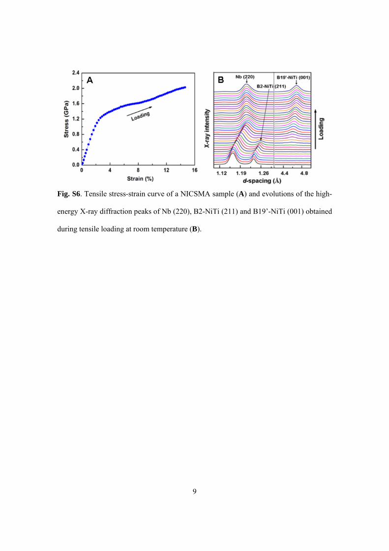
Fig. S6. Tensile stress-strain curve of a NICSMA sample (A) and evolutions of the high-
energy X-ray diffraction peaks of Nb (220), B2-NiTi (211) and B19’-NiTi (001) obtained
during tensile loading at room temperature (B).

10
Fig. S7. Scanning transmission electron microscopy images of a cross-section (A) and a
longitudinal-section (B) of a NICSMA wire (bright regions: Nb nanowires; dark regions:
NiTi matrix).
Note: The ribbon-shaped Nb nanowires are 3−20 nm in thickness, 20−200 nm in width,
and are well dispersed and fully aligned in the NiTi matrix along the wire axial direction.

11
Fig. S8. Tensile stress-strain curve of a NICSMA sample (A) and evolutions of the high-
energy X-ray diffraction peaks of Nb (220), B2-NiTi (211) and B19’-NiTi (001) during
tensile loading at 180 °C (B).
Note: It is seen in B that the B2-NiTi matrix survived the entire deformation to 15.5% of
global strain without transforming to the B19’ martensite at 180°C. This is because the
test temperature is higher than the critical temperature at which the critical stress for
SIMT equals that for plastic deformation of the austenite (26). Through tensile testing of
the NISCMA, the critical temperature for SIMT in the NiTi matrix is determined to be
~160 °C, above which dislocation slip occurs as the dominant mechanism of deformation.

12
Fig. S9. Comparison of strengths and elastic strains of ceramics, metals, polymers and
NICSMA.

13
Fig. S10. Cell adhesion of fibroblasts cultured on the surfaces of (A) NiTi, (B) Nb and (C)
NICSMA samples. Graph (D) shows the statistical cell number after four hours of culture
(*p < 0.05, mean + SD, N=3). The scale bars at the bottom of the images represent 100
μm.

14
Fig. S11. Methyl-thiazol-tetrazolium (MTT) assay for cell proliferation on NiTi, Nb and
NICSMA samples after 1, 3 and 5 days of culture (*p < 0.05, mean + SD, N=3).
Note: Nb is one of the most biocompatible metallic elements (24, 27, 28) and NiTi has
been used in medical treatment in many forms (29, 30). From Figs. S10 and S11, it can
be concluded that all the samples are well tolerated by fibroblast cells, with Nb and
NICSMA samples possessing relatively higher cell proliferation, indicating better cyto-
compatibility.

15
Fig. S12. Electrochemical characteristics of NICSMA. (A) Potentiodynamic anodic
polarization curves of NICSMA, NiTi and Nb samples in Hanks’ solution: 8.00 g/L NaCl,
0.14 g/L CaCl, 0.4 g/L KCl, 0.10 g/L MgCl2 • 6H2O, 0.10 g/L MgSO4•7H2O, 0.35 g/L
NaHCO3, 0.12 g/L Na2HPO4• 12H2O, 0.06 g/L KH2PO4 and 1.0 g/L Glucose (pH=7.4) at
310K. (B) Statistical analysis of the corrosion potential (Ecorr), breakdown potential (Ebr),
and (Ebr-Ecorr) (*p < 0.05, mean± SD, N =3) of the three materials.

References and Notes
1. M. F. Ashby, Materials Selection in Mechanical Design (Butterworth-Heinemann, City, 2005).
2. T. Saito et al., Multifunctional Alloys Obtained via a Dislocation-Free Plastic Deformation Mechanism. Science 300, 464 (2003). doi:10.1126/science.1081957 Medline
3. E. W. Wong, P. E. Sheehan, C. M. Lieber, Nanobeam Mechanics: Elasticity, Strength, and Toughness of Nanorods and Nanotubes. Science 277, 1971 (1997). doi:10.1126/science.277.5334.1971
4. T. Zhu, J. Li, Ultra-strength materials. Prog. Mater. Sci. 55, 710 (2010). doi:10.1016/j.pmatsci.2010.04.001
5. Y. Yue, P. Liu, Z. Zhang, X. Han, E. Ma, Approaching the theoretical elastic strain limit in copper nanowires. Nano Lett. 11, 3151 (2011). doi:10.1021/nl201233u Medline
6. G. Richter et al., Ultrahigh strength single crystalline nanowhiskers grown by physical vapor deposition. Nano Lett. 9, 3048 (2009). doi:10.1021/nl9015107 Medline
7. L. Tian et al., Approaching the ideal elastic limit of metallic glasses. Nat Commun. 3, 609 (2012). doi:10.1038/ncomms1619 Medline
8. K. Koziol et al., High-performance carbon nanotube fiber. Science 318, 1892 (2007); 10.1126/science.1147635. doi:10.1126/science.1147635 Medline
9. D. A. Walters et al., Elastic strain of freely suspended single-wall carbon nanotube ropes. Appl. Phys. Lett. 74, 3803 (1999). doi:10.1063/1.124185
10. Y. Dzenis, Materials science. Structural nanocomposites. Science 319, 419 (2008). doi:10.1126/science.1151434 Medline
11. P. Podsiadlo et al., Ultrastrong and stiff layered polymer nanocomposites. Science 318, 80 (2007). doi:10.1126/science.1143176 Medline
12. J. N. Coleman, U. Khan, Y. K. Gun'ko, Mechanical Reinforcement of Polymers Using Carbon Nanotubes. Adv. Mater. 18, 689 (2006). doi:10.1002/adma.200501851
13. L. Thilly et al., A new criterion for elasto-plastic transition in nanomaterials: Application to size and composite effects on Cu–Nb nanocomposite wires. Acta Mater. 57, 3157 (2009). doi:10.1016/j.actamat.2009.03.021
14. V. Vidal et al., Plasticity of nanostructured Cu–Nb-based wires: Strengthening mechanisms revealed by in situ deformation under neutrons. Scr. Mater. 60, 171 (2009). doi:10.1016/j.scriptamat.2008.09.032
15. K. Otsuka, C. M. Wayman, Eds., Shape Memory Materials (Cambridge Univ. Press, Cambridge, 1998).
16. K. Otsuka, X. Ren, Physical metallurgy of Ti–Ni-based shape memory alloys. Prog. Mater. Sci. 50, 511 (2005). doi:10.1016/j.pmatsci.2004.10.001

17. S. Ogata, J. Li, S. Yip, Ideal pure shear strength of aluminum and copper. Science 298, 807 (2002). doi:10.1126/science.1076652 Medline
18. M. Piao, S. Miyazaki, K. Otsuka, Mater. Trans. Jpn. Inst. Met. 33, 337 (1992).
19. See supplementary material on Science Online.
20. C. C. Aydıner, D. W. Brown, N. A. Mara, J. Almer, A. Misra, In situ x-ray investigation of freestanding nanoscale Cu–Nb multilayers under tensile load. Appl. Phys. Lett. 94, 031906 (2009). doi:10.1063/1.3074374
21. L. Thilly et al., Plasticity of multiscale nanofilamentary Cu∕Nb composite wires during in situ neutron diffraction: Codeformation and size effect. Appl. Phys. Lett. 88, 191906 (2006). doi:10.1063/1.2202720
22. C. Scheuerleina, U. Stuhr, L. Thilly, In situ neutron diffraction under tensile loading of powder-in-tube Cu∕Nb[sub 3]Sn composite wires: Effect of reaction heat treatment on texture, internal stress state, and load transfer. Appl. Phys. Lett. 91, 042503 (2007). doi:10.1063/1.2766685
23. M. Niinomi, M. Nakai, Titanium-Based Biomaterials for Preventing Stress Shielding between Implant Devices and Bone. Int. J. Biomater. 2011, 1 (2011). doi:10.1155/2011/836587
24. M. Niinomi, Recent metallic materials for biomedical applications. Metall. Mater. Trans. A Phys. Metall. Mater. Sci. 33, 477 (2002). doi:10.1007/s11661-002-0109-2
25. D. C. Hofmann et al., Designing metallic glass matrix composites with high toughness and tensile ductility. Nature 451, 1085 (2008). doi:10.1038/nature06598 Medline
26. Y. Liu, H. Xiang, Apparent modulus of elasticity of near-equiatomic NiTi. J. Alloy. Comp. 270, 154 (1998). doi:10.1016/S0925-8388(98)00500-3
27. H. Matsuno, A. Yokoyama, F. Watari, M. Uo, T. Kawasaki, Biocompatibility and osteogenesis of refractory metal implants, titanium, hafnium, niobium, tantalum and rhenium. Biomaterials 22, 1253 (2001). doi:10.1016/S0142-9612(00)00275-1 Medline
28. E. Eisenbarth, D. Velten, M. Müller, R. Thull, J. Breme, Biocompatibility of beta-stabilizing elements of titanium alloys. Biomaterials 25, 5705 (2004). doi:10.1016/j.biomaterials.2004.01.021 Medline
29. T. Duerig, A. Pelton, D. Stockel, An overview of nitinol medical applications. Mater. Sci. Eng. A 273-275, 149 (1999). doi:10.1016/S0921-5093(99)00294-4
30. D. Stoeckel, Nitinol medical devices and implants. Minim. Invasive Ther. Allied Technol. 9, 81 (2000). doi:10.3109/13645700009063054