a single-phase buck-boost pfc converter with output-voltage, ripple-reducing operation
TRANSCRIPT
A Single-Phase Buck-Boost PFC Converter with Output-Voltage, Ripple-Reducing
Operation
SHIN-ICHI MOTEGI, and AKESHI MAEDATokyo Denki University, Japan
SUMMARY
This paper describes a new single-phase buck-boost
power-factor-correction (PFC) converter with output-volt-
age, ripple reducing operation. The converter consists of a
conventional buck-boost PFC converter and an additional
switch to obtain a freewheeling mode of the dc inductor
current, and is operated by two modulators. The first modu-
lator controls the buck-boost switch to obtain PFC. The
other modulator controls the square value of the instanta-
neous dc inductor current to perform the output-voltage-
ripple-reducing operation. In the two modulations, the time
integral value of the input and output currents in each
modulation period are controlled directly and indirectly,
respectively. Thus, modulation errors or undesirable distor-
tions of the input current and output voltage ripple are
eliminated even if the dc inductor current produces large
ripple in a low-frequency range. The theories and combina-
tion techniques for the two modulators, implementation,
and experimental results are described. © 1998 Scripta
Technica, Electr Eng Jpn, 126(2): 56�70, 1999
Key words: Buck-boost converters; high power fac-
tor output voltage ripple reduction; pulse space modulation;
input�output power balance.
1. Introduction
A single-phase high-power-factor converter is indis-
pensable for home air conditioners and medical treatment
equipment used in places where three-phase power supplies
cannot be obtained. However, its input power contains a
frequency component twice the source frequency, and
many ripples of dc-side output voltage and current occur
due to that component and this can be regarded as a difficult
point in the single-phase high-power-factor converter
which did not exist in the three-phase converter. Since these
output voltage ripples of the converter exert negative ef-
fects, for example, distorting the ac output voltage of the
inverter connected on the dc side, these ripples are reduced
usually by inserting a relatively large-capacity smoothing
capacitor at the output terminal of the converter. However,
the use of a large-capacity capacitor not only has the disad-
vantage that its cost, dimension, and weight will increase
but also the necessity of applying the electrolytic capacitor
which requires regular exchange. Accordingly, for the
aforementioned problems, methods for reducing the output
voltage ripples (such as the methods of providing additional
circuits to the main circuit [1�5] and the method of devising
input current reference [6]) have been reported centered
around the voltage-source converters. A method for dealing
with the same ripples on the side of the inverter connected
as a load but not for reducing the output voltage ripples on
the converter side has also been proposed [7].
On the other hand, the authors and others have re-
ported that the single-phase buck-boost converter can be
operated with a sufficiently high power factor by operating
it in current continuous mode [8]. Moreover, we have also
reported that by providing and properly controlling a re-
verse-blocking switch connected in parallel with the dc
inductor of the converter, the reduction of the output voltage
ripples is also possible in addition to the high-power-factor
operation on the input side [9]. In these high-power-factor
converters, the modulation (pulse space modulation) is
performed so that the area of the pulse current which is the
modulated wave is made agreeing with (proportional to) the
reference for every modulation period. The original form
of this pulse space modulation has been proposed in Ref.
10 using a single-edge carrier signal of single polarity; and
the results of the authors and others are that its concrete
function and theoretical basis are clarified and the practical
activities in various fields including the reducing control of
the output voltage ripples are demonstrated, such as the
application to various converters of not only single-phase
CCC0424-7760/99/020056-15
© 1998 Scripta Technica
Electrical Engineering in Japan, Vol. 126, No. 2, 1999Translated from Denki Gakkai Ronbunshi, Vol. 117-D, No. 7, July 1997, pp. 846�855
56
and buck-boost type [11, 12] but also three-phase and
voltage-source type [13, 14] by developing a simple gen-
eration method of single/double polarity double-edge car-
ries and so forth [9, 11]. Moreover, its usefulness has also
been confirmed in Refs. 15 to 20. This pulse space modu-
lation is a modulation scheme in which the distortion of the
input current due to the ripples will not occur by adopting
the improved carries while the modulated wave is section-
ally integrated and generated even in the case where the
ripples exist in the modulated wave such as the dc output
current of voltage of voltage-source converter or the dc
(inductor) current-source converter.
However, in the reducing control of the output volt-
age ripples proposed previously by us [9], imbalance of the
input and output powers occurs easily, and the unnecessary
rise (rise of power device current) and the deficiency (ob-
struction to output-voltage-ripple-reducing operation) of
the dc inductor current due to that imbalance remain as
problems. With respect to this, we have proposed a simple
method in which by properly controlling the instantaneous
power of the dc inductor or the square instantaneous value
of the current such that the low-frequency components of
the output power ripples will become zero, the reduction of
the output voltage ripples (low-frequency components) and
the balance implementation of the input and output powers
can be realized simultaneously [21]. However, since the
effect of the internal resistance of the dc inductor on the
instantaneous power is neglected even in this control, a
small low-frequency ripple voltage (double frequency of
source frequency) has remained in the output voltage. Ac-
cordingly, we will propose in this paper an improved out-
put-voltage-ripple-reducing control considering the
internal resistance of the dc inductor. By using this control,
it is possible to remove, almost completely, the ac compo-
nent of double frequency from the instantaneous value of
the output voltage; and, moreover, it is learned that the
capacitance of the dc filter capacitor can be reduced to about
1/500 compared to the case of not using this control. Thus,
the miniaturization of this capacitor and, moreover, the
maintenance-free implementation due to the application of
the film capacitor can be expected.
On the other hand, even if the proposed improved
control is completely implemented, the low-frequency rip-
ples will remain in the output power when there exists a
distortion in the source voltage. After studying the effect of
this source voltage distortion on the output voltage ripples,
no effect of the extent which might be an obstacle in
practice is seen, and so it is learned that the proposed control
can be sufficiently offered for practical use. We will also
touch on this point in the following.
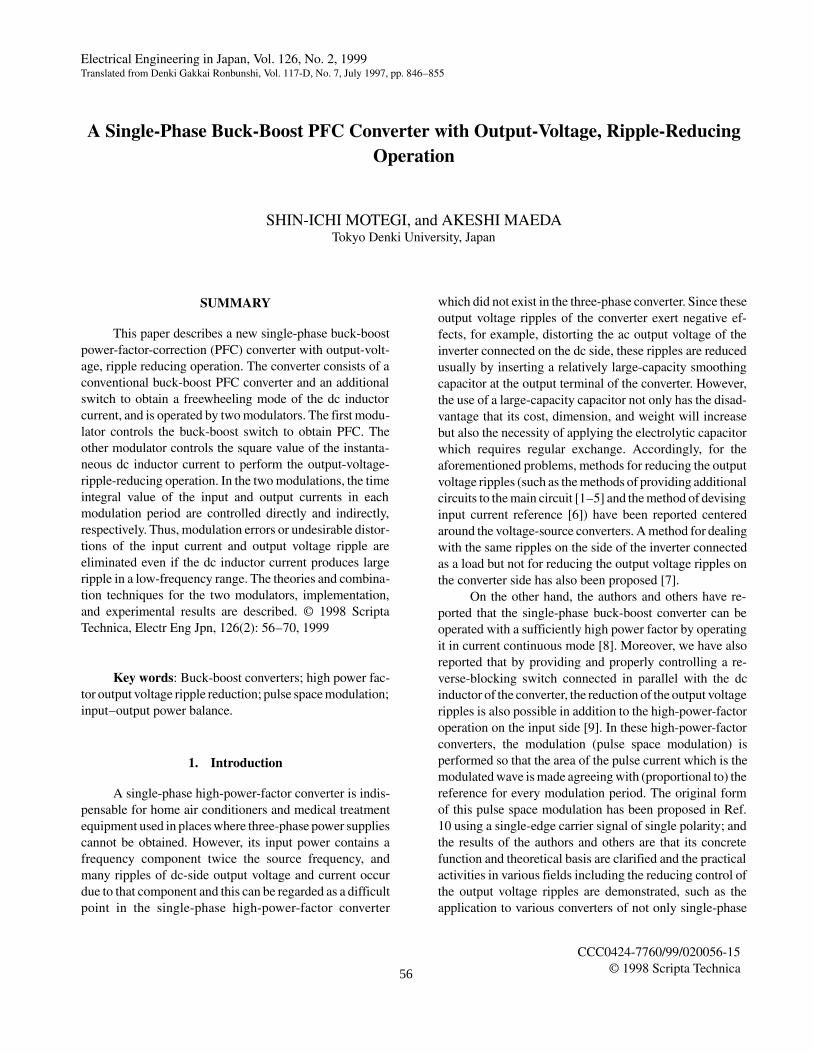
2. Configuration and Operation of Main Circuit
2.1 Configuration of main circuit
The single-phase buck-boost converter shown in Fig.
1 has the distinctive feature that a switch for dc inductor
current freewheeling (SWF, DF) is newly added to the
conventional constituting elements of single-phase source,
single-phase diode bridge (D1 to D4), harmonic filter (Lf,
Cf), buck-boost switch SWF, buck-boost dc inductor Ld,
buck-boost dc diode DO, dc filter capacitor CO, and load
resistor RO.
2.2 Operation of main circuit
Depending on the operation scheme, the buck-boost
converter can be roughly divided into the current intermit-
tent scheme in which it is operated by intermitting the dc
inductor current for all modulation periods and the current
continuous scheme in which it is operated by always main-
taining the current. In the case of the current intermittent
scheme, there are advantages such as that the modulator is
simple and the inductance of the dc inductor can be made
smaller; however, since the inductor current becomes a
pulsed triangular wave of high crest value and the losses
due to the inductance and switching devices become large,
this scheme has the disadvantage that it is limited to small-
capacity use. In the current continuous scheme, on the other
hand, large-capacity implementation is possible compared
with the current intermittent scheme; however, since the
inductance current will pulsate largely, errors will occur in
the modulation of the input current when the inductance of
the dc inductor is not sufficiently large. In this case, suffi-
cient input current modulation cannot be realized unless the
pulsation of the inductor current itself is reduced or the
current is detected and performed with some measures in
the modulation method. Accordingly, in this converter, by
adopting the pulse space modulation which is a modulation
Fig. 1. Proposed single-phase buck-boost PFC
converter system.
57
method for solving the above-mentioned problems, the
increase of the conversion capacity is devised while the
modulation of the input current under pulsating current is
made a relatively simple one. Besides, the buck-boost con-
verter can step up (boost) the output voltage higher or step
down (buck) lower than that; and so various applications
reviving this distinctive feature can be expected.
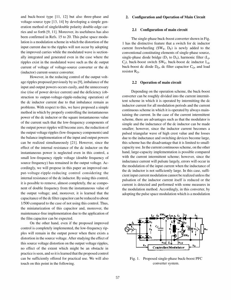
2.3 Operating modes of main circuit operation
With respect to the dc inductor Ld, the operation of
this buck-boost converter can be divided into the following
four operating modes (circuit states) depending on its con-
nection state with the source and load.
· Mode I: Ld is connected to source side (SWS: ON,
SWF: OFF)
· Mode II: Ld is connected to load side (SWS: OFF,
SWF: OFF)
· Mode III: Ld is not connected to either side and the
inductor current freewheels (SWS: OFF, SWF:
ON)
· Mode IV: The current of Ld is zero (the dc inductor
is used under current intermittent operation; this
mode will be excluded in the proposed scheme)
Figure 2 shows the circuit states in these operating modes,
and the source diode bridge and so forth of Fig. 1 are
omitted.
From the above, since the mode in which the dc
inductor is connected to the source side is Mode I only, the
sinusoidal implementation of the input current, that is,
high-power-factor operation, can be realized by properly
controlling the period of this mode for every modulation
period as described later, by using the pulse space modula-
tion. Similarly, by properly controlling the period of Mode
II in which the dc inductor is connected to the load side, the
ripple-reducing operation of the load-side output voltage
can be realized. However, in order to properly control the
periods of these operating modes while satisfying the above
conditions (high-power-factor operation and ripple-reduc-
ing operation) simultaneously, it is necessary to provide the
mode in which the dc inductor is connected neither to the
input side nor the load side, namely, the freewheeling mode
(Mode III) of the dc inductor current proposed by us.
3. Principles of Control and Modulation
The controller/modulator of the proposed single-
phase buck-boost high-power-factor converter with output-
voltage-ripple-reducing operation consist of a modulator
(pulse space modulator) for making the input current a
sinusoidal wave in phase with the source voltage and an
output-voltage-ripple-reducing controller for reducing the
low-frequency ripples of the output voltage. In the follow-
ing, the principles of controller and modulator are ex-
plained by separating them into the pulse space modulator
and output-voltage-ripple-reducing controller.
3.1 Input-side high-power-factor control
In this high-power-factor converter, keeping the
miniaturization of the dc inductor in mind, the pulse space
modulation is adopted for avoiding the occurrence of the
input current distortion due to the large ripples of the
inductor current that occur at the time of miniaturization
(low-inductance implementation). Moreover, in addition to
coping with the measure by control and modulation
adopted in the proposed scheme, a method has also been
proposed in which an LC-parallel resonant circuit for filter-
ing the double-frequency component of the source fre-
quency which is the main component of the pulsating
current, is inserted in the main circuit [22]. In the latter, the
pulsation itself can be suppressed and the small-size light-
weight implementation of the equipment becomes possible
compared with the conventional scheme using a large-
capacity dc inductor; however, in the case of the proposed
scheme, since it is coped inside the controller/modulator,
further small-size light-weight implementation of the
equipment is possible even compared with the latter
method. In the following, we will introduce the details of
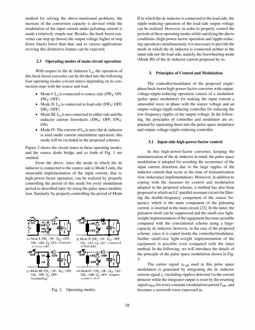
the principle of the pulse space modulation shown in Fig.
3.
The carrier signal nCAR used in this pulse space
modulation is generated by integrating the dc inductor
current signal iL (including ripples) detected via the current
detector while the integrator output is reset by the resetting
signal nRST for every constant (modulation) period TSW, and
becomes a sawtooth wave expressed asFig. 2. Operating modes.
58
On the other hand, as the area in each modulation
period of the buck-boost switch current iSW, that is, the
reference sB* of the sectionally integrated value sB, we use
the absolute value iB* of the input current reference iS
* in
phase with the source voltage multiplied by the modulation
period TSW:
Comparing these carrier signal nCAR and space refer-
ence sB* , the period of Mode I in which the dc inductor Ld
is connected to the source side is determined; and as shown
in the lower part of Fig. 3, Mode I is maintained from the
starting time t = tk of each modulation period to the time
t = tkg where the reference sB
* and the carrier signal nCAR
intersect. Therefore, the dc inductor current iL will flow to
the source side via the buck-boost switch SWS during this
period (TON; t = tk to t = tkg in Fig. 3). At this point, the area
sB of the switch current in each modulation period becomes
and agrees with the reference sB* . Besides, since the switch-
ing frequency component of the switch current iSW is fil-
tered by the harmonic filter (Lf, Cf), and its polarity is
reversed at every half period by the diode bridge and
becomes the input current iS, the average value in each
modulation period of the input current iS or the low-fre-
quency component of the input current iS will agree with
the input current reference iS*.
Moreover, the modulation period can be easily and
freely adjusted by changing the period of the resetting
signal nRST.
3.2 Output-voltage-ripple-reducing control
As described previously, as a scheme for removing
the low-frequency ripple of the output voltage in the single-
phase buck-boost high-power-factor converter, we have
proposed providing a freewheeling switch (SWF, DF) in
addition to the buck-boost switch SWS; however, in the
control scheme previously reported [9], since these two
switches are controlled by two independent current refer-
ences, there is the problem that imbalance between input
and output powers easily occurs. Accordingly, we have
proposed a method for reducing the output voltage ripples
by making the instantaneous value of the dc inductor power
and the ac component of the input power equal by properly
controlling the instantaneous value (LdiL2 /2) of the stored
energy of the dc inductor, that is, the square value of the
instantaneous inductor current (iL2), and thus indirectly per-
forming the control such that the low-frequency component
of the output power ripple will become zero (or the average
value in each modulation period is constant) [21]. In this
proposal, since the dc inductor current reference is com-
puted from the input current reference, the output-voltage-
ripple-reducing control becomes possible without the
occurrence of the imbalance between input and output
powers. However, since the consumed power of the internal
resistance of the dc inductor in that scheme is neglected, the
ripple component of that power is supplied from the load
side, and a pulsation of double source frequency will occur
in the instantaneous value of the output power; and so a
pulsating voltage of that frequency has barely remained in
the output voltage.
For improving this, we will propose in this paper an
improved output-voltage-ripple-reducing control in which
the instantaneous value of the pulsating power of the entire
dc inductor including the internal resistance of the dc
inductor is made equal to the ac component of the input
power. By using this control, the double-frequency ac com-
ponent can almost completely be removed from the instan-
taneous value of the output voltage. In the following, for
output-voltage-ripple reduction, the square-value reference
of the dc inductor current, (iL2)*, will be derived by separat-
ing it into the ac component (iL2)AC
* (abbreviated hereafter as
ac component) and the dc component (iL2)DC
* , excluding the
switching ripples.
Fig. 3. Principle of pulse space modulation.
(1)
(2)
(3)
59
This converter system is considered as ideal (exclud-
ing dc inductor Ld) and the losses of the switching devices
are neglected; and if pL is the instantaneous value of the
input power to the dc inductor Ld excluding the internal
resistance, pr is the instantaneous value of the consumed
power of the internal resistance rL of the dc inductor, and
pO is the instantaneous value of the output power, then the
instantaneous value ps of the input power can be expressed
as
Moreover, if the high-power-factor operation is carried out,
and the source voltage ns and current is are in-phase sinusoi-
dal waves [nS = Ö̀̀2Vs sin(wt), is = Ö̀̀2 Is sin(wt), w = 2pfs,fs is the source frequency), the instantaneous value ps of the
input power can be given as
Furthermore, the instantaneous value pO of the output
power, the instantaneous value pL of the dc inductor power,
and the instantaneous value pr of the consumed power of
the internal resistance can be expressed similarly by the sum
of the dc component and the ac component, respectively:
Now, from Eq. (4),
can be obtained and substituting this equation into Eqs. (5)
and (6) yields
Separating the above equation into the dc component
and the ac component yields
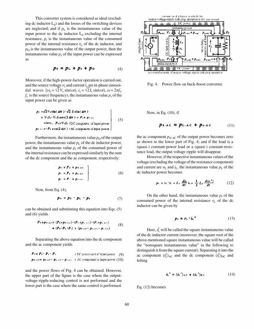
and the power flows of Fig. 4 can be obtained. However,
the upper part of the figure is the case where the output-
voltage-ripple-reducing control is not performed and the
lower part is the case where the same control is performed.
Now, in Eq. (10), if
the ac component pO-AC of the output power becomes zero
as shown in the lower part of Fig. 4; and if the load is a
(quasi-) constant-power load or a (quasi-) constant-resis-
tance load, the output voltage ripple will disappear.
However, if the respective instantaneous values of the
voltage (excluding the voltage of the resistance component)
and current are nL and iL, the instantaneous value pL of the
dc inductor power becomes
On the other hand, the instantaneous value pr of the
consumed power of the internal resistance rL of the dc
inductor can be given by
Here, iL2 will be called the square instantaneous value
of the dc inductor current (moreover, the square root of the
above-mentioned square instantaneous value will be called
the �nonsquare instantaneous value� in the following to
distinguish it from the square current). Separating it into the
ac component (iL2)AC and the dc component (iL
2)DC and
letting
Eq. (12) becomes
(10)
(4)
(5)
(6)
(7)
(8)
(9)
(11)
(12)
(13)
(14)
Fig. 4. Power flow on buck-boost converter.
60
Separating the above equation into the ac component
and the dc component yields
However, the dc component pL in the above equation is zero
in the steady state. Similarly, by substituting Eq. (14) into
Eq. (13) and separating it into the ac component and dc
component, the consumed power of the internal resistance
of the dc inductor becomes
Hence, when the ac component of the instantaneous
value of the output power, pO-AC = 0, is satisfied, the
following equation holds by substituting Eqs. (16) and (19)
into Eq. (11):
Hence, rewriting the left-hand side of the above equa-
tion using Eq. (5), we have
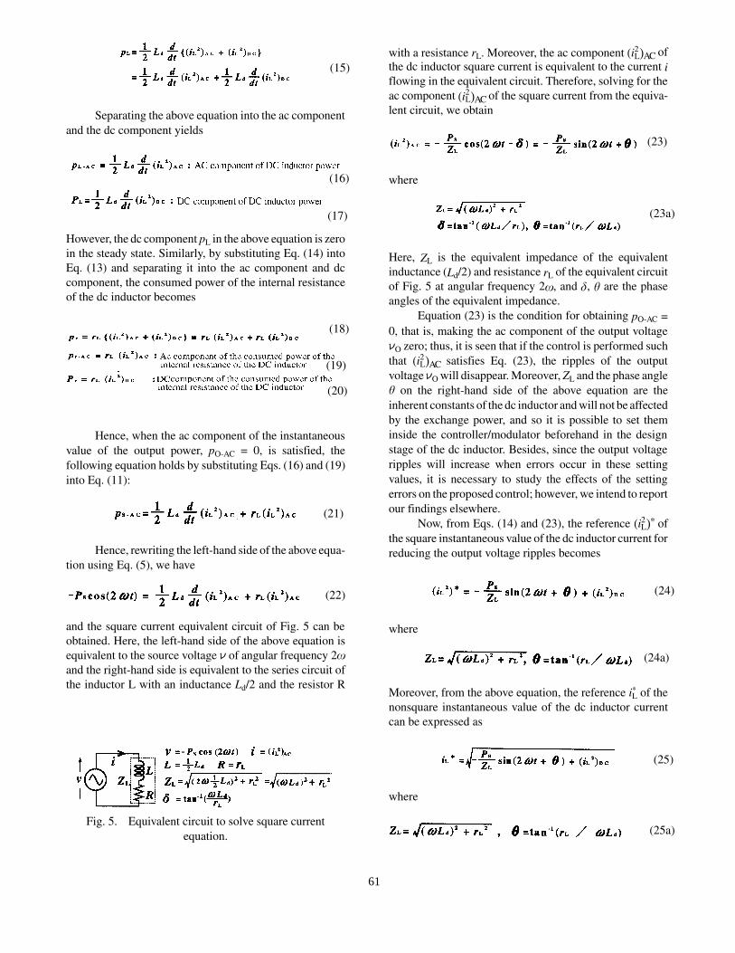
and the square current equivalent circuit of Fig. 5 can be
obtained. Here, the left-hand side of the above equation is
equivalent to the source voltage n of angular frequency 2wand the right-hand side is equivalent to the series circuit of
the inductor L with an inductance Ld/2 and the resistor R
with a resistance rL. Moreover, the ac component (iL2)AC of
the dc inductor square current is equivalent to the current i
flowing in the equivalent circuit. Therefore, solving for the
ac component (iL2)AC of the square current from the equiva-
lent circuit, we obtain
where
Here, ZL is the equivalent impedance of the equivalent
inductance (Ld/2) and resistance rL of the equivalent circuit
of Fig. 5 at angular frequency 2w, and d, q are the phase
angles of the equivalent impedance.
Equation (23) is the condition for obtaining pO-AC =
0, that is, making the ac component of the output voltage
nO zero; thus, it is seen that if the control is performed such
that (iL2)AC satisfies Eq. (23), the ripples of the output
voltage nO will disappear. Moreover, ZL and the phase angle
q on the right-hand side of the above equation are the
inherent constants of the dc inductor and will not be affected
by the exchange power, and so it is possible to set them
inside the controller/modulator beforehand in the design
stage of the dc inductor. Besides, since the output voltage
ripples will increase when errors occur in these setting
values, it is necessary to study the effects of the setting
errors on the proposed control; however, we intend to report
our findings elsewhere.
Now, from Eqs. (14) and (23), the reference (iL2)* of
the square instantaneous value of the dc inductor current for
reducing the output voltage ripples becomes
where
Moreover, from the above equation, the reference iL* of the
nonsquare instantaneous value of the dc inductor current
can be expressed as
where
(18)
(19)
(20)
(21)
(22)
(16)
(17)
(15)
(23)
(23a)
(24)
Fig. 5. Equivalent circuit to solve square current
equation.
(24a)
(25)
(25a)
61
However, the dc component (iL2)DC of the above ref-
erence is arbitrary in the range where there is no hindrance
to the output-voltage-ripple-reducing control; however,
when the loss due to the internal resistance rL of the dc
inductor is taken into account, it is desirable to make it the
minimum (optimal) value [let this be the dc component
reference (iL2)DC
* ] on satisfying the above-mentioned condi-
tion. In the following, we will derive the average value of
the square instantaneous value reference (iL2)* of the dc
inductor current during the source period, namely, the dc
component reference (iL2)DC
* .
At point A of the main circuit shown in Fig. 1, the
current equation is
Here, the low-frequency components (including the dc
component, abbreviated as low-frequency component in
the following) excluding switching ripples of the respective
currents will be expressed by adding �#� to the symbol of
the respective instantaneous values, as �iL#�; and when Eq.
(26) is written as the current equation in the low-frequency
region, it becomes
In the above equation, the low-frequency component iSW# of
the buck-boost switch current is modulated by the pulse
space modulation such that it is equal to the input current
reference iB* , and the low-frequency component iL
# of the dc
inductor current is controlled by the proposed ripple-reduc-
ing control such that it is equal to the dc inductor current
reference iL* expressed by Eq. (25). Moreover, by perform-
ing the ripple-reducing control, the low-frequency compo-
nent iD# of the buck-boost diode current is equal to the
average value IO of the output current and becomes constant
and smooth. Therefore, rewriting Eq. (27) from the above,
we obtain
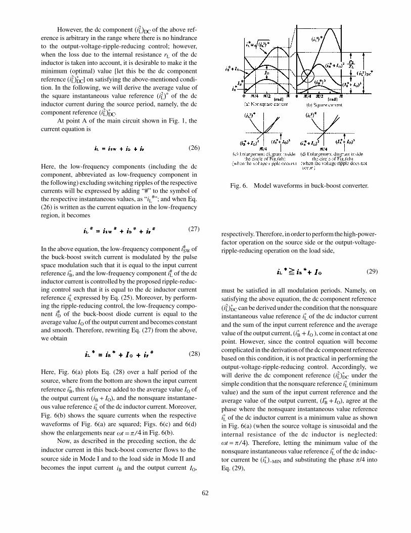
Here, Fig. 6(a) plots Eq. (28) over a half period of the
source, where from the bottom are shown the input current
reference iB* , this reference added to the average value IO of
the output current (iB + IO), and the nonsquare instantane-
ous value reference iL* of the dc inductor current. Moreover,
Fig. 6(b) shows the square currents when the respective
waveforms of Fig. 6(a) are squared; Figs. 6(c) and 6(d)
show the enlargements near wt = p / 4 in Fig. 6(b).
Now, as described in the preceding section, the dc
inductor current in this buck-boost converter flows to the
source side in Mode I and to the load side in Mode II and
becomes the input current iB and the output current IO,
respectively. Therefore, in order to perform the high-power-
factor operation on the source side or the output-voltage-
ripple-reducing operation on the load side,
must be satisfied in all modulation periods. Namely, on
satisfying the above equation, the dc component reference
(iL2)DC
* can be derived under the condition that the nonsquare
instantaneous value reference iL* of the dc inductor current
and the sum of the input current reference and the average
value of the output current, (iB* + IO ), come in contact at one
point. However, since the control equation will become
complicated in the derivation of the dc component reference
based on this condition, it is not practical in performing the
output-voltage-ripple-reducing control. Accordingly, we
will derive the dc component reference (iL2)DC
* under the
simple condition that the nonsquare reference iL* (minimum
value) and the sum of the input current reference and the
average value of the output current, (IB* + IO), agree at the
phase where the nonsquare instantaneous value reference
iL* of the dc inductor current is a minimum value as shown
in Fig. 6(a) (when the source voltage is sinusoidal and the
internal resistance of the dc inductor is neglected:
wt = p / 4). Therefore, letting the minimum value of the
nonsquare instantaneous value reference iL* of the dc induc-
tor current be (iL*)-MIN and substituting the phase p/4 into
Eq. (29),
(26)
(27)
(28)
Fig. 6. Model waveforms in buck-boost converter.
(29)
62
can be obtained. Here, squaring both sides of Eq. (30) yields
Moreover, since ((iL*)
wMIN)2 = (iL2)wMIN
* , the above equation
is
Furthermore, from Eq. (24), the minimum value (iL2)
wMIN* of
the square instantaneous value reference of the dc inductor
current can be expressed as
Here, substituting Eq. (33) into the left-hand side of Eq. (32)
and rearranging for (iL2)DC,
can be obtained. However, if we let (iL2)DC given by the
above equation be the dc component reference (iL2)DC
* of
(iL2)*, the period
will be formed near wt = p /4 as shown in Fig. 6(c), and it
is necessary to avoid this because the output-voltage-ripple-
reducing operation will be hindered a little. As shown in the
following equation, we have multiplied the entire right-
hand side of Eq. (34) by a constant KDC of over 1 (setting
in such a way that the output voltage ripple will not occur
at rated load) and let it be the dc component reference
(iL2)DC
* , and the output-voltage-ripple-reducing operation is
carried out by letting this reference have a margin as shown
in Fig. 6(d).
This is the dc component reference (iL2)DC
* of (iL2)* for
performing the output-voltage-ripple reduction while mini-
mizing the loss due to the internal resistance rL of the dc
inductor.
By the above theoretical analysis, the average value
of the optimal (minimum) square instantaneous value ref-
erence (iL2)* of the dc inductor current in the source period,
namely, the dc component reference (iL2)DC
* , can be ob-
tained; and from this and Eq. (24), the reference (iL2)* of the
square instantaneous value of the dc inductor current for
ripple reduction can be obtained (see Fig. 6). Therefore, if
the control is performed such that the square value iL2 of the
dc inductor current agrees with the reference (iL2)*, the
output voltage ripples can be eliminated theoretically.
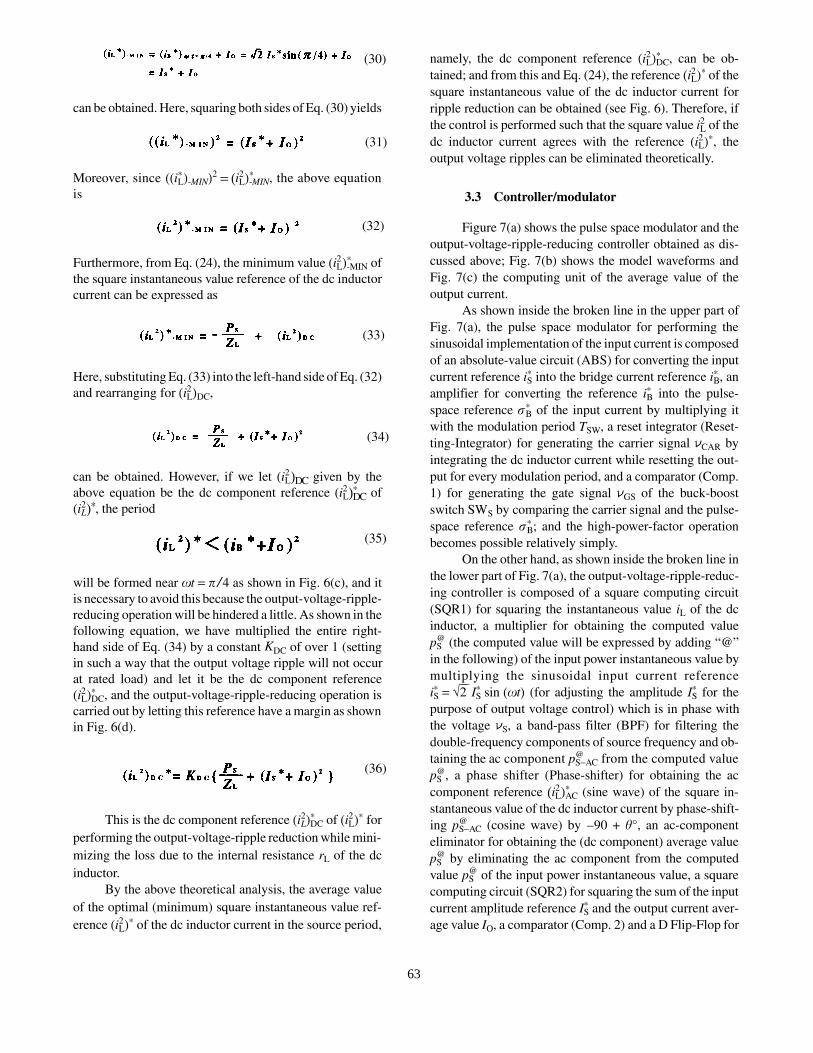
3.3 Controller/modulator
Figure 7(a) shows the pulse space modulator and the
output-voltage-ripple-reducing controller obtained as dis-
cussed above; Fig. 7(b) shows the model waveforms and
Fig. 7(c) the computing unit of the average value of the
output current.
As shown inside the broken line in the upper part of
Fig. 7(a), the pulse space modulator for performing the
sinusoidal implementation of the input current is composed
of an absolute-value circuit (ABS) for converting the input
current reference iS* into the bridge current reference iB
* , an
amplifier for converting the reference iB* into the pulse-
space reference sB* of the input current by multiplying it
with the modulation period TSW, a reset integrator (Reset-
ting-Integrator) for generating the carrier signal nCAR by
integrating the dc inductor current while resetting the out-
put for every modulation period, and a comparator (Comp.
1) for generating the gate signal nGS of the buck-boost
switch SWS by comparing the carrier signal and the pulse-
space reference sB* ; and the high-power-factor operation
becomes possible relatively simply.
On the other hand, as shown inside the broken line in
the lower part of Fig. 7(a), the output-voltage-ripple-reduc-
ing controller is composed of a square computing circuit
(SQR1) for squaring the instantaneous value iL of the dc
inductor, a multiplier for obtaining the computed value
pS@ (the computed value will be expressed by adding �@�
in the following) of the input power instantaneous value by
multiplying the sinusoidal input current reference
iS* = Ö̀̀2 IS
* sin (wt) (for adjusting the amplitude IS* for the
purpose of output voltage control) which is in phase with
the voltage nS, a band-pass filter (BPF) for filtering the
double-frequency components of source frequency and ob-
taining the ac component pS-AC@ from the computed value
pS@, a phase shifter (Phase-shifter) for obtaining the ac
component reference (iL2)AC* (sine wave) of the square in-
stantaneous value of the dc inductor current by phase-shift-
ing pS-AC@ (cosine wave) by �90 + q°, an ac-component
eliminator for obtaining the (dc component) average value
pS@ by eliminating the ac component from the computed
value pS@ of the input power instantaneous value, a square
computing circuit (SQR2) for squaring the sum of the input
current amplitude reference IS* and the output current aver-
age value IO, a comparator (Comp. 2) and a D Flip-Flop for
(30)
(31)
(32)
(33)
(34)
(35)
(36)
63
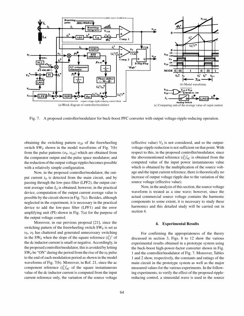
obtaining the switching pattern nGF of the freewheeling
switch SWF shown in the model waveforms of Fig. 7(b)
from the pulse patterns (nF, nGS) which are obtained from
the comparator output and the pulse space modulator; and
the reduction of the output voltage ripples becomes possible
with a relatively simple configuration.
Now, in the proposed controller/modulator, the out-
put current iO is detected from the main circuit, and by
passing through the low-pass filter (LPF2), the output cur-
rent average value IO is obtained; however, in the practical
device, computation of the output current average value is
possible by the circuit shown in Fig. 7(c). Besides, although
neglected in the experiment, it is necessary in the practical
device to add the low-pass filter (LPF1) and the error
amplifying unit (PI) shown in Fig. 7(a) for the purpose of
the output voltage control.
Moreover, in our previous proposal [21], since the
switching pattern of the freewheeling switch SWF is set as
nF, nF has chattered and generated unnecessary switching
in the SWF when the slope of the square reference (iL2)* of
the dc inductor current is small or negative. Accordingly, in
the proposed controller/modulator, this is avoided by letting
SWF be �ON� during the period from the rise of the nF pulse
to the end of each modulation period as shown in the model
waveforms of Fig. 7(b). Moreover, in Ref. 21, since the ac
component reference (iL2)AC
* of the square instantaneous
value of the dc inductor current is computed from the input
current reference only, the variation of the source voltage
(effective value) VS is not considered, and so the output-
voltage-ripple reduction is not sufficient on that point. With
respect to this, in the proposed controller/modulator, since
the abovementioned reference (iL2)AC
* is obtained from the
computed value of the input power instantaneous value
which is obtained by the multiplication of the source volt-
age and the input current reference, there is theoretically no
increase of output voltage ripple due to the variation of the
source voltage (effective value).
Now, in the analysis of this section, the source voltage
waveform is treated as a sine wave; however, since the
actual commercial source voltage contains the harmonic
components to some extent, it is necessary to study these
harmonics and this detailed study will be carried out in
section 4.
4. Experimental Results
For confirming the appropriateness of the theory
discussed in section 3, Figs. 8 to 12 show the various
experimental results obtained in a prototype system using
the buck-boost high-power-factor converter shown in Fig.
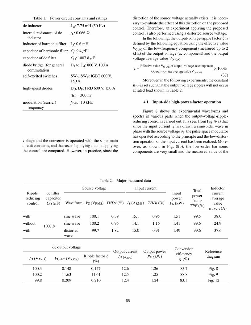
1 and the controller/modulator of Fig. 7. Moreover, Tables
1 and 2 show, respectively, the constants and ratings of the
main circuit in the prototype system as well as the major
measured values for the various experiments. In the follow-
ing experiments, to verify the effect of the proposed ripple-
reducing control, a sinusoidal wave is used in the source
Fig. 7. A proposed controller/modulator for buck-boost PFC converter with output voltage-ripple-reducing operation.
64
voltage and the converter is operated with the same main
circuit constants, and the case of applying and not applying
the control are compared. However, in practice, since the
distortion of the source voltage actually exists, it is neces-
sary to evaluate the effect of this distortion on the proposed
control. Therefore, an experiment applying the proposed
control is also performed using a distorted source voltage.
In the following, the output-voltage-ripple factor x is
defined by the following equation using the effective value
VO-AC of the low-frequency component (measured up to 2
kHz) of the output voltage (ac component) and the output
voltage average value VO-AVG:
x = Effective value VO-AC of output-voltage ac component
Output-voltage average value VO-AVG
´ 100%
(37)
Moreover, in the following experiments, the constant
KDC is set such that the output voltage ripples will not occur
at rated load shown in Table 2.
4.1 Input-side high-power-factor operation
Figure 8 shows the experimental waveforms and
spectra in various parts when the output-voltage-ripple-
reducing control is carried out. It is seen from Fig. 8(a) that
since the input current iS has drawn a sinusoidal wave in
phase with the source voltage nS, the pulse space modulator
has operated according to the principle and the low-distor-
tion operation of the input current has been realized. More-
over, as shown in Fig. 8(b), the low-order harmonic
components are very small and the measured value of the
Table 2. Major measured data
Ripple
reducing
control
dc filter
capacitor
CO (mF)
Source voltage Input current
Input
power
PS (kW)
Total
power
factor
TPF (%)
Inductor
current
average
value
iL-AVG (A)
Waveform VS (VRMS) THDv (%) IS (ARMS) THDi (%)
with
1007.8
sine wave 100.1 0.39 15.1 0.95 1.51 99.5 38.0
without sine wave 100.2 0.96 14.1 1.16 1.41 99.6 24.9
with distorted
wave
99.7 1.82 15.0 0.91 1.49 99.6 37.6
Table 1. Power circuit constants and ratings
dc inductor Ld: 7.75 mH (50 Hz)
internal resistance of dc
inductor
rL: 0.066 W
inductor of harmonic filter Lf: 0.6 mH
capacitor of harmonic filter Cf: 9.4 mF
capacitor of dc filter CO: 1007.8 mF
diode bridge (for general
commutation)
D1 to D4: 800 V, 100 A
self-excited switches SWS, SWF: IGBT 600 V,
150 A
high-speed diodes DO, DF: FRD 600 V, 150 A
(trr = 300 ns)
modulation (carrier)
frequency
fCAR: 10 kHz
dc output voltageOutput current
IO (AAVG)
Output power
PO (kW)
Conversion
efficiency
h (%)
Reference
diagramVO (VAVG) VO-AC (VRMS)
Ripple factor x(%)
100.3 0.148 0.147 12.6 1.26 83.7 Fig. 8
100.2 11.63 11.61 12.5 1.25 88.8 Fig. 9
99.8 0.209 0.210 12.4 1.24 83.1 Fig. 12
65
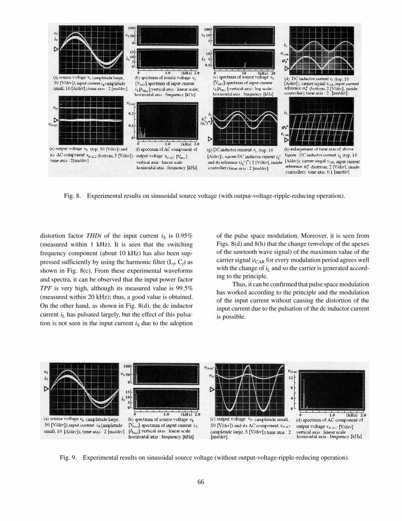
distortion factor THDi of the input current iS is 0.95%
(measured within 1 kHz). It is seen that the switching
frequency component (about 10 kHz) has also been sup-
pressed sufficiently by using the harmonic filter (Lf, Cf) as
shown in Fig. 8(c). From these experimental waveforms
and spectra, it can be observed that the input power factor
TPF is very high, although its measured value is 99.5%
(measured within 20 kHz); thus, a good value is obtained.
On the other hand, as shown in Fig. 8(d), the dc inductor
current iL has pulsated largely, but the effect of this pulsa-
tion is not seen in the input current iS due to the adoption
of the pulse space modulation. Moreover, it is seen from
Figs. 8(d) and 8(h) that the change (envelope of the apexes
of the sawtooth wave signal) of the maximum value of the
carrier signal nCAR for every modulation period agrees well
with the change of iL and so the carrier is generated accord-
ing to the principle.
Thus, it can be confirmed that pulse space modulation
has worked according to the principle and the modulation
of the input current without causing the distortion of the
input current due to the pulsation of the dc inductor current
is possible.
Fig. 8. Experimental results on sinusoidal source voltage (with output-voltage-ripple-reducing operation).
Fig. 9. Experimental results on sinusoidal source voltage (without output-voltage-ripple-reducing operation).
66
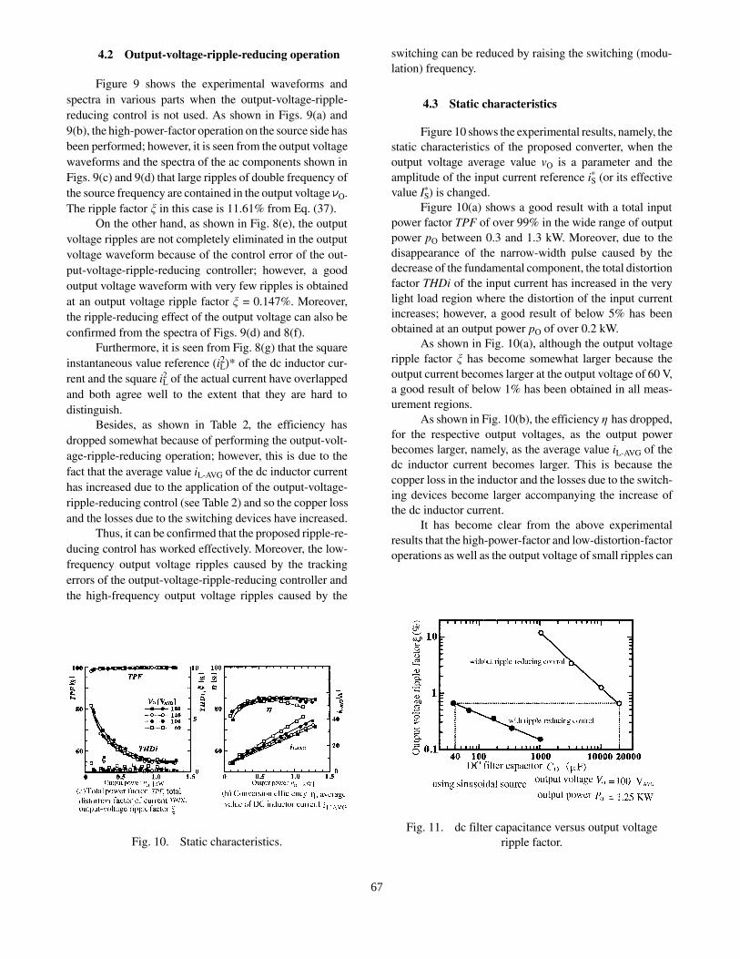
4.2 Output-voltage-ripple-reducing operation
Figure 9 shows the experimental waveforms and
spectra in various parts when the output-voltage-ripple-
reducing control is not used. As shown in Figs. 9(a) and
9(b), the high-power-factor operation on the source side has
been performed; however, it is seen from the output voltage
waveforms and the spectra of the ac components shown in
Figs. 9(c) and 9(d) that large ripples of double frequency of
the source frequency are contained in the output voltage nO.
The ripple factor x in this case is 11.61% from Eq. (37).
On the other hand, as shown in Fig. 8(e), the output
voltage ripples are not completely eliminated in the output
voltage waveform because of the control error of the out-
put-voltage-ripple-reducing controller; however, a good
output voltage waveform with very few ripples is obtained
at an output voltage ripple factor x = 0.147%. Moreover,
the ripple-reducing effect of the output voltage can also be
confirmed from the spectra of Figs. 9(d) and 8(f).
Furthermore, it is seen from Fig. 8(g) that the square
instantaneous value reference (iL2)* of the dc inductor cur-
rent and the square iL2 of the actual current have overlapped
and both agree well to the extent that they are hard to
distinguish.
Besides, as shown in Table 2, the efficiency has
dropped somewhat because of performing the output-volt-
age-ripple-reducing operation; however, this is due to the
fact that the average value iL-AVG of the dc inductor current
has increased due to the application of the output-voltage-
ripple-reducing control (see Table 2) and so the copper loss
and the losses due to the switching devices have increased.
Thus, it can be confirmed that the proposed ripple-re-
ducing control has worked effectively. Moreover, the low-
frequency output voltage ripples caused by the tracking
errors of the output-voltage-ripple-reducing controller and
the high-frequency output voltage ripples caused by the
switching can be reduced by raising the switching (modu-
lation) frequency.
4.3 Static characteristics
Figure 10 shows the experimental results, namely, the
static characteristics of the proposed converter, when the
output voltage average value vO is a parameter and the
amplitude of the input current reference iS* (or its effective
value IS*) is changed.
Figure 10(a) shows a good result with a total input
power factor TPF of over 99% in the wide range of output
power pO between 0.3 and 1.3 kW. Moreover, due to the
disappearance of the narrow-width pulse caused by the
decrease of the fundamental component, the total distortion
factor THDi of the input current has increased in the very
light load region where the distortion of the input current
increases; however, a good result of below 5% has been
obtained at an output power pO of over 0.2 kW.
As shown in Fig. 10(a), although the output voltage
ripple factor x has become somewhat larger because the
output current becomes larger at the output voltage of 60 V,
a good result of below 1% has been obtained in all meas-
urement regions.
As shown in Fig. 10(b), the efficiency h has dropped,
for the respective output voltages, as the output power
becomes larger, namely, as the average value iL-AVG of the
dc inductor current becomes larger. This is because the
copper loss in the inductor and the losses due to the switch-
ing devices become larger accompanying the increase of
the dc inductor current.
It has become clear from the above experimental
results that the high-power-factor and low-distortion-factor
operations as well as the output voltage of small ripples can
Fig. 10. Static characteristics.
Fig. 11. dc filter capacitance versus output voltage
ripple factor.
67
be obtained in the proposed converter with output-voltage-
ripple-reducing operation, which can withstand practical
use in the output voltage range from buck to boost (between
60 and 180 V in the experiments) and the considerably wide
range of output power (between 0.3 and 1.3 kW in the
experiments).
4.4 Reduction of the capacitance of dc filter
capacitor
For evaluating the ripple-reducing function of the
proposed converter with output-voltage-ripple-reducing
operation, we have carried out experiments by changing the
capacitance of the dc filter capacitor. In this case, the source
voltage is a sinusoidal wave, the output voltage nO is 100
VAVG, and the output power pO is 1.25 kW.
Figure 11 shows the output voltage ripple factor xwith respect to the capacitance CO of the dc filter capacitor
for the cases of performing and not performing the ripple-
reducing control. As seen from the fact that the ripple factor
in the case when the ripple-reducing control is used with a
capacitance of about CO = 40 mF and the ripple factor in the
case when the ripple-reducing control is not used with a
capacitance of about CO = 20,000 mF are about the same, it
is possible to reduce the capacitance of the dc filter capaci-
tor from 20,000 mF to 40 mF by using the output-voltage-
ripple-reducing control, and so the reduction factor of the
capacitance in this case is 1/500. Therefore, the capacitance
of the dc filter capacitor can be greatly reduced and the
small-size light-weight implementation of the dc filter ca-
pacitor and, moreover, the maintenance-free implementa-
tion without using chemical capacitors can be expected.
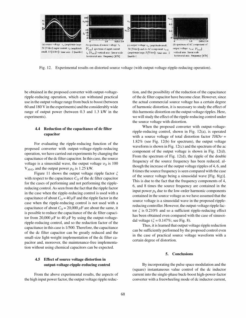
4.5 Effect of source voltage distortion in
output-voltage-ripple-reducing control
From the above experimental results, the aspects of
the high input power factor, the output voltage ripple reduc-
tion, and the possibility of the reduction of the capacitance
of the dc filter capacitor have become clear. However, since
the actual commercial source voltage has a certain degree
of harmonic distortion, it is necessary to study the effect of
this harmonic distortion on the output voltage ripples. Here,
we will study the effect of the ripple-reducing control under
the source voltage with distortion.
When the proposed converter with output-voltage-
ripple-reducing control, shown in Fig. 12(a), is operated
with a source voltage of total distortion factor THDn =
1.82% (see Fig. 12(b) for spectrum), the output voltage
waveform is shown in Fig. 12(c) and the spectrum of the ac
component of the output voltage is shown in Fig. 12(d).
From the spectrum of Fig. 12(d), the ripple of the double
frequency of the source frequency has been reduced, al-
though the increase of the output voltage ripples of 4, 6, and
8 times the source frequency is seen compared with the case
of the source voltage being a sinusoidal wave [Fig. 8(g)].
This is due to the fact that the frequency components of 4,
6, and 8 times the source frequency are contained in the
input power pS due to the low-order harmonic components
contained in the source voltage as we have assumed that the
source voltage is a sinusoidal wave in the proposed ripple-
reducing controller. However, the output-voltage ripple fac-
tor x is 0.210% and so a sufficient ripple-reducing effect
has been obtained even compared with the case of sinusoi-
dal voltage (x = 0.147%; see Fig. 8).
Thus, it is learned that output voltage ripple reduction
can be sufficiently performed by the proposed control even
in the case of practical source voltage waveform with a
certain degree of distortion.
5. Conclusions
By incorporating the pulse space modulation and the
(square) instantaneous value control of the dc inductor
current into the single-phase buck-boost high-power-factor
converter with a freewheeling mode of dc inductor current,
Fig. 12. Experimental results on distorted source voltage (with output-voltage-ripple-reducing operation).
68
we have studied the converter in which the high-input-
power-factor characteristics and the output-voltage-ripple-
reducing function have been realized; and its fundamental
functions are verified by a series of experimental results.
The proposed output-voltage-ripple-reducing control
method is a method for realizing the output voltage ripple
reduction and the balance of the input and output powers
simultaneously, by properly controlling the instantaneous
value of the stored energy of the inductor including the
internal resistance of the dc inductor, that is, the square
instantaneous value (iL2) of the current, and thus indirectly
performing the control such that the low-frequency compo-
nents of the output power instantaneous value become
constant. By doing so, elimination of the ripples has be-
come possible theoretically. Moreover, from the analysis of
section 3, the optimal (minimum) control of the dc inductor
current has been made clear and the suppression of the loss
due to the internal resistance of the inductor has been made
possible.
Moreover, the proposed converter can greatly sup-
press the low-frequency ripples of the dc output voltage;
and since the capacitance of the dc filter capacitor can be
reduced to about 1/500, compared with the case of not using
the proposed control, the small-size implementation of the
capacitor and, moreover, the maintenance-free implemen-
tation without using chemical capacitors can be expected.
Furthermore, in the theoretical analysis of this paper,
the source voltage waveform is treated as a sinusoidal wave;
however, it is learned from the experimental results that
even in the case where the voltage waveform has a certain
degree of distortion, the dc voltage-ripple-reducing func-
tion will operate without greatly being hindered.
On the other hand, the following may be cited as
future subjects and we intend to report on them in other
publications.
· Study of the capacity (maximum stored energy)
accompanying the increase and decrease of the dc
inductor current due to the application of the out-
put-voltage-ripple-reducing control; as well as the
optimization of the inductance of the inductor and
the evaluation of the dimension, weight, and cost
of the inductor.
· Study of the effect of the setting errors of the
constants of the dc inductor on the output-voltage-
ripple-reducing control.
· Study of transient responses.
· Application to the case where the dc load which
generates the ripple power is connected.
· Application to three-phase high-power-factor
converter.
REFERENCES
1. Irie, Yamashita, Takemoto. Ripple compensation for
a single-phase rectifier by 2-quadrant chopper and
auxiliary capacitor. Trans IEE Jpn 1992;112-D:623�
629.
2. Ishikawa, Tanaka, Sato, Miyazaki, Yamamoto, Akao.
A study on LC resonant filter in DC link part of a
PWM converter-controlled vehicle. 1988 Natl Conf
IEE Jpn 1988;1036.
3. Takeshita, Toyama, Matsui. An approach to reduction
of dc voltage ripple for single-phase PWM converter.
Trans IEE Jpn 1993;113-D:1106�1107.
4. Shimizu, Fujita, Kimura, Hirose. Unit-power-factor
PWM rectifier with dc ripple compensation. Trans
IEE Jpn 1994;114-D:1298�1299.
5. Kitano, Matsui. Single-phase PWM converter with
active filter function on both input and output sides.
1995 Natl Conf IEE Jpn 1995;4:77.
6. Ohnishi, Ogihara. Control method for single-phase
PWM converter of power ripple reducing scheme.
1995 Natl Conf IEE Jpn 1995;4:76.
7. Nakamura, Tanamachi, Nakata. Suppression of beat
phenomena of converter-inverter system. Trans IEE
Jpn 1989;109-D:363�369.
8. Motegi, Nishida, Maeda. Buck-boost high-power-
factor converter. 1994 Natl Conf IEE Jpn 1994;5:
44�45.
9. Motegi, Nishida, Maeda. Single-phase buck-boost
high-power-factor converter with output-voltage-rip-
ple reducing operation. 1994 Natl Conf Industr Ap-
plic Sect IEE Jpn 1994;169�172.
10. Prasad AR, Ziogas PD, Manias S. A new active power
factor correction method for single-phase buck-boost
AC-DC converter. IEEE APEC�92 1992;814�820.
11. Nishida, Maeda, Tomita. A new instantaneous-cur-
rent controller for three-phase buck-boost and buck
converters with PFC operation. IEEE APEC�95
1995;875�883.
12. Nishida, Ohgoe, Maeda. Simple buck-boost three-
phase high-power-factor converter and its waveform
synthesizing method. Documents of the Semicon-
ductor Power Conversion Study Group of the IEE Jpn
1995;SPC-95-82:1�10.
13. Nishida, Ohgoe, Maeda. Simplified predictive-in-
stantaneous-current-control for single-phase and
three-phase voltage-fed PFC converters. IEEE In-
TelEC�95 1995;450�457.
14. Ohgoe, Nishida, Maeda. Simplified three-phase
boost-type high-power-factor converter. 1996 Natl
Conf IEE Jpn 1996;4:32�33.
15. Hirachi, Iwade, Shibayama. Improvement of control
method of buck-type high-power-factor converter.
1995 Natl Conf IEE Jpn 1995;4:70�71.
69

16. Nishida. Three-phase buck-boost-type high-power-
factor switching converter. Trans IEE Jpn 1995;115-
D:410�419.
17. Ioannidis G, Xanthoulis E, Manias SN. A novel un-
interruptible power supply system with sinusoidal
input�output characteristics and simplified control
circuit. IEEE ISIE�95 1995;603�609.
18. Hirachi, Iwade, Shibayama. A specific control imple-
mentation on back-type active power filtering con-
verters. IEEE InTelEC�95 1995;444�449.
19. Nishida. A three-phase voltage-fed high-power-fac-
tor converter with simplified predictive-instantane-
ous-current-control and phase-decoupling technique.
Trans IEE Jpn 1996;116-D:294�303.
20. Oishi, Okada, Ishizaka, Itoh. Single-phase buck-
boost rectifier with improved supply current wave-
form. Trans IEE Jpn 1996;116-D:722�723.
21. Motegi, Nishida, Maeda. Single-phase buck-boost
high-power-factor converter with output-voltage-rip-
ple reducing operation. 1995 Natl Conf Industr Ap-
plic Sect IEE Jpn 1995;3:55�58.
22. Nonaka, Neba. Single-phase PWM current-source
converter and inverter using double-frequency paral-
lel resonant circuit for dc smoothing. 1993 Natl Conf
IEE Jpn 1993;5:49�50.
AUTHORS (from left to right)
Shin-ichi Motegi (student member) completed the master�s course in applied electronic engineering at the Science and
Engineering Research Division of the Graduate School of Tokyo Denki University in 1996. He then enrolled in the second half
of the doctoral course in applied system engineering. He is engaged in research on harmonics-reduced type converters. He is a
member of IEICE.
Akeshi Maeda (member) completed the doctoral course at the Engineering Research Division of the Graduate School of
Tokyo Denki University in 1965. He has a D.Eng. degree. After serving as a lecturer and an associate professor, he became a
professor in 1975 in the Department of Electrical Engineering of the Faculty of Engineering of the same university, and in 1977
a professor in the Department of Management Engineering of the Faculty of Science and Engineering. He has been a professor
in the Department of Applied Electronic Engineering of the Faculty of Science and Engineering since 1986. In 1970, he was a
researcher at AEG-TELEFUNKEN in Germany. He was a dean of the Faculty of Science and Engineering of Tokyo Denki
University from 1989 to 1993. He was an officer (in charge of general affairs) of the Industrial Applications Section of the IEE
Japan from 1991 to 1992, and an executive chairman of the 1993 National Conference of the Industrial Applications Section
of the IEE Japan. He is engaged in research and education on power electronics. He is a Senior Member of IEEE and the Japan
Society of Power Electronics.
70