a novel approach on gate delay transition based path delay fault model
TRANSCRIPT
A NOVEL APPROACH ON GATE DELAY
TRANSITION BASED PATH DELAY FAULT
MODEL
4 June, 2014 MADHA ENGINEERING COLLEGE
By
V.Srividhya
Reg. No: 211112419007
ME – VLSI Design,
Madha Engineering College, Kundrathur.
Guided by,
Mrs. P. Pattunarajam. M.Tech.,(Ph.D).,
Associate Professor
ECE Department
Madha Engineering College, Kundrathur
1
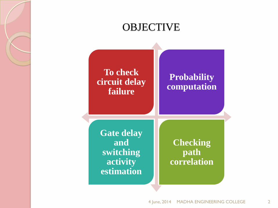
OBJECTIVE
4 June, 2014 MADHA ENGINEERING COLLEGE
To check circuit delay
failure
Probability computation
Gate delay and
switching activity
estimation
Checking path
correlation
2
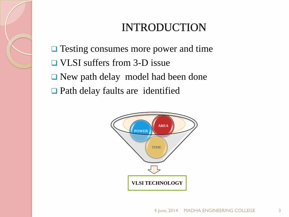
INTRODUCTION
Testing consumes more power and time
VLSI suffers from 3-D issue
New path delay model had been done
Path delay faults are identified
4 June, 2014 MADHA ENGINEERING COLLEGE
VLSI TECHNOLOGY
TIME
POWER
AREA
3
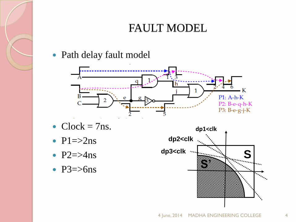
FAULT MODEL
4 June, 2014 MADHA ENGINEERING COLLEGE
Path delay fault model
Clock = 7ns.
P1=>2ns
P2=>4ns
P3=>6ns
SS’
dp2<clk
dp3<clk
dp1<clk
4
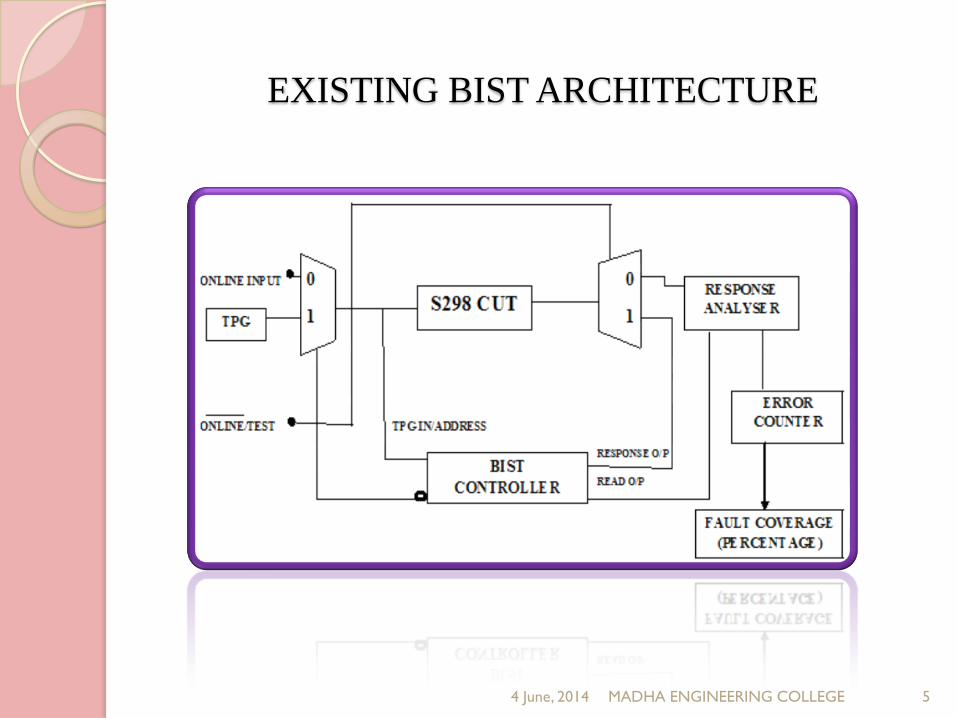
EXISTING BIST ARCHITECTURE
4 June, 2014 MADHA ENGINEERING COLLEGE 5
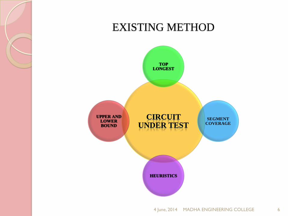
EXISTING METHOD
4 June, 2014 MADHA ENGINEERING COLLEGE
CIRCUIT UNDER TEST
TOP LONGEST
SEGMENT COVERAGE
HEURISTICS
UPPER AND LOWER BOUND
6
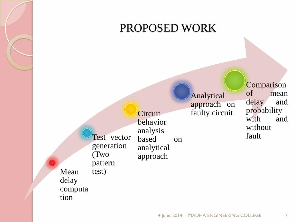
PROPOSED WORK
Meandelaycomputation
Test vectorgeneration(Twopatterntest)
Circuitbehavioranalysisbased onanalyticalapproach
Analyticalapproach onfaulty circuit
Comparisonof meandelay andprobabilitywith andwithoutfault
4 June, 2014 MADHA ENGINEERING COLLEGE 7
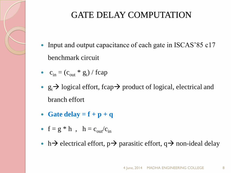
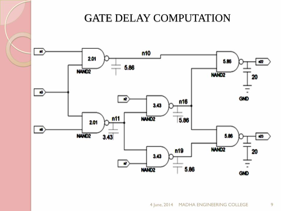
GATE DELAY COMPUTATION
4 June, 2014 MADHA ENGINEERING COLLEGE
Input and output capacitance of each gate in ISCAS’85 c17
benchmark circuit
cin = (cout * gi) / fcap
gi logical effort, fcap product of logical, electrical and
branch effort
Gate delay = f + p + q
f = g * h , h = cout/cin
h electrical effort, p parasitic effort, q non-ideal delay
8
GATE DELAY COMPUTATION
4 June, 2014 MADHA ENGINEERING COLLEGE 9
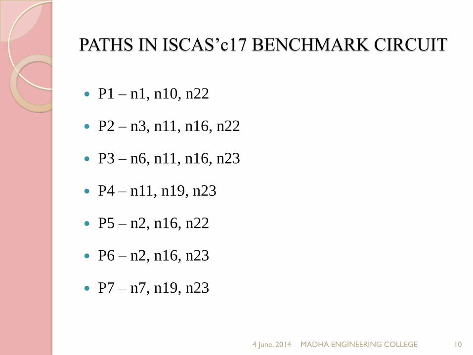
PATHS IN ISCAS’c17 BENCHMARK CIRCUIT
P1 – n1, n10, n22
P2 – n3, n11, n16, n22
P3 – n6, n11, n16, n23
P4 – n11, n19, n23
P5 – n2, n16, n22
P6 – n2, n16, n23
P7 – n7, n19, n23
4 June, 2014 MADHA ENGINEERING COLLEGE 10
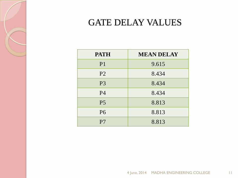
GATE DELAY VALUES
4 June, 2014 MADHA ENGINEERING COLLEGE
PATH MEAN DELAY
P1 9.615
P2 8.434
P3 8.434
P4 8.434
P5 8.813
P6 8.813
P7 8.813
11
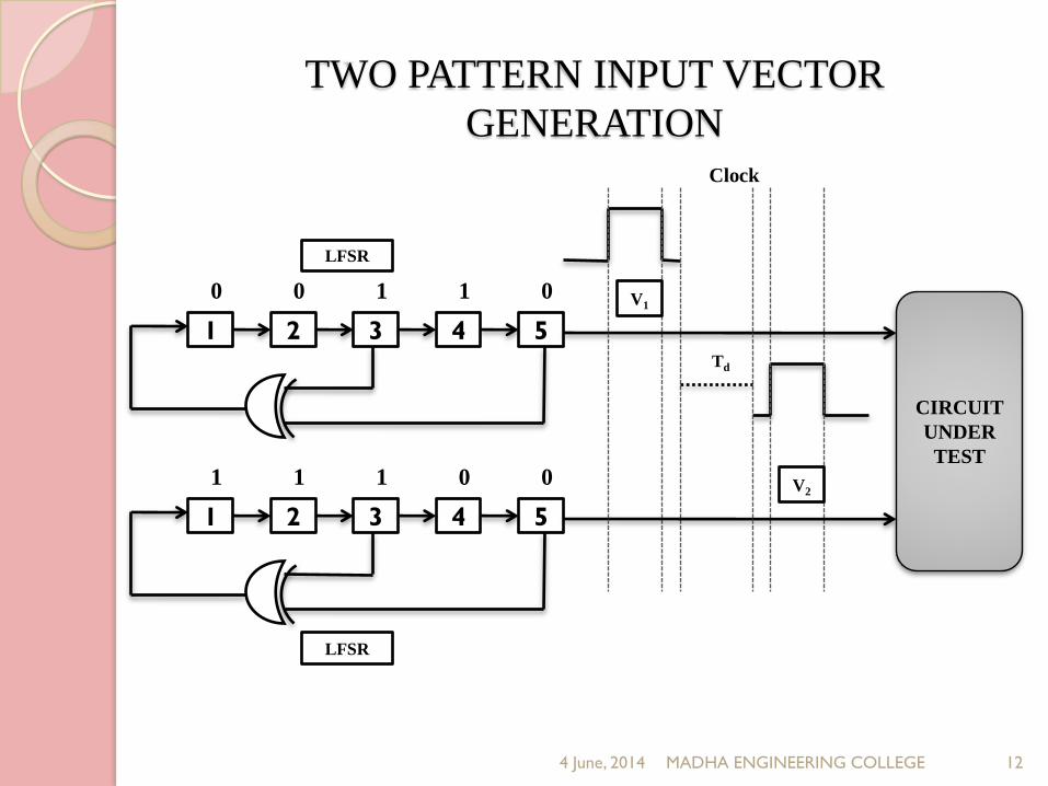
TWO PATTERN INPUT VECTOR
GENERATION
4 June, 2014 MADHA ENGINEERING COLLEGE
1 2 3 4 5
0 0 1 1 0
1 2 3 4 5
1 1 1 0 0
CIRCUIT
UNDER
TEST
LFSR
LFSR
Clock
V1
V2
Td
12
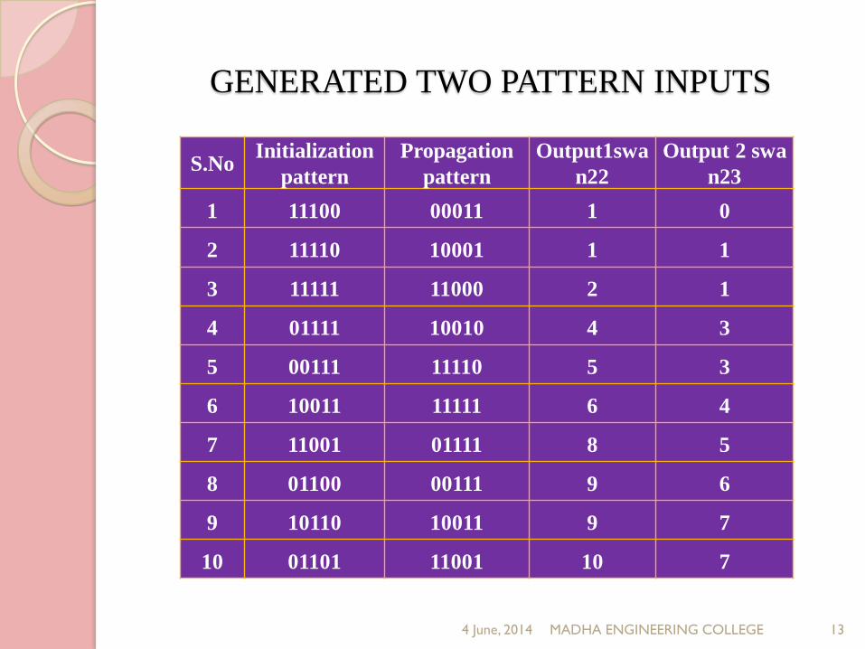
GENERATED TWO PATTERN INPUTS
4 June, 2014 MADHA ENGINEERING COLLEGE
S.NoInitialization
pattern
Propagation
pattern
Output1swa
n22
Output 2 swa
n23
1 11100 00011 1 0
2 11110 10001 1 1
3 11111 11000 2 1
4 01111 10010 4 3
5 00111 11110 5 3
6 10011 11111 6 4
7 11001 01111 8 5
8 01100 00111 9 6
9 10110 10011 9 7
10 01101 11001 10 7
13
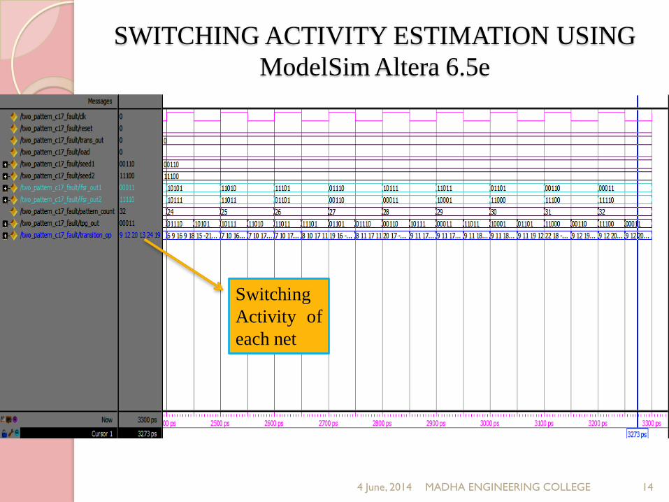
SWITCHING ACTIVITY ESTIMATION USING
ModelSim Altera 6.5e
4 June, 2014 MADHA ENGINEERING COLLEGE
Switching
Activity of
each net
14
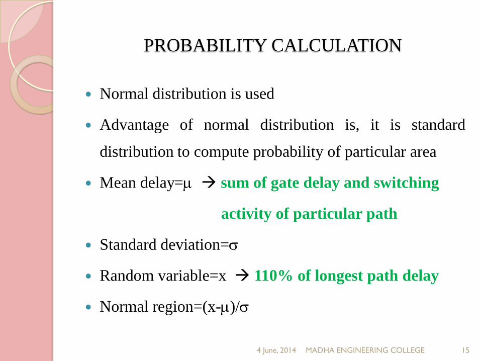
PROBABILITY CALCULATION
Normal distribution is used
Advantage of normal distribution is, it is standard
distribution to compute probability of particular area
Mean delay=m sum of gate delay and switching
activity of particular path
Standard deviation=s
Random variable=x 110% of longest path delay
Normal region=(x-m)/s
4 June, 2014 MADHA ENGINEERING COLLEGE 15
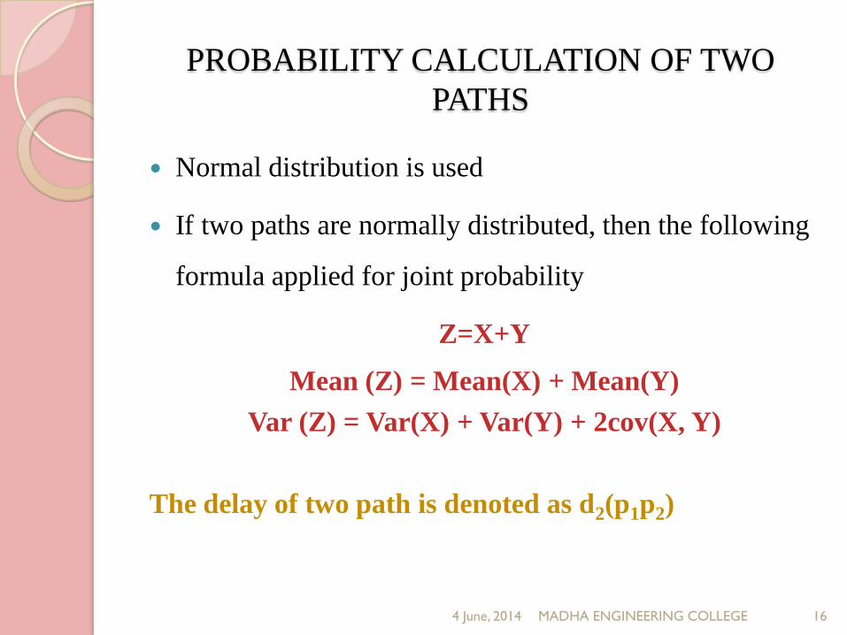
PROBABILITY CALCULATION OF TWO
PATHS
Normal distribution is used
If two paths are normally distributed, then the following
formula applied for joint probability
Z=X+Y
Mean (Z) = Mean(X) + Mean(Y)
Var (Z) = Var(X) + Var(Y) + 2cov(X, Y)
The delay of two path is denoted as d2(p1p2)
4 June, 2014 MADHA ENGINEERING COLLEGE 16
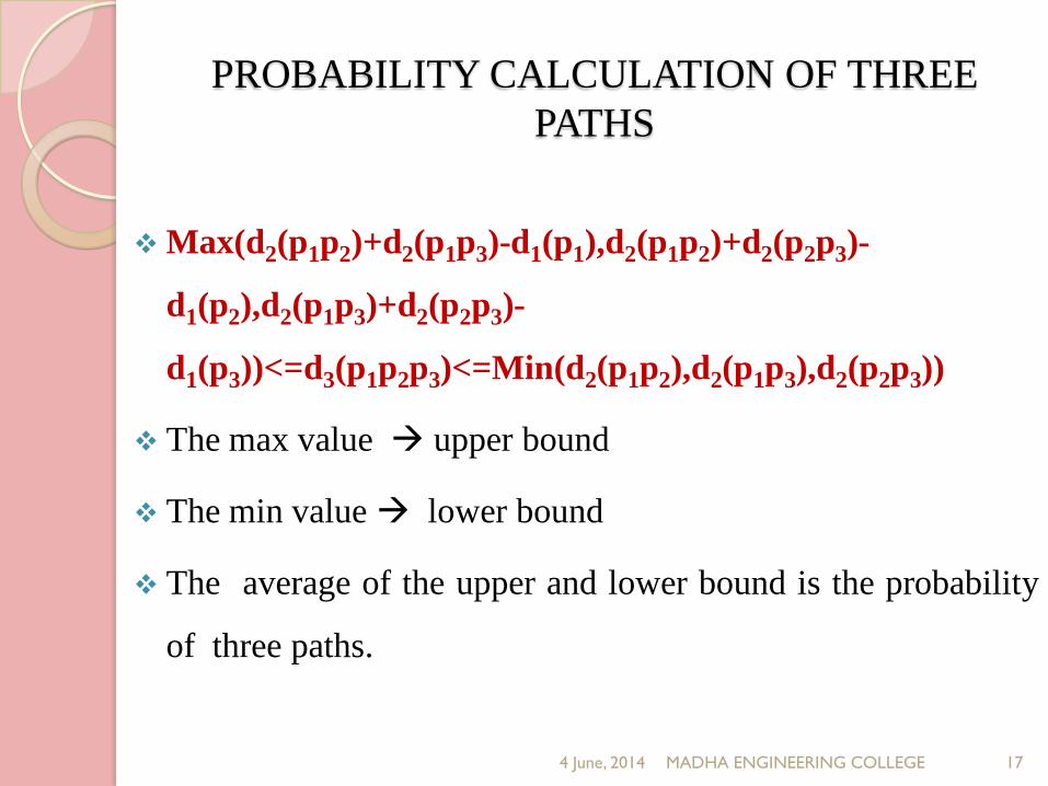
PROBABILITY CALCULATION OF THREE
PATHS
Max(d2(p1p2)+d2(p1p3)-d1(p1),d2(p1p2)+d2(p2p3)-
d1(p2),d2(p1p3)+d2(p2p3)-
d1(p3))<=d3(p1p2p3)<=Min(d2(p1p2),d2(p1p3),d2(p2p3))
The max value upper bound
The min value lower bound
The average of the upper and lower bound is the probability
of three paths.
4 June, 2014 MADHA ENGINEERING COLLEGE 17
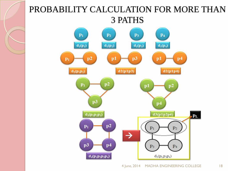
PROBABILITY CALCULATION FOR MORE THAN
3 PATHS
4 June, 2014 MADHA ENGINEERING COLLEGE 18
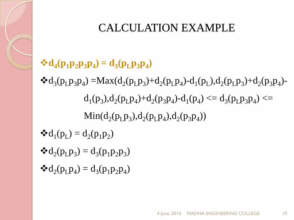
CALCULATION EXAMPLE
4 June, 2014 MADHA ENGINEERING COLLEGE
d4(p1p2p3p4) = d3(pLp3p4)
d3(pLp3p4) =Max(d2(pLp3)+d2(pLp4)-d1(pL),d2(pLp3)+d2(p3p4)-
d1(p3),d2(pLp4)+d2(p3p4)-d1(p4) <= d3(pLp3p4) <=
Min(d2(pLp3),d2(pLp4),d2(p3p4))
d1(pL) = d2(p1p2)
d2(pLp3) = d3(p1p2p3)
d2(pLp4) = d3(p1p2p4)
19
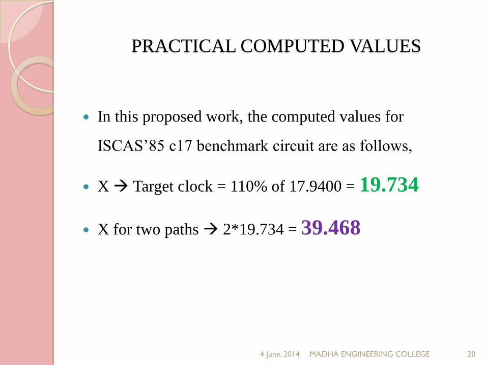
PRACTICAL COMPUTED VALUES
In this proposed work, the computed values for
ISCAS’85 c17 benchmark circuit are as follows,
X Target clock = 110% of 17.9400 = 19.734
X for two paths 2*19.734 = 39.468
4 June, 2014 MADHA ENGINEERING COLLEGE 20
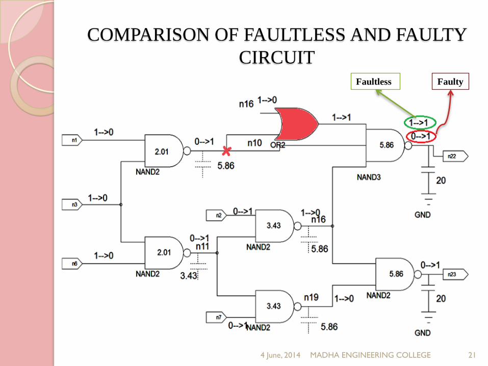
COMPARISON OF FAULTLESS AND FAULTY
CIRCUIT
4 June, 2014 MADHA ENGINEERING COLLEGE
Faultless Faulty
21
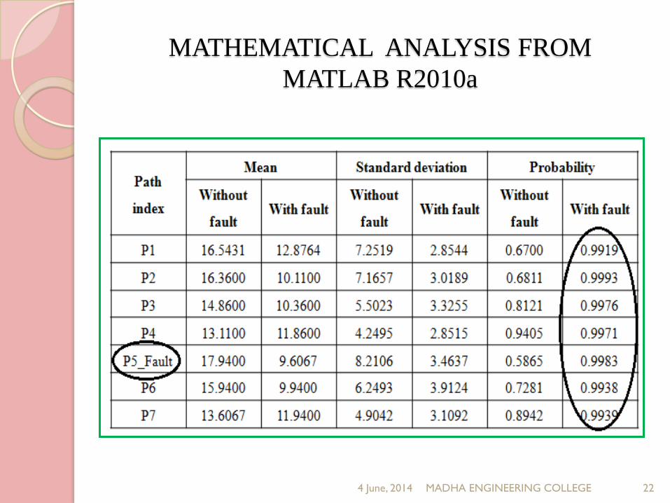
MATHEMATICAL ANALYSIS FROM
MATLAB R2010a
4 June, 2014 MADHA ENGINEERING COLLEGE 22
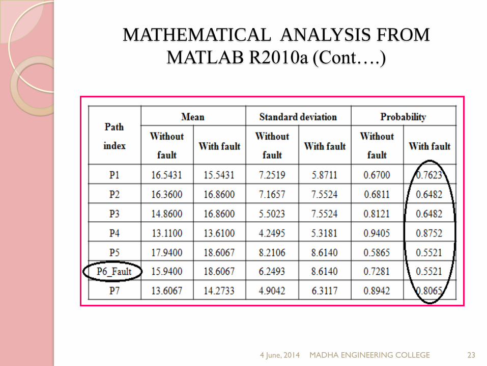
MATHEMATICAL ANALYSIS FROM
MATLAB R2010a (Cont….)
4 June, 2014 MADHA ENGINEERING COLLEGE 23
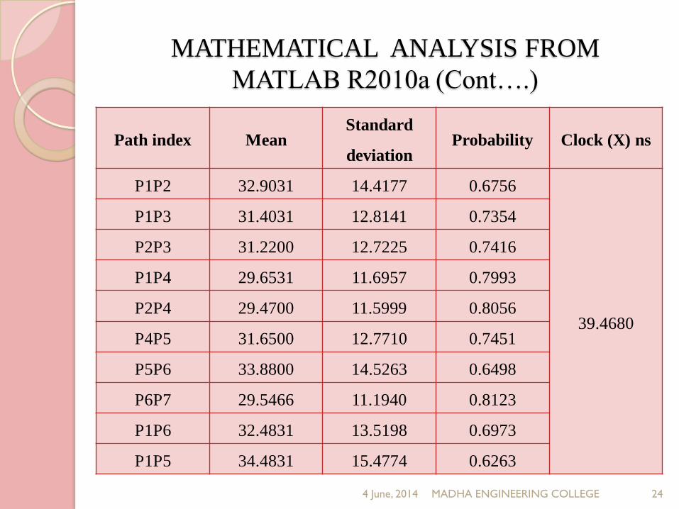
MATHEMATICAL ANALYSIS FROM
MATLAB R2010a (Cont….)
4 June, 2014 MADHA ENGINEERING COLLEGE
Path index MeanStandard
deviationProbability Clock (X) ns
P1P2 32.9031 14.4177 0.6756
39.4680
P1P3 31.4031 12.8141 0.7354
P2P3 31.2200 12.7225 0.7416
P1P4 29.6531 11.6957 0.7993
P2P4 29.4700 11.5999 0.8056
P4P5 31.6500 12.7710 0.7451
P5P6 33.8800 14.5263 0.6498
P6P7 29.5466 11.1940 0.8123
P1P6 32.4831 13.5198 0.6973
P1P5 34.4831 15.4774 0.6263
24
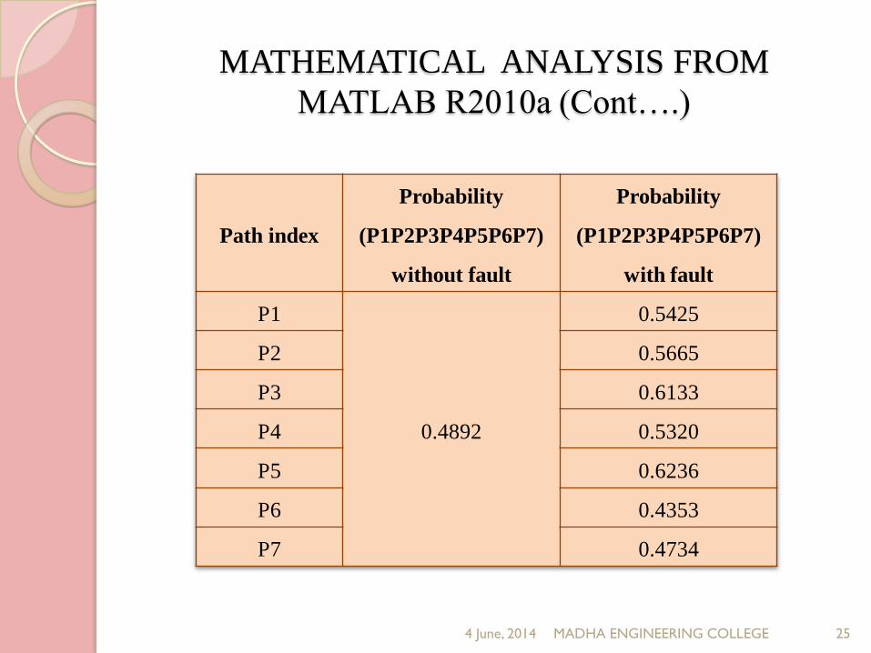
MATHEMATICAL ANALYSIS FROM
MATLAB R2010a (Cont….)
4 June, 2014 MADHA ENGINEERING COLLEGE
Path index
Probability
(P1P2P3P4P5P6P7)
without fault
Probability
(P1P2P3P4P5P6P7)
with fault
P1
0.4892
0.5425
P2 0.5665
P3 0.6133
P4 0.5320
P5 0.6236
P6 0.4353
P7 0.4734
25
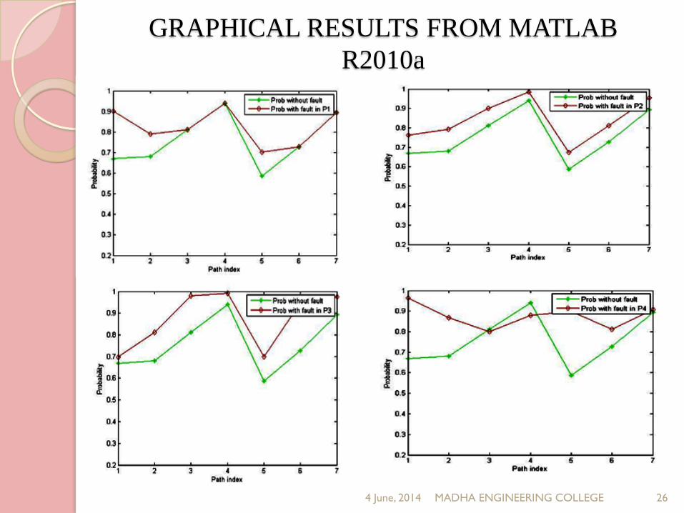
GRAPHICAL RESULTS FROM MATLAB
R2010a
4 June, 2014 MADHA ENGINEERING COLLEGE 26
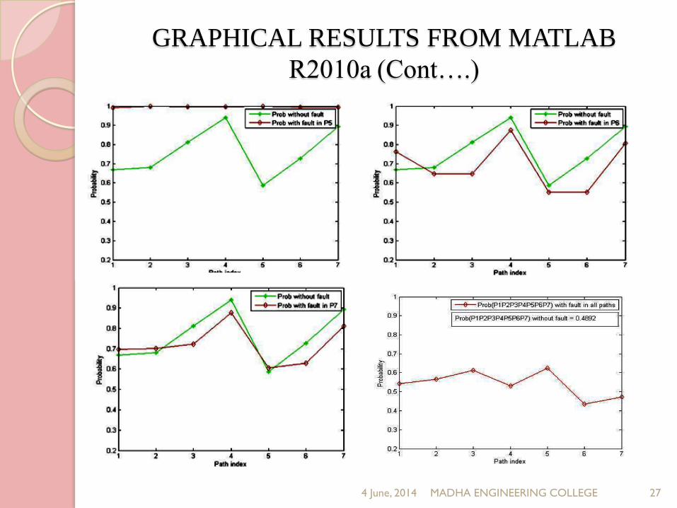
GRAPHICAL RESULTS FROM MATLAB
R2010a (Cont….)
4 June, 2014 MADHA ENGINEERING COLLEGE 27
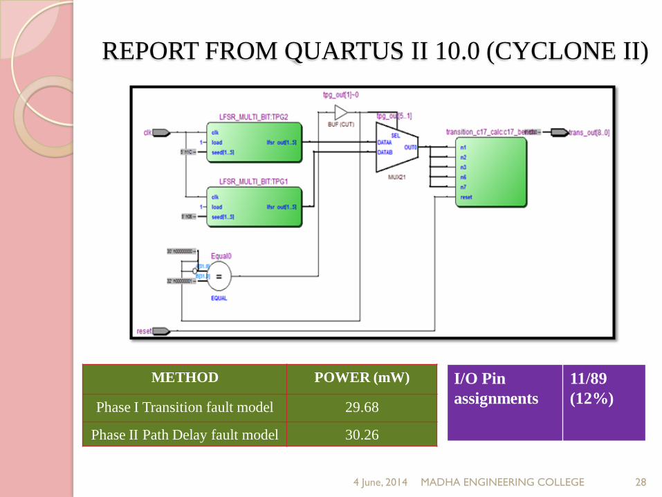
REPORT FROM QUARTUS II 10.0 (CYCLONE II)
METHOD POWER (mW)
Phase I Transition fault model 29.68
Phase II Path Delay fault model 30.26
4 June, 2014 MADHA ENGINEERING COLLEGE
I/O Pin
assignments
11/89
(12%)
28
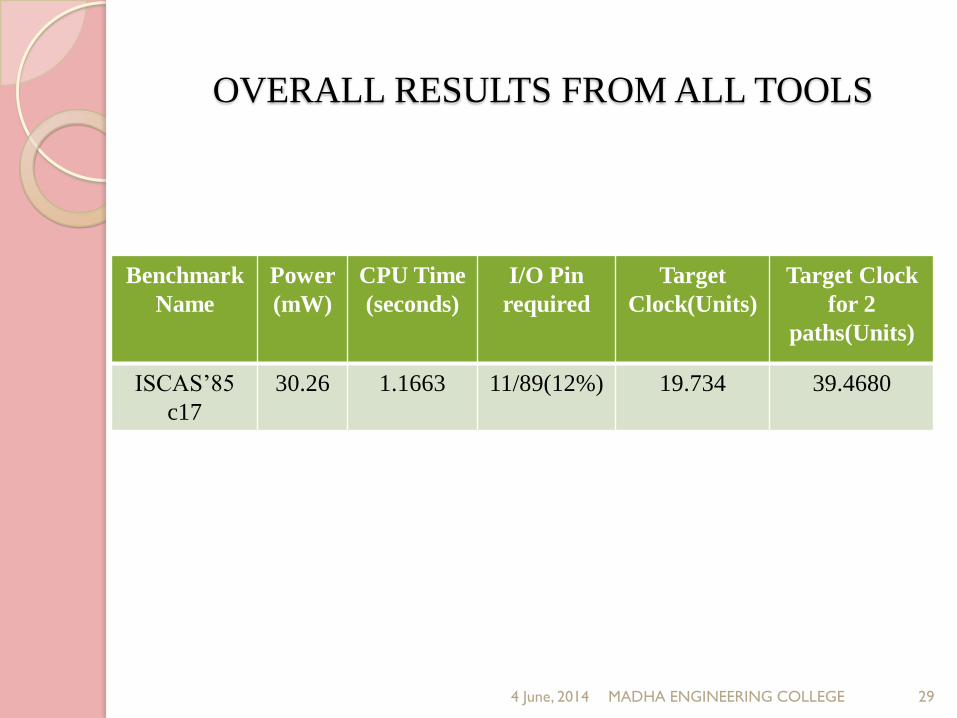
OVERALL RESULTS FROM ALL TOOLS
Benchmark
Name
Power
(mW)
CPU Time
(seconds)
I/O Pin
required
Target
Clock(Units)
Target Clock
for 2
paths(Units)
ISCAS’85
c17
30.26 1.1663 11/89(12%) 19.734 39.4680
4 June, 2014 MADHA ENGINEERING COLLEGE 29
CONCLUSION
The probability value depends on the switching activity
of the circuit
The circuit switching activity in turn depends on the
input vectors.
If the probability is high, the path delay will not exceed
the maximum delay
If the probability is low, the path delay will exceed the
maximum delay.
4 June, 2014 MADHA ENGINEERING COLLEGE 30
FUTURE WORK
4 June, 2014 MADHA ENGINEERING COLLEGE
In future work, interconnect delay also considered with
gate delay, switching activity of the nets with primary
input vectors so as to achieve accurate path delay for
small and large circuits.
31
REFERENCES
[1] Alok S. Doshi and Anand S(2008), “Test Pattern Generator for Built-in Self Test using Spectral Methods ” , Mudlapur
Auburn University Dept. of Electrical and Computer Engineering, Auburn, AL, USA doshias.
[2] Hongliang Chang and Sachin S. Sapatnekar(2003), “Statistical Timing Analysis Under Spatial Correlations,” Fellow,
IEEE.”Computer Aided Design of integrated circuits and systems, IEEE Transactions on vol 24, no. 9.
[3] lrith Pomeranz and Sudhakar M. Reddy(Jan.1996), “On the number of tests to delect all path delay faults in combinational
logic circuits, “IEEE transactions on computers, vol. 45, No. 1.
[4] Jing-Jia Liou, Angela Krstic, Li-C. Wang and Kwang-Ting Cheng(Jun 2002), “False-Path-Aware Statistical Timing
Analysis and Efficient Path Selection for Delay Testing and Timing Validation,” Electrical and Computer Engineering
Department,University of California, Santa Barbara., IEEE 39th proceedings.
[5] Li-C. Wang, Jing-Jia Liou and Kwang-Ting Cheng(Nov 2004), “Critical Path Selection for Delay Fault Testing Based
Upon a Statistical Timing Model,” IEEE transactions on computer-aided design of integrated circuits and systems, vol. 23,
no. 11,.
[6] Vladimir Zolotov, Jinjun Xiong, Hanif Fatemi,and Chandu Visweswariah(May 2010), “Statistical Path Selection for At-
Speed Test,” IEEE transactions on computer-aided design of integrated circuits and systems, vol. 29, no. 5.
[7] W.B.Jone, W.S.Yeh and S.R.Das(2000),”An Adaptive Path Selection Method for Delay Testing”, IEEE transactions on
very large scale integration system, volume 50, issue 5.
[8] Wing Ning Li, Sudhakar M. Reddy, Sartaj Sahni(Aug 2002), “On Path Selection In Combinational Logic Circuits,” IEEE
transactions in computer aided design of integrated circuits and systems, vol 8, no. 1.
[9] Wangqi Qiu D. M. H. Walker, “An Efficient Algorithm for Finding the K Longest Testable Paths Through Each Gate in a
Combinational Circuit,” Department of Computer ScienceTexas A&M University, IEEE proceedings, volume 1.
[10] Xiang Lu, Zhuo Li, Wangqi Qiu, D. M. H. Walker and Weiping Shi, “Longest Path Selection for Delay Test under Process
Variation,” Texas A&M University, College Station, Texas 77843, IEEE transactions on vol 24, no. 12.
[11] Zijian He, Tao Lv, Huawei Li and Xiaowei Li(Jul 2013), “Test Path Selection for Capturing Delay Failures Under
Statistical Timing Model”IEEE transactions on very large scale integration (VLSI) systems, vol. 21, No. 7.
4 June, 2014 MADHA ENGINEERING COLLEGE 32

4 June, 2014 MADHA ENGINEERING COLLEGE 33