a new mosfet model for the simulation of circuits under ... · a new mosfet model for the...
TRANSCRIPT

A New MOSFET Model for the Simulation
of Circuits under Mechanical Stress
Heidrun Alius*, Horst Rempp**, Zili Yu** and Thomas Gneiting*
*AdMOS GmbH (Germany), **IMS-CHIPS (Germany)
MOS-AK Workshop, London, March 2014

• Introduction Thin Microsystem
• Background - Piezo electrical effect
• Modeling approach
Verilog-A Implementation
Enhancing a standard MOS model for special effects
Equations
• Experiments
measurements on bended devices
parameter extractions
• Verification with circuits on bended chips
• Summary
2
Content
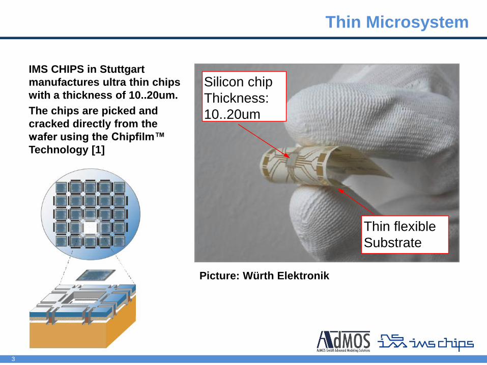
IMS CHIPS in Stuttgart
manufactures ultra thin chips
with a thickness of 10..20um.
The chips are picked and
cracked directly from the
wafer using the Chipfilm™
Technology [1]
3
Thin Microsystem
Silicon chip
Thickness:
10..20um
Thin flexible
Substrate
Picture: Würth Elektronik

Thin chips are embedded in flexible substrates
like Polyimide or LCP [2].
The total thickness of the microsystem is 100 …
150um.
4
Thin Microsystem
Silicon chip
Metal on Si chip
Microvia in upper Cu
layer
Lower Cu layer
LCP substrate

5
Possible applications
The picture shows a possible
application as an intelligent
plaster
• An ultrathin chip is
embedded in a flexible foil.
• It can be applied e.g. on a
human knee to monitor the
bending of the knee and
other body parameters.

6
Thin Microsystem
The research work is carried out in a joint project
„PRONTO – Ultimum“ which is part of the leading-edge research
cluster .
Project partners are:
• IMS Chips, Stuttgart
• Robert Bosch, Stuttgart
• Würth Elektronik, Rot am See
• AdMOS, Frickenhausen
The project is funded by the German Federal
Ministry of Education and Research,
project no. 16SV5135.

• The mechanical stress applied on a MOSFET leads to the change of carrier
mobilitiy (µ0).
• Due to the direct proportionality of drain current and carrier mobility (µ0), the drain
current would also change under mechanical stress (Fig. 1).
• The sensitivity of drain current to stress depends on the layout orientation of
MOSFET channels and the direction of the applied stress (Fig. 2).
7
Piezoresistive Effect in MOSFET
Fig. 1 Drain current vs. uniaxial stress for
PMOS transistors
Fig. 2 Illustration of MOSFET channel layout
orientation (represented by angle θ) respect to stress
direction (represented by angle φ)

8
Modeling Approach – Verilog-A Implementation
PSP 103.1
Compact Model Council
Standard MOS Model
Already integrated in many
commercial and public domain
simulators
Verilog-A Code
+ Extensions for:
- Selfheating
- Stress
- ……
PSP 103_Ultimum
Para-
meter
Library with standard PSP
103 model parameters for
IMS 0.5um CMOS
Extension for thin chip
specific paramters Stress,
..
+
[3]

9
Integration of Stress in the PSP Model
→ Low field mobility
→ High field mobility
→ Threshold voltage
Original PSP
parameter
without stress
Contribution of
the bending
(curvature)
Contribution of the
stress orientation
versus the crystal
orientation of the
wafer
New effective
model
parameter
including stress
Based on the theoretical description of the piezo electrical effect and the
observed behaviour of the tested transistors, the following parameters in the PSP
model are modified:

New instance parameters:
CURVation = 1/R = -2.61m – 2.61m
ORIENTation = 0°, 45°, 90°
10
Integration of Stress in the PSP Model
New model parameters:
h = 675 µm thickness of wafer
E = 160 GPa, Young‘s Modulus of Si
STUO, STUOL, STUOW, STUOLW
STSATO, STSATL, STSATW, STSATLW
STVTHO, STVTHL, STVTHW, STVTHLW
ORIUO, ORISAT, ORIVTH
Stress vs. Crystal orientation
Stress Magnitude
Magnitude of
mechanical
Tension
Dimension
dependency

11
Integration of Selfheating in the PSP Model
New electrical Node T
Transistor temperature:
TKD = $temperature + DTA
RTH_i = RTHO + RTHW * W / NFRTHNF
Ptotal = UDS * IDS I(T) <+ V(T) / RTH_i
∆T = Ptotal * RTH_i I(T) <+ - abs(Ids * Vds)
New model parameters:
RTHO, RTHW, RTHNF (global)
RTH (local)
+ V(T)

• Introduction Thin Microsystem
• Background - Piezo electrical effect
• Modeling approach
Verilog-A Implementation:
Enhancing a standard MOS model for special effects (HA)
Equations
• Experiments
measurements on bended thick devices
parameter extractions
• Verification with circuits on bended chips
• Summary
12
Content

13
Test Devices for Model Parameter Extraction
• IMS-CHIPS 0.5 µm CMOS technology.
• Test chip consists of various MOSFET modules (Fig. 3).
• Test chip is on a wafer stripe and is wire-bonded to a flex circuit (Fig. 4).
• A four-point bending system is used to apply defined mechanical stress to the chip
under test (Fig. 5).
Fig. 3 IMS-CHIPS 0.5 µm test chip layout: (a)Test chip with various test
modules. (b) A test module with various MOSFETs. (c) A MOSFET pair with
orthogonal layout orientations.
(a) (b) (c)
Fig. 4 The test chip is on a wafer stripe and is wire-bonded to a flex circuit.
(a)
(b)
Fig. 5 Four-point
bending system:
(a) Illustration of
the system. (b)
Photo of the test
system.
14
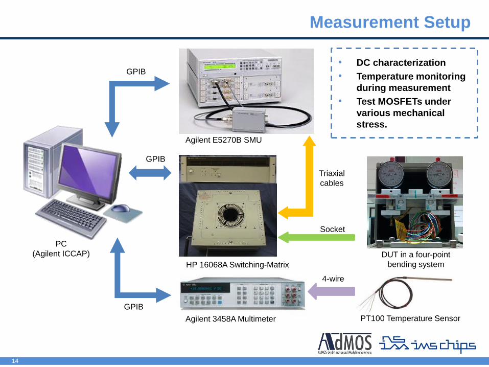
Measurement Setup
PC
(Agilent ICCAP)
Agilent E5270B SMU
HP 16068A Switching-Matrix
Agilent 3458A Multimeter PT100 Temperature Sensor
DUT in a four-point
bending system
GPIB
GPIB
GPIB
Triaxial
cables
Socket
4-wire
• DC characterization
• Temperature monitoring
during measurement
• Test MOSFETs under
various mechanical
stress.

• Sweep Vd, Vg and Vb.
• Outputs: Id, Ib
• Temperature is captured during the measurement.
• MOSFETs with various W/L ratios are measured.
15
Measurement Dataset
y = 5.1212E-04x + 2.4601E-17
y = 2.93E-04x + 1.29E-16
y = -4.2457E-04x + 1.2300E-17
y = -3.0497E-04x + 1.1685E-16
-0,06
-0,04
-0,02
0
0,02
0,04
0,06
0,08
0 20 40 60 80 100 120 140 160
(id
s-id
s0)/
ids0
×1
00
%
stress (MPa)n (100mV) n (5) rot (100mV) rot (5)
PMOSW/L =10 µm/ 0.55 µm Vb=0 Vds=100mV or 5V Vgs= 5Vnormal (=longitudinal)rot (=transversal)
-> πlong = 293*10-12 1/Pa
-> πtrans = - 305*10-12 1/Pa
-> πlong = 512*10-12 1/Pa
-> πtrans = - 425*10-12 1/Pa
Compresive stress
0,0E+00
2,0E-06
4,0E-06
6,0E-06
8,0E-06
1,0E-05
1,2E-05
0 1 2 3 4 5
Ids
(A)
Vgs (V)
100 mV 5 V
PMOSW/L =0.7 µm / 10 µmvb=0 vds=100mV or 5V vgs= 5V
Flat conditioninput characteristics
Fig. 6 Input characteristic of a PMOS Fig. 7 Current variation under compresive stress
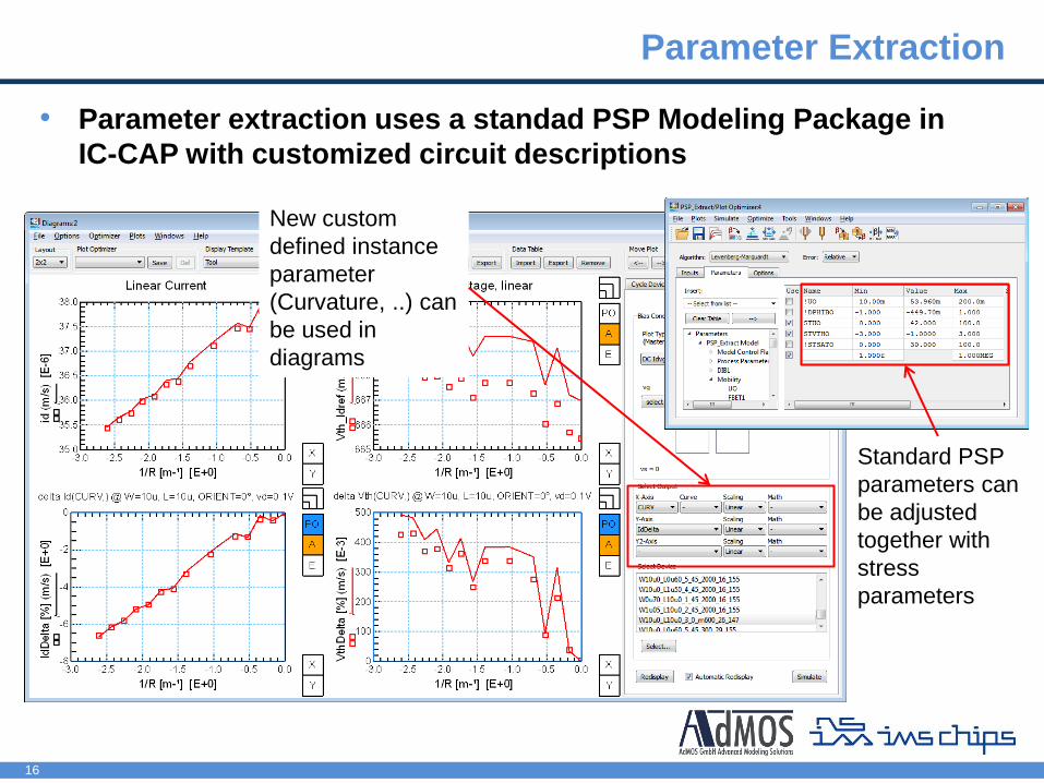
• Parameter extraction uses a standad PSP Modeling Package in
IC-CAP with customized circuit descriptions
16
Parameter Extraction
Standard PSP
parameters can
be adjusted
together with
stress
parameters
New custom
defined instance
parameter
(Curvature, ..) can
be used in
diagrams

17
Simulation Model Including Stress
Transfer characteristic, logarithmical Transfer characteristic
Output characteristic
measured
— simulated
CURV
— 0
— -2.61 Compression

18
Simulation Model including Stress
Saturation current Threshold voltage
measured
— simulated
• Output Id of a NMOS transistor is shown
• Measured data has a temperature variation for different bending conditions
DTA (around 1K).
• The temperature is recorded for each case and is taken into account for the
simulation. This results in the ragged curves !
• Instance parameters:
Width = 10 µm, Length = 10 µm, Curvation = 1/R = CURV = 0…-2.61 m-1, DTA

19
Transisor in Compression + Tension
• Output Id of a short PMOS Transistor, measured at two different modules
• Instance parameters:
Width = 10 µm, Length = 10 µm, CURV (1/R) = ±2.61/m, ORIENT = 0°
MODUL
— 148
— 149
∆Id(CURV) linear current ∆Id(CURV) saturation current
∆Vth(CURV) linear region ∆Vth(CURV, ORIENT) saturation region
Tension Compression
measured
— simulated

20
Length Dependency of Stress
NMOS linear current ∆Id(L, ORIENT) NMOS saturation current ∆Id(L, ORIENT)
• Instance parameters:
Width = 10 µm, CURV (1/R) = ±2.61 m-1, ORIENT = 0°, 45°, 90°
ORIENT / CURV
— 0° / -2.61 m-1 Compres.
— 45° / 2.61 m-1
— 90° / -2.61 m-1 Compres.
measured
— simulated NMOS
PMOS
ORIENT / CURV
— 0° / 2.61 m-1
— 45° / 2.61 m-1
— 90° / 2.61 m-1

21
Dependency of Stress over Orientation
NMOS linear current ∆Id( ORIENT, CURV) ∆Id(ORIENT, CURV) saturation region
measured
— simulated
• Instance parameters:
Width = 10 µm, Length = 10 µm, CURV (1/R) = ± 2.61/m
• Model parameters:
ORIPHI=1.0, ORIUO=0.18, ORISAT=0.0, ORIVTH=0.33, E=160 GPa, h=675 µm
CURV
— 2.61 Tension
— -2.61 Compression
NMOS
PMOS

22
Verification with CMOS Circuit (1)
Fig. 8 Test Circuits: (a) NMOS current mirror with resistive load, (b) PMOS
current mirror with resistive load.(Resistors are off-chip components)
y = -1,27E-04x - 3,76E-03
y = -1.25E-04x + 4.78E-02
-3,0000E-01
-2,0000E-01
-1,0000E-01
0,0000E+00
1,0000E-01
2,0000E-01
3,0000E-01
-2000 -1500 -1000 -500 0 500 1000 1500 2000 2500
Vd
iff(V
)
Deflection (µm)
Vdiff_simu
Vsiff_mea
Linear (Vdiff_simu)
Linear (Vsiff_mea)
PMOS pairM1: 0°M2: 90°W/L=8.8µm/1.55µmMult=2
• Test circuit: Current
mirror with resistive
load, four different
MOSFET combinations.
• Simulation using the
PSP model.
• Compare the simulation
results with
measurement results.
y = 1,93E-10x + 1,10E-04
y = 2,20947E-10x + 0,000111621
1,0950E-04
1,1000E-04
1,1050E-04
1,1100E-04
1,1150E-04
1,1200E-04
1,1250E-04
-2000 -1500 -1000 -500 0 500 1000 1500 2000 2500
I d2
(A)
Deflection (µm)
Id2_simu
Id2_mea
Linear (Id2_simu)
Linear (Id2_mea)
NMOS pairM1: 45°M2: 135°W/L=8.8µm/1.55µmMult=2
Fig. 9 NMOS current mirror (45°/135°) with resistive load,
Vdiff/deflection. Fig. 10 PMOS current mirror (0°/90°) with resistive load,
Vdiff/deflection

23
Verification with CMOS Circuit (2)
Summary Slopes Comments
MOS Type M1 M2 Vdiff_simu Vdiff_measure
NMOS 45° 135° 0 1.24E-06 Measured current mirror pair shows very low
sensitivity to bending, which is approaching the theoretical value 0.
NMOS 0° 90° -2.22E-05 -2.08E-05 Measurement and simulation show good agreement.
PMOS 0° 90° -1.27E-04 -1.25E-04 Measurement and simulation show good agreement.
PMOS 45° 135° 0 -4.03E-06 Measured current mirror pair shows very low
sensitivity to bending, which is approaching the theoretical value 0.
Results Summary:
• DC offset has been observed during measurement, which is due to device
mismatch.
• Both simulation and measurement show similar stress sensitivity. Good
agreement has been achieved.

• The paper gave an introduction to highly flexible ultrathin
microsystems incorporating very thin silicon chips.
• The bending of the chips causes a change in the electrical
behavior of the MOS transistors due to the piezo electrical effect.
• This effect was integrated into a standard MOS model (PSP 103.1).
• The changes were done in Verilog-A and the model PSP_Ultimum
was implemented into the design environments of the project
partners.
• The feasibility of this approach could be demonstrated in an
application, where current mirrors were used to detect bending.
Simulations and measurements of the circuits showed an excellent
agreement.
24
Summary

(1) “MOST Modeling for Ultra-thin Flexible Electronics”, J. Burghartz,
N. Wacker, M. Hassan, H. Rempp, H. Richter, MOS-AK 2009,
Athens
(2) "Flexible Schaltungsträger mit eingebetteten, flexiblen ICs“,
Jürgen Wolf, Christine Harendt, Jan Kostelnik, Andreas Kugler,
Horst Rempp, ELB - Elektronische Baugruppen und Leiterplatten
Fachtagung, Fellbach
(3) "Design und Simulation: Thermomechanischer Stress,
elektrisches Verhalten beim Leiterplatten-Embedding“, Thomas
Gneiting. 3. GMM Workshop - Packaging von Mikrosystemen
PackMEMS 2012, Stuttgart
25
Literature